rights / license: research collection in copyright - non ...41940/...acknowledgements over the last...
TRANSCRIPT

Research Collection
Doctoral Thesis
A TCAD analysis of long-wavelength vertical-cavity surface-emitting lasers
Author(s): Bäcker, Alexandra
Publication Date: 2009
Permanent Link: https://doi.org/10.3929/ethz-a-005842398
Rights / License: In Copyright - Non-Commercial Use Permitted
This page was generated automatically upon download from the ETH Zurich Research Collection. For moreinformation please consult the Terms of use.
ETH Library

A TCAD Analysis of Long-Wavelength Vertical-
Cavity Surface-Emitting Lasers


Diss. ETH No. 18330
A TCAD Analysis of
Long-Wavelength
Vertical-Cavity
Surface-Emitting Lasers
A dissertation submitted to the
SWISS FEDERAL INSTITUTE OF TECHNOLOGY
ZURICH
for the degree of
DOCTOR OF SCIENCES
presented by
ALEXANDRA BACKER
Dipl.-Ing., TU Wien
born January 20, 1980
citizen of Austria
accepted on the recommendation of
Prof. Dr. Bernd Witzigmann, examiner
Prof. Dr. Heinz Jackel, co-examiner
2009


Acknowledgements
Over the last four years I had the pleasure to work in the Computa-tional Optoelectronics (COE) Group at the Integrated Systems Lab-oratory (IIS) at ETH Zurich. First of all, I wish to thank Prof. BerndWitzigmann for giving me the opportunity to perform this work un-der his supervision. I would also like to thank Prof. Heinz Jackel fromthe Electronics Laboratory at ETH Zurich for accepting to be theco-examiner of this thesis.
I wish to thank Prof. Eli Kapon at EPF Lausanne for inviting meto spend 6 months in 2007 with his Laboratory of Nanostructures asa visiting scientist. I am very grateful to Christine Haller at ETHZurich and Denise Paroz at EPF Lausanne for their great support inorganizational matters concerning my stay at EPF Lausanne.
Work would not have been the same without the current and for-mer members of the COE group at IIS. A big thank you goes to allof you for many interesting discussions and the fun: Hektor Meier,Philipp Kreuter, Dr. Sebastian Seiger, Dr. Ratko Veprek, Dr. Mar-tin Loeser, Denis Dolgos, Jan Kupec, Dr. Stefan Odermatt, SlimMakhlouka, Dr. Matthias Streiff, Dr. Valerio Laino, Dr. FriedhardRomer, Dr. Lutz Schneider and Dr. Biju Jacobs. I would also like tomention my non-COE office mates over the years. You were greattoo: Dr. Mathieu Luisier, Christian Benkeser, Dr. Stefan Holzer,Dr. Alexander Koschik and Dr. Norio Sato. Special thanks go toDr. Chiara Martelli for the organization of many ”IIS“-evenings inthe cinema and weekends of snowboarding.
The work for this thesis was conducted in close collaboration withindustry. I want to thank the entire team of BeamExpress SA, espe-cially Dr. Paul Royo and Dr. Vladimir Iakovlev, for providing me with
v

vi ACKNOWLEDGEMENTS
device and measurement data as well as for many interesting discus-sions in Lausanne. Tackling the simulational hurdles would not havebeen possible without the input from Synopsys Switzerland LLC, es-pecially Dr. Stefan Odermatt, Dr. Gergo Letay, Rafael Santschi and,formerly, Adrian Bregy.
The technical and administrative staff at the IIS did a great jobin providing excellent working conditions. First of all, I would like tothank the computer administration, Christoph Wicki, Adam Feiginand, formerly, Anja Bohm for their great computer maintenance andsupport. I wish to thank Dr. Dolf Aemmer and Dr. Norbert Felberfor all the administrative work. I would also like to thank ChristineHaller, Verena Roffler, Bruno Fischer, Hansjorg Gisler and, formerly,Hans-Peter Mathys, who form the backbone of the IIS.
I would like to express my deep gratitude to my parents for theirendless support and encouragement over all the years. I wish to thankMarc for his great friendship and support.

Abstract
Since their commercial introduction more than ten years ago, vertical-cavity surface-emitting lasers (VCSELs) have become an attractivelight source in a variety of application fields. Their excellent charac-teristics in terms of size, power consumption, spectral purity as well ascost made them widely used in areas including computer mice, opticalcommunications, chemical sensing, or laser printing.
Over the last decade, technology computer aided design (TCAD)tools for the computer simulation of optoelectronic devices have madegreat progress, especially in the context of the simulation of VCSELs.An important requirement for the realistic simulation of optoelec-tronic devices is to model the device physics as accurately as possible.By means of TCAD tools a better insight into a laser’s internal devicecharacteristics as well as a better understanding of the device physicscan be gained.
This doctoral thesis deals with the TCAD simulation and analysisof long-wavelength VCSELs. The simulations are performed with thecommercial device simulator Synopsys Sentaurus Device.
After an introduction to VCSELs, the basic equations necessaryfor the device simulation are reviewed. A thorough calibration ofthe electro-opto-thermal properties of a long-wavelength VCSEL withtunnel junction is presented - in this extent for the first time for a VC-SEL featuring a tunnel junction aperture. For the calibration processthe entire epitaxial device structure has to be available, which is pro-vided by courtesy of BeamExpress SA. This calibration includes thelight-current-voltage (L-I-V) as well as the wavelength and far fieldcharacteristics over a range of temperatures. A good agreement be-tween simulations and measurements presents a prerequisite for a fur-
vii

viii ABSTRACT
ther analysis of the device behavior or an optimization of the VCSELcharacteristics by means of simulation.
The temperature-dependence of external device characteristics,such as threshold current, thermal roll-over, and single-mode stability,is investigated in detail by means of the calibrated simulation. Theparabolic shape of the threshold current over temperature is a resultof the (temperature-dependent) spectral mismatch between gain peakand lasing wavelength as well as Auger recombination. The minimumof the threshold parabola does not coincide with zero offset betweengain peak and lasing wavelength. Auger recombination is a drivingpart behind thermal roll-over.
Special emphasis is laid on the understanding of the mode-switch-ing behavior of the VCSEL: This mode analysis is based on the de-tailed calibration of the far field which displays the single- and multi-mode regimes of the laser. In this context, the temperature and car-rier dependence of the (real part of the) refractive index is analyzed inorder to understand the physical mechanisms which influence - apartfrom structural measures - the onset of the lasing of the optical modesand, hence, the optical far field. The investigated VCSEL displays anincreased single-mode stability at higher ambient temperatures whichis found to be given by the specific gain-mode overlap. This thesiscloses with a design optimization aiming at improving the maximumsingle-mode output power. Apart from the single-mode output powerthe threshold current is also significantly reduced over a range of ambi-ent temperatures. The wall-plug efficiency is approximately doubled.

Zusammenfassung
Oberflachenemittierende Laserdioden (VCSELs,”vertical-cavity sur-
face-emitting lasers“) haben sich seit ihrer Markteinfuhrung vor uberzehn Jahren zu einer attraktiven Lichtquelle fur eine Vielzahl von An-wendungen entwickelt. Exzellente (Bauteil-)Eigenschaften wie Grosse,Leistungsaufnahme, spektrale Reinheit wie auch der Preis fuhrten zuihrer weiten Verbreitung in Bereichen wie Computermausen, optischerKommunikation, chemischen Sensoranwendungen oder Laserdruckern.
”Technology computer aided design“ (TCAD) Umgebungen fur
die Computersimulation optoelektronischer Bauelemente haben imletzten Jahrzehnt grosse Fortschritte gemacht. Diese sind vor allemauch an den jungsten Verbesserungen der Simulationsfahigkeiten vonVCSELn sichtbar. Eine wichtige Voraussetzung fur die realistischeSimulation optoelektronischer Bauelementen ist die moglichst korrek-te Modellierung der Bauelementephysik. Durch die Verwendung vonTCAD-Umgebungen kann ein besseres Verstandnis der Laser-internenProzesse sowie der Bauelementphysik gewonnen werden.
Die vorliegende Dissertation behandelt die Simulation und Analy-se langwelliger VCSEL mittels TCAD. Die Simulationen werden mitdem kommerziellen Bauelementsimulator Synopsys Sentaurus Devicedurchgefuhrt.
Nach einer kurzen Einfuhrung in die Thematik der VCSEL, wer-den die grundlegenden Gleichungen der Bauelementsimulation zusam-mengefasst. Die sorgfaltige Kalibration der elektro-opto-thermischenKenndaten eines langwelligen VCSELs mit Tunnelkontakt wird - erst-malig in diesem Umfang - prasentiert. Fur den Kalibrationsprozessmussen die epitaktischen Strukturdetails genau bekannt sein. Das un-
ix

x ZUSAMMENFASSUNG
tersuchte Bauelement wurde freundlicherweise von der Firma Beam-Express AG zur Verfugung gestellt. Die Kalibration umfasst die Licht-Strom-Spannung (L-I-V) Kennlinien sowie die Wellenlangen- und Fern-feldcharakteristika fur eine Reihe von Umgebungstemperaturen. Einegute Ubereinstimmung der Simulationsergebnisse mit den Bauteilmes-sungen stellt die Vorraussetzung fur eine simulationstechnische Ana-lyse der Bauelementeigenschaften oder einer Optimierung der Aus-gangscharakteristika dar.
Anhand der kalibrierten Simulation wird die Temperaturabhangig-keit einzelner Ausgangscharakteristika des Lasers (z.B. Schwellstrom,thermisches Uberrollen der Ausgangsleistung und die Einmodensta-bilitat) analysiert. Die parabolische Form des Schwellstromes uberTemperatur ist vom (temperaturabhangigen) spektralen Versatz desMaximalwerts der Verstarkung und der Laserwellenlange wie auch vonder Auger-Rekombination abhangig. Das Minimum der Schwellstrom-Parabel wird nicht durch das Zusammenfallen vom Verstarkungs-maximum und der Laserwellenlange bestimmt. Die Auger-Rekombi-nation ist unter anderem fur das temperaturabhangige Uberrollen derAusgangsleistung verantwortlich.
Ein spezieller Schwerpunkt wird auf das Verstandnis der Moden-stabilitat gelegt: Diese Modenanalyse geht von dem detailierten kali-brierten Fernfeld aus, aus welchem die Ein- und Mehrmodenregimesdes Lasers sichtbar sind. Darauf aufbauend wird die Temperatur- undTragerdichteabhangigkeit des (Realteils des) Brechungsindex analy-siert. Hierdurch werden die physikalischen Mechanismen verstanden,welche - abgesehen von strukturellen Massnahmen - das optische Fern-feld beeinflussen. Der untersuchte VCSEL zeigt mit steigender Umge-bungstemperatur eine erhohte Einmodenstabilitat. Die Ursache dafurliegt bei der speziellen Uberlappung der Verstarkungs- und Moden-charakteristika. Diese Dissertation schliesst mit einer Optimierungder maximalen Einmoden-Ausgangsleistung. Neben der Einmoden-Ausgangsleistung wird auch der Schwellenstrom fur eine Reihe vonUmgebungstemperaturen signifikant verbessert. Die
”wall-plug effi-
ciency“ (Umwandlungseffizienz von elektrischer in optische Leistung)kann in etwa verdoppelt werden.

Contents
Acknowledgements v
Abstract vii
Zusammenfassung ix
Contents xi
1 Introduction 11.1 Optoelectronic Devices and TCAD . . . . . . . . . . . 21.2 Vertical-Cavity Surface-Emitting Lasers . . . . . . . . 4
1.2.1 Historical Background . . . . . . . . . . . . . . 41.2.2 Physical Principles of VCSELs . . . . . . . . . 5
1.2.3 Long-Wavelength VCSELs . . . . . . . . . . . . 81.2.4 VCSEL Characteristics . . . . . . . . . . . . . 9
1.2.5 VCSEL Applications . . . . . . . . . . . . . . . 111.3 Scope . . . . . . . . . . . . . . . . . . . . . . . . . . . 14
1.4 Contents . . . . . . . . . . . . . . . . . . . . . . . . . . 14
2 Semiconductor Laser Modeling 172.1 Rate-Equation Model . . . . . . . . . . . . . . . . . . 17
2.2 Microscopic Model . . . . . . . . . . . . . . . . . . . . 222.2.1 Electro-Thermal Modeling . . . . . . . . . . . . 23
2.2.2 Optical Modeling . . . . . . . . . . . . . . . . . 252.2.3 Electro-Opto-Thermal Coupling . . . . . . . . 27
2.3 Material Modeling . . . . . . . . . . . . . . . . . . . . 28
xi

xii CONTENTS
2.3.1 Optical Material Gain . . . . . . . . . . . . . . 28
2.3.2 Other Carrier Recombination Mechanisms . . . 33
2.3.3 Complex Refractive Index . . . . . . . . . . . . 35
2.3.4 Mobility and Thermal Conductivity Model . . 39
3 Self-Consistent Electro-Opto-Thermal Simulation: VC-SEL Calibration 41
3.1 Introduction . . . . . . . . . . . . . . . . . . . . . . . . 41
3.1.1 VCSEL Structure . . . . . . . . . . . . . . . . . 43
3.1.2 Simulation Environment . . . . . . . . . . . . . 44
3.2 Gain and Refractive Index . . . . . . . . . . . . . . . . 46
3.3 Temperature-Dependent Device Characteristics . . . . 50
3.4 Optical Far Field . . . . . . . . . . . . . . . . . . . . . 56
3.5 Summary . . . . . . . . . . . . . . . . . . . . . . . . . 57
4 Self-Consistent Electro-Opto-Thermal Simulation: VC-SEL Analysis 59
4.1 Thermal Analysis of Lasing Characteristics . . . . . . 60
4.1.1 Lasing Threshold . . . . . . . . . . . . . . . . . 60
4.1.2 Operation Regime . . . . . . . . . . . . . . . . 69
4.1.3 Thermal Roll-Over . . . . . . . . . . . . . . . . 71
4.2 Optical Mode Selectivity . . . . . . . . . . . . . . . . . 71
4.2.1 Impact of Carrier and Temperature Dependen-cies of the Refractive Index . . . . . . . . . . . 72
4.2.2 Impact of Electrical and Optical Confinement . 77
4.2.3 Mode Dynamics . . . . . . . . . . . . . . . . . 79
4.3 Device Analysis . . . . . . . . . . . . . . . . . . . . . . 81
4.4 Design Optimization . . . . . . . . . . . . . . . . . . . 88
4.5 Summary . . . . . . . . . . . . . . . . . . . . . . . . . 91
5 Conclusion and Outlook 95
5.1 Major Results . . . . . . . . . . . . . . . . . . . . . . . 95
5.2 Outlook . . . . . . . . . . . . . . . . . . . . . . . . . . 96
A Kramers-Kronig Relation 97
List of Abbreviations and Symbols 101

CONTENTS xiii
Bibliography 107
Publications 121
Curriculum Vitae 123


Chapter 1
Introduction
In 1996, the first commercial vertical-cavity surface-emitting lasers(VCSELs) were brought to the market by Honeywell [1] - almost twodecades after the first demonstration of the VCSEL concept [2]. Theapplication area was short distance fiber optic data links over multi-mode fibers which was soon followed by optical interconnects. Duringthe dot-com bubble, the high demand for fiber optics and the easyaccess to venture capitalist fundings let the number of VCSEL start-up companies explode. After the burst of the bubble, the transceivermarket and, hence, the demand for VCSELs stalled. This was sup-ported by the matter of fact that - until 2005 - only one high volumeapplication area existed for VCSELs, namely data communications.This development led to a much more competitive market and resultedin the survival of only a limited number of VCSEL companies [3, 4].Small VCSEL companies were bought by global players trying to en-ter the nevertheless promising VCSEL market: Avalon Photonics wasacquired by Bookham Inc. and U-L-M Photonics now forms a sub-sidiary of Philips. Also bigger companies restructured, e.g. Agilent’sVCSEL section became Avago and Honeywell was acquired by itsformer customer Finisar who named the VCSEL segment AdvancedOptical Components (AOC).
Generally, the market has become tougher, which means that themargins decreased even though some new markets opened up to VC-SELs. One of these new and promising application areas is the field
1

2 CHAPTER 1. INTRODUCTION
of laser mice. Their introduction led to a surge in VCSEL demand.The increased competitiveness in the market formed a trend towardslow cost but high performance VCSELs displaying high reliability.This development demands a great deal of the device designers andmanufactures in terms of design optimization. The use of technologycomputer aided design (TCAD) can support this process [5].
1.1 Optoelectronic Devices and TCAD
Traditionally, the design of a new optoelectronic semiconductor de-vice or the improvement of an existing one is a purely experimentalprocess where a designed device structure is fabricated and then char-acterized. A series of promising design variations is manufactured tounderstand their impact on the device’s behavior. This experimentalmethod is very cost- and time-intensive: the time elapsed from thebirth of the original idea behind a device design to the epitaxy and pro-cessing and - finally - the characterization of a single device can easilyreach some weeks to months. Therefore, the use of multi-dimensionalphysics-based simulation tools has become increasingly popular withdevice designers. Technology computer aided design (TCAD) toolswere originally developed for silicon applications [6] where they areforming an essential part in semiconductor device research, designand optimization [7]. Since then TCAD has been entering much widerareas, including optoelectronics. The modeling required for the simu-lation of optoelectronic semiconductor devices is more complex thanfor “traditional”, purely electro-thermal semiconductor device simu-lations [8].
In this setup, TCAD can be seen as a supplement to the fabrica-tion process: An existing design can be analyzed on the computer bymeans of a device simulator. The simulation frameworks enable thevisualization of internal physical quantities which are hardly or notaccessible by measurements - including internal temperature or car-rier distributions as well as recombination processes within the device.By this means, a better understanding of the device functioning andits internal properties can be gained. Such an investigation can revealthe weak points in the device and facilitate error diagnostics. Further-more, it helps to optimize the design of optoelectronic structures and

1.1. OPTOELECTRONIC DEVICES AND TCAD 3
their output characteristics for system specifications. Additionally,TCAD can open the doors to fabless design not only for the redesignof an existing laser, but also for the design of new generations of prod-ucts. Once a calibration of such a simulator to the desired materialsystem has been performed (taking geometrical data and microscopicmaterial parameters as an input), the simulator can predict character-istics of novel designs within the validity of the models. Through theusage of TCAD, the number of fabrication runs can be substantiallydecreased, reducing the time-to-market and developing costs signifi-cantly. From a research point of view, the correct modeling of physicalprocesses is an important aspect.
Apart from using TCAD tools for process and device simulationsthey can also be used for design for manufacturing (DFM)1 and designfor yield (DFY)2 [5, 9].
Simple device modeling can be achieved with a rate-equation ap-proach (Section 2.1) - describing the carrier injection and their con-version into photons over time. This zero-dimensional technique maysupport the design process as it provides some insight into the externaldevice characteristics and enables the reproduction of measurementsby a parameter fitting approach [10]. However, for a thorough repre-sentation of the physical processes in a semiconductor laser, a moreadvanced simulation environment is necessary: the simulation modelhas to take into account not only electronic, optical and thermal pro-cesses but also the geometry as well as the material composition ofan optoelectronic semiconductor device. A multi-dimensional, micro-scopic model based on a finite element description and spatially re-solved on a mesh structure fulfills these requirements (see Section 2.2).
1DFM should ensure the manufacturability of a certain device design.2DFY aims at improving the device design to become more tolerant to process
imperfections and variations.

4 CHAPTER 1. INTRODUCTION
1.2 Vertical-Cavity Surface-Emitting La-
sers
1.2.1 Historical Background
The idea of a semiconductor laser diode with a vertical optical res-onator was first proposed by Iga and colleagues in 1977 [2] and the firstlasing was demonstrated in 1979 with a device emitting at 1300 nmin the GaInAsP/InP material system [11]. The concept of verticallaser emission led to the name vertical-cavity surface-emitting laser(VCSEL). Its application area was originally envisioned in the long-wavelength regime (in the InP/GaInAsP material system). But soonGaAs-based (short-wavelength) VCSELs took the lead and in 1988the first VCSEL in continuous wave (CW) operation was presented inthe GaAs material system [12]. Shortly afterwards, first devices usingstrained quantum wells were introduced [13]. The long-wavelengthVCSEL class (≥ 1.3 µm) took longer to follow the success of its short-wavelength counterparts. This unexpected delay was caused by thedifferent material systems necessary for the long-wavelength regime,which exhibit less beneficial material properties (see Section 1.2.3).In 1993, the first long-wavelength VCSEL was demonstrated to lasein CW-operation around room temperature [14]. High temperatureoperation of long-wavelength VCSELs became possible with the in-troduction of the wafer-fusion technique of AlGaAs-based DBRs toInP-based cavities [15, 16]. The first VCSEL was commercialized in1996, covering the 850 nm wavelength regime and soon emerging asa high volume product3. The first commercial activities in the long-wavelength VCSEL sector started in 2001 [18, 19] but by far couldnot copy the successful start of the short-wavelength devices. Re-cently, new material systems have been explored in order to covernew wavelength regimes: Red VCSELs are being developed in theAlGaInP-material system [20]. Presently, efforts are put in the devel-opment of blue-to-ultra-violet GaN-based devices [21, 22]. A reviewon the historical VCSEL development can be found in [2].
3By the year 2000, sales in the 850 nm regime had reached more than 7 millionVCSELs per year [17].

1.2. VERTICAL-CAVITY SURFACE-EMITTING LASERS 5
1.2.2 Physical Principles of VCSELs
Vertical-cavity surface-emitting lasers are semiconductor laser diodeswhich emit light perpendicular to the wafer surface (as opposed toedge-emitting devices with laser emission in parallel to the waferplane). A VCSEL, as investigated in this work, is an electrically-pumped pin diode4. The optical cavity is formed by an active gainmedium which provides stimulated emission for the cavity modes. Thevertical laser resonator is formed by two mirrors at the top and bottomof the device. The optical mode and electrical current confinement to-wards the device center (in lateral direction) is achieved by structuralmeasures such as a mesa or a current aperture. A schematic of atypical VCSEL is shown in Fig. 1.1. An overview on VCSELs can befound in [23, 24, 25, 26]. In the following, the main components of aVCSEL are discussed in more detail.
Active region and optical cavity. Usually, the active region con-sists of a number of quantum wells (QWs) separated by barriers.The thin vertical active region results in small optical amplification(i.e. gain) per cavity roundtrip. Therefore, highly reflective mirrorsare necessary in order to reach threshold gain. The resonant cavityis formed by the active region and the adjacent semiconductor layers.Typically, the optical cavity length is between 0.5 and 2.5 λ (λ beingthe lasing wavelength). For the design of the optical cavity, the ac-tive region gain material and the resonator length have to be chosenaccording to the desired emission wavelength. In order to keep ab-sorption low, the active region itself is designed to have a lower bandgap energy than the surrounding layers. Furthermore, the active re-gion needs to be placed in an antinode of the standing optical wavein order to achieve high modal gain. A schematic band gap profile(conduction band edge) with the resulting optical field distribution isplotted in Fig. 1.2.
Mirrors. In order to compensate for the low round-trip gain andto ensure lasing, mirrors with a reflectivity of typically more than
4Also optically pumped VCSELs are available but they are not subject of thiswork.

6 CHAPTER 1. INTRODUCTION
activeregion
p-type DBR
n-type DBR
laseroutput
substrate
current confinement layer
p-contact
n-contact
p-cladding layers
n-cladding layers
Figure 1.1: Schematic of a typical VCSEL structure. The active regionand the cladding layers are surrounded by a set of mirrors at thetop and bottom of the device forming the optical resonator. Theactive region generally consists of multiple quantum wells (QWs). Themirrors are commonly formed by distributed Bragg reflectors (DBRs).The current flow is directed towards the device center by a currentconfinement layer, which can be realized by means of e.g. an oxideaperture.

1.2. VERTICAL-CAVITY SURFACE-EMITTING LASERS 7
QW
s
Bar
rier
Bar
rier
Cla
ddin
g
Cla
ddin
g
DB
R
DB
R
Figure 1.2: Schematic of the conduction band edge profile (solid blackline) of the optical cavity formed by two stacks of distributed Braggreflectors. The active region is created by multiple quantum wells.The standing wave of the optical mode is depicted (dashed green line).
99 % are necessary.5 So called distributed Bragg reflectors (DBRs)are commonly used as high-reflective mirrors. A DBR is formed byseveral pairs of alternating semiconductor layers with different refrac-tive indices. Each layer should have a length of a quarter of the opticalwavelength in the respective material in order to ensure constructiveinterference. For high reflectivity, a large number of DBR pairs and/ora high refractive index contrast is necessary. DBR stacks have the ad-vantage that they can be epitaxially grown like the rest of the VCSELstructure and - as the semiconductor mirror layers are conductive -can be used for carrier supply. Another option for highly-reflectivemirrors are dielectric mirrors, which are formed by only a few pairsof isolating dielectric material with high-index contrast.
Lateral confinement. For good device performance, both the op-tical mode as well as the electrical current have to be confined in
5This is in strong contrast to edge-emitting lasers. In edge-emitting lasersoptical amplification per cavity roundtrip is large (due to the long gain region)and, therefore, even the semiconductor-air interface with a reflectivity of around30 % may sufficiently act as a mirror in order to enable lasing action.

8 CHAPTER 1. INTRODUCTION
lateral direction in order to achieve optimal gain-mode overlap whichprovides low threshold current and high electro-optical efficiency. Lat-eral confinement for the injection of carriers into the vertically thinactive region can be accomplished by some sort of current aperture,such as an oxide aperture6 or a patterned tunnel junction7. Other con-finement concepts include proton implantation and the use of buriedheterostructures. Lateral optical confinement can be provided by thetop mesa as well as the current aperture due to the refractive indexstep present. The current confinement is generally placed in a nodeof the optical standing wave in order to keep absorption low.
1.2.3 Long-Wavelength VCSELs
The typical materials of choice for long-wavelength VCSELs are In-GaAsP and InAlGaAs due to their low band gap. These materialsexhibit disadvantageous material properties as opposed to the GaAs-material system commonly used in the short wavelength regime. Theternary and quaternary alloys used in the InP-system have a poorthermal conductivity due to alloy scattering of phonons. Addition-ally, the refractive index variation is limited which increases the num-ber of DBR pairs necessary for highly reflective mirrors resulting inhigher diffraction losses. The longer photon wavelength increases thethickness of the DBR layers. Furthermore, Auger recombination isenhanced due to the smaller active region band gap, free carrier ab-sorption is increased as a result of the low photon energies and thethreshold current displays a stronger temperature dependence thanits short-wavelength counterparts.
In order to overcome these limitations different concepts have beendeveloped.
• InP/GaAs wafer-fusion. In order to improve the electro-
6An oxide aperture is formed by a semiconductor layer of high Aluminumcontent (e.g. AlGaAs) which is oxidized from the side of the device - leaving anunoxidized center region for the current path.
7A tunnel junction (TJ) is a reverse-biased highly doped (degenerate) pn-junction which enables tunneling (see also Section 2.3.2). In VCSELs, TJs arenormally structured (i.e. forming a current path in the device center by tunnel-ing while blocking current in the off-center locations by a reversely biased, lowlydoped pn-junction).

1.2. VERTICAL-CAVITY SURFACE-EMITTING LASERS 9
thermal properties of the DBR mirrors, GaAs-based DBRs areused instead of their InP-based counterparts. GaAs-DBRs can-not be directly grown onto the InP-based active region due tolarge difference in the lattice constants. In order to overcomethis problem, the wafer-fusion technique [16] is employed wherethe individually grown DBRs and the active region are bondedunder high temperature and high pressure.
• Intracavity ring contacts. In order to avoid current flowthrough the DBRs (and over the wafer-bonded interface in thecase of GaAs-based DBRs), the VCSEL contacts are applieddirectly to the cavity of the double-mesa structure by means ofring-contacts instead of contacting the top of the DBRs.
• Patterned tunnel junction. By the incorporation of a tunneljunction (see Section 2.3.2), which supplies holes to the activeregion, the amount of p-doped semiconductor layers can be sig-nificantly reduced, decreasing free carrier absorption.
In the following, three different designs for long-wavelengthVCSELs are described, employing the design concepts discussed above.Their cross-sections are shown in Fig. 1.3. All of them feature InP-based active regions. One design concept includes the use of GaAs-based DBRs which are wafer-fused to the InP-based active region(Fig. 1.3 a). Current confinement is achieved by means of lateralmirror oxidation which means that current has to be injected intothe device through the DBRs [27]. The second design also employsGaAs-based DBRs through wafer-fusion. A patterned tunnel junc-tion provides current confinement and current injection takes placethrough intra-cavity ring contacts [28] (Fig. 1.3 b). The third conceptalso uses a tunnel junction. One of the InP-based DBRs is replacedby a dielectric DBR. An integrated metal heat sink is employed [29](Fig. 1.3 c).
1.2.4 VCSEL Characteristics
A VCSEL is characterized by a number of distinct features such as
• vertical light emission enabling on-wafer testing before cleaving(for low-cost manufacturing),

10 CHAPTER 1. INTRODUCTION
InP-based n-DBR
contact
laseroutput
activeregion
tunnel junction
integrated heatsink
contactdielectric mirror
activeregion
GaAs-based p-DBR
GaAs-based n-DBR
GaAs transparent substrate
oxide
p-contact
n-contact
p-InP layers
n-InP layers
laseroutput
fusedinterfaces GaAs-based n-DBR
GaAs-based n-DBR
GaAs substrate
contactsfused
interfaces
active regiontunnel junction
laseroutput(a) (b)
(c)
Figure 1.3: Typical long-wavelength VCSEL designs featuring InP-based active regions with (a) wafer-fused DBRs and mirror oxida-tion [27], (b) wafer-fused DBRs and a tunnel junction [28], and (c)one dielectric mirror and a tunnel junction [29].

1.2. VERTICAL-CAVITY SURFACE-EMITTING LASERS 11
• low threshold-current (typically 0.5-4 mA) (due to small cavityvolume) and low electric power consumption,
• high power conversion efficiency (> 50 % for short-wavelengthVCSEL [30]),
• circular optical beam shape which simplifies fiber coupling,
• integrability into one- and two-dimensional arrays,
• high speed modulation at low driving currents (>35 Gbit/s [31]),
• longitudinal single-mode operation (due to the short resonatorlength of typically 2-5 µm), and
• low cost (< 1 US$).
1.2.5 VCSEL Applications
While in 2001 90 % of the VCSEL market was made up by data-communications [32], a whole variety of VCSEL applications hasemerged over the last years (Fig. 1.4). By now, the datacom mar-ket has been overtaken by the number of VCSELs used in opticalmice. An overview of the most prominent applications is given in thefollowing [3, 4, 33, 35, 36, 37, 38, 39, 40]:
• Optical communications. VCSELs can be modulated at fre-quencies well in the GHz-range due to their short resonatorlength which makes them applicable in many communication ar-eas. These application areas include metropolitan area networks(MANs), local area networks (LANs) and storage area networks(SANs), featuring fiber-to-the-home (FTTH) networks and pas-sive optical networks (PONs). Multiple channel networks basedon wavelength division multiplexing (WDM) are becoming ofgreater importance. VCSELs are used in optical links, inter-connects and transceivers. Since the commercial introductionof VCSELs, 850 nm VCSELs have been used for fiber chan-nel (FC) and Ethernet applications. Long-wavelength VCSELswhich cover the two communication windows at 1310 nm (mini-mum dispersion) and 1550 nm (minimum fiber attenuation) are

12 CHAPTER 1. INTRODUCTION
Other: 4%
Automotive: 8%
Military/Aerospace: 9%
Telecoms: 11%
Industrial: 13%Consumer: 28%
Computer: 28%
Figure 1.4: Global VCSEL market forecast by application for 2008.The total global market in 2008 is estimated to reach 477 million US$.Source: [33, 34].
highly favored devices for optical communication applicationsaiming at a reach of 10-20 km (as compared to 10-100 m reachfor 850 nm VCSELs).
• Optical trace-gas sensing. Optical trace-gas sensing by meansof tunable diode laser spectroscopy (TDLS) is a growing marketfor VCSELs. Many gases of interest have distinct absorptionlines which are mostly present in the infrared 1-3 µm range(e.g. water vapor (H2O) in the 1800 nm regime, methane (CH4)and ethane (C2H6) around 1680 nm, and carbon dioxide (CO2)in the 2 µm range). Also devices in the shorter wavelength rangehave started to enter this application area (e.g. oxygen at 759 nmand moisture in natural gas pipelines at 948 nm). The VCSELshave to display an emission wavelength around the respectiveabsorption line of the gas to be detected. Their wavelengthneeds to be tunable via current and/or temperature (typicallyin the range of several nanometers) to scan the wavelength rangeof the absorption peak.
• Laser mouse. Over the last years, VCSELs have replaced

1.2. VERTICAL-CAVITY SURFACE-EMITTING LASERS 13
light-emitting diodes (LEDs) as light sources for optical com-puter mice. The VCSEL is used for surface illumination andthe reflection from the surface is registered by a sensor. The au-tocorrelation of two chronologically adjacent images can be usedto detect the direction of motion. The demands on the VCSEL’sperformance are single-mode stability, low power consumption,high reliability, and low cost.
• Atomic clocks. Atomic clocks provide accurate timing sig-nals employing coherent population trapping (CPT). These canbe applied in a variety of areas which include global position-ing systems (GPS) and other precision timing applications suchas synchronization in telecommunication networks. By meansof VCSELs, atomic clocks can be downscaled to chip-size andthe power consumption can be reduced by at least a factor of50 compared to conventional solutions. The requirements onVCSELs are quite severe: The laser must be single-mode withlow threshold current and stable polarization as well as it mustemit at a very precise wavelength (coinciding with the resonancewavelength of the atomic vapor used (typically Cesium or Ru-bidium) in the range of 780 nm to 895 nm).
• Laser printing. Short-wavelength VCSELs are used as lightsources in laser printers (e.g. at 780 nm). The VCSELs haveto feature single-mode lasing as well as sufficiently high out-put power, which is often achieved by forming VCSEL arrays.These arrays need to display a stable and uniform polarizationdirection.
• Automotive applications. The in-car fiber optic communi-cations protocol MOST (media oriented system transport) en-sures that in-car electronic components from different aftermar-ket suppliers can be connected. Beside LEDs, VCSELs are onepossible choice for this protocol. VCSELs have to provide high-speed modulation and need to be able to operate at tempera-tures beyond 120 C.
High power VCSEL arrays, reaching up to 1 W in pulsed mode,could replace on-board radar for pre-crash sensing, adaptivecruise-control, and park assistance.

14 CHAPTER 1. INTRODUCTION
1.3 Scope
TCAD device simulations provide many capabilities in the field ofdevice optimization as well as in the area of the analysis of internaland external device characteristics. The interplay of different effects(e.g. the effect of carriers and temperature on the real part of therefractive index) can be investigated which may show quite differentresults than considering a single effect alone. By modeling and vi-sualization of internal physical mechanism, the understanding of thephysical processes in semiconductor lasers can be deepened helping toimprove future device generations.
In this work, a long-wavelength VCSEL with tunnel junction (TJ)is simulated with a development version of the microscopic multi-dimensional device simulator Synopsys Sentaurus Device [41]. As aprerequisite to a successful device simulation the VCSEL structurehas to be calibrated to a temperature-dependent set of static measure-ments in the material system to be investigated. An extensive calibra-tion of the light-current-voltage (L-I-V) characteristics over tempera-ture with the simultaneous calibration of the multi-mode far field aswell as wavelength are presented - in this extent for the first time fora TJ VCSEL. The thorough calibration is used to explain external de-vice characteristics (such as lasing threshold, thermal power roll-overor the optical far field) by means of internal device processes. Themain parameters responsible for the characteristic behavior are iden-tified. The detailed far field and mode analysis which is performedtaking into account the complex refractive index has to be highlighted.
1.4 Contents
This thesis is organized as follows.
Chapter 1: Introduction. An introduction to TCAD for opto-electronic devices is given. A short overview of the physical principlesof VCSELs as well as its applications is shown. The scope of the thesisis defined.

1.4. CONTENTS 15
Chapter 2: Semiconductor Laser Modeling. First, semicon-ductor laser modeling is introduced by means of a rate equation model.This is followed by a description of the microscopic models appliedin the electro-opto-thermal semiconductor laser simulations presentedlater in this thesis. These include the electro-thermal transport modeland the optical wave-equation as well as the material modeling. Here,the gain model as well as the model for the complex refractive indexare reviewed.
Chapter 3: Self-Consistent Electro-Opto-Thermal Simula-tion: VCSEL Calibration. In this chapter a long-wavelengthVCSEL in the InAlGaAs/InAlAs/InP material system is investigated.It features AlGaAs/GaAs fused distributed Bragg reflectors, a tunnel-junction as well as intra-cavity ring contacts. The self-consistentelectro-opto-thermal simulations are calibrated to a series of temper-ature-dependent measurements.
Chapter 4: Self-Consistent Electro-Opto-Thermal Simula-tion: VCSEL Analysis. The calibrated simulation is employedfor a thorough device analysis. The operation characteristics of thelong-wavelength VCSEL under investigation are analyzed. The multi-mode behavior is examined by means of the optical far field charac-teristics. An analysis of a number of physical properties of the deviceis performed. Design variations aiming at increasing the single-modeoutput power are presented.
Chapter 5: Conclusion and Outlook. The thesis closes with aset of conclusions as well as a discussion of open issues.


Chapter 2
Semiconductor Laser
Modeling
In this chapter the fundamental equations of semiconductor laser mod-eling are described. First, a rate equation model is introduced. Thisis followed by a more detailed description of a microscopic, multi-dimensional electro-opto-thermal laser model which will be used inthe further course of this work: Besides the description of the set ofelectro-thermal and optical equations, emphasis is laid on the mod-eling of material properties. These include the optical gain model aswell as the description of the complex refractive index.
2.1 Rate-Equation Model
The behavior of an electrically-pumped semiconductor laser can bemodeled by two rate equations, the carrier and photon rate equation.These equations describe the interaction between carrier and photonreservoirs in the active region. Hence, they couple the injection of car-riers into the active region and the emission of photons from the activeregion. An overview of the rate-equation technique can be found in[10, 42]. This model does not account for any geometrical details ofthe investigated device - it is zero-dimensional. It still enables theuser to reproduce certain measurements by fitting the effective pa-
17

18 CHAPTER 2. SEMICONDUCTOR LASER MODELING
rameters. Also, further developments exist which include the spatialdependence of the internal characteristics such as carrier and photondensities, e.g. [43].
Carrier rate equation. Of the carriers injected into a semiconduc-tor laser only a fraction ηi - the so called internal quantum efficiency- reaches the active region. The change of the active region carrierdensity over time, dN/dt, is related to the amount of carriers injectedinto the active region (with a generation rate GN ) and the carriersleaving the region (through a recombination rate RN ) via
dN
dt= GN − RN . (2.1)
GN is related to the driving current I via
GN =ηiI
qVa, (2.2)
with the active region volume Va and the elementary charge q.RN is composed of a number of recombination processes such as
spontaneous recombination Rsp, nonradiative recombination Rnr andstimulated recombination Rst,
RN = Rsp + Rnr + Rst. (2.3)
All mentioned recombination mechanisms except stimulated recombi-nation are carrier decay processes which take place unstimulated andcan be described by a carrier lifetime τN , while Rst needs the presenceof photons. Hence, the carrier recombination in the active region canbe expressed as
RN =N
τN+ Rst = AN + BN2 + CN3 + Rst, (2.4)
suggesting that the natural decay processes are carrier density depen-dent. The nonradiative recombination includes Shockley-Read-Hall(SRH) recombination RSRH and Auger recombination RAug . SRH-recombination represents recombination via defects, surfaces and in-terfaces and does not require the presence of electrons and holes at the

2.1. RATE-EQUATION MODEL 19
same time (hence, RSRH ∼ AN with the SRH-coefficient A). Augerrecombination describes a band-to-band recombination process of anelectron-hole pair where the resulting energy is passed to anothercarrier. Hence, it involves the presence of three carriers (two elec-trons/one hole or vice-versa) and, thus, RAug ∼ CN3 with the Augercoefficient C. The spontaneous recombination demands the presenceof one electron-hole pair (the energy is released via an emitted pho-ton) and therefore is modeled by Rsp ∼ BN2. B is the molecularrecombination coefficient. The carrier lifetime τN therefore equals
1
τN= A + BN + CN2. (2.5)
Stimulated emission is a function of the material gain g of the activeregion as well as photon density S,
Rst = vggS, (2.6)
where vg denotes the group velocity. In the simplest approximation,the material gain g can be described by the linear law
g =dg
dN(N − Ntr), (2.7)
with the differential gain dg/dN . The transparency carrier density Ntr
denotes the carrier density at which the transition between absorptionand gain regime takes place, g(Ntr) = 0.
The carrier rate equation can be now rewritten to
dN
dt=
ηiI
qVa− N
τN− vggS. (2.8)
Photon rate equation. The change in photon density over time,dS/dt, is given by the rate of photons generated in the active region,GS , minus the photon loss rate, RS , which results in
dS
dt= GS − RS . (2.9)
In a laser, the main photon generation mechanism (above thresh-old) is stimulated emission, but as the cavity photon (mode) volume

20 CHAPTER 2. SEMICONDUCTOR LASER MODELING
VS is much larger than the carrier volume in the active region Va, theconfinement factor Γ
Γ =Va
VS(2.10)
is introduced to relate those two volumes. The stimulated recombina-tion in the active region now becomes ΓRst = ΓvggS. Only a fractionof the spontaneous emission contributes to the lasing mode, whichis accounted for by the spontaneous emission factor βsp. Hence, thephoton generation can be summarized to
GS = ΓRst + ΓβspRsp. (2.11)
Photons recombine due to loss mechanisms in the structure suchas optical absorption, scattering and coupling out of the mode at themirror(s). This is generally described by the photon lifetime τS or theloss L
L =1
vgτS= αi + αm, (2.12)
where αi indicates internal loss (absorption) and αm stands for theexternal loss mechanisms (mirror loss). Hence, the photon recombi-nation equals
RS = LS. (2.13)
The photon rate equation results in
dS
dt= ΓβspRsp + vg(Γg − L)S. (2.14)
Effective parameter set. The carrier and photon rate equations(2.8, 2.14) form a system of nonlinear differential equations which iscoupled via the photon number S. For calculations, the followingeffective parameters have to be set according to estimates:
• material gain g [1/cm]
• differential gain dg/dN [cm2]
• spontaneous recombination rate Rsp [cm−3s−1]
• nonradiative recombination rate Rnr [cm−3s−1]

2.1. RATE-EQUATION MODEL 21
• photon lifetime τS [s]
• confinement factor Γ [1]
• internal quantum efficiency ηi [1]
• spontaneous emission factor βsp [1]
Steady state analysis of threshold and lasing regime. For alaser to reach threshold, the condition of gain equaling loss must besatisfied. This can be described by
Γgth = αi + αm =1
vgτS(2.15)
with gth = g(Nth). gth is the threshold gain which is reached at thethreshold carrier density Nth.
Threshold current Ith is dominated by spontaneous emission (stim-ulated emission can be neglected) and can be estimated by
Ith =NthqVa
ηiτN. (2.16)
Above threshold - in steady state condition - the carrier densityand gain are clamped to their threshold values,
N(I > Ith) = Nth (2.17)
g(I > Ith) = gth. (2.18)
In the lasing regime, the carrier rate equation (2.8) can be reformu-lated to
dN
dt=
ηi(I − Ith)
qVa. (2.19)
Hence, the steady state photon density results in
S =ηi(I − Ith)
qvggthVa. (2.20)
The output power P which is coupled out of the laser cavitythrough the mirror(s) is linearly proportional to the photon density

22 CHAPTER 2. SEMICONDUCTOR LASER MODELING
S. It is modeled by the product of the energy stored in the cavity,S~ωVS, and the energy loss rate through the mirror(s), vgαm = 1/τm:
P = vgαmS~ωVS. (2.21)
~ω denotes the photon energy. (2.21) can be simplified to
P = ηd~ω
q(I − Ith). (2.22)
ηd denotes the differential quantum efficiency,
ηd =ηiαm
αm + αi=
q
~ω
dP
dI. (2.23)
with the external optical efficiency (slope efficiency) ηopt = dP/dI .These equations describing the linear output power-current behaviorhold under the assumption that a variety of parameter remain con-stant above threshold, i.e. the gain-current relationship, the cavitylosses, the internal efficiency and the confinement factor. This is nottrue for a real laser which will be shown in Section 4.1.
2.2 Microscopic Model
In contrast to the zero-dimensional rate equations, the electro-opto-thermal model described in this section is based on microscopic the-ory. The laser behavior is modeled semi-classically. In this con-cept the optics are treated classically while the electronics are de-scribed quantum-mechanically: the electromagnetic field is presentedby the classical Maxwell’s equations. The active gain medium withits band structure and the quantum (well) confinement is describedquantum-mechanically. Carrier transport is modeled by a thermody-namic model, assuming thermal equilibrium of the carriers. In con-trast to the rate equation model, parametric input is not given in theform of effective parameters but by means of local physical materialparameters.
The topology of the device is spatially discretized on a mesh. Whilethe carrier and heat transport equations as well as the wave equa-tion are spatially resolved, the photon rate equation shows nonlocal

2.2. MICROSCOPIC MODEL 23
(modal) behavior and, hence, is not spatially resolved. The modalphoton rate equation is used to couple the optics and electronics.
The fully-coupled, multi-dimensional set of electro-opto-thermalequations has the electron and hole densities, the electrostatic poten-tial, the lattice temperature and the optical power as solution vari-ables. Details about the implementation can be found in [41, 44, 45,46, 47]. All quantities can be spatially dependent, i.e. are functionsof r, and display a dependence on the time t. In order to keep thenotation simple these arguments are omitted in the following.
2.2.1 Electro-Thermal Modeling
The basic physics in the electro-thermal regime [48] are covered bythe Poisson equation for the electrostatic potential φ
∇ · ε∇φ = −q(
p − n + N+
D − N−
A
)
(2.24)
and the continuity equations for electron density n, hole density p andlocal heat which read for the non-active bulk regions
∇ · Jn = q(
Rnr + Rsp +∂n
∂t
)
(2.25)
−∇ · Jp = q(
Rnr + Rsp +∂p
∂t
)
(2.26)
−∇ · S = H − cth∂T
∂t. (2.27)
ε is the permittivity of the semiconductor material and q the elemen-tary charge. N+
D and N−
A are the ionized donor and acceptor concen-trations. Jn and Jp denote the electron and hole current densities.Rsp stands for the spontaneous emission rate and Rnr for the nonra-diative recombination rates. The heat generation rate H is composedof Joule heat, recombination heat and Peltier heat. S denotes theheat flux. cth is the lattice heat capacity and T stands for the localtemperature. The carrier and the lattice temperature are assumed tobe in local thermal equilibrium [49].

24 CHAPTER 2. SEMICONDUCTOR LASER MODELING
The bulk current densities as well as heat flux equal
Jn = −q(µnn∇φ − Dn∇n + µnnPn∇T ) (2.28)
Jp = −q(µpp∇φ + Dp∇n + µppPp∇T ) (2.29)
S = −κth∇T. (2.30)
µn,p are the electron and hole mobilities, Pn,p stand for the abso-lute thermoelectric powers and κth is the thermal conductivity of thematerial. Dn,p denote the electron and hole diffusion coefficients, re-spectively.
The quantum wells are modeled as carrier-carrier scattering cen-ters for the bulk carriers [8]. The scattering of the free (3D) bulk carri-ers into the bound (2D) quantum well populations1 through thermionicemission is modeled by a capture rate
Ccap,n =
[
1 − exp
(
E2DF,n − EF,n
kBT
)
]
n
τcap,n, (2.31)
which is here written for electrons2. E2DF,n and EF,n are the quasi-Fermi
energies for bound and unbound electrons and kB is the Boltzmannconstant. The scattering of the electrons into the quantum well isrepresented by the effective scattering time τcap,n.
The carriers in the quantum well active region are treated by a sep-arate set of continuity equations describing the unbound and boundcurrent densities
∇ · Jn = q(Rnr + Rsp + Ccap,n +∂n
∂t) (2.32)
∇ · J2Dn = q(Rnr + Rsp + Rst − Ccap,n +
∂n2D
∂t). (2.33)
which replace the bulk continuity equation (2.25). Similar expressionsapply for holes. J
2Dn stands for the bound electron current density in
the QWs while Jn denotes the unbound 3D current density. Rst isthe stimulated emission rate.
1This applies for 3D-simulations. For 2D-simulations the dimensionalityshrinks by one dimension, leaving unbound 2D bulk carriers and a bound 1DQW population.
2The equations can be similarly written for holes.

2.2. MICROSCOPIC MODEL 25
In the quantized direction of the QW, the spatial distribution ofthe charge carriers is described by the solution of the Schrodingerequation which can be obtained by the k·p method. Perpendicularto the quantization direction, carrier transport is accounted for viadrift-diffusion similar to (2.28)-(2.29).
2.2.2 Optical Modeling
The optical problem can be described by two equations: an eigenvalueproblem which gives the optical mode pattern and the modal photonrate equation which specifies the number of photons contained in amode.
The optical mode pattern is described by a time-independent waveequation for the optical field vector Ψν of the mode ν and the modefrequency ων [44],
∇×∇× Ψν −( ων
cnref
)2
Ψν = 0. (2.34)
The solution of this eigenvalue equation provides the eigenvector con-taining the optical field distribution Ψ and the complex eigenvalue ω.The complex eigenvalue
ων = ων + iω′′
ν =2πc
λν+ i
Gν − Lν,0
2(2.35)
holds the information on the lasing wavelength, gain and loss whichare all modal quantities. c denotes the speed of light and nref is thecomplex refractive index, nref = n′ + in′′. Gν and Lν,0 stand forthe modal gain and modal loss, respectively. The complex refractiveindex is the major input to the wave equation coupling the opticaland electro-thermal characteristics. It will be analyzed in more detailin Section 2.3.3.
The modal photon rate equation solves for the total number ofphotons S per mode ν,
∂Sν
∂t=
(
Gν − Lν
)
Sν + Tsp,ν . (2.36)
Tsp,ν denotes the modal spontaneous emission rate. Hence, this alsocouples the carrier and the photon populations.

26 CHAPTER 2. SEMICONDUCTOR LASER MODELING
Modal coefficients. The modal gain, total modal loss and modalspontaneous emission rates are defined as [8]
Gν(ω) =
∫ ∫ ∫
c
n′rst(ων) · |Ψν |2dV (2.37)
Lν(ω) = Lν,0 +
∫ ∫ ∫
c
n′α(ων) · |Ψν |2dV (2.38)
Tsp,ν(ω) = βsp
∫ ∫ ∫
c
n′rsp(ων) · |Ψν |2dV. (2.39)
rst is the local stimulated emission coefficient which will be discussedin Section 2.3.1. |Ψν |2 denotes the normalized optical intensity ofmode ν and α accounts for material absorption loss. ων is the modefrequency. n′ stands for the real part of the refractive index. The mir-ror and diffraction losses Lν,0 are obtained from the dissipation ratesof the electromagnetic energy (see below) [50]. βsp is the spontaneousemission factor and rsp denotes the local spontaneous emission coef-ficient.
Optical output power. The optical output power emitted fromthe mirror facet can be derived from the Poynting theorem [50]. Thedivergence of the Poynting vector averaged over time 〈∇·SP 〉 gives thelocal mean generation or dissipation rate of electromagnetic energy pervolume. By integration over the out-coupling volume Vout the outputpower equals
Pout,ν =
∫ ∫ ∫
Vout
〈∇ · SPν 〉dV. (2.40)
The out-coupling losses (mirror losses) Lout can be calculated viathe ratio of energy change rate and total optical energy stored in themode ν
Lout,ν =
∫ ∫ ∫
Vout〈∇ · SP
ν 〉dV∫ ∫ ∫
Vtot〈wν〉dV
, (2.41)
where 〈w〉 denotes the total electromagnetic energy averaged overtime. Vtot gives the total volume (of the mode).
The optical output power can be calculated as a superposition ofthe contribution of the individual modes [51]
P =∑
ν
Pout,ν =∑
ν
~ωνLout,νSν . (2.42)

2.2. MICROSCOPIC MODEL 27
Far field. The near field (which is the optical field emitted from thelaser waveguide at the surface of the laser) is given by the solutionof (2.34). The far field (which is the optical field seen from a suffi-ciently large distance) can be calculated from the near field applyingdiffraction theory. In the Fraunhofer approximation [52] the far fieldis defined for a distance
r ≥ ANF
λ. (2.43)
r defines the distance between the near field and the observation pointof the far field. ANF describes the total area of the near field pattern.The far field is proportional to the Fourier transform of the near fieldand is calculated using a Green’s function approach [53].
A decrease in the near field angle results in an increased far fieldangle and vice-versa. The far field of a multi-mode device is given bythe superposition of the far fields of each mode.
2.2.3 Electro-Opto-Thermal Coupling
In semiconductor lasers the optical and the electro-thermal systemare closely coupled: The refractive index profile is the major input tothe wave equation. nref changes with carrier density and temperaturewhich are obtained from the solution of the electro-thermal system.On the other hand, the eigenvalue of the wave-equation enters thephoton rate equation. The photon number S changes by several or-ders of magnitude while surpassing the lasing threshold. This leads toa strong coupling of S to the electronics as its value enters the pho-ton rate equation. However, the optical field distribution Ψ couplesweakly to the electronics since its normalized intensity varies muchmore weakly over bias.
The set of electro-thermal differential device equations (2.24)-(2.33)as well as the photon rate equation (2.36) can be integrated into aNewton-Raphson scheme [54]. The optical equation (2.34) cannot beincluded in this solution scheme due to its eigenvalue nature and,hence, is solved by a finite-element method using a Jacobi-Davidsonalgorithm [55]. As the photon rate equation is already included inthe Newton scheme it is solved self-consistently with the electronicequations. In order to achieve self-consistency of the entire electro-opto-thermal solution, the optical and the electro-thermal equations

28 CHAPTER 2. SEMICONDUCTOR LASER MODELING
are iterated in a Gummel-type algorithm [56] which is sufficient dueto the weak coupling of the optical field. Fig. 2.1 shows the typicalsimulation flow of such a self-consistent electro-opto-thermal simula-tion.
The spatially resolved solution variables of this resulting system ofelectro-opto-thermal equations include the electrostatic potential, theelectron and hole densities, the temperature and the optical electricalfield. Furthermore, the lasing wavelengths and the photon densitiesof the optical modes as well as the modal optical losses have to befound.
2.3 Material Modeling
The modeling of material properties has a big impact on the electro-opto-thermal characteristics of a laser. The complex refractive in-dex affects the simulation results in two ways: the real part of therefractive index directly impacts the optical mode shape, while theimaginary part contains the absorption. The absolute values of thestimulated emission coefficient (as well as its spectral distribution)strongly influences the ability of a laser to reach gain and hence thelasing regime. Thus, the material characteristics have to be modeledcautiously in order to keep simulation errors small.
2.3.1 Optical Material Gain
Material gain describes the proportional growth of the photon den-sity per unit length of light propagation in a crystal which is achievedby stimulated emission. Stimulated emission is characterized by thegeneration of a photon through the recombination of an electron-holepair which is stimulated by the presence of another photon of the sameenergy. Population inversion is a prerequisite for stimulated emissionto take place, otherwise the band-to-band absorption of photons and,hence, generation of electron-hole pairs is prevailing. This gain mech-anism forms an integral part of a laser, providing amplification of co-herent photons. Transparency defines the point where both processes,stimulated emission and absorption, are equally strong resulting in azero net gain.

2.3. MATERIAL MODELING 29
DeviceStructure
MaterialParameters
SolveOptical Problem
SolveElectro-Thermal
Problem & Photon Rate
Equation
Increment ok?
IncreaseBias
Reduce BiasIncrement
yes
no
SimulationFailed
Converged?
Self-Consistent?
Final Bias Reached?
yes
no
yes
yes
no
no
TerminateSimulation
Figure 2.1: Flowchart of a self-consistent electro-opto-thermal simu-lation run.

30 CHAPTER 2. SEMICONDUCTOR LASER MODELING
Stimulated emission (optical material gain) links the optical to theelectronic part through the interaction of the electromagnetic wavewith the semiconductor gain material. In the semiclassical theory em-ployed, gain is derived from the interaction of the optical field (treatedclassically using Maxwell’s equations) with the microscopic polar-ization of charge carriers which is described quantum-mechanically.The microscopic polarization pk is obtained from the solution of theHeisenberg equation of motion from which the stimulated emissioncoefficient rst can be calculated [57],
rst = − 2ω
ε0n0cE0VaIm
∑
i1,j1
∑
k
(µi1j1k )∗pi1j1
k exp(iωt)
. (2.44)
E0 denotes the slowly varying electric field amplitude and Va thevolume of the active region. k = (kx, ky) is the quantum well 2D-
wavevector, µi1j1k the matrix element between conduction subband i1
and valence subband j1 and pi1j1k
the microscopic polarization inducedbetween the two subbands.
Modal gain is calculated from the stimulated emission coefficientvia (2.37). The total local stimulated emission rate for the continuityequation (2.33) (in [cm−3s−1]) can also be calculated from the localstimulated emission coefficient: it is given by the sum over rst,ν of allmodes ν (at the mode frequency ων) [8]
Rst =∑
ν
rst(ων)|Ψν |2. (2.45)
The equations of motion of pk can be modeled in different approx-imation in order to obtain rst. In the following, the modeling of thestimulated recombination coefficient is described in more detail ap-plying microscopic theory, both in the free carrier approximation andaccounting for many-body effects.
2.3.1.1 Free Carrier Theory
In the simple approximation of the free carrier gain theory a free(noninteracting) electron-hole plasma is assumed, i.e. the Coulomb-interactions between carriers are not considered: The carrier distribu-tions within conduction and valence band relax into quasi-equilibrium

2.3. MATERIAL MODELING 31
Fermi-distributions. No many-body effects are accounted for (bandgap renormalization, electric dipole interaction, scattering events).
With the equation of motion for pk in the free carrier approxima-tion [58],
dpk
dt= −iωkpk − i
~µkE(z, t)(fek + fhk − 1) − γkpk, (2.46)
the local optical material gain rst results in [59, 53]
rst(E) =∑
i,j
∫
∞
0
πq2
n0cε0m20ω
|µij |2ρ(E′)
(
f ie(E
′) + f jh(E′) − 1
)
L(E, E′)dE′. (2.47)
i and j denote the electron and hole subbands, respectively. n0 isthe background refractive index. |µij |2 is the optical matrix elementdescribing the transition probability between the conduction bandlevel and the valence band level. ρ(E) is the reduced density of stateswhich gives the density of allowed transition between the two bands.fe and fh represent the local Fermi-Dirac distributions of electronsand holes. m0 is the free electron mass. The linewidth broadeningfunction L(E, E′) phenomenologically accounts for the homogeneousenergy broadening due to intraband scattering.
2.3.1.2 Many-Body Gain
For the high carrier densities which are necessary to reach the lasingthreshold of a semiconductor quantum well laser, many-body Coulombeffects cannot be neglected. These include effects such as band gaprenormalization, excitonic correlations as well as homogeneous broad-ening of the gain spectrum due to scattering related dephasing.
Screened Hartree-Fock Approximation. Taking into accountmany-body effects, the equations of motion display an infinite hier-archy which is truncated in the Hartree-Fock approximation. Plasmascreening effects are included phenomenologically by the introductionof a screened Coulomb potential. This leads to the semiconductorBloch equations.

32 CHAPTER 2. SEMICONDUCTOR LASER MODELING
Like in the free carrier theory, the conduction and valence bandare considered as two carrier reservoirs where the carriers relax intoFermi-Dirac distributions. This leaves the equation of motion for thepolarization [58]
dpi1j1k
dt= −iω′
kpi1j1k − iΩk(f i1
ek + f j1hk − 1) − γpi1j1
k . (2.48)
In this approximation, two many-body effects are included: ω′
k is thedensity dependent transition energy and Ωk stands for the renormal-ization of the Rabi frequency. γ denotes the relaxation time.
The stimulated emission becomes
rst = Im
iω
~cε0n0πLQW
∑
i,j
∫
∞
0
dkk|µijk |2
(f iek + f j
hk − 1)
i(ω′
k − ω) + γQij
k
, (2.49)
with the quantum well thickness LQW and the Coulomb enhancement
of gain, Qijk .
Second Born Approximation. While the screened Hartree-Fockapproximation includes plasma screening, it does not account for par-ticle collisions which lead to carrier and polarization relaxation. Theseeffects can be accounted for in the next higher level of approximation.
The equations of motion for the microscopic polarization pi1j1k ,
derived in the second Born approximation [57], are
dpi1j1k
dt= − iωi1j1
k pi1j1k − iΩi1j1
k (f i1ek + f j1
hk − 1) (2.50)
− (Γi1k + Γj1
k )pi1j1k +
∑
q
(Γi1kq + Γj1
kq)pi1j1k+q. (2.51)
The first line of (2.50) includes the oscillation of the polarization atthe transition frequency ωk as well as the stimulated emission/absorp-tion processes. The second line describes carrier-carrier correlationswith the diagonal and non-diagonal polarization dephasing rates Γk

2.3. MATERIAL MODELING 33
and Γk+q. These rates are calculated within the second Born approx-imation in the Markovian limit and lead to screening and dephasing.
The local material gain coefficient results in [58]
rst = Im
2iω
~cε0n0πLQW
∑
i,j
∫
∞
0
dkk|µijk |2
fei,k + fh
j,k − 1
i(ωk − ω) + γkkQij
k
. (2.52)
γkk is the effective polarization dephasing which is computed withinthe second Born approximation (in contrast to the SHF-approximationwere it constitutes an input parameter).
2.3.2 Other Carrier Recombination Mechanisms
The nonradiative recombination Rnr comprises of Auger recombina-tion RAug and Shockley-Read-Hall recombination RSRH ,
Rnr = RAug + RSRH , (2.53)
which can be modeled by [6]
RAug = C(n + p)(np − n2i ) (2.54)
RSRH =np − n2
i
τp(n + n1) + τn(p + p1). (2.55)
The temperature dependent Auger coefficient results in [60]
C = Ca(T0) · exp
[
Ea
kb
( 1
T0
− 1
T
)
]
. (2.56)
ni is the intrinsic carrier density. τn and τp are the carrier lifetimes
and n1 = ni · exp[
Etrap
kBT
]
and p1 = ni · exp[
−Etrap
kBT
]
. Etrap denotes the
difference between the defect and the intrinsic level. Ca defines theAuger coefficient at the temperature T0 and Ea stands for the thermalactivation energy of the Auger process.
The spontaneous recombination rate Rsp denotes
Rsp = B(np − n2i ) (2.57)
where B is the spontaneous emission coefficient.

34 CHAPTER 2. SEMICONDUCTOR LASER MODELING
e-EFEF
EC
EV
p-region
n-region
Figure 2.2: Schematic of a reversely biased tunnel junction. EC andEV denote the conduction and valence band edges and EF denotesthe Fermi energy.
Tunneling. A tunnel junction (TJ) is a reverse-biased degeneratelydoped pn-junction which enables band-to-band tunneling at strongelectric fields E > 106 V/cm (Fig. 2.2). It was first discovered by Esakiin 1958 [61]. The use of a tunnel junction in the context of a VCSELwas first attempted by Iga and colleagues in 1984 [2] (and referencestherein) in order to reduce the volume of p-doped VCSEL regions.3
The main function of a TJ is to supply holes to the active region byinterband tunneling of electrons. In a VCSEL, the tunnel junctiongenerally is patterned so that it serves as a current confining layerwith a refractive index step for optical guiding (which also reflects inthe optical far field, refer to Section 3.4). Additionally, the amount ofself-heating can be reduced by this measure (due to higher mobilityof electrons in the n-type regions).
The tunnel junction behavior can be modeled by the Hurkx band-to-band tunneling model [60, 62, 63] where the rate of carriers gen-erated in the tunnel junction is described by the carrier generation
3Free carrier absorption (see Section 2.3.3) is more pronounced at longer wave-lengths and prevails in p-doped material. One approach in the design of laserstructures is to eliminate p-doped material as much as possible, especially in long-wavelength devices, in order to reduce absorption and other disadvantageous char-acteristics of the p-doped semiconductor material.

2.3. MATERIAL MODELING 35
rate
GTJ = ATJE2exp(
− BTJ
E
)
. (2.58)
The coefficients result in
ATJ =q2√
2mTJ
πh2E1/2g
(2.59)
BTJ =π2E
3/2g
√mTJ√
2qh. (2.60)
Eg is the band gap and h denotes the Planck’s constant. The effectivetunneling mass mTJ is defined as
mTJ =2mnmp
mn + mp, (2.61)
with the effective electron and hole masses mn and mp, respectively.The carrier generation rate (2.58) enters the continuity equations
(2.25)-(2.26) in the semiconductor layers constituting the tunnel junc-tion.
2.3.3 Complex Refractive Index
The (spectrally dependent) complex refractive index nref can be writ-ten as [53]
nref = n′ + in′′, (2.62)
where the real and the imaginary parts, n′ and n′′, satisfy the Kramers-Kronig relation (Appendix A). The real part n′ describes the refrac-tive index of the material which is defined as the ratio of the vacuumspeed of light c and the phase velocity vp in the material
n′ =c
vp. (2.63)
The imaginary part n′′ equals the extinction coefficient k which inturn is related to the absorption coefficient α via
n′′ = k =αλ
4π. (2.64)

36 CHAPTER 2. SEMICONDUCTOR LASER MODELING
The real and the imaginary part of the refractive index (2.62) areinfluenced by a series of temperature and carrier related effects andcan be described by [64, 65]
n′ = n0 + ∆n′
T + ∆n′
FCA + ∆n′
Gain and (2.65)
n′′ = n′′
Mat + ∆n′′
FCA + ∆n′′
Gain. (2.66)
n0 denotes the background index of the material in the cold-cavitycondition, and n′′
Mat contains the material absorption. The correctionterms for the imaginary part ∆n′′
FCA and ∆n′′
Gain stand for free carrierabsorption (FCA) and stimulated emission, respectively. The real partof the refractive index is modified by its dependence on temperature(∆n′
T ) as well as carriers (in the form of free carrier absorption ∆n′
FCA
and gain ∆n′
Gain).The refractive index nref (r) in a semiconductor device is spatially
dependent as it is a function of the device’s geometry, the materialcomposition n0 as well as the local carrier distribution and tempera-ture. Hence, the lasing wavelength, the optical losses and the opticalfield distribution which are influenced by the real part of the refrac-tive index not only depend on the epitaxial structure but also on theoperating current and the ambient temperature. The modeling of theimaginary part is especially important in VCSELs since they possessvery low mirror losses. Therefore, every additional loss strongly influ-ences the overall losses and, hence, quantities such as slope efficiencyand threshold.
2.3.3.1 Temperature Dependence
The change of the refractive index with temperature is mainly causedby the temperature dependence of the band gap [66, 67]. The temper-ature offset ∆n′
T is modeled using the thermo-optic coefficient αT > 0and the temperature T according to the linear law
∆n′
T = n0 · αT (T − T0). (2.67)
This effect leads to an increase in the real refractive index with risingtemperature. As the highest temperature in a VCSEL is situated inthe device center, the optical modes are contracted to the center dueto the increased refractive index, which is commonly referred to asthermal lensing [68].

2.3. MATERIAL MODELING 37
2.3.3.2 Carrier Dependence
The change of refractive index through carrier injection is caused byseveral effects, such as band filling and band gap shrinkage as well asfree carrier absorption [69].
Dependence on Gain. At high carrier densities in the quantumwell, active region band filling effects significantly increase the effec-tive band gap (Burstein-Moss effect4). At the same time, band gapshrinkage (renormalization) reduces the band gap5. Both, band fill-ing and band gap shrinkage are computed self-consistently over carrierdensity and lattice temperature in the microscopic gain model intro-duced in Section 2.3.1.
The gain dependence of the imaginary part of the refractive index∆n′′
Gain is given by the modal gain (weighted material gain at the las-ing frequency) in the active region which is included in this simulatorimplementation via the integral relation (2.37). Hence, ∆n′′
Gain canhere be set to zero, ∆n′′
Gain = 0.In general, the real and the imaginary part of the refractive in-
dex, n′ + in′′, are related by the Kramers-Kronig transformation (Ap-pendix A). This allows to obtain the change in the real part ofthe refractive index due the stimulated emission, ∆n′
Gain, by per-forming a Kramers-Kronig transformation of the local material gaincurve [69, 70],
∆n′
Gain = −2c~
q2P
∫
∞
0
∆g(E)
E2 − E2dE. (2.68)
P denotes the Cauchy principal value of the integral. In this work,the effect is approximated by the linear model
∆n′
Gain = A0
(n + p
2− Npar
)
. (2.69)
4Above a certain carrier density, the band gap is widened as the lowest energyspaces in the conduction and valence bands are already blocked by carriers.
5Above a certain carrier concentration in the bands, the wave functions willoverlap which leads to a gas of interacting (repelling) carriers due to Coulombforces. This results in a screening of the carriers and a decreased energy bandgap.

38 CHAPTER 2. SEMICONDUCTOR LASER MODELING
The density parameter Npar and the amplification parameter A0 arematerial parameters which can be extracted from the Kramers-Kronigtransformation of a set of (spectrally resolved) gain curves. ∆n′
gain
may lie in the range of up to |0.1 − 0.2| at typical QW carrier densi-ties [69, 71, 72].
The gain dependence leads to a negative refractive index changewith increasing density. The distinct carrier density distribution in aVCSEL with the highest carrier densities in the central region of thedevice (which is achieved by the introduction of a current aperture)leads to a decrease of the refractive index in an index-guided structurewhich results in a broadening of the optical field. In this context, itis referred to as an anti-guiding effect.
Dependence on Free Carrier Absorption. Beside direct band-to-band absorption of photons, absorption mechanisms within theconduction and valence band(s) occur. These processes are generallycombined under the term free carrier absorption (FCA) which de-scribe intraband transition (within the same band via phonons) andinterband transitions (e.g. intervalence band absorption).
The impact of free carrier absorption on the refractive index isevaluated by a first-order Drude model [73, 69].
∆n′′
FCA is a linear function of the local carrier density
∆n′′
FCA =λ
4π
(
αnn + αpp)
, (2.70)
which results in a higher ∆n′′
FCA and, hence, in an increasing absorp-tion with rising carrier density. The FCA coefficients for electrons αn
and holes αp are defined as
αn =q3λ2
4π2c3ε0nrefµnm2n
(2.71)
αp =q3λ2
4π2c3ε0nrefµpm2p
, (2.72)
with the lasing wavelength λ, the electron and hole mobilities µn,p
and the effective electron and hole masses mn,p as parameters. TheFCA coefficients αn,p increase strongly with increasing photon wave-length due to their quadratic dependence on λ. Furthermore, the

2.3. MATERIAL MODELING 39
impact of FCA is significantly stronger for holes than for electronsin conventional III-V semiconductors due to the smaller mobility ofholes.
The dependence of FCA on the real part of the refractive index∆n′
FCA
∆n′
FCA = − q2λ2
8π2c2ε0n0
( n
mn+
p
mp
)
(2.73)
decreases the refractive index with increasing carrier density. Thiseffect is stronger for electrons as their effective mass is generally small.
Similar to the gain dependence of the real part of the refractiveindex, the high carrier densities in the VCSEL center lead to a de-crease of the refractive index in the central region and, thus, causes adefocusing of the optical field and a decrease of the far field angle.
2.3.4 Mobility and Thermal Conductivity Model
The electron and hole mobilities are modeled by the Caughey-Thomasmodel [74, 75]
µn,p = µdop +µmax
(
TT0
)δ − µdop
1 +(Ndop
Nref
)α , (2.74)
which contains doping and temperature dependence. Ndop denotes thedoping density. The minimum mobility µdop describes the mobility athigh doping concentration. The maximum mobility µmax (withoutdoping) is temperature dependent. T0 defines the temperature atwhich the above parameter values are extracted in literature, normallyroom temperature.
The temperature dependence of the thermal conductivity is mod-eled by the power law
κth = κth(T0)( T
T0
)δ
. (2.75)


Chapter 3
Self-Consistent
Electro-Opto-Thermal
Simulation: VCSEL
Calibration
In this chapter a long-wavelength vertical-cavity surface-emitting lasermanufactured by BeamExpress SA [76] is simulated using the mi-croscopic simulation model described in Sections 2.2 and 2.3. Theself-consistent electro-opto-thermal device simulations are calibratedto a series of temperature-dependent device characteristics obtainedexperimentally.
3.1 Introduction
TCAD simulations of optoelectronic devices require a calibration ofthe used material system prior to simulation. The material parame-ters of III-V materials - mostly used in optoelectronics - are not wellknown as opposed to the parameters of silicon. Additionally, the ma-terial parameters can also vary with the manufacturing process. Forthese reasons, it is important to perform a thorough calibration of
41

42 CHAPTER 3. VCSEL CALIBRATION
the material system by comparing the simulation results to a series ofmeasurements performed for a manufactured device. Consistence be-tween simulation and measurement is given by correct physical mod-eling as well as by the choice of a set of calibration parameters (whichare chosen within the material values published in literature). In thisway, predictability of the simulation (to design variations etc.) can beachieved within the calibrated material system and within the validityof the applied models.
For the calibration process the exact epitaxial device geometry,including processing information, is necessary. Furthermore, a seriesof measurements has to be performed such as voltage-current (V-I),output power-current (L-I), wavelength-current (λ-I), and optical farfield-current (FF-I). All of these characteristics have to be availablefor a variety of ambient (heat sink) temperatures. An overview ofthe calibration parameters is given in Table 3.1. All other materialparameters are taken from literature [53, 60, 77, 78, 79, 80, 81, 82].
Auger recombination in quantum well [60, 83]Auger coefficient Ca 10 · 10−29 cm6/sActivation energy Ea 170 meVRadiative recombination [60]Radiative coefficient B 1 · 10−10 cm3/sFree carrier absorption [84, 85, 60]p-FCA coefficient αp 25 · 10−18 cm2
n-FCA coefficient αn 15 · 10−18 cm2
Thermal conductivity in DBR [86]Thermal conductivity κth,DBR 0.5 · κth,bulk
Refractive index gain dependence in quantum wellA0 −1.65 · 10−20 cm3
Npar 1 · 1017 1/cm3
Hurkx tunneling model [62, 41]TJ coefficients ATJ 5 · 1022 1/(cmsV2)
BTJ 2.69 · 107 V/cm
Table 3.1: Calibration parameters

3.1. INTRODUCTION 43
tunnel junctionactive region
top DBR
bottom DBR
laseroutput
anode
cathode
fuse
d in
terf
aces
Figure 3.1: Schematic illustration of the long-wavelength VCSELstructure used for the calibration of the simulations to measurements.It comprises a multi-quantum well active region and a tunnel junc-tion for optical and electrical confinement. The AlGaAs Bragg mirrors(DBR) are wafer-fused to the InP-based cavity.
3.1.1 VCSEL Structure
The calibrated device is a long-wavelength VCSEL emitting around1310 nm, which is a courtesy of BeamExpress SA. The device incorpo-rates an InP/InAlGaAs/InGaAs-based cavity with multiple InAlGaAsquantum wells. The AlGaAs/GaAs distributed Bragg reflectors arewafer-fused [16] to the cavity. In this double-mesa structure, intra-cavity ring contacts avoid current flow through the DBRs. A tunneljunction is used for current injection into the active region. Lateral op-tical confinement is provided by a combination of the tunnel junctionaperture and the mesa of the top DBR. A schematic of the structure is

44 CHAPTER 3. VCSEL CALIBRATION
0 0.2 0.4 0.6 0.8 1
−4
−3
−2
−1
0
Distance along symmetry−axis [a.u.]
Ene
rgy
[eV
]
Conduction band edgeValence band edge
Figure 3.2: Bandstructure of a typical long-wavelength VCSEL withtunnel junction containing the conduction band (top) and valenceband (bottom) along the y-axis.
depicted in Fig. 3.1. The bandstructure of a typical long-wavelengthVCSEL with tunnel junction is shown in Fig. 3.2. The device struc-ture is similar to the one discussed in [87]. For related designs see[83, 29, 88].
3.1.2 Simulation Environment
In this work, the device simulator Synopsys Sentaurus Device [41] isemployed. The microscopic simulation model solves a fully-coupled,two-dimensional set of electro-opto-thermal equations self-consistently- with the electron and hole densities, the electrostatic potential, thelattice temperature and the optical power as solution variables. Anintroduction to the model is given in Sections 2.2 and 2.3. Detailsabout the implementation can be found in [44, 46, 47].
In the simulations, a dual grid approach is applied where one gridis designated to the electro-thermal problem and the other to theoptical domain [45]. Variables are translated between the two meshes

3.1. INTRODUCTION 45
by linear interpolation. For the calculation of the optical modes thefull structure is resolved. In the electro-thermal domain the DBRsdo not have to be discretized as the device features intra-cavity ringcontacts and, hence, no electrical current flows through the mirrorstacks. This reduces memory usage as well as computation time whichare both limited. However, for thermal modeling the entire DBRstacks have to be included. They are considered by a bulk effectivematerial: a decreased thermal conductivity in the DBR (as comparedto the bulk value) accounts for the reduced thermal conductivity dueto the restriction of the phonon mean path by the DBR interfaces [86].Perfectly matched layers (PML) [50] are used to truncate the opticalsimulation domain1.
The simulations are performed in a two-dimensional domain wherethe rotational symmetry of the device (around the vertical axis) isexploited (see Fig. 3.1) and the azimuthal dimension is expanded intoa Fourier series [44, 50].
In a typical simulation setup approximately 200,000 grid pointsfor the optical problem and 20,000 grid points for the electro-thermaldomain are needed to sufficiently resolve the various epitaxial layersof only a few tens of nanometers in thickness.
Calculation of the spectral material gain (and absorption) curvesfor a variety of electron and hole densities as well as a range of tem-peratures is computationally very time-consuming. Hence, it is notfeasible to re-calculate gain in every step of a coupled electro-opto-thermal simulation. The gain curves are calculated in flat-band con-dition prior to the laser simulations. The set of curves is stored inlook-up tables with the electron and hole densities, wavelength aswell as temperature as key and the stimulated emission coefficient asvalue. In every calculation step, the device simulator is supplied withthe stimulated emission values corresponding to the required key set.This can be achieved by means of a finite element interpolator [89]. Inthe cold-cavity approximation, the refractive index only depends onthe material type, where the optical confinement is created by the epi-taxial layer sequence in vertical direction as well as lateral structuralmeasures such as a mesa or an aperture creating refractive index steps
1PMLs absorb the optical waves at the outer limits of the optical simulationdomain preventing reflection and artificially ensuring radiative boundary condi-tions.

46 CHAPTER 3. VCSEL CALIBRATION
in lateral direction. For first-order calculations it may be sufficient toassume a constant refractive index for the calculation of optical fieldand lasing wavelength of a VCSEL2. In reality, the refractive indexof a material varies spatially with temperature, carrier distributionsand gain profile. Evidently, this has impact on the calculated opticalwavelength, optical losses and the optical field.
The effects of temperature and carriers on the material refrac-tive indices are included in the simulations [90]. The fundamentalHE11 and the first higher-order TE01 mode are accounted for in thesimulations3. The optical modes are solved in every simulation stepaccording to the changed temperature and carrier dependent refrac-tive index. Resolving of the optics in every step - instead of reusingthe cold-cavity solution - elongates the simulation duration approxi-mately by a factor of 8. A comparison between the fundamental andfirst higher-order mode for the cold-cavity condition as well as for anapplied bias current of 20 mA is shown in Fig. 3.3.
3.2 Gain and Refractive Index
Material gain for the InAlGaAs-QWs of the described device is calcu-lated for different temperatures (Fig. 3.4): For band structure calcula-tions a 6-band k·p method is applied taking into account strain in thequantum wells and barriers. In the calculation of stimulated recombi-nation many-body effects are accounted for in the screened Hartree-Fock approximation of the semiconductor Bloch equations.The gainpeak (at lasing density and 300 K) lies at 1276 nm, which is in goodagreement with the measured photoluminescence peak at 1264 nm.With increasing temperature, the wavelength of the gain peak in-creases approximately by 0.4 nm/K while the peak gain decreases by-14 1/(cmK) (also refer to Figs. 4.2 and 4.3).
The gain dependence of the real part of the refractive index ∆n′
Gain
can be calculated from the microscopic material gain via the Kramers-Kronig relation (2.68) by numerical integration [91]. The calculated
2In the cold-cavity condition, the optical mode and wavelength is only solvedfor once, namely for the cold-cavity without current injection.
3Measurements show that only the fundamental and first higher-order modeslase, which is also confirmed in simulation (considering more than two modes).

3.2. GAIN AND REFRACTIVE INDEX 47
Figure 3.3: Optical intensity pattern in [a.u.] of the fundamental HE11
(left) and the first higher-order TE01 mode (right). At the top, theoptical intensity is displayed for the cold-cavity condition (0 mA) andat the bottom for an injection current of 20 mA.
∆n′
Gain is depicted in Fig. 3.5 for an average operation temperature of320 K. The refractive index decreases with increasing carrier densitiesin the depicted wavelength range. As mentioned in Section 2.3.3 thelinear model described in (2.69) is used to approximate the ∆n′
Gain
distribution obtained from the Kramers-Kronig transformation. Forthe extraction of the linear fit (Fig. 3.6) an operating point of 7 mAat an ambient temperature of 296 K is chosen. This corresponds toan operation wavelength of 1321 nm (of the fundamental mode; seeFig. 3.9) and an average quantum well temperature of 320 K. The

48 CHAPTER 3. VCSEL CALIBRATION
1100 1150 1200 1250 1300 1350-2000
-1000
0
1000
2000
3000
4000
Wavelength [nm]
Mat
eria
l Gai
n [1
/cm
]
8.2e+17 1/cm1.1e+18 1/cm1.5e+18 1/cm2.0e+18 1/cm2.7e+18 1/cm3.7e+18 1/cm5.0e+18 1/cm
Figure 3.4: Simulated material gain for the InAlGaAs-QWs of thedescribed device at 296 K. For band structure calculations a 6-bandk·p method is used and many-body effects are taken into account inthe screened Hartree-Fock approximation. The curves are plotted forequal electron and hole densities in the range of 8.2 · 1017 to 5.0 ·1018 1/cm3. The gain peaks at approximately 1276 nm (at lasingdensity).

3.2. GAIN AND REFRACTIVE INDEX 49
1250 1300 1350 1400-0.2
-0.15
-0.1
-0.05
0
0.05
LasingWavelength
1e17 1/cm3
3e19 1/cm3
Wavelength [nm]
n
Gai
n[1
]
Figure 3.5: Change of the real part of the refractive index due to gaincalculated from the microscopic material gain via Kramers-Kronigtransformation at 320 K. The dashed line depicts the wavelength (λ =1321 nm) at which the linear fit used in simulation is performed (seeFig. 3.6). The carrier densities range from 1 · 1017 to 3 · 1019 1/cm3.

50 CHAPTER 3. VCSEL CALIBRATION
1017
1018
1019
-0.15
-0.1
-0.05
0
Carrier Density [1/cm ] 3
linear fitKramers-Kronig extraction
n
Gai
n[1
]
Figure 3.6: Semi-logarithmic plot of the refractive index change∆n′
Gain over carrier density which is obtained from a cut throughthe family of curves in Fig. 3.5 at a lasing wavelength of 1321 nm.The resulting linear fit is depicted by the dashed line.
linear fit shows good agreement with the Kramers-Kronig calculationfor carrier densities below 5 · 1018 1/cm3. As the QW carrier densityhardly exceeds this density in the simulated device (compare Fig. 4.5)this fit is well justified. The fit parameters in Eq. (2.69) result inA0 = −1.65 ·10−20 cm3 and Npar = 1 ·1017 1/cm3, which are assumedto be temperature-independent.
3.3 Temperature-Dependent Device Char-
acteristics
In the next step, the simulations are calibrated to a series of temper-ature-dependent device characteristics, namely voltage, output powerand lasing wavelength versus injection current.

3.3. DEVICE CHARACTERISTICS 51
Voltage and output power. The voltage-current (V-I) as well asthe output power-current (L-I) characteristics for a series of ambienttemperatures are shown for both, simulations and measurements, inFig. 3.7.
The V-I-curve is characterized by the turn-on voltage of the tun-nel junction and the p-i-n diode as well as the ohmic resistance of thesemiconductor bulk layers.
The turn-on voltage decreases with rising ambient temperaturewhich is caused by band gap shrinkage. The coefficients ATJ (2.59)and BTJ (2.60) of the Hurkx tunneling-model (2.58) are temperaturedependent due to their coupling to the band gap Eg which decreaseswith rising temperature.
The differential resistance (slope of the V-I-curve at voltages higherthan the diode turn-on) is influenced by the carrier mobilities, whichare set to literature values. The differential resistance is approxi-mately 80 Ω. It remains approximately constant over temperatureindicating that it is not affected by the temperature-dependence ofthe mobilities but the temperature-dependent band gap shift of thepn-junctions (active pn-junction as well as tunnel junction).
The L-I-characteristic is described by the threshold current, theoptical external efficiency as well as thermal roll-over.
The threshold current is a function of non-radiative and radiativecurrent, gain and loss. Fig. 3.8 depicts the simulated and measureddistributions of threshold current Ith over temperature which are ex-tracted from Fig. 3.7. The parabolic shape of Ith versus temperatureis mainly determined by the thermal shift of gain peak and lasingwavelength as well as Auger recombination: The self-heating of theVCSEL leads to a red shift in the gain spectrum (due to band gapreduction) as well as the resonant wavelength (due to temperaturedependence of refractive index). The shift in the gain peak over tem-perature is much stronger than the one of the wavelength causing themode gain to change over temperature for a fixed carrier density. Ad-ditionally, Auger recombination increases at elevated temperatures.The detuning of the device4 can be verified in simulation by calibrat-
4The detuning is characterized by the offset between gain peak and lasing

52 CHAPTER 3. VCSEL CALIBRATION
0 5 10 15 200
0.5
1
1.5
2
2.5
3
3.5
Vol
tage
[V]
Current [mA]
SimulationSimulationSimulationSimulationSimulation
346 K
296 K
346 K
0 5 10 15 200
0.5
1
1.5
2
2.5
3
3.5
0 5 10 15 200
2
0 5 10 15 200
2
0 5 10 15 200
0.5
1
1.5
2
0 5 10 15 200
0.5
1
1.5
2
0 5 10 15 200
0.5
1
1.5
2
2.5
3
3.5
Out
put P
ower
[mW
]
0 5 10 15 200
0.5
1
1.5
2
2.5
3
3.5
0 5 10 15 200
2
0 5 10 15 200
2
0 5 10 15 200
0.5
1
1.5
2
0 5 10 15 200
0.5
1
1.5
2
0 5 10 15 200
0.5
1
1.5
2
2.5
3
3.5
Out
put P
ower
[mW
]
0 5 10 15 200
0.5
1
1.5
2
2.5
3
3.5
0 5 10 15 200
2
0 5 10 15 200
2
0 5 10 15 200
0.5
1
1.5
2
0 5 10 15 200
0.5
1
1.5
2
0 5 10 15 200
0.5
1
1.5
2
2.5
3
3.5
Out
put P
ower
[mW
]
0 5 10 15 200
0.5
1
1.5
2
2.5
3
3.5
0 5 10 15 200
2
0 5 10 15 200
2
0 5 10 15 200
0.5
1
1.5
2
0 5 10 15 200
0.5
1
1.5
2
0 5 10 15 200
0.5
1
1.5
2
2.5
3
3.5
Out
put P
ower
[mW
]
0 5 10 15 200
0.5
1
1.5
2
2.5
3
3.5
0 5 10 15 200
2
0 5 10 15 200
2
0 5 10 15 200
0.5
1
1.5
2
0 5 10 15 200
0.5
1
1.5
2
0 5 10 15 200
0.5
1
1.5
2
2.5
3
3.5
Out
put P
ower
[mW
]
296 K
0 5 10 15 200
0.5
1
1.5
2
2.5
3
3.5V
olta
ge [V
]
Current [mA]
Measurement
346 K
346 K
0 5 10 15 200
0.5
1
1.5
2
2.5
3
3.5
0 5 10 15 200
2
0 5 10 15 200
2
0 5 10 15 200
2
0 5 10 15 200
2
0 5 10 15 200
0.5
1
1.5
2
2.5
3
3.5
Out
put P
ower
[mW
]
296 K296 K
Figure 3.7: Measured (top) and simulated (bottom) voltage-current(left axis) and power-current (right axis) characteristic for a range ofambient temperatures.

3.3. DEVICE CHARACTERISTICS 53
290 300 310 320 330 340 3503
3.5
4
4.5
5T
hres
hold
Cur
rent
[mA
]
Temperature [K]290 300 310 320 330 340 350
0
0.1
0.2
0.3
0.4
290 300 310 320 330 340 3500
0.1
0.2
0.3
0.4
Slo
pe E
ffici
ency
[mW
/mA
]
Figure 3.8: Measured (symbols) and simulated (solid lines) thresholdcurrent (left axis) and slope efficiency at 7 mA (right axis) versusambient temperature.
ing the parabolic shape of threshold current versus temperature asthe temperature location of its minimum is strongly dependent onthe gain-mode offset. The device under investigation has a negativegain-mode offset (i.e. the lasing energy is smaller than the energy ofthe gain peak) of about 45 nm at room temperature and operatingcurrent, with a mode peak of 1276 nm (Fig. 3.4). A more thoroughanalysis of the mechanisms defining the temperature dependence ofthreshold is presented in Section 4.1.1. Measurements of nominallyidentical devices lie within the range of the deviations in thresholdcurrent between the simulations and measurements presented here.
The optical external efficiency or slope efficiency ηd (slope of L-I characteristic above threshold, before roll-over) is determined bythe ratio of optical out-coupling loss and total loss as well as thecarrier injection efficiency into the active region. Fig. 3.8 depicts thesimulated and measured distributions of the slope efficiency (at an
wavelength.

54 CHAPTER 3. VCSEL CALIBRATION
injection current at 7 mA) over temperature which are extracted fromFig. 3.7. The slope efficiency declines over temperature due to thedecrease of optical out-coupling (mirror) losses as well as total losseswith increasing temperature (also refer to Section 4.3). The turn-onof the higher-order HE01 mode results in an increase of the slopeefficiency which can be seen for low temperatures (296 K to 316 K)in both the simulated and measured characteristics. For an ambienttemperature of 326 K measurements show that the higher-order modeonly lases briefly while the simulation does not leave the single-moderegime.
Thermal roll-over (saturation/decrease of output power with in-creasing injection current) is governed by carrier related effects (pre-dominantly Auger recombination [92]) in combination with the self-heating of the device. The mechanisms behind thermal roll-over willbe analyzed in Section 4.1.3 in more detail. The kinks which are onlypresent in the measured LI-characteristics at high currents (above roll-over) and high temperatures are not reproduced in simulation. Theycan be attributed to polarization switches in the optical modes [93].
Wavelength. The lasing wavelength of a VCSEL is a strong func-tion of temperature (Fig. 3.9). The refractive index increases withrising temperature (2.67), which then leads to an increase in the op-tical length of the cavity and, hence, the lasing wavelength. Thisresults in a rise in wavelength not only over ambient temperature butalso over bias current. A good agreement between simulation andmeasurement indicates that the simulated temperature rise due toself-heating is in good accordance with the one present in the real de-vice. A wavelength shift of ∂λ
∂T = 0.10 nm/K for ambient temperature
and ∂λ∂I = 0.42 nm/mA as average value for applied current is ex-
tracted from measurements. The wavelength rises more strongly overbias current for the fundamental HE11 mode than for the higher-orderTE01 mode which is caused by the higher temperature increase in thedevice center than in the off-center locations.

3.3. DEVICE CHARACTERISTICS 55
0 5 10 15 20
1318
1320
1322
1324
1326
1328
1330
1332
1334
Current [mA]
Wav
elen
gth
[nm
]
296 K, HE11
296 K, TE01
336 K, HE11
336 K, TE01
Figure 3.9: Measured (symbols) and simulated (solid lines) wave-length versus bias current and temperature for the fundamental HE11
and first higher-order TE01 mode.
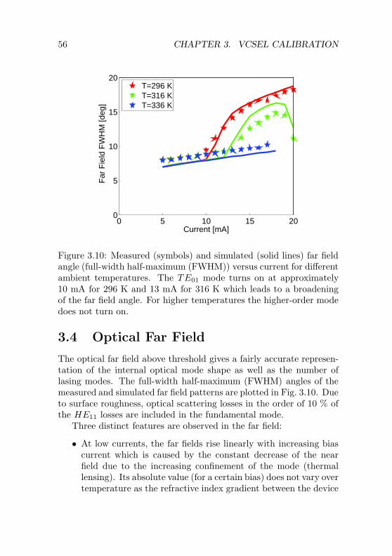
56 CHAPTER 3. VCSEL CALIBRATION
0 5 10 15 200
5
10
15
20
Current [mA]
Far
Fie
ld F
WH
M [d
eg]
T=296 KT=316 KT=336 K
Figure 3.10: Measured (symbols) and simulated (solid lines) far fieldangle (full-width half-maximum (FWHM)) versus current for differentambient temperatures. The TE01 mode turns on at approximately10 mA for 296 K and 13 mA for 316 K which leads to a broadeningof the far field angle. For higher temperatures the higher-order modedoes not turn on.
3.4 Optical Far Field
The optical far field above threshold gives a fairly accurate represen-tation of the internal optical mode shape as well as the number oflasing modes. The full-width half-maximum (FWHM) angles of themeasured and simulated far field patterns are plotted in Fig. 3.10. Dueto surface roughness, optical scattering losses in the order of 10 % ofthe HE11 losses are included in the fundamental mode.
Three distinct features are observed in the far field:
• At low currents, the far fields rise linearly with increasing biascurrent which is caused by the constant decrease of the nearfield due to the increasing confinement of the mode (thermallensing). Its absolute value (for a certain bias) does not vary overtemperature as the refractive index gradient between the device

3.5. SUMMARY 57
center and the peripheral areas of the device stays approximatelyconstant for different ambient temperatures.
• The turn-on of the higher-order TE01 mode results in a sud-den increase of the FWHM angle (e.g. for room temperature atapproximately 10 mA) as the TE01 far field is wider than thatof the fundamental mode. The total far field of a multi-modedevice is given by the superposition of the individual far fieldsper mode. As soon as the higher-order mode reaches thresholdthe modes compete for the carriers in the reservoir and, hence,for stimulated emission. This leads to a lowering of the funda-mental output power and to an increase in the output power ofthe higher-order mode which is visible in the strong influence ofthe TE01 mode on the far field.
• The bias current at which the higher-order mode turns on in-creases with temperature (TE01-turn-on at 10 mA for 296 Kand 13 mA for 316 K), which will be explained in Section 4.2.
3.5 Summary
In this chapter, the calibration of the electro-opto-thermal simula-tions of a long-wavelength VCSEL with tunnel junction to a set oftemperature-dependent device characteristics was presented. In a firststep, the material gain tables were calculated from microscopic theory.The real part of the refractive index due to a change in gain was ob-tained from the Kramers-Kronig transformation of the material gain.Both, material gain and the resulting refractive index change are in-put parameters to the device simulator. In the next step, the actualcalibration of the VCSEL characteristics was presented. The voltage-current and power-current characteristics show good agreement withmeasurements. The wavelength was calibrated over temperature andcurrent, for the fundamental and first higher-order mode. The far fieldshows the turn-on of the higher-order mode quite clearly and a goodcorrespondence between simulations and measurements was achieved.


Chapter 4
Self-Consistent
Electro-Opto-Thermal
Simulation: VCSEL
Analysis
In this chapter, the long-wavelength VCSEL design which was cal-ibrated to measurements in Chapter 3 is analyzed and optimized.First, the thermal behavior of the investigated VCSEL over injectioncurrent is discussed, i.e. the threshold characteristics as well as ther-mal power roll-over are analyzed. The influence of the temperatureand carrier distributions on the optical far field is examined. A specialemphasis is laid on the optical mode switching which is investigated indetail. Furthermore, characteristic parameters of the device are ana-lyzed. The chapter closes with a design study aiming at improving thesingle-mode output power of the device over a range of temperatures.
59

60 CHAPTER 4. VCSEL ANALYSIS
4.1 Thermal Analysis of Lasing Charac-
teristics
The poor heat dissipation through the DBRs as well as the electric re-sistance of interfaces and bulk layers lead to a pronounced self-heatingof the active area - which in turn results in a strong thermal depen-dence of the device characteristics. Additionally, the thermal con-ductivity of InP-based compounds used in long-wavelength VCSELsis reduced (due to the ternary and quaternary alloys) as opposed to(short-wavelength) AlGaAs VCSELs. For a proper device design it isimportant to understand the VCSEL’s temperature dependencies.
One important VCSEL property is the material gain which showsa strong temperature dependence and substantially influences theVCSEL characteristics. The output characteristics can be - to someextend - governed by the offset between the lasing wavelength andthe gain peak. A negative gain-mode offset (the gain peak is blue-shifted with respect to the mode) is commonly applied in order toimprove high-temperature characteristics [83, 94]. The red-shift ofthe gain peak with increasing temperature is stronger than the shiftof the cavity mode1. The specific detuning of the device will counter-act the tendency of a decreasing material gain with increasing tem-perature (assuming a fixed carrier density). Hence, in a (restricted)temperature range, the material gain at lasing wavelength will actu-ally increase with higher temperatures (Figs. 4.1 and 4.3) before itdecreases again at more elevated temperatures. Thus, the materialgain and the temperature behavior at high temperatures is improvedby choosing a strong negative detuning - but at the expense of themaximum achievable output power at lower temperatures.
The lasing regime of a VCSEL can be classified in three regions:lasing threshold, operation regime and thermal roll-over (Fig. 4.4).
4.1.1 Lasing Threshold
In Fig. 4.5 the evolution of the electron carrier density in a cen-ter quantum well over injection current is depicted for 296 K and
1In this specific device, the gain shift equals 0.4 nm/K and the wavelength shiftresults in 0.1 nm/K, compare Fig. 4.2.
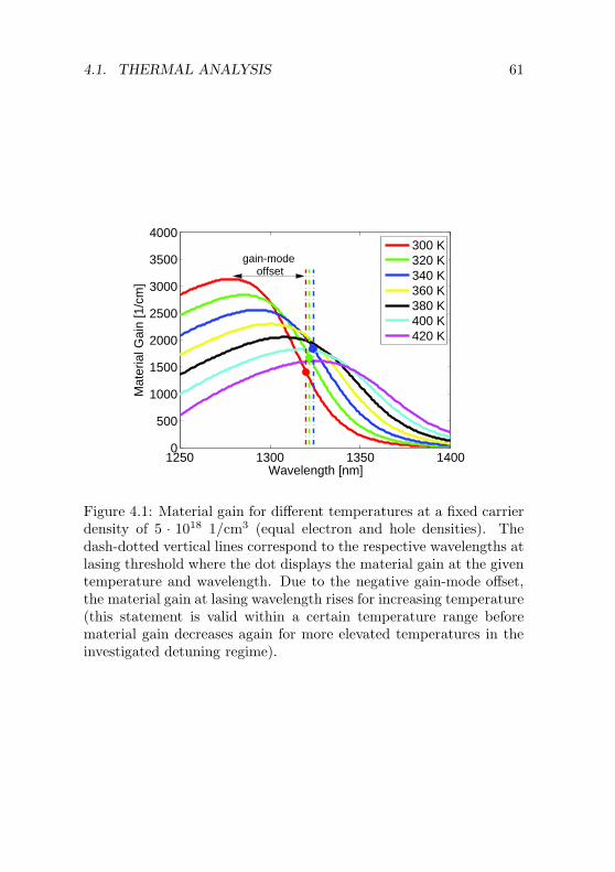
4.1. THERMAL ANALYSIS 61
1250 1300 1350 14000
500
1000
1500
2000
2500
3000
3500
4000
Wavelength [nm]
Mat
eria
l Gai
n [1
/cm
]
gain-modeoffset
300 K320 K340 K360 K380 K400 K420 K
Figure 4.1: Material gain for different temperatures at a fixed carrierdensity of 5 · 1018 1/cm3 (equal electron and hole densities). Thedash-dotted vertical lines correspond to the respective wavelengths atlasing threshold where the dot displays the material gain at the giventemperature and wavelength. Due to the negative gain-mode offset,the material gain at lasing wavelength rises for increasing temperature(this statement is valid within a certain temperature range beforematerial gain decreases again for more elevated temperatures in theinvestigated detuning regime).

62 CHAPTER 4. VCSEL ANALYSIS
200 250 300 350 400 4501240
1260
1280
1300
1320
1340
Temperature [K]
Wav
elen
gth
[nm
]
room temperaturedetuning
zero gain-mode offset
gain peak wavelengthlasing wavelength
Figure 4.2: Wavelength shift of the gain peak as well as the cav-ity wavelength at threshold versus temperature, both extracted fromsimulation. While the wavelength of the gain peak increases with0.4 nm/K (due to band gap shrinkage) the cavity wavelength increaseswith 0.1 nm/K (due to the temperature-dependence of the refractiveindex). Zero gain-mode offset - which is characterized by the crossingof the two curves - is reached at approximately 440 K. The room-temperature detuning is around 45 nm. The gain peak is extractedfor constant carrier densities of 5 · 1018 1/cm3.

4.1. THERMAL ANALYSIS 63
200 250 300 350 400 4500
1000
2000
3000
4000
5000
Temperature [K]
Mat
eria
l Gai
n [1
/cm
]
maximumthreshold gain
zero gain-mode offset
peak gainthreshold gain
Figure 4.3: Maximum (peak) material gain as well as material gainat threshold wavelength for different temperatures at a fixed carrierdensity of 5 ·1018 1/cm3 (equal electron and hole densities). The gainpeak decreases at a rate of -14 1/(cmK) with increasing temperature.The maximum threshold material gain at lasing wavelength (assumingconstant threshold density) is reached at 360 K while the zero mode-gain offset is situated at 440 K.

64 CHAPTER 4. VCSEL ANALYSIS
0 5 10 15 200
0.5
1
1.5
2
2.5
3
3.5
4
Out
put P
ower
[mW
]
Current [mA]
Total output powerHE
11 output power
TE01
output power
TE threshold
Opera
tion
regim
eThermal roll-over
thresholdLasing
01
Figure 4.4: Output power versus injection current at 296 K. The totaloutput power (solid line) is given by the power contributions of thefundamental HE11 (dashed line) and the higher-order TE01 (dash-dotted line) modes. The lasing threshold, operating regime as well asthe thermal roll-over regime are indicated.

4.1. THERMAL ANALYSIS 65
1
1.5
2
2.5
3
3.5
4
4.5
5
5.5x 10
18
01
23
45
510
1520
2
4
6
x 1018
Current [m
A]
Ele
ctro
n D
ensi
ty [1
/cm
3 ]
20Ele
ctro
n D
ensi
ty [1
/cm
3 ]
01
23
45
510
15
2
4
6
x 1018
Current [m
A]
Radius [ m]
Radius [ m]
296 K
336 K
Figure 4.5: The evolution of the electron density versus injection cur-rent in the middle quantum well at room temperature (top) and atan ambient temperature of 336 K (bottom). The x-axis shows thelateral distance from the symmetry axis of the device, the y-axis theinjection current and the z-axis the carrier density.

66 CHAPTER 4. VCSEL ANALYSIS
-2000
-1000
0
1000
2000
3000
4000
01
23
45
510
1520
-2000
0
2000
4000
Current [m
A]
Mat
eria
l Gai
n [1
/cm
]
01
23
45
510
1520
-2000
0
2000
4000
Current [m
A]
Mat
eria
l Gai
n [1
/cm
]
Radius [ m]
Radius [ m]
296 K
336 K
Figure 4.6: The evolution of material gain versus injection currentin the middle quantum well at room temperature (top) and at anambient temperature of 336 K (bottom). The x-axis shows the lateraldistance from the symmetry axis of the device, the y-axis the injectioncurrent and the z-axis the material gain.

4.1. THERMAL ANALYSIS 67
336 K. Generally, the QW carrier density rises until mode gain equalsmode loss and, hence, the (fundamental) mode reaches lasing thresh-old (around an injection current of 3-4 mA, compare Fig. 3.8). Dueto the specific detuning configuration of the device, threshold gainat elevated temperatures may be reached at smaller carrier densitiesthan for lower temperatures - because of higher mode gain at a givencarrier density (Fig. 4.3) as well as smaller losses (see Fig. 4.18). Thecorresponding material gain over injection current is shown in Fig. 4.6for ambient temperatures of 296 K and 336 K. Even though thresholdgain at 336 K is lower than for 296 K - where one might assume thatthreshold should be reached at lower carrier densities - does not meanthat the laser turn-on takes place at a lower injection current with ele-vated temperatures. As the Auger coefficient (2.56) rises with increas-ing temperature, an increased number of carriers gets lost at highertemperatures due to the augmented Auger recombination (Fig. 4.7).This results in a higher threshold current at 336 K than for roomtemperature.
Generally, it is assumed that the minimum in threshold current co-incides with the overlap of lasing wavelength and gain peak [51, 95, 96].This design rule is commonly employed for short-wavelength AlGaAs-based VCSEL. This concept does not hold, however, for InP-basedlong-wavelength VCSELs which are strongly influenced by Auger andfree carrier recombination [97, 98]. A zero gain-mode offset at thresh-old would be reached at approximately 440 K (Fig. 4.2). In the ana-lyzed device, the minimum threshold current is achieved around 310 Kwhich corresponds to a negative detuning of approximately 40 nm atthis temperature2. Due to the strong detuning, the maximum gainseen by the optical cavity mode is not achieved at zero gain-modeoffset but at lower temperatures (and, hence, at off-peak positionsin the gain curve, compare Fig. 4.3). Furthermore, the temperature-dependence of the Auger-coefficient increases the threshold currentat higher temperatures above average. Thus, the threshold-minimumis shifted towards lower temperatures and, hence, towards a negativegain-mode offset.
2The Ith-minimum of the measured and simulated characteristics (Fig. 3.8)differ by 6 nm. As the analysis presented in this section is entirely based onsimulation results, the corresponding Ith,min-value, which was extracted fromsimulation, is used.

68 CHAPTER 4. VCSEL ANALYSIS
0
0.5
1
1.5
01
23
45
510
1520
0
1
Current [m
A]
Aug
er R
ecom
bina
tion
[10
1/
(cm
s)]
329
Radius [ m]
01
23
45
510
1520
0
1
Current [m
A]
Aug
er R
ecom
bina
tion
[10
1/
(cm
s)]
Radius [ m]
296 K
336 K
329
Figure 4.7: The evolution of Auger recombination versus injectioncurrent in the middle quantum well at room temperature (top) andat an ambient temperature of 336 K (bottom). The x-axis shows thelateral distance from the symmetry axis of the device, the y-axis theinjection current and the z-axis the Auger recombination rate.

4.1. THERMAL ANALYSIS 69
4.1.2 Operation Regime
The operation regime is described by the (linear) power-current char-acteristic which exists above threshold and below thermal roll-over.The distribution of the bound carriers (Fig. 4.5) within the quan-tum well is determined by carrier recombination and drift-diffusionprocesses in the QW as well as current confinement measures in thecavity. Lasing threshold is characterized by the domination of stimu-lated recombination. The area where this process prevails is given bythe optical mode shape. As the fundamental (Gaussian-shaped) HE11
mode starts lasing first this leads to a significant reduction of carriersin the center of the quantum well with increasing injection current.This effect is called spatial hole burning (SHB). Furthermore, thecurrent aperture also significantly influences the QW carrier profile,which leads to current crowding along the edges of the aperture and,hence, to a higher carrier density in these off-center locations. Withthe entry into the lasing regime also the optical losses start to decline(see Fig. 4.18) which directly results in a reduced lasing gain.
At room temperature, maximum spatial hole burning around thedevice’s symmetry axis takes place around 10 mA, shortly before theon-set of the higher-order TE01 mode. The higher-order mode dis-plays its maximum intensity at an off-center location while the fun-damental mode has its maximum in the device center (along the sym-metry axis), compare Fig. 4.15. The on-set of the TE01 mode resultsin an increase of the slope efficiency (compare Figs. 3.7 and 4.4) asthe higher-order mode partly accesses a carrier reservoir (in the off-center location) which was not accessible to the fundamental mode.Hence, multi-mode lasing comes along with increased stimulated emis-sion in the off-center locations (around 3 µm in lateral direction) andan increased reduction of carriers in these areas which is visible asmulti-mode spatial hole burning. Furthermore, the two modes alsoshare part of the carrier reservoir towards the device center, compet-ing for stimulated emission in this area. This results in a decrease ofthe optical output power of the fundamental mode and an increase ofthe the power in the higher-order mode (Fig. 4.4).

70 CHAPTER 4. VCSEL ANALYSIS
300
320
340
360
380
400
420
440
01
23
45
510
1520
350
400
450
Current [m
A]
Tem
pera
ture
[K]
01
23
45
510
1520
300
350
400
Current [m
A]
Tem
pera
ture
[K]
Radius [ m]
Radius [ m]
296 K
336 K
Figure 4.8: The course of temperature (self-heating) versus injectioncurrent in the middle quantum well at room temperature (top) andat an ambient temperature of 336 K (bottom). The x-axis shows thelateral distance from the symmetry axis of the device, the y-axis theinjection current and the z-axis the local temperature.

4.2. OPTICAL MODE SELECTIVITY 71
4.1.3 Thermal Roll-Over
Roll-over of the optical output power is described by a divergencefrom the quasi linear L-I-behavior seen in the typical operation regimewhich results in a decrease of the output power with increasing injec-tion current. The thermal roll-over regime will be exemplarily ana-lyzed at an ambient temperature of 336 K. At this temperature, themaximum output power is reached at an injection current of 11 mA.
The roll-over is commonly seen as a thermal effect [99, 100]: Tem-perature steadily rises within the device due to self-heating (Fig. 4.8)which continuously increases the Auger coefficient (Fig. 4.7). Thissupports a decrease of the carriers in the QW active region due toincreased nonradiative recombination. Above a certain temperaturethe negative gain-mode offset will not provide any relief: with risingtemperature material gain starts to decrease again. This, in turn,brings about a rise in carrier density in order to keep up thresholdgain. Consequently, this leads to an increase in temperature as wellas recombination losses, foremost due to enhanced Auger recombina-tion3. Additionally, the increased carrier densities lead to a rise inlosses due to FCA.
At room temperature, the roll-over regime is entered around 17 mAwhich is also characterized by an increase in Auger recombination aswell as carrier density. The bias current at which the roll-over regimesets in generally decreases with ambient temperature. This can beexplained by enhanced Auger recombination as well as decreasing ma-terial gain (at constant carrier density) with increasing temperature.
4.2 Optical Mode Selectivity
For the design of single- and multi-mode devices, it is crucial to un-derstand the process of mode selectivity and to model the underlyingmechanisms correctly. In the following, the components influencingthe far field are identified, the influence of the current aperture on theoptical far field is shown and the delayed turn-on of the higher-ordermode with increasing temperature is analyzed.
3This is not only caused by the increase of the (temperature-dependent) Augercoefficient but also the increase in carrier density.

72 CHAPTER 4. VCSEL ANALYSIS
0 5 10 15 200
5
10
15
20
15 mA
Current [mA]
Far
Fie
ld F
WH
M [d
eg]
n0
n
Tn
Gainn
FCAn
0n
Tn
0n
Gain
n0
n0
n
FCA
Figure 4.9: Simulation of the far field angle (full-width half-maximum)versus bias current. The effects of gain, temperature and free carrierabsorption included in the refractive index on the far field are plot-ted. The cold-cavity solution is shown for reference. All simulationsare performed at room temperature (296 K). The dash-dotted line at15 mA visualizes the injection current at which the refractive indexextraction is performed in Fig. 4.10.
4.2.1 Impact of Carrier and Temperature Depen-
dencies of the Refractive Index
To better understand the underlying mode-selective mechanisms theeffects of temperature, carriers and gain (2.67, 2.69, 2.73) on the realpart of the refractive index and, hence, on the far field are investi-gated and visualized in a simulation study. The input parametersto the refractive index model were calibrated through the calibrationpresented in Chapter 3.3: The value of αT is taken from literature.The impact of FCA can be calibrated from the external quantum effi-ciency extracted from the L-I-curve (Fig. 3.7) and the gain parametersare obtained from the Kramers-Kronig transform of the material gainin Section 3.2.

4.2. OPTICAL MODE SELECTIVITY 73
0 2 4 6 8
3.65
3.7
3.75
3.8
Ref
ract
ive
Inde
x [1
]
n0
n
Tn
0n
Gain
n0
n
FCA
n0
Radius [ m]
Figure 4.10: Simulation of the refractive index profile in the centerquantum well in lateral direction from the symmetry axis of the device.The impact of the distributions of carrier density, temperature andgain on the refractive index profile is visualized. Temperature andfree carrier absorption alter the refractive indices in the entire device,while the effect of gain is only present in the active region. Thematerial refractive index n0 is plotted for reference. All simulationsare performed at room temperature (296 K) and 15 mA.

74 CHAPTER 4. VCSEL ANALYSIS
First of all, each effect is investigated individually: Fig. 4.10 showsthe lateral refractive index profile in the middle QW of the simulateddevice. The resulting far field is depicted in Fig. 4.9. It has to benoted that the impact of gain on the refractive index is only present inthe active region, while temperature as well as free carrier absorptionaffect the refractive indices in the entire device. This relativizes theabsolute values of the individual contributions of temperature, gainand FCA on the refractive index shown in Fig. 4.10.
Cold-cavity solution. The cold-cavity solution of the optical modepattern is influenced by the distribution of the material refractiveindex n0 as well as the geometry of the device. Taking this solutionas an input for the electro-opto-thermal calculations will result in nochange of the optical mode pattern over injection current and, hence,lead to a constant (single-mode) far field over temperature.
Temperature dependence. The temperature rise in the devicecenter due to self-heating leads to a continuous rise in refractive indexwith increasing bias current. The temperature decreases towards theperiphery of the device which results in a gradient of the refractiveindices in lateral direction. This leads to a focussing of the nearfield (thermal lensing) and, thus, yields a continuous expansion of theoptical far field with increasing injection current. Fig. 4.9 shows thatthe - exclusive - inclusion of thermal lensing results in a linear increaseof the FWHM angle of the far field with increasing current until theTE01 mode starts lasing at high injection currents.
Carrier dependence. The carrier-dependencies of the refractiveindex due to gain and free carrier absorption, ∆n′
Gain and ∆n′
FCA,inversely follow the carrier distribution in the active region (Fig. 4.10)which results in a higher refractive index at the periphery than in thedevice center. The minimum in the refractive index distribution iscaused by current crowding and the increase towards the device cen-ter originates from spatial hole burning. Due to the smaller refractiveindex in the device center, the lateral refractive index contrast is de-creased which deteriorates the waveguide. This leads to a defocussedoptical near field and, thus, a smaller far field angle than for the case

4.2. OPTICAL MODE SELECTIVITY 75
where only the material refractive index n0 is considered. This be-havior can be described as an anti-guiding effect. Above threshold thefar field angle remains approximately constant over injection current.Thus, the refractive index changes due to free carrier absorption andgain, both, result in a negative offset of the far field angle (Fig. 4.9).
Resulting far field. The simultaneous inclusion of all componentsin the real part of the refractive index (n0 +∆n′
T +∆n′
Gain +∆n′
FCA)leads to a similar behavior as if only the temperature effect on therefractive index is considered: The overall far field linearly increaseswith rising bias current. Compared to the temperature effect alone,n0 + ∆n′
T , the optical mode is defocussed by the carrier dependentcomponents, ∆n′
Gain and ∆n′
FCA. This anti-guiding effect causes thehigher-order mode to be slightly less confined in lateral direction and,hence, witness less gain (but approximately the same losses). Thisresults in an increased turn-on current for the TE01 mode comparedto the sole inclusion of the temperature effect.
Near Field Analysis. The near fields plotted in Fig. 4.11 show themode dynamics versus injection current for different depth of model-ing of the real part of the refractive index: a comparison of only thebackground refractive index n0 (cold-cavity), inclusion of the temper-ature effect, n0+∆n′
T , and of all effects, n0+∆n′
T +∆n′
Gain+∆n′
FCA,shows the differences on the optical near field and the mode dynamics.The turn-on of the TE01 mode is characterized by the formation ofoff-center high intensity lobes at higher injection currents. Calculat-ing the optical mode profile only for the cold-cavity solution, wherethe optics are not re-solved with increasing injection current, leads toa wrong current-mode dependence as temperature and carrier relatedeffects on the refractive index and, thus, the optical mode are notaccounted for. This results in an incorrect picture of the optical modepattern over injection current.
This analysis shows that - in order to simulate single-mode be-havior as well as effects on the far field correctly - the influence oftemperature and carriers on the real part of the refractive index haveto be considered as these properties have a significant impact on the

76 CHAPTER 4. VCSEL ANALYSIS
-50
5 5
10
15
0
2
Opt
ical
Nea
r F
ield
Inte
nsity
[a.u
.]
0
0.5
1
1.5
2
2.5
3
3.5
Cur
rent
[mA]
Radius [ m]
(a)
-50
5 5
10
15
0
2
Cur
rent
[mA]
Opt
ical
Nea
r F
ield
Inte
nsity
[a.u
.]
(b)
-50
5 5
10
15
0
2
Opt
ical
Nea
r F
ield
Inte
nsity
[a.u
.]
Cur
rent
[mA]
(c)
Radius [ m]Radius [ m]
Figure 4.11: Simulated near field patterns versus injection currentat room temperature (in a lateral cut through the near field center).The x-axis shows the lateral distance from the symmetry axis of thedevice, the y-axis the injection current and the z-axis the optical nearfield intensity. The evolution of the near field over current is shownfor (a) all implemented refractive index terms (n0 + ∆n′
T + ∆n′
Gain +∆n′
FCA), (b) the cold-cavity condition (n0) and (c) the inclusion ofthe temperature dependence of the refractive index (n0 + ∆n′
T ). Thelasing of the higher-order HE01 mode is characterized by the splittingof the near field peak.
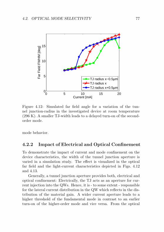
4.2. OPTICAL MODE SELECTIVITY 77
0 5 10 15 200
5
10
15
Current [mA]
Far
Fie
ld F
WH
M [d
eg]
TJ radius x−0.5µmTJ radius xTJ radius x+0.5µm
Figure 4.12: Simulated far field angle for a variation of the tun-nel junction-radius in the investigated device at room temperature(296 K). A smaller TJ-width leads to a delayed turn-on of the second-order mode.
mode behavior.
4.2.2 Impact of Electrical and Optical Confinement
To demonstrate the impact of current and mode confinement on thedevice characteristics, the width of the tunnel junction aperture isvaried in a simulation study. The effect is visualized in the opticalfar field and the light-current characteristics depicted in Figs. 4.12and 4.13.
Generally, a tunnel junction aperture provides both, electrical andoptical confinement: Electrically, the TJ acts as an aperture for cur-rent injection into the QWs. Hence, it is - to some extent - responsiblefor the lateral current distribution in the QW which reflects in the dis-tribution of the material gain. A wider current aperture leads to ahigher threshold of the fundamental mode in contrast to an earlierturn-on of the higher-order mode and vice versa. From the optical

78 CHAPTER 4. VCSEL ANALYSIS
0 5 10 15 200
0.5
1
1.5
2
2.5
3
3.5
4
4.5
Out
put P
ower
[mW
]
Current [mA]
TJ radius x-0.5 mTJ radius xTJ radius x+0.5 m
HE11
TE01
Figure 4.13: Simulated light-current characteristic for a variation ofthe tunnel junction-radius at room temperature (296 K) in the inves-tigated device. Solid lines depict the total output power while thedashed lines show the HE11 and TE01 power components.

4.2. OPTICAL MODE SELECTIVITY 79
point of view, the higher refractive index of the tunnel junction ma-terial results in a slightly different refractive index contrast in lateraldirection depending on the TJ diameter and, hence, influences thewidth of the overall far field: a wider TJ aperture leads to a smallerfar field angle and vice versa. The better current confinement atsmaller aperture sizes results in an increased slope efficiency of thefundamental HE11 mode while wider current apertures increase theslope efficiency of the higher-order TE01 mode. The latter is alsothe reason for the faster broadening of the far field shortly after theturn-on of the TE01 mode. Furthermore, a smaller aperture leads toincreased self-heating. This results in a steeper increase of the farfield angle for small TJ aperture sizes with increasing current as wellas an earlier roll-over of the optical output power. For the smallestaperture size in Fig. 4.12, the decrease in the higher-order far field athigh currents is determined by the earlier on-set of the roll-over dueto increased self-heating.
4.2.3 Mode Dynamics
In order to understand the temperature-dependent threshold of thehigher-order TE01 mode, once again the interplay between carrier-density profile and mode gain in the quantum well region has to beinvestigated. The maximum of the optical intensity of the higher-order mode does not coincide with the device axis. As describedin Section 4.1, the bound carrier distribution within the quantumwell active region is determined by carrier recombination and drift-diffusion processes in the QW as well as current confinement measuresin the cavity. The carrier density rises with temperature (Fig. 4.14) asthreshold gain has to be reached. From the TJ aperture radially out-ward, the carrier density decreases towards the periphery of the device- an effect which is nearly constant over temperature4 (Fig. 4.14). Thisleads to a decrease in the material gain (increase in absorption) in thisperipheral area with increasing temperature (Fig. 4.15): the thermallyinduced band gap shrinkage increases absorption over temperature inthe low carrier densities region at these off-center locations. Due to
4The slight decrease in carrier density over temperature in the peripheral areaof the device comes from the lowered carrier mobilities at high temperatures and,hence, smaller drift-diffusion terms.

80 CHAPTER 4. VCSEL ANALYSIS
0 2 4 6 8
1
2
3
4
5
x 1018
QW
Ele
ctro
n D
ensi
ty [1
/cm
3
296 K316 K336 K
Radius [ m]
]
Figure 4.14: Simulated electron carrier density in the center quantumwell along the lateral direction from the symmetry axis of the devicefor different ambient temperatures as well as a bias current of 15 mA.

4.3. DEVICE ANALYSIS 81
0 2 4 6 80
1
2
3
4
Opt
ical
Inte
nsity
[a.u
.]
0
1000
2000
3000296 K316 K336 K
-3000
-2000
-1000
Mat
eria
l Gai
n [1
/cm
]
Radius [ m]
Figure 4.15: Left axis: simulated optical intensity of the fundamentalHE11 (solid lines) and first higher-order TE01 (dashed lines) mode.Right axis: simulated material gain. The transition between gain andabsorption regime is marked by the dash-dotted line. All quantitiesare displayed along the lateral direction from the symmetry axis ofthe device in the center QW for different temperatures as well as abias current of 15 mA.
the specific mode confinement the decrease in material gain/increasein absorption only affects the (outer lobes of the) TE01 mode (refer toFig. 4.15). Therefore, the turn-on current for the TE01 mode increasesat elevated ambient temperatures.
4.3 Device Analysis
In the case of the microscopic device model used in this work theinput parameters are the geometry of the device and the respective(physical) material parameters - all other device characteristics arecalculated self-consistently. This stands in contrast to simulationsusing rate equations where a number of important input parametershave to be guessed. These parameters include material gain g and

82 CHAPTER 4. VCSEL ANALYSIS
differential gain dg/dN , confinement factor Γ, and photon lifetimeτS , just to name a few. In such zero-dimensional simulations theseparameters are normally set to constant (temperature and spectrallyindependent) values which leads to a significant error due to the factthat many of these parameters are dependent on operation wavelengthor temperature (let alone the loss of information due to the reduceddimensionality of the model).
In this section, a number of device characteristics are extractedfrom the calibrated model and their dependencies are shown - someof these terms are also input to the rate equation model.
Differential material gain. The differential material gain for elec-trons and holes is extracted from the calculated material gain pre-sented in Chapter 3 and is depicted in Fig. 4.16. The total effectivedifferential material gain dg/dN is the sum of the two contributionsby electrons and holes, dg/dn and dg/dp. Generally, the effective dif-ferential gain decreases with increasing density (for a wide wavelengthrange) and tends to saturate with high carrier densities.
At low carrier densities the contribution from electrons commonlydominates the effective differential gain as the electron effective massis much smaller than the one of holes in InP. This results in fastchanges of the quasi-Fermi level. At high carrier densities the holedifferential gain plays the important role: Transitions of the secondconduction band subband at different spectral positions decrease theelectron differential gain.
For the specific detuning of the investigated device, the hole differ-ential gain lies at slightly higher values than the electron differentialgain. The electron differential gain only provides a constant offset -independent of the carrier density. Only changes in the hole densitywill lead to a variation of the total differential gain in this detuningconfiguration which results in an increase of the total differential gaindg/dN with higher carrier densities.
Optical confinement factor. The optical confinement factor Γ isdefined as the fraction of the integrated field distribution overlapping

4.3. DEVICE ANALYSIS 83
1250 1300 1350
0
5
10
15
20x 10
-16
Wavelength [nm]
Diff
eren
tial M
ater
ial G
ain
dg/d
p [c
m2 ]
8.2e17 1/cm1.5e18 1/cm2.7e18 1/cm5.0e18 1/cm
1250 1300 1350
0
5
10
15
20x 10
-16
Wavelength [nm]
Diff
eren
tial M
ater
ial G
ain
dg/d
n [c
m2 ]
8.2e17 1/cm1.5e18 1/cm2.7e18 1/cm5.0e18 1/cm
Figure 4.16: Differential material gain for electrons (top) and holes(bottom) at 296 K. Note that the plots for both, dg/dn and dg/dp,display the same y-axis range for better comparability of the absolutevalues of the characteristics.

84 CHAPTER 4. VCSEL ANALYSIS
0 5 10 15 200.0165
0.017
0.0175HE
11
TE01
Opt
ical
Con
finem
entfa
ctor
[1]
Current [mA]
296 K316 K336 K
Figure 4.17: Optical confinement factor Γ over injection current fordifferent ambient temperatures. Solid lines: HE11 mode, dashed lines:TE01 mode.
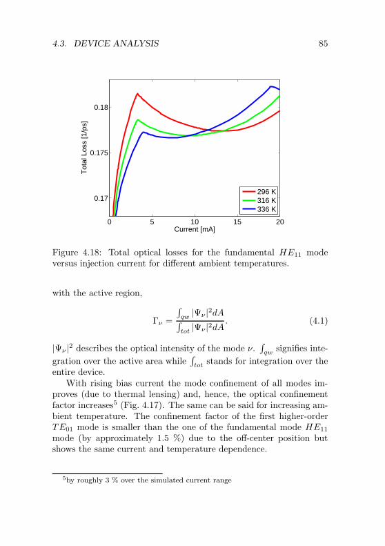
4.3. DEVICE ANALYSIS 85
0 5 10 15 20
0.17
0.175
0.18
Tot
al L
oss
[1/p
s]
Current [mA]
296 K316 K336 K
Figure 4.18: Total optical losses for the fundamental HE11 modeversus injection current for different ambient temperatures.
with the active region,
Γν =
∫
qw |Ψν |2dA∫
tot |Ψν |2dA. (4.1)
|Ψν |2 describes the optical intensity of the mode ν.∫
qw signifies inte-
gration over the active area while∫
tot stands for integration over theentire device.
With rising bias current the mode confinement of all modes im-proves (due to thermal lensing) and, hence, the optical confinementfactor increases5 (Fig. 4.17). The same can be said for increasing am-bient temperature. The confinement factor of the first higher-orderTE01 mode is smaller than the one of the fundamental mode HE11
mode (by approximately 1.5 %) due to the off-center position butshows the same current and temperature dependence.
5by roughly 3 % over the simulated current range

86 CHAPTER 4. VCSEL ANALYSIS
Total optical losses. The total optical losses (2.38) are the in-verse of the photon life time τS and are given by the device structure(e.g. mirror (out-coupling) or diffraction losses) as well as free carrierlosses. The total losses of the fundamental HE11 mode are depictedin Fig. 4.18. Below threshold the carrier densities rise with increas-ing current and, hence, losses increase due to increased free carrierabsorption.
From simplified models (such as rate-equations) we expect the car-rier density to approximately clamp above threshold, leading to a con-stant material gain at constant losses [10]. As was shown earlier in thischapter, this is not the case in a real device (compare Fig. 4.5): Abovethreshold, the carrier density might even decrease leading to reducedFCA - an effect which is more pronounced at lower temperatures. Fur-thermore, the increase of the refractive index with self-heating resultsin a reduction of the optical losses. Around roll-over, carrier densitiesstart to rise again and, thus, total losses increase once more due toincreased free carrier absorption. This point is reached earlier withincreasing ambient temperature.
Generally, the losses below roll-over decrease with increasing am-bient temperature due to the increase of the refractive index withtemperature.
Wall-plug efficiency. The wall-plug efficiency (also power-conver-sion efficiency) (Fig. 4.19) is defined as the ratio of optical outputpower to injected electrical power
ηtot =Pout
Pin=
P
IV. (4.2)
It is a measure of the quality of the device and also stands for the con-version of electrical power into heat. In the short-wavelength range,wall-plug efficiencies as high as 57 % have been reported [30] whichwere achieved with multi-mode devices. The long-wavelength VCSELsection is trailing behind with less than 25 % conversion efficiencyachieved for a multi-mode VCSEL. Naturally, single-mode deviceshave lower wall-plug efficiencies which lie in the range of 15 % inthe long-wavelength regime [101, 102]. In the investigated device,the power conversion efficiency reaches its (room temperature) peak

4.3. DEVICE ANALYSIS 87
0 5 10 15 200
2
4
6
8
10
12
Pow
er C
onve
rsio
n E
ffici
ency
[%]
Current [mA]
0 5 10 15 20290
330
370
410
450
0 5 10 15 20290
330
370
410
450
Max
imum
Act
ive
Reg
ion
Tem
pera
ture
[K]
296 K336 K
Figure 4.19: Simulated power conversion efficiency (wall-plug effi-ciency) and maximum active region temperature
value of more than 10 % shortly after threshold and deteriorates forhigher current values due to increased temperature related loss mech-anisms. The turn-on of the TE01 mode around 10 mA causes thekink (increase in efficiency) in the room temperature conversion effi-ciency. Compared to measurements, the maximum power conversionefficiency is overestimated in simulation due to the slightly higherslope efficiency.
Optical external efficiency. The optical external efficiency (slopeefficiency) ηd relates the differential change in output power versusbias current and is given by the slope of the LI-curve (Fig. 3.7). It isdefined as
ηd = ηiLout
Ltot, (4.3)
with the (electrical) injection efficiency ηi, out-coupling losses Lout
and total losses Ltot. Ideally, ηd is constant meaning that the effi-ciency with which the laser converts electrons applied at the contact
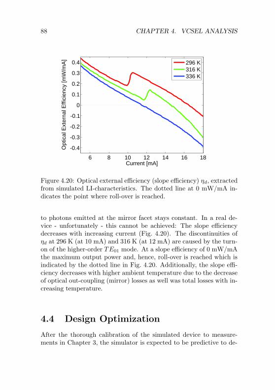
88 CHAPTER 4. VCSEL ANALYSIS
6 8 10 12 14 16 18
-0.4
-0.3
-0.2
-0.1
0
0.1
0.2
0.3
0.4
Current [mA]
Opt
ical
Ext
erna
l Effi
cien
cy [m
W/m
A]
296 K316 K336 K
Figure 4.20: Optical external efficiency (slope efficiency) ηd, extractedfrom simulated LI-characteristics. The dotted line at 0 mW/mA in-dicates the point where roll-over is reached.
to photons emitted at the mirror facet stays constant. In a real de-vice - unfortunately - this cannot be achieved: The slope efficiencydecreases with increasing current (Fig. 4.20). The discontinuities ofηd at 296 K (at 10 mA) and 316 K (at 12 mA) are caused by the turn-on of the higher-order TE01 mode. At a slope efficiency of 0 mW/mAthe maximum output power and, hence, roll-over is reached which isindicated by the dotted line in Fig. 4.20. Additionally, the slope effi-ciency decreases with higher ambient temperature due to the decreaseof optical out-coupling (mirror) losses as well was total losses with in-creasing temperature.
4.4 Design Optimization
After the thorough calibration of the simulated device to measure-ments in Chapter 3, the simulator is expected to be predictive to de-

4.4. DESIGN OPTIMIZATION 89
sign variations in the calibrated material system. Improving a device’sperformance is always a challenging task. Multi-dimensional physics-based simulations provide a good framework for device optimization- shortening the time- and cost-intensive experimental improvementprocess.
Design variations. In simulation, a series of design variations wasperformed for a range of ambient temperatures. The effects on theL-I-V characteristics are analyzed for two different temperatures,namely 296 K and 336 K. Among the design variations performedthe following four yielded the most promising results (see Fig. 4.21):
• The p-type doping of a buffer layer between the TJ and QW-regions is increased which raises the electric field not only inthis altered layer but also in the adjacent TJ-region. This mea-sure results in a higher tunneling rate (see (2.58)) and, hence,increased hole current into the active region. This yields an ele-vated stimulated recombination rate and, thus, leads to a higherslope efficiency. The higher doping of the buffer layer increasesthe current spreading slightly also towards off-center locationswhich leads to an earlier turn-on of the higher-order mode.
• Decreasing the (negative) detuning of the device (here by 14 nm)increases mode gain and, hence, reduces threshold current sig-nificantly (at the cost of a reduced temperature stability). TheTE01-turn-on is slightly decreased as the higher-order mode alsosees higher modal gain.
• Increasing the (degenerate) n-doping of the TJ reduces the junc-tion bias. Furthermore, the lower resistivity results in a smallerself-heating of the device which is reflected in a slightly lesspronounced thermal lense. This leads to a delayed turn-on theTE01 mode.
• By reducing the TJ-radius (in this case by 0.25 µm) the turn-on of the higher-order TE01 mode can be delayed (see alsoFig. 4.13).
Generally, the turn-on of a higher-order mode could also be influ-enced - probably more efficiently - by the introduction of mode selec-

90 CHAPTER 4. VCSEL ANALYSIS
0 2 4 6 8 10 120
1
2
3
4
5
6
Current [mA]
Out
put P
ower
[mW
]
HE11
TE01
296 K
0 2 4 6 8 10 120
0 2 4 6 8 10 120
0.8
1.6
2.4
3.2
Vol
tage
[V]
original designTJ buffer dopingdetuningTJ n-dopingTJ radius
0 2 4 6 8 10 120
1
2
3
4
5
6
Current [mA]
Out
put P
ower
[mW
]
336 K
336 K336 K336 K336 K
0 2 4 6 8 10 120
0.8
1.6
2.4
3.2original designTJ buffer dopingdetuningTJ n-dopingTJ radius
Vol
tage
[V]
Figure 4.21: Simulated light-current (left axis) and voltage-current(right axis) characteristics for different design variations at 296 K(top) and 336 K (bottom). Solid lines depict the total output powerwhile the dashed lines depict the HE11 and TE01 power components.

4.5. SUMMARY 91
tive losses rather than by the limited approach of a reduced aperturediameter. Mode selective losses can be imposed in the form of ring-shaped metallic absorbers [103] or etched surface reliefs [104, 105].These measures would make an additional processing step necessaryand, therefore, were not included in this analysis.
Improved device. By simulation, the four variations describedabove are combined into one new design which now features an im-proved tunnel junction efficiency, current confinement and injectioninto the quantum well region as well as a reduced detuning of thedevice. The improved L-I-V-characteristic is compared to the originaldesign in Fig. 4.22. The turn-on voltage is decreased while the dif-ferential resistance in the V-I-characteristic is slightly increased but- overall - the improved design still features a lower voltage per (in-jection current) bias point than the original design. The thresholdcurrent is almost halved over the entire temperature range. Further-more, the maximum single-mode output power rises by 60 % at 296 Kwhile at 336 K the maximum value of the single-mode output poweris almost doubled. The wall-plug efficiency (4.2) could be improved toa (single-mode) peak value of more than 20 % at room temperature.
The turn-on of the higher-order mode is decreased by less than1 mA. Given the big improvement in the single-mode output powerbelow the turn-on of the higher-order mode and the much loweredlasing threshold the earlier turn-on of the TE01 mode can be approved.
4.5 Summary
In this chapter, the simulations calibrated in the previous chapterwere used to analyze and optimize the design of the investigated long-wavelength VCSEL. First, the optical output characteristics over in-jection current were investigated. The evolution of threshold materialgain over temperature was shown. In a long-wavelength TJ VCSEL,the parabolic dependence of the threshold current on ambient tem-perature is dependent on the room-temperature gain-mode offset aswell as Auger recombination. It was shown that the minimum of thethreshold parabola does not coincide with the overlap of the gain peakand lasing mode. Thermal roll-over is influenced by the increase of

92 CHAPTER 4. VCSEL ANALYSIS
0 2 4 6 8 10 120
1
2
3
4
5
6
Current [mA]
Out
put P
ower
[mW
]
336 K
0 2 4 6 8 10 120
1
2
3original designimproved design
0 2 4 6 8 10 120
1
2
3
4
5
6336 K
336 K336 K336 K
0 2 4 6 8 10 120
1
2
3
0 2 4 6 8 10 120
1
Vol
tage
[V]
0 2 4 6 8 10 120
1
0 2 4 6 8 10 120
1
0 2 4 6 8 10 120
1
0 2 4 6 8 10 120
1
0 2 4 6 8 10 120
1
0 2 4 6 8 10 120
1
original designimproved design
0 2 4 6 8 10 120
1
2
3
4
5
6
Current [mA]
Out
put P
ower
[mW
]
HE11
TE01
296 K
0 2 4 6 8 10 120
1
2
3
0 2 4 6 8 10 120
1
2
3
Vol
tage
[V]
original designimproved design
Figure 4.22: Simulated light-current (left axis) and voltage-current(right axis) characteristics of the original (red) and improved (blue)VCSEL design at 296 K (top) and 336 K (bottom). Solid lines depictthe total output power while the dashed lines depict the HE11 andTE01 power components.

4.5. SUMMARY 93
the internal device temperature due to self-heating at higher injectioncurrents. This leads to augmented Auger recombination as well as areduced material gain. Subsequently, an analysis of mode-switchingbehavior was performed. The far field qualifies for this investigationas it nicely displays the mode confinement as well as the turn-on ofthe higher-order mode. The self-heating as well as the carrier distri-bution within the device have a significant impact on the far field andthe multi-mode behavior of a VCSEL through their impact on the re-fractive index. An increase in temperature leads to a confinement ofthe optical mode (thermal lensing) while an increase in carrier densitywill result in an anti-guiding of the optical field. The temperature-dependent turn-on of the higher-order mode is caused by the increasedabsorption at the off-center locations with higher temperature. Thepeak wall-plug efficiency of the investigated device was shown to bearound 10 %. The chapter closes with a design optimization. Theimpact of the TJ radius and of the detuning between gain peak andlasing mode as well as the impact of the doping concentration in thetunnel junction and in a TJ buffer layer were presented. With thesemeasures the output characteristics of the VCSEL could be signifi-cantly improved for different temperatures which resulted in an ap-proximately doubled wall-plug efficiency.

Chapter 5
Conclusion and Outlook
5.1 Major Results
In this work, a TCAD simulation tool was used for the analysis of long-wavelength vertical-cavity surface-emitting lasers. The microscopicelectro-opto-thermal simulations which were solved self-consistentlywere performed with the device simulator Synopsys Sentaurus De-vice. The investigated InP-based long-wavelength VCSEL with tunneljunction was fabricated by BeamExpress SA.
A thorough calibration of the investigated device to a series oftemperature-dependent static characteristics was performed. The suc-cessful calibration of the investigated TJ VCSEL including the opti-cal far field characteristics is unique. Based on these calibrations, asystematic analysis of the device characteristics was carried out. Par-ticular attention was paid to the turn-on and the thermal roll-overbehavior of the device. This was followed by a detailed analysis of theoptical far field and the mode behavior: The impact of temperatureand carrier distributions on the optical mode shape and, hence, the farfield was investigated. Special emphasis was laid on the multi-modebehavior (inferred from far field characteristics) of the device and thetemperature-dependence of the higher-order TE01 mode turn-on wasanalyzed. Important device characteristics were analyzed.
By simulation, the injection into the quantum well region and the
95

96 CHAPTER 5. CONCLUSION AND OUTLOOK
tunnel junction efficiency as well as the detuning between the gainpeak and lasing wavelength were improved. With these measures, notonly the single-mode output power was significantly increased over alltemperatures and the turn-on voltage decreased but also the thresholdcurrent was almost halved over the entire temperature range.
5.2 Outlook
Some open issues for further work remain:Patterned VCSEL designs breaking the rotational symmetry of
the device are becoming more popular with device designers as thisapproach facilitates polarization and lateral mode control: These de-signs include asymmetric current injection schemes [106], holey struc-tures [105, 104] or lateral photonic crystal waveguides [107]. Thecurrent simulator implementation exploits the rotational symmetrypresent in standard VCSEL designs. A three-dimensional implemen-tation applying a combination of the effective index method (EIM)for the vertical optical field and the finite element method (FEM) forthe transverse field poses a number of disadvantages such as the inac-curate calculation of losses [51, 108]. Hence, a full 3D-implementationof the wave-equation for the optical field is necessary for simulationand analysis capabilities of non-symmetric VCSEL structures.
Reliability is a big issue in the commercial VCSEL manufacturing.The lifetime of the device is not only influenced by electrostatic dis-charge and electrical overstress but also by the amount of self-heating.By means of the TCAD framework some reliability analysis can beperformed [5].
Presently, the gain dependence of the refractive index ∆n′
Gain isimplemented using a one-dimensional linear fit which is obtained fromthe Kramers-Kronig transform of the material gain tables. The refrac-tive index change should also be read from look up tables (similar tothe precomputed gain tables) in order to replace the present linear fit.
The modeling of free carrier absorption could be improved by amicroscopic model [109, 110, 111].

Appendix A
Kramers-Kronig
Relation
The complex refractive index nref and the complex permittivity ε areconnected by
ε = ε′ + iε′′ = (n′ + in′′)2 = n2ref . (A.1)
They display a frequency dependence. Considering a broad frequencyrange the real and the imaginary part of the refractive index (as wellas the complex permittivity or susceptibility) cannot be treated inde-pendently but are linked by the Kramers-Kronig relation [112, 113].
The time-domain Maxwell’s equations relate the electric field E
and the electric displacement field D by [53, 73]
D(t) = εE(t) = ε0E(t) + P (t) (A.2)
with the polarization P
P (t) = ε0
∫ t
−∞
χ(t − τ)E(τ)dτ. (A.3)
The spatial dependencies are neglected. χ stands for the electric sus-ceptibility which can be understood as the response of the materialto a Dirac pulse. Hence, χ(τ) = 0 for τ < 0 to obtain causality. Thepermittivity ε = εrε0 is a product of the relative permittivity εr and
97

98 APPENDIX A. KRAMERS-KRONIG RELATION
the permittivity of free space ε0. Taking the Fourier transform of(A.2), D becomes
D(ω) = ε(ω)E(ω) (A.4)
in frequency domain with
ε(ω) = ε0
(
1 +
∫
∞
0
χ(τ)eiωτ dτ)
. (A.5)
Taking into account that ε′(ω) is even and ε′′(ω) an odd function ofω, ε(ω) becomes
ε(ω) − ε0 =1
iπP
∫
∞
−∞
ε(ω) − ε0
ω − ωdω. (A.6)
P denotes the Cauchy principle value integral. If a separation of (A.6)into real and imaginary part (A.1) is carried out, the Kramers-Kronigrelations of ε are obtained,
ε′(ω) − ε0 =2
πP
∫
∞
0
ωε′′(ω)
ω2 − ω2dω (A.7)
ε′′(ω) = −2ω
πP
∫
∞
0
ε′(ω) − ε0
ω2 − ω2dω. (A.8)
The Kramers-Kronig relation for the refractive index nref resultsfrom replacing ε′ and ε′′ in (A.7) and (A.8) by n′ and n′′,
n′(ω) − 1 =2
πP
∫
∞
0
ωn′′(ω)
ω2 − ω2dω (A.9)
n′′(ω) = −2ω
πP
∫
∞
0
n′(ω) − 1
ω2 − ω2dω. (A.10)
The imaginary part of the refractive index n′′ equals the extinctioncoefficient k and relates to the absorption coefficient α via
n′′ = k =cα
2ω. (A.11)
(A.9) becomes with (A.11)
n′(ω) − 1 =c
πP
∫
∞
0
α(ω)
ω2 − ω2dω (A.12)

99
The change of the (real) refractive index ∆n′ with carrier density canbe related to a change in the absorption coefficient ∆α,
∆n′(ω) =c
πP
∫
∞
0
∆α(ω)
ω2 − ω2dω (A.13)
or in energy space
∆n′(E) =2c~
q2P
∫
∞
0
∆α(E)
E2 − E2dE. (A.14)


List of Abbreviations
and Symbols
List of Abbreviations
1D one-dimensional2D two-dimensional3D three-dimensionalC2H6 ethaneCH4 methaneCO2 carbon dioxideCPT coherent population trappingCW continuous waveDBR distributed Bragg reflectorDFM design for manufacturingDFY design for yieldEEL edge emitting laserEIM effective index methodFC fibre channelFCA free carrier absorptionFEM finite element methodFF far fieldFTTH fiber-to-the-homeFWHM full-width half-maximumGPS global positioning systemHE transverse magnetic field
101

102 LIST OF ABBREVIATIONS AND SYMBOLS
HE11 fundamental modeH2O waterLAN local area networkLASER light amplification by stimulated emission of radiationLED light emitting diodeL-I light (output power)-currentL-I-V light-current-voltageMAN metropolitan area networkMOST media oriented system transportNF near fieldQW quantum wellPML perfectly matched layerPON passive optical networkSAN storage area networkSHB spatial hole burningSHF screened Hartree-FockSRH Shockley-Read-HallTCAD technology computer aided designTDLS tunable diode laser spectrocopyTE transverse electric fieldTE01 first higher-order modeTJ tunnel junctionVCSEL vertical-cavity surface-emitting laserV-I voltage-currentWDM wavelength division multiplex
List of Symbols
A Shockley-Read-Hall coefficientANF total area of the near field patternATJ Hurkx band-to-band tunneling coefficientA0 amplification parameter of linear ∆n′
Gain modelB spontaneous emission coefficientBTJ Hurkx band-to-band tunneling coefficientC (temperature dependent) Auger coefficientc speed of light

103
Ca Auger coefficient at temperature T0
Ccap,n (electron) QW capture ratecth heat capacityD electric displacement fieldDn electron diffusion coefficientDp hole diffusion coefficientdG/dN total (effective) differential material gaindG/dn differential electron material gaindG/dp differential hole material gainE electric fieldEC energy of the conduction band edgeEF Fermi energyEF,n quasi-Fermi energy for unbound electronsE2D
F,n quasi-Fermi energy for bound electrons
EV energy of the valence band edgeEg band gap energyEtrap trap energy (SRH)fe(E
′) local Fermi-Dirac distribution of electronsfh(E′) local Fermi-Dirac distribution of holesG modal gaing material gainGN carrier generation rate in active regionGS photon generation rate in active regionGTJ carrier generation rate in tunnel junctiongth threshold gainH heat generation rateh Planck’s constant~ reduced Planck’s constant, ~ = h/(2π)I currenti conduction subbandIth threshold current for lasingJn electron current density
J2Dn bound electron current density (in QW)
Jp hole current densityj valence subbandk wave vectork extinction coefficient

104 LIST OF ABBREVIATIONS AND SYMBOLS
kB Boltzmann constantL lossLout out-coupling (mirror) lossLtot total lossL(E, E′) linewidth broadening functionm0 free electron massmn effective electron massmp effective hole massmTJ effective tunneling massN carrier densityn electron densityn′ real part of complex refractive index nref
n′′ imaginary part of complex refractive index nref
n0 background (material) refractive indexn2D bound electron density (in QW)N−
A ionized acceptor concentrationsN+
D ionized donor concentrationni intrinisc carrier densityn′′
Mat material absorptionNpar density parameter of the linear ∆n′
Gain modelnref complex refractive indexNth threshold carrier densityNtr transparency carrier densityP polarizationP optical powerp hole densityPin injected electrical powerpk microscopic polarizationPout optical output powerq elementary charger location in spaceRAug Auger recombination rateRN carrier recombination rate in active regionRnr nonradiative recombination rateRS photon recombination rate in active regionRsp spontaneous recombination ratersp spontaneous emission coefficient

105
RSRH Shockley-Read-Hall recombination rateRst stimulated recombination raterst stimulated emission coefficientS heat fluxS photon density
SP Poynting vector
T temperaturet timeT0 temperature at which a coefficient is defined (e.g. Ca)Tsp spontaneous emission rateV voltageVa active region volumevg group velocityvp phase velocityVout out-coupling volumeVS photon (mode) volumeVtot total volumew total electromagnetic energy
α absorption coefficientαi internal lossαm mirror lossαn free carrier electron absorption coefficientαp free carrier hole absorption coefficientβsp spontaneous emission factorΓ confinement factor∆n′
FCA change in n′ due to free-carrier absorption∆n′
Gain change in n′ due to gain∆n′
T change in n′ due to temperature∆n′′
FCA change in n′′ due to free-carrier absorption∆n′′
Gain change in n′′ due to gainε complex permittivity, ε = ε′ + iε′′
ε′ real part of the complex permittivityε′′ imaginary part of the complex permittivityε0 permittivity of free spaceεr relative permittivity, ε = εrε0
ηd differential quantum efficiency

106 LIST OF ABBREVIATIONS AND SYMBOLS
ηi internal quantum efficiencyηopt optical external efficiency (slope efficiency)κth thermal conductivityλ optical wavelength|µk|2 optical matrix elementµdop minimum mobility at high doping densitiesµn electron mobilityµmax maximum mobility (without doping)µp hole mobilityν mode indexρ reduced density of statesτcap,n effective scattering time of electrons into QWτN carrier lifetimeτn,p carrier lifetimeτS photon lifetimeφ electrostatic potentialχ electric susceptibilityΨ optical field distributionω angular optical frequency

Bibliography
[1] J. Tatum and Y. Liu. The VCSELs are Coming. Proc. SPIE,4905:517–526, 2002.
[2] K. Iga. Vertical-Cavity Surface-Emitting Laser: Its Conceptionand Evolution. Japanese Journal of Applied Physics, 47(1):1–10,2008.
[3] J. Tatum. VCSEL Proliferation. Proc. SPIE, 6484:648403, 2007.
[4] R. Szweda. VCSELs Market Diversifies for Success. III-Vs Re-view, 19(8):32–35, 2006.
[5] S. Odermatt, S. Eitel, R. Hovel, G. Letay, and B. Witzigmann.A TCAD based Yield and Reliability Analysis for VCSELs.Proc. SPIE, 6132:613206, 2006.
[6] S. Selberherr. Analysis and Simulation of Semiconductor De-vices. Springer, Wien, 1984.
[7] R. W. Dutton and Z. Yu. Technology CAD - Computer Simu-lation of IC Processes and Devices. Kluwer, Boston, 1993.
[8] B. Witzigmann. Design and Implementation of a Three-Dimensional Edge Emitting Quantum Well Laser Simulator.Hartung-Gorre, Series in Microelectronics, Volume 102, Kon-stanz, 2000.
[9] D. Pramanik, L. Bomholt, and W. Fichtner. What DesignersNeed to Know about TCAD. EE Times, April 2005.
107

108 BIBLIOGRAPHY
[10] L.A. Coldren and S.W. Corzine. Diode Lasers and PhotonicIntegrated Circuits. John Wiley & Sons, New York, 1995.
[11] H. Soda, K. Iga, C. Kitahara, and Y. Suematsu. GaInAsP/InPSurface Emitting Injection Lasers. Japanese Journal of AppliedPhysics, 18(12):2329–2340, 1979.
[12] K. Iga, F. Koyama, and S. Kinoshita. Surface Emitting Semi-conductor Lasers. IEEE Journal of Quantum Electronics,24(9):1845–1855, 1988.
[13] J.L. Jewell, A. Scherrer, S.L. McCall, Y.H. Lee, S. Walker, J.P.Harbison, and L.T. Florez. Low-Threshold Electrically PumpedVertical-Cavity Surface-Emitting Microlasers. Electronics Let-ters, 25(17):1123–1124, 1989.
[14] T. Baba, Y. Yogo, K. Suzuki, F. Koyama, and K. Iga. NearRoom Temperature Continuous Wave Lasing Characteristicsof GaInAsP/InP Surface Emitting Laser. Electronics Letters,29(10):913–914, 1993.
[15] D.I. Babic, K. Streubel, R.P. Mirin, N.M. Margalit, J.E. Bowers,E.L. Hu, D.E. Mars, and L. Yang. Room-Temperature Contin-uous-Wave Operation of 1.54 µm Vertical-Cavity Lasers. IEEEPhotonics Technology Letters, 7(11):1225–1227, 1995.
[16] A. Black, A.R. Hawkins, N.M. Margalit, D.I. Babic,A.L. Holmes Jr., Y.L. Chang, P. Abraham, J.E. Bowers, andE.L. Hu. Wafer Fusion: Materials Issues and Device Re-sults. IEEE Journal of Selected Topics in Quantum Electronics,3(3):943–951, 1997.
[17] J. Tatum and J.K. Guenter. The VCSELs are Coming.Proc. SPIE, 4994:1–11, 2003.
[18] Compoundsemiconductor.net. Cielo CommunicationsLaunches 1310 nm VCSEL-based Products (Fiber News).http://compoundsemiconductor.net/cws/article/magazine/11704, July, 2001.

BIBLIOGRAPHY 109
[19] CompoundSemi News The Original CS Industry Newspa-per. Bandwidth9 Ramping 1550nm and 1600nm VCSEL Line.http://www.compoundsemi.com/documents/articles/news/1202.html, December, 2001.
[20] R. Rossbach, T. Ballmann, R. Butendeich, H. Schweizer,F. Scholz, and M. Jetter. Red VCSEL for High-Temperature Ap-plications. IEEE Journal of Quantum Electronics, 33(10):1839–1845, 2004.
[21] E. Feltin, G. Christmann, J. Dorsaz, A. Castiglia, J.-F. Carlin,R. Butte, N. Grandjean, S. Christopouos, G. Baldassarri Hogervon Hogersthal, A.J.D. Grundy, P.G. Lagoudakis, and J.J.Baumberg. Blue Lasing at Room Temperature in an OpticallyPumped Lattice-Matched AlInN/GaN VCSEL Structure. Elec-tronics Letters, 43(17):924–926, 2007.
[22] T.C. Lu, C.-C. Kao, H.-C. Kuo, G.-S. Huang, and S.-C. Wang.CW Lasing of Current Injection Blue GaN-Based Vertical Cav-ity Surface Emitting Laser. Applied Physics Letters, 92:141102,2008.
[23] C.W. Wilmsen, H. Temkin, and L.A. Coldren. Vertical CavitySurface Emitting Lasers. Cambridge University Press, Cam-bridge, 1999.
[24] S.F. Yu. Analysis and Design of Vertical Cavity Surface Emit-ting Lasers. John Wiley & Sons, Hoboken, 2003.
[25] H. Li and K. Iga (Eds.). Vertical-Cavity Surface-Emitting LaserDevices. Springer, Berlin, 2003.
[26] B. Witzigmann, A. Backer, and S. Odermatt. Physics and Sim-ulation of Vertical-Cavity Surface-Emitting Lasers. Journal ofComputational and Theoretical Nanoscience, 5(6):1–14, 2008.
[27] N.M. Margalit, J. Piprek, S. Zhang, D.I. Babic, K. Streubel,R.P. Mirin, J.R. Wesselmann, J.E. Bowers, and E.L. Hu.64 C Continuous-Wave Operation of 1.5 µm Vertical-CavityLaser. IEEE Journal of Selected Topics in Quantum Electron-ics, 3(2):359–365, 1997.

110 BIBLIOGRAPHY
[28] A. Syrbu, A. Mereuta, A. Mircea, A. Caliman, V. Iakovlev,C.-A. Berseth, G. Suruceanu, A. Rudra, E. Dreichsel, andE. Kapon. 1550 nm-Band VCSEL 0.76 mV Singlemode Out-put Power in 20-80 C Temperature Range. Electronics Letters,40(5):306–307, 2004.
[29] M. Ortsiefer, S. Baydar, K. Windhorn, G. Bohm, J. Rosskopf,R. Shau, E. Ronneberg, W. Hofmann, and M.-C. Amann.2.5 mW Single-Mode Operation of 1.55 µm Buried Tunnel Junc-tion VCSELs. IEEE Photonics Technology Letters, 17(8):1596–1598, 2005.
[30] R. Jager, M. Grabherr, C. Jung, R. Michalzik, G. Reiner,B. Weigl, and K.J. Ebeling. 57 % Wallplug Efficiency Oxide-confined 850 nm Wavelength GaAs VCSELs. Electronics Let-ters, 33(4):330–331, 1997.
[31] Y.-C. Chang, C.S. Wang, and L.A. Coldren. High-Efficiency,High-Speed VCSELs with 35 Gbit/s Error-Free Operation. Elec-tronics Letters, 43(19):1022–1023, 2007.
[32] K. Gulden. Vertical Emission Opens New Doors for VCSELs.Optics & Laser Europe, 153:29–32, September 2007.
[33] R. Szweda. VCSEL Applications Diversify as Technology Ma-tures. III-Vs Review, 19(1):34–38, 2006.
[34] Reed Electronics Research. Optoelectronics - A Strate-gic Study of the Worldwide Semiconductor Optoelec-tronic Components Industry to 2008, 3rd Edition.http://www.rer.co.uk/publications/active/optoelectronics.shtml, 2005.
[35] M. Grabherr, D. Wiedenmann, R. Jager, and R. King. Fabrica-tion and Performance of Tuneable Single-Mode VCSELs Emit-ting in the 750 to 1000 nm Range. Proc. SPIE, 5727:120–128,2005.
[36] D.K. Serkland, K.M. Geib, G.M. Peake, R. Lutwak, A. Rashed,M. Varghese, G. Tepolt, and M. Prouty. VCSELs for AtomicSensors. Proc. SPIE, 6484:648406, 2007.

BIBLIOGRAPHY 111
[37] N. Mukoyama, H. Otoma, J. Sakurai, N. Ueki, andH. Nakayama. VCSEL Array-Based Light Exposure System forLaser Printing. Proc. SPIE, 6908:69080H, 2008.
[38] W. Hofmann, G. Bohm, M. Ortsiefer, M. Gorblich, C. Lauer,N.H. Zhu, and M.-C. Amann. Long-Wavelength VCSELs forOptical Networks and Trace-Gas Monitoring. Proc. SPIE,6766:67660F, 2007.
[39] M. Grabherr, M. Miller, D. Wiedenmann, R. Jager, and R. King.New Markets for VCSELs: Pulsed Operation of High PowerDevices. Proc. SPIE, 6484:648407, 2007.
[40] E. Kapon and A. Sirbu. Long-Wavelength VCSELs: Power Ef-ficient Answer. Nature Photonics, 3:27–29, 2009.
[41] Synopsys Inc. Sentaurus Device User Guide, Version A-2007.12, December 2007. Mountain View, 2007.
[42] G.P. Agrawal and N.K. Dutta. Semiconductor Lasers, 2nd Edi-tion. Van Nostrand Reinhold, New York, 1993.
[43] M. Jungo. Spatiotemporal Vertical-Cavity Surface-EmittingLaser Model for Advanced Simulations of Optical Links.Hartung-Gorre, Series in Quantum Electronics, Volume 30,Konstanz, 2003.
[44] M. Streiff, A. Witzig, M. Pfeiffer, P. Royo, and W. Fichtner.A Comprehensive VCSEL Device Simulator. IEEE Journal ofSelected Topics in Quantum Electronics, 9(3):879–891, 2003.
[45] M. Pfeiffer. Industrial-Strength Simulation of Quantum-WellSemiconductor Lasers. Hartung-Gorre, Series in Microelectron-ics, Volume 154, Konstanz, 2003.
[46] S. Odermatt and B. Witzigmann. A Microscopic Model for theStatic and Dynamic Lineshape of Semiconductor Lasers. IEEEJournal of Quantum Electronics, 42(6):538–551, 2006.
[47] A. Backer, S. Odermatt, F. Romer, M. Streiff, and B. Witzig-mann. Analysis of the Static and Dynamic Characteristics of

112 BIBLIOGRAPHY
1310 nm Vertical-Cavity Surface-Emitting Lasers. Proc. SPIE,6115:611512, 2006.
[48] K. Kells. General Electrothermal Semiconductor Device Simual-tion. Hartung-Gorre, Series in Microelectronics, Volume 37,Konstanz, 1994.
[49] G. Wachutka. Rigorous Thermodynamic Treatment of HeatGeneration and Conduction in Semiconductor Device Modeling.IEEE Transactions on Computer-Aided Design, 9(11):1141–1149, 1990.
[50] M. Streiff. Opto-Electro-Thermal VCSEL Device Simulation.Hartung-Gorre, Series in Microelectronics, Volume 142, Kon-stanz, 2004.
[51] S. Odermatt. Physics and Simulation of Semiconductor Lasers:Static and Dynamic Characteristics. Hartung-Gorre, Series inMicroelectronics, Volume 177, Konstanz, 2006.
[52] B.E.A. Saleh and M.C. Teich. Fundamentals of Photonics. JohnWiley & Sohns, New York, 1991.
[53] S.L. Chuang. Physics of Optoelectronic Devices. Wiley, NewYork, 1995.
[54] R.E. Bank, D.J. Rose, and W. Fichtner. Numerical Methodsfor Semiconductor Device Simulation. IEEE Transactions onElectron Devices, 30(9):1031–1041, 1983.
[55] G.L.G. Sleijpen and H.A. Van der Horst. A Jacobi-Davidson It-erative Method for Linear Eigenvalue Problems. SIAM Review,42(2):267–293, 2007.
[56] H.K. Gummel. A Self-Consistent Iterative Scheme for One-Di-mensional Steady State Transistor Calculations. IEEE Trans-actions on Electron Devices, 11(10):455–465, 1964.
[57] W. Chow, M. Kira, and S.W. Koch. Microscopic Theory of Opti-cal Nonlinearities and Spontaneous Emission Lifetime in Group-III Nitride Quantum Wells. Physical Review B, 60(3):1947–1952,1999.

BIBLIOGRAPHY 113
[58] M. Lusier and S. Odermatt. Simulation of SemiconductorLasers. Part I: Many-Body Effects in Semiconductor Lasers.Master Thesis, ETH Zurich, 2003.
[59] W.W. Chow and S.W. Koch. Semiconductor-Laser Fundamen-tals. Springer, Berlin, 1999.
[60] J. Piprek. Semiconductor Optoelectronic Devices. AcademicPress, San Diego, 2003.
[61] L. Esaki. New Phenomenon in Narrow Germanium p-n Junc-tions. Physical Review, 109(2):603–604, 1958.
[62] G.A.M. Hurkx, D.B.M. Klaassen, and M.P.G. Knuvers. A NewRecombination Model for Device Simulation Including Tunnel-ing. IEEE Transactions on Electron Devices, 39(2):331–338,1992.
[63] R. Adar. Spatial Integration of Direct Band-to-Band TunnelingCurrents in General Device Structures. IEEE Transactions onElectron Devices, 39(4):976–981, 1992.
[64] A. Backer, R. Santschi, S. Odermatt, F. Romer, M. Pfeif-fer, P. Royo, V. Iakovlev, A. Syrbu, A. Caliman, A. Mereuta,E. Kapon, and B. Witzigmann. Investigation of Optical Far-Field Stability in Long-Wavelength VCSELs - Thermal andCarrier-Induced Effects. Proc. SPIE, 6468:64680H, 2007.
[65] A. Witzig. Modeling the Optical Processes in SemiconductorLasers. Hartung-Gorre, Series in Microelectronics, Volume 132,Konstanz, 2002.
[66] P.Y. Yu and M. Cardona. Temperature Coefficient of the Refrac-tive Index of Diamond- and Zinc-Blende-Type Semiconductors.Physical Review B, 2(8):3193–3197, 1970.
[67] G. Ghosh. Temperature Dispersion of Refractive Indices inSemiconductors. Journal of Applied Physics, 79(12):9388–9389,1996.

114 BIBLIOGRAPHY
[68] M. Brunner, K. Gulden, R. Hovel, M. Moser, and M. Ilegems.Thermal Lensing Effects in Small Oxide Confined Vertical-Cavity Surface-Emitting Lasers. Applied Physics Letters,76(1):7–9, 2000.
[69] B. R. Bennett, R. A. Soref, and J. A. del Alamo. Carrier-InducedChange in Refractive Index of InP, GaAs, and InGaAsP. IEEEJournal of Quantum Electronics, 26(1):113–122, 1990.
[70] F. Stern. Dispersion of the Index of Refraction Near the Absorp-tion Edge of Semiconductors. Physical Review, 133(6A):1653–1664, 1964.
[71] J. Manning, R. Olshansky, and C.B. Su. The Carrier-InducedIndex Change in AlGaAs and 1.3 µm InGaAsP Diode Lasers.IEEE Journal of Quantum Electronics, QE-19(10):1525–1530,1983.
[72] R.A. Soref and B.R. Bennett. Carrier Refraction in QuantumWell Waveguides. Applied Optics, 28(17):3577–3580, 1989.
[73] P.Y. Yu and M. Cardona. Fundamentals of Semiconductors:Physics and Materials Properties, 3rd edition. Springer, Berlin,2005.
[74] D.M. Caughey and R.E. Thomas. Carrier Mobilities in Sil-icon Empirically Related to Doping and Field. Proc. IEEE,55(12):2192–2193, 1967.
[75] M. Sotoodeh, A.H. Khalid, and A.A. Rezazadeh. Empiri-cal Low-Field Mobility Model for III-V Compounds Applica-ble in Device Simulation Codes. Journal of Applied Physics,87(6):2890–2900, 2000.
[76] BeamExpress SA. http://www.beamexpress.com/.
[77] Russia Ioffe Institute, St. Petersburg. Web Archive on Semi-conductor Data: New Semiconductor Materials. Characteristicsand Properties. http://www.ioffe.rssi.ru/SVA/.

BIBLIOGRAPHY 115
[78] M. Guden and J. Piprek. Material Parameters of QuaternaryIII-V Semiconductors for Multilayer Mirrors at 1.55 µm Wave-length. Modelling Simul. Mater. Sci. Eng., 4:349–357, 1996.
[79] E.H. Li. Material Parameters of InGaAsP and InAlGaAs Sys-tems for Use in Quantum Well Structures at Low and RoomTemperatures. Physica E, 5(4):215–273, 2000.
[80] H. Landolt and R. Bornstein. Numerical Data andFunctional Relationships in Science and Technol-ogy. Group III: Condensed Matter. Springer Online:http://www.springer.com/laboe/group+iii+condensed/.
[81] J. Minch, S.H. Park, T. Keating, and S.L. Chuang. Theory andExperiment of In1−xGaxAsyP1−y and In1−x−yGaxAlyAs Long-Wavelength Strained Quantum Well Lasers. IEEE Joural ofQuantum Electronics, 35(5):771–782, 1999.
[82] I. Vurgaftman and J.R. Meyer. Band Parameters for III-V Com-pound Semiconductors and their Alloys. Journal of AppliedPhysics, 89(11):5815–5875, 2001.
[83] J. Piprek, M. Metha, and V. Jayaraman. Design and Opti-mization of High Performance 1.3 µm VCSELs. Proc. SPIE,5349:375–384, 2004.
[84] S. Kakimoto and H. Watanabe. Intervalence Band Absorptionin InP. Journal of Applied Physics, 85(3):1822–1824, 1999.
[85] C.H. Henry, R.A. Logan, F.R. Merritt, and J.P. Luongo. TheEffect of Intervalence Band Absorption on the Thermal Behav-ior of InGaAsP Lasers. IEEE Journal of Quantum Electronics,19(6):947–952, 1983.
[86] J. Piprek, T. Troger, B. Schroter, J. Kolodzey, and C.S. Ih.Thermal Conductivity Reduction in GaAs-AlAs DistributedBragg Reflectors. IEEE Photonics Technology Letters, 10(1):81–83, 1998.

116 BIBLIOGRAPHY
[87] V. Iakovlev, G. Suruceanu, A. Caliman, A. Mereuta, A. Mircea,C.-A. Berseth, A. Syrbu, A. Rudra, and E. Kapon. High-Performance Single-Mode VCSELs in the 1310 nm Waveband.IEEE Photonics Technology Letters, 17(5):947–949, 2005.
[88] B. Hangartner, J. Piprek, M. Streiff, S. Odermatt, B. Witzig-mann, and A. Witzig. Internal Device Physics of 1.3 µm Verti-cal Cavity Surface Emitting Lasers. Proc. SPIE, 5735:132–141,2005.
[89] B. Witzigmann, M. Aschwanden, V. Laino, M. Luisier, S. Oder-matt, and M. Streiff. Comprehensive Simulation of VerticalCavity Surface Emitting Lasers: Inclusion of Many-Body GainModel. Journal of Computational Electronics, 4(1):7–10, 2005.
[90] H. Meier and R. Santschi. A TCAD Approach to Robust VCSELDesign. Diploma Thesis, ETH Zurich, 2006.
[91] K. Ohta and H. Ishida. Comparison among Several NumericalIntegration Methods for Kramers-Kronig Transformation. Ap-plied Spectroscopy, 42(6):952–957, 1988.
[92] W.-C. Ng, Y. Liu, and K. Hess. Lattice Temperature Modeland Temperature Effects in Oxide-Confined VCSEL’s. Journalof Computational Electronics, 3(2):103–116, 2004.
[93] C.J. Chang-Hasnain, J.P. Harbison, G. Hasnain, A.C. vonLehmen, L.T. Florez, and N.G. Stoffel. Dynamic, Polarization,and Transverse Mode Characteristics of Vertical Cavity Sur-face Emitting Lasers. IEEE Journal of Quantum Electronics,27(6):1402–1409, 1991.
[94] A. Mircea, A. Caliman, V. Iakovlev, A. Mereuta, G. Suruceanu,C.-A. Berseth, P. Royo, A. Syrbu, and E. Kapon. CavityMode-Gain Peak Tradeoff for 1320-nm Wafer-Fused VCSELswith 3-mW Single-Mode Emission Power and 10-Gb/s Modu-lation Speed up to 70C. IEEE Photonics Technology Letters,19(2):121–123, 2007.

BIBLIOGRAPHY 117
[95] B. Tell, K.F. Brown-Goebeler, R.E. Leibenguth, F.M. Baez, andY.H. Lee. Temperature Dependence of GaAs-AlGaAs Verti-cal Cavity Surface Emitting Lasers. Applied Physics Letters,60(6):683–685, 1992.
[96] D. Vez. 850 nm VCSELs for High-Speed Fiber-Optic DataCommunications and Radio over Fiber Transmission. Hartung-Gorre, Series in Quantum Electronics, Volume 36, Konstanz,2005.
[97] S. Rapp, J. Piprek, K. Streubel, J. Andre, and J. Wallin. Tem-perature Sensitivity of 1.54 µm Vertical-Cavity Lasers with anInP-Based Bragg Reflector. IEEE Journal of Quantum Elec-tronics, 33(10):1839–1845, 1997.
[98] J. Piprek, Y.A. Akulova, D.I. Babic, L.A. Coldren, and J.E.Bowers. Minimum Temperature Sensitivity of 1.55 µm Vertical-Cavity Surface-Emitting Lasers at -30 nm Gain Offset. AppliedPhysics Letters, 72:1814–1816, 1998.
[99] J. Piprek, K. White, and A.J. SpringThorpe. What Lim-its the Maximum Output Power of Long-Wacvelength Al-GaInAs/InP Laser Diodes? IEEE Journal of Quantum Elec-tronics, 38(9):1253–1259, 2002.
[100] Y. Liu, W.-C. Ng, K.D. Choquette, and K. Hess. NumericalInvestigation of Self-Heating Effects of Oxide-Confined Vertical-Cavity Surface-Emitting Lasers. IEEE Journal of QuantumElectronics, 41(1):15–25, 2005.
[101] M. Ortsiefer. Langwellige Vertikalresonator-Laserdioden im Ma-terialsystem InGaAlAs/InP. Verein zur Forderung des WalterSchottky Instituts der Technischen Universitat Munchen, Vol-ume 35, Munchen, 2001.
[102] W. Hofmann, G. Bohm, M. Ortsiefer, and M.-C. Amann. Scal-ing Rules for High-Power 1.55 µm VCSEL Arrays. Conferenceon Lasers and Electro-Optics CLEO/QELS 2007, Baltimore,USA, CTuGG3:1–2, 2007.

118 BIBLIOGRAPHY
[103] S. Odermatt, B. Witzigmann, and S. Eitel. Single-Mode Perfor-mance Analysis for Vertical-Cavity Surface-Emitting Lasers. J.Comput. Electron., 6:263–266, 2007.
[104] H.-P.D. Yang, F.-I. Lai, and J.Y.Chi. Single-Mode Vertical-Cavity Surface-Emitting Lasers with a Deep-Etched Half-Ring-Shaped Holey Structure. Applied Physics Express, 1(2):022004,2008.
[105] A. Furukawa, S. Sasaki, M. Hoshi, A. Matsuzono, K. Mori-toh, and T. Baba. High-Power Single-Mode Vertical-CavitySurface-Emitting Lasers with Triangular Holey Structure. Ap-plied Physics Letters, 85(22):5161–5163, 2004.
[106] G. Verschaffelt, M. Creusen, E. Smalbrugge, T.G. van de Roer,F. Karouta J. Danckaert, I. Veretennicoff, B. Ryvkin, H. Thien-pont, and G.A. Acket. Asymmetric Current Injection for Polar-ization Stabilization in Vertical-Cavity Surface-Emitting Lasers.Digest of the LEOS Summer Topical Meetings, pages III47 –III48, 1999.
[107] N. Yokouchi, A.J. Danner, and K.D. Choquette. Two-Dimensional Photonic Crystal Confined Vertical-CavitySurface-Emitting Lasers. IEEE Journal of Selected Topics inQuantum Electronics, 9(5):1439–1445, 2003.
[108] B. Witzigmann, A. Bregy, F. Michel, S. Odermatt, R. Santschi,and M. Streiff. A Full Three-Dimensional Microscopic Simula-tion for Vertical-Cavity Surface-Emitting Lasers. Proc. NUSOD,1:23–24, 2005.
[109] C.-Y. Tsai, C.-Y. Tsai, C.-H. Chen, T.-L. Sung, T.-Y. Wu, andF.-P. Shih. Theoretical Model for Intravalley and IntervalleyFree-Carrier Absorption in Semiconductor Lasers: Beyond theClassical Drude Model. IEEE Journal of Quantum Electronics,34(3):552–558, 1998.
[110] K.-Y. Kim, B. Lee, and C. Lee. Modeling of Intersubbandand Free-Carrier Absorption Coefficients in Heavily DopedConduction-Band Quantum-Well Structures. IEEE Journal ofQuantum Electronics, 35(10):1491–1501, 1999.

BIBLIOGRAPHY 119
[111] J. Taylor and V. Tolstikhin. Intervalence Band Absorption inInP and Related Materials for Optoelectronic Device Modeling.Journal of Applied Physics, 87(3):1054–1059, 2000.
[112] H.A. Kramers. La diffusion de la lumiere par les atomes. Estrattodagli Atti del Congresso Internazionale di Fisici Como, 2:545–557, 1927.
[113] R. de L. Kronig. On the Theory of Dispersion of X-Rays. Journalof the Optical Society of America, 12(6):547–557, 1926.


Publications
• A. Backer, S. Odermatt, F. Romer, M. Streiff, and B. Witzig-mann. Analysis of the Static and Dynamic Characteristics of1310 nm Vertical-Cavity Surface-Emitting Lasers. Proc. SPIE,6115:611512, 2006.
• A. Backer, R. Santschi, S. Odermatt, F. Romer, M. Pfeiffer,P. Royo, V. Iakovlev, A. Syrbu, A. Caliman, A. Mereuta, E. Ka-pon, and B. Witzigmann. Investigation of Optical Far-FieldStability in Long-Wavelength VCSELs - Thermal and Carrier-Induced Effects. Proc. SPIE, 6468:64680H, 2007.
• B. Witzigmann, A. Backer, and S. Odermatt. Physics and Sim-ulation of Vertical-Cavity Surface-Emitting Lasers. Journal ofComputational and Theoretical Nanoscience, 5(6):1-14, 2008.
• A. Backer, S. Odermatt, R. Santschi, F. Romer, B. Witzig-mann, P. Royo, V. Iakovlev, A. Caliman, A. Mereuta, A. Syrbu,and E. Kapon. Transverse Optical Mode Analysis of Long-Wavelength VCSELs in High Single-Mode Power Operation.Proc. of 8th International Conference on Numerical Simulationof Optoelectronic Devices (NUSOD), 87-88, 2008.
121


Curriculum Vitae
Alexandra Backer was born in Vienna, Austria, in 1980. She receivedthe Dipl.-Ing. degree (with distinction) in Electrical Engineering fromthe Vienna University of Technology, Austria, in 2004. In her stud-ies she immersed in the fields of photonics, medical engineering aswell as automation and control. During her studies she did variousinternships within the industry in Austria and Germany, and with agovernmental organization in Chile. After her graduation, she joinedthe Computational Optoelectronics group at the Integrated SystemsLaboratory (IIS), ETH Zurich, Switzerland, as a research and teach-ing assistant. For six months in 2007, she was a visiting researcherat the Laboratory of Nanostructures (Institute of Quantum Electron-ics and Photonics) at EPF Lausanne, Switzerland, where she alsoclosely collaborated with the VCSEL company BeamExpress SA. Herresearch interests include numerical simulation and characterizationof optoelectronic devices, especially vertical-cavity surface-emittinglasers (VCSELs).
123
