rmpa2259 28dbm wcdma poweredge™ power … sheets/fairchild pdfs/rmpa2259.pdf28dbm wcdma...
TRANSCRIPT

©2004 Fairchild Semiconductor Corporation
September 2004
RMPA2259 Rev. D
RM
PA
2259
INTERSTAGEMATCH
INPUTSTAGE
OUTPUTSTAGE
INPUTMATCHINGNETWORK
OUTPUT STAGEBIAS
COLLECTORBIAS
INPUT STAGEBIAS
BIASCONTROL
MMIC
PA MODULE
RF OUT(8)
VCC1, VCC2(1, 10)
VMODE (4)
RF IN(2)
VREF(5)
GND(3, 6, 7, 9, 11)
VCC = 3.4V (nom)VREF = 2.85V (nom)1920–1980 MHz50Ω I/O
OUTPUTMATCHINGNETWORK
RMPA2259
28dBm WCDMA PowerEdge™ Power Amplifier Module
General Description
The RMPA2259 power amplifier module (PAM) is designedfor WCDMA applications. The 2 stage PAM is internallymatched to 50
Ω
to minimize the use of externalcomponents and features a low power mode to reducestandby current and DC power consumption during peakphone usage. High power-added efficiency and excellentlinearity are achieved using our InGaP HeterojunctionBipolar Transistor (HBT) process.
Features
• Single positive-supply operation with low power andshutdown modes
• 40% linear efficiency at +28dBm average output power
• Compact LCC package – 4.0 x 4.0 x 1.5mm
• Internally matched to 50
Ω
and DC blocked RF input/output.
• High-Power/Low-Power operating modes for extendedbattery life
Module Block Diagram
Device

©2004 Fairchild Semiconductor Corporation RMPA2259 Rev. D
RM
PA
2259
Absolute Ratings
1
Note: 1:
No permanent damage with only one parameter set at extreme limit. Other parameters set to typical values.
Electrical Characteristics
1
WCDMA Operation
General Characteristics
DC Characteristics
Notes: 1:
All parameters met at T
C
= +25°C, V
CC
= +3.4V, f = 1950MHz and load VSWR
≤
1.2:1.
2:
All phase angles
3:
Guaranteed by design
Symbol Parameter Ratings Units
V
CC1
, V
CC2
Supply Voltage 5.0 V
V
REF
Reference Voltage 2.6 to 3.5 V
V
MODE
Power Control Voltage 3.5 V
P
IN
RF Input Power +10 dBm
T
STG
Storage Temperature Range -55 to +150 °C
Symbol Parameter Test Conditions Min Typ Max Units
f Operating Frequency 1920 1980 MHz
SSg Small-Signal Gain Po = 0dBm 24 dB
Gp Power Gain Po = +28dBm, Vmode = 0V 26.5 dB
Po = +16dBm, Vmode
≥
2.0V 24 dB
Po Linear Output Power Vmode = 0V 28 dBm
Vmode
≥
2.0V 16 dBm
PAEd PAE (digital) @ +28dBM Vmode = 0V 40 %
PAE (digital) @ +16dBM Vmode
≥
2.0V 9 %
PAEd (digital) @ +16dBM Vmode
≥
2.0V, Vcc = 1.4V 20 %
Itot High Power Total Current Po = +28dBm, Vmode = 0V 450 mA
Low Power Total Current Po = +16dBm, Vmode = 2.0V 130 mA
Adjacent Channel Leakage Ratio
3GPP 3.2 03-00 DPCCH + 1 DPDCH
ACLR1 ±5.0MHz Offset Po = +28dBm, Vmode = 0V -40 dBc
Po = +16dBm, Vmode
≥
2.0V -43 dBc
ACLR2 ±10.0MHz Offset Po = +28dBm, Vmode = 0V -53 dBc
Po = +16dBm, Vmode
≥
2.0V -66 dBc
VSWR Input Impedance 2.0:1
NF Noise Figure 3 dB
Rx No Receive Band Noise Power Po
≤
+28dBm, 1920 to 1980 MHz -139 dBm/Hz
2fo-5fo Harmonic Suppression Po
≤
+28dBm -30 dBc
S Spurious Outputs
2, 3
Load VSWR
≤
5.0:1 -60 dBc
Ruggedness with Load Mismatch
3
No permanent damage 10:1
Tc Case Operating Temperature -30 85 °C
Iccq Quiescent Current Vmode
≥
2.0V 50 mA
Iref Reference Current Po
≤
+28dBm 5 8 mA
Icc(off) Shutdown Leakage Current No applied RF signal 1 5 µA

©2004 Fairchild Semiconductor Corporation RMPA2259 Rev. D
RM
PA
2259
Recommended Operating Conditions
Note: 1:
RF input power for WCDMA P
OUT
= +28dBm.
Symbol Parameter Min Typ Max Units
f Operating Frequency 1920 1980 MHz
V
CC1
, V
CC2
Supply Voltage 3.0 3.4 4.2 V
V
REF
Reference Voltage Operating Shutdown
2.70
2.85 3.10.5
VV
V
MODE
Bias Control Voltage Low-Power High-Power
1.80
2.0 3.00.5
VV
P
OUT
Linear Output Power High-Power Low-Power
+28+16
dBmdBm
T
C
Case Operating Temperature -30 +85 °C
©2004 Fairchild Semiconductor Corporation RMPA2259 Rev. D
RM
PA
2259
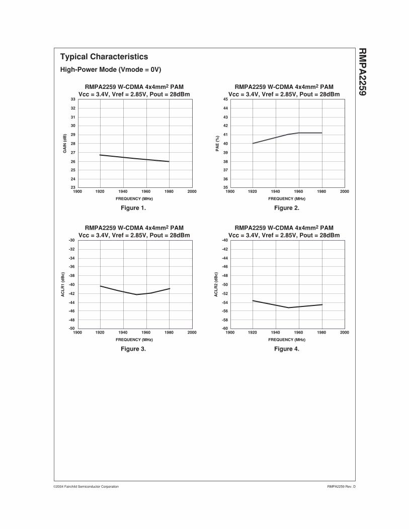
Figure 1.
RMPA2259 W-CDMA 4x4mm2 PAMVcc = 3.4V, Vref = 2.85V, Pout = 28dBm
RMPA2259 W-CDMA 4x4mm2 PAMVcc = 3.4V, Vref = 2.85V, Pout = 28dBm
GA
IN (
dB
)
FREQUENCY (MHz)
23
24
25
26
27
28
29
30
31
32
33
200019801960194019201900
Figure 2.P
AE
(%
)
FREQUENCY (MHz)
35
36
37
38
39
40
41
42
43
44
45
200019801960194019201900
Figure 3.
RMPA2259 W-CDMA 4x4mm2 PAMVcc = 3.4V, Vref = 2.85V, Pout = 28dBm
RMPA2259 W-CDMA 4x4mm2 PAMVcc = 3.4V, Vref = 2.85V, Pout = 28dBm
AC
LR
1 (d
Bc)
FREQUENCY (MHz)
-50
-48
-46
-44
-42
-40
-38
-36
-34
-32
-30
200019801960194019201900
Figure 4.
AC
LR
2 (d
Bc)
FREQUENCY (MHz)
-60
-58
-56
-54
-52
-50
-48
-46
-44
-42
-40
200019801960194019201900
Typical Characteristics
High-Power Mode (Vmode = 0V)
©2004 Fairchild Semiconductor Corporation RMPA2259 Rev. D
RM
PA
2259
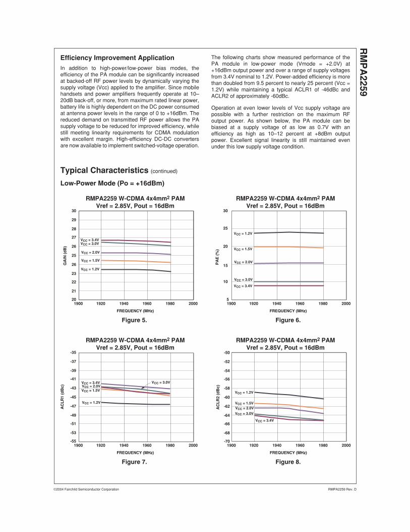
Figure 5.
RMPA2259 W-CDMA 4x4mm2 PAMVref = 2.85V, Pout = 16dBm
RMPA2259 W-CDMA 4x4mm2 PAMVref = 2.85V, Pout = 16dBm
AC
LR
1 (d
Bc)
FREQUENCY (MHz)
VCC = 3.4V
VCC = 3.4V
VCC = 3.0V
VCC = 3.0V
VCC = 2.0V
VCC = 2.0VVCC = 1.5V
VCC = 1.5V
VCC = 1.2V
VCC = 1.2V
20
21
22
23
26
25
26
27
28
29
30
20001980196019401920
FREQUENCY (MHz)
20001980196019401920
1900
1900
FREQUENCY (MHz)
200019801960194019201900
Figure 6.
FREQUENCY (MHz)
5
10
15
20
25
30
200019801960194019201900
-55
-53
-51
-49
-47
-45
-43
-41
-39
-37
-35
Figure 7.
RMPA2259 W-CDMA 4x4mm2 PAMVref = 2.85V, Pout = 16dBm
RMPA2259 W-CDMA 4x4mm2 PAMVref = 2.85V, Pout = 16dBm
GA
IN (
dB
)
Figure 8.
PA
E (
%)
VCC = 3.4V VCC = 3.0V
VCC = 3.0V
VCC = 2.0V
VCC = 3.4V
VCC = 2.0V
VCC = 1.5V
VCC = 1.5VVCC = 1.2V
VCC = 1.2V
AC
LR
2 (d
Bc)
-70
-68
-66
-64
-62
-60
-58
-56
-54
-52
-50
Efficiency Improvement Application
In addition to high-power/low-power bias modes, theefficiency of the PA module can be significantly increasedat backed-off RF power levels by dynamically varying thesupply voltage (Vcc) applied to the amplifier. Since mobilehandsets and power amplifiers frequently operate at 10–20dB back-off, or more, from maximum rated linear power,battery life is highly dependent on the DC power consumedat antenna power levels in the range of 0 to +16dBm. Thereduced demand on transmitted RF power allows the PAsupply voltage to be reduced for improved efficiency, whilestill meeting linearity requirements for CDMA modulationwith excellent margin. High-efficiency DC-DC convertersare now available to implement switched-voltage operation.
The following charts show measured performance of thePA module in low-power mode (Vmode = +2.0V) at+16dBm output power and over a range of supply voltagesfrom 3.4V nominal to 1.2V. Power-added efficiency is morethan doubled from 9.5 percent to nearly 25 percent (Vcc =1.2V) while maintaining a typical ACLR1 of -46dBc andACLR2 of approximately -60dBc.
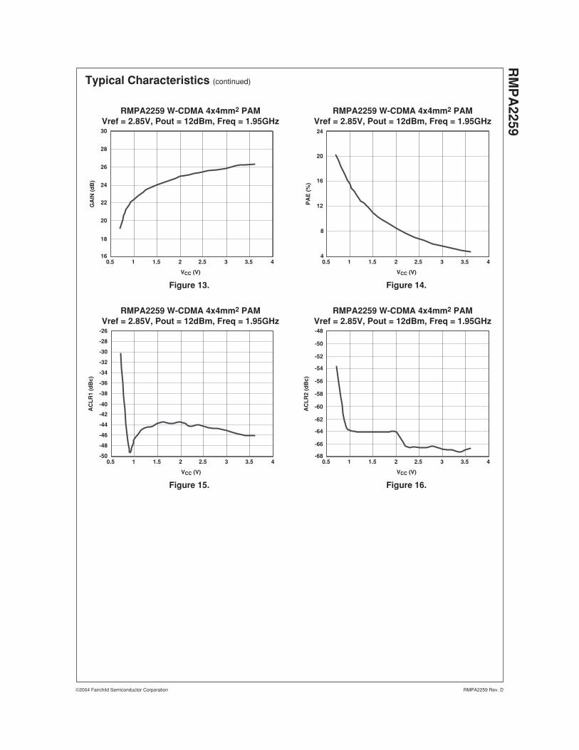
Operation at even lower levels of Vcc supply voltage arepossible with a further restriction on the maximum RFoutput power. As shown below, the PA module can bebiased at a supply voltage of as low as 0.7V with anefficiency as high as 10–12 percent at +8dBm outputpower. Excellent signal linearity is still maintained evenunder this low supply voltage condition.
Typical Characteristics
(continued)
Low-Power Mode (Po = +16dBm)

©2004 Fairchild Semiconductor Corporation RMPA2259 Rev. D
RM
PA
2259
Figure 9.
RMPA2259 W-CDMA 4x4mm2 PAMVref = 2.85V, Pout = 16dBm, Freq = 1.95GHz
RMPA2259 W-CDMA 4x4mm2 PAMVref = 2.85V, Pout = 16dBm, Freq = 1.95GHz
Gai
n (
dB
)
VCC (V)
16
18
20
22
24
26
28
30
42 2.5 3 3.51.510.5
Figure 10.
Figure 11.
RMPA2259 W-CDMA 4x4mm2 PAMVref = 2.85V, Pout = 16dBm, Freq = 1.95GHz
RMPA2259 W-CDMA 4x4mm2 PAMVref = 2.85V, Pout = 16dBm, Freq = 1.95GHz
Figure 12.
PA
E (
%)
VCC (V)
8
12
16
20
24
28
32
42 2.5 3 3.51.510.5
AC
LR
2 (d
Bc)
VCC (V)
-68
-66
-64
-62
-60
-58
-56
-54
-52
-50
-48
42 2.5 3 3.51.510.5
AC
LR
1 (d
Bc)
VCC (V)
-50
-48
-42
-44
-46
-40
-38
-36
-34
-32
-30
-28
-26
42 2.5 3 3.51.510.5
Typical Characteristics
(continued)
©2004 Fairchild Semiconductor Corporation RMPA2259 Rev. D
RM
PA
2259
Figure 13.
RMPA2259 W-CDMA 4x4mm2 PAMVref = 2.85V, Pout = 12dBm, Freq = 1.95GHz
RMPA2259 W-CDMA 4x4mm2 PAMVref = 2.85V, Pout = 12dBm, Freq = 1.95GHz
GA
IN (
dB
)
VCC (V)
16
18
20
22
24
26
28
30
42 2.5 3 3.51.510.5
Figure 14.
Figure 15.
RMPA2259 W-CDMA 4x4mm2 PAMVref = 2.85V, Pout = 12dBm, Freq = 1.95GHz
RMPA2259 W-CDMA 4x4mm2 PAMVref = 2.85V, Pout = 12dBm, Freq = 1.95GHz
Figure 16.
PA
E (
%)
VCC (V)
4
8
12
16
20
24
42 2.5 3 3.51.510.5
AC
LR
2 (d
Bc)
VCC (V)
-68
-66
-64
-62
-60
-58
-56
-54
-52
-50
-48
42 2.5 3 3.51.510.5
AC
LR
1 (d
Bc)
VCC (V)
-50
-48
-42
-44
-46
-40
-38
-36
-34
-32
-30
-28
-26
42 2.5 3 3.51.510.5
Typical Characteristics
(continued)

©2004 Fairchild Semiconductor Corporation RMPA2259 Rev. D
RM
PA
2259
Figure 17.
RMPA2259 W-CDMA 4x4mm2 PAMVref = 2.85V, Pout = 8dBm, Freq = 1.95GHz
RMPA2259 W-CDMA 4x4mm2 PAMVref = 2.85V, Pout = 8dBm, Freq = 1.95GHz
GA
IN (
dB
)
VCC (V)
16
18
20
22
24
26
28
30
42 2.5 3 3.51.510.5
Figure 18.
Figure 19.
RMPA2259 W-CDMA 4x4mm2 PAMVref = 2.85V, Pout = 8dBm, Freq = 1.95GHz
RMPA2259 W-CDMA 4x4mm2 PAMVref = 2.85V, Pout = 8dBm, Freq = 1.95GHz
Figure 20.
0
2
4
6
8
10
12
14
42 2.5 3 3.51.510.5
PA
E (
%)
VCC (V)
AC
LR
2 (d
Bc)
VCC (V)
-68
-70
-66
-64
-62
-60
-58
-56
-54
-52
-50
42 2.5 3 3.51.510.5
AC
LR
1 (d
Bc)
VCC (V)
-53
-55
-51
-49
-47
-45
-43
-41
-39
-37
-35
42 2.5 3 3.51.510.5
Typical Characteristics
(continued)

©2004 Fairchild Semiconductor Corporation RMPA2259 Rev. D
RM
PA
2259
Applications Information
CAUTION: THIS IS AN ESD SENSITIVE DEVICE.
Precautions to Avoid Permanent Device Damage:
• Cleanliness: Observe proper handling procedures toensure clean devices and PCBs. Devices should remainin their original packaging until component placement toensure no contamination or damage to RF, DC andground contact areas.
• Device Cleaning: Standard board cleaning techniquesshould not present device problems provided that theboards are properly dried to remove solvents or waterresidues.
• Static Sensitivity: Follow ESD precautions to protectagainst ESD damage:
– A properly grounded static-dissipative surface onwhich to place devices.
– Static-dissipative floor or mat.
– A properly grounded conductive wrist strap for eachperson to wear while handling devices.
• General Handling: Handle the package on the top with avacuum collet or along the edges with a sharp pair ofbent tweezers. Avoiding damaging the RF, DC, andground contacts on the package bottom. Do not applyexcessive pressure to the top of the lid.
• Device Storage: Devices are supplied in heat-sealed,moisture-barrier bags. In this condition, devices areprotected and require no special storage conditions.Once the sealed bag has been opened, devices shouldbe stored in a dry nitrogen environment.
Device Usage:
Fairchild recommends the following procedures prior toassembly.
• Dry-bake devices at 125°C for 24 hours minimum. Note:The shipping trays cannot withstand 125°C bakingtemperature.
• Assemble the dry-baked devices within 7 days ofremoval from the oven.
• During the 7-day period, the devices must be stored in anenvironment of less than 60% relative humidity and amaximum temperature of 30°C
• If the 7-day period or the environmental conditions havebeen exceeded, then the dry-bake procedure must berepeated.
Solder Materials & Temperature Profile:
Reflow soldering is the preferred method of SMTattachment. Hand soldering is not recommended.
Reflow Profile
• Ramp-up: During this stage the solvents are evaporatedfrom the solder paste. Care should be taken to preventrapid oxidation (or paste slump) and solder burstscaused by violent solvent out-gassing. A typical heatingrate is 1- 2°C/sec.
• Pre-heat/soak: The soak temperature stage serves twopurposes; the flux is activated and the board and devicesachieve a uniform temperature. The recommended soakcondition is: 120–150 seconds at 150°C.
• Reflow Zone: If the temperature is too high, then devicesmay be damaged by mechanical stress due to thermalmismatch or there may be problems due to excessivesolder oxidation. Excessive time at temperature canenhance the formation of inter-metallic compounds atthe lead/board interface and may lead to earlymechanical failure of the joint. Reflow must occur prior tothe flux being completely driven off. The duration of peakreflow temperature should not exceed 10 seconds.Maximum soldering temperatures should be in the range215–220°C, with a maximum limit of 225°C.
• Cooling Zone: Steep thermal gradients may give rise toexcessive thermal shock. However, rapid coolingpromotes a finer grain structure and a more crack-resistant solder joint. The illustration below indicates therecommended soldering profile.
Solder Joint Characteristics:
Proper operation of this device depends on a reliable void-free attachment of the heat sink to the PWB. The solderjoint should be 95% void-free and be a consistentthickness.
Rework Considerations:
Rework of a device attached to a board is limited to reflowof the solder with a heat gun. The device should not besubjected to more than 225°C and reflow solder in themolten state for more than 5 seconds. No more than 2rework operations should be performed.

©2004 Fairchild Semiconductor Corporation RMPA2259 Rev. D
RM
PA
2259
0
20
40
60
80
100
120
140
DEG (°C)
TIME (SEC)
10 SEC
183°C
1°C/SEC 1°C/SECSOAK AT 150°CFOR 60 SEC
45 SEC (MAX)ABOVE 183°C
160
180
200
220
240
0 60 120 180 240 300
210
8
3,6,7,9
SMA1RF IN Vcc2
(PACKAGE BASE)
50 ohm TRL50 ohm TRL
3.3 µF
Vref
RMPA2259PYYWW
3.3 µF 1000 pF1000 pF
1000 pF0.1 µF
4Vmode
115
SMA2RF OUT
Vcc1 1
U31XX
Recommended Solder Reflow Profile
Evaluation Board Schematic

©2004 Fairchild Semiconductor Corporation RMPA2259 Rev. D
RM
PA
2259
365 6
5
75
4
1
2
Evaluation Board Layout
Materials List
DC Turn On Sequence:
1. Vcc1 = Vcc2 = 3.4V (typical)
2. Vref = 2.85V (typical)
3. Vmode = 2.0V (Pout < 16dBm), 0V (Pout > 16dBm)
Qty Item No. Part Number Description Vendor
1 1 G657553-1 V2 PC Board Fairchild
2 2 #142-0701-841 SMA Connector Johnson
3 3 #2340-5211TN Terminals 3M
Ref 4 G65758 4- Assembly, RMPA1959 Fairchild
3 5 GRM39XR102KS0V 1000pF Capacitor (0603) Murata
3 5 (Alt) ECJ-1V81H102K 1000pF Capacitor (0603) Panasonic
2 6 C3216X5R1A335M 3.3µF Capacitor (1206) TDK
1 7 GRM39YSV104Z16V 0.1µF Capacitor (0603) Murate
1 7 (Alt) ECJ-1VB1CID4K 0.1µF Capacitor (0603) Panasonic
A/R 8 SN63 Solder Paste Indium Corp.
A/R 9 SN96 Solder Paste Indium Corp

©2004 Fairchild Semiconductor Corporation RMPA2259 Rev. D
RM
PA
2259
Bottom View
Top ViewFront View
0.1378 (3.50)Typ.
0.1436 (3.65)
0.0098 (0.25)Typ.
0.0425 (1.08)
1
2
3
4
5
10
9
8
7
6
0.0724 (1.84)
Pin 1 Indicator
0.0118 (0.30)Typ.
0.0069 (0.18)
0.0335 (0.85)Typ.
0.1575(4.00 )
+.004– 0.02
+.100–0.00
0.0830 (1.60)
Dimensions are in inches (mm)
2x
PA2259PYYWWU31XX
Package Outline
Package Pinout
Pin # Signal Name Description
1 Vcc1 Supply Voltage to Input Stage
2 RF In RF Input Signal
3 GND Ground
4 Vmode High-Power/Low-Power Mode Control
5 Vref Reference Voltage
6 GND Ground
7 GND Ground
8 RF Out RF Output Signal
9 GND Ground
10 Vcc2 Supply Voltage to Output Stage
11 GND Paddle Ground

DISCLAIMER
FAIRCHILD SEMICONDUCTOR RESERVES THE RIGHT TO MAKE CHANGES WITHOUT FURTHER NOTICE TO ANYPRODUCTS HEREIN TO IMPROVE RELIABILITY, FUNCTION OR DESIGN. FAIRCHILD DOES NOT ASSUME ANY LIABILITYARISING OUT OF THE APPLICATION OR USE OF ANY PRODUCT OR CIRCUIT DESCRIBED HEREIN; NEITHER DOES ITCONVEY ANY LICENSE UNDER ITS PATENT RIGHTS, NOR THE RIGHTS OF OTHERS.
TRADEMARKS
The following are registered and unregistered trademarks Fairchild Semiconductor owns or is authorized to use and isnot intended to be an exhaustive list of all such trademarks.
LIFE SUPPORT POLICY
FAIRCHILD’S PRODUCTS ARE NOT AUTHORIZED FOR USE AS CRITICAL COMPONENTS IN LIFE SUPPORTDEVICES OR SYSTEMS WITHOUT THE EXPRESS WRITTEN APPROVAL OF FAIRCHILD SEMICONDUCTOR CORPORATION.As used herein:1. Life support devices or systems are devices orsystems which, (a) are intended for surgical implant intothe body, or (b) support or sustain life, or (c) whosefailure to perform when properly used in accordancewith instructions for use provided in the labeling, can bereasonably expected to result in significant injury to theuser.
2. A critical component is any component of a lifesupport device or system whose failure to perform canbe reasonably expected to cause the failure of the lifesupport device or system, or to affect its safety oreffectiveness.
PRODUCT STATUS DEFINITIONS
Definition of Terms
Datasheet Identification Product Status Definition
Advance Information
Preliminary
No Identification Needed
Obsolete
This datasheet contains the design specifications forproduct development. Specifications may change inany manner without notice.
This datasheet contains preliminary data, andsupplementary data will be published at a later date.Fairchild Semiconductor reserves the right to makechanges at any time without notice in order to improvedesign.
This datasheet contains final specifications. FairchildSemiconductor reserves the right to make changes atany time without notice in order to improve design.
This datasheet contains specifications on a productthat has been discontinued by Fairchild semiconductor.The datasheet is printed for reference information only.
Formative orIn Design
First Production
Full Production
Not In Production
ISOPLANAR™ LittleFET™
MICROCOUPLER™MicroFET™MicroPak™MICROWIRE™MSX™MSXPro™OCX™OCXPro™OPTOLOGIC
OPTOPLANAR™PACMAN™POP™
FAST
FASTr™ FPS™
FRFET™GlobalOptoisolator™GTO™HiSeC™I2C™i-Lo™ImpliedDisconnect™
Rev. I13
ACEx™ActiveArray™Bottomless™CoolFET™CROSSVOLT™DOME™EcoSPARK™E2CMOS™EnSigna™FACT™FACT Quiet Series™
Power247™PowerEdge™PowerSaver™PowerTrench
QFET
QS™QT Optoelectronics™Quiet Series™RapidConfigure™RapidConnect™µSerDes™SILENT SWITCHER
SMART START™SPM™
Stealth™SuperFET™SuperSOT™-3SuperSOT™-6SuperSOT™-8SyncFET™TinyLogic
TINYOPTO™TruTranslation™UHC™UltraFET
VCX™Across the board. Around the world.™The Power Franchise
Programmable Active Droop™