rocess induced morphology changes during drying of thin ... · tft coating and printing lab at...
TRANSCRIPT

KIT – The cooperation of Forschungszentrum Karlsruhe GmbH and Universität Karlsruhe (TH)
INSTITUTE OF THERMAL PROCESS ENGINEERING – THIN FILM TECHNOLOGY
Process induced morphology changes during drying of thin films for coated and printed electronics
Michael Baunach, K. Peters, B. Schmidt-Hansberg, L. Wengeler, Philip Scharfer, Wilhelm Schabel

TFT – Group
Benjamin Schmidt-Hansberg
WilhelmSchabel
(Shared Professor)
PhilipScharfer
(Head of TFT @ KIT-CN)
JoachimKrenn
YingZhou
LukasWengeler Katharina
Peters
SibylleKachel
Michael Baunach
Philipp Cavadini
Sandra Jeck
(Joint Project)
2 Michael Baunach - UK-German Partnering Workshop: Process technology for
organic and hybrid solar cells.

Thin Film Technology - Research Fields - Examples
3
Organic (Semi-) Conducting Films
Organic Photovoltaic (OPV), Organic LEDs,
Hybrid Solar Cells, Organic Sensors, …
© PHILIPS © Konarka
Source: HOLST CENTER
Fraunhofer ICT
Source: ROCHE
Source: FLEXIBLE DISPLAY CENTER
SOURCE: SZ,
E-Paper
© CEFOTECH
Bioactive Films
Biosensors, Diagnostics, Patches
Biocomps, Medical coatings, …
Foils, Membranes
Optical Films & Foils,
Membranes, Ceramic Foils,
Battery, and Electrode Coatings
Functional Films and Coatings
(Smart-) Coatings, Paints,
Antireflective-, Protective Films, …
Source: ILFORDSource: BAYER
Michael Baunach - Process induced morphology changes during drying of thin
films for coated and printed electronics

TFT coating and printing lab at „KIT-Hightech-Inkubator“
Michael Baunach - Process induced morphology changes during drying of thin
films for coated and printed electronics
4
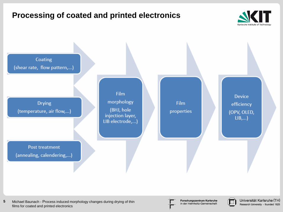
Processing of coated and printed electronics
5 Michael Baunach - Process induced morphology changes during drying of thin
films for coated and printed electronics

Challenges: OPV-Processing and Upscaling
Michael Baunach - Process induced morphology changes during drying of thin
films for coated and printed electronics
6
Sources: 1:(Park et al., 2009), 2: (Dennler, Scharber und Brabec 2009),
3: (Chang et al., 2009), 4: (Kim et al., 2007), 5: (Hoth et al., 2007) ,
6: (Hoth et al., 2009), 7: (Ding et al., 2009),8: (Krebs2, 2009), 9: (Krebs1, 2009).
Coating method Materials Substrate Conditions Electrode R2R PCE Date Ref
Spin Coating PCDTBT/PC70BM Glas Inert ITO NO 6% 2009 1
Spin Coating P3HT/PCBM Glas Inert ITO NO 5% 2009 2
Doctor blade P3HT/PCBM Glas Inert ITO NO >4% 2009 3
Brush painting P3HT/PCBM Glas Inert ITO NO >5% 2007 4
Ink Jet P3HT/PCBM Glas Inert ITO NO 3.5% 2009 5
Spray P3HT/PCBM Glas Inert ITO NO >2,5% 2007 6
Gravure P3HT/PCBM PC Inert ITO NO 1.68% 2009 7
Screen/ Blade /Slot Die P3MHOCT PET Ambient ITO YES 0.84% 2009 8
Slot Die /Screen P3HT/PCBM PEN Ambient ZnOx PDOT YES 0.3% 2009 9
L. Wengeler et al. presented at European Coating Symposium 2009, Karlsruhe
Lab
Pilot
WR for OPV (10/2009): 7.6% PCE
Literature overview
LTI - Lab: ~ 5 % PCE
TFT - Lab (12/2009): 1,6 % PCE

Coating Technology: Pre-metered and Self-metered
Michael Baunach - Process induced morphology changes during drying of thin
films for coated and printed electronics
7
Slot Bead
Slide Curtain
Slot Curtain Source ROTARY COATERSource TSE TROLLER
TFT Lab
TFT Lab
TFT Lab

Roll to Roll (R2R) – coating and drying pilot plant
Roll to Roll:
- Web speed: 0.2 … 20 m/min
- Coating width: 40 … 400 mm
- Dryer length: 2 … 5 m
Michael Baunach - Process induced morphology changes during drying of thin
films for coated and printed electronics
8
Pre-metered
Coating station:
Slot Die/ Slide/ Curtain

Drying channel for defined drying conditions
Raman-Spectroscopy
Gravimetric Measerment
Monochromatic Reflectometry
Michael Baunach - Process induced morphology changes during drying of thin
films for coated and printed electronics
9

100% Solvent
100% Polymer 100% Fullerenez P
olym
er
zFullerene
zSo
lvent
Solubility Limit = f(T)
Solv
ent e
vap
ora
tion
Morphology - drying kinetic – phase separation
Drying kinetics Phase behavior
during drying
Schmidt-Hansberg et al. (2008)
10 Michael Baunach - Process induced morphology changes during drying of thin
films for coated and printed electronics

OPV-Processing: Influence of drying kinetics
11
Fast
Drying
<20 sec
Slow
Drying
>20 min
Drying kinetics
determine solar cell
efficiency!
P3HT:PCBM (1:0.9)
before annealing
B. Schmidt-Hansberg, H. Do, A. Colsmann, U. Lemmer,
W. Schabel, Eur. Phys. J.- ST, 2009, 166, 49-53
G. Li et al., Nature Mater. 4 (2005)
Michael Baunach - Process induced morphology changes during drying of thin
films for coated and printed electronics
In Cooperation with LTI - KIT
(U. Lemmer)
DFG-SPP: JOINT PROPOSAL (Lemmer, Schabel, Ahlswede, Barrena, Höger)

OPV-Processing: Impact of drying conditions on film
topography
Michael Baunach - UK-German Partnering Workshop: Process technology for
organic and hybrid solar cells.
12
AFM scan size 1µm x 1µmGrowing structure size
B. Schmidt-Hansberg, et al., Journal of Applied Physics (accepted)
Same drying time!

OPV-Processing: Simultaneous in situ Reflectometry and
GIXD
13
P3HT Crystal
M. Sanyal, B. Schmidt-Hansberg et al., (submitted)
Monitoring at the same time:
- Drying kinetics (thickness, solvent fraction)
- Crystallization (kinetics of crystallization, orientation, phase transitions)
Michael Baunach - Process induced morphology changes during drying of thin
films for coated and printed electronics

Influence of process steps “coating” and “drying“ on
electrode (anode) morphology
Characterization of electrode: BET, AFM, SEM/TEM, XRD, …
Modelling of process
Michael Baunach - Process induced morphology changes during drying of thin
films for coated and printed electronics
14

Drying experiment with cathode material
Michael Baunach - Process induced morphology changes during drying of thin
films for coated and printed electronics
15
→ Kinetic and thermodynamic properties are dominating the drying process.
Cathode material (IMF III):
LiFePO4 + polymeric binder
+ N-Methyl-2-pyrrolidon (NMP)
In cooperation
W. Bauer (KIT-IMF III)

Michael Baunach - Process induced morphology changes during drying of thin
films for coated and printed electronics
16
Thank you very much for
your attention!
Institute of Thermal Process EngineeringThin Film Technology