rojas, felix and kennel, ralph and cardenas, roberto …eprints.nottingham.ac.uk/37541/1/a new...
TRANSCRIPT
Rojas, Felix and Kennel, Ralph and Cardenas, Roberto and Clare, Jon C. and Diaz, Matias (2016) A new space-vector-modulation algorithm for a three-level four-leg NPC inverter. IEEE Transactions on Energy Conversion, PP (99). pp. 1-13. ISSN 0885-8969
Access from the University of Nottingham repository: http://eprints.nottingham.ac.uk/37541/1/A%20new%20space-vector-modulation%20algorithm%20for%20a%20three-level%20four-leg%20NPC%20inverter.pdf
Copyright and reuse:
The Nottingham ePrints service makes this work by researchers of the University of Nottingham available open access under the following conditions.
This article is made available under the University of Nottingham End User licence and may be reused according to the conditions of the licence. For more details see: http://eprints.nottingham.ac.uk/end_user_agreement.pdf
A note on versions:
The version presented here may differ from the published version or from the version of record. If you wish to cite this item you are advised to consult the publisher’s version. Please see the repository url above for details on accessing the published version and note that access may require a subscription.
For more information, please contact [email protected]
0885-8969 (c) 2016 IEEE. Personal use is permitted, but republication/redistribution requires IEEE permission. See http://www.ieee.org/publications_standards/publications/rights/index.html for more information.
This article has been accepted for publication in a future issue of this journal, but has not been fully edited. Content may change prior to final publication. Citation information: DOI 10.1109/TEC.2016.2605076, IEEETransactions on Energy Conversion
JOURNAL OF LATEX CLASS FILES, VOL. 11, NO. 4, DECEMBER 2012 1
A New Space-Vector-Modulation Algorithm for aThree-Level Four-Leg NPC Inverter
Felix Rojas, Ralph Kennel, IEEE Senior Member, Roberto Cardenas, IEEE Senior Member,Ricardo Repenning, IEEE Member, Jon Clare, IEEE Senior Member, and Matias Diaz, IEEE Student Member
Abstract—For power conversion systems interfaced to 4-wiresupplies, four-leg converters have become a standard solution. Afour-leg converter allows good compensation of zero-sequenceharmonics and full utilization of the dc-link voltage. Theseare very important features when unbalanced and/or non-linearloads are connected to the system. This paper proposes a 3D-SVM algorithm and provides a comprehensive analysis of thealgorithm implemented on a three-level, four-leg NPC converter.The algorithm allows a simple definition of the different switchingpatterns and enables balancing of the dc-link capacitor voltagesusing the redundancies of the converter states. A resonantcontroller is selected as the control strategy to validate theproposed SVM algorithm in a 6kW experimental rig.
Index Terms—Four-Leg Converters, Three level Neutral PointClamped (NPC) inverter, Three Dimensional Space Vector Mod-ulation (3D-SVM).
I. INTRODUCTION
THe Neutral-Point-Clamped (NPC) Voltage-Source In-verter (VSI) is currently the most widely used multilevel
converter topology [1], [2], [3]. Three-level NPC invertershave well known advantages over the conventional two-levelconverter. For instance NPC converters can be connected tomedium voltage systems without requiring a power trans-former [4], they can operate with a relatively high effectiveswitching frequency reducing the total harmonic distortionat the grid/load [5]. Moreover, for a similar application anNPC inverter requires a smaller power filter when comparedwith a conventional two-level VSI [5]. In addition, lower dv/dtvalues, higher efficiency and less stress on the devices are alsoconsidered important advantages of the NPC converter overthe conventional two-level topology [3], [5]. There are severalapplications of the three-level VSI reported in the literature, forinstance in Wind Energy Conversion Systems (WECSs) [4],[6], [7], where the nominal power of single WECs approaches
This work was supported by BMBF Germany Grant Nr. 01DN13018 andFondecyt Chile, Grant Nr. 1140337. The support of the Basal Project FB0008is also acknowledged.
Felix Rojas is with the Electrical Engineering Department, University ofSantiago of Chile, Avenida Ecuador N 3519, Estacion Central, Santiago ([email protected]).
Ralph Kennel is with the Institute for Electrical Drive Systems and PowerElectronics, Technical University of Munich, Arcisstr. 21, 80333, Munich(email [email protected]).
Roberto Cardenas and Matias Diaz are with the Electrical EngineeringDepartment, University of Chile, Avenida Tupper 2007, Santiago, Chile ([email protected], [email protected]).
Jon Clare is with the Department of Electrical and Electronic Engineering,University of Nottingham, Nottingham University Park, Nottingham, NG7,2RD, (email [email protected]).
iaibicif
S2c
S1c
S2b
S1b
S2a
S1a
S1c
S2c
S1b
S2b
S1a
S2a
iP
iC1
C1VC1
VC2C2
iC2
iN
NPio
S1f
S2f
S2f
S1f
abcf
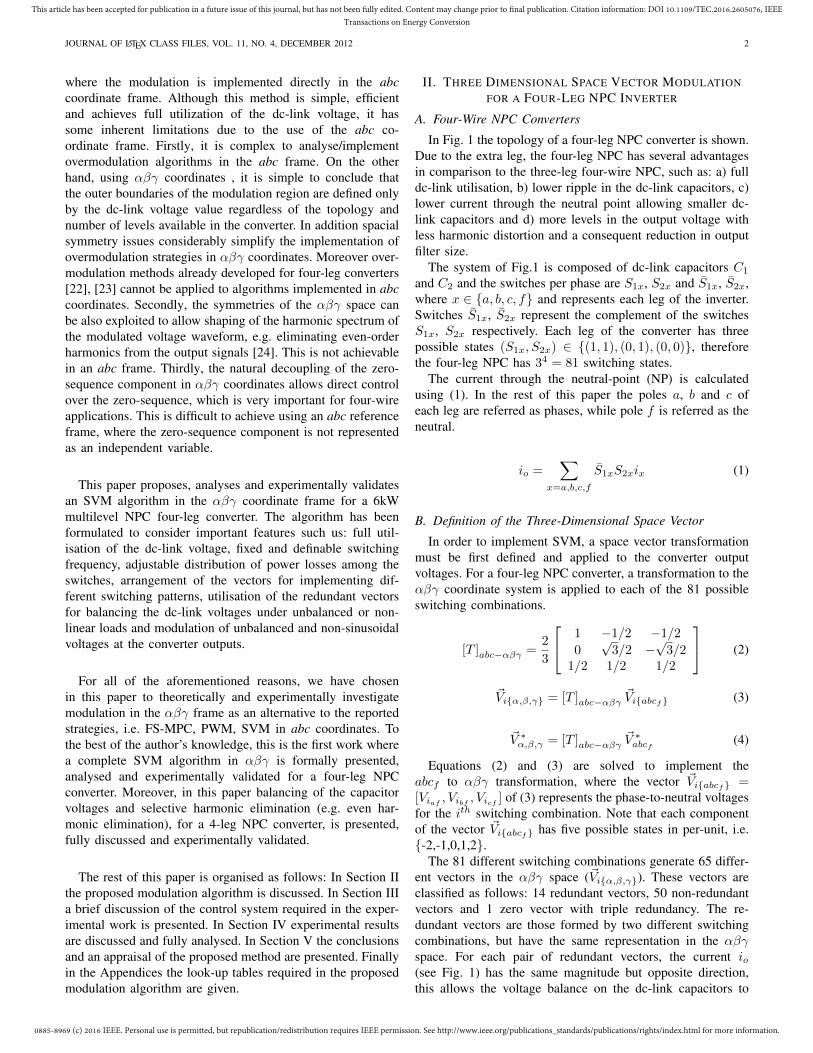
Fig. 1. Electrical diagram for a four-leg Neutral-Point-Clamped Inverter
10MW. In Photovoltaic (PV) applications the three-level NPCis also used because of its good efficiency [1]. Furthermore,applications of the NPC converter as an active filter in mediumvoltage (MV) systems have been also reported [8].
When a path for the circulation of zero-sequence currentsis required, four-leg converters are considered to be one of thesolutions offering most advantages [9],[10]. Several topologiesof 4-leg converters have been discussed in the literature, forinstance applications of the 4-leg, 2-level VSI [11], [12], [9],[13] or 4-leg matrix converter [14], [15] have been extensivelystudied and can be considered relatively mature technologies.4-leg multilevel converters, on the other hand, offer higherefficiency, lower switching losses, higher nominal voltagerange and lower harmonic distortion. However, they have onlybeen proposed recently as an interesting solution for 4-wiresystems, for example in [5], [16], [17] where the applicationof three-level, 4-leg converters is discussed.
Recent research on control systems and modulation algo-rithms for four-leg NPC converters have addressed waveformgeneration and current regulation using non-linear controllerssuch as Finite-Set Model Predictive Control (FS-MPC), totrack output voltage/current references [18], [19]. Unfortu-nately, variability of the switching frequency and the vari-able performance at different operating points are potentialdrawbacks of this approach for grid connected applications.The use of carrier-based Pulse Width Modulation (PWM)applied independently to each leg of the converter has beenaddressed in [20]. However such strategies do not allowselection of variable vector switching sequences to manipulatethe harmonic spectrum or the distribution of the switchingpower losses, which are important in MV or grid connectedapplications. A three dimensional modulation approach for 4-leg three-level NPC converters has been proposed in [21],
0885-8969 (c) 2016 IEEE. Personal use is permitted, but republication/redistribution requires IEEE permission. See http://www.ieee.org/publications_standards/publications/rights/index.html for more information.
This article has been accepted for publication in a future issue of this journal, but has not been fully edited. Content may change prior to final publication. Citation information: DOI 10.1109/TEC.2016.2605076, IEEETransactions on Energy Conversion
JOURNAL OF LATEX CLASS FILES, VOL. 11, NO. 4, DECEMBER 2012 2
where the modulation is implemented directly in the abccoordinate frame. Although this method is simple, efficientand achieves full utilization of the dc-link voltage, it hassome inherent limitations due to the use of the abc co-ordinate frame. Firstly, it is complex to analyse/implementovermodulation algorithms in the abc frame. On the otherhand, using αβγ coordinates , it is simple to conclude thatthe outer boundaries of the modulation region are defined onlyby the dc-link voltage value regardless of the topology andnumber of levels available in the converter. In addition spacialsymmetry issues considerably simplify the implementation ofovermodulation strategies in αβγ coordinates. Moreover over-modulation methods already developed for four-leg converters[22], [23] cannot be applied to algorithms implemented in abccoordinates. Secondly, the symmetries of the αβγ space canbe also exploited to allow shaping of the harmonic spectrum ofthe modulated voltage waveform, e.g. eliminating even-orderharmonics from the output signals [24]. This is not achievablein an abc frame. Thirdly, the natural decoupling of the zero-sequence component in αβγ coordinates allows direct controlover the zero-sequence, which is very important for four-wireapplications. This is difficult to achieve using an abc referenceframe, where the zero-sequence component is not representedas an independent variable.
This paper proposes, analyses and experimentally validatesan SVM algorithm in the αβγ coordinate frame for a 6kWmultilevel NPC four-leg converter. The algorithm has beenformulated to consider important features such us: full util-isation of the dc-link voltage, fixed and definable switchingfrequency, adjustable distribution of power losses among theswitches, arrangement of the vectors for implementing dif-ferent switching patterns, utilisation of the redundant vectorsfor balancing the dc-link voltages under unbalanced or non-linear loads and modulation of unbalanced and non-sinusoidalvoltages at the converter outputs.
For all of the aforementioned reasons, we have chosenin this paper to theoretically and experimentally investigatemodulation in the αβγ frame as an alternative to the reportedstrategies, i.e. FS-MPC, PWM, SVM in abc coordinates. Tothe best of the author’s knowledge, this is the first work wherea complete SVM algorithm in αβγ is formally presented,analysed and experimentally validated for a four-leg NPCconverter. Moreover, in this paper balancing of the capacitorvoltages and selective harmonic elimination (e.g. even har-monic elimination), for a 4-leg NPC converter, is presented,fully discussed and experimentally validated.
The rest of this paper is organised as follows: In Section IIthe proposed modulation algorithm is discussed. In Section IIIa brief discussion of the control system required in the exper-imental work is presented. In Section IV experimental resultsare discussed and fully analysed. In Section V the conclusionsand an appraisal of the proposed method are presented. Finallyin the Appendices the look-up tables required in the proposedmodulation algorithm are given.
II. THREE DIMENSIONAL SPACE VECTOR MODULATIONFOR A FOUR-LEG NPC INVERTER
A. Four-Wire NPC Converters
In Fig. 1 the topology of a four-leg NPC converter is shown.Due to the extra leg, the four-leg NPC has several advantagesin comparison to the three-leg four-wire NPC, such as: a) fulldc-link utilisation, b) lower ripple in the dc-link capacitors, c)lower current through the neutral point allowing smaller dc-link capacitors and d) more levels in the output voltage withless harmonic distortion and a consequent reduction in outputfilter size.
The system of Fig.1 is composed of dc-link capacitors C1
and C2 and the switches per phase are S1x, S2x and S1x, S2x,where x ∈ a, b, c, f and represents each leg of the inverter.Switches S1x, S2x represent the complement of the switchesS1x, S2x respectively. Each leg of the converter has threepossible states (S1x, S2x) ∈ (1, 1), (0, 1), (0, 0), thereforethe four-leg NPC has 34 = 81 switching states.
The current through the neutral-point (NP) is calculatedusing (1). In the rest of this paper the poles a, b and c ofeach leg are referred as phases, while pole f is referred as theneutral.
io =∑
x=a,b,c,f
S1xS2xix (1)
B. Definition of the Three-Dimensional Space Vector
In order to implement SVM, a space vector transformationmust be first defined and applied to the converter outputvoltages. For a four-leg NPC converter, a transformation to theαβγ coordinate system is applied to each of the 81 possibleswitching combinations.
[T ]abc−αβγ =2
3
1 −1/2 −1/2
0√
3/2 −√
3/21/2 1/2 1/2
(2)
~Viα,β,γ = [T ]abc−αβγ~Viabcf (3)
~V ∗α,β,γ = [T ]abc−αβγ~V ∗abcf (4)
Equations (2) and (3) are solved to implement theabcf to αβγ transformation, where the vector ~Viabcf =[Viaf , Vibf , Vicf ] of (3) represents the phase-to-neutral voltagesfor the ith switching combination. Note that each componentof the vector ~Viabcf has five possible states in per-unit, i.e.-2,-1,0,1,2.
The 81 different switching combinations generate 65 differ-ent vectors in the αβγ space (~Viα,β,γ). These vectors areclassified as follows: 14 redundant vectors, 50 non-redundantvectors and 1 zero vector with triple redundancy. The re-dundant vectors are those formed by two different switchingcombinations, but have the same representation in the αβγspace. For each pair of redundant vectors, the current io(see Fig. 1) has the same magnitude but opposite direction,this allows the voltage balance on the dc-link capacitors to
0885-8969 (c) 2016 IEEE. Personal use is permitted, but republication/redistribution requires IEEE permission. See http://www.ieee.org/publications_standards/publications/rights/index.html for more information.
This article has been accepted for publication in a future issue of this journal, but has not been fully edited. Content may change prior to final publication. Citation information: DOI 10.1109/TEC.2016.2605076, IEEETransactions on Energy Conversion
JOURNAL OF LATEX CLASS FILES, VOL. 11, NO. 4, DECEMBER 2012 3
be controlled. Table A.1 in Appendix A, summarizes thisinformation for each vector. Redundant vectors are representedas Vxn or Vxp, for x ∈ [1, 14], where the sub-index n or pdistinguishes the relative polarity of the current io . In additionthe magnitude of each vector is presented in Table A.1 toemphasise that ten different amplitudes are present. Hencethe normal classification of short, medium and long vectors,typically used for the three-leg NPC converter, is no longerapplicable.
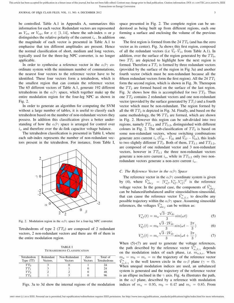
In order to synthesise a reference vector in the αβγ co-ordinate system with the minimum number of commutations,the nearest four vectors to the reference vector have to beidentified. These four vectors form a tetrahedron, which isthe smallest region that can contain the reference vector.The 65 different vectors of Table A.1, generate 192 differenttetrahedrons in the αβγ space, which together make up theentire modulation region for the four-leg NPC as shown inFig. 2.
In order to generate an algorithm for computing the SVMwithout a large number of tables, it is useful to classify eachtetrahedron based on the number of non-redundant vectors theypossess. In addition this classification gives a better under-standing of how the αβγ space is arranged for control overio and therefore over the dc-link capacitor voltage balance.
The tetrahedron classification is presented in Table I, whereeach sub-index represents the number of non-redundant vec-tors present in the tetrahedron. For instance, from Table I,
0
0
0
2
-2
2
-2
-2
2
α
β
γ
Fig. 2. Modulation region in the αβγ space for a four-leg NPC converter.
Tetrahedrons of type 2 (TT2) are composed of 2 redundantvectors, 2 non-redundant vectors and there are 48 of them inthe entire modulation region.
TABLE ITETRAHEDRONS CLASSIFICATION
Tetrahedron Redundant Non-Redundant Zero Total ofType (TT) Vectors. Vectors Vectors TetrahedronsTT0 3 0 1 24TT1 3 1 0 24TT2 2 2 0 48TT3 1 3 0 96
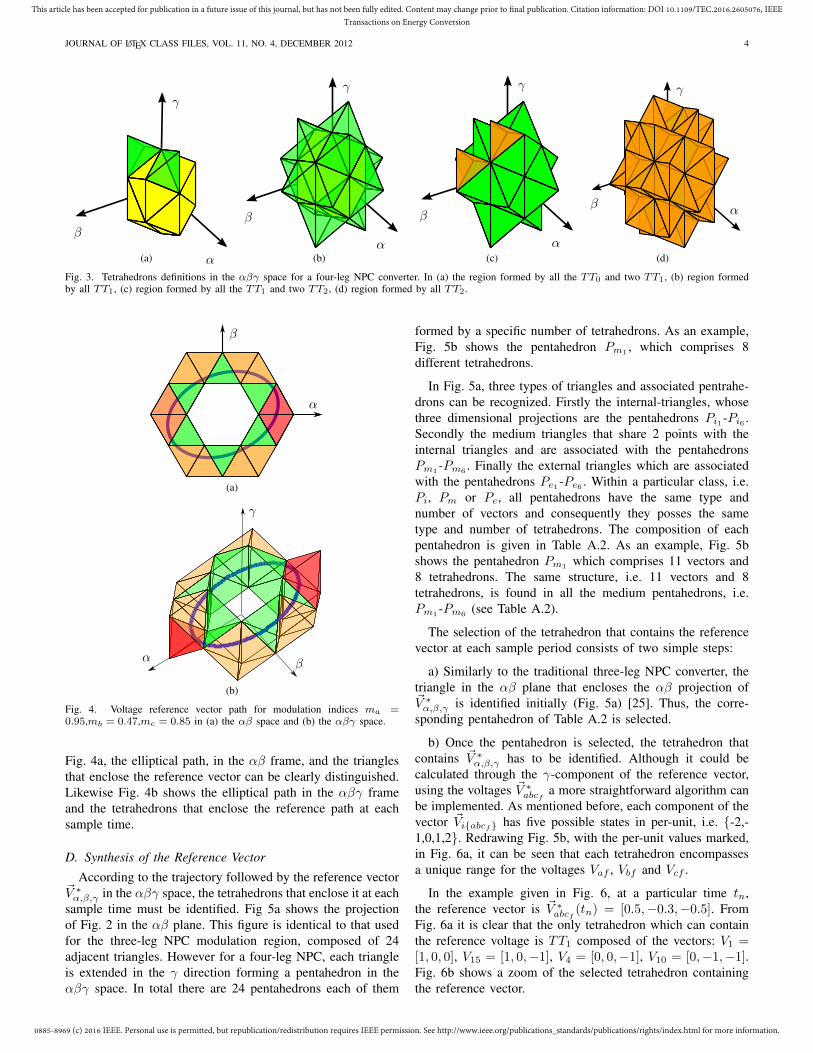
Figs. 3a to 3d show the internal regions of the modulation
space presented in Fig. 2. The complete region can be un-derstood as being built up from different regions, each oneforming a surface and enclosing the volume of the previousone.
The first region is formed from the 24 TT0 (and has the zerovector as its center). Fig. 3a shows this first region, composedof all the redundant vectors (i.e ~V0–~V14 from Table A.1). Inaddition, over the surface of the region generated by the TT0,two TT1 are depicted to highlight how the next region isformed. Therefore a TT1 is formed by three redundant vectors(provided by the surface of the region in Fig 3a) and anotherfourth vector (which must be non-redundant because all thefifteen redundant vectors form the first region). All the 24 TT1
form the second region, which is shown in Fig. 3b. Thereuponthe TT2 are formed based on the surface of the last region.Fig. 3c shows how this is accomplished for two TT2. Thusone TT2 contains 2 redundant vectors and one non-redundantvector (provided by the surface generated by TT1) and a fourthvector which must be non-redundant. The region formed byall the 48 TT2 is depicted in Fig. 3d. Finally, and based on thesame methodology, the 96 TT3 are formed, which are shownin Fig. 2. However this region can be sub-divided into tworegions, namely TT3.1 and TT3.2, distinguished with differentcolours in Fig. 2. The sub-classification of TT3 is based onsome non-redundant vectors, whose switching combinationsgenerate zero current io (~V30− ~V35 and ~V57− ~V64), this leadsto two slightly different TT3. Both of them, TT3.1 and TT3.2,are composed of one redundant vector and 3 non-redundantvectors, however in TT3.1 the three non-redundant vectorsgenerate a non-zero current io, while in TT3.2 only two non-redundant vectors generate a non-zero current io.
C. The Reference Vector in the αβγ Space
The reference vector in the αβγ coordinate system is givenby (4), where ~V ∗abcf = [V ∗af , V
∗bf , V
∗cf ]T is the reference
voltage vector. In the general case, the components of ~V ∗abcfcan be balanced/unbalanced and/or sinusoidal/non-sinusoidal,that can cause the reference vector ~V ∗α,β,γ to describe anypossible trajectory within the αβγ space. Assuming sinusoidalreferences, the voltages ~V ∗abcf can be written as:
V ∗af (t) = ma
√3 · 2Vdc
3sin(ωt) (5)
V ∗bf (t) = mb
√3 · 2Vdc
3sin(ωt− 2π
3) (6)
V ∗cf (t) = mc
√3 · 2Vdc
3sin(ωt+
2π
3) (7)
When (5)-(7) are used to generate the voltage references,the path described by the reference vector ~V ∗α,β,γ dependson the modulation index of each phase, i.e. ma,b,c. Whenma = mb = mc = m the trajectory of the reference vector~V ∗α,β,γ is the well known circle in the α-β plane (γ = 0).When unequal modulation indices are used, an unbalancedsystem is generated and the trajectory of the reference vectoris an ellipse inclined in the γ axis. Fig. 4a illustrates the path,in the αβ plane, described by a reference with modulationindices of ma = 0.95, mb = 0.47 and mc = 0.85. From
0885-8969 (c) 2016 IEEE. Personal use is permitted, but republication/redistribution requires IEEE permission. See http://www.ieee.org/publications_standards/publications/rights/index.html for more information.
This article has been accepted for publication in a future issue of this journal, but has not been fully edited. Content may change prior to final publication. Citation information: DOI 10.1109/TEC.2016.2605076, IEEETransactions on Energy Conversion
JOURNAL OF LATEX CLASS FILES, VOL. 11, NO. 4, DECEMBER 2012 4
α
γ
β
(a)α
γ
β
(b)α
γ
β
(c)
α
γ
β
(d)
Fig. 3. Tetrahedrons definitions in the αβγ space for a four-leg NPC converter. In (a) the region formed by all the TT0 and two TT1, (b) region formedby all TT1, (c) region formed by all the TT1 and two TT2, (d) region formed by all TT2.
α
β
(a)
βα
γ
(b)
Fig. 4. Voltage reference vector path for modulation indices ma =0.95,mb = 0.47,mc = 0.85 in (a) the αβ space and (b) the αβγ space.
Fig. 4a, the elliptical path, in the αβ frame, and the trianglesthat enclose the reference vector can be clearly distinguished.Likewise Fig. 4b shows the elliptical path in the αβγ frameand the tetrahedrons that enclose the reference path at eachsample time.
D. Synthesis of the Reference Vector
According to the trajectory followed by the reference vector~V ∗α,β,γ in the αβγ space, the tetrahedrons that enclose it at eachsample time must be identified. Fig 5a shows the projectionof Fig. 2 in the αβ plane. This figure is identical to that usedfor the three-leg NPC modulation region, composed of 24adjacent triangles. However for a four-leg NPC, each triangleis extended in the γ direction forming a pentahedron in theαβγ space. In total there are 24 pentahedrons each of them
formed by a specific number of tetrahedrons. As an example,Fig. 5b shows the pentahedron Pm1
, which comprises 8different tetrahedrons.
In Fig. 5a, three types of triangles and associated pentrahe-drons can be recognized. Firstly the internal-triangles, whosethree dimensional projections are the pentahedrons Pi1 -Pi6 .Secondly the medium triangles that share 2 points with theinternal triangles and are associated with the pentahedronsPm1
-Pm6. Finally the external triangles which are associated
with the pentahedrons Pe1 -Pe6 . Within a particular class, i.e.Pi, Pm or Pe, all pentahedrons have the same type andnumber of vectors and consequently they posses the sametype and number of tetrahedrons. The composition of eachpentahedron is given in Table A.2. As an example, Fig. 5bshows the pentahedron Pm1
which comprises 11 vectors and8 tetrahedrons. The same structure, i.e. 11 vectors and 8tetrahedrons, is found in all the medium pentahedrons, i.e.Pm1 -Pm6 (see Table A.2).
The selection of the tetrahedron that contains the referencevector at each sample period consists of two simple steps:
a) Similarly to the traditional three-leg NPC converter, thetriangle in the αβ plane that encloses the αβ projection of~V ∗α,β,γ is identified initially (Fig. 5a) [25]. Thus, the corre-sponding pentahedron of Table A.2 is selected.
b) Once the pentahedron is selected, the tetrahedron thatcontains ~V ∗α,β,γ has to be identified. Although it could becalculated through the γ-component of the reference vector,using the voltages ~V ∗abcf a more straightforward algorithm canbe implemented. As mentioned before, each component of thevector ~Viabcf has five possible states in per-unit, i.e. -2,-1,0,1,2. Redrawing Fig. 5b, with the per-unit values marked,in Fig. 6a, it can be seen that each tetrahedron encompassesa unique range for the voltages Vaf , Vbf and Vcf .
In the example given in Fig. 6, at a particular time tn,the reference vector is ~V ∗abcf (tn) = [0.5,−0.3,−0.5]. FromFig. 6a it is clear that the only tetrahedron which can containthe reference voltage is TT1 composed of the vectors: V1 =[1, 0, 0], V15 = [1, 0,−1], V4 = [0, 0,−1], V10 = [0,−1,−1].Fig. 6b shows a zoom of the selected tetrahedron containingthe reference vector.

0885-8969 (c) 2016 IEEE. Personal use is permitted, but republication/redistribution requires IEEE permission. See http://www.ieee.org/publications_standards/publications/rights/index.html for more information.
This article has been accepted for publication in a future issue of this journal, but has not been fully edited. Content may change prior to final publication. Citation information: DOI 10.1109/TEC.2016.2605076, IEEETransactions on Energy Conversion
JOURNAL OF LATEX CLASS FILES, VOL. 11, NO. 4, DECEMBER 2012 5
~V51
~V54
~V36
~V4
~V7
~V27~V39
~V15
~V1
~V10~V45
Pm1
Pi3Pe6 Pi1 Pe1
Pm6Pi5Pm4
Pi4Pe7 Pi6 Pe12
Pe11Pm5Pe8
Pe2Pm2Pe5
Pm1Pi2Pm3
Pe4 Pe3
Pe9 Pe10
0 2/3 4/3
0
√3/3
2√
3/3
(a) (b)
Fig. 5. Projection of the full modulation region in the α-β plane (a) andpentahedron Pm1 is the projection in the α-β-γ space of the triangle in theα-β plane (b).
~Vref
~V15
~V1
~V10
~V4
[2,2,1]
[-1,-2,-2]
[-1,-1,-2]
[0,0,-1]
[1,1,0]
[2,1,1][2,1,0]
[1,0,-1][1,0,0]
[0,-1,-1][0,-1,-2]
~Vref
(a) (b)
Fig. 6. In (a) the pentahedron Pm1 with a reference vector is shown, the volt-ages ~Viabcf replace the vector ~V ∗α,β,γ to allow tetrahedron identification.In (b) a close view of the selected tetrahedron is depicted.
E. Duty Cycle Calculation
Once the 4 vectors that define the selected tetrahedronhave been identified, the duty cycle for each vector must becalculated. Mathematically this can be written as:d1d2
d3
=
Va–dα Vb–dα Vc–dαVa–dβ Vb–dβ Vc–dβVa–dγ Vb–dγ Vc–dγ
−1 V ∗α–dV ∗β–dV ∗γ–d
(8)
d4 = 1− d1 − d2 − d3 (9)
Adopting ~Va, ~Vb, ~Vc, ~Vd as the vectors that enclose thereference ~V ∗αβγ , (8) - (9) show the duty cycle calculation(based on the sample period Ts) for each vector. To simplifythe calculation, all vectors are expressed with respect to adisplaced origin located at the end of the fourth vector ~Vd,where ~Vi–d = ~Vi− ~Vd; i = a, b, c, ref. For the experimentalimplementation of (8), the inverse of the matrix has beencalculated using the cofactor method. The equations for thecofactors and the determinant of the matrix shown in (8)are derived off-line and then programmed in the experimentalsystem used in this work (see section IV). Therefore the terms,numerator and denominator, required for the calculation ofeach duty cycle di are calculated on-line and then divided.Calculation of the entire modulation algorithm and the asso-ciate control system occupies only 30µs of processing time inthe control platform presented in Section IV.
F. Switching Sequence Definition
The selection of the switching sequence in an SVM algo-rithm is always a trade-off between the number of commuta-tions, i.e. power losses, and the total harmonic distortion ofthe modulated waveform. In a typical two level inverter, eitherthree or four leg, zero vectors are always used in each sampleperiod along with the active vectors to create the reference vec-tor. Hence, two important categories of modulation sequencescan be differentiated, which mainly differ in the number ofzero-vector redundancies used in the modulation [26], [27].However in an NPC converter, either three or four leg, zero-vectors are not always present in each sample period. Hencethe normal classification is no longer valid. In this paper twopatterns are defined for the NPC SVM. The first one employsall possible redundancies, while the second pattern uses onlyone redundant vector in each sample period. In addition, onlyone switching state change is allowed during the transitionfrom one vector to another. A symmetric PWM pattern is usedin this work.
1) Full-Redundancy Utilisation: Four types of tetrahedronshave been defined, namely TT0, TT1, TT2 and TT3, eachof which possess a different number of redundant vectors.Therefore the use of all redundancies entails a differentnumber of commutations in each type of tetrahedron. Fig.7a shows the switching commutation sequence for each legof the converter and the phase-to-neutral voltages using allthe possible redundancies of the TT1 shown in Fig. 6b.Likewise Fig. 7b shows the switching commutation sequencefor the TT2 formed by ~V15, ~V4, ~V10, ~V45. As this tetrahedronpossesses two redundant vectors instead of the three present inthe previous example, an extra switching commutation in legf is evident, which implies a different switching frequency ineach leg of the converter.
In order to determine a suitable switching sequence usingonly the first column of Table A.1 and Table A.2, a simplealgorithm is implemented. Table II shows the selected vectorsfor each of the above mentioned tetrahedrons. The vectorsare arranged in decreasing amplitude with respect to the γ-component as defined in Table A.1 and are separated accordingto negative and positive redundancy (as non-redundant vectorspossess only one switching combination, they use the entirerow). The pivot vector of the sequence must be the vectorthat possesses the largest number of Positive(P)/Negative(N)states (marked as •). Then starting from this point a descend-ing/ascending direction must be followed until each vectorhas been transitioned once. The arrows of Table II show thesequence for each tetrahedron. This sequence is then mirroredas depicted in Fig. 7.
2) Single-Redundancy Utilisation: Although the previousswitching sequence generates low THD and gives good con-trollability for balancing of the dc-link capacitor voltage, itemploys a high switching frequency and a different switchingfrequency for each leg of the converter, which in somecases may be unacceptable. In order to reduce the switchingfrequency, a method employing single redundancy has beendeveloped. At least one redundancy must be used, becauseit allows control over the dc-link voltage balance, and the
0885-8969 (c) 2016 IEEE. Personal use is permitted, but republication/redistribution requires IEEE permission. See http://www.ieee.org/publications_standards/publications/rights/index.html for more information.
This article has been accepted for publication in a future issue of this journal, but has not been fully edited. Content may change prior to final publication. Citation information: DOI 10.1109/TEC.2016.2605076, IEEETransactions on Energy Conversion
JOURNAL OF LATEX CLASS FILES, VOL. 11, NO. 4, DECEMBER 2012 6
d34d44d14d22
Ts2
Ts
d34d44
d12
d44d34d22
d14d44d34
0
1
-1
0
1
-1
0
1
-1
0
1
-1
1
00
-10
-1
SLa
SLb
SLc
SLf
Vaf
Vbf
Vcf
SLa
SLb
SLc
SLf
Vaf
Vbf
Vcf
SLa
SLb
SLc
SLf
Vaf
Vbf
Vcf
d34
d24d12d42d34
d22
d34d42d12
d24d34
~V4p~V10p~V1p~V15~V4n~V10n~V1n
.Sequence A Mirror Sequence A⇔ Sequence A2 Mirror Sequence A2⇔ Sequence B Mirror Sequence B⇔
d44
d12
d22d32
d42
d32
d22
d12
d44
(a) (b) (c)Fig. 7. Switching commutation for each leg of the four-leg NP converter and the phase-to-neutral output voltages for: (a) full-redundancies sequence fora TT1 formed by ~V1, ~V15, ~V4, ~V10, which sequence is: ~V1n–~V10n–~V4n–~V15–~V1p–~V10p–~V4p ⇔ Mirror, (b) full-redundancies sequence for a TT2formed by ~V15, ~V4, ~V10, ~V45, which sequence is: ~V10n–~V4n–~V15–~V45–~V10p–~V4p ⇔Mirror and (c) one-redundancy sequence for the same TT1 of(a), using ~V10p as pivot, where the sequence is: ~V10p–~V1p–~V15–~V4n–~V10n ⇔Mirror.
redundancy with the largest duty cycle is selected at eachsample time. The sequence pattern is based on the samealgorithm as explained above. However the algorithm stopsonce it reaches the pivot vector redundancy. Thus for examplein the TT1 and using ~V4n as the pivot, the correct sequenceis: ”~V4n–~V15–~V1p–~V10p–~V4p ⇔ Mirror”. Using ~V10p as thepivot, then the sequence is: ”~V10p–~V1p–~V15–~V4n–~V10n ⇔Mirror”. This last sequence is shown in Fig. 7c, whereonly one switching commutation per sample time in eachleg is ensured. Furthermore, by always using the same typeof redundancy (positive or negative) as the pivot, an extraswitching commutation when moving from one tetrahedron toanother is avoided. This sequence pattern yields a switchingfrequency equal to half the sampling frequency for each switchof the converter. This is true also for the fourth leg whichhas to modulate a signal with a frequency of three timesthe fundamental frequency to achieve sinusoidal voltages atthe converter output. In some applications, it is desirableto alternate the type of redundancy every 60 degrees, thiseliminates even harmonics which are very undesirable in gridconnected applications. This is achieved with a negligibleincrement of the switching frequency.
G. Capacitor Voltage Balance
Different techniques to balance the voltages on the dc-link capacitors have been reported in the literature for theconventional three-level, three-leg NPC converter. These areusually categorised as active control, passive control and hys-teresis control. [28], [29], [30]. In this work an active controlmethodology, embedded into the utilisation and selection ofthe SVM redundant vectors, is proposed to balance the ca-pacitor voltages. According to this, a Pulse Width Modulationtechnique is applied, at each sample time, to the redundant
TABLE IISWITCHING SEQUENCE PATTERN.
Full-redundancies sequence
for a TT1• ~V1n ~V1p
[ONNN ] [POOO]
~V15
[PONO]
~V4n • ~V4p[OONO] [PPOP ]
~V10n ~V10p
[ONNO] [POOP ]
Full-redundancies sequence
for a TT2~V15
[PONO]
~V4n • ~V4p[OONO] [PPOP ]
• ~V10n ~V10p
[ONNO] [POOP ]
~V45
[PONP ]
vectors in order to modulate the neutral point current io totrack a reference current (i∗o) and balance the voltages on thedc-link capacitors VC1
and VC2. The reference current i∗o is
provided by an external controller, which is presented in thenext section. Adopting ~Va, ~Vb, ~Vc, ~Vd as the four vectors thatform a specific tetrahedron, the averaged NP current in onesample period can be mathematically expressed as:
i∗o =λa · d1 · ioa(~Va) + λb · d2 · iob(~Vb)+ (10)
λc · d3 · ioc(~Vc) + λd · d4 · iod(~Vd)
dkp = (1 + λi) · dk2
dkn = (1− λi) · dk2
|λi| ≤ 1
i ∈ a, b, c, dk ∈ 1, 2, 3, 4 (11)
where ioi(~Vi) represent the currents through the NP generatedfor each vector and are determined using (1), di are the
0885-8969 (c) 2016 IEEE. Personal use is permitted, but republication/redistribution requires IEEE permission. See http://www.ieee.org/publications_standards/publications/rights/index.html for more information.
This article has been accepted for publication in a future issue of this journal, but has not been fully edited. Content may change prior to final publication. Citation information: DOI 10.1109/TEC.2016.2605076, IEEETransactions on Energy Conversion
JOURNAL OF LATEX CLASS FILES, VOL. 11, NO. 4, DECEMBER 2012 7
Interrupt Acknowledge
ia, ib, ic, VC1and VC2
Measurement of:
Triangle identification in the
Selection of one pentahedronα-β plane.
from Table A.2
Tetrahedron identification
using ~V ∗abcf
Calculation of the duty cycles:
d1, d2, d3 and d4using (8) and (9)
Calculate the sub-duty cycles
using (10) and (11).
New IA?
Definition of the desirable
switching pattern.
Calculation of
i∗o from external
Send IGBT signals
controller (Fig. 9)
i∗o
Fig. 8. Flowchart of 3D-SVM for a four-leg NPC converter.
duty cycles calculated in (8)-(9) and λi represents the sub-modulation indices, which are calculated in order to obtainan average current equal to i∗o. Each redundant vector al-lows modulation of the current generated through the NP byadjusting the duty cycles of each redundancy (positive andnegative), this allows the sub-modulation index λi ∈ [−1, 1].As (10) is a general representation, the sub-modulation indexλi must be set to 1 for non-redundant vectors. Additionally,each current ioi(~Vi) must be calculated from (1) or obtainedfrom a Look-Up Table (LUT) stored in the third column ofTable A.1. Equation (11) shows the calculation of the sub-dutycycles for the redundant vectors, where dkp and dkn representthe sub-duty cycle for the positive and negative redundancyof the redundant vector. The number of indices λi and sub-duty cycle calculations is equal to the number of redundantvectors present in the selected tetrahedron. When the switchingsequence: Single-Redundancy Utilisation of section II is used,only one sub-duty cycle needs to be calculated at each sampletime. Finally, the diagram of Fig. 8 shows the required stepsto implement the proposed SVM algorithm for a four-leg NPCconverter with capacitor voltage balancing.
Calculation Converter
af
ZbZa
Zc
C1
C2
VC1
VC2
A B
C
F4 4
~V ∗ABCF
~VABCF
Linear Load
NPC Four Leg Converter
Lf
Cf
Lσf
a
b
cC
A
F
LC Filter
io
Rfohc (z)(z−1) (Λ)
Pf (s)ZOH(SVM)
PI(z)Pc(s)
~V ∗abcf
i∗o(z)
PlantSampler(Ts)
Pf (z)
ZOH(SVM) Plant
Sampler(Ts)
Calculation(z−1)
i∗o(z)
∆V ∗(z)
∆V (z)
∆V (z)
Pc(z)
B
(a)
(b)
(c)
Fig. 9. Control scheme for the regulation of the output voltage and balanceon the dc-link capacitor for a four-leg NPC converter.
III. PROPOSED RESONANT VOLTAGE CONTROLLER
To experimentally validate the proposed modulationscheme, a prototype converter was constructed and used tofeed an unbalanced three-phase load connected through an LCfilter as shown in Fig. 9a. An additional optional inductanceLσ is considered in the fourth leg. The linear unbalanced loadis composed of impedances Za, Zb and Zc. .
It is well-known that conventional PI controllers are notparticularly suited to regulate sinusoidal signals [10] [31] [32].On the other hand, and according to the internal model prin-ciple [10], resonant controllers can regulate, with zero steadystate error, sinusoidal voltages and currents [32]. Therefore,to control the output voltages of the 4-leg NPC converter, theutilisation of resonant controllers is proposed in this work.
Fig. 9b presents the proposed control systems for regulationof the converter output voltage. In this diagram the converteris represented as a constant gain Λ, the modulation algorithmand the computational delay are represented by a unit delay(z−1) cascaded with a Zero Order Hold (ZOH). The worstcase situation (from the control design viewpoint) is whenthe converter output is unloaded and the plant Pf (s) is solelyrepresented by the lightly-damped LC output power filter. Tosimplify the analysis in the frequency domain, the controlsystem is designed in the s-domain considering the transferfunction of a resonant controller with delay compensation (see[33],[31]).
Rc(s) =k∑
n=1
Rcn(s) =k∑
n=1
Kns cosϑn − ωn sinϑn
s2 + ω2n
(12)
where ωn represents the nth controlled frequency. The angleϑn represents the phase shift between the voltage modulated
0885-8969 (c) 2016 IEEE. Personal use is permitted, but republication/redistribution requires IEEE permission. See http://www.ieee.org/publications_standards/publications/rights/index.html for more information.
This article has been accepted for publication in a future issue of this journal, but has not been fully edited. Content may change prior to final publication. Citation information: DOI 10.1109/TEC.2016.2605076, IEEETransactions on Energy Conversion
JOURNAL OF LATEX CLASS FILES, VOL. 11, NO. 4, DECEMBER 2012 8
by the converter and the voltage regulated at the output. Noticethat ϑn is a function of the frequency ωn and considers thephase shifts introduced by the proposed SVM (one sampleperiod delay), the phase shift introduced by the plant Pf (s)transfer function, etc.
Notice that compensation of the system phase shift angleϑn, in (12) is one of the methods used to compensate the phasemargin of the open loop transfer function G(s) = Rc(s)Pf (s)without using additional lead-lag networks (see [33],[31]).
The plant transfer function Pf (s), considering only thesecond order LC output power filter, is obtained as:
Pf (s) =Vabcf (s)
VABCF (s)=
1
LfCfs2 +RfCfs+ 1(13)
where Lf and Rf represent the inductance with its intrinsicresistance and Cf is the filter capacitance. Using Fig. 9b,and the plant of (13), the controller gain (Kn in (12)) canbe designed. To discretise the s-plane controller of (12),maintaining most of its original performance, the First OrderHold (FOH) discretisation method is used (see [31]).
Using the Nyquist plot, the discrete time performance of theresonant controller can be analysed using the diagram depictedin Fig. 10. From this figure, it is observed that the plot doesnot encircle the point (−1, 0j) ensuring a stable operation. Itsstability margin is usually defined by the minimum distancefrom the plot of G(s) to the point (−1, 0j) [32] (see ηin Fig. 10), which in this design is set to 0.51 (see [32]).Besides analysing the stability and dynamic performance ofthe proposed control system, the Nyquist plot of Fig. 10 couldalso be used for fine adjustment of the controller parameters(see (12)), for instance the gain Kn.
0 0.2-0.2-0.4-1.0 -0.6-0.8
-0.6j
0j
0.6j
σa
σb
σc
z≈ejTsωnat
z ≈ ejTsω+1
z=ejTsωnyq
P zohf (z)Rfohc (z)
η≈0.51
(−1, 0j)
z ≈ ejTsω−1
k0
Fig. 10. Nyquist diagram for design of the resonant controller Rfohc (z).For Rfohc (z): ω1=10 0π rad s−1, K1=70, D1=1.54. For P zohf (z):Lf=1 mH, Cf=67 µF, Rf=0.1 Ω. Ts=1/6000 s, ωnyq=600 0π rad s−1,ωnat=3863 rad s−1.
In order to balance the dc-link capacitor voltages, the refer-ence current i∗o(z) is obtained at the output of a PI controllerand used to calculate the sub-duty cycles of (11). Accordingly,Fig. 9c shows the proposed control scheme to regulate the dc-link capacitor voltages. Considering C1 ≈ C2, the discrete
form of the plant Pc(s), which relates the difference of thevoltages VC1 and VC2 to the current io, is given by:
Pc(z) =VC1(z)− VC2(z)
io(z)=
∆V (z)
io(z)=
TsC(z − 1)
(14)
using (14) the design of the PI controller utilising linearcontrol design methods (e.g. root locus) is simple to achieve.
IV. EXPERIMENTAL VALIDATION
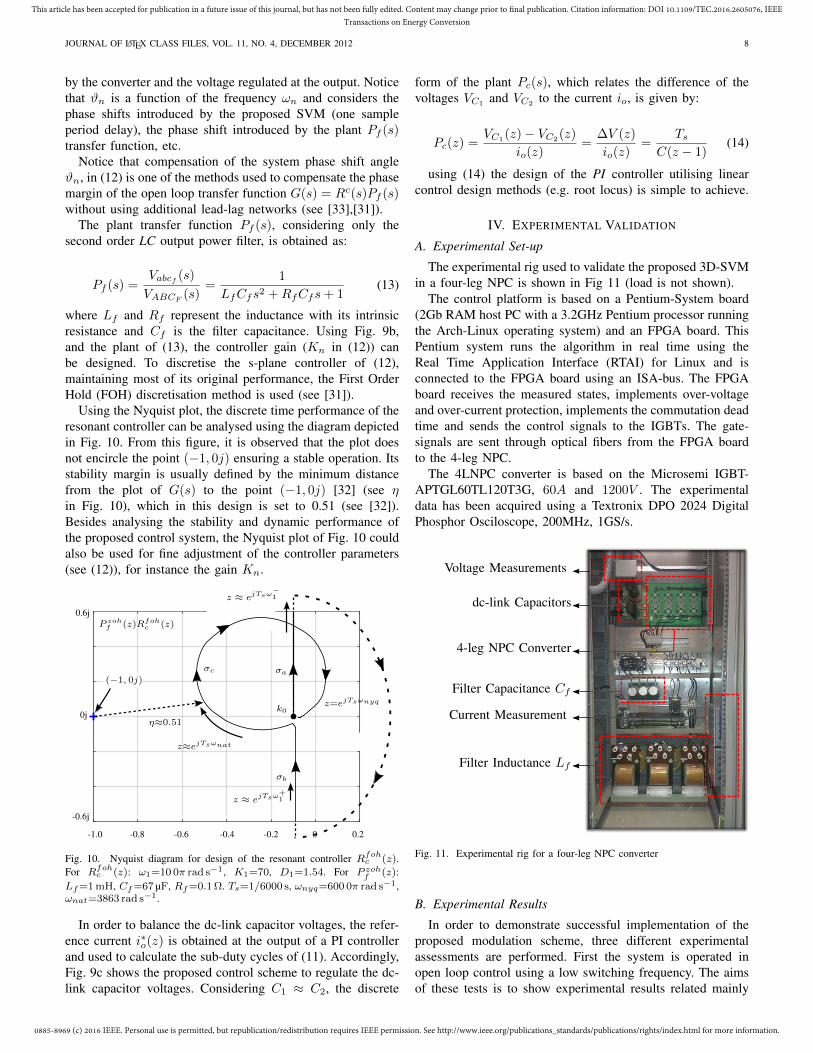
A. Experimental Set-up
The experimental rig used to validate the proposed 3D-SVMin a four-leg NPC is shown in Fig 11 (load is not shown).
The control platform is based on a Pentium-System board(2Gb RAM host PC with a 3.2GHz Pentium processor runningthe Arch-Linux operating system) and an FPGA board. ThisPentium system runs the algorithm in real time using theReal Time Application Interface (RTAI) for Linux and isconnected to the FPGA board using an ISA-bus. The FPGAboard receives the measured states, implements over-voltageand over-current protection, implements the commutation deadtime and sends the control signals to the IGBTs. The gate-signals are sent through optical fibers from the FPGA boardto the 4-leg NPC.
The 4LNPC converter is based on the Microsemi IGBT-APTGL60TL120T3G, 60A and 1200V . The experimentaldata has been acquired using a Textronix DPO 2024 DigitalPhosphor Osciloscope, 200MHz, 1GS/s.
4-leg NPC Converter
Current Measurement
Voltage Measurements
dc-link Capacitors
Filter Inductance Lf
Filter Capacitance Cf
Fig. 11. Experimental rig for a four-leg NPC converter
B. Experimental Results
In order to demonstrate successful implementation of theproposed modulation scheme, three different experimentalassessments are performed. First the system is operated inopen loop control using a low switching frequency. The aimsof these tests is to show experimental results related mainly
0885-8969 (c) 2016 IEEE. Personal use is permitted, but republication/redistribution requires IEEE permission. See http://www.ieee.org/publications_standards/publications/rights/index.html for more information.
This article has been accepted for publication in a future issue of this journal, but has not been fully edited. Content may change prior to final publication. Citation information: DOI 10.1109/TEC.2016.2605076, IEEETransactions on Energy Conversion
JOURNAL OF LATEX CLASS FILES, VOL. 11, NO. 4, DECEMBER 2012 9
to the performance of the modulation algorithm with andwithout considering even harmonic elimination. Secondly thecontrol scheme of Fig. 9 is implemented and experimentallytested considering the proposed SVM algorithm operating withbalanced and unbalanced loads.
Table III shows the parameters used in the experimental im-plementation (Notice that Vdc = VC1 +VC2). All experimentaltests have been performed with the Single − Redundancypattern, discussed in section II.
TABLE IIIGENERAL PARAMETERS OF THE IMPLEMENTED SYSTEMS
Parameter Value Parameter ValueC1 3300 uF Za1 52 Ω ; 10mHC2 3300 uF Zb1 52 Ω ; 10mHVdc 545 V Zc1 52 Ω ; 10mHCf 67 uF Za2 75 Ω ; 10mHLf 1 mH Zb2 52 Ω ; 10mHLσ 0.1 mH Zc2 85 Ω ; 10mH
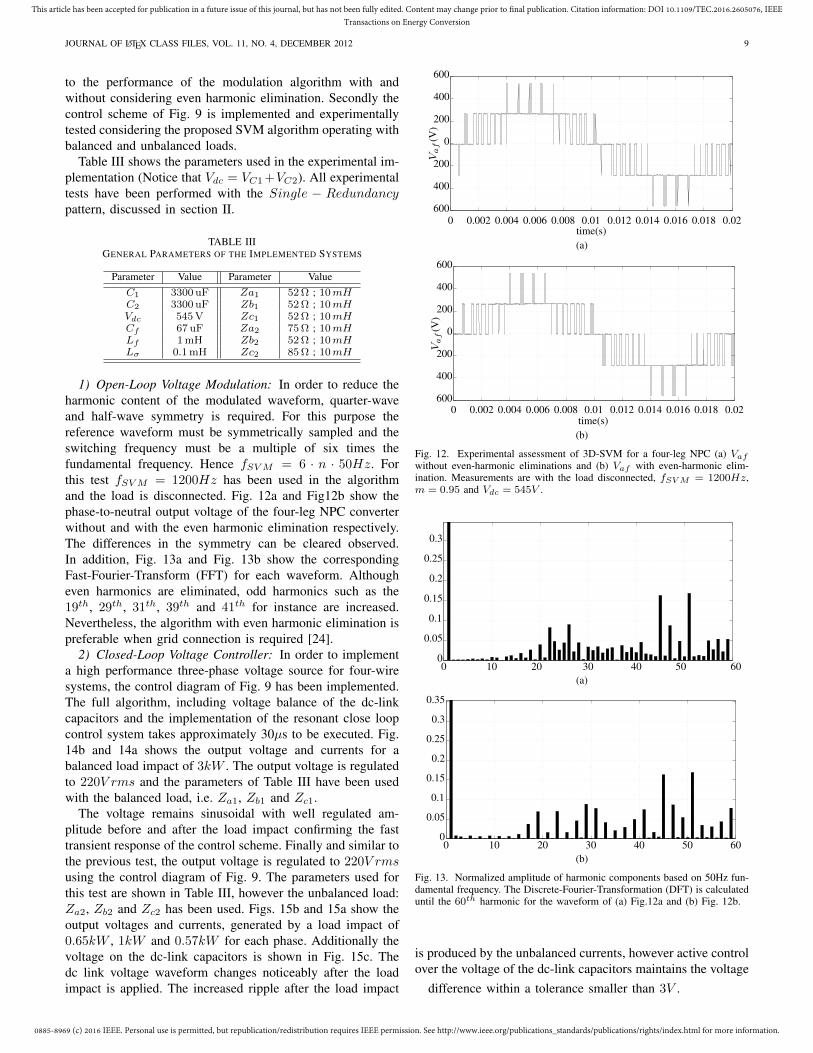
1) Open-Loop Voltage Modulation: In order to reduce theharmonic content of the modulated waveform, quarter-waveand half-wave symmetry is required. For this purpose thereference waveform must be symmetrically sampled and theswitching frequency must be a multiple of six times thefundamental frequency. Hence fSVM = 6 · n · 50Hz. Forthis test fSVM = 1200Hz has been used in the algorithmand the load is disconnected. Fig. 12a and Fig12b show thephase-to-neutral output voltage of the four-leg NPC converterwithout and with the even harmonic elimination respectively.The differences in the symmetry can be cleared observed.In addition, Fig. 13a and Fig. 13b show the correspondingFast-Fourier-Transform (FFT) for each waveform. Althougheven harmonics are eliminated, odd harmonics such as the19th, 29th, 31th, 39th and 41th for instance are increased.Nevertheless, the algorithm with even harmonic elimination ispreferable when grid connection is required [24].
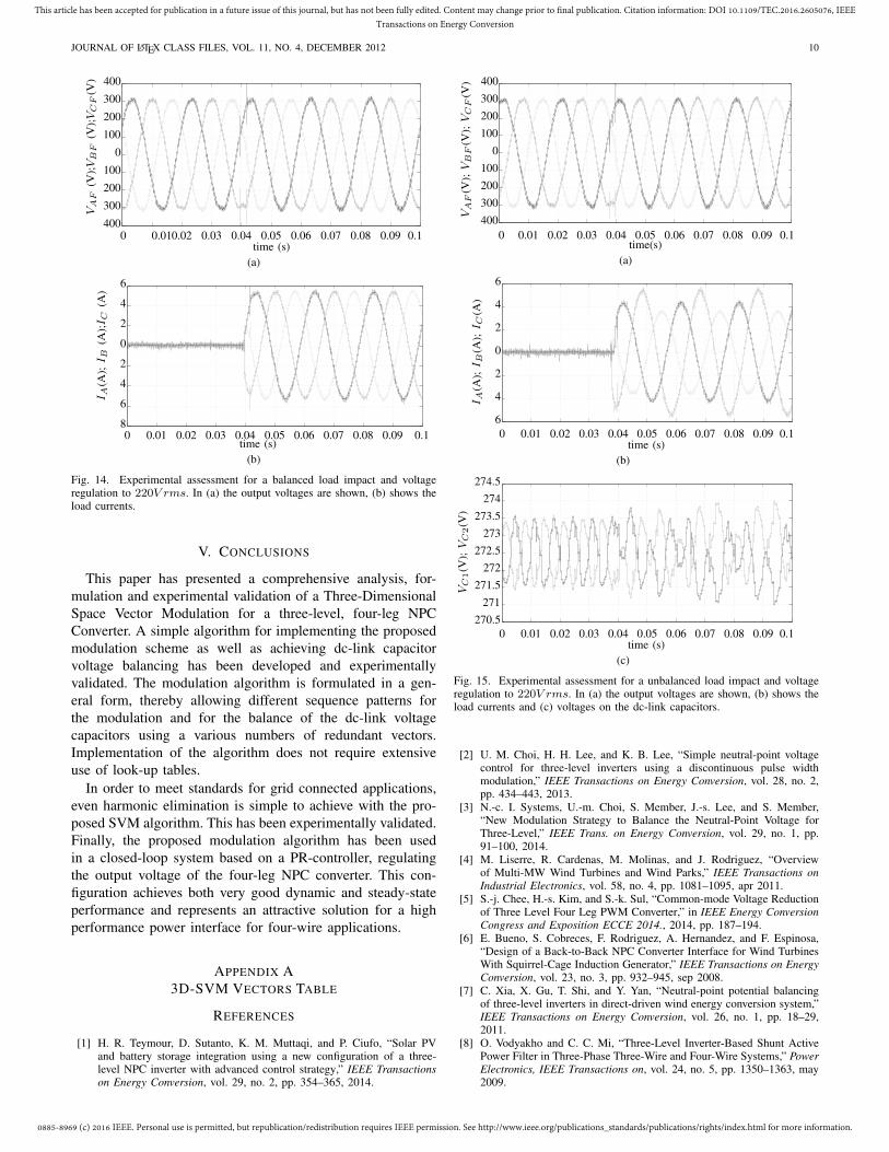
2) Closed-Loop Voltage Controller: In order to implementa high performance three-phase voltage source for four-wiresystems, the control diagram of Fig. 9 has been implemented.The full algorithm, including voltage balance of the dc-linkcapacitors and the implementation of the resonant close loopcontrol system takes approximately 30µs to be executed. Fig.14b and 14a shows the output voltage and currents for abalanced load impact of 3kW . The output voltage is regulatedto 220V rms and the parameters of Table III have been usedwith the balanced load, i.e. Za1, Zb1 and Zc1.
The voltage remains sinusoidal with well regulated am-plitude before and after the load impact confirming the fasttransient response of the control scheme. Finally and similar tothe previous test, the output voltage is regulated to 220V rmsusing the control diagram of Fig. 9. The parameters used forthis test are shown in Table III, however the unbalanced load:Za2, Zb2 and Zc2 has been used. Figs. 15b and 15a show theoutput voltages and currents, generated by a load impact of0.65kW , 1kW and 0.57kW for each phase. Additionally thevoltage on the dc-link capacitors is shown in Fig. 15c. Thedc link voltage waveform changes noticeably after the loadimpact is applied. The increased ripple after the load impact
0 0.002 0.004 0.006 0.008 0.01 0.012 0.014 0.016 0.018 0.02600
400
200
0
200
400
600
time(s)
Vaf
(V)
(a)
0 0.002 0.004 0.006 0.008 0.01 0.012 0.014 0.016 0.018 0.02600
400
200
0
200
400
600
time(s)Vaf
(V)
(b)
Fig. 12. Experimental assessment of 3D-SVM for a four-leg NPC (a) Vafwithout even-harmonic eliminations and (b) Vaf with even-harmonic elim-ination. Measurements are with the load disconnected, fSVM = 1200Hz,m = 0.95 and Vdc = 545V .
0 10 20 30 40 50 600
0.05
0.1
0.15
0.2
0.25
0.3
(a)
0 10 20 30 40 50 600
0.05
0.1
0.15
0.2
0.25
0.3
0.35
(b)
Fig. 13. Normalized amplitude of harmonic components based on 50Hz fun-damental frequency. The Discrete-Fourier-Transformation (DFT) is calculateduntil the 60th harmonic for the waveform of (a) Fig.12a and (b) Fig. 12b.
is produced by the unbalanced currents, however active controlover the voltage of the dc-link capacitors maintains the voltage
difference within a tolerance smaller than 3V .
0885-8969 (c) 2016 IEEE. Personal use is permitted, but republication/redistribution requires IEEE permission. See http://www.ieee.org/publications_standards/publications/rights/index.html for more information.
This article has been accepted for publication in a future issue of this journal, but has not been fully edited. Content may change prior to final publication. Citation information: DOI 10.1109/TEC.2016.2605076, IEEETransactions on Energy Conversion
JOURNAL OF LATEX CLASS FILES, VOL. 11, NO. 4, DECEMBER 2012 10
0 0.010.02 0.03 0.04 0.05 0.06 0.07 0.08 0.09 0.1400
300
200
100
0
100
200
300
400VAF
(V);VBF
(V);VCF
(V)
time (s)(a)
0 0.01 0.02 0.03 0.04 0.05 0.06 0.07 0.08 0.09 0.18
6
4
2
0
2
4
6
I A(A
);I B
(A);I C
(A)
time (s)(b)
Fig. 14. Experimental assessment for a balanced load impact and voltageregulation to 220V rms. In (a) the output voltages are shown, (b) shows theload currents.
V. CONCLUSIONS
This paper has presented a comprehensive analysis, for-mulation and experimental validation of a Three-DimensionalSpace Vector Modulation for a three-level, four-leg NPCConverter. A simple algorithm for implementing the proposedmodulation scheme as well as achieving dc-link capacitorvoltage balancing has been developed and experimentallyvalidated. The modulation algorithm is formulated in a gen-eral form, thereby allowing different sequence patterns forthe modulation and for the balance of the dc-link voltagecapacitors using a various numbers of redundant vectors.Implementation of the algorithm does not require extensiveuse of look-up tables.
In order to meet standards for grid connected applications,even harmonic elimination is simple to achieve with the pro-posed SVM algorithm. This has been experimentally validated.Finally, the proposed modulation algorithm has been usedin a closed-loop system based on a PR-controller, regulatingthe output voltage of the four-leg NPC converter. This con-figuration achieves both very good dynamic and steady-stateperformance and represents an attractive solution for a highperformance power interface for four-wire applications.
APPENDIX A3D-SVM VECTORS TABLE
REFERENCES
[1] H. R. Teymour, D. Sutanto, K. M. Muttaqi, and P. Ciufo, “Solar PVand battery storage integration using a new configuration of a three-level NPC inverter with advanced control strategy,” IEEE Transactionson Energy Conversion, vol. 29, no. 2, pp. 354–365, 2014.
0 0.01 0.02 0.03 0.04 0.05 0.06 0.07 0.08 0.09 0.1400300200100
0100200300400
time(s)
VAF
(V);VBF
(V);VCF
(V)
(a)
0 0.01 0.02 0.03 0.04 0.05 0.06 0.07 0.08 0.09 0.16
4
2
0
2
4
6
time (s)
I A(A
);I B
(A);I C
(A)
(b)
0 0.01 0.02 0.03 0.04 0.05 0.06 0.07 0.08 0.09 0.1time (s)
VC1
(V);VC2
(V)
270.5271
271.5272
272.5273
273.5274
274.5
(c)
Fig. 15. Experimental assessment for a unbalanced load impact and voltageregulation to 220V rms. In (a) the output voltages are shown, (b) shows theload currents and (c) voltages on the dc-link capacitors.
[2] U. M. Choi, H. H. Lee, and K. B. Lee, “Simple neutral-point voltagecontrol for three-level inverters using a discontinuous pulse widthmodulation,” IEEE Transactions on Energy Conversion, vol. 28, no. 2,pp. 434–443, 2013.
[3] N.-c. I. Systems, U.-m. Choi, S. Member, J.-s. Lee, and S. Member,“New Modulation Strategy to Balance the Neutral-Point Voltage forThree-Level,” IEEE Trans. on Energy Conversion, vol. 29, no. 1, pp.91–100, 2014.
[4] M. Liserre, R. Cardenas, M. Molinas, and J. Rodriguez, “Overviewof Multi-MW Wind Turbines and Wind Parks,” IEEE Transactions onIndustrial Electronics, vol. 58, no. 4, pp. 1081–1095, apr 2011.
[5] S.-j. Chee, H.-s. Kim, and S.-k. Sul, “Common-mode Voltage Reductionof Three Level Four Leg PWM Converter,” in IEEE Energy ConversionCongress and Exposition ECCE 2014., 2014, pp. 187–194.
[6] E. Bueno, S. Cobreces, F. Rodriguez, A. Hernandez, and F. Espinosa,“Design of a Back-to-Back NPC Converter Interface for Wind TurbinesWith Squirrel-Cage Induction Generator,” IEEE Transactions on EnergyConversion, vol. 23, no. 3, pp. 932–945, sep 2008.
[7] C. Xia, X. Gu, T. Shi, and Y. Yan, “Neutral-point potential balancingof three-level inverters in direct-driven wind energy conversion system,”IEEE Transactions on Energy Conversion, vol. 26, no. 1, pp. 18–29,2011.
[8] O. Vodyakho and C. C. Mi, “Three-Level Inverter-Based Shunt ActivePower Filter in Three-Phase Three-Wire and Four-Wire Systems,” PowerElectronics, IEEE Transactions on, vol. 24, no. 5, pp. 1350–1363, may2009.
0885-8969 (c) 2016 IEEE. Personal use is permitted, but republication/redistribution requires IEEE permission. See http://www.ieee.org/publications_standards/publications/rights/index.html for more information.
This article has been accepted for publication in a future issue of this journal, but has not been fully edited. Content may change prior to final publication. Citation information: DOI 10.1109/TEC.2016.2605076, IEEETransactions on Energy Conversion
JOURNAL OF LATEX CLASS FILES, VOL. 11, NO. 4, DECEMBER 2012 11
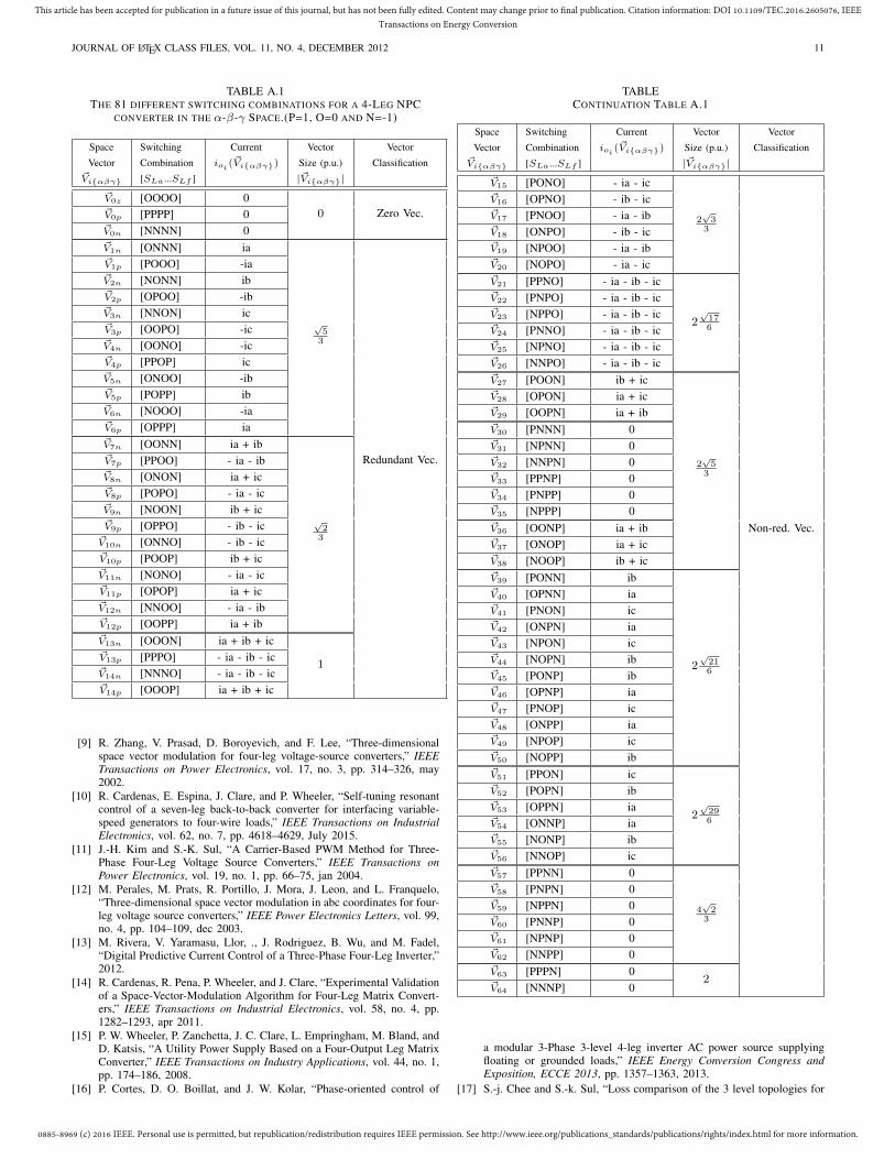
TABLE A.1THE 81 DIFFERENT SWITCHING COMBINATIONS FOR A 4-LEG NPC
CONVERTER IN THE α-β-γ SPACE.(P=1, O=0 AND N=-1)
Space Switching Current Vector Vector
Vector Combination ioi (~Viαβγ) Size (p.u.) Classification
~Viαβγ [SLa...SLf ] |~Viαβγ|~V0z [OOOO] 0
0 Zero Vec.~V0p [PPPP] 0~V0n [NNNN] 0~V1n [ONNN] ia
√53
Redundant Vec.
~V1p [POOO] -ia~V2n [NONN] ib~V2p [OPOO] -ib~V3n [NNON] ic~V3p [OOPO] -ic~V4n [OONO] -ic~V4p [PPOP] ic~V5n [ONOO] -ib~V5p [POPP] ib~V6n [NOOO] -ia~V6p [OPPP] ia~V7n [OONN] ia + ib
√23
~V7p [PPOO] - ia - ib~V8n [ONON] ia + ic~V8p [POPO] - ia - ic~V9n [NOON] ib + ic~V9p [OPPO] - ib - ic~V10n [ONNO] - ib - ic~V10p [POOP] ib + ic~V11n [NONO] - ia - ic~V11p [OPOP] ia + ic~V12n [NNOO] - ia - ib~V12p [OOPP] ia + ib~V13n [OOON] ia + ib + ic
1~V13p [PPPO] - ia - ib - ic~V14n [NNNO] - ia - ib - ic~V14p [OOOP] ia + ib + ic
[9] R. Zhang, V. Prasad, D. Boroyevich, and F. Lee, “Three-dimensionalspace vector modulation for four-leg voltage-source converters,” IEEETransactions on Power Electronics, vol. 17, no. 3, pp. 314–326, may2002.
[10] R. Cardenas, E. Espina, J. Clare, and P. Wheeler, “Self-tuning resonantcontrol of a seven-leg back-to-back converter for interfacing variable-speed generators to four-wire loads,” IEEE Transactions on IndustrialElectronics, vol. 62, no. 7, pp. 4618–4629, July 2015.
[11] J.-H. Kim and S.-K. Sul, “A Carrier-Based PWM Method for Three-Phase Four-Leg Voltage Source Converters,” IEEE Transactions onPower Electronics, vol. 19, no. 1, pp. 66–75, jan 2004.
[12] M. Perales, M. Prats, R. Portillo, J. Mora, J. Leon, and L. Franquelo,“Three-dimensional space vector modulation in abc coordinates for four-leg voltage source converters,” IEEE Power Electronics Letters, vol. 99,no. 4, pp. 104–109, dec 2003.
[13] M. Rivera, V. Yaramasu, Llor, ., J. Rodriguez, B. Wu, and M. Fadel,“Digital Predictive Current Control of a Three-Phase Four-Leg Inverter,”2012.
[14] R. Cardenas, R. Pena, P. Wheeler, and J. Clare, “Experimental Validationof a Space-Vector-Modulation Algorithm for Four-Leg Matrix Convert-ers,” IEEE Transactions on Industrial Electronics, vol. 58, no. 4, pp.1282–1293, apr 2011.
[15] P. W. Wheeler, P. Zanchetta, J. C. Clare, L. Empringham, M. Bland, andD. Katsis, “A Utility Power Supply Based on a Four-Output Leg MatrixConverter,” IEEE Transactions on Industry Applications, vol. 44, no. 1,pp. 174–186, 2008.
[16] P. Cortes, D. O. Boillat, and J. W. Kolar, “Phase-oriented control of
TABLECONTINUATION TABLE A.1
Space Switching Current Vector Vector
Vector Combination ioi (~Viαβγ) Size (p.u.) Classification
~Viαβγ [SLa...SLf ] |~Viαβγ|~V15 [PONO] - ia - ic
2√3
3
~V16 [OPNO] - ib - ic~V17 [PNOO] - ia - ib~V18 [ONPO] - ib - ic~V19 [NPOO] - ia - ib~V20 [NOPO] - ia - ic~V21 [PPNO] - ia - ib - ic
2√176
~V22 [PNPO] - ia - ib - ic~V23 [NPPO] - ia - ib - ic~V24 [PNNO] - ia - ib - ic~V25 [NPNO] - ia - ib - ic~V26 [NNPO] - ia - ib - ic~V27 [POON] ib + ic
2√5
3
~V28 [OPON] ia + ic~V29 [OOPN] ia + ib~V30 [PNNN] 0~V31 [NPNN] 0~V32 [NNPN] 0~V33 [PPNP] 0~V34 [PNPP] 0~V35 [NPPP] 0~V36 [OONP] ia + ib Non-red. Vec.~V37 [ONOP] ia + ic~V38 [NOOP] ib + ic~V39 [PONN] ib
2√216
~V40 [OPNN] ia~V41 [PNON] ic~V42 [ONPN] ia~V43 [NPON] ic~V44 [NOPN] ib~V45 [PONP] ib~V46 [OPNP] ia~V47 [PNOP] ic~V48 [ONPP] ia~V49 [NPOP] ic~V50 [NOPP] ib~V51 [PPON] ic
2√296
~V52 [POPN] ib~V53 [OPPN] ia~V54 [ONNP] ia~V55 [NONP] ib~V56 [NNOP] ic~V57 [PPNN] 0
4√2
3
~V58 [PNPN] 0~V59 [NPPN] 0~V60 [PNNP] 0~V61 [NPNP] 0~V62 [NNPP] 0~V63 [PPPN] 0
2~V64 [NNNP] 0
a modular 3-Phase 3-level 4-leg inverter AC power source supplyingfloating or grounded loads,” IEEE Energy Conversion Congress andExposition, ECCE 2013, pp. 1357–1363, 2013.
[17] S.-j. Chee and S.-k. Sul, “Loss comparison of the 3 level topologies for
0885-8969 (c) 2016 IEEE. Personal use is permitted, but republication/redistribution requires IEEE permission. See http://www.ieee.org/publications_standards/publications/rights/index.html for more information.
This article has been accepted for publication in a future issue of this journal, but has not been fully edited. Content may change prior to final publication. Citation information: DOI 10.1109/TEC.2016.2605076, IEEETransactions on Energy Conversion
JOURNAL OF LATEX CLASS FILES, VOL. 11, NO. 4, DECEMBER 2012 12
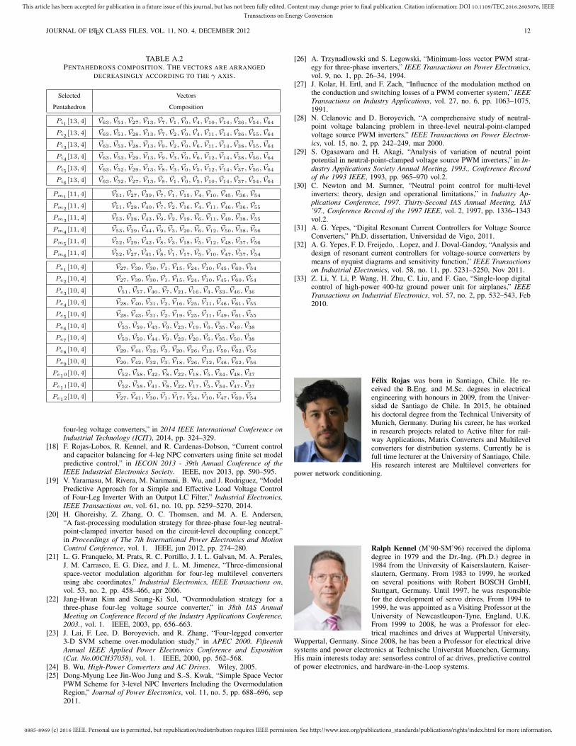
TABLE A.2PENTAHEDRONS COMPOSITION. THE VECTORS ARE ARRANGED
DECREASINGLY ACCORDING TO THE γ AXIS.
Selected Vectors
Pentahedron Composition
Pi1 [13, 4] ~V63, ~V51, ~V27, ~V13, ~V7, ~V1, ~V0, ~V4, ~V10, ~V14, ~V36, ~V54, ~V64
Pi2 [13, 4] ~V63, ~V51, ~V28, ~V13, ~V7, ~V2, ~V0, ~V4, ~V11, ~V14, ~V36, ~V55, ~V64
Pi3 [13, 4] ~V63, ~V53, ~V28, ~V13, ~V9, ~V2, ~V0, ~V6, ~V11, ~V14, ~V38, ~V55, ~V64
Pi4 [13, 4] ~V63, ~V53, ~V29, ~V13, ~V9, ~V3, ~V0, ~V6, ~V12, ~V14, ~V38, ~V56, ~V64
Pi5 [13, 4] ~V63, ~V52, ~V29, ~V13, ~V8, ~V3, ~V0, ~V5, ~V12, ~V14, ~V37, ~V56, ~V64
Pi6 [13, 4] ~V63, ~V52, ~V27, ~V13, ~V8, ~V1, ~V0, ~V5, ~V10, ~V14, ~V37, ~V54, ~V64
Pm1[11, 4] ~V51, ~V27, ~V39, ~V7, ~V1, ~V15, ~V4, ~V10, ~V45, ~V36, ~V54
Pm2[11, 4] ~V51, ~V28, ~V40, ~V7, ~V2, ~V16, ~V4, ~V11, ~V46, ~V36, ~V55
Pm3[11, 4] ~V53, ~V28, ~V43, ~V9, ~V2, ~V19, ~V6, ~V11, ~V49, ~V38, ~V55
Pm4 [11, 4] ~V53, ~V29, ~V44, ~V9, ~V3, ~V20, ~V6, ~V12, ~V50, ~V38, ~V56
Pm5 [11, 4] ~V52, ~V29, ~V42, ~V8, ~V3, ~V18, ~V5, ~V12, ~V48, ~V37, ~V56
Pm6[11, 4] ~V52, ~V27, ~V41, ~V8, ~V1, ~V17, ~V5, ~V10, ~V47, ~V37, ~V54
Pe1 [10, 4] ~V27, ~V39, ~V30, ~V1, ~V15, ~V24, ~V10, ~V45, ~V60, ~V54
Pe2 [10, 4] ~V27, ~V39, ~V30, ~V1, ~V15, ~V24, ~V10, ~V45, ~V60, ~V54
Pe3 [10, 4] ~V51, ~V57, ~V40, ~V7, ~V21, ~V16, ~V4, ~V33, ~V46, ~V36
Pe4 [10, 4] ~V28, ~V40, ~V31, ~V2, ~V16, ~V25, ~V11, ~V46, ~V61, ~V55
Pe5 [10, 4] ~V28, ~V43, ~V31, ~V2, ~V19, ~V25, ~V11, ~V49, ~V61, ~V55
Pe6 [10, 4] ~V53, ~V59, ~V43, ~V9, ~V23, ~V19, ~V6, ~V35, ~V49, ~V38
Pe7 [10, 4] ~V53, ~V59, ~V44, ~V9, ~V23, ~V20, ~V6, ~V35, ~V50, ~V38
Pe8 [10, 4] ~V29, ~V44, ~V32, ~V3, ~V20, ~V26, ~V12, ~V50, ~V62, ~V56
Pe9 [10, 4] ~V29, ~V42, ~V32, ~V3, ~V18, ~V26, ~V12, ~V48, ~V62, ~V56
Pe10[10, 4] ~V52, ~V58, ~V42, ~V8, ~V22, ~V18, ~V5, ~V34, ~V48, ~V37
Pe11[10, 4] ~V52, ~V58, ~V41, ~V8, ~V22, ~V17, ~V5, ~V34, ~V47, ~V37
Pe12[10, 4] ~V27, ~V41, ~V30, ~V1, ~V17, ~V24, ~V10, ~V47, ~V60, ~V54
four-leg voltage converters,” in 2014 IEEE International Conference onIndustrial Technology (ICIT), 2014, pp. 324–329.
[18] F. Rojas-Lobos, R. Kennel, and R. Cardenas-Dobson, “Current controland capacitor balancing for 4-leg NPC converters using finite set modelpredictive control,” in IECON 2013 - 39th Annual Conference of theIEEE Industrial Electronics Society. IEEE, nov 2013, pp. 590–595.
[19] V. Yaramasu, M. Rivera, M. Narimani, B. Wu, and J. Rodriguez, “ModelPredictive Approach for a Simple and Effective Load Voltage Controlof Four-Leg Inverter With an Output LC Filter,” Industrial Electronics,IEEE Transactions on, vol. 61, no. 10, pp. 5259–5270, 2014.
[20] H. Ghoreishy, Z. Zhang, O. C. Thomsen, and M. A. E. Andersen,“A fast-processing modulation strategy for three-phase four-leg neutral-point-clamped inverter based on the circuit-level decoupling concept,”in Proceedings of The 7th International Power Electronics and MotionControl Conference, vol. 1. IEEE, jun 2012, pp. 274–280.
[21] L. G. Franquelo, M. Prats, R. C. Portillo, J. I. L. Galvan, M. A. Perales,J. M. Carrasco, E. G. Diez, and J. L. M. Jimenez, “Three-dimensionalspace-vector modulation algorithm for four-leg multilevel convertersusing abc coordinates,” Industrial Electronics, IEEE Transactions on,vol. 53, no. 2, pp. 458–466, apr 2006.
[22] Jang-Hwan Kim and Seung-Ki Sul, “Overmodulation strategy for athree-phase four-leg voltage source converter,” in 38th IAS AnnualMeeting on Conference Record of the Industry Applications Conference,2003., vol. 1. IEEE, 2003, pp. 656–663.
[23] J. Lai, F. Lee, D. Boroyevich, and R. Zhang, “Four-legged converter3-D SVM scheme over-modulation study,” in APEC 2000. FifteenthAnnual IEEE Applied Power Electronics Conference and Exposition(Cat. No.00CH37058), vol. 1. IEEE, 2000, pp. 562–568.
[24] B. Wu, High-Power Converters and AC Drives. Wiley, 2005.[25] Dong-Myung Lee Jin-Woo Jung and S.-S. Kwak, “Simple Space Vector
PWM Scheme for 3-level NPC Inverters Including the OvermodulationRegion,” Journal of Power Electronics, vol. 11, no. 5, pp. 688–696, sep2011.
[26] A. Trzynadlowski and S. Legowski, “Minimum-loss vector PWM strat-egy for three-phase inverters,” IEEE Transactions on Power Electronics,vol. 9, no. 1, pp. 26–34, 1994.
[27] J. Kolar, H. Ertl, and F. Zach, “Influence of the modulation method onthe conduction and switching losses of a PWM converter system,” IEEETransactions on Industry Applications, vol. 27, no. 6, pp. 1063–1075,1991.
[28] N. Celanovic and D. Boroyevich, “A comprehensive study of neutral-point voltage balancing problem in three-level neutral-point-clampedvoltage source PWM inverters,” IEEE Transactions on Power Electron-ics, vol. 15, no. 2, pp. 242–249, mar 2000.
[29] S. Ogasawara and H. Akagi, “Analysis of variation of neutral pointpotential in neutral-point-clamped voltage source PWM inverters,” in In-dustry Applications Society Annual Meeting, 1993., Conference Recordof the 1993 IEEE, 1993, pp. 965–970 vol.2.
[30] C. Newton and M. Sumner, “Neutral point control for multi-levelinverters: theory, design and operational limitations,” in Industry Ap-plications Conference, 1997. Thirty-Second IAS Annual Meeting, IAS’97., Conference Record of the 1997 IEEE, vol. 2, 1997, pp. 1336–1343vol.2.
[31] A. G. Yepes, “Digital Resonant Current Controllers for Voltage SourceConverters,” Ph.D. dissertation, Universidad de Vigo, 2011.
[32] A. G. Yepes, F. D. Freijedo, . Lopez, and J. Doval-Gandoy, “Analysis anddesign of resonant current controllers for voltage-source converters bymeans of nyquist diagrams and sensitivity function,” IEEE Transactionson Industrial Electronics, vol. 58, no. 11, pp. 5231–5250, Nov 2011.
[33] Z. Li, Y. Li, P. Wang, H. Zhu, C. Liu, and F. Gao, “Single-loop digitalcontrol of high-power 400-hz ground power unit for airplanes,” IEEETransactions on Industrial Electronics, vol. 57, no. 2, pp. 532–543, Feb2010.
Felix Rojas was born in Santiago, Chile. He re-ceived the B.Eng. and M.Sc. degrees in electricalengineering with honours in 2009, from the Univer-sidad de Santiago de Chile. In 2015, he obtainedhis doctoral degree from the Technical University ofMunich, Germany. During his career, he has workedin research projects related to Active filter for rail-way Applications, Matrix Converters and Multilevelconverters for distribution systems. Currently he isfull time lecturer at the University of Santiago, Chile.His research interest are Multilevel converters for
power network conditioning.
Ralph Kennel (M’90-SM’96) received the diplomadegree in 1979 and the Dr.-Ing. (Ph.D.) degree in1984 from the University of Kaiserslautern, Kaiser-slautern, Germany. From 1983 to 1999, he workedon several positions with Robert BOSCH GmbH,Stuttgart, Germany. Until 1997, he was responsiblefor the development of servo drives. From 1994 to1999, he was appointed as a Visiting Professor at theUniversity of Newcastleupon-Tyne, England, U.K.From 1999 to 2008, he was a Professor for elec-trical machines and drives at Wuppertal University,
Wuppertal, Germany. Since 2008, he has been a Professor for electrical drivesystems and power electronics at Technische Universtat Muenchen, Germany.His main interests today are: sensorless control of ac drives, predictive controlof power electronics, and hardware-in-the-Loop systems.
0885-8969 (c) 2016 IEEE. Personal use is permitted, but republication/redistribution requires IEEE permission. See http://www.ieee.org/publications_standards/publications/rights/index.html for more information.
This article has been accepted for publication in a future issue of this journal, but has not been fully edited. Content may change prior to final publication. Citation information: DOI 10.1109/TEC.2016.2605076, IEEETransactions on Energy Conversion
JOURNAL OF LATEX CLASS FILES, VOL. 11, NO. 4, DECEMBER 2012 13
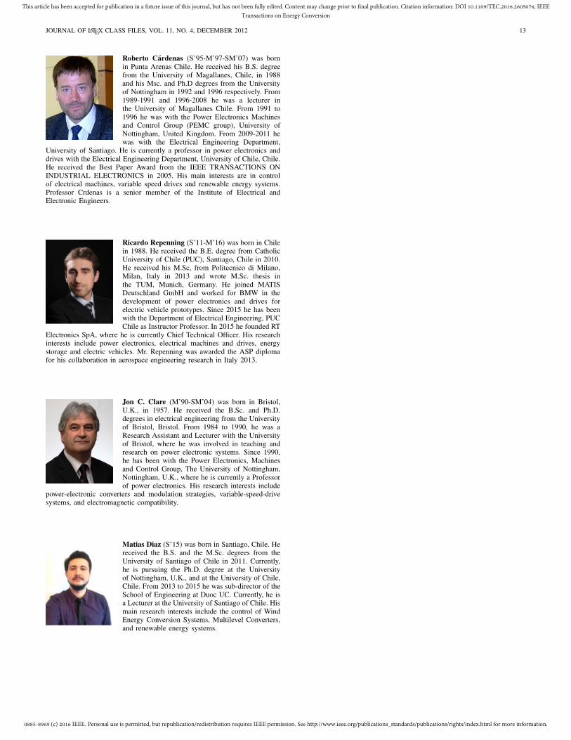
Roberto Cardenas (S’95-M’97-SM’07) was bornin Punta Arenas Chile. He received his B.S. degreefrom the University of Magallanes, Chile, in 1988and his Msc. and Ph.D degrees from the Universityof Nottingham in 1992 and 1996 respectively. From1989-1991 and 1996-2008 he was a lecturer inthe University of Magallanes Chile. From 1991 to1996 he was with the Power Electronics Machinesand Control Group (PEMC group), University ofNottingham, United Kingdom. From 2009-2011 hewas with the Electrical Engineering Department,
University of Santiago. He is currently a professor in power electronics anddrives with the Electrical Engineering Department, University of Chile, Chile.He received the Best Paper Award from the IEEE TRANSACTIONS ONINDUSTRIAL ELECTRONICS in 2005. His main interests are in controlof electrical machines, variable speed drives and renewable energy systems.Professor Crdenas is a senior member of the Institute of Electrical andElectronic Engineers.
Ricardo Repenning (S’11-M’16) was born in Chilein 1988. He received the B.E. degree from CatholicUniversity of Chile (PUC), Santiago, Chile in 2010.He received his M.Sc, from Politecnico di Milano,Milan, Italy in 2013 and wrote M.Sc. thesis inthe TUM, Munich, Germany. He joined MATISDeutschland GmbH and worked for BMW in thedevelopment of power electronics and drives forelectric vehicle prototypes. Since 2015 he has beenwith the Department of Electrical Engineering, PUCChile as Instructor Professor. In 2015 he founded RT
Electronics SpA, where he is currently Chief Technical Officer. His researchinterests include power electronics, electrical machines and drives, energystorage and electric vehicles. Mr. Repenning was awarded the ASP diplomafor his collaboration in aerospace engineering research in Italy 2013.
Jon C. Clare (M’90-SM’04) was born in Bristol,U.K., in 1957. He received the B.Sc. and Ph.D.degrees in electrical engineering from the Universityof Bristol, Bristol. From 1984 to 1990, he was aResearch Assistant and Lecturer with the Universityof Bristol, where he was involved in teaching andresearch on power electronic systems. Since 1990,he has been with the Power Electronics, Machinesand Control Group, The University of Nottingham,Nottingham, U.K., where he is currently a Professorof power electronics. His research interests include
power-electronic converters and modulation strategies, variable-speed-drivesystems, and electromagnetic compatibility.
Matias Diaz (S’15) was born in Santiago, Chile. Hereceived the B.S. and the M.Sc. degrees from theUniversity of Santiago of Chile in 2011. Currently,he is pursuing the Ph.D. degree at the Universityof Nottingham, U.K., and at the University of Chile,Chile. From 2013 to 2015 he was sub-director of theSchool of Engineering at Duoc UC. Currently, he isa Lecturer at the University of Santiago of Chile. Hismain research interests include the control of WindEnergy Conversion Systems, Multilevel Converters,and renewable energy systems.