rt1025ws y ou r power pa rtn er. design notices/media/evb /evb_rt1025_p0/dn_rt1025ws... · ppg (mv)...
TRANSCRIPT

RT1025WS Design Notices
DN_RT1025WS September 2018 1 http://www.richtek.com
your power partner.
RT1025 ECG/PPG AFE Design Notices
Purpose
The RT1025 is an integrated AFE solution for Heart-Rate monitoring and Biopotential measurements. The RT1025
integrate low noise voltage and current sensing channels and is capable of sensing ECG (Electrocardiography) and
PPG (Photoplethysmography) simultaneously. This document describes the design guideline for RT1025 HW
development. It includes the ECG/PPG principle, register programming guide, PCB hardware design notice, and
mechanism design consideration.
Table of Contents
Introduction ............................................................................................................................................................ 2
ECG/PPG Principle ................................................................................................................................................ 3
Register Interface .................................................................................................................................................. 6
SPI Interface Protocol .......................................................................................................................................... 31
Register Programming Guide ............................................................................................................................... 34
PCB and Hardware Design Notice ....................................................................................................................... 38
Product Mechanism Design Consideration ........................................................................................................... 41
More Information.................................................................................................................................................. 43
Important Notice for Richtek Evaluation Board ..................................................................................................... 43
RT1025WS Design Notices
DN_RT1025WS September 2018 2 http://www.richtek.com
your power partner.
Introduction
General Product Information
The RT1025 is an integrated AFE solution for Heart-Rate monitoring and measurements. The RT1025 integrates low
noise voltage and current sensing channels and is capable of sensing ECG (Electrocardiography) and PPG
(Photoplethysmography) simultaneously. The RT1025 have > 100dB dynamic range and can sense pulses
accurately by detecting the heart’s electric signals. The sampling rates of the high-precision voltage and current
sensing channels in the RT1025 are configurable between 64 to 4kHz. The RT1025 solution need only few discrete
components and is easy to use for low-power medical ECG/PPG, sports, and fitness applications. With high levels
of integration and high-precision voltage and current sensing channels, the RT1025 solution is suitable for scalable
medical instrumentation systems. The RT1025 is available in a 3.1mm x 3.4mm, 41-Ball, 0.4mm pitch, WL-CSP
package.
Product Feature
ECG Channel Feature
Supports Two-Electrode (2E) Mode and Right Leg Drive (RLD) Mode
Low Noise PGA and High Resolution ADC
Input Impedance : 125M to 500MΩ at Two-Electrode Mode and > 1GΩ at Right Leg Drive Mode
Low Input-Referred Noise : 0.67µVrms (64Hz ODR, Gain = 12)
Dynamic Range : 110dB at Gain = 6
CMRR > 85dB at 60Hz
Data rate : 64SPS to 4k SPS
PPG Channel Feature
Flexible Timing Control and Support Dynamic Power Down
TX Supports H-bridge and Push/Pull Mode
TX LED Current Range : 10 / 25 / 35 / 50 / 65 / 75 / 90 / 105mA, Each with 8-bit Current Resolution
Input Maximum Current Range : 0.5 to 50μA
Input Maximum Capacitance : 1nF
Input-Referred Noise : 50pArms at 5µA Input Current
CMRR > 80dB at 60Hz
PGA Gain : 1 to 6V/V
Ambient DAC1/DAC2 Range : 1 to 6µA
Others
2-in-1 Bio-Sensing AFE (Voltage/Current)
Built-In Heartbeat Interval Estimation
Integrates an Oscillator to offer High-Precision Clock with External Crystal
Support I2C and SPI I/F for MCU
On-Chip SRAM for Data Buffering
Ultra-Low Power Consumption
Operating Temperature Range : –20°C to 65°C
Small 3.1mm x 3.4mm, 41-Ball, 0.4mm Pitch, and W-LCSP Package
RoHS Compliant and Halogen Free

RT1025WS Design Notices
DN_RT1025WS September 2018 3 http://www.richtek.com
your power partner.
ECG/PPG Principle
Using RT1025 for ECG Sensing
Below figure shows show the analog/digital parts of ECG system. The ECG channel supports two-electrode (2E)
mode and right leg drive (RLD) mode, and acts as a buffer between human and circuit. It integrates a programmable
gain amplifier (PGA), a right leg drive amplifier, and a 24-bit sigma-delta analog-to-digital converter (ADC) to sense
and digitize the ECG signal. The PGA is a differential input/differential output, and has seven gain settings (1, 2, 3,
4, 6, 8, and 12). The sampling frequency of ECG ADC is adjustable from 64Hz to 4096Hz.
Right Leg Drive (RLD) circuit is an electric circuit that is added to biological signal amplifiers to reduce common-
mode interference.
The ECG channel outputs 24 bits of data per channel in binary twos complement format, MSB first. Bit [23] is sign
bit. A positive full-scale input produces an output code of 7FFFFFh and the negative full-scale input produces an
output code of 800000h. The output clips at these codes for signals exceeding full-scale. All 24 bits toggle when the
analog input is at positive or negative full-scale.
23
4VECGADC Outputcode 1000
ECGADC Outputcode LSB 1000 2ECG (mV) ECG Gain ECG Gain

RT1025WS Design Notices
DN_RT1025WS September 2018 4 http://www.richtek.com
your power partner.
Using RT1025 for PPG Sensing
Below figure shows the block diagram for PPG acquisition. The PPG channel is separated into two parts: Transmitter
(TX) and Receiver (RX). The TX part consist of LED driver. The light emitted by LED is penetrated /reflected by the
skin, and received by photodiode of the RX. The RX consists of a trans-impedance amplifier (TIA), a programmable
gain amplifier (PGA), an ambient cancellation digital-to-analog converter (AMBDAC), and a 16-bit incremental ADC.
It amplifies and digitizes the received current.
TIA + PGA PPG
ADC
FIFO/
CIC
LED DRVTiming
mod.
INP_PPG
INN_PPG
TX1
TX2
AMB_DACOptical Module
PPG
Average
LED
Boost
PGA_Gain
TIA_Filter
PPG
SRAM1
PPG
SRAM2
The LED driver and the external voltage boost are used to light up the external LED. The LED full scale current range
is from 10 mA to 105 mA with a 3-bit current step of 15mA via DAC register setting. Push-Pull mode and H-Bridge
mode of the LED driver schemes are supported. Suggest to use Push-Pull LED driving configuration as shown in
below figure. The minimum external supply voltage (LED_SUP) = 0.7V + (maximum voltage drop across the LED).

RT1025WS Design Notices
DN_RT1025WS September 2018 5 http://www.richtek.com
your power partner.
For PPG acquisition, the photo detector transfers the reflected light into current and then amplifies by TIA that
converts the input photodiode current into an appropriate voltage. TIA_Filter was controlled by the register for the
input current low pass filter tuning. PGA_Gain was used to set the PGA Gain. AMB_DAC control the current source
to cancel the ambient light leakage from photo detector. The AMB_DAC has a cancellation current range of 6 μA
with six steps (1 μA each) for two phases (LED1/LED2 phase and AMB1/AMB2 phase). The PGA amplifier gains up
the photo detector input and has five programmable gain settings: 1, 1.5, 2, 3, 4, and 6 (V/V). Then, the signals are
sampled by the corresponding LPFs and digitized by a 16-bit incremental ADC.
The PPG acquisition outputs 24 bits of data per channel in binary twos complement format, MSB first. Bit [22] is sign
bit. A positive full-scale input produces an output code of 3FFFFFh and the negative full-scale input produces an
output code of 400000h. The output clips at these codes for signals exceeding full-scale. All 22 bits toggle when the
analog input is at positive or negative full-scale.
FPD AMB AMB _DAC
16
RPPG (mV) 2 I I I 100K PGA gain
100K
3.2VPPG (mV) PPGADC Outputcode LSB 1000 PPGADC Outputcode 1000
2
The PPG control logic (timing module) can adjust the sampling rate (Equation 5) and duty cycle (Equation 6) of the
LED currents and also power down the AFE when the LEDs are off. The output of the ambient cancellation amplifier
is separated into LED1, AMB1, LED2, AMB2 channels. When LED2 is on, the amplifier output is filtered and sampled
on capacitor CLED2. Similarly, the LED1 signal is sampled on the CLED1 capacitor when LED1 is ON. In between
the LED2 and LED1 pulses, the idle amplifier output is sampled to estimate the ambient signal on capacitors

RT1025WS Design Notices
DN_RT1025WS September 2018 6 http://www.richtek.com
your power partner.
CLED2_amb and CLED1_amb. The minimum supported RX sampling time is 50μs.
1MHz
PRF (Sampling Rate, Hz) 64Hz to 4096HzPRP 1
LED On TimeDuty (%) 1.5% to 25%
PRP 100
Register Interface
The device has a simple register interface which allows an SPI or I2C master to configure and monitor all aspects of
the device. Below table lists an overview of user programmable registers. By convention, bit 0 is the least significant
bit (LSB) of a byte register.
Interrupt Register Interface
Register Module : Reg_0 I2C address : 0x33 or 0x37
SPI address : 0x33
Address Name Width Register Function
0000004C INT_CON 32 Interrupt control register
00000054 INT_STATUS 32 Interrupt status register
PPG Channel Register Interface
Register Module : Reg_0 I2C address : 0x33 or 0x37
SPI address : 0x33
Address Name Width Register Function
00000060 AFE_DIG_ENABLE 32 AFE Digital Part Enable
00000018 PPGFE_CON0 32 PPGFE Control 0
0000001C PPGFE_CON1 32 PPGFE Control 1

RT1025WS Design Notices
DN_RT1025WS September 2018 7 http://www.richtek.com
your power partner.
PPG Channel Register Interface
Register Module : Reg_0 I2C address : 0x33 or 0x37
SPI address : 0x33
Address Name Width Register Function
00000020 PPGADC_CON0 32 PPGADC Control 0
00000028 LEDDRV_CON0 32 LED Driving Control 0
0000002C LEDDRV_CON1 32 LED Driving Control 1
00000068 AFE_PPG_CON 32 PPG Digital Part Control
000000D0 PPG1_SRAM_CON4 32 PPG1 SRAM Control 0
000000D4 PPG1_SRAM _CON5 32 PPG1 SRAM Control 1
000000D8 PPG1_SRAM _CON6 32 PPG1 SRAM Control 2
000000DC PPG1_SRAM _CON7 32 PPG1 SRAM Control 3
000000E0 PPG2_SRAM _CON8 32 PPG2 SRAM Control 0
000000E4 PPG2_SRAM _CON9 32 PPG2 SRAM Control 1
000000E8 PPG2_SRAM _CON10 32 PPG2 SRAM Control 2
000000EC PPG2_SRAM _CON11 32 PPG2 SRAM Control 3
PPG Channel Timing Control Register Interface
Register Module : Reg_1 I2C address : 0x23 or 0x27
SPI address : 0x23
Address Name Width Register Function
00000028 AFE_TCTRL_CON0 32 Timing Control Module Control 0
0000002C AFE_TCTRL_CON1 32 Timing Control Module Control 1
00000030 AFE_TCTRL_CON2 32 Timing Control Module Control 2
00000034 AFE_TCTRL_CON3 32 Timing Control Module Control 3
00000038 AFE_TCTRL_CON4 32 Timing Control Module Control 4
0000003C AFE_TCTRL_CON5 32 Timing Control Module Control 5
00000040 AFE_TCTRL_CON6 32 Timing Control Module Control 6
00000044 AFE_TCTRL_CON7 32 Timing Control Module Control 7
00000048 AFE_TCTRL_CON8 32 Timing Control Module Control 8
0000004C AFE_TCTRL_CON9 32 Timing Control Module Control 9
00000050 AFE_TCTRL_CON10 32 Timing Control Module Control 10
00000054 AFE_TCTRL_CON11 32 Timing Control Module Control 11
00000058 AFE_TCTRL_CON12 32 Timing Control Module Control 12
0000005C AFE_TCTRL_CON13 32 Timing Control Module Control 13
00000060 AFE_TCTRL_CON14 32 Timing Control Module Control 14
00000064 AFE_TCTRL_CON15 32 Timing Control Module Control 15
00000068 AFE_TCTRL_CON16 32 Timing Control Module Control 16
0000006C AFE_TCTRL_CON17 32 Timing Control Module Control 17
00000070 AFE_TCTRL_CON18 32 Timing Control Module Control 18

RT1025WS Design Notices
DN_RT1025WS September 2018 8 http://www.richtek.com
your power partner.
ECG Channel Register Interface
Register Module : Reg_0 I2C address : 0x33 or 0x37
SPI address : 0x33
Address Name Width Register Function
00000008 ECGFE_CON0 32 ECGFE Control
00000010 ECGADC_CON0 32 ECGADC Control
00000064 AFE_ECG_CON 32 ECG Digital Part Control
000000C0 ECG_SRAM_CON0 32 ECG SRAM Control 0
000000C4 ECG_SRAM_CON1 32 ECG SRAM Control 1
000000C8 ECG_SRAM_CON2 32 ECG SRAM Control 2
000000CC ECG_SRAM_CON3 32 ECG SRAM Control 3
HBI Estimation Register Interface
Register Module : Reg_0 I2C address : 0x33 or 0x37
SPI address : 0x33
Address Name Width Register Function
000000F0 HBI_SRAM_CON12 32 HBI SRAM Control 0
000000F4 HBI_SRAM_CON13 32 HBI SRAM Control 1
000000F8 HBI_SRAM_CON14 32 HBI SRAM Control 2
000000FC HBI_SRAM_CON15 32 HBI SRAM Control 3
Interrupts
To facilitate MCU programming and sensor data flow control, RT1025 supports various interrupts for each function.
The INT_CON register enables or disables interrupts on various events. Host MCU can identify the exact cause of
interrupt by reading the INT_STATUS register. Below table lists supported interrupts and their usage.
Interrupt Description
SRAM_ECG ECG SRAM threshold level is reached
SRAM_ECG_WFULL ECG SRAM is full.
SRAM_ECG_REMPTY ECG SRAM is empty
SRAM_PPG1 PPG1 SRAM threshold level is reached
SRAM_PPG1_WFULL PPG1 SRAM is full.
SRAM_PPG1_REMPTY PPG1 SRAM is empty
SRAM_PPG2 PPG2 SRAM threshold level is reached
SRAM_PPG2_WFULL PPG2 SRAM is full.
SRAM_PPG2_REMPTY PPG2 SRAM is empty
SRAM_HBI HBI SRAM threshold level is reached
SRAM_HBI_WFULL HBI SRAM is full.
SRAM_HBI_REMPTY HBI SRAM is empty

RT1025WS Design Notices
DN_RT1025WS September 2018 9 http://www.richtek.com
your power partner.
Interrupts - Register Definitions
The interrupts status has a simple register interface which allows an SPI or I2C master to configure and monitor all
aspects of the device.
Register Module : Reg_0 I2C address : 0x33 or 0x37
SPI address : 0x33
Address Name Width Register Function
0000004C INT_CON 32 Interrupt control register
00000054 INT_STATUS 32 Interrupt status register
(REG_0, 0x0000004C) INT_CON : Interrupt Control Register
This register is used to enable the interrupts
Name Function Address Reset
INT_CON Interrupt Control REG_0,
0x4C 00000000h
Bit Mode Name Reset
Value Description
[31:28] RW RESV 0 Reserved
[27:24] RESV Reserved
[23:16] RW RESV 0 Reserved
15 RW INT_POLARITY 0
Interrupt level inverting
0 : Do not invert interrupt source.
1 : Invert interrupt source.
[14:13] RESV Reserved
12 RW INT_EN_SRAM_HBI_REMPTY 0
HBI SRAM empty interrupt enable
0 : No interrupt, when the HBI SRAM is
empty.
1 : Interrupting, when the HBI SRAM is
empty.
11 RW INT_EN_SRAM_HBI_WFULL 0
HBI SRAM full interrupt enable
0 : No interrupt, when the HBI SRAM is full.
1 : Interrupting, when the HBI SRAM is full.
10 RW INT_EN_SRAM_HBI 0
HBI SRAM threshold interrupt enable
(Threshold level : HBI_SRAM_CON15::
IRG_TH[8:0])
0 : No interrupt, when the HBI SRAM
threshold level is reached.
1 : Interrupting, when the HBI SRAM
threshold level is reached.
9 RW INT_EN_SRAM_PPG2_REMPTY 0
PPG2 SRAM empty interrupt enable
0 : No interrupt, when the PPG2 SRAM is
empty.
1 : Interrupting, when the PPG2 SRAM is
empty.

RT1025WS Design Notices
DN_RT1025WS September 2018 10 http://www.richtek.com
your power partner.
Name Function Address Reset
INT_CON Interrupt Control REG_0,
0x4C 00000000h
Bit Mode Name Reset
Value Description
8 RW INT_EN_SRAM_PPG2_WFULL 0
PPG2 SRAM full interrupt enable
0 : No interrupt, when the PPG2 SRAM is
full.
1 : Interrupting, when the PPG2 SRAM is
full.
7 RW INT_EN_SRAM_PPG2 0
PPG2 SRAM threshold interrupt enable
(Threshold level : PPG2_SRAM_CON11::
IRG_TH[8:0])
0 : No interrupt, when the PPG2 SRAM
threshold level is reached.
1 : Interrupting, when the PPG2 SRAM
threshold level is reached.
6 RW INT_EN_SRAM_PPG1_REMPTY 0
PPG1 SRAM empty interrupt enable
0 : No interrupt, when the PPG1 SRAM is
empty.
1 : Interrupting, when the PPG1 SRAM is
empty.
5 RW INT_EN_SRAM_PPG1_WFULL 0
PPG1 SRAM full interrupt enable
0 : No interrupt, when the PPG1 SRAM is
full.
1 : Interrupting, when the PPG1 SRAM is
full.
4 RW INT_EN_SRAM_PPG1 0
PPG1 SRAM threshold interrupt enable
(Threshold level : PPG1_SRAM_CON7::
IRG_TH[8:0])
0 : No interrupt, when the PPG1 SRAM
threshold level is reached.
1 : Interrupting, when the PPG1 SRAM
threshold level is reached.
3 RW INT_EN_SRAM_ECG_REMPTY 0
ECG SRAM empty interrupt enable
0 : No interrupt, when the ECG SRAM is
empty.
1 : Interrupting, when the ECG SRAM is
empty.
2 RW INT_EN_SRAM_ECG_WFULL 0
ECG SRAM full interrupt enable
0 : No interrupt, when the ECG SRAM is full.
1 : Interrupting, when the ECG SRAM is full.
1 RW INT_EN_SRAM_ECG 0
ECG SRAM threshold interrupt enable
(Threshold level :
ECG_SRAM_CON3::IRG_TH[8:0])
0 : No interrupt, when the ECG SRAM
threshold level is reached.
1 : Interrupting, when the ECG SRAM
threshold level is reached.
0 RW RESV 0 Reserved

RT1025WS Design Notices
DN_RT1025WS September 2018 11 http://www.richtek.com
your power partner.
(REG_0, 0x00000054) INT_STATUS : Interrupt Status Register
This register is used to check the interrupts status. To clear a specific interrupt, INT_EN_* control bit should be set
to 0 and INT_CLR_* clear bit should be set to 1 then set to 0.
Name Function Address Reset
INT_STATUS Interrupt Status REG_0,
0x54 FFFFFFFFh
Bit Mode Name Reset
Value Description
[31:29] RESV Reserved
28 RW INT_CLR_SRAM_HBI_REMPTY 0 Clear HBI SRAM empty interrupt.
27 RW INT_CLR_SRAM_HBI_WFULL 0 Clear HBI SRAM full interrupt.
26 RW INT_CLR_SRAM_HBI 0 Clear HBI SRAM threshold interrupt.
25 RW INT_CLR_SRAM_PPG2_REMPTY 0 Clear PPG2 SRAM empty interrupt.
24 RW INT_CLR_SRAM_PPG2_WFULL 0 Clear PPG2 SRAM full interrupt.
23 RW INT_CLR_SRAM_PPG2 0 Clear PPG2 SRAM threshold interrupt.
22 RW INT_CLR_SRAM_PPG1_REMPTY 0 Clear PPG1 SRAM empty interrupt.
21 RW INT_CLR_SRAM_PPG1_WFULL 0 Clear PPG1 SRAM full interrupt.
20 RW INT_CLR_SRAM_PPG1 0 Clear PPG1 SRAM threshold interrupt.
19 RW INT_CLR_SRAM_ECG_REMPTY 0 Clear ECG SRAM empty interrupt.
18 RW INT_CLR_SRAM_ECG_WFULL 0 Clear ECG SRAM full interrupt.
17 RW INT_CLR_SRAM_ECG 0 Clear ECG SRAM threshold interrupt.
16 RW RESV 0 Reserved
[15:13] RESV Reserved
12 R INT_STATUS_SRAM_HBI_REMP
TY X Status of HBI SRAM empty interrupt.
11 R INT_STATUS_SRAM_HBI_WFULL X Status of HBI SRAM full interrupt.
10 R INT_STATUS_SRAM_HBI X Status of HBI SRAM threshold interrupt.
9 R INT_STATUS_SRAM_PPG2_REM
PTY X Status of PPG2 SRAM empty interrupt.
8 R INT_STATUS_SRAM_PPG2_WFU
LL X Status of PPG2 SRAM full interrupt.
7 R INT_STATUS_SRAM_PPG2 X Status of PPG2 SRAM threshold interrupt.
6 R INT_STATUS_SRAM_PPG1_REM
PTY X Status of PPG1 SRAM empty interrupt.
5 R INT_STATUS_SRAM_PPG1_WFU
LL X Status of PPG1 SRAM full interrupt.
4 R INT_STATUS_SRAM_PPG1 X Status of PPG1 SRAM threshold interrupt.
3 R INT_STATUS_SRAM_ECG_REMP
TY X Status of ECG SRAM empty interrupt.
2 R INT_STATUS_SRAM_ECG_WFUL
L X Status of ECG SRAM full interrupt.
1 R INT_STATUS_SRAM_ECG X Status of ECG SRAM threshold interrupt.

RT1025WS Design Notices
DN_RT1025WS September 2018 12 http://www.richtek.com
your power partner.
Name Function Address Reset
INT_STATUS Interrupt Status REG_0,
0x54 FFFFFFFFh
Bit Mode Name Reset
Value Description
0 R RESV X Reserved.
ECG Channel - Register Definitions
The ECG channel has a simple register interface which allows an SPI or I2C master to configure and monitor all
aspects of the device.
Register Module : Reg_0 I2C address : 0x33 or 0x37
SPI address : 0x33
Address Name Width Register Function
00000008 ECGFE_CON0 32 ECGFE Control
00000010 ECGADC_CON0 32 ECGADC Control
00000064 AFE_ECG_CON 32 ECG Digital Part Control
000000C0 ECG_SRAM_CON0 32 ECG SRAM Control 0
000000C4 ECG_SRAM_CON1 32 ECG SRAM Control 1
000000C8 ECG_SRAM_CON2 32 ECG SRAM Control 2
000000CC ECG_SRAM_CON3 32 ECG SRAM Control 3
(REG_0, 0x00000008) ECGFE_CON0 : ECGFE Control
This register is used to select the ECG AFE for input impedance adjustment, RLD mode control, and PGA gain
adjustment.
Name Function Address Reset
ECGFE_CON0 ECGFE Control REG_0,
0x08 010AD443h
Bit Mode Name Reset
Value Description
[31:16] RESV Reserved
[15:14] RW RL_ZIN [1:0] 11
Input impedance adjustment (Only @ 2E
mode)
11 : Zin = 500M (default)
10/01 : Zin = 250M
00 : Zin = 125M
[13:11] RESV Reserved
10 RW RL_MODE 1
2E or RLD mode control.
1 : 2E mode
0 : RLD mode (default)
[9: 8] RESV Reserved

RT1025WS Design Notices
DN_RT1025WS September 2018 13 http://www.richtek.com
your power partner.
Name Function Address Reset
ECGFE_CON0 ECGFE Control REG_0,
0x08 010AD443h
Bit Mode Name Reset
Value Description
[7: 4] RW IA_GAIN 0100
PGA gain adjustment (V/V)
0000 : 1
0001 : 2
0010 : 3
0011 : 4
0100 : 6 (default)
0101 : 8
0110 : 12
[3:1] RESV Reserved
0 RW ECGFE_PD 1
ECGFE power down :
1 : Power down
0 : Power on
(REG_0, 0x00000010) ECGADC_CON0 : ECGADC Control
This register is used to control the ECG ADC
Name Function Address Reset
ECGADC_CON0 ECGADC Control REG_0,
0x10 002F5555h
Bit Mode Name Reset
Value Description
[31:21] RESV Reserved
[20:18] RW ECGADC_FS [2:0] 011
ECGADC FS select :
000 : fs = 64Hz
001 : fs = 128Hz
010 : fs = 256Hz
011 : fs = 512 or 1024 or 2048 or 4096 Hz
Set corresponding ECG_DIG_FS [2:0] at the
same time.
[17:1] RESV Reserved
0 RW ECGADC_PD 1
ECGADC power down :
1 : Power down
0 : Power on

RT1025WS Design Notices
DN_RT1025WS September 2018 14 http://www.richtek.com
your power partner.
(REG_0, 0x00000064) AFE_ECG_CON : ECG Digital Part Control
This register is used to control the ECG digital block
Name Function Address Reset
AFE_ECG_CON ECG Digital Part Control REG_0,
0x64 0000000Bh
Bit Mode Name Reset
Value Description
[31:6] RESV Reserved
[5:3] RW ECG_SRAM [2:0] 001 ECG SRAM start point
[2:0] RW ECG_DIG_FS 011
ECG_DIG FS select :
000 : fs = 64Hz
001 : fs = 128Hz
010 : fs = 256Hz
011 : fs = 512HZ
100 : fs = 1024Hz
101 : fs = 2048HZ
110 : fs = 4096HZ
Set corresponding ECGADC_FS [2:0] at the
same time.
(REG_0, 0x000000C0) ECG_SRAM_CON0 : ECG SRAM Control 0
This register is used to set up the ECG SRAM control
Name Function Address Reset
AFE_ECG_CON ECG Digital Part Control REG_0,
0xC0 00000000h
Bit Mode Name Reset
Value Description
31 RW KSRAM_CE 0 ECG SRAM chip select
30 RW KSRAM_RW_ADDR_AUTO_INC 0
Automatically increase I2C/SPI access ECG
SRAM address
0 : No effect.
1 : Automatically increase.
29 RW KSRAM_ATRIG 0
Enable access ECG SRAM from I2C/SPI
0 : No effect.
1 : Toggle access trigger.
28 RESV Reserved
27 R KSRAM_WTRIG 0
Write ECG SRAM from I2C/SPI
0 : No effect.
1 : Write trigger.
26 R KSRAM_RTRIG 0
Read ECG SRAM from I2C/SPI
0 : No effect.
1 : Read trigger.
[25:16] R KSRAM_CUR_ADDR [9:0] 000h The current access address of ECG SRAM
from I2C/SPI.
[15:10] RESV Reserved
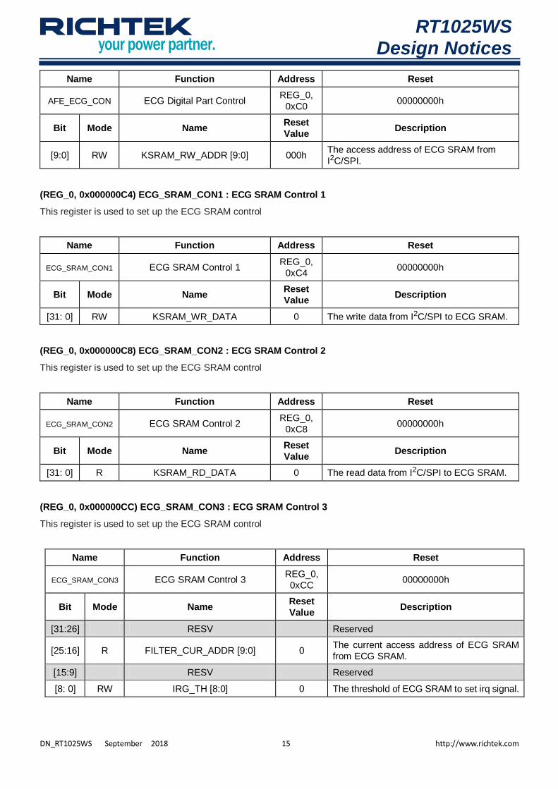
RT1025WS Design Notices
DN_RT1025WS September 2018 15 http://www.richtek.com
your power partner.
Name Function Address Reset
AFE_ECG_CON ECG Digital Part Control REG_0,
0xC0 00000000h
Bit Mode Name Reset
Value Description
[9:0] RW KSRAM_RW_ADDR [9:0] 000h The access address of ECG SRAM from
I2C/SPI.
(REG_0, 0x000000C4) ECG_SRAM_CON1 : ECG SRAM Control 1
This register is used to set up the ECG SRAM control
Name Function Address Reset
ECG_SRAM_CON1 ECG SRAM Control 1 REG_0,
0xC4 00000000h
Bit Mode Name Reset
Value Description
[31: 0] RW KSRAM_WR_DATA 0 The write data from I2C/SPI to ECG SRAM.
(REG_0, 0x000000C8) ECG_SRAM_CON2 : ECG SRAM Control 2
This register is used to set up the ECG SRAM control
Name Function Address Reset
ECG_SRAM_CON2 ECG SRAM Control 2 REG_0,
0xC8 00000000h
Bit Mode Name Reset
Value Description
[31: 0] R KSRAM_RD_DATA 0 The read data from I2C/SPI to ECG SRAM.
(REG_0, 0x000000CC) ECG_SRAM_CON3 : ECG SRAM Control 3
This register is used to set up the ECG SRAM control
Name Function Address Reset
ECG_SRAM_CON3 ECG SRAM Control 3 REG_0,
0xCC 00000000h
Bit Mode Name Reset
Value Description
[31:26] RESV Reserved
[25:16] R FILTER_CUR_ADDR [9:0] 0 The current access address of ECG SRAM
from ECG SRAM.
[15:9] RESV Reserved
[8: 0] RW IRG_TH [8:0] 0 The threshold of ECG SRAM to set irq signal.

RT1025WS Design Notices
DN_RT1025WS September 2018 16 http://www.richtek.com
your power partner.
PPG Channel - Register Definitions
The PPG channel has a simple register interface which allows an SPI or I2C master to configure and monitor all
aspects of the device.
Register Module : Reg_0 I2C address : 0x33 or 0x37
SPI address : 0x33
Address Name Width Register Function
00000060 AFE_DIG_ENABLE 32 AFE Digital Part Enable
00000018 PPGFE_CON0 32 PPGFE Control 0
0000001C PPGFE_CON1 32 PPGFE Control 1
00000020 PPGADC_CON0 32 PPGADC Control 0
00000028 LEDDRV_CON0 32 LED Driving Control 0
0000002C LEDDRV_CON1 32 LED Driving Control 1
00000068 AFE_PPG_CON 32 PPG Digital Part Control
000000D0 PPG1_SRAM_CON4 32 PPG1 SRAM Control 0
000000D4 PPG1_SRAM_CON5 32 PPG1 SRAM Control 1
000000D8 PPG1_SRAM_CON6 32 PPG1 SRAM Control 2
000000DC PPG1_SRAM_CON7 32 PPG1 SRAM Control 3
000000E0 PPG2_SRAM_CON8 32 PPG2 SRAM Control 0
000000E4 PPG2_SRAM_CON9 32 PPG2 SRAM Control 1
000000E8 PPG2_SRAM_CON10 32 PPG2 SRAM Control 2
000000EC PPG2_SRAM_CON11 32 PPG2 SRAM Control 3
Register Module : Reg_1 I2C address : 0x23 or 0x27
SPI address : 0x23
Address Name Width Register Function
00000028 AFE_TCTRL_CON0 32 Timing Control Module Control 0
0000002C AFE_TCTRL_CON1 32 Timing Control Module Control 1
00000030 AFE_TCTRL_CON2 32 Timing Control Module Control 2
00000034 AFE_TCTRL_CON3 32 Timing Control Module Control 3
00000038 AFE_TCTRL_CON4 32 Timing Control Module Control 4
0000003C AFE_TCTRL_CON5 32 Timing Control Module Control 5
00000040 AFE_TCTRL_CON6 32 Timing Control Module Control 6
00000044 AFE_TCTRL_CON7 32 Timing Control Module Control 7
00000048 AFE_TCTRL_CON8 32 Timing Control Module Control 8
0000004C AFE_TCTRL_CON9 32 Timing Control Module Control 9
00000050 AFE_TCTRL_CON10 32 Timing Control Module Control 10
00000054 AFE_TCTRL_CON11 32 Timing Control Module Control 11
00000058 AFE_TCTRL_CON12 32 Timing Control Module Control 12
0000005C AFE_TCTRL_CON13 32 Timing Control Module Control 13

RT1025WS Design Notices
DN_RT1025WS September 2018 17 http://www.richtek.com
your power partner.
Register Module : Reg_1 I2C address : 0x23 or 0x27
SPI address : 0x23
Address Name Width Register Function
00000060 AFE_TCTRL_CON14 32 Timing Control Module Control 14
00000064 AFE_TCTRL_CON15 32 Timing Control Module Control 15
00000068 AFE_TCTRL_CON16 32 Timing Control Module Control 16
0000006C AFE_TCTRL_CON17 32 Timing Control Module Control 17
00000070 AFE_TCTRL_CON18 32 Timing Control Module Control 18
(REG_0, 0x00000060) AFE_DIG_ENABLE : AFE Digital Part Enable
This register is used to enable the AFE blocks and SRAM memory
Name Function Address Reset
AFE_DIG_ENABLE AFE Digital Part Enable REG_0,
0x60 00000000h
Bit Mode Name Reset
Value Description
[31:16] RESV Reserved
[15:11] RESV Reserved
10 RW P2S_MON_EN 0 Enable P2S monitor module.
9 RESV Reserved
8 RW TIMING_EN 0 Enable timing module.
7 RW HBI_SRAM_EN 0 Enable HBI SRAM.
6 RW PPG2_SRAM_EN 0 Enable PPG2 SRAM.
5 RW PPG1_SRAM_EN 0 Enable PPG1 SRAM.
4 RW ECG_SRAM_EN 0 Enable ECG SRAM.
3 RW ECG_EN 0 Enable ECG circuit.
2 RW PPG_EN 0 Enable PPG circuit.
1 RESV Reserved
0 RW HBI_EN 0 Enable HBI circuit.
(REG_0, 0x00000018) PPGFE_CON0 : PPGFE Control 0
This register is used to select the PPG AFE low pass filter bandwidth, PGA gain and ambient current cancellation
Name Function Address Reset
PPGFE_CON0 PPGFE Control 0 REG_0,
0x18 70244212h
Bit Mode Name Reset
Value Description
31 RESV Reserved

RT1025WS Design Notices
DN_RT1025WS September 2018 18 http://www.richtek.com
your power partner.
Name Function Address Reset
PPGFE_CON0 PPGFE Control 0 REG_0,
0x18 70244212h
Bit Mode Name Reset
Value Description
30 RW PPG_PD 1
PPG power down
1 : Power down
0 : Power on
[29:28] RW PPG_LPF_CT [1:0] 11
PPG LPF corner adjustment
11 : 500Hz (default)
10 : 1kHz
01 : 2kHz
00 : 4kHz
[27:25] RW AMB_DAC2 [2:0] 000
AMB phase current adjustment
000 / 001 : 1µA
010 : 2µA
011 : 3µA
100 : 4µA
101 : 5µA
110 : 6µA
[24:22] RW AMB_DAC1 [2:0] 000
LED phase current adjustment
000 / 001 : 1µA
010 : 2µA
011 : 3µA
100 : 4µA
101 : 5µA
110 : 6µA
21 RESV Reserved
[20:18] RW PGA_GAIN [2:0] 001
PGA gain adjustment (V/V)
111 / 110 / 101 : 6
100 : 4
011 : 3
010 : 2
001 : 1.5 (default)
000 : 1
17 RW PPG_ENSEPGAIN 0
Enable separate gain for LED1 phase and
LED2 phase :
1 : Enable
0 : Disable
16 RESV Reserved
[15:11] RW TIA_CF2 [4:0] 01000
TIA CF adjustment for LED2 phase and
AMB2 phase if PPG_ENSEPGAIN=H
Bit_4=1 : +150pF
Bit_3=1 : +50pF
Bit_2=1 : +25pF
Bit_1=1 : +15pF
Bit_0=1 : +5pF
00000 : 5pF

RT1025WS Design Notices
DN_RT1025WS September 2018 19 http://www.richtek.com
your power partner.
Name Function Address Reset
PPGFE_CON0 PPGFE Control 0 REG_0,
0x18 70244212h
Bit Mode Name Reset
Value Description
[10:6] RW TIA_CF1 [4:0] 01000
TIA CF adjustment for LED1 phase and
AMB1 phase
Bit_4=1 : +150pF
Bit_3=1 : +50pF
Bit_2=1 : +25pF
Bit_1=1 : +15pF
Bit_0=1 : +5pF
00000 : 5pF
[5:3] RW TIA_RF2 [2:0] 010
TIA RF adjustment for LED2 phase and
AMB2 phase if PPG_ENSEPGAIN=H
111 / 110 : 1M
101 : 10k
100 : 25k
011 : 50k
010 : 100k
001 : 250k
000 : 500k
[2:0] RW TIA_RF1 [2:0] 010
TIA RF adjustment for LED1 phase and
AMB1 phase
111 / 110 : 1M
101 : 10k
100 : 25k
011 : 50k
010 : 100k
001 : 250k
000 : 500k
(REG_0, 0x0000001C) PPGFE_CON1 : PPGFE Control 1
This register is used to select the PPG AFE AMB_DAC
Name Function Address Reset
PPGFE_CON1 PPGFE Control 1 REG_0,
0x1C 0048CC29h
Bit Mode Name Reset
Value Description
[31:12] RESV Reserved
11 RW AMBDAC_PWDB 1
AMBDAC power down
1 : Power on
0 : Power down, also need to set
PPGFE_CON0::AMBDAC1[2:0] = 0
PPGFE_CON0::AMBDAC2[2:0] = 0
[10:0] RESV Reserved

RT1025WS Design Notices
DN_RT1025WS September 2018 20 http://www.richtek.com
your power partner.
(REG_0, 0x00000020) PPGADC_CON0 : PPGADC Control 0
This register is used to select the PPG ADC
Name Function Address Reset
PPGADC_CON0 PPGADC Control 0 REG_0,
0x20 000F5555h
Bit Mode Name Reset
Value Description
[31:1] RESV Reserved
0 RW PPGADC_PD 1
PPGADC power down
1 : Power down
0 : Power on
(REG_0, 0x00000028) LEDDRV_CON0 : LED Driving Control 0
This register is used to select the LED Driving block
Name Function Address Reset
LEDDRV_CON0 LED Driving Control 0 REG_0,
0x28 00002900h
Bit Mode Name Reset
Value Description
[31:8] RESV Reserved
[7:5] RW TX_Sel[2:0] 000
Full-scale range of LED current
000 : 10mA
001 : 25mA
010 : 35mA
011 : 50mA
100 : 65mA
101 : 75mA
110 : 90mA
111 : 105mA
[4:1] RESV Reserved
0 RW TX_HBrig_PP 0
LED driver scheme
1 : H-bridge mode
0 : Push-pull mode
(REG_0, 0x0000002C) LEDDRV_CON1 : LED Driving Control 1
This register is used to set up the LED Driving block
Name Function Address Reset
LEDDRV_CON1 LED Driving Control 1 REG_0,
0x2C 00002020h
Bit Mode Name Reset
Value Description
[31:16] RESV Reserved

RT1025WS Design Notices
DN_RT1025WS September 2018 21 http://www.richtek.com
your power partner.
Name Function Address Reset
LEDDRV_CON1 LED Driving Control 1 REG_0,
0x2C 00002020h
Bit Mode Name Reset
Value Description
[15:8] RW TX_B2 [7:0] 20h
LED2 current (TX2) DAC2 code
Full scale LED currentLED2 Current DAC2 Code
256
00000000 : Minimum
11111111 : Maximum
[7:0] RW TX_B1 [7:0] 20h
LED1 current (TX1) DAC1 code
Full scale LED currentLED1Current DAC1Code
256
00000000 : Minimum
11111111 : Maximum
(REG_0, 0x00000068) AFE_PPG_CON : PPG Digital Part Control
This register is used to set up the PPG channel digital control
Name Function Address Reset
AFE_PPG_CO
N PPG Digital Part Control
REG_0,
0x68 04B6270Ah
Bit Mode Name Reset
Value Description
[31:26] RW PPG_AVG [5:0] 0000001 Number of average in PPGAVG.
[25:23] RW PPG_SRAM [2:0] 001 PPG SRAM start point.
[22:21] RW Reg5_MIN [1:0] 01 Set minuend of reg5, default = reg2
[20:19] RW Reg5_SUB [1:0] 10 Set subtrahend of reg5, default = reg3
[18:17] RW Reg6_MIN [1:0] 11 Set minuend of reg5, default = reg4
[16:15] RW Reg6_SUB [1:0] 00 Set subtrahend of reg5, default = reg1
[14:12] RW L1_Reg [2:0] 010 Set L1 register, default = reg2
[11:9] RW L2_Reg [2:0] 011 Set L2 register, default = reg3
[8:6] RW L3_Reg [2:0] 100 Set L3 register, default = reg4
[5:3] RW L4_Reg [2:0] 001 Set L4 register, default = reg1
[2:0] RW HBI_Reg [2:0] 010 Set HBI register, default = reg2

RT1025WS Design Notices
DN_RT1025WS September 2018 22 http://www.richtek.com
your power partner.
(REG_0, 0x000000D0) PPG1_SRAM_CON4 : PPG1 SRAM Control 0
This register is used to set up the PPG1 SRAM control
Name Function Address Reset
PPG1_SRAM_CON4
PPG1 SRAM Control 0 REG_0,
0xD0 00000000h
Bit Mode Name Reset
Value Description
31 RW PSRAM_CE 0 PPG1 SRAM chip select
30 RW PSRAM_RW_ADDR_AUTO_INC 0
Automatically increase I2C/SPI access PPG1
SRAM address
0 : No effect.
1 : Automatically increase.
29 RW PSRAM_ATRIG 0
Enable access PPG1 SRAM from I2C/SPI
0 : No effect.
1 : Toggle access trigger.
28 RESV Reserved
27 R PSRAM_WTRIG 0
Write PPG1 SRAM from I2C/SPI
0 : No effect.
1 : Write trigger.
26 R PSRAM_RTRIG 0
Read PPG1 SRAM from I2C/SPI
0 : No effect.
1 : Read trigger.
[25:16] R PSRAM_CUR_ADDR [9:0] 0 The current access address of PPG1 SRAM
from I2C/SPI.
[15:10] RESV Reserved
[9:0] RW UPSRAM_RW_ADDR [9:0] 0 The access address of PPG1 SRAM from
I2C/SPI.
(REG_0, 0x000000D4) PPG1_SRAM_CON5 : PPG1 SRAM Control 1
This register is used to set up the PPG1 SRAM control
Name Function Address Reset
PPG1_SRAM_CON5
PPG1 SRAM Control 1 REG_0,
0xD4 00000000h
Bit Mode Name Reset
Value Description
[31: 0] RW PSRAM_WR_DATA 0h The write data from I2C/SPI to PPG1 SRAM.

RT1025WS Design Notices
DN_RT1025WS September 2018 23 http://www.richtek.com
your power partner.
(REG_0, 0x000000D8) PPG1_SRAM_CON6 : PPG1 SRAM Control 2
This register is used to set up the PPG1 SRAM control
Name Function Address Reset
PPG1_SRAM_CON6
PPG1 SRAM Control 2 REG_0,
0xD8 00000000h
Bit Mode Name Reset
Value Description
[31: 0] R PSRAM_RD_DATA 0h The read data from I2C/SPI to PPG1 SRAM.
(REG_0, 0x000000DC) PPG1_SRAM_CON7 : PPG1 SRAM Control 3
This register is used to set up the PPG1 SRAM control
Name Function Address Reset
PPG1_SRAM_CON7
PPG1 SRAM Control 3 REG_0,
0xDC 00000000h
Bit Mode Name Reset
Value Description
[31:26] RESV Reserved
[25:16] R FILTER_CUR_ADDR [9:0] 0h The current access address of PPG1 SRAM
from PPG1 SRAM.
[15: 9] RESV Reserved
[8: 0] RW IRG_TH [8:0] 0h The threshold of PPG1 SRAM to set IRQ
signal.
(REG_0, 0x000000E0) PPG2_SRAM_CON8 : PPG2 SRAM Control 0
This register is used to set up the PPG1 SRAM control
Name Function Address Reset
PPG2_SRAM_CON8
PPG2 SRAM Control 0 REG_0,
0xE0 00000000h
Bit Mode Name Reset
Value Description
31 RW PSRAM_CE 0 PPG2 SRAM chip select
30 RW PSRAM_RW_ADDR_AUTO_INC 0
Automatically increase I2C/SPI access PPG2
SRAM address
0 : No effect.
1 : Automatically increase.
29 RW PSRAM_ATRIG 0
Enable access PPG2 SRAM from I2C/SPI
0 : No effect.
1 : Toggle access trigger.
28 RESV Reserved
27 R PSRAM_WTRIG 0
Write PPG2 SRAM from I2C/SPI
0 : No effect.
1 : Write trigger.

RT1025WS Design Notices
DN_RT1025WS September 2018 24 http://www.richtek.com
your power partner.
Name Function Address Reset
PPG2_SRAM_CON8
PPG2 SRAM Control 0 REG_0,
0xE0 00000000h
Bit Mode Name Reset
Value Description
26 R PSRAM_RTRIG 0
Read PPG2 SRAM from I2C/SPI
0 : No effect
1 : Read trigger
[25:16] R PSRAM_CUR_ADDR [9:0] 0h The current access address of PPG2 SRAM
from I2C/SPI.
[15:10] RESV Reserved
[9:0] RW UPSRAM_RW_ADDR [9:0] 0h The access address of PPG2 SRAM from
I2C/SPI.
(REG_0, 0x000000E4) PPG2_SRAM_CON9 : PPG2 SRAM Control 1
This register is used to set up the PPG1 SRAM control
Name Function Address Reset
PPG2_SRAM_CON9
PPG2 SRAM Control 1 REG_0,
0xE4 00000000h
Bit Mode Name Reset
Value Description
[31: 0] RW PSRAM_WR_DATA 0 The write data from I2C/SPI to PPG2 SRAM.
(REG_0, 0x000000E8) PPG2_SRAM_CON10 : PPG2 SRAM Control 2
This register is used to set up the PPG1 SRAM control
Name Function Address Reset
PPG2_SRAM_CON10
PPG2 SRAM Control 2 REG_0,
0xE8 00000000h
Bit Mode Name Reset
Value Description
[31: 0] RW PSRAM_RD_DATA 0 The read data from I2C/SPI to PPG2 SRAM.
(REG_0, 0x000000EC) PPG2_SRAM_CON11 : PPG2 SRAM Control 3
This register is used to set up the PPG1 SRAM control
Name Function Address Reset
PPG2_SRAM_CON11
PPG2 SRAM Control 3 REG_0,
0xEC 00000000h
Bit Mode Name Reset
Value Description
[31:26] RESV Reserved
[25:16] R FILTER_CUR_ADDR [9:0] 0h The current access address of PPG2 SRAM
from PPG2 SRAM.

RT1025WS Design Notices
DN_RT1025WS September 2018 25 http://www.richtek.com
your power partner.
Name Function Address Reset
PPG2_SRAM_CON11
PPG2 SRAM Control 3 REG_0,
0xEC 00000000h
Bit Mode Name Reset
Value Description
[15: 9] RESV Reserved
[8: 0] RW IRG_TH [8:0] 0h The threshold of PPG2 SRAM to set IRQ
signal.
(REG_1, 0x00000028) AFE_TCTRL_CON0 : Timing Control Module Control 0
This register is used to tune the timing of PPG AFE
Name Function Address Reset
AFE_TCTRL_
CON0 Timing Control Module Control 0
REG_1,
0x28 FFFF0000h
Bit Mode Name Reset
Value Description
[31:16] R RESV 0h Reserved for chip debug
[15:4] RESV Reserved
3 RW TX2_SEL 0
TX2 selection
1 : From TX_B2
0 : Use PPG_LED2 falling edge to latch.
2 RW TX1_SEL 0
TX1 selection
1 : From TX_B1
0 : Use PPG_LED1 falling edge to latch.
1 RW SET_DATA 0 Software update trigger.
0 RESV Reserved
(REG_1, 0x0000002C) AFE_TCTRL_CON1 : Timing Control Module Control 1
This register is used to tune the timing of PPG AFE
Name Function Address Reset
AFE_TCTRL_
CON1 Timing Control Module Control 1
REG_1,
0x2C 00001FFFh
Bit Mode Name Reset
Value Description
[31:14] RESV Reserved
[13:0] RW PRP [13:0] 1FFF h PRP Length

RT1025WS Design Notices
DN_RT1025WS September 2018 26 http://www.richtek.com
your power partner.
(REG_1, 0x00000030) AFE_TCTRL_CON2 : Timing Control Module Control 2
This register is used to tune the timing of PPG AFE
Name Function Address Reset
AFE_TCTRL_C
ON2 Timing Control Module Control 2
REG_1,
0x30 07FF0FFFh
Bit Mode Name Reset
Value Description
[31:30] RESV Reserved
[29:16] RW LED1_START 07FFh LED1 ON START POSITION
[15:14] RESV Reserved
[13:0] RW LED1_END 0FFFh LED1 ON END POSITION
(REG_1, 0x00000034) AFE_TCTRL_CON3 : Timing Control Module Control 3
This register is used to tune the timing of PPG AFE
Name Function Address Reset
AFE_TCTRL_C
ON3 Timing Control Module Control 3
REG_1,
0x34 17FF1FFFh
Bit Mode Name Reset
Value Description
[31:30] RESV Reserved
[29:16] RW LED2_START 17FFh LED2 ON START POSITION
[15:14] RESV Reserved
[13:0] RW LED2_END 1FFFh LED2 ON END POSITION
(REG_1, 0x00000038) AFE_TCTRL_CON4 : Timing Control Module Control 4
This register is used to tune the timing of PPG AFE
Name Function Address Reset
AFE_TCTRL_C
ON4 Timing Control Module Control 4
REG_1,
0x38 07FF0FFEh
Bit Mode Name Reset
Value Description
[31:30] RESV Reserved
[29:16] RW SPH1_START 07FFh PHASE1 SAMPLE START POSITION
[15:14] RESV Reserved
[13:0] RW SPH1_END 0FFEh PHASE1 SAMPLE END POSITION

RT1025WS Design Notices
DN_RT1025WS September 2018 27 http://www.richtek.com
your power partner.
(REG_1, 0x0000003C) AFE_TCTRL_CON5 : Timing Control Module Control 5
This register is used to tune the timing of PPG AFE
Name Function Address Reset
AFE_TCTRL_
CON5 Timing Control Module Control 5
REG_1,
0x3C 17FF1FFEh
Bit Mode Name Reset
Value Description
[31:30] RESV Reserved
[29:16] RW SPH3_START 17FFh PHASE3 SAMPLE START POSITION
[15:14] RESV Reserved
[13:0] RW SPH3_END 1FFEh PHASE3 SAMPLE END POSITION
(REG_1, 0x00000040) AFE_TCTRL_CON6 : Timing Control Module Control 6
This register is used to tune the timing of PPG AFE
Name Function Address Reset
AFE_TCTRL_
CON6 Timing Control Module Control 6
REG_1,
0x40 0FFF17FEh
Bit Mode Name Reset
Value Description
[31:30] RESV Reserved
[29:16] RW SPH2_START 0FFFh PHASE2 SAMPLE START POSITION
[15:14] RESV Reserved
[13:0] RW SPH2_END 17FEh PHASE2 SAMPLE END POSITION
(REG_1, 0x00000044) AFE_TCTRL_CON7 : Timing Control Module Control 7
This register is used to tune the timing of PPG AFE
Name Function Address Reset
AFE_TCTRL_
CON7 Timing Control Module Control 7
REG_1,
0x44 1FFF07FEh
Bit Mode Name Reset
Value Description
[31:30] RESV Reserved
[29:16] RW SPH4_START 1FFFh PHASE4 SAMPLE START POSITION
[15:14] RESV Reserved
[13:0] RW SPH4_END 07FEh PHASE4 SAMPLE END POSITION

RT1025WS Design Notices
DN_RT1025WS September 2018 28 http://www.richtek.com
your power partner.
(REG_1, 0x00000048) AFE_TCTRL_CON8 : Timing Control Module Control 8
This register is used to tune the timing of PPG AFE
Name Function Address Reset
AFE_TCTRL_
CON8 Timing Control Module Control 8
REG_1,
0x48 100017FFh
Bit Mode Name Reset
Value Description
[31:30] RESV Reserved
[29:16] RW CONPH1_START 1000h PHASE1 CONVERSION START POSITION
[15:14] RESV Reserved
[13:0] RW CONPH1_END 17FFh PHASE1 CONVERSION END POSITION
(REG_1, 0x0000004C) AFE_TCTRL_CON9 : Timing Control Module Control 9
This register is used to tune the timing of PPG AFE
Name Function Address Reset
AFE_TCTRL_
CON9 Timing Control Module Control 9
REG_1,
0x4C 000007FFh
Bit Mode Name Reset
Value Description
[31:30] RESV Reserved
[29:16] RW CONPH3_START 0000h PHASE3 CONVERSION START POSITION
[15:14] RESV Reserved
[13:0] RW CONPH3_END 07FFh PHASE3 CONVERSION END POSITION
(REG_1, 0x00000050) AFE_TCTRL_CON10 : Timing Control Module Control 10
This register is used to tune the timing of PPG AFE
Name Function Address Reset
AFE_TCTRL
_CON10 Timing Control Module Control 10
REG_1,
0x50 18001FFFh
Bit Mode Name Reset
Value Description
[31:30] RESV Reserved
[29:16] RW CONPH2_START 1800h PHASE2 CONVERSION START POSITION
[15:14] RESV Reserved
[13:0] RW CONPH2_END 1FFFh PHASE2 CONVERSION END POSITION

RT1025WS Design Notices
DN_RT1025WS September 2018 29 http://www.richtek.com
your power partner.
(REG_1, 0x00000054) AFE_TCTRL_CON11 : Timing Control Module Control 11
This register is used to tune the timing of PPG AFE
Name Function Address Reset
AFE_TCTRL
_CON11 Timing Control Module Control 11
REG_1,
0x54 08000FFFh
Bit Mode Name Reset
Value Description
[31:30] RESV Reserved
[29:16] RW CONPH4_START 0800h PHASE4 CONVERSION START POSITION
[15:14] RESV Reserved
[13:0] RW CONPH4_END 0FFFh PHASE4 CONVERSION END POSITION
(REG_1, 0x00000058) AFE_TCTRL_CON12 : Timing Control Module Control 12
This register is used to tune the timing of PPG AFE
Name Function Address Reset
AFE_TCTRL
_CON12 Timing Control Module Control 12
REG_1,
0x58 1FFF0000h
Bit Mode Name Reset
Value Description
[31:30] RESV Reserved
[29:16] RW ADC_RST1_START 1FFFh ADC RESET1 START POSITION
[15:14] RESV Reserved
[13:0] RW ADC_RST1_END 0000h ADC RESET1 END POSITION
(REG_1, 0x0000005C) AFE_TCTRL_CON13 : Timing Control Module Control 13
This register is used to tune the timing of PPG AFE
Name Function Address Reset
AFE_TCTRL
_CON13 Timing Control Module Control 13
REG_1,
0x5C 07FF0800h
Bit Mode Name Reset
Value Description
[31:30] RESV Reserved
[29:16] RW ADC_RST2_START 07FFh ADC RESET2 START POSITION
[15:14] RESV Reserved
[13:0] RW ADC_RST2_END 0800h ADC RESET2 END POSITION

RT1025WS Design Notices
DN_RT1025WS September 2018 30 http://www.richtek.com
your power partner.
(REG_1, 0x00000060) AFE_TCTRL_CON14 : Timing Control Module Control 14
This register is used to tune the timing of PPG AFE
Name Function Address Reset
AFE_TCTRL
_CON14 Timing Control Module Control 14
REG_1,
0x60 0FFF1000h
Bit Mode Name Reset
Value Description
[31:30] RESV Reserved
[29:16] RW ADC_RST3_START 0FFFh ADC RESET3 START POSITION
[15:14] RESV Reserved
[13:0] RW ADC_RST3_END 1000h ADC RESET3 END POSITION
(REG_1, 0x00000064) AFE_TCTRL_CON15 : Timing Control Module Control 15
This register is used to tune the timing of PPG AFE
Name Function Address Reset
AFE_TCTRL
_CON15 Timing Control Module Control 15
REG_1,
0x64 17FF1800h
Bit Mode Name Reset
Value Description
[31:30] RESV Reserved
[29:16] RW ADC_RST4_START 17FFh ADC RESET4 START POSITION
[15:14] RESV Reserved
[13:0] RW ADC_RST4_END 1800h ADC RESET4 END POSITION
(REG_1, 0x00000068) AFE_TCTRL_CON16 : Timing Control Module Control 16
This register is used to tune the timing of PPG AFE
Name Function Address Reset
AFE_TCTRL
_CON16 Timing Control Module Control 16
REG_1,
0x68 00000000h
Bit Mode Name Reset
Value Description
[31:30] RESV Reserved
[29:16] RW PPGADC_PWD_START 0000h PPGADC PWD START POSITION
[15:14] RESV Reserved
[13:0] RW PPGADC_PWD_END 0000h PPGADC PWD END POSITION

RT1025WS Design Notices
DN_RT1025WS September 2018 31 http://www.richtek.com
your power partner.
(REG_1, 0x0000006C) AFE_TCTRL_CON17 : Timing Control Module Control 17
This register is used to tune the timing of PPG AFE
Name Function Address Reset
AFE_TCTRL
_CON17 Timing Control Module Control 17
REG_1,
0x6C 00000000h
Bit Mode Name Reset
Value Description
[31:30] RESV Reserved
[29:16] RW PPGFE_PWD_START 0000h PPGAFE PWD START POSITION
[15:14] RESV Reserved
[13:0] RW PPGFE_PWD_END 0000h PPGAFE PWD END POSITION
(REG_1, 0x00000070) AFE_TCTRL_CON18 : Timing Control Module Control 18
This register is used to tune the timing of PPG AFE
Name Function Address Reset
AFE_TCTRL
_CON18 Timing Control Module Control 18
REG_1,
0x70 3FFF3FFFh
Bit Mode Name Reset
Value Description
[31:30] RESV Reserved
[29:16] RW PPG_OUT_EN_START 3FFFh PPG OUT EN START POSITION
[15:14] RESV Reserved
[13:0] RW PPG_OUT_EN_END 3FFFh PPG OUT EN END POSITION
SPI Interface Protocol
The general protocol for the SPI interface is shown in the figures below. The falling edge of CSN initiates the start of
the SPI bus cycle. The first byte of the transaction is the command/address byte. When the SPI master is writing
data, data may change when the clock is low, and must be stable on the clock rising edge. Similarly, output data
written to the SPI master is shifted out on the falling edge of clock and can be latched by the master on the rising
edge of the clock. The SPI slave controller data format is LSBF (least significant bit first). The setup / hold / idle time
should be greater than 1µs.

RT1025WS Design Notices
DN_RT1025WS September 2018 32 http://www.richtek.com
your power partner.
CS
SCK
MOSI
MISO
CMD Field (1 byte) DATA Field (n byte) CMD Field (1 byte) DATA Field (n byte)
Command 1 Command 2
Setup Time Hold Time Idle Time
The SPI slave control flow is shown in below.
Start
Config Read/Write
CMD
Read StatusCMD
CFG SUCCESS =1 &
TXRX_FIFO_RDY = 1
Write Status CMD(clear RD_ERR/
WR_ERR)
Read/Write Data
CMD
SPI Transmission
Read Status
CMD
RDWR_FINISH =1 &
RD_ERR/WR_ERR = 0
End
Y
NN
Y
First, SPI slave controller transmits “config-read/write” command to configure the transfer data length and read/write
address of the memory. After the SPI slave is configured, it can send/receive data package with SPI master by
“read/write-data” command. In each state, SPI master transmits “read-status” command to poll SPI slave situation. If
SPI master detects error flag bit of state, it should send “write-status” command to clear the bit and poll this bit until
it turns low.
CMD Field [7:0] Default Code Data Field Usage
Read Data (RD) 0x81 N Bytes. Burst data payload Master read data
Write Data (WD) 0x06 N Bytes. Burst data payload Master write data
Read Status (RS) 0x0A 1 Byte. Master read slave status register

RT1025WS Design Notices
DN_RT1025WS September 2018 33 http://www.richtek.com
your power partner.
CMD Field [7:0] Default Code Data Field Usage
Write Status (WS) 0x08 1 Byte. Master write slave status register to
clear error bit
Config Status (CR) 0x02 2 Bytes address.
2 Bytes data length
Master configure slave to start read
data
Config Status (CW) 0x04 2 Bytes address.
2 Bytes data length
Master configure slave to start write
data
SPI slave status description, use “Read Status (RS)” command to poll SPI slave status
Function Bit Usage
SR_CFG_SUCCESS 1 Master checks this bit to know if CW/CR command is successful.
SR_TXRX_FIFO_RDY 2
If master configures read/write, when slave is ready to send/receive
data, the master can send RD/WD command. Clean: After SPI slave
receives CR/CW command.
SR_RD_ERR 3
After a RD command, master can read this bit to know if there is error
in the read transfer. If there is error, master should send WS command
to clear this bit and poll this bit until this bit turns 0.
SR_WR_ERR 4
After a WD command, master can read this bit to know if there is error
in the write transfer. If there is error, master should send WS command
to clear this bit and poll this bit until this bit turns 0.
SR_RDWR_FINISH 5
After RD/WD transaction, master can poll this bit to know if the
read/write transfer is finished. Clean: After SPI slave receives CR/CW
command.
SR_TIMOUT_ERR 6
SPI slave does not receive or send data over 31.75 us, the flag of
timeout will rise. If there is error, master should send WS command to
clear this bit and poll this bit until this bit turns 0.
SR_CMD_ERR 7
If master sends an error CMD at the first byte, master can know the
error status through the received data. Clean: after SPI slave receivers
correct command.

RT1025WS Design Notices
DN_RT1025WS September 2018 34 http://www.richtek.com
your power partner.
Register Programming Guide
ECG Channel

RT1025WS Design Notices
DN_RT1025WS September 2018 35 http://www.richtek.com
your power partner.
PPG Channel

RT1025WS Design Notices
DN_RT1025WS September 2018 36 http://www.richtek.com
your power partner.
ECG+PPG Channel

RT1025WS Design Notices
DN_RT1025WS September 2018 37 http://www.richtek.com
your power partner.
Recommend Register Setting
PPG 128 Hz PPG 256 Hz ECG 128 Hz ECG 512 Hz
Reg. Value Reg. Value Reg. Value Reg. Value
0x2308 0xC0CCCC00 0x2308 0xC0CCCC00 0x2308 0xC0CCCC00 0x2308 0xC0CCCC00
0x230C 0x00000000 0x230C 0x00000000 0x230C 0x00000000 0x230C 0x00000000
0x2324 0x00000155 0x2324 0x00000155 0x2324 0x00000155 0x2324 0x00000155
0x3344 0x7CC00058 0x3344 0x7CD81858 0x3344 0x7CC0068 0x3344 0x7CC0068
0x3348 0x800000DB 0x3348 0x800000DB 0x3348 0x800001E7 0x3348 0x800001E7
0x232C 0x00001FFF 0x232C 0x000007FF 0x3334 0x00000000 0x3334 0x00000000
0x2330 0x004100C1 0x2330 0x004100C1 0x3364 0x00000009 0x3364 0x0000000B
0x2334 0x004100C1 0x2334 0x004100C1 0x3300 0xA8C71555 0x3300 0xA8C71555
0x2338 0x008000C0 0x2338 0x008000C0 0x3308 0x001D442 0x3308 0x001D442
0x233C 0x02020242 0x233C 0x02020242 0x3310 0x00275554 0x3310 0x002F5554
0x2340 0x01410181 0x2340 0x01410181 0x3314 0x0000A802 0x3314 0x0000A802
0x2344 0x02C30303 0x2344 0x02C30303 0x334C 0x00000002 0x334C 0x00000002
0x2348 0x00C20182 0x2348 0x00C20182 0x33CC 0x00000080 0x33CC 0x00000080
0x234C 0x02440304 0x234C 0x02440304 0x33C0 0x60000000 0x33C0 0x60000000
0x2350 0x01830243 0x2350 0x01830243 0x3360 0x00000418 0x3360 0x00000418
0x2354 0x030503C5 0x2354 0x030503C5
0x2358 0x00C100C2 0x2358 0x00C100C2
0x235C 0x01820183 0x235C 0x01820183
0x2360 0x02430244 0x2360 0x02430244
0x2364 0x03040305 0x2364 0x03040305
0x2368 0x03F71F44 0x2368 0x03F70744
0x236C 0x03F71F76 0x236C 0x03F70746
0x2370 0x00C00343 0x2370 0x00C00343
0x3368 0x04B6270A 0x3368 0x04B6270A
0x334C 0x00000010 0x334C 0x00000010
0x3300 0xA8C71555 0x3300 0xA8C71555
0x3318 0x303E5AD2 0x3318 0x303E5AD2
0x331C 0x0048CC29 0x331C 0x0048CC29
0x3320 0x000D5554 0x3320 0x000D5554
0x3324 0x0000A010 0x3324 0x0000A010
0x3328 0x00002CFE 0x3328 0x00002CFE
0x332C 0x00002020 0x332C 0x00002020
0x3334 0x00000000 0x3334 0x00000000
0x33DC 0x00000080 0x33DC 0x00000080
0x33D0 0x60000000 0x33D0 0x60000000
0x3360 0x00000564 0x3360 0x00000564

RT1025WS Design Notices
DN_RT1025WS September 2018 38 http://www.richtek.com
your power partner.
PCB and Hardware Design Notice
ECG Input
RT1025 ECG is differential input, so the layout path matching is very importance to reduce dc offset. USE VRLD
electrode can eliminate the common mode noise generated from the body. The recommended schematic and
guideline are listed below :
Right Leg Drive (RLD) to eliminate the common mode noise generated from the body.
Mode 1 : 2 electrode
Mode 2 : 2 electrode + RLD (recommend)
About 1~2 dB noise level difference in 1 RLD and 2 RLD design
R13 and R14 between electrode & VRLD is for ESD protection and current-limit
R17, R18, C20, C19 and C25 to improve CMRR
ESD diodes are optional, based on your system level design for better ESD performance.
ECG Input
PCB layout notices are listed below :
ECG input signal trace length matching
Layout in differential pair, shielding by ground plane
Do not put any ummatched Components or Vias between differential pairs
Traces away from electric & magnetic field (High power & inductor)
PPG Driver and PD Input
RT1025 PPG driver and PD input are differential signal, so the layout path matching is very importance to reduce dc
offset. The recommended schematic and guideline are listed below:
Since the Green light LED may need higher supply voltage, the external LED boost will be used. The minimum
external supply voltage (boost output) = 0.7V + (maximum voltage drop across the LED). This value is depends
on the registry LED current settings.
The external boost IC was required for higher voltage/current
External boost IC : RichTek RT4813 (recommend)
The anode of LED connect to external boost output
The cathode of LED connect to RT1025 TX1/TX2

RT1025WS Design Notices
DN_RT1025WS September 2018 39 http://www.richtek.com
your power partner.
Recommend schematic with external boost
PCB layout notices are listed below :
PPG PD Input
Layout in differential pair, shielding by ground plane
Do not put any ummatched Components or Vias between Differential Pairs
Traces away from electric & magnetic field(High power & inductor)
Length Matching
Reference Xtal
RT1025 needs an external clock source to enable the function. The clock source has an option to use an external
clock or external crystal oscillator. The recommended schematic and specification are listed below:
Voltage > 400mVpp
frequency shift < ±100ppm
phase noise < -100dBc/Hz
DC range : 0 to 2.8V
Xtal
PCB layout notices are listed below :
Place as close as possible between Crystal and RT1025
No trace under 32kHz Crystal in layer2
32kHz crystal and trace needs well ground shielding.

RT1025WS Design Notices
DN_RT1025WS September 2018 40 http://www.richtek.com
your power partner.
Xta
l
Power Supply
The RT1025 has multiple power source. Decoupling capacitors are suggested to reduce the noise. The
recommended schematic and specification are listed below:
Refer to RT1025_Datasheet to get RT1025 power requirement
AVDD28 spec : Noise < 90µVrms (BW : 100kHz)
Input current (avg.) < 1mA, (peak) < 10mA
AVDD28 : power not share with other application
AVDD28=2.8V
AVDD28=2.8V
DVDD18=1.8V
DVDDIO=1.8~3.3V
RT1025 Power
PCB layout notices are listed below :
C16 (LED driver power bypass cap) : close to pin.C1 (AVDD_HV)
C18/C21/C23 (power bypass cap) : close to RT1025 power input
C26 (bandgap bypass cap) : close to RT1025 pin.H4 (VBG) and pin.H3 (GND_A2)

RT1025WS Design Notices
DN_RT1025WS September 2018 41 http://www.richtek.com
your power partner.
Product Mechanism Design Consideration
ECG Electrode
The RT1025 ECG circuits measure very small electrical signals emitted by the body, often as small as several micro-
volts. The interference and noise can obscure the biological signals, making them very hard to measure. Therefore,
the contact electrode will be very critical for mechanism design. Some experimental guideline was suggested below :
Material : Wet electrode or stainless steel (316L)
Contact size : Effective / Valid /Actual contact area is larger than 1cm*0.5cm
Larger electrode size will reduce electrode-to-skin impedance
Location
Please consider that hands will not be forced, when user’s hands contact with electrodes (avoid
electromygraphy)
Electrode must firm to contact with user’s skin
Suggest to design dual VRLD electrode to contact in both right and left hand to enhance noise-reduction.
PPG Module
The RT1025 PPG measure is obtained in reflection mode or in transmission mode. Normally, a wavelength in the
nearinfrared is used because there we have the strongest modulation of the signal due to light absorption in the
haemoglobin in the blood. Therefore, the light source, photo detector (PD) and LED module will be very critical for
mechanism design. Some experimental guideline was suggested below:
Light source
Green light (wavelength : 495nm ~ 570nm) has a greater absorption coefficient for blood. Normally, green
light is using for reflection mode heart rate monitor
Choose LED with high luminous intensity for better efficiency
More LEDs
The minimum external supply voltage (boost output) = 0.7V + (maximum voltage drop across the LED). This
value is depends on the registry LED current settings.
Recommend to choose LED with rising time and falling time (<400ns)
Wide LED viewing angle can cover more skin, and enhance PPG performance
Photo Detector (PD)
Larger PD size have better performance
Recommend to use PD with 5mm at least for sports-heart-rate product
PD output current 0.5 ~ 50µA for the RT1025 input current range
Capacitance of PD will impact the RT1025 setting for sample time. Choose CPD < 1000pF at reverse
voltage=0V
Choose PD with coating filter, which bandwidth that cover green LED wavelength and avoid unwanted
wavelength.
Module
Crosstalk current < 10nA @ LED 20mA
Minimize distance between PD and user skin.

RT1025WS Design Notices
DN_RT1025WS September 2018 42 http://www.richtek.com
your power partner.
Avoid light leakage from environment and crosstalk
Choose PD with coating filter, which bandwidth that cover green LED wavelength and avoid unwanted
wavelength.
Optimize distance between LED and PD
Waterproof

RT1025WS Design Notices
DN_RT1025WS September 2018 43 http://www.richtek.com
your power partner.
More Information
For more information, please find the related datasheet or application notes from Richtek website
http://www.richtek.com.
Important Notice for Richtek Evaluation Board
THIS DOCUMENT IS FOR REFERENCE ONLY, NOTHING CONTAINED IN THIS DOCUMENT SHALL BE CONSTRUED AS RICHTEK’S WARRANTY, EXPRESS
OR IMPLIED, UNDER CONTRACT, TORT OR STATUTORY, WITH RESPECT TO THE PRESENTATION HEREIN. IN NO EVENT SHALL RICHTEK BE LIABLE TO
BUYER OR USER FOR ANY AND ALL DAMAGES INCLUDING WITHOUT LIMITATION TO DIRECT, INDIRECT, SPECIAL, PUNITIVE OR CONSEQUENTIAL
DAMAGES.