rtd2120-series 8051 embedded micro-controller for monitor
TRANSCRIPT
Realtek RTD2120-series
confidential 1
RTD2120-series
8051 Embedded Micro-Controller for Monitor
Fully Technology
Revision Version 1.06
Last updated: 2007/4/3
www.DataSheet4U.com
Realtek RTD2120-series
confidential 2
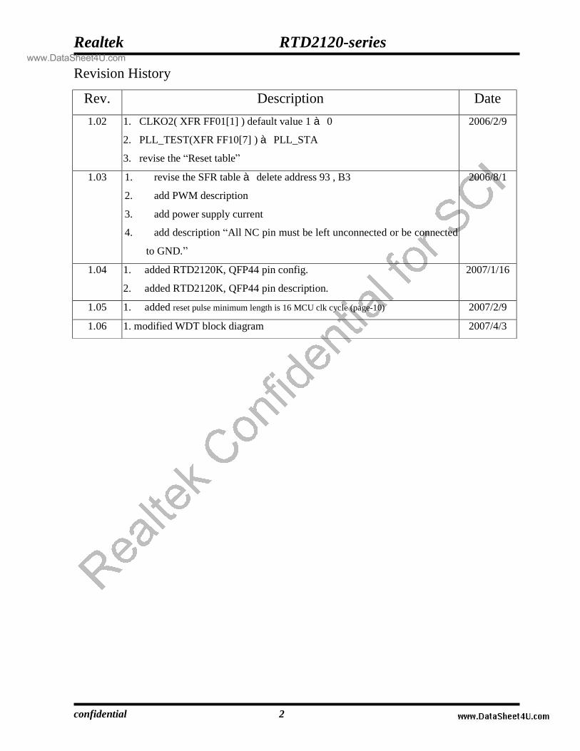
Revision History
Rev. Description Date 1.02 1. CLKO2( XFR FF01[1] ) default value 1 à 0
2. PLL_TEST(XFR FF10[7] ) à PLL_STA
3. revise the “Reset table”
2006/2/9
1.03 1. revise the SFR table à delete address 93 , B3
2. add PWM description
3. add power supply current
4. add description “All NC pin must be left unconnected or be connected
to GND.”
2006/8/1
1.04 1. added RTD2120K, QFP44 pin config.
2. added RTD2120K, QFP44 pin description.
2007/1/16
1.05 1. added reset pulse minimum length is 16 MCU clk cycle (page-10) 2007/2/9
1.06 1. modified WDT block diagram 2007/4/3
www.DataSheet4U.com
Realtek RTD2120-series
confidential 3
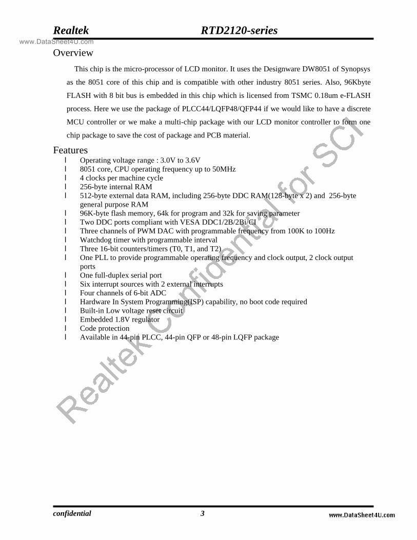
Overview This chip is the micro-processor of LCD monitor. It uses the Designware DW8051 of Synopsys
as the 8051 core of this chip and is compatible with other industry 8051 series. Also, 96Kbyte
FLASH with 8 bit bus is embedded in this chip which is licensed from TSMC 0.18um e-FLASH
process. Here we use the package of PLCC44/LQFP48/QFP44 if we would like to have a discrete
MCU controller or we make a multi-chip package with our LCD monitor controller to form one
chip package to save the cost of package and PCB material.
Features l Operating voltage range : 3.0V to 3.6V l 8051 core, CPU operating frequency up to 50MHz l 4 clocks per machine cycle l 256-byte internal RAM l 512-byte external data RAM, including 256-byte DDC RAM(128-byte x 2) and 256-byte
general purpose RAM l 96K-byte flash memory, 64k for program and 32k for saving parameter l Two DDC ports compliant with VESA DDC1/2B/2Bi/CI l Three channels of PWM DAC with programmable frequency from 100K to 100Hz l Watchdog timer with programmable interval l Three 16-bit counters/timers (T0, T1, and T2) l One PLL to provide programmable operating frequency and clock output, 2 clock output
ports l One full-duplex serial port l Six interrupt sources with 2 external interrupts l Four channels of 6-bit ADC l Hardware In System Programming(ISP) capability, no boot code required l Built-in Low voltage reset circuit l Embedded 1.8V regulator l Code protection l Available in 44-pin PLCC, 44-pin QFP or 48-pin LQFP package
www.DataSheet4U.com
Realtek RTD2120-series
confidential 4
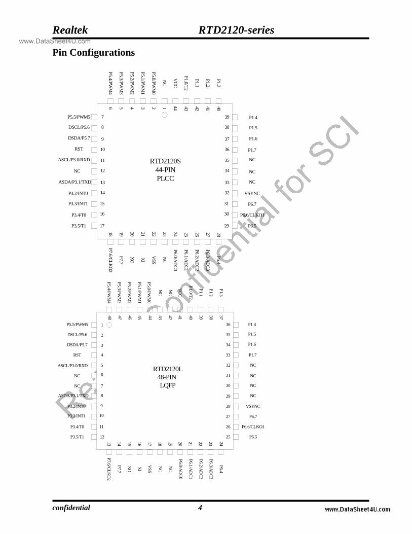
Pin Configurations
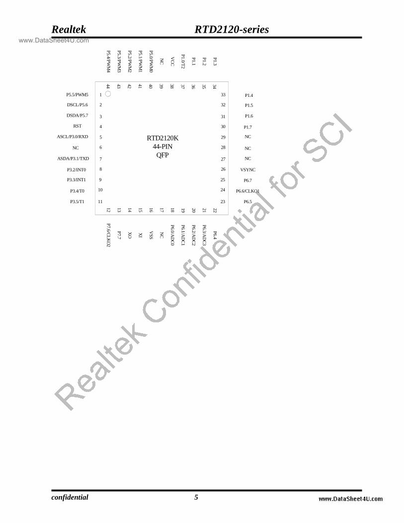
P5.5/PWM5
DSCL/P5.6
DSDA/P5.7
RST
ASCL/P3.0/RXD
ASDA/P3.1/TXD
P3.2/INT0
P3.3/INT1
P3.4/T0
P3.5/T1
P6.4
P1.4
P1.5
P1.6
P1.7
NC
NC
NC
VSYNC
P6.7
P6.6/CLKO1
P6.5
P6.3/A
DC
3
P6.2/A
DC
2
P6.1/A
DC
1
P6.0/A
DC
0
NC
VSS
XI
XO
P7.7
P7.6/C
LK
O2
P1.3
P1.2
P1.0/T
2
VC
C
NC
P5.0/P
WM
0
P5.1/P
WM
1
P5.2/P
WM
2
P5.3/P
WM
3
P5.4/P
WM
4
P1.1
NC
28272625
24232221201918
40414243
44123456
8
7
10
9
12
11
14
13
16
15
17
38
39
36
37
34
35
32
33
30
31
29
RTD2120S44-PINPLCC
2322212019181716151413
38394041434445464748
2
1
4
3
6
5
8
7
10
9
11
35
36
33
34
31
32
29
30
27
28
26
RTD2120L48-PIN LQFP
42 37
12
24
25
P5.5/PWM5
DSCL/P5.6
DSDA/P5.7
RST
ASCL/P3.0/RXD
ASDA/P3.1/TXD
P3.2/INT0
P3.3/INT1
P3.4/T0
P3.5/T1
P6.4
P1.4
P1.5
P1.6
P1.7
NC
NC
NC
VSYNC
P6.7
P6.6/CLKO1
P6.5
P6.3/A
DC
3
P6.2/A
DC
2
P6.1/A
DC
1
P6.0/A
DC
0
NC
VS
S
XI
XO
P7.7
P7.6/C
LK
O2
P1.3
P1.2
P1.0/T
2
VC
C
NC
P5.0/P
WM
0
P5.1/P
WM
1
P5.2/P
WM
2
P5.3/P
WM
3
P5.4/P
WM
4
P1.1
NC
NC
NC
NC
NC
www.DataSheet4U.com
Realtek RTD2120-series
confidential 5
P5.5/PWM5
DSCL/P5.6
DSDA/P5.7
RST
ASCL/P3.0/RXD
ASDA/P3.1/TXD
P3.2/INT0
P3.3/INT1
P3.4/T0
P3.5/T1
P6.4
P1.4
P1.5
P1.6
P1.7
NC
NC
NC
VSYNC
P6.7
P6.6/CLKO1
P6.5P
6.3/AD
C3
P6.2/A
DC
2
P6.1/A
DC
1
P6.0/A
DC
0
NC
VS
S
XI
XO
P7.7
P7.6/C
LK
O2
P1.3
P1.2
P1.0/T
2
VC
C
NC
P5.0/P
WM
0
P5.1/P
WM
1
P5.2/P
WM
2
P5.3/P
WM
3
P5.4/P
WM
4
P1.1
NC
22212019
18171615141312
2
1
4
3
6
5
8
7
10
9
11
32
33
30
31
28
29
26
27
24
25
23
RTD2120K44-PINQFP
34353637
38394041424344
www.DataSheet4U.com
Realtek RTD2120-series
confidential 6
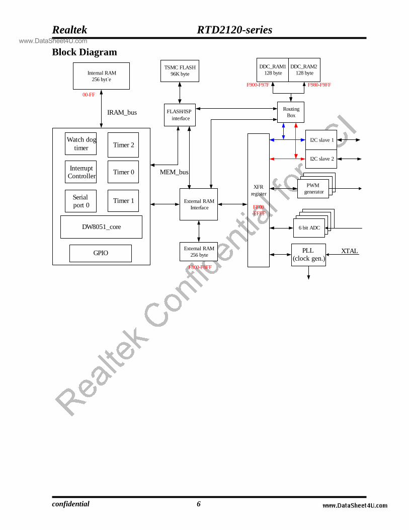
Block Diagram
I2C slave 1
I2C slave 2
6 bit ADC6 bit ADC
6 bit ADC6 bit ADC
PWM
generatorPWM
generatorPWM
generatorXFR
register
FF00-FFFF
TSMC FLASH96K byte
MEM_bus
Internal RAM256 byt`e
IRAM_bus
DW8051_core
DDC_RAM1128 byte
DDC_RAM2128 byte
RoutingBox
FLASH/ISP
interface
Watch dogtimer
InterruptController
PLL (clock gen.)
Timer 2
Timer 0
Timer 1Serial port 0
XTAL
External RAMInterface
External RAM256 byte
F900-F97F F980-F9FF
F800-F8FF
00-FF
GPIO
www.DataSheet4U.com
Realtek RTD2120-series
confidential 7
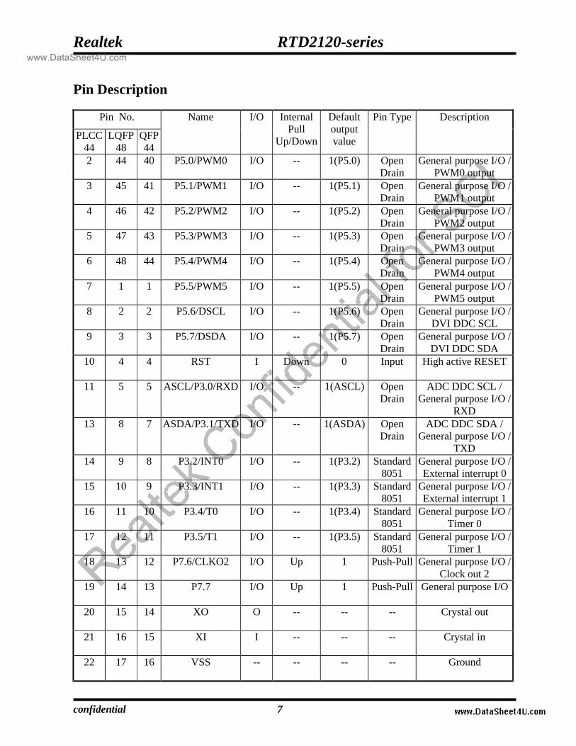
Pin Description
Pin No.
PLCC44
LQFP48
QFP44
Name I/O Internal Pull
Up/Down
Default output value
Pin Type Description
2 44 40 P5.0/PWM0 I/O -- 1(P5.0) Open Drain
General purpose I/O / PWM0 output
3 45 41 P5.1/PWM1 I/O -- 1(P5.1) Open Drain
General purpose I/O / PWM1 output
4 46 42 P5.2/PWM2 I/O -- 1(P5.2) Open Drain
General purpose I/O / PWM2 output
5 47 43 P5.3/PWM3 I/O -- 1(P5.3) Open Drain
General purpose I/O / PWM3 output
6 48 44 P5.4/PWM4 I/O -- 1(P5.4) Open Drain
General purpose I/O / PWM4 output
7 1 1 P5.5/PWM5 I/O -- 1(P5.5) Open Drain
General purpose I/O / PWM5 output
8 2 2 P5.6/DSCL I/O -- 1(P5.6) Open Drain
General purpose I/O / DVI DDC SCL
9 3 3 P5.7/DSDA I/O -- 1(P5.7) Open Drain
General purpose I/O / DVI DDC SDA
10 4 4 RST I Down 0 Input
High active RESET
11 5 5 ASCL/P3.0/RXD I/O -- 1(ASCL) Open Drain
ADC DDC SCL / General purpose I/O /
RXD 13 8 7 ASDA/P3.1/TXD I/O -- 1(ASDA) Open
Drain ADC DDC SDA /
General purpose I/O / TXD
14 9 8 P3.2/INT0 I/O -- 1(P3.2) Standard 8051
General purpose I/O / External interrupt 0
15 10 9 P3.3/INT1 I/O -- 1(P3.3) Standard 8051
General purpose I/O / External interrupt 1
16 11 10 P3.4/T0 I/O -- 1(P3.4) Standard 8051
General purpose I/O / Timer 0
17 12 11 P3.5/T1 I/O -- 1(P3.5) Standard 8051
General purpose I/O / Timer 1
18 13 12 P7.6/CLKO2 I/O Up 1 Push-Pull General purpose I/O / Clock out 2
19 14 13 P7.7 I/O Up 1 Push-Pull
General purpose I/O
20 15 14 XO
O -- -- -- Crystal out
21 16 15 XI
I -- -- -- Crystal in
22 17 16 VSS
-- -- -- -- Ground
www.DataSheet4U.com
Realtek RTD2120-series
confidential 8
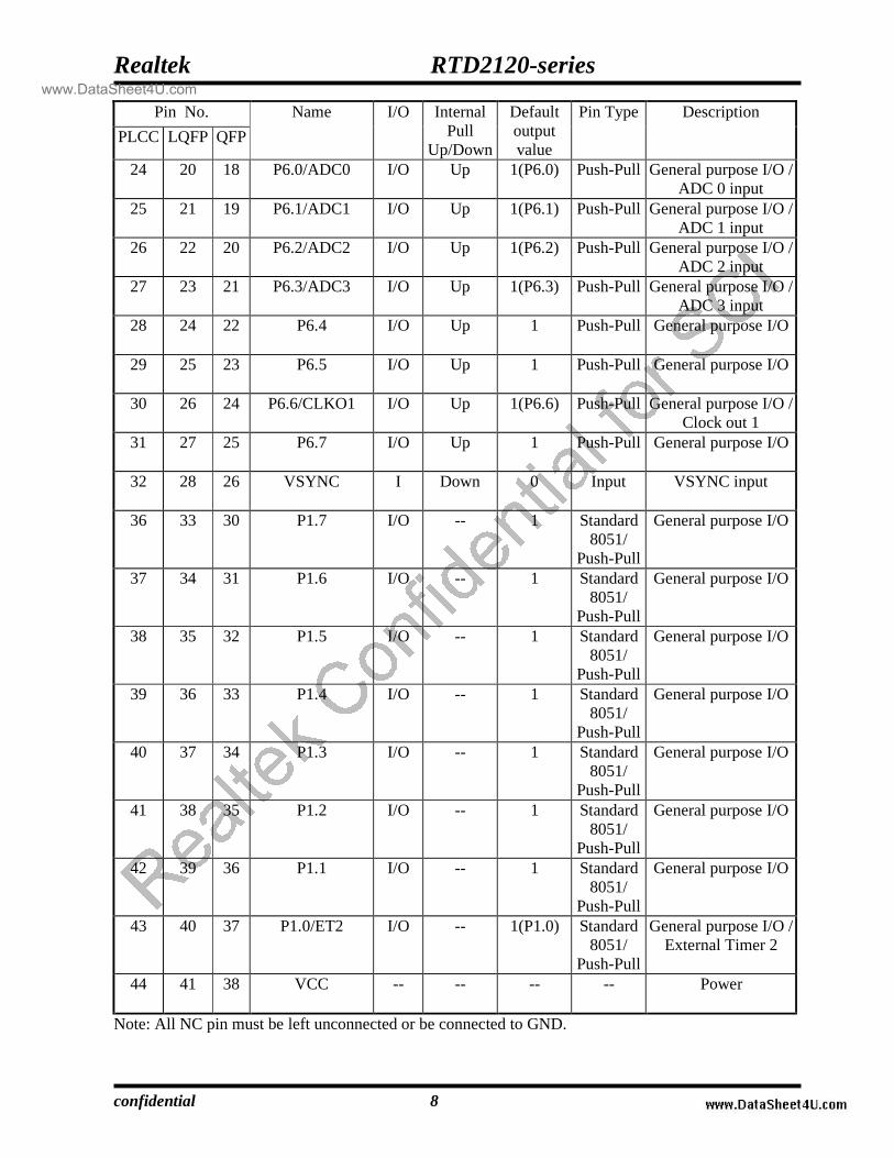
Pin No. PLCC LQFP QFP
Name I/O Internal Pull
Up/Down
Default output value
Pin Type Description
24 20 18 P6.0/ADC0 I/O Up 1(P6.0) Push-Pull General purpose I/O / ADC 0 input
25 21 19 P6.1/ADC1 I/O Up 1(P6.1) Push-Pull General purpose I/O / ADC 1 input
26 22 20 P6.2/ADC2 I/O Up 1(P6.2) Push-Pull General purpose I/O / ADC 2 input
27 23 21 P6.3/ADC3 I/O Up 1(P6.3) Push-Pull General purpose I/O / ADC 3 input
28 24 22 P6.4 I/O Up 1 Push-Pull
General purpose I/O
29 25 23 P6.5 I/O Up 1 Push-Pull
General purpose I/O
30 26 24 P6.6/CLKO1 I/O Up 1(P6.6) Push-Pull
General purpose I/O / Clock out 1
31 27 25 P6.7 I/O Up 1 Push-Pull
General purpose I/O
32 28 26 VSYNC
I Down 0 Input VSYNC input
36 33 30 P1.7 I/O -- 1 Standard 8051/
Push-Pull
General purpose I/O
37 34 31 P1.6 I/O -- 1 Standard 8051/
Push-Pull
General purpose I/O
38 35 32 P1.5 I/O -- 1 Standard 8051/
Push-Pull
General purpose I/O
39 36 33 P1.4 I/O -- 1 Standard 8051/
Push-Pull
General purpose I/O
40 37 34 P1.3 I/O -- 1 Standard 8051/
Push-Pull
General purpose I/O
41 38 35 P1.2 I/O -- 1 Standard 8051/
Push-Pull
General purpose I/O
42 39 36 P1.1 I/O -- 1 Standard 8051/
Push-Pull
General purpose I/O
43 40 37 P1.0/ET2 I/O -- 1(P1.0) Standard 8051/
Push-Pull
General purpose I/O / External Timer 2
44 41 38 VCC
-- -- -- -- Power
Note: All NC pin must be left unconnected or be connected to GND.
www.DataSheet4U.com
Realtek RTD2120-series
confidential 9
DW8051 micro-processor
The DW8051 contained in RTD2120 is compatible with industry standard 803x/805x and provides the following design features and enhancements to the standard 8051 microcontroller: 1. High speed architecture
Compared to standard 8051, the DW8051 processor core provides increased performance by executing instructions in a 4-clock bus cycle, as opposed to the 12-clock bus cycle in the standard 8051. The shortened bus timing improves the instruction execution rate for most instructions by a factor of three over the standard 8051 architectures. The average speed improvement for the entire instruction set is approximately 2.5X. 2. Stretch Memory Cycles
The stretch memory cycle feature enables application software to adjust the speed of data memory access. The DW8051 can execute the MOVX instruction in as little as 2 instruction cycles. However, it is sometimes desirable to stretch this value; for example, to access slow memory or slow memory-mapped peripherals such as UARTs or LCDs.
The three LSBs of the Clock Control Register (at SFR location 8Eh) control the stretch value. You can use stretch values between zero and seven. A stretch value of zero adds zero instruction cycles, resulting in MOVX instructions executing in two instruction cycles. A stretch value of seven adds seven instruction cycles, resulting in MOVX instructions executing in nine instruction cycles. The stretch value can be changed dynamically under program control.
By default, the stretch value resets to one (three cycle MOVX). For full-speed data memory access, the software must set the stretch value to zero. The stretch value affects only data memory access. The only way to reduce the speed of program memory (ROM) access is to use a slower clock. 3. Dual Data Pointers
The DW8051 employs dual data pointers to accelerate data memory block moves. The standard 8051 data pointer (DPTR) is a 16-bit value used to address external data RAM or peripherals. The DW8051 maintains the standard data pointer as DPTR0 at SFR locations 82h and 83h. It is not necessary to modify code to use DPTR0.
The DW8051 adds a second data pointer (DPTR1) at SFR locations 84h and 85h. The SEL bit in the DPTR Select register, DPS (SFR 86h), selects the active pointer. When SEL = 0, instructions that use the DPTR will use DPL0 and DPH0. When SEL = 1, instructions that use the DPTR will use DPL1 and DPH1. SEL is the bit 0 of SFR location 86h. No other bits of SFR location 86h are used.
All DPTR-related instructions use the currently selected data pointer. To switch the active pointer, toggle the SEL bit. The fastest way to do so is to use the increment instruction (INC DPS). This requires only one instruction to switch from a source address to a destination address, saving application code from having to save source and destination addresses when doing a block move.
Using dual data pointers provides significantly increased efficiency when moving large blocks of data.
4. Timer Rate Control
One important difference exists between the RTD2120 and 80C32 regarding timers. The original 80C32 used a 12 clock per cycle scheme for timers and consequently for some serial baud rates(depending on the mode). The RTD2120 architecture normally runs using 4 clocks per cycle. However, in the area of timers, it will default to a 12 clock per cycle scheme on a reset. This allows existing code with real–time dependencies such as baud rates to operate properly. If an application needs higher speed timers or serial baud rates, the timers can be set to run at the 4 clock rate.
www.DataSheet4U.com
Realtek RTD2120-series
confidential 10
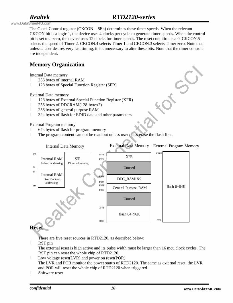
The Clock Control register (CKCON – 8Eh) determines these timer speeds. When the relevant CKCON bit is a logic 1, the device uses 4 clocks per cycle to generate timer speeds. When the control bit is set to a zero, the device uses 12 clocks for timer speeds. The reset condition is a 0. CKCON.5 selects the speed of Timer 2. CKCON.4 selects Timer 1 and CKCON.3 selects Timer zero. Note that unless a user desires very fast timing, it is unnecessary to alter these bits. Note that the timer controls are independent. Memory Organization Internal Data memory l 256 bytes of internal RAM l 128 bytes of Special Function Register (SFR) External Data memory l 128 bytes of External Special Function Register (XFR) l 256 bytes of DDCRAM(128-bytex2) l 256 bytes of general purpose RAM l 32k bytes of flash for EDID data and other parameters External Program memory l 64k bytes of flash for program memory l The program content can not be read out unless user mass erase the flash first.
flash 0~64K
Internal RAMDirect/Indirect
addressing
flash 64~96K
Unused
General Purpose RAM
DDC_RAM1&2
Unused
XFR
0000
7FFF
F800
F8FF
F900
F9FF
FF00
FFFF
Internal RAMIndirect addressing
SFRDirect addressing
Internal Data Memory External Data Memory
0000
FFFF
External Program Memory
00
7F
80
FF
Reset
There are five reset sources in RTD2120, as described below: l RST pin
The external reset is high active and its pulse width must be larger than 16 mcu clock cycles. The RST pin can reset the whole chip of RTD2120.
l Low voltage reset(LVR) and power on reset(POR) The LVR and POR monitor the power status of RTD2120. The same as external reset, the LVR and POR will reset the whole chip of RTD2120 when triggered.
l Software reset
www.DataSheet4U.com
Realtek RTD2120-series
confidential 11
To activate software reset, set FF39[1](SOF_RST). When software reset is triggered, it will reset all modules except debug mode.
l Watchdog timer(WDT) The watchdog timer generates reset when it is overflowed. The watchdog timer resets almost the same modules as software reset except itself(watchdog timer module).
l In System Programing(ISP) reset ISP reset will generate when entering ISP mode. Compared to Watchdog timer reset, ISP mode resets almost the same modules as Watchdog timer except itself(ISP module).
Debug mode module
Watchdog timer module
CPU ISP module and other modules
RST pin O O O O LVR & POR O O O O Software reset x O O O WDT reset x x O x ISP reset x x O x Note: O = Reset , x = No effect Interrupt
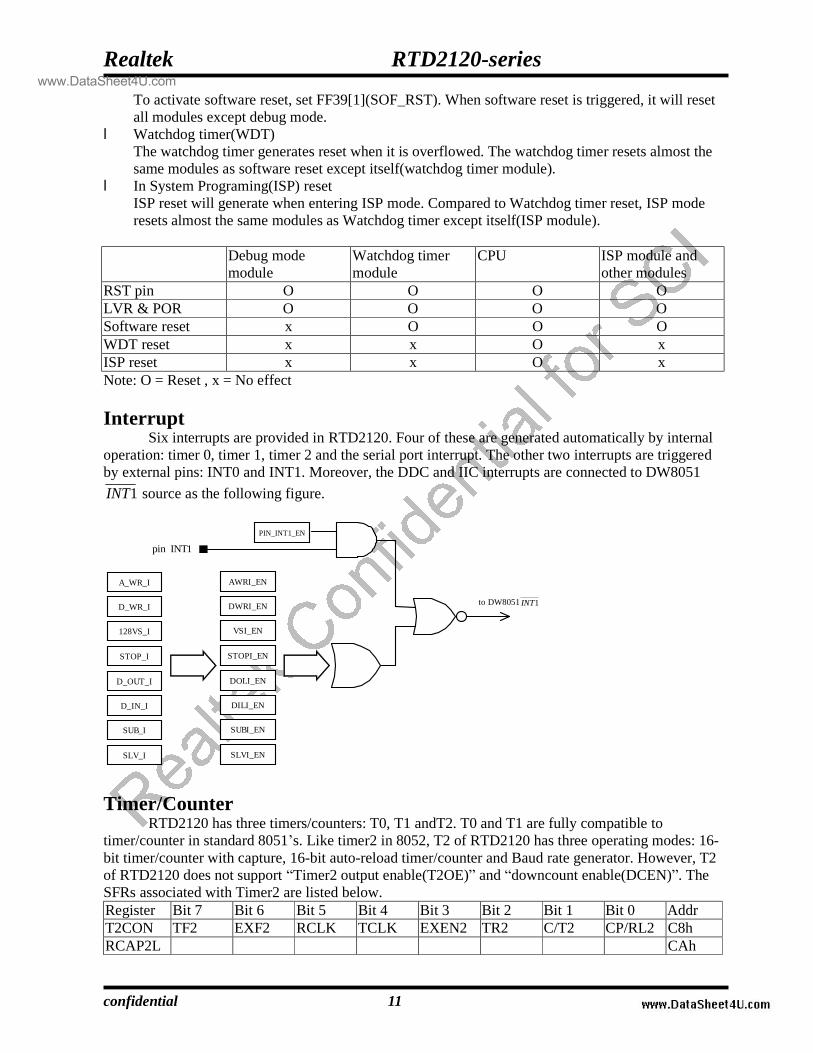
Six interrupts are provided in RTD2120. Four of these are generated automatically by internal operation: timer 0, timer 1, timer 2 and the serial port interrupt. The other two interrupts are triggered by external pins: INT0 and INT1. Moreover, the DDC and IIC interrupts are connected to DW8051
1INT source as the following figure.
A_WR_I AWRI_EN
D_WR_I DWRI_EN
128VS_I VSI_EN
STOP_I STOPI_EN
D_OUT_I DOLI_EN
D_IN_I DILI_EN
SUB_I SUBI_EN
SLV_I SLVI_EN
PIN_INT1_EN
pin INT1
to DW8051 1INT
Timer/Counter
RTD2120 has three timers/counters: T0, T1 andT2. T0 and T1 are fully compatible to timer/counter in standard 8051’s. Like timer2 in 8052, T2 of RTD2120 has three operating modes: 16-bit timer/counter with capture, 16-bit auto-reload timer/counter and Baud rate generator. However, T2 of RTD2120 does not support “Timer2 output enable(T2OE)” and “downcount enable(DCEN)”. The SFRs associated with Timer2 are listed below. Register Bit 7 Bit 6 Bit 5 Bit 4 Bit 3 Bit 2 Bit 1 Bit 0 Addr T2CON TF2 EXF2 RCLK TCLK EXEN2 TR2 C/T2 CP/RL2 C8h RCAP2L CAh
www.DataSheet4U.com
Realtek RTD2120-series
confidential 12
RCAP2H CBh TL2 CCh TH2 CDh 1. 16-bit timer/counter with capture
The Timer 2 capture mode is the same as the 16-bit timer/counter with the addition of the capture registers and control signals. If EXEN2 = 0, Timer2 is a 16-bit timer/counter . The C/T2 bit determines whether the 16-bit counter counts osc cycles (divided by 4 or 12), or high-to-low transitions on the P1.0 pin. The TR2 bit enables the counter. When the count increments from FFFFh, the TF2 flag is set.
The CP/RL2 bit in the T2CON SFR enables the capture feature. When CP/RL2 = 1, a high-to-low transition on P1.1 when EXEN2 = 1 causes the Timer 2 value to be loaded into the capture registers (RCAP2L and RCAP2H).
2. 16-bit timer/counter with auto-reload When CP/RL2 = 0, Timer 2 is configured for the auto-reload mode. Control of counter input is the same as for the other 16-bit counter modes. When the count increments from FFFFh, Timer 2 sets the TF2 flag and the starting value is reloaded into TL2 and TH2. The software must preload the starting value into the RCAP2L and RCAP2H registers. When Timer 2 is in auto-reload mode, a reload can be forced by a high-to-low transition on the P1.1 pin, if enabled by EXEN2 = 1. 3. Baud rate generator Setting either RCLK or TCLK to 1 configures Timer 2 to generate baud rates for Serial Port 0 in serial mode 1 or 3. In baud rate generator mode, Timer 2 functions in auto-reload mode. However, instead of setting the TF2 flag, the counter overflow generates a shift clock for the serial port function. As in normal auto-reload mode, the overflow also causes the preloaded start value in the RCAP2L and RCAP2H registers to be reloaded into the TL2 and TH2 registers. When either TCLK = 1 or RCLK = 1, Timer 2 is forced into auto-reload operation, regardless of the state of the CP/RL2 bit. When operating as a baud rate generator, Timer 2 does not set the TF2 bit. In this mode, a Timer 2 interrupt can only be generated by a high-to-low transition on the P1.1 pin setting the EXF2 bit, and only if enabled by EXEN2 = 1.
The counter time base in baud rate generator mode is osc/2. To use an external clock source, set C/T2 to 1 and apply the desired clock source to the P1.0 pin. Special Function Registers(SFR)
Register
Bit 7
Bit 6
Bit 5
Bit 4
Bit 3
Bit 2
Bit 1
Bit 0
Reset Value (Hex)
Addr (Hex)
SP 07 81 DPL0 00 82 DPH0 00 83 DPL1 00 84 DPH1 00 85 DPS 0 0 0 0 0 0 0 SEL 00 86 PCON SMOD0 1 1 GF1 GF0 STOP IDLE 30 87 TCON TF1 TR1 TF0 TR0 IE1 IT1 IE0 IT0 00 88 TMOD GATE C/T M1 M0 GATE C/T M1 M0 00 89 TL0 00 8A
www.DataSheet4U.com
Realtek RTD2120-series
confidential 13
Register
Bit 7
Bit 6
Bit 5
Bit 4
Bit 3
Bit 2
Bit 1
Bit 0
Reset Value (Hex)
Addr (Hex)
TL1 00 8B TH0 00 8C TH1 00 8D CKCON T2M T1M T0M MD2 MD1 MD0 01 8E SPC_FNC 0 0 0 0 0 0 0 WRS 00 8F P1 P1.7 P1.6 P1.5 P1.4 P1.3 P1.2 P1.1 P1.0 FF 90 MPAGE 00 92 P1_R P1.7 P1.6 P1.5 P1.4 P1.3 P1.2 P1.1 P1.0 FF 93 SCON0 SM0 SM1 SM2 REN TB8 RB8 TI RI 00 98 SBUF0 00 99 P2 P2.7 P2.6 P2.5 P2.4 P2.3 P2.2 P2.1 P2.0 00 A0 IE EA 0 ET2 ES0 ET1 EX1 ET0 EX0 00 A8 P3 P3.7 P3.6 P3.5 P3.4 P3.3 P3.2 P3.1 P3.0 FF B0 P3_R P3.7 P3.6 P3.5 P3.4 P3.3 P3.2 P3.1 P3.0 FF B3 IP 1 0 PT2 PS0 PT1 PX1 PT0 PX0 80 B8 T2CON TF2 EXF2 RCLK TCLK EXEN2 TR2 C/T2 CP/RL2 00 C8 RCAP2L 00 CA RCAP2H 00 CB TL2 00 CC TH2 00 CD PSW CY AC F0 RS1 RS0 OV F1 P 00 D0 ACC 00 E0 B 00 F0 External Special Function Registers(XFR) Pin Share
Register::Pin_share0 0xFF00
Name Bits Read/Write Reset State Comments
Reserved 7 -- 0 Reserved IIC2E 6 R/W 1 0: Pin “P5.6/DSCL“ is P5.6, Pin
“P5.7/DSDA“ is P5.7 1: Pin “P5.6/DSCL“ is DSCL, Pin “P5.7/DSDA“ is DSDA
PWM5E 5 R/W 0 0: Pin “P5.5/PWM5“ is P5.5 1: Pin “P5.5/PWM5“ is PWM5
PWM4E 4 R/W 0 0: Pin “P5.4/PWM4“ is P5.4 1: Pin “P5.4/PWM4“ is PWM4
PWM3E 3 R/W 0 0: Pin “P5.3/PWM3“ is P5.3 1: Pin “P5.3/PWM3“ is PWM3
PWM2E 2 R/W 0 0: Pin “P5.2/PWM2“ is P5.2 1: Pin “P5.2/PWM2“ is PWM2
www.DataSheet4U.com
Realtek RTD2120-series
confidential 14
PWM1E 1 R/W 0 0: Pin “P5.1/PWM1“ is P5.1 1: Pin “P5.1/PWM1“ is PWM1
PWM0E 0 R/W 0 0: Pin “P5.0/PWM0“ is P5.0 1: Pin “P5.0/PWM0“ is PWM0
Register::Pin_share1 0xFF01
Name Bits Read/Write Reset State Comments
A_DDC_PIN_SEL
7 R/W 0 0: ADC DDC ports are connected to ASDA/ASCL 1: ADC DDC ports are connected to DSDA/DSCL
D_DDC_PIN_SEL
6 R/W 1 0: DVI DDC ports are connected to ASDA/ASCL 1: DVI DDC ports are connected to DSDA/DSCL
Reserved 5:3 -- 0 Reserved PIN_INT1_EN
2 R/W 1 Pin “P3.3/INT1” connect to 8051 INT1 enable 0: disable 1: enable when Pin “P3.3/INT1” is used as GPIO, this bit must be 0.
CLKO2E 1 R/W 0 0: Pin “P7.6/CLKO2“ is P7.6 1: Pin “P7.6/CLKO2“ is CLKO2
IIC1E 0 R/W 1 0: Pin “ASCL/P3.0/Rxd“ is P3.0/RXD, Pin “ASDA/P3.1/Txd“ is P3.1/TXD 1: Pin “ASCL/P3.0/Rxd“ is ASCL, Pin “ASDA/P3.1/Txd“ is ASDA
Register::Pin_share2 0xFF02
Name Bits Read/Write Reset State Comments
Reserved 7:5 -- 0 Reserved CLKO1E 4 R/W 0 0: Pin “P6.6/CLKO1“ is P6.6
1: Pin “P6.6/CLKO1“ is CLKO1 ADC3E 3 R/W 0 0: Pin “P6.3/ADC3“ is P6.3
1: Pin “P6.3/ADC3“ is ADC3 ADC2E 2 R/W 0 0: Pin “P6.2/ADC2“ is P6.2
1: Pin “P6.2/ADC2“ is ADC2 ADC1E 1 R/W 0 0: Pin “P6.1/ADC1“ is P6.1
1: Pin “P6.1/ADC1“ is ADC1 ADC0E 0 R/W 0 0: Pin “P6.0/ADC0“ is P6.0
1: Pin “P6.0/ADC0“ is ADC0 I/O port l Each I/O pin of RTD2120 can drive/sink 4mA and the internal pull up/down circuit can
drive/sink 10uA.
www.DataSheet4U.com
Realtek RTD2120-series
confidential 15
l All pins have 5V tolerance except four ADC pins: “P6.0/ADC0”, “P6.1/ADC1”, “P6.2/ADC2” and ”P6.3/ADC3”.
Register::Port5_output_enable 0xFF03
Name Bits Read/Write Reset State Comments
P57OE 7 R/W 0 0: P5.7 is input pin 1: P5.7 is output pin
P56OE 6 R/W 0 0: P5.6 is input pin 1: P5.6 is output pin
P55OE 5 R/W 0 0: P5.5 is input pin 1: P5.5 is output pin
P54OE 4 R/W 0 0: P5.4 is input pin 1: P5.4 is output pin
P53OE 3 R/W 0 0: P5.3 is input pin 1: P5.3 is output pin
P52OE 2 R/W 0 0: P5.2 is input pin 1: P5.2 is output pin
P51OE 1 R/W 0 0: P5.1 is input pin 1: P5.1 is output pin
P50OE 0 R/W 0 0: P5.0 is input pin 1: P5.0 is output pin
Register::Port6_output_enable 0xFF04
Name Bits Read/Write Reset State Comments
P67OE 7 R/W 0 0: P6.7 is input pin 1: P6.7 is output pin
P66OE 6 R/W 0 0: P6.6 is input pin 1: P6.6 is output pin
P65OE 5 R/W 0 0: P6.5 is input pin 1: P6.5 is output pin
P64OE 4 R/W 0 0: P6.4 is input pin 1: P6.4 is output pin
P63OE 3 R/W 0 0: P6.3 is input pin 1: P6.3 is output pin
P62OE 2 R/W 0 0: P6.2 is input pin 1: P6.2 is output pin
P61OE 1 R/W 0 0: P6.1 is input pin 1: P6.1 is output pin
P60OE 0 R/W 0 0: P6.0 is input pin 1: P6.0 is output pin
Register::Port7_output_enable 0xFF05
Name Bits Read/Write Reset State Comments
P77OE 7 R/W 0 0: P7.7 is input pin 1: P7.7 is output pin
www.DataSheet4U.com
Realtek RTD2120-series
confidential 16
P76OE 6 R/W 0 0: P7.6 is input pin 1: P7.6 is output pin
Reserved 5:0 -- 0 Reserved
Register::Port1_pad_type 0xFF09
Name Bits Read/Write Reset State Comments
P17_PPO 7 R/W 0 0:P1.7 is standar 8051 I/O 1:P1.7 is Push-Pull output
P16_PPO 6 R/W 0 0:P1.6 is standar 8051 I/O 1:P1.6 is Push-Pull output
P15_PPO 5 R/W 0 0:P1.5 is standar 8051 I/O 1:P1.5 is Push-Pull output
P14_PPO 4 R/W 0 0:P1.4 is standar 8051 I/O 1:P1.4 is Push-Pull output
P13_PPO 3 R/W 0 0:P1.3 is standar 8051 I/O 1:P1.3 is Push-Pull output
P12_PPO 2 R/W 0 0:P1.2 is standar 8051 I/O 1:P1.2 is Push-Pull output
P11_PPO 1 R/W 0 0:P1.1 is standar 8051 I/O 1:P1.1 is Push-Pull output
P10_PPO 0 R/W 0 0:P1.0 is standar 8051 I/O 1:P1.0 is Push-Pull output
Register::Port50_pin_reg 0xFF50
Name Bits Read/Write Reset State Comments
Reserved 7:1 -- 0 Reserved P50 0 R/W 1 Input/output value of P5.0
Register::Port51_pin_reg 0xFF51
Name Bits Read/Write Reset State Comments
Reserved 7:1 -- 0 Reserved P51 0 R/W 1 Input/output value of P5.1
Register::Port52_pin_reg 0xFF52
Name Bits Read/Write Reset State Comments
Reserved 7:1 -- 0 Reserved P52 0 R/W 1 Input/output value of P5.2
www.DataSheet4U.com
Realtek RTD2120-series
confidential 17
Register::Port53_pin_reg 0xFF53
Name Bits Read/Write Reset State Comments
Reserved 7:1 -- 0 Reserved P53 0 R/W 1 Input/output value of P5.3
Register::Port54_pin_reg 0xFF54
Name Bits Read/Write Reset State Comments
Reserved 7:1 -- 0 Reserved P54 0 R/W 1 Input/output value of P5.4
Register::Port55_pin_reg 0xFF55
Name Bits Read/Write Reset State Comments
Reserved 7:1 -- 0 Reserved P55 0 R/W 1 Input/output value of P5.5
Register::Port56_pin_reg 0xFF56
Name Bits Read/Write Reset State Comments
Reserved 7:1 -- 0 Reserved P56 0 R/W 1 Input/output value of P5.6
Register::Port57_pin_reg 0xFF57
Name Bits Read/Write Reset State Comments
Reserved 7:1 -- 0 Reserved P57 0 R/W 1 Input/output value of P5.7
Register::Port60_pin_reg 0xFF58
Name Bits Read/Write Reset State Comments
Reserved 7:1 -- 0 Reserved P60 0 R/W 1 Input/output value of P6.0
www.DataSheet4U.com

Realtek RTD2120-series
confidential 18
Register::Port61_pin_reg 0xFF59
Name Bits Read/Write Reset State Comments
Reserved 7:1 -- 0 Reserved P61 0 R/W 1 Input/output value of P6.1
Register::Port62_pin_reg 0xFF5A
Name Bits Read/Write Reset State Comments
Reserved 7:1 -- 0 Reserved P62 0 R/W 1 Input/output value of P6.2
Register::Port63_pin_reg 0xFF5B
Name Bits Read/Write Reset State Comments
Reserved 7:1 -- 0 Reserved P63 0 R/W 1 Input/output value of P6.3
Register::Port64_pin_reg 0xFF5C
Name Bits Read/Write Reset State Comments
Reserved 7:1 -- 0 Reserved P64 0 R/W 1 Input/output value of P6.4
Register::Port65_pin_reg 0xFF5D
Name Bits Read/Write Reset State Comments
Reserved 7:1 -- 0 Reserved P65 0 R/W 1 Input/output value of P6.5
Register::Port66_pin_reg 0xFF5E
Name Bits Read/Write Reset State Comments
Reserved 7:1 -- 0 Reserved P66 0 R/W 1 Input/output value of P6.6
www.DataSheet4U.com
Realtek RTD2120-series
confidential 19
Register::Port67_pin_reg 0xFF5F
Name Bits Read/Write Reset State Comments
Reserved 7:1 -- 0 Reserved P67 0 R/W 1 Input/output value of P6.7
Register::Port76_pin_reg 0xFF60
Name Bits Read/Write Reset State Comments
Reserved 7:1 -- 0 Reserved P76 0 R/W 1 Input/output value of P7.6
Register::Port77_pin_reg 0xFF61
Name Bits Read/Write Reset State Comments
Reserved 7:1 -- 0 Reserved P77 0 R/W 1 Input/output value of P7.7
Low Voltage Reset & Power on Reset When the voltage level of power supply is below VLT, the low voltage reset(LVR) generates a chip reset signal. After the power supply is above VUT(2.6V), LVR remain in reset state for 65536 X’tal cycle(tPOR) to guarantee the chip exit reset condition.
VUT
VLT
tPOR
VCC
VSS
INTERNAL RESET
Register::LVR_control 0xFF0A
Name Bits Read/Write Reset State Comments
www.DataSheet4U.com
Realtek RTD2120-series
confidential 20
VLT 7:6 R/W 0 low_threshold_voltage 00:1.8V 01:2.0V 10:2.2V 11:2.4V
reserved 5:0 -- 00 reserved A/D Converter
RTD2120 has embedded 4 channels of analog-to-digital converter. The ADCs convert analog input voltage on the four A/D input pins to four 6-bit digital data stored in XFRs (FF0C~FF0F) sequentially. The ADC conversion range is from GND to VDD and the conversion is linear and monotonic with no missing codes. To start A/D conversion, set STRT_ADC(FF0B[7]) = 1 and the conversion will be complete in less than 12 us for 4 channels.
Register::ADC_control 0xFF0B
Name Bits Read/Write Reset State Comments
STRT_ADC 7 R/W 0 Write 1 to start the A/D conversion. Auto clear when A/D Conversion has been completed. 0:A/D Conversion has been completed 1:A/D Conversion is not completed yet
ADC_TEST 6 R/W 0 0: Normal operation 1: ADC test mode
reserved 5:3 R/W 0 Reserved BIAS_ADJ 2:1 R/W 1 ADC bias current adjust
00: 15u 01: 20u 10: 25u 11: 30u
CK_SEL 0 R/W 0 Inverse ADC input clock pos/neg 0: pos 1: neg
Register::ADC0_convert_result 0xFF0C
Name Bits Read/Write Reset State Comments
ADC0_CONV_DATA
7:2 R 3F Converted data of ADC0
reserved 1:0 -- 00
Register::ADC1_convert_result 0xFF0D
www.DataSheet4U.com
Realtek RTD2120-series
confidential 21
Name Bits Read/Write Reset State Comments
ADC1_CONV_DATA
7:2 R 3F Converted data of ADC1
reserved 1:0 -- 00
Register::ADC2_convert_result 0xFF0E
Name Bits Read/Write Reset State Comments
ADC2_CONV_DATA
7:2 R 3F Converted data of ADC2
reserved 1:0 -- 00
Register::ADC3_convert_result 0xFF0F
Name Bits Read/Write Reset State Comments
ADC3_CONV_DATA
7:2 R 3F Converted data of ADC3
reserved 1:0 -- 00 PLL
RTD2120 contains a PLL to make the whole chip operate at higher or lower speed for different demands. After reset, RTD2120 uses crystal frequency as the system clock. User can program the PLL to operate at the desired frequency and select system clock to PLL output by setting MCU_CLK_SEL. RTD2120 will switch system clock to PLL output only when PLL is stable. Moreover, the divider is glitch free so user can modify its value at any time.For normal operation, user must choose the crystal whose frequency is between 11M and 27MHz . Besides, VCO frequency must be programmed between 40M and 80MHz. Note: Fvco = Xtal *(M/N) , where M=M_code+1, N=N_code+1.
Crystal
11M~27MHzN
DIV
PFD VCO
M
40M~80MHz
PUMP
MCU_CLK_SEL
MCU_CLK
www.DataSheet4U.com
Realtek RTD2120-series
confidential 22
Register::PLL_control 0xFF10
Name Bits Read/Write Reset State Comments
PLL_STA 7 R 1 PLL status 0: normal operation 1: PLL abnormal or PLL power down
DVSET 6:5 R/W 2 Test mode vctrl set 11(0.8v) 10(1.0v) 01(1.2v) 00(1.4v)
reserved 4:3 -- 0 WD_RST 2 R/W 0 0: No effect
1: Watchdog reset WD_SET 1 R/W 0 0: No effect
1: Watchdog set PWDN_PLL 0 R/W 1 0: normal operation
1: power down PLL
Register::PLL_filter_control 0xFF11
Name Bits Read/Write Reset State Comments
reserved 7:4 -- 0 VR
3:2 R/W 0 Loop filter resister 00: 16.32k 01: 19.12k 10: 21.92k 11: 24.72k
PLL_IP 1:0 R/W 2 Charge Pump current Ich=5u+bit[1]*10u+ bit[0]*5u
Register::PLL_M_N_DIV 0xFF12
Name Bits Read/Write Reset State Comments
M_CODE 7:4 R/W 1 Actual M = M_CODE+1 N_CODE 3:2 R/W 0 Actual N = N_CODE+1 DIV 1:0 R/W 0 Divider value
00:1 01:1/2 10:1/4 11:1/8
3.3V to 1.8V Regulator
max typ min
Input voltage(V) 2
Output current(mA) 80
www.DataSheet4U.com
Realtek RTD2120-series
confidential 23
Register::regulator_control 0xFF13
Name Bits Read/Write Reset State Comments
reserved 7:5 -- 0 VBG 4:3 R/W 1 bandgap voltage select
00: 1.14v 01: 1.20v 10: 1.27v 11: 1.34v
V_SEL 2:0 R/W 4 Regulator 1.8v voltage select 000: 2.22 001: 2.12 010: 2.0 011: 1.9 100: 1.8 101: 1.7 110: 1.6 111: 1.5
DDC
RTD2120 has two DDC ports for both D-sub and DVI interface. The external master can access DDC_RAM1(F900~F97F) through pin ASDL and ASDA by ADC DDC channel or DDC_RAM2 (F980~F9FF) through pin DSDL and DSDA by DVI DDC channel. Besides, the DDC_RAM1 and DDC_RAM2 can be combined together to form a 256-bytes DDC_RAM for just ADC/DVI DDC slave by setting DDCRAM_SIZ (FF26[1:0]).
The DDC of RTD2120 is compliant with VESA DDC standard. Both DDC slaves are in DDC1 mode after reset. When a high to low transition is detected on ASCL/DSCL pin, the DDC slave will enter DDC2 transition mode. The DDC slave can revert to DDC1 mode if the SCL signal keeps unchanged for 128 VSYNC periods in DDC2 transition mode and RVT_A_DDC1_EN / RVT_D_DDC1_EN = 1. In DDC2 transition mode, the DDC slave will lock in DDC2 mode if a valid control byte is received. Furthermore, user can force the DDC slave to operate DDC2 mode by setting A_DDC2 / D_DDC2 = 1. (Refers to the VESA “Display Data Channel Standard” for detailed)
Register::ADC_DDC_enable 0xFF20
Name Bits Read/Write Reset State Comments
A_DDC_ADDR
7:5 R/W 0 ADC DDC Channel Address Least Significant 3 Bits (The default DDC channel address MSB 4 Bits is “A”)
reserved 4 -- 0 Reserved A_DDC_W_STA
3 R/W 0 ADC DDC Write Status (for external DDC access only) It is cleared after write.
A_DDCRAM_W_EN
2 R/W 0 ADC DDC SRAM Write Enable (for external DDC access only)
www.DataSheet4U.com
Realtek RTD2120-series
confidential 24
0: Disable 1: Enable
A_DBN_EN 1 R/W 1 ADC DDC De-bounce Enable 0: Disable 1: Enable (with crystal/4)
A_DDC_EN 0 R/W 0 ADC DDC Channel Enable Bit 0: MCU access Enable 1: DDC channel Enable
Register::ADC_DDC_control 0xFF21
Name Bits Read/Write Reset State Comments
A_DBN_CLK_SEL
7:6 R/W 0 De-bounce clock divider 00: 1/1 reference clock 01: 1/2 reference clock 1X: 1/4 reference clock
A_STOP_DBN_SEL
5:4 R/W 0 De-bounce sda stage 0X: latch one stage 10: latch two stage 11: latch three stage
A_SYS_CK_SEL
3 R/W 0 De-bounce reference clock 0: crystal clock 1: PLL clock
A_DDC2 2 R/W 0 Force to ADC DDC to DDC2 mode 0: Normal operation 1: DDC2 is active
RST_A_DDC 1 R/W 0 Reset ADC DDC circuit 0: Normal operation 1: reset (auto cleared)
RVT_A_DDC1_EN
0 R/W 0 ADC DDC revert to DDC1 enable(SCL idle for 128 VSYNC) 0: Disable 1: Enable
Register::DVI_DDC_enable 0xFF23
Name Bits Read/Write Reset State Comments
D_DDC_ADDR
7:5 R/W 0 DVI DDC Channel Address Least Significant 3 Bits (The default DDC channel address MSB 4 Bits is “A”)
reserved 4 -- 0 Reserved D_DDC_W_STA
3 R/W 0 DVI DDC External Write Status (for external DDC access only) It is cleared after write.
D_DDCRAM_W_EN
2 R/W 0 DVI DDC External Write Enable (for external DDC access only) 0: Disable 1: Enable
D_DBN_EN 1 R/W 1 DVI DDC Debounce Enable 0: Disable 1: Enable (with crystal/4)
www.DataSheet4U.com
Realtek RTD2120-series
confidential 25
D_DDC_EN 0 R/W 0 DVI DDC Channel Enable Switch 0: MCU access Enable 1: External DDC access Enable
Register::DVI_DDC_control 0xFF24
Name Bits Read/Write Reset State Comments
D_DBN_CLK_SEL
7:6 R/W 0 De-bounce clock divider 00: 1/1 reference clock 01: 1/2 reference clock 1X: 1/4 reference clock
D_STOP_DBN_SEL
5:4 R/W 0 De-bounce sda stage 0X: latch one stage 10: latch two stage 11: latch three stage
D_SYS_CK_SEL
3 R/W 0 De-bounce reference clock 0: crystal clock 1: PLL clock
D_DDC2 2 R/W 0 Force to DVI DDC to DDC2 mode 0: Normal operation 1: DDC2 is active
RST_D_DDC 1 R/W 0 Reset DVI DDC circuit 0: Normal operation 1: reset (auto cleared)
RVT_D_DDC1_EN
0 R/W 0 DVI DDC revert to DDC1 enable(SCL idle for 128 VSYNC) 0: Disable 1: Enable
Register::DDCRAM_partition 0xFF26
Name Bits Read/Write Reset State Comments
reserved 7:3 -- 00 Reserved VS_CON 2 R/W 0 0: VSYNC signal is connected to ADC DDC
1: VSYNC signal is connected to DVI DDC DDCRAM_SIZ
1:0 R/W 0 0x:ADC DDCRAM=128 byte, DVI DDCRAM=128 byte 10:ADC DDCRAM=0 byte, DVI DDCRAM=256 byte 11:ADC DDCRAM=256 byte, DVI DDCRAM=0 byte
IIC Interface
Register::IIC_set_slave 0xFF27
www.DataSheet4U.com
Realtek RTD2120-series
confidential 26
Name Bits Read/Write Reset State Comments
IIC_ADDR 7:1 R/W 37 IIC Slave Address to decode CH_SEL 0 R/W 0 Channel Select
0: from ADC DDC 1: from DVI DDC
Register::IIC_sub_in 0xFF28
Name Bits Read/Write Reset State Comments
IIC_SUB_ADDR
7:0 R 00 IIC Sub-Address Received
Register::IIC_data_in 0xFF29
Name Bits Read/Write Reset State Comments
IIC_D_IN 7:0 R 00 IIC data received
Register::IIC_data_out 0xFF2A
Name Bits Read/Write Reset State Comments
IIC_D_OUT 7:0 W 00 IIC data to be transmitted
Register::IIC_status 0xFF2B
Name Bits Read/Write Reset State Comments
A_WR_I 7 R/W 0 If ADC DDC detects a STOP condition in write mode, this bit is set to “1” . Write 0 to clear.
D_WR_I 6 R/W 0 If DVI DDC detects a STOP condition in write mode, this bit is set to “1” . Write 0 to clear.
128VS_I 5 R/W 0 In DDC2 Transition mode, SCL idle for 128 VSYNC. Write 0 to clear.
STOP_I 4 R/W 0 If IIC detects a STOP condition(slave address must match), this bit is set to “1” . Write 0 to clear.
D_OUT_I 3 R 0 If IIC_DATA_OUT loaded to serial-out-byte, this bit is set to “1”. Write IIC_data_out (FF2A) to clear.
D_IN_I 2 R 0 If IIC_DATA_IN latched, this bit is set to “1” . Read IIC_data_in (FF29) to clear.
SUB_I 1 R/W 0 If IIC_SUB latched, this bit is set to “1” Write 0 to clear.
www.DataSheet4U.com
Realtek RTD2120-series
confidential 27
SLV_I 0 R/W 0 If IIC_SLAVE latched, this bit is set to “1” Write 0 to clear.
Register::IIC_IRQ_control 0xFF2C
Name Bits Read/Write Reset State Comments
AWI_EN 7 R/W 0 0: Disable the A_WR_I signal as an interrupt source 1: Enable the A_WR_I signal as an interrupt source
DWI_EN 6 R/W 0 0: Disable the D_WR_I signal as an interrupt source 1: Enable the D_WR_I signal as an interrupt source
128VSI_EN 5 R/W 0 0: Disable the 128VS_I signal as an interrupt source 1: Enable the 128VS_I signal as an interrupt source
STOPI_EN 4 R/W 0 0: Disable the STOP_I signal as an interrupt source 1: Enable the STOP_I signal as an interrupt source
DOI_EN 3 R/W 0 0: Disable the D_OUT_I signal as an interrupt source 1: Enable the D_OUT_I signal as an interrupt source
DII_EN 2 R/W 0 0: Disable the D_IN_I signal as an interrupt source 1: Enable the D_IN_I signal as an interrupt source
SUBI_EN 1 R/W 0 0: Disable the SUB_I signal as an interrupt source 1: Enable the SUB_I signal as an interrupt source
SLVI_EN 0 R/W 0 0: Disable the SLV_I signal as an interrupt source 1: Enable the SLV_I signal as an interrupt source
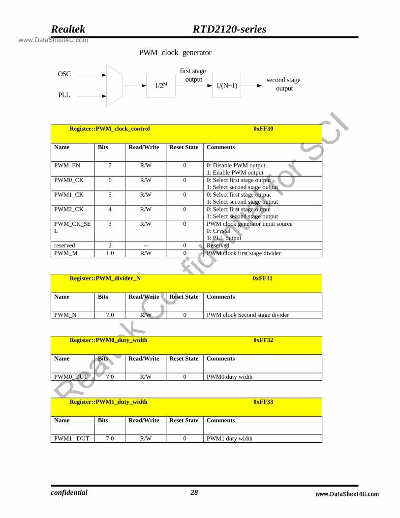
PWM RTD2120 supports 3 channels of PWM DAC. The resolution of each PWM is 8-bit. PWM0, PWM1and PWM2 are connected to DA0, DA1and DA2 respectively. Meanwhile, they can also be connected to DA3, DA4 and DA5 which are programed via PWM_source_select register. The figure below represent the PWM clock generator. Based on the clock, we make up the PWM waveform which frequency is 1/256 of the PWM clock.
www.DataSheet4U.com
Realtek RTD2120-series
confidential 28
1/2M 1/(N+1)
OSC
PLL
PWM clock generator
first stage output second stage
output
Register::PWM_clock_control 0xFF30
Name Bits Read/Write Reset State Comments
PWM_EN 7 R/W 0 0: Disable PWM output 1: Enable PWM output
PWM0_CK 6 R/W 0 0: Select first stage output 1: Select second stage output
PWM1_CK 5 R/W 0 0: Select first stage output 1: Select second stage output
PWM2_CK 4 R/W 0 0: Select first stage output 1: Select second stage output
PWM_CK_SEL
3 R/W 0 PWM clock generator input source 0: Crystal 1: PLL output
reserved 2 -- 0 Reserved PWM_M 1:0 R/W 0 PWM clock first stage divider
Register::PWM_divider_N 0xFF31
Name Bits Read/Write Reset State Comments
PWM_N 7:0 R/W 0 PWM clock Second stage divider
Register::PWM0_duty_width 0xFF32
Name Bits Read/Write Reset State Comments
PWM0_DUT 7:0 R/W 0 PWM0 duty width
Register::PWM1_duty_width 0xFF33
Name Bits Read/Write Reset State Comments
PWM1_ DUT 7:0 R/W 0 PWM1 duty width
www.DataSheet4U.com
Realtek RTD2120-series
confidential 29
Register::PWM2_duty_width 0xFF34
Name Bits Read/Write Reset State Comments
PWM2_ DUT 7:0 R/W 0 PWM2 duty width
Register::PWM_source_select 0xFF35
Name Bits Read/Write Reset State Comments
reserved 7:6 -- 0 Reserved PWM5_SEL 5:4 R/W 2 00: PWM5 is the same as PWM0
01: PWM5 is the same as PWM1 1x: PWM5 is the same as PWM2
PWM4_SEL 3:2 R/W 1 00: PWM4 is the same as PWM0 01: PWM4 is the same as PWM1 1x: PWM4 is the same as PWM2
PWM3_SEL 1:0 R/W 0 00: PWM3 is the same as PWM0 01: PWM3 is the same as PWM1 1x: PWM3 is the same as PWM2
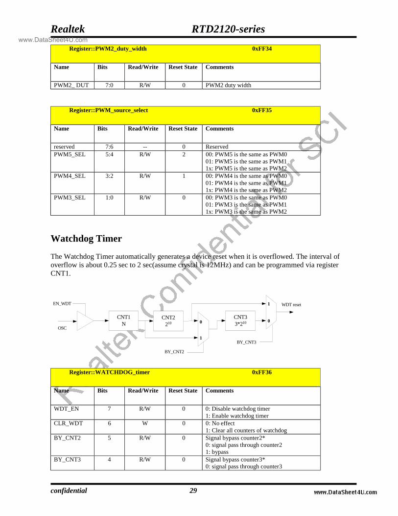
Watchdog Timer The Watchdog Timer automatically generates a device reset when it is overflowed. The interval of overflow is about 0.25 sec to 2 sec(assume crystal is 12MHz) and can be programmed via register CNT1.
CNT1N
EN_WDT
BY_CNT3
WDT reset
OSC
0 0
1
1
CNT33*210
CNT2210
BY_CNT2
Register::WATCHDOG_timer 0xFF36
Name Bits Read/Write Reset State Comments
WDT_EN 7 R/W 0 0: Disable watchdog timer 1: Enable watchdog timer
CLR_WDT 6 W 0 0: No effect 1: Clear all counters of watchdog
BY_CNT2 5 R/W 0 Signal bypass counter2* 0: signal pass through counter2 1: bypass
BY_CNT3 4 R/W 0 Signal bypass counter3* 0: signal pass through counter3
www.DataSheet4U.com
Realtek RTD2120-series
confidential 30
1: bypass reserved 3 -- 0 Reserved CNT1 2:0 R/W 0 The number N of counter1
000~111: 1~8 l When ISP mode is enabled, watchdog will be disabled by hardware. *When BY_CNT2 and BY_CNT3 are all assigned one (bypass), watchdog will be counted by CNT2 In System Programming
User can program the embedded 96K flash of RTD2120 by internal hardware without removing RTD2120 from the system. RTD2120 utilizes DDC channel (ADC/DVI DDC) to communicate with IIC host for ISP function. The ISP protocol is mainly compatible with DDC protocol. However, one significant difference is that the LSB of 7-bit ISP address is the address auto increase bit. Thus, we can improve the flash program speed.
Register::ISP_slave_address 0xFF37
Name Bits Read/Write Reset State Comments
ISP_ADDR 7:2 R/W 25 ISP slave address ISP_ADDR_INC_A
1 R 1 Received LSB of ISP slave address of ADC DDC channel 0: address is nonincrease 1: address is auto-increase
ISP_ADDR_INC_D
0 R 1 Received LSB of ISP slave address of DVI DDC channel 0: address is nonincrease 1: address is auto-increase
Register::option 0xFF38
Name Bits Read/Write Reset State Comments
PORT_PIN_REG
7 R/W 1 port_pin_reg_n enable 0: port_pin_reg_n signal is disabled 1: port_pin_reg_n signal is enabled
reserved 6:2 -- 0 Reserved MCU_CLK_SEL
1 R/W 0 CPU clock source select 0: CPU clock is from Crystal divided by DIV 1: CPU clock is from PLL divided by DIV
CKOUT_SEL 0 R/W 0 CLKO1 & CLKO2 select 0: Select Crystal output 1: Select PLL output
Register::flash_page_erase_control 0xFF39
Name Bits Read/Write Reset State Comments
www.DataSheet4U.com
Realtek RTD2120-series
confidential 31
PAGE_ADDR 7:3 R/W 00 Flash page address from 64K to 96K reserved 2 -- 0 Reserved SOF_RST 1 R/W 0 Software reset for debug mode
0: No effect 1: reset RTD2120
STR_P_ERS 0 R/W 0 Start page erase 0: page erase complete 1: write 1 to start page erase
Register::RAM_test 0xFF3A
Name Bits Read/Write Reset State Comments
reserved 7:4 -- 0 Reserved EXT_RAM_BIST
3 R/W 0 Start BIST function for MCU external RAM (512 bytes)
0: finished and clear 1: start
EXT_RAM_STA
2 R 0 Test result about MCU external RAM 0: fail 1: ok
INT_RAM_BIST
1 R/W 0 Start BIST function for MCU internal RAM (256 bytes)
0: finished and clear 1: start
INT_RAM_STA
0 R 0 Test result about MCU internal RAM 0: fail 1: ok
www.DataSheet4U.com
Realtek RTD2120-series
confidential 32
Memory map of XFR
Register name Addr Bit7 Bit6 Bit5 Bit4 Bit3 Bit2 Bit1 Bit0
Pin_share0 FF00 IIC2E PWM5E PWM4E PWM3E PWM2E PWM1E PWM0E
Pin_share1 FF01 A_DDC_PIN_SEL
D_DDC_PIN_SEL PIN_INT1
_EN CLKO2E IIC1E
Pin_share2 FF02 CLKO1E ADC3E ADC2E ADC1E ADC0E Port5_output_enabl
e FF03 P57OE P56OE P55OE P54OE P53OE P52OE P51OE P50OE Port6_output_enabl
e FF04 P67OE P66OE P65OE P64OE P63OE P62OE P61OE P60OE Port7_output_enabl
e FF05 P77OE P76OE
Port1_pad_type FF09 P17_PPO P16_PPO P15_PPO P14_PPO P13_PPO P12_PPO P11_PPO P10_PPO
LVR_control FF0A VLT
ADC_control FF0B STRT_ADC
ADC_TEST BIAS_ADJ CK_SEL
ADC0_convert_result FF0C ADC0_CONV_DATA
ADC1_convert_result FF0D ADC1_CONV_DATA
ADC2_convert_result FF0E ADC2_CONV_DATA
ADC3_convert_result FF0F ADC3_CONV_DATA
PLL_control FF10 PLL_STA DVSET WD_RST WD_SET PWDN_PLL
PLL_filter_control FF11 VR PLL_IP
PLL_M_N_DIV FF12 M_CODE N_CODE DIV
Regulator_control FF13 VBG V_SEL
ADC_DDC_enable FF20 A_DDC_ADDR A_DDC_W_STA
A_DDCRAM_W_E
N
A_DBN_EN
A_DDC_EN
ADC_DDC_control FF21 A_DBN_CLK_SEL A_STOP_DBN_SEL A_SYS_C
K_SEL A_DDC2 RST_A_DDC
RVT_A_DDC1_EN
DVI_DDC_enable FF23 D_DDC_ADDR D_DDC_W_STA
D_DDCRAM_W_E
N
D_DBN_EN
D_DDC_EN
DVI_DDC_control FF24 D_DBN_CLK_SEL D_STOP_DBN_SEL D_SYS_CK_SEL D_DDC2 RST_D_D
DC RVT_D_DDC1_EN
DDCRAM_partition FF26 VS_CON DDCRAM_SIZ
IIC_set_slave FF27 IIC_ADDR CH_SEL
IIC_sub_in FF28 IIC_SUB_ADDR
IIC_data_in FF29 IIC_D_IN
IIC_data_out FF2A IIC_D_OUT
www.DataSheet4U.com
Realtek RTD2120-series
confidential 33
Register name Addr Bit7 Bit6 Bit5 Bit4 Bit3 Bit2 Bit1 Bit0
IIC_status FF2B A_WR_I D_WR_I 128VS_I STOP_I D_OUT_I D_IN_I SUB_I SLV_I
IIC_IRQ_control FF2C AWI_EN DWI_EN 128VSI_EN
STOPI_EN DOI_EN DII_EN SUBI_EN SLVI_EN
PWM_clock_control FF30 PWM_EN PWM0_C
K PWM1_C
K PWM2_C
K PWM_CK
_SEL PWM_M
PWM_divider_N FF31 PWM_N
PWM0_duty_width FF32 PWM0_DUT
PWM1_duty_width FF33 PWM1_DUT
PWM2_duty_width FF34 PWM2_DUT
PWM_source_select FF35 PWM5_SEL PWM4_SEL PWM3_SEL
WATCHDOG_timer FF36 WDT_EN CLR_WD
T BY_CNT2 BY_CNT3 CNT1
ISP_slave_address FF37 ISP_ADDR ISP_ADDR_INC_A
ISP_ADDR_INC_D
option FF38 PORT_PIN_REG MCU_CL
K_SEL CKOUT_
SEL Flash_page_erase_
control FF39 PAGE_ADDR SOF_RST STR_P_ERS
RAM_test FF3A EXT_RAM_BIST
EXT_RAM_STA
INT_RAM_BIST
INT_RAM_STA
www.DataSheet4U.com
Realtek RTD2120-series
confidential 34
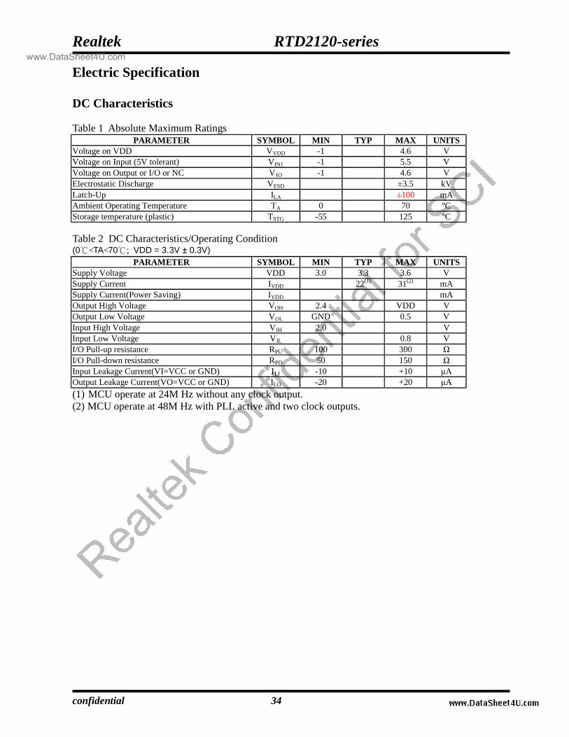
Electric Specification DC Characteristics Table 1 Absolute Maximum Ratings
PARAMETER SYMBOL MIN TYP MAX UNITS Voltage on VDD VVDD -1 4.6 V Voltage on Input (5V tolerant) VIN1 -1 5.5 V Voltage on Output or I/O or NC V IO -1 4.6 V Electrostatic Discharge VESD ±3.5 kV Latch-Up ILA ±100 mA Ambient Operating Temperature TA 0 70 ºC Storage temperature (plastic) TSTG -55 125 ºC Table 2 DC Characteristics/Operating Condition (0℃<TA<70℃; VDD = 3.3V ± 0.3V)
PARAMETER SYMBOL MIN TYP MAX UNITS Supply Voltage VDD 3.0 3.3 3.6 V Supply Current IVDD 22(1) 31(2) mA Supply Current(Power Saving) IVDD mA Output High Voltage VOH 2.4 VDD V Output Low Voltage VOL GND 0.5 V Input High Voltage VIH 2.0 V Input Low Voltage VIL 0.8 V I/O Pull-up resistance RPU 100 300 Ω I/O Pull-down resistance RPD 50 150 Ω Input Leakage Current(VI=VCC or GND) ILI -10 +10 μA Output Leakage Current(VO=VCC or GND) ILO -20 +20 μA (1) MCU operate at 24M Hz without any clock output. (2) MCU operate at 48M Hz with PLL active and two clock outputs.
www.DataSheet4U.com
Realtek RTD2120-series
confidential 35
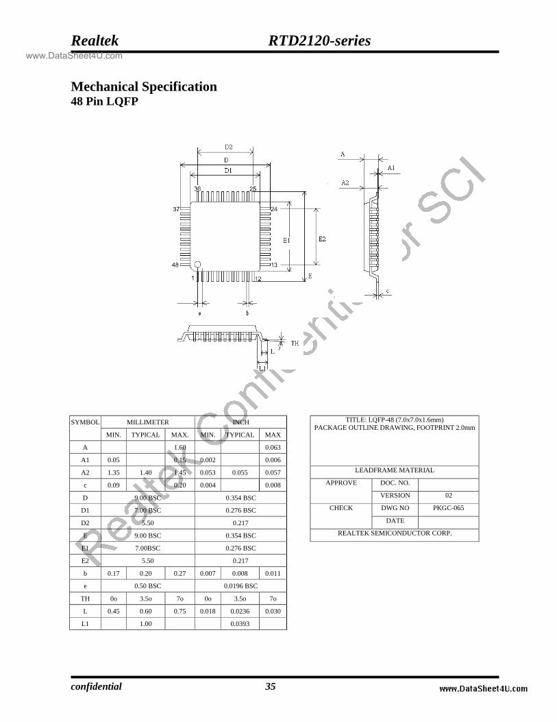
Mechanical Specification 48 Pin LQFP
MILLIMETER INCH SYMBOL
MIN. TYPICAL MAX. MIN. TYPICAL MAX
A 1.60 0.063
A1 0.05 0.15 0.002 0.006
TITLE: LQFP-48 (7.0x7.0x1.6mm) PACKAGE OUTLINE DRAWING, FOOTPRINT 2.0mm
A2 1.35 1.40 1.45 0.053 0.055 0.057 LEADFRAME MATERIAL
c 0.09 0.20 0.004 0.008 DOC. NO.
D 9.00 BSC 0.354 BSC
APPROVE
VERSION 02
D1 7.00 BSC 0.276 BSC DWG NO PKGC-065
D2 5.50 0.217
CHECK
DATE
E 9.00 BSC 0.354 BSC REALTEK SEMICONDUCTOR CORP.
E1 7.00BSC 0.276 BSC
E2 5.50 0.217
b 0.17 0.20 0.27 0.007 0.008 0.011
e 0.50 BSC 0.0196 BSC
TH 0o 3.5o 7o 0o 3.5o 7o
L 0.45 0.60 0.75 0.018 0.0236 0.030
L1 1.00 0.0393
L1
L
www.DataSheet4U.com
Realtek RTD2120-series
confidential 36
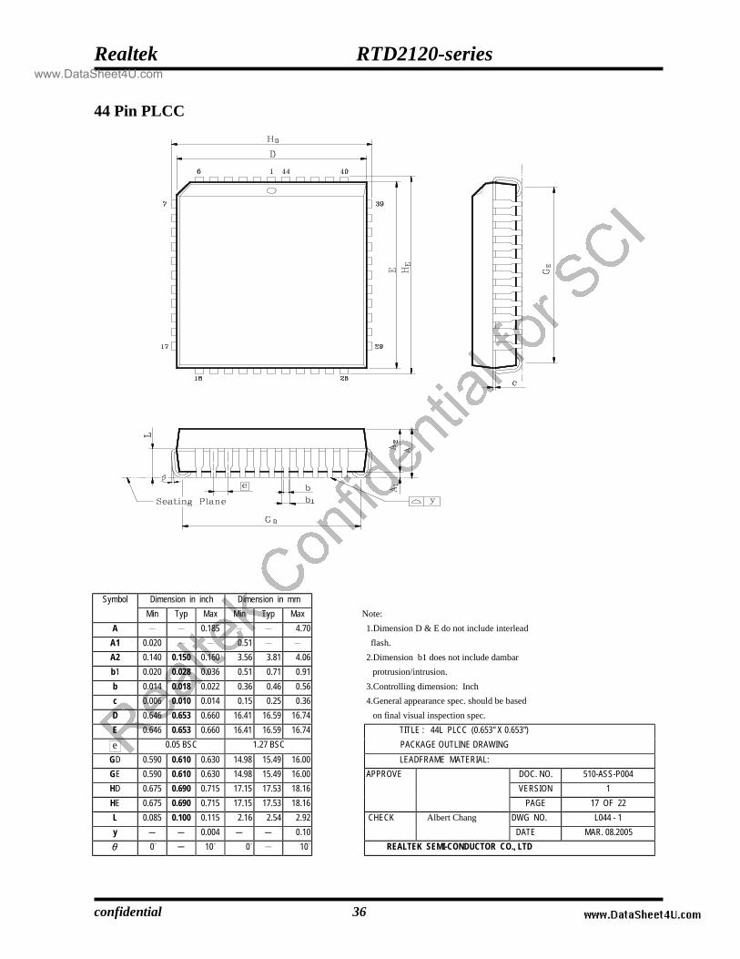
44 Pin PLCC
Symbol Dimension in inch Dimension in mm Min Typ Max Min Typ Max Note:
A - - 0.185 - - 4.70 1.Dimension D & E do not include interlead A1 0.020 - - 0.51 - - flash. A2 0.140 0.150 0.160 3.56 3.81 4.06 2.Dimension b1 does not include dambar b1 0.020 0.028 0.036 0.51 0.71 0.91 protrusion/intrusion. b 0.014 0.018 0.022 0.36 0.46 0.56 3.Controlling dimension: Inch c 0.006 0.010 0.014 0.15 0.25 0.36 4.General appearance spec. should be based D 0.646 0.653 0.660 16.41 16.59 16.74 on final visual inspection spec. E 0.646 0.653 0.660 16.41 16.59 16.74 TITLE : 44L PLCC (0.653" X 0.653") e 0.05 BSC 1.27 BSC PACKAGE OUTLINE DRAWING
GD 0.590 0.610 0.630 14.98 15.49 16.00 LEADFRAME MATERIAL: GE 0.590 0.610 0.630 14.98 15.49 16.00 APPROVE DOC. NO. 510-ASS-P004 HD 0.675 0.690 0.715 17.15 17.53 18.16 VERSION 1 HE 0.675 0.690 0.715 17.15 17.53 18.16 PAGE 17 OF 22 L 0.085 0.100 0.115 2.16 2.54 2.92 CHECK Albert Chang DWG NO. L044 - 1 y - - 0.004 - - 0.10 DATE MAR. 08.2005 θ 0° - 10° 0° - 10° REALTEK SEMI-CONDUCTOR CO., LTD
www.DataSheet4U.com
Realtek RTD2120-series
confidential 37
Ordering Information: The available RTD2120 related products are listed below: Part No. Flash Size Package Type
RTD2120K 96K byte 44 QFP RTD2120L 96K byte 48 LQFP RTD2120S 96K byte 44 PLCC RTD2120L-LF 96K byte 48 LQFP (lead free) RTD2120S-LF 96K byte 44 PLCC (lead free)
www.DataSheet4U.com