rtl design of a generic pseudonoise generatorcradpdf.drdc-rddc.gc.ca/pdfs/unc82/p522715.pdf · rtl...
TRANSCRIPT
RTL Design of a Generic Pseudonoise Generator
Jean-François Beaumont
Defence R&D Canada √ Ottawa TECHNICAL MEMORANDUM
DRDC Ottawa TM 2004-176 September 2004

RTL design of a generic pseudonoisegenerator
Jean-Francois Beaumont
Defence R&D Canada – OttawaTechnical Memorandum
DRDC Ottawa TM 2004-176
September 2004

Her Majesty the Queen as represented by the Minister of National Defence, 2004
Sa majeste la reine, representee par le ministre de la Defense nationale, 2004
Abstract
Pseudonoise (PN) generators have many applications in the field of digital signal proces-sing, especially in wireless communication systems. They are usually implemented in hard-ware through the use of Linear Feedback Shift Registers (LFSR) in either Application Spe-cific Integrated Circuits (ASICs), Field Programmable Gate Array (FPGAs) or ComplexProgrammable Logic Devices (CPLDs).
Although the methods and techniques to code the Register Transfer Level (RTL) algorithmwith a Hardware Description Language (HDL) are currently well known in the design com-munity, this technical memorandum presents an innovative code implementation. This newalgorithm is a generic PN generator that takes as input the polynomial and its associateddegree and, using current synthesis tools, generates a compact area circuit. Results showthat the generated circuit does not consume more logic resources than a traditional hard-coded PN generator. The net advantage of using this new algorithm over its predecessor issignificant savings in terms of design time, verification time and hence, development costs.
Resum e
Les generateurs de bruit pseudoaleatoire ont plusieurs applications dans le domaine dutraitement de signal numerique, particulierement dans les systemes de communication sans-fil. Ils sont generalement mis en oeuvre sous forme materielle par l’entremise de registresa decalagea rebouclage lineaire soit dans des circuits integres specifiques (ASICs), desmatrices prediffusees programmables (FPGAs) ou des reseaux logiques programmablescomplexes (CPLDs).
Bien que les methodes et techniques pour coder l’algorithme au niveau du transfert deregistrea registre (RTL) avec un langage de description materiel (HDL) sont actuellementbien connus dans le milieu de la conception materielle, ce memorandum technique presenteune implementation par codage innovatrice. Ce nouvel algorithme est celui d’un generateurde bruit pseudoaleatoire generique prenant comme donnees d’entrees le polynome et ledegre de celui-ci et qui, en utilisant des outils de synthese actuels, genere un circuita espacecompact. Les resultats montrent que le circuit genere ne consomme pas plus de ressourceslogiques qu’un traditionnel generateur de bruit aleatoire code en dur. L’avantage resultant del’utilisation de ce nouvel algorithme par rapporta ses predecesseurs se traduit eneconomiesappreciables au niveau du temps pour la conception et la verification ainsi qu’au niveau descouts de developpement.
DRDC Ottawa TM 2004-176 i

This page intentionally left blank.
ii DRDC Ottawa TM 2004-176
Executive summary
Digital signal processing for wireless communication systems is an area where DRDCOttawa has developed considerable expertise over the past years and still continues to ex-pand. Part of the ongoing research activity in this area focuses on the development of algo-rithms for the major wireless communication systems on software radio platforms. Sincethe communication standards for these systems are constantly evolving, the current trend inthe industry is to move towards the software radio approach. This technical memorandumpresents one of these algorithms: a Register Transfert Level (RTL) generic pseudonoisegenerator.
Pseudonoise (PN) sequences are widely used in the field of digital signal processing, es-pecially in wireless communication systems. Typically, PN generators are implemented inhardware through the use of Linear Feedback Shift Registers (LFSR) in either ApplicationSpecific Integrated Circuits (ASICs), Field Programmable Gate Array (FPGAs) or Com-plex Programmable Logic Devices (CPLDs). The algorithm description of the circuit iscoded at the RTL via a Hardware Description Language (HDL), such as Verilog or VHDL,and the synthesis is performed with the synthesis tool generally provided with the vendor’ssoftware toolkit of the targeted device.
Although the methodology to code the PN generator RTL algorithm with an HDL languageis currently well known in the design community, this technical memorandum presents aninnovative way to code this algorithm. This new algorithm is one of a generic PN generatorwhere the specific polynomial and its associated degree are presented as inputs to gene-rate the correct circuit in a very compact form, when synthesized with the modern existingsynthesis tools. Simulations were run with different polynomials to verify that the circuitgenerates the correct expected sequence. To verify the logic resource utilization in thedevice, a Xilinx Spartan II FPGA was targeted to synthesize the circuit using polynomialsof various degree and complexity. The results show that the generic circuit generates thecorrect sequence in all cases and consumes the same amount of logic resources as thetraditional hardcoded implementation.
The advantage of this algorithm over its predecessors is that a single VHDL component isrequired to produce many PN generators with different polynomials and degree within thesame design. The user instantiates the same component for all the different PN generators,provides to each of them their specific polynomial and associated degree, and is limited onlyby the available device ressources. The VHDL compiler and the synthesis tool generate thecorrect circuits, significantly reducing design, verification and maintenance time.
Jean-Francois Beaumont. 2004. RTL design of a generic pseudonoise generator. DRDCOttawa TM 2004-176. Defence R&D Canada – Ottawa.
DRDC Ottawa TM 2004-176 iii
Sommaire
Le traitement des signaux numeriques pour les systemes de communication sans-fil est unsecteur ou RDDC Ottawa a developpe une expertise considerable au cours des dernieresannees et qui continue sans cesse de croıtre. Une partie des activites de recherche encours dans ce secteur se concentre sur le developpement d’algorithmes pour les princi-paux systemes de communications sans-fil sur des plateformes de radio realisee logiciel.Puisque les normes sur les communications pour ces systemes sont en constanteevolution,la tendance actuelle dans l’industrie est de se diriger vers l’approche radio realisee logiciel.Ce memorandum technique presente l’un de ces algorithmes : un generateur RTL de bruitpseudoaleatoire (BP) generique.
Les sequences pseudoaleatoires sont largement utilisees dans le domaine du traitement designal numerique, particulierement dans les systemes de communication sans-fil. Generale-ment, les generateurs BP sont mis en oeuvre sous forme materielle par l’entremise de re-gistresa decalagea rebouclage lineaire soit dans des circuits integres specifiques (ASICs),des matrices prediffusees programmables (FPGAs) ou des reseaux logiques programmablescomplexes (CPLDs). La description du circuit sous forme algorithmique est codee au ni-veau du transfert de registrea registre (RTL) via un langage de description materiel (HDL),tel que Verilog ou VHDL, et la synthese est effectuee a l’aide d’un outil de synthesegeneralement fourni avec la trousse de logiciels du fabricant pour le composant selectionne.
Bien que la methodologie pour coder l’algorithme du generateur BP avec un langage HDLest actuellement bien connue dans le milieu de la conception materielle, ce memorandumtechnique presente une facon innovatrice de coder cet algorithme. Ce nouvel algorithme estcelui d’un generateur BP generique ou le polynome specifique et son degre sont les donneesd’entrees servanta generer le bon circuit sous forme compact, lorsque synthetise avec lesoutils modernes de synthese existants. Des simulations furent effectuees avec differentspolynomes afin de verifier que le circuit genere la sequence prevue exacte. Afin de verifierl’utilisation des ressources logiques du composant, un FPGA Spartan II de Xilinx fut choisipour effectuer la synthese du circuit en utilisant des polynomes de degre et de complexitediff erents. Les resultats ont montre que le circuit generique generait dans tous les cas lasequence exacte et utilisait la meme quantite de ressources logiques que l’implementationtradionnelle codee en dur.
L’avantage de cet algorithme sur ses predecesseurs est qu’un seul constituant VHDL estrequis pour produire plusieurs generateurs BP de polynome et de degre differents dans lememe design. L’utilisateur instancie le meme constituant pour tous les differents genera-teurs BP, fournita chacun leur polynome specifique et le degre y etant associe, et est limiteuniquement par les ressources disponibles dans le composant. Le compilateur VHDL etl’outil de synthese genere les circuits exacts, reduisant ainsi significativement le temps deconception, de verification et d’entretien.
Jean-Francois Beaumont. 2004. RTL design of a generic pseudonoise generator. DRDCOttawa TM 2004-176. R & D pour la defense Canada – Ottawa.
iv DRDC Ottawa TM 2004-176
Table of contents
Abstract . . . . . . . . . . . . . . . . . . . . . . . . . . . . . . . . . . . . . . . . . i
Resume . . . . . . . . . . . . . . . . . . . . . . . . . . . . . . . . . . . . . . . . . i
Executive summary . . . . . . . . . . . . . . . . . . . . . . . . . . . . . . . . . . . iii
Sommaire . . . . . . . . . . . . . . . . . . . . . . . . . . . . . . . . . . . . . . . . iv
Table of contents . . . . . . . . . . . . . . . . . . . . . . . . . . . . . . . . . . . . v
List of figures . . . . . . . . . . . . . . . . . . . . . . . . . . . . . . . . . . . . . . vi
List of tables . . . . . . . . . . . . . . . . . . . . . . . . . . . . . . . . . . . . . . . vii
1 Introduction . . . . . . . . . . . . . . . . . . . . . . . . . . . . . . . . . . . 1
2 Pseudonoise generator implementation . . . . . . . . . . . . . . . . . . . . 3
2.1 Theory . . . . . . . . . . . . . . . . . . . . . . . . . . . . . . . . . 3
2.2 General mechanization of the irreducible polynomial . . . . . . . . 4
2.3 Conventional hardware implementation . . . . . . . . . . . . . . . . 4
2.4 Proposed architecture . . . . . . . . . . . . . . . . . . . . . . . . . 6
2.5 Circuit optimizations . . . . . . . . . . . . . . . . . . . . . . . . . 9
3 Verification and results . . . . . . . . . . . . . . . . . . . . . . . . . . . . . 11
3.1 Simulations . . . . . . . . . . . . . . . . . . . . . . . . . . . . . . 11
3.2 Synthesis (hardware implementation) . . . . . . . . . . . . . . . . . 14
4 Conclusion . . . . . . . . . . . . . . . . . . . . . . . . . . . . . . . . . . . 18
References . . . . . . . . . . . . . . . . . . . . . . . . . . . . . . . . . . . . . . . . 19
List of acronyms . . . . . . . . . . . . . . . . . . . . . . . . . . . . . . . . . . . . 20
DRDC Ottawa TM 2004-176 v
List of figures
Figure 1. SSRG configuration . . . . . . . . . . . . . . . . . . . . . . . . . . . . . . 3
Figure 2. MSRG configuration . . . . . . . . . . . . . . . . . . . . . . . . . . . . . 4
Figure 3. Optimized hardware implementation of polynomialf (x) = 1+x3 +x5 . . . 5
Figure 4. Generic Cell (GCi) with unknown combinatorial logic cloud . . . . . . . . 6
Figure 5. Karnaugh map for logic circuit synthesis of Generic Cell’s cloud . . . . . . 7
Figure 6. Generic Cell (GCi) . . . . . . . . . . . . . . . . . . . . . . . . . . . . . . 8
Figure 7. Generic PN generator circuit for a polynomial of degree 5 . . . . . . . . . 9
Figure 8. Simulation results for polynomialsf1(x) and f2(x) . . . . . . . . . . . . . 13
vi DRDC Ottawa TM 2004-176
List of tables
Table 1. Truth table for logic circuit inside the Generic Cell’s cloud . . . . . . . . . 7
Table 2. AND gate truth table . . . . . . . . . . . . . . . . . . . . . . . . . . . . . . 8
Table 3. XOR gate truth table . . . . . . . . . . . . . . . . . . . . . . . . . . . . . . 8
Table 4. Synthesis results for polynomial #1 (f1(x)) using the three design methods . 15
Table 5. Synthesis results for polynomial #2 (f2(x)) using the three design methods . 15
Table 6. Synthesis results for polynomial #3 (f3(x)) using the three design methods . 16
Table 7. Synthesis results for polynomial #4 (f4(x)) using the three design methods . 16
DRDC Ottawa TM 2004-176 vii

This page intentionally left blank.
viii DRDC Ottawa TM 2004-176
1 Introduction
Pseudonoise (PN) sequences are widely used in many areas of Digital Signal Processing.A few examples are in radar, error correction, cryptography, Global Positioning Systems(GPS), Very Small Aperture Satellite Terminals (VSAT) and digital communication sys-tems. One good example of a PN sequence application in digital communications is in theCDMA IS-95 system where they are use to “spread” and “despread” the signal in the spreadspectrum modulation and demodulation operations [1, 2, 3]. They are also very often usedto simply generate gaussian noise for any kind of digital device testing.
The most typical way of implementing PN sequences in hardware (PN generators) isthrough the usage of Linear Feedback Shift Registers (LFSR) [4] in either ApplicationSpecific Integrated Circuits (ASICs), Field Programmable Gate Array (FPGAs) or Com-plex Programmable Logic Devices (CPLDs). The usual method to build such circuits inthose devices is to use a Hardware Description Language (HDL), like Verilog or VHDL, tocode them at the Register Transfer Level (RTL) and synthesize them with a synthesis tool,provided usually with the device vendor’s tools. Another easier alternative is to directly usea predesigned core provided with the device vendor’s tools, instead of HDL coding, andperform the synthesis.
Both of these methods have their pros and cons. The advantage of manually coding thecircuit with a HDL language is that it is device independent, implying that the same codecan be ported to any appropriate device regardless of vendor. However, this method ismore time consuming than directly using a vendor specific predesigned core. In addition tocoding the circuit, the designer must also verify expected functionality.
On the other hand, the use of a predesigned core is more straightforward, as they are pro-vided for free with most vendor’s development tools, and they have been verified, ensuringreliable output. The designer simply has to provide the correct information (like the poly-nomial) to generate an area and speed optimized circuit for the targeted device. However,the disadvantage of this method is that the design is not device independent. If changesare required during simulations, the core must be regenerated again with a different soft-ware tool, external to the simulator. Since the core generator software is external to theHDL simulator, simulation with different polynomial values causes changes to be made intwo steps: regenerating the core and recompiling. This is more time consuming than sim-ply changing the HDL code and recompiling. Additionally, the predesigned core approachcannot be use to create a generic circuit.
The development of a device independent RTL design includes production and testing. Thereduction of development time gives rise to the desire to have a generic circuit that fits anypolynomial. Such generic HDL based designs have already been proposed in the literature[5]. However, these circuits hardcode a finite number of polynomials within the designentity. This type of design, requires some overhead, consumes extra logic resources andlimits the user in his choice of polynomials. Some of these require modification of thedesign to get the desired polynomial, which can introduce errors.
DRDC Ottawa TM 2004-176 1
This technical memorandum presents a novel architecture for a RTL based PN generator.Unlike the existing designs, this new architecture does not hardcode the polynomials withinthe circuit entity but takes the polynomial and its associated degree as inputs to generatea compact area circuit (without extra overhead) when synthesized with the current synthe-sis tools. The circuit is designed in VHDL and is based on the Modular Shift RegisterGenerator (MSRG) configuration, also known as the “Galois” configuration.
The net advantage of this approach is that a single VHDL component can be instantiatedmany times in a design for PN generators having different polynomials of various degree(from 2 and up to the limit imposed by the silicon size). This approach reduces design,debug and maintenance time for systems having many PN generators with different poly-nomials of various degree. The user is merely required to instantiate the same componentfor all the different PN generators. The polynomial and its associated degree are providedas inputs to each instantiated component. The VHDL compiler and the synthesis tool gene-rates the correct circuit.
Also, because of the generic circuit’s architecture and the logic circuit optimization per-formance of today’s HDL synthesis tools, the synthesis results obtained in this technicalmemorandum show that the silicon utilization area is the same as if the circuit was manu-ally coded and customized for the given polynomials.
This design can be implemented in CPLD, FPGA and ASIC devices. For the purpose ofthis technical memorandum, simulations were run with different polynomials to verify itscorrect functionality. To verify the silicon utilization area in a component, synthesis wasperformed, targeting a Xilinx Spartan II FPGA, with polynomials of various degree andcomplexity.
2 DRDC Ottawa TM 2004-176
2 Pseudonoise generator implementation
2.1 Theory
An LFSR based PN generator withn stages will always produce a periodic output sequence.The initial condition of the shift register will eventually be reproduced after a finite numberof clock cycles. The period cannot be greater than 2n (maximum number of combinationsof n binary digits). However, due to the architecture of this type of generator, the all-zerocondition does not occur, unless set as the initial condition. In this case, the generator willremain in the same state forever. Therefore, the maximum number of possible states is2n− 1. A generator output with such a period is called a “maximal length sequence” or“m-sequence”. The higher the number of stages, the longer the sequence will be and themore random it will appear. For that reason, they are also called “pseudorandom noise”generators.
Each PN sequence can be described by a binary irreducible primitive polynomial of theform:
f (x) = 1+c1x+c2x2 + · · ·+cixi + · · ·+cn−1xn−1 +xn, ci ∈ GF(2) (1)
WhereGF(2) is a binary Galois Field (two elements, 0 and 1).
There are two different ways of implementing in hardware the irreducible (primitive) poly-nomial as an LFSR: The Simple Shift Register Generator (SSRG), also known as the “Fi-bonacci configuration” and the Modular Shift Register Generator (MSRG), also known asthe “Galois configuration”. Figure 1 and Figure 2 illustrate both configurations. The scopeof this technical memorandum is limited to the generic PN generator circuit based on theMSRG configuration.
R1
C1
x
R2
C2
x2
Ci-1
Ri
Ci
xi
Cn-2
Rn-1
Cn-1
Xn-1
Rn
Xn
clock
Figure 1: SSRG configuration
DRDC Ottawa TM 2004-176 3
R1
C1
x
R2
C2
x2
Ci-1
Ri
Ci
xi
Cn-2
Rn-1
Cn-1
Xn-1
Rn
Xn
clock
Figure 2: MSRG configuration
2.2 General mechanization of the irreducible polynomial
Considering only the MSRG configuration, the “mechanization” of the irreducible polyno-mial is accomplished using binary storage elements and modulo-2 adders [1]. Referring toFigure 2, the binary storage elements of the LFSR are designated asR1, R2, . . ., Rn. Thecoefficients of the polynomial, designated asC1, C2, . . ., Cn−1, play the roles of “switches”that dictate whether or not the output of the last stageRn is modulo-2 added to the stageRi .If the value ofCi is “0”, the output of the stageRi is simply shifted to the next stageRi+1.If the value ofCi is “1”, the output of the stageRi is modulo-2 added toRn and fed to thenext stageRi+1. Only the input of the first stageR1 is connected directly to the output of thelast stageRn. Each register stageRi is associated with the power termxi of the irreduciblepolynomial.
The operation of the LFSR is initiated by the loading of an-tuple vector in then-stageregister. Once the initial vector is loaded, the LFSR starts generating the sequence at therate specified by the clock connected to the binary storage elements. A non-zeron-tupleloading vector will produce 2n−1 distinct vectors in the registers, periodically, as the clockruns. The sequence resulting from the output, taken from the last stageRn, is a PN sequenceof length 2n−1, which is one version (phase shift) out of 2n−1 possible sequences. Thisunique sequence depends on the choice of then-tuple loading vector, which is again a oneout of 2n−1 possible choices.
2.3 Conventional hardware implementation
Usually, PN generators are utilized within complex systems that are implemented in eithercustom silicon devices like ASICs or in programmable devices like FPGAs and CPLDs.As a result, their implementation is typically done using an HDL language such as VHDLwhich makes them device independant. The logic circuit described in VHDL is synthesizedusing software tools taking the code as input and mapping it to gates in the silicon orprogrammable device.
To better illustrate how an irreducible polynomial is implemented in hardware, let’s takethe following simple polynomial of degree 5:
4 DRDC Ottawa TM 2004-176
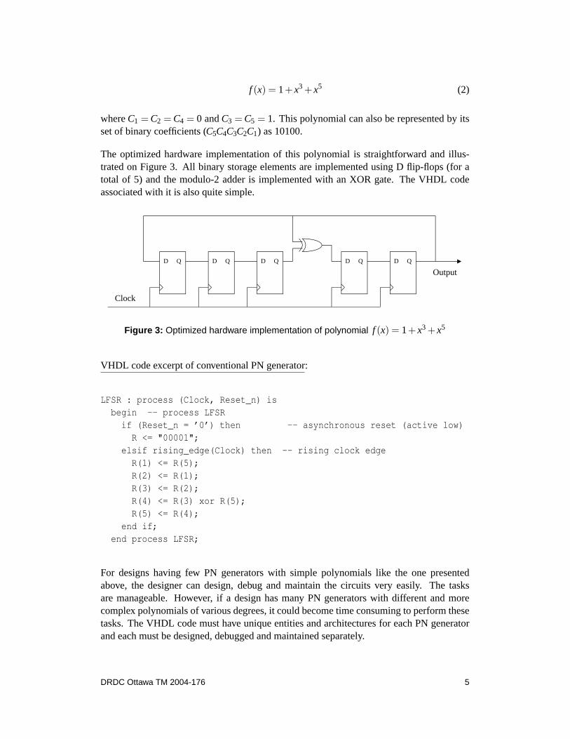
f (x) = 1+x3 +x5 (2)
whereC1 = C2 = C4 = 0 andC3 = C5 = 1. This polynomial can also be represented by itsset of binary coefficients (C5C4C3C2C1) as 10100.
The optimized hardware implementation of this polynomial is straightforward and illus-trated on Figure 3. All binary storage elements are implemented using D flip-flops (for atotal of 5) and the modulo-2 adder is implemented with an XOR gate. The VHDL codeassociated with it is also quite simple.
D Q D Q D Q D Q D Q
Clock
Output
Figure 3: Optimized hardware implementation of polynomial f (x) = 1+x3 +x5
VHDL code excerpt of conventional PN generator:
LFSR : process (Clock, Reset_n) isbegin -- process LFSR
if (Reset_n = ’0’) then -- asynchronous reset (active low)R <= "00001";
elsif rising_edge(Clock) then -- rising clock edgeR(1) <= R(5);R(2) <= R(1);R(3) <= R(2);R(4) <= R(3) xor R(5);R(5) <= R(4);
end if;end process LFSR;
For designs having few PN generators with simple polynomials like the one presentedabove, the designer can design, debug and maintain the circuits very easily. The tasksare manageable. However, if a design has many PN generators with different and morecomplex polynomials of various degrees, it could become time consuming to perform thesetasks. The VHDL code must have unique entities and architectures for each PN generatorand each must be designed, debugged and maintained separately.
DRDC Ottawa TM 2004-176 5
It would be much simpler for the designer if a single generic component could be usedfor all the different PN generators in the design. This component would only need asinput the polynomial and its degree (supplied at the instance level by the user) and theVHDL compiler and synthesis tool would generate automatically the circuit described bythe polynomial.
To give an idea, it would take a few hours for an experienced HDL designer to manuallycode and verify the three code generators of the CDMA IS-95 system. Using a generic PNgenerator, these tasks are performed in a fraction of the time with the added benefit of aHDL implementation. This time savings is directly proportional to the number and the sizeof the PN generators in the system.
Also, knowing that PN generators have applications in many other areas (like in radar, cryp-tography, error correction and 3G cellular systems), a generic circuit like the one proposedwould be beneficial, especially if these systems use more PN generators in their futuredesigns.
2.4 Proposed architecture
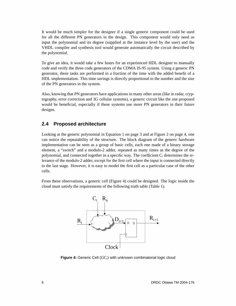
Looking at the generic polynomial in Equation 1 on page 3 and at Figure 2 on page 4, onecan notice the repeatability of the structure. The block diagram of the generic hardwareimplementation can be seen as a group of basic cells, each one made of a binary storageelement, a “switch” and a modulo-2 adder, repeated as many times as the degree of thepolynomial, and connected together in a specific way. The coefficientCi determines the re-levance of the modulo-2 adder, except for the first cell where the input is connected directlyto the last stage. However, it is easy to model the first cell as a particular case of the othercells.
From these observations, a generic cell (Figure 4) could be designed. The logic inside thecloud must satisfy the requirements of the following truth table (Table 1).
D QRi
Ci Rn
Di+1Ri+1
Clock
Figure 4: Generic Cell (GCi) with unknown combinatorial logic cloud
6 DRDC Ottawa TM 2004-176
Ci Rn Ri Di+1
0 0 0 00 0 1 10 1 0 00 1 1 11 0 0 01 0 1 11 1 0 11 1 1 0
Table 1: Truth table for logic circuit inside the Generic Cell’s cloud
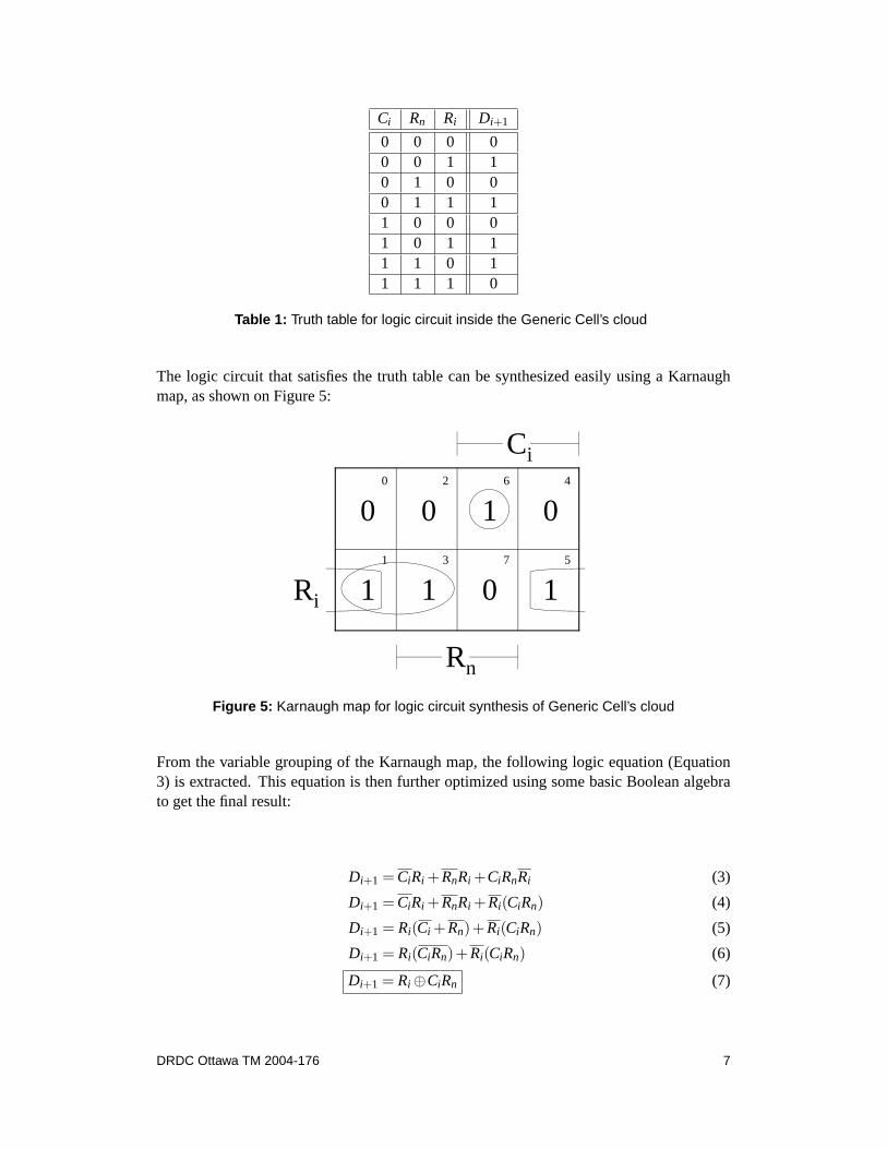
The logic circuit that satisfies the truth table can be synthesized easily using a Karnaughmap, as shown on Figure 5:
00
02
11
13
16
07
04
15
Ci
Rn
Ri
Figure 5: Karnaugh map for logic circuit synthesis of Generic Cell’s cloud
From the variable grouping of the Karnaugh map, the following logic equation (Equation3) is extracted. This equation is then further optimized using some basic Boolean algebrato get the final result:
Di+1 = CiRi +RnRi +CiRnRi (3)
Di+1 = CiRi +RnRi +Ri(CiRn) (4)
Di+1 = Ri(Ci +Rn)+Ri(CiRn) (5)
Di+1 = Ri(CiRn)+Ri(CiRn) (6)
Di+1 = Ri ⊕CiRn (7)
DRDC Ottawa TM 2004-176 7
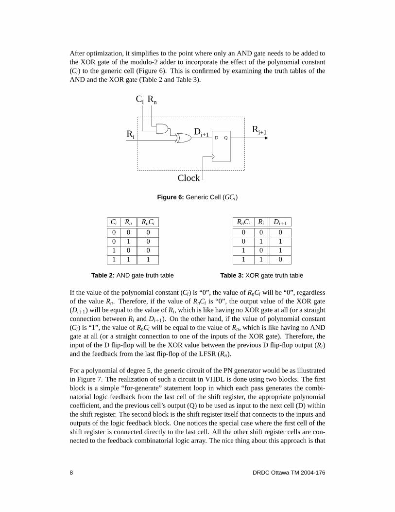
After optimization, it simplifies to the point where only an AND gate needs to be added tothe XOR gate of the modulo-2 adder to incorporate the effect of the polynomial constant(Ci) to the generic cell (Figure 6). This is confirmed by examining the truth tables of theAND and the XOR gate (Table 2 and Table 3).
D QRi
Ci Rn
Di+1Ri+1
Clock
Figure 6: Generic Cell (GCi)
Ci Rn RnCi
0 0 00 1 01 0 01 1 1
Table 2: AND gate truth table
RnCi Ri Di+1
0 0 00 1 11 0 11 1 0
Table 3: XOR gate truth table
If the value of the polynomial constant (Ci) is “0”, the value ofRnCi will be “0”, regardlessof the valueRn. Therefore, if the value ofRnCi is “0”, the output value of the XOR gate(Di+1) will be equal to the value ofRi , which is like having no XOR gate at all (or a straightconnection betweenRi andDi+1). On the other hand, if the value of polynomial constant(Ci) is “1”, the value ofRnCi will be equal to the value ofRn, which is like having no ANDgate at all (or a straight connection to one of the inputs of the XOR gate). Therefore, theinput of the D flip-flop will be the XOR value between the previous D flip-flop output (Ri)and the feedback from the last flip-flop of the LFSR (Rn).
For a polynomial of degree 5, the generic circuit of the PN generator would be as illustratedin Figure 7. The realization of such a circuit in VHDL is done using two blocks. The firstblock is a simple “for-generate” statement loop in which each pass generates the combi-natorial logic feedback from the last cell of the shift register, the appropriate polynomialcoefficient, and the previous cell’s output (Q) to be used as input to the next cell (D) withinthe shift register. The second block is the shift register itself that connects to the inputs andoutputs of the logic feedback block. One notices the special case where the first cell of theshift register is connected directly to the last cell. All the other shift register cells are con-nected to the feedback combinatorial logic array. The nice thing about this approach is that
8 DRDC Ottawa TM 2004-176
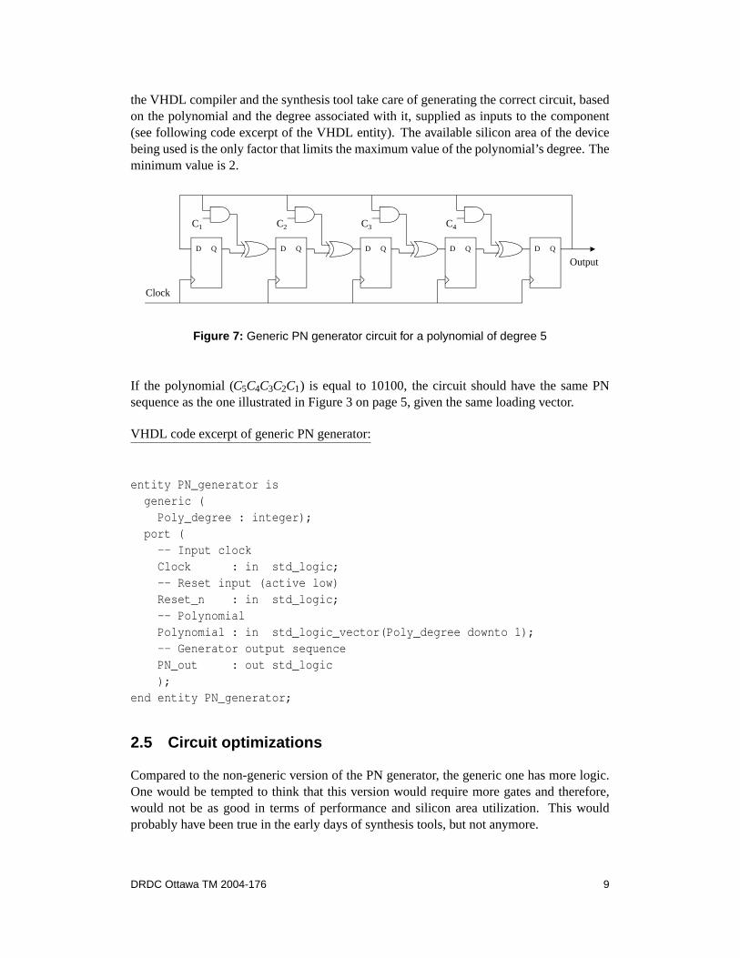
the VHDL compiler and the synthesis tool take care of generating the correct circuit, basedon the polynomial and the degree associated with it, supplied as inputs to the component(see following code excerpt of the VHDL entity). The available silicon area of the devicebeing used is the only factor that limits the maximum value of the polynomial’s degree. Theminimum value is 2.
D Q
Clock
Output
C1
D Q
C2
D Q
C3
D Q
C4
D Q
Figure 7: Generic PN generator circuit for a polynomial of degree 5
If the polynomial (C5C4C3C2C1) is equal to 10100, the circuit should have the same PNsequence as the one illustrated in Figure 3 on page 5, given the same loading vector.
VHDL code excerpt of generic PN generator:
entity PN_generator isgeneric (Poly_degree : integer);
port (-- Input clockClock : in std_logic;-- Reset input (active low)Reset_n : in std_logic;-- PolynomialPolynomial : in std_logic_vector(Poly_degree downto 1);-- Generator output sequencePN_out : out std_logic);
end entity PN_generator;
2.5 Circuit optimizations
Compared to the non-generic version of the PN generator, the generic one has more logic.One would be tempted to think that this version would require more gates and therefore,would not be as good in terms of performance and silicon area utilization. This wouldprobably have been true in the early days of synthesis tools, but not anymore.
DRDC Ottawa TM 2004-176 9
Today’s synthesis tools are more efficient and can now optimize away unnecessary gatesused in a design. This is especially true in the case where the polynomials are defined asconstants, like in the generic PN generator. In this case, the input values of the “AND” andthe “XOR” gates of each generic cell are static. Depending on their input values, some ofthese gates can be removed from the circuit without affecting its functionality. Therefore,the synthesis of a PN generator with a defined polynomial should lead to the same resultwhether it has been designed using the conventional way or with the generic circuit. It iseasy to verify by using the RTL schematic viewer (in most of today’s synthesis softwaretools) and comparing both results. Another, (and better) way to verify this is to consult thetool’s synthesis and mapping reports to verify the quantity of logic resources that have beenutilized.
It is very important to understand that the optimization relies entirely on the fact that thepolynomial values are defined as constant at the instance level. If the polynomial values arenot defined as constants, this optimization will not occur.
10 DRDC Ottawa TM 2004-176
3 Verification and results
3.1 Simulations
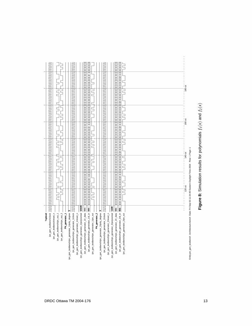
To verify the correct functionality of the generic PN generator, polynomial values neededto be chosen. Since the sequence length is equal to 2n−1 for a maximal length sequence,the verification takes greater time if the polynomial degree is high. Also, based on thetechnique used to generate the circuit (for-generate loop), a high polynomial degree is notrequired to verify the circuit functionality. A polynomial of degree four or five is suffi-cient. Any problem within the circuit be apparent early in the verification process, since asingle incorrect bit in the sequence will fail the test. Therefore, the following two simplepolynomials (f(x)) were used to verify the functionality of the generic PN generator.
The first objective was to verify that the selected polynomials could produce the expectedsequences (S) given specific initial loading vectors (L)1. The second objective was todemonstrate that only a single VHDL component of the generic PN generator was needed ina system having more than one PN generator with different polynomials of various degrees.
Polynomial #1:
f1(x) = 1+x3 +x5
S1 = 0000101011101100011111001101001L1 = 00001
Polynomial #2:
f2(x) = 1+x3 +x4
S2 = 000111101011001L2 = 0001
To achieve these two objectives, a VHDL testbench with two instances of the generic PNgenerator component was created (see following VHDL excerpt code). The first instanceused polynomial #1 and the second instance polynomial #2. Both generators were run witha 1 MHz clock for a period of 10 ms to permit the periodicity of the sequences. A resetsignal was periodically set to see the behavior of the generator during and after the reset.The reset was 10 us long and repeated every 100 us. Both instances of the PN generatorbehaved as expected. Figure 8 shows the results obtained from simulations.
1L = {Rn,Rn−1, . . . ,R2,R1}, where n is the polynomial degree andRi a register of the LFSR
DRDC Ottawa TM 2004-176 11
VHDL code excerpt of testbench:
-- Polynomials definition
-- First polynomial-- F1(x) = xˆ5 + xˆ3 + 1 = 1*xˆ5 + 0*xˆ4 + 1*xˆ3 + 0*xˆ2 + 0*xˆ1 + 1constant F1_degree : integer := 5; -- Polynomial degreeconstant F1 : std_logic_vector(F1_degree downto 1) := "10100";
-- Second polynomial-- F2(x) = xˆ4 + xˆ3 + 1 = 1*xˆ4 + 1*xˆ3 + 0*xˆ2 + 0*xˆ1 + 1constant F2_degree : integer := 4; -- Polynomial degreeconstant F2 : std_logic_vector(F2_degree downto 1) := "1100";
. . .
PN_generator_1 : component PN_generatorgeneric map (Poly_degree => F1_degree)
port map (Clock => Clock,Reset_n => Reset_n,Polynomial => F1,PN_out => PN_out_1);
PN_generator_2 : component PN_generatorgeneric map (Poly_degree => F2_degree)
port map (Clock => Clock,Reset_n => Reset_n,Polynomial => F2,PN_out => PN_out_2);
. . .
12 DRDC Ottawa TM 2004-176
Top
leve
l
PN
_gen
erat
or_1
5 1010
0
0000
1
0001
1100
1100
1100
PN
_gen
erat
or_2
4 1100
0001
001
100
100
100
100
100
100
120
us14
0 us
160
us18
0 us
Top
leve
l
/pn_
gen_
test
benc
h/cl
ock
/pn_
gen_
test
benc
h/re
set_
n
/pn_
gen_
test
benc
h/pn
_out
_1
/pn_
gen_
test
benc
h/pn
_out
_2
PN
_gen
erat
or_1
/pn_
gen_
test
benc
h/pn
_gen
erat
or_1
/pol
y_de
gree
5
/pn_
gen_
test
benc
h/pn
_gen
erat
or_1
/clo
ck
/pn_
gen_
test
benc
h/pn
_gen
erat
or_1
/res
et_n
/pn_
gen_
test
benc
h/pn
_gen
erat
or_1
/pol
ynom
ial
1010
0
/pn_
gen_
test
benc
h/pn
_gen
erat
or_1
/r_d
ata
0000
1
/pn_
gen_
test
benc
h/pn
_gen
erat
or_1
/d_i
n00
0111
0011
0011
00
/pn_
gen_
test
benc
h/pn
_gen
erat
or_1
/pn_
out
PN
_gen
erat
or_2
/pn_
gen_
test
benc
h/pn
_gen
erat
or_2
/pol
y_de
gree
4
/pn_
gen_
test
benc
h/pn
_gen
erat
or_2
/clo
ck
/pn_
gen_
test
benc
h/pn
_gen
erat
or_2
/res
et_n
/pn_
gen_
test
benc
h/pn
_gen
erat
or_2
/pol
ynom
ial
1100
/pn_
gen_
test
benc
h/pn
_gen
erat
or_2
/r_d
ata
0001
/pn_
gen_
test
benc
h/pn
_gen
erat
or_2
/d_i
n00
110
010
010
010
010
010
0
/pn_
gen_
test
benc
h/pn
_gen
erat
or_2
/pn_
out
Ent
ity:p
n_ge
n_te
stbe
nch
Arc
hite
ctur
e:be
nch
Dat
e: F
ri S
ep 0
3 11
:34:
40 E
aste
rn D
aylig
ht T
ime
2004
R
ow: 1
Pag
e: 1
Fig
ure
8:S
imul
atio
nre
sults
for
poly
nom
ials
f 1(x
)an
df 2
(x)
DRDC Ottawa TM 2004-176 13
3.2 Synthesis (hardware implementation)
Most of today’s synthesis tools for ASIC or FPGA devices perform logic optimizations inthe HDL source code. These tools are particularly good for performing the logic optimiza-tions when some of the circuit inputs are constants.
Since the generic PN generator is essentially built around a logic circuit having a constantinput (the polynomial value), it is expected that the synthesis tool can optimize the circuitsuch that the end result would be very close to one where the logic circuit was alreadyoptimum, such as a manually coded and custom PN generator. Also, because of the na-ture of the logic optimization (constant based), the result should be independent of the PNgenerator size (polynomial). Another perspective, is to envision the circuit as a numberof the same generic cell, all connected together and each being optimized the same way(depending on the constant polynomial value).
To verify this assumption, the Xilinx ISE FPGA development toolkit was used. Unlikethe functional verification where a relatively small polynomial was sufficient to verify thealgorithm, it beneficial to have polynomials of various sizes to verify the logic resourceallocation in the device. The device targeted for these synthesis experiments was the XilinxSpartan II XC2S50E-6TQ144. The following four polynomials were used to create the PNgenerators. In order to compare the synthesis results, these PN generators were created withthe three different design methods: the Xilinx core generator, the custom HDL code andthe generic HDL code .
Synthesis verification polynomials:
• f1(x) = 1+x3 +x5
• f2(x) = 1+x5 +x7 +x8 +x9 +x13+x15
• f3(x) = 1+x1 +x2 +x3 +x5 +x6 +x7 +x10+x16+x17+x18+x19+x21+x22+x25+x26+x27+x31+x33+x35+x42
• f4(x) = 1+x1 +x3 +x4 +x64
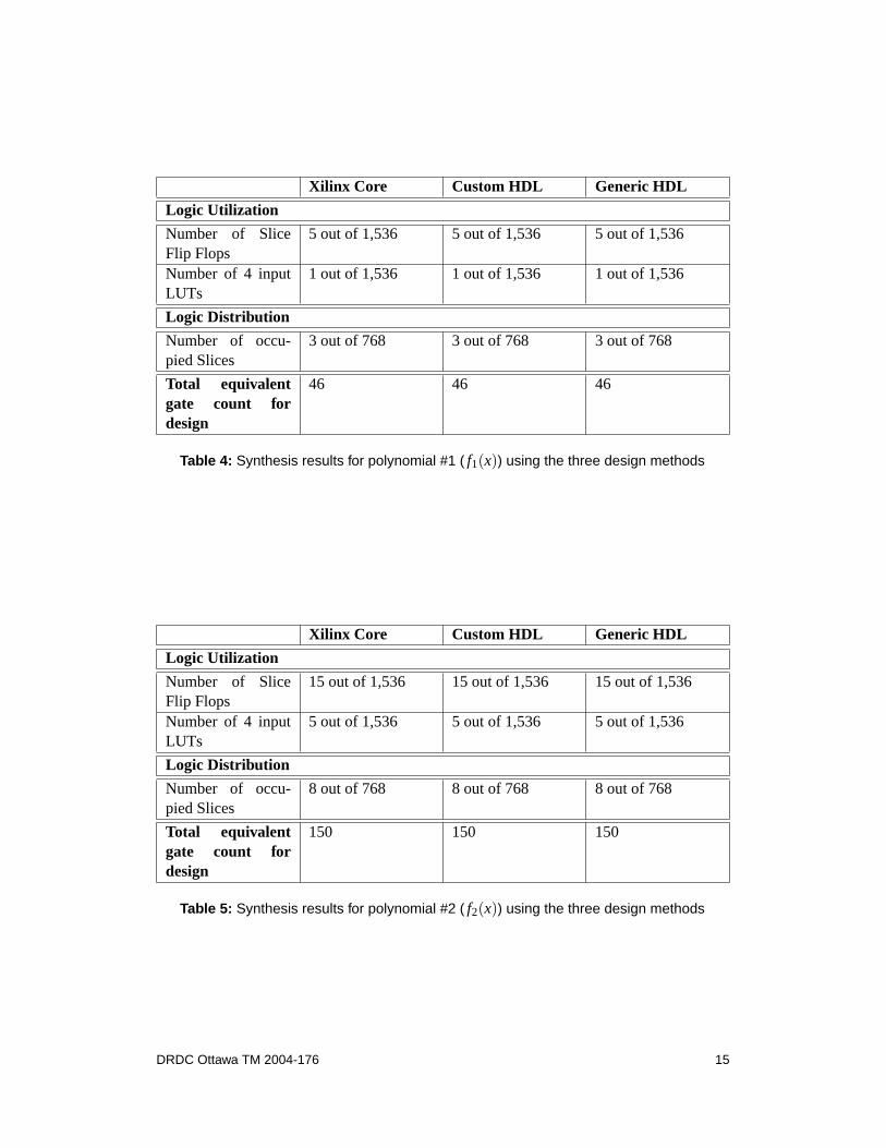
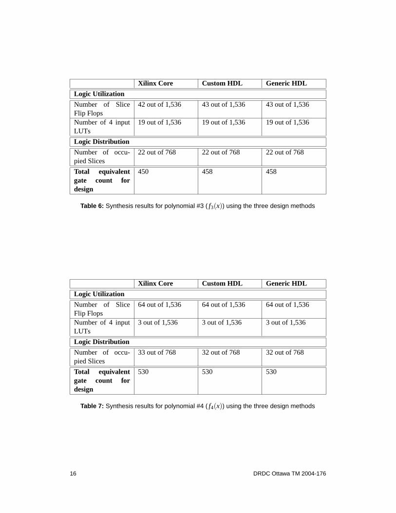
The following tables provides a comparative summary of the results obtained for each ofthe polynomials using the three different methods. These results are taken from the “MapReport” of the Xilinx ISE software toolkit.
14 DRDC Ottawa TM 2004-176
Xilinx Core Custom HDL Generic HDL
Logic Utilization
Number of SliceFlip Flops
5 out of 1,536 5 out of 1,536 5 out of 1,536
Number of 4 inputLUTs
1 out of 1,536 1 out of 1,536 1 out of 1,536
Logic Distribution
Number of occu-pied Slices
3 out of 768 3 out of 768 3 out of 768
Total equivalentgate count fordesign
46 46 46
Table 4: Synthesis results for polynomial #1 ( f1(x)) using the three design methods
Xilinx Core Custom HDL Generic HDL
Logic Utilization
Number of SliceFlip Flops
15 out of 1,536 15 out of 1,536 15 out of 1,536
Number of 4 inputLUTs
5 out of 1,536 5 out of 1,536 5 out of 1,536
Logic Distribution
Number of occu-pied Slices
8 out of 768 8 out of 768 8 out of 768
Total equivalentgate count fordesign
150 150 150
Table 5: Synthesis results for polynomial #2 ( f2(x)) using the three design methods
DRDC Ottawa TM 2004-176 15
Xilinx Core Custom HDL Generic HDL
Logic Utilization
Number of SliceFlip Flops
42 out of 1,536 43 out of 1,536 43 out of 1,536
Number of 4 inputLUTs
19 out of 1,536 19 out of 1,536 19 out of 1,536
Logic Distribution
Number of occu-pied Slices
22 out of 768 22 out of 768 22 out of 768
Total equivalentgate count fordesign
450 458 458
Table 6: Synthesis results for polynomial #3 ( f3(x)) using the three design methods
Xilinx Core Custom HDL Generic HDL
Logic Utilization
Number of SliceFlip Flops
64 out of 1,536 64 out of 1,536 64 out of 1,536
Number of 4 inputLUTs
3 out of 1,536 3 out of 1,536 3 out of 1,536
Logic Distribution
Number of occu-pied Slices
33 out of 768 32 out of 768 32 out of 768
Total equivalentgate count fordesign
530 530 530
Table 7: Synthesis results for polynomial #4 ( f4(x)) using the three design methods
16 DRDC Ottawa TM 2004-176

These results show that there are no differences for the logic utilization and distribution inthe device between a custom HDL design and the generic one. The Xilinx core howeverprovides results that are slightly different, but not significantly. If the SRL16 macro wasused for the design with the Xilinx core, the synthesis results would have been better. How-ever, the circuit would have been different from the custom and the generic design since theusage of the SRL16 macro generates a design with serial loading and without a reset. Forthis reason, core design with the SRL16 macro was not used in the comparison.
DRDC Ottawa TM 2004-176 17
4 Conclusion
With the availability of today’s high density silicon devices, HDL designers are faced withdesigns that are always growing in terms of size and complexity. In order to meet theirtight schedules and milestones, HDL designers are always seeking design methodologiesthat allow:
1. shorter design time
2. shorter verification time
3. optimized design (logic resources utilization)
This technical memorandum presents the design of a generic PN generator that helpsachieve the first two goals. This HDL block is easy to use and has been proven to work, andas a result, will reduce the development and verification time, upon implementation. De-signers who need many different implementations of PN generators in a single RTL baseddesign will find it has several advantages. For example, a designer building a CDMA sys-tem (such as IS-95) where different pseudonoise sequences are needed [1] would find itquite useful. As proposed, only one piece of HDL code needs to be maintained.
Although the architecture cannot guarantee an optimized design (in terms of logic resourcesutilization), the results obtained in this technical memorandum show that one is likely.
The generic PN generator presented here is a basic one. It is possible to add to it otherfeatures like fill vector loading, masking and enabling/disabling capabilities and still keepit sufficiently generic such that all the advantages of using it remain. This is an area ofwork.
Finally, it is also possible to be able to implement this circuit using HDL languages otherthan VHDL. Verilog 2001 and System C are examples of alternatives but testing these wasbeyond the scope of this technical memorandum.
18 DRDC Ottawa TM 2004-176
References
1. Jhong Sam Lee, Leonard E. Miller (1998). CDMA Systemes Engineering Handbook,Artech House.
2. ir.J.Meel (1999). Spread Spectrum. Technical Report. De Nayer Instituut. Jan DeNayerlaan, 5, B-2860 Sint-Katelijne-Waver, Belgium.
3. Schwarz, Richard (2001). An Introduction to Linear Recursive Sequences in SpreadSpectrum Systems. Technical Report. Filtronic Sigtek Inc.
4. Mutagi, R.N. (1996). Pseudo noise sequences for engineers.Electronics &Communications Engineering Journal, pp. 79–87.
5. Smith, Douglas J. (2001). HDL Chip Design, Doone Publications.
DRDC Ottawa TM 2004-176 19
List of acronyms
ASIC Application Specific Integrated CircuitCDMA Code Division Multiple AccessCPLD Complex Programmable Logic DeviceFPGA Field Programmable Gate ArrayGF Galois FieldHDL Hardware Description LanguageIS Interim StandardLFSR Linear Feedback Shift RegisterMSRG Modular Shift Register GeneratorPN Pseudo Noise (or Pseudonoise)RTL Register Transfer LanguageSSRG Simple Shift Register GeneratorVHDL Very high speed integrated circuit (VHSIC) Hardware Description Language
20 DRDC Ottawa TM 2004-176
DOCUMENT CONTROL DATA(Security classification of title, body of abstract and indexing annotation must be entered when document is classified)
1. ORIGINATOR (the name and address of the organization preparing the document.Organizations for whom the document was prepared, e.g. Centre sponsoring acontractor’s report, or tasking agency, are entered in section 8.)
Defence R&D Canada – Ottawa3701, Carling avenue, Ottawa, Ontario, K1A 0Z4
2. SECURITY CLASSIFICATION(overall security classification of the documentincluding special warning terms if applicable).
UNCLASSIFIED
3. TITLE (the complete document title as indicated on the title page. Its classification should be indicated by the appropriateabbreviation (S,C,R or U) in parentheses after the title).
RTL design of a generic pseudonoise generator
4. AUTHORS(Last name, first name, middle initial. If military, show rank, e.g. Doe, Maj. John E.)
Beaumont, Jean-Francois
5. DATE OF PUBLICATION (month and year of publication of document)
September 2004
6a. NO. OF PAGES (totalcontaining information. IncludeAnnexes, Appendices, etc).
31
6b. NO. OF REFS (total cited indocument)
5
7. DESCRIPTIVE NOTES (the category of the document, e.g. technical report, technical note or memorandum. If appropriate, enter the type of report,e.g. interim, progress, summary, annual or final. Give the inclusive dates when a specific reporting period is covered).
Technical Memorandum
8. SPONSORING ACTIVITY (the name of the department project office or laboratory sponsoring the research and development. Include address).
Defence R&D Canada – Ottawa3701, Carling avenue, Ottawa, Ontario, K1A 0Z4
9a. PROJECT OR GRANT NO. (if appropriate, the applicable research anddevelopment project or grant number under which the document waswritten. Specify whether project or grant).
15bl12
9b. CONTRACT NO. (if appropriate, the applicable number under whichthe document was written).
10a. ORIGINATOR’S DOCUMENT NUMBER (the official document numberby which the document is identified by the originating activity. Thisnumber must be unique.)
DRDC Ottawa TM 2004-176
10b. OTHER DOCUMENT NOs. (Any other numbers which may beassigned this document either by the originator or by the sponsor.)
11. DOCUMENT AVAILABILITY (any limitations on further dissemination of the document, other than those imposed by security classification)
( X ) Unlimited distribution( ) Defence departments and defence contractors; further distribution only as approved( ) Defence departments and Canadian defence contractors; further distribution only as approved( ) Government departments and agencies; further distribution only as approved( ) Defence departments; further distribution only as approved( ) Other (please specify):
12. DOCUMENT ANNOUNCEMENT (any limitation to the bibliographic announcement of this document. This will normally correspond to the DocumentAvailability (11). However, where further distribution beyond the audience specified in (11) is possible, a wider announcement audience may beselected).
Full unlimited announcement
13. ABSTRACT (a brief and factual summary of the document. It may also appear elsewhere in the body of the document itself. It is highly desirable that theabstract of classified documents be unclassified. Each paragraph of the abstract shall begin with an indication of the security classification of theinformation in the paragraph (unless the document itself is unclassified) represented as (S), (C), (R), or (U). It is not necessary to include here abstracts inboth official languages unless the text is bilingual).
Pseudonoise (PN) generators have many applications in the field of digital signal processing, especially inwireless communication systems. They are usually implemented in hardware through the use of Linear Feed-back Shift Registers (LFSR) in either Application Specific Integrated Circuits (ASICs), Field ProgrammableGate Array (FPGAs) or Complex Programmable Logic Devices (CPLDs).
Although the methods and techniques to code the Register Transfer Level (RTL) algorithm with a HardwareDescription Language (HDL) are currently well known in the design community, this technical memorandumpresents an innovative code implementation. This new algorithm is a generic PN generator that takes asinput the polynomial and its associated degree and, using current synthesis tools, generates a compact areacircuit. Results show that the generated circuit does not consume more logic resources than a traditionalhardcoded PN generator. The net advantage of using this new algorithm over its predecessor is significantsavings in terms of design time, verification time and hence, development costs.
14. KEYWORDS, DESCRIPTORS or IDENTIFIERS (technically meaningful terms or short phrases that characterize a document and could be helpful incataloguing the document. They should be selected so that no security classification is required. Identifiers, such as equipment model designation, tradename, military project code name, geographic location may also be included. If possible keywords should be selected from a published thesaurus. e.g.Thesaurus of Engineering and Scientific Terms (TEST) and that thesaurus-identified. If it not possible to select indexing terms which are Unclassified, theclassification of each should be indicated as with the title).
Pseudo Noise, Pseudo-noise, Pseudonoise generator, PN generator, Pseudonoise sequences, LFSR, Ge-nerator, ASIC, FPGA, RTL, Xilinx, generic


Defence R&D Canada
Canada’s leader in defenceand national security R&D
Chef de file au Canada en R & Dpour la défense et la sécurité nationale
R & D pour la défense Canada
www.drdc-rddc.gc.ca