s rocessing and manufacturing of components … · 2017-08-17 · 65 chapter 3 synthesis,...
TRANSCRIPT

65
CHAPTER 3
SYNTHESIS, PROCESSING, AND MANUFACTURING OF COMPONENTS, DEVICES, AND SYSTEMS
Chad A. Mirkin, Mark Tuominen19 With contributions from: Matthew R. Jones, Louise R. Giam, Richard Siegel, James Ruud,
Fereshteh Ebrahimi, Sean Murdock, Robert Hwang, Xiang Zhang John Milner, John Belk, Mark Davis, Tadashi Shibata
3.1 VISION FOR THE NEXT DECADE
Changes of Vision over the Previous 10 Years
The last decade has been an exciting period of discovery in the synthesis and processing of nanostructures. Many new nanomaterials have emerged, along with new fabrication processes to generate them. The last decade has seen penetration of nanotechnology into almost every area and discipline in science and engineering. Nanotechnology has been used in commercial products, including nanostructured coatings, cosmetics, textiles and magnetic storage devices, among many others. While such products mark much more purpose-oriented use and application of nanostructures, there also has been important basic research concerning the toolkits for synthesis, fabrication, and patterning of nanostructures, in addition to bioinspired synthesis and directed self-assembly. Many of these advances show great promise for the development of new nanomanufacturing processes that will drive the creation of future nanosystems and devices. For example, the last ten years have seen the development of novel synthesis approaches for a range of nanoscale materials including aerosols, colloids, thin-films, nanocrystalline metals, ceramics, biomaterials, and nanoporous or nanocomposite structures. Importantly, several of these methodologies have improved upon industrially-relevant practices such as combustion, electrophoretic processes, electrodeposition, electrospinning, anodization, and sputtering. Over the same period of time, entirely new nanostructures, such as graphene, have been identified and their unique properties may lead to important technology advances.
Another important concept, in addition to synthesis, that has been heavily explored is the presence of long-range order in nanomaterial systems. The past decade has seen incredible advances to methods for controlling the placement of nanostructures in one-, two-, and three- dimensional arrays with extraordinary precision. For example, new concepts in bottom-up self-assembly have led to three-dimensional programmable superlattices using electrostatic, chemical, and biological interactions. Advances to the fundamental understanding of these forces and computational simulations have allowed for self-assembling nanostructures to created “by design”. In addition, directed and hierarchical assembly has been achieved using
19For the institutional affiliations of authors, please see Appendix B, List of Participants and Contributors.

3. Synthesis, Processing, and Manufacturing of Components, Devices, and Systems
66
various polymeric systems (e.g. block copolymers) which have already shown applications in data storage, nanoimprint lithography, and video displays. Using more conventional lithographic techniques that couple micro- and nanofabrication processes, new structures have been produced called metamaterials, which exhibit fascinating optical properties that manifest directly from the presence of periodicity in their physical architecture.
While typical inorganic devices and sensors have brought about much research into top-down lithography tools, which rely on high-energy destructive methods, there have been transformational developments for patterning surfaces with soft materials that would otherwise be damaged by such techniques (Figure 1). The emergence of soft lithography and scanning probe-based methods that are high-throughput, low-cost, and amenable to arbitrary pattern formation and rely on the constructive delivery of materials mark a new set of tools that researchers can use for systematically investigating organic electronic device performance, biological interfaces, and chemical constructs. Moreover, as these top-down approaches meet fundamental resolution limits, it is necessary to look at bottom-up synthesis of materials at the single molecule level for higher order assemblies and material property testbeds.
Figure 3.1. Diagram showing the differences in two of the modern lithography strategies. A paradigm shift from energy to molecular delivery has taken place and enabled rapid advances in parallel scanning probe-based molecular printing techniques (from Braunschweig, Huo, and Mirkin 2009).
Some of the main issues to consider for synthesis, assembly, and processing approaches include scalability, flexibility, producibility, predictability, low cost, safety, and the establishment of standards for human health and environmental protection. Breakthroughs with respect to the fundamental physics and chemistry of both inorganic and organic nanostructures have formed the new engine for exploration of materials properties, assembly mechanisms, and tool development. Many proof-of-concept devices have been demonstrated over the last decade; these have stimulated progress within fabrication technology.
Vision for the Next 10 Years
The exploration of next generation electronic devices is always a driving force in nanotechnology and will continue to be a focus for the next ten years. However, electronics are only part of the opportunities afforded by advances in nanotechnology over the last decade. Breakthroughs with respect to the fundamental physics and chemistry of both inorganic and organic nanostructures have formed the new engine for exploration of materials properties, assembly mechanisms, and tool development. These advances will largely act to drive the development of nanoscience over the next 10 years, in the context of crucial nanomanufacturing principles.
C.A. Mirkin, M.Tuominen 67
The challenge of printing features over large areas exceeding many square centimeters with sub-10 nm resolution and materials flexibility for both hard and soft matter requires the integration of many aforementioned strategies. It is expected that the combination of lithography techniques with supramolecular chemistry will enable the creation of nanostructures with a high degree of design flexibility. Moreover, directed self-assembly and self-alignment processes such as the use of block copolymers for high-density magnetic data storage and energy applications should be translated to commercially viable nanoscale patterning platforms in the coming decade. Other relevant bottom-up approaches include the fabrication of one-dimensional systems like gapped nanowires in on-wire lithography or to use programmable structures like DNA to assemble nanoparticles into ordered crystalline materials. Such systems not only allow one to probe molecular electronics, but also to understand the fundamental processes that govern crystallization. In addition to research on the fundamental aspects of nanotechnology, there likely will be a rise in emphasis on the manufacturing of useful products and devices. Of special importance is that these capabilities remain low-cost and can be scaled to high throughput roll-to-roll processes. While maintaining these considerations, it will be critical to develop nanomanufacturing processes amenable for integration with existing device fabrication technologies, which require contamination-free environments. The integration of large volume industry techniques with nanotechnology methods can expedite the production of devices that meet Moore’s limit in the context of integrated electronics.
The ability to control the synthesis and assembly of devices will enable the emerging fields of plasmonic metamaterials, combinatorial catalysis, carbon-based electronics, and bio-inspired fabrication. Nanotechnology tools offer rapid approaches for making, screening, optimizing, and scaling potential catalysts for activity, selectivity, and environmental compatibility. In a single experiment, it would be possible to probe multiple questions as they pertain to physical, chemical, mechanical, electrical, optical, or biological properties. High-throughput methods for screening nanocompositions relevant in a given photonic, electronic, or biomedical application will become increasingly important as science enables smaller feature dimensions with increased sensitivity.
Furthermore, as integrated circuit device metrics demand more processing power, science and engineering could transition from the silicon to the carbon age where the predominant focus is on soft materials that are easy to manufacture and low cost in spite of the nanomanufacturing implementation. Driven by rapid improvements in understanding and manipulation of sp2 nanocarbon materials, flexible and transparent electronics have become a point of focus for many device studies. Specifically, their use as transparent conducting electrodes may be a critical replacement for indium tin oxide, the current standard for flat panel displays and solar cells. Not only should researchers focus on better material performance for transistor applications, energy production, and biological sensors, but they should understand the importantance of transferring revolutionary findings beyond the benchtop with scaling up and mass production of commercially applicable nanomaterials. Large-scale methods for making chemically well-defined graphene building blocks with desired dimensions and composition will be one thrust of such development, but it is critical to also advance fundamental science and develop tools capable of synthesizing and characterizing novel materials.
The nanomanufacturing tools and methods described herein will also be of particular importance to the growing interest and focus on bio-inspired and biomimetic assembly and synthesis. There have been developments and expansion in the areas of nanobiotechnology and nanomedicine for better disease diagnosis, drug delivery, and molecule detection. In the

3. Synthesis, Processing, and Manufacturing of Components, Devices, and Systems
68
coming years, a number of efforts should be made to understand how to establish an effective biomolecule-electronic interface and advance the utilization of bio-inspired systems, fabricate implantable devices composed of biocompatible nanocomposites that are non-toxic and long-lasting, and an overarching goal of improving methods for inexpensive and high quality processing.
In conjunction with advances in fundamental materials research and fabrication tools for efficient manufacturing, there is a simultaneous need for high-resolution and high-sensitivity characterization techniques. Such advanced instruments may include improvements in cryo-transmission electron microscopy or cryo-scanning tunneling microscopy. It would be useful in the coming decade to achieve better in situ characterization of materials while the nanomanufacturing processes are occurring and to develop robust protocols for reproducibility. Within this area, significant progress should also be made to establish safety standards for human and environmental health.
3.2 ADVANCES IN THE LAST 10 YEARS AND CURRENT STATUS
Numerous new synthesis, processing and manufacturing methods have demonstrated proof-of-concept feasibility at the laboratory scale, of which an important subset has progressed to scale-up pilot plants and full-scale commercial production. Some examples represent the continued advancement of techniques developed over past decades, whereas other methods are new, providing the opportunity for manufacturing routes of unprecedented efficiency and entirely new applications. Manufacturing brings to bear a new range of issues that are typically well outside of the domain of lab-scale research: process development and modeling, scale-up, metrology, process control, tooling, standards, workforce, safety, and supply chain. To realize the beneficial economic and societal impact of nanotechnology, these issues must be addressed. Furthermore, because of its inherent relationship to commercial activity, nanomanufacturing requires productive cooperation between industry, academia, and government.
The following sections describe a specific set of laboratory-scale processes developed over the past decade. These methods, by their spatially localized, temporally sequential nature, and concomitant limitations, are presented to illustrate the needs for scalability, affordability, robustness, and environmental friendliness in new nanomanufacturing processes to be invented over the next 10 years for industry-scale production.
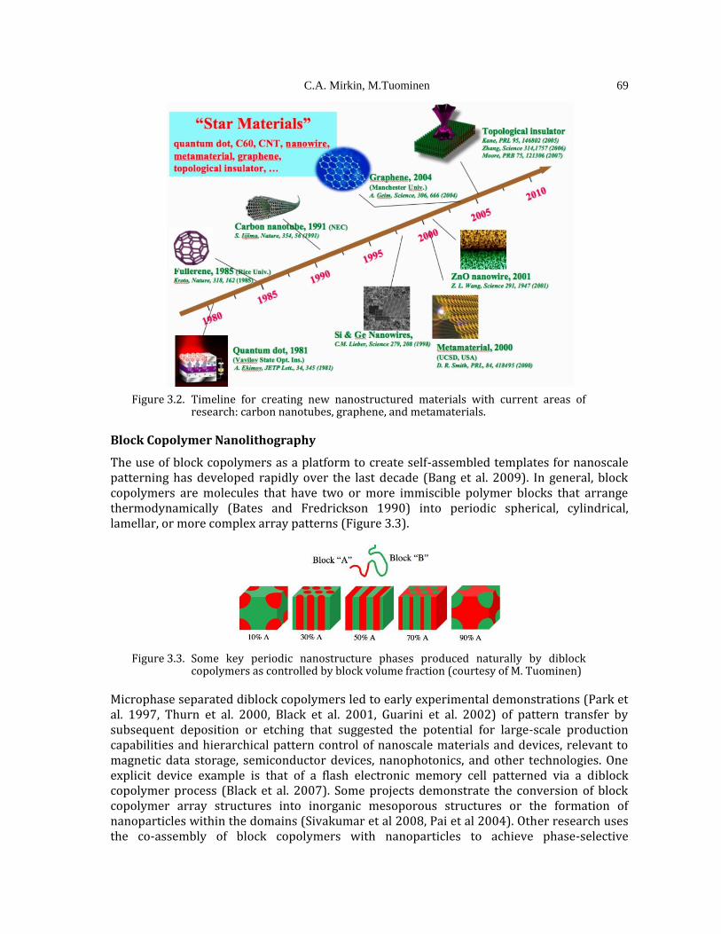
Figure 3.2 illustrates the timeline for several inorganic nanomaterials. Nanotechnology tools offer rapid approaches for making, screening, optimizing, and scaling potential catalysts for activity, selectivity, and environmental compatibility. In a single experiment, it would be possible to probe multiple questions that pertain to physical, chemical, mechanical, electrical, optical, or biological properties. High-throughput methods for screening nanocomposites relevant in a given photonic, electronic, or biomedical application will become increasingly important as science enables smaller feature dimensions with increased sensitivity.
C.A. Mirkin, M.Tuominen 69
Figure 3.2. Timeline for creating new nanostructured materials with current areas of research: carbon nanotubes, graphene, and metamaterials.
Block Copolymer Nanolithography
The use of block copolymers as a platform to create self-assembled templates for nanoscale patterning has developed rapidly over the last decade (Bang et al. 2009). In general, block copolymers are molecules that have two or more immiscible polymer blocks that arrange thermodynamically (Bates and Fredrickson 1990) into periodic spherical, cylindrical, lamellar, or more complex array patterns (Figure 3.3).
Figure 3.3. Some key periodic nanostructure phases produced naturally by diblock copolymers as controlled by block volume fraction (courtesy of M. Tuominen)
Microphase separated diblock copolymers led to early experimental demonstrations (Park et al. 1997, Thurn et al. 2000, Black et al. 2001, Guarini et al. 2002) of pattern transfer by subsequent deposition or etching that suggested the potential for large-scale production capabilities and hierarchical pattern control of nanoscale materials and devices, relevant to magnetic data storage, semiconductor devices, nanophotonics, and other technologies. One explicit device example is that of a flash electronic memory cell patterned via a diblock copolymer process (Black et al. 2007). Some projects demonstrate the conversion of block copolymer array structures into inorganic mesoporous structures or the formation of nanoparticles within the domains (Sivakumar et al 2008, Pai et al 2004). Other research uses the co-assembly of block copolymers with nanoparticles to achieve phase-selective

3. Synthesis, Processing, and Manufacturing of Components, Devices, and Systems
70
assembly/disassembly of nanoparticles in block copolymer thin films and produce nanotubes, hexapods, and other complex mesostructures by adjusting the relative size of nanoparticles (Warren et al. 2007a, b). Diblock copolymers serve as a popular motif for directed self-assembly in which fields or pre-patterned surface features can control the orientation, alignment, and long-range order of the nanoscale polymer domain arrays (Segalman, Yokoyama, and Kramer 2001, Black and Bezencenet 2004, Cheng, Mayes, and Ross 2004, Ruiz et al. 2008, Cheng et al. 2008, Bita et al 2008, Park et al. 2008). Cylindrical microdomains as small as 3 nm have been produced, along with orientational control methods that suggest routes for low-cost continuous roll-to-roll manufacturing (Park et. 2009). Recent work demonstrates the ability to use pre-patterned surfaces to coerce block copolymer assemblies into non-natural, somewhat arbitrary patterns more suitable for nanoelectronic devices—including square arrays, T-junctions, and bends (Wilmes et al 2006, Park et al. 2007, Tang et al. 2008, Chai and Buriak 2008, Jung et al. 2010, Yang et al. 2010) (Figure 3.4).
Figure 3.4. Four examples of nanostructure patterns fabricated by directed self-assembly using diblock copolymers (sources: upper left, Bita et al. 2008; upper right, Chai and Buriak 2008; lower left, Galatsis et al. 2010; lower right, Yang et al. 2010).
Quite clearly, the design rules for block copolymer nanolithography are rapidly becoming established and will continue to advance through this type of fundamental research. Multi-level alignment and 3D patterns are critical research targets for the future.
Scanning Probe-Based Lithography
Dip-Pen Nanolithography
Dip-pen nanolithography (DPN), polymer pen lithography (PPL), inkjet printing, transfer-printing techniques, and scanning probe block copolymer lithography over the past decade are illustrated in Figure 3.5. Such tools have enabled the controlled synthesis and placement of nanomaterials and nanostructures on a surface with a broad range of materials and substrate compatibility.

C.A. Mirkin, M.Tuominen 71
Figure 3.5. Timeline for scanning probe-based molecular printing tools such as dip-pen nanolithography (Braunschweig, Huo, and Mirkin 2009).
The ability to pattern surfaces with sub-100 nm resolution has been a driving force in nanotechnology fueled by the semiconductor industry’s desire to continually shrink the size of bulk materials, and by new capabilities for biological experiments made possible through high-density biomolecule arrays. In this respect, DPN (Braunschweig, Huo, and Mirkin 2009; Piner et al. 1999; Salaita, Wang, and Mirkin 2007) has become a commercial technique for direct-write molecular printing; it is capable of patterning surfaces with sub-50 nm feature size (Figure 3.6). As a patterning tool, many applications have been explored, and DPN has been used for fundamental transport studies (Rozhok, Piner, and Mirkin 2003; Giam, Wang, and Mirkin 2009), as a fabrication technique for photomasks (Jae-Won Jang 2009), and as a method of creating biological screening devices, including an assay for HIV virus p24 antigen in serum samples (Lee 2004).
Figure 3.6. (Left) Schematic of patterning alkanethiols on Au by DPN. (Right) Optical micrograph of 55,000 Si pen array; scale bar is 100 µm. (Inset) Scanning electron micrograph of the pens (from Salaita, Wang, and Mirkin 2007).
One-dimensional (1D) arrays of cantilevers have been fabricated to increase throughput by a factor equal to the number of tips in the array (Salaita et al. 2005; Minne et al. 1996). This idea of passive parallelization of DPN was further expanded to generate 2-dimensional (2D) arrays consisting of 55,000 tips capable of increasing throughput by as much as four orders
3. Synthesis, Processing, and Manufacturing of Components, Devices, and Systems
72
of magnitude with as many as 88 million dots fabricated in approximately 5 minutes (Figure 3.6; Salaita et al. 2006). To date, DPN arrays with as many as 1.3 million cantilevers have been fabricated. The massive parallelization of DPN opens up the possibility to fabricate combinatorial libraries of nanostructures with feature sizes two to three orders of magnitude smaller than current widely used microfabrication techniques such as photolithography, ink jet printing, and robotic spotting. The ability to shrink feature size to the nanoscale therefore allows researchers to print on the scale of biology. This feature size reduction not only increases the number of features per unit area but also allows single particle structures such as viruses and cells to be manipulated individually. Before combinatorial arrays generated by DPN become commonplace however, robust methods of inking and simultaneously transporting multiple different molecules to a substrate in multiplexed fashion must be developed.
A microfluidic inkwell platform capable of delivering multiple different inks to a 1D array of tips has been developed, allowing for the simultaneous deposition of up to eight different inks (Banerjee et al. 2005). This technique, however, is not capable of addressing a 2D array of tips for massively parallel multiplexed DPN. Toward this goal, an inkjet printing technique has been developed for massively multiplexed parallelization, whereby tips within 1D and 2D arrays are inked with chemically distinct inks (Wang et al. 2008). DPN may become in the next decade a general nanofabrication tool that combines high throughput, high resolution, and multiplexed deposition capabilities.
Polymer Pen Lithography
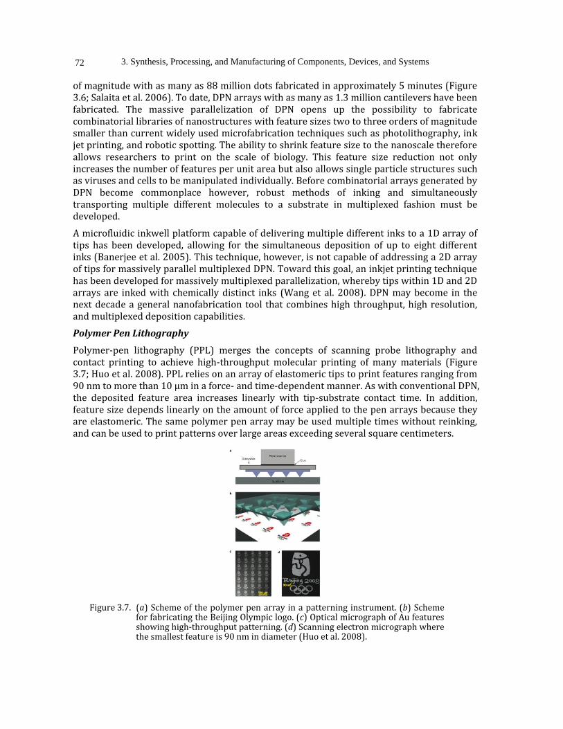
Polymer-pen lithography (PPL) merges the concepts of scanning probe lithography and contact printing to achieve high-throughput molecular printing of many materials (Figure 3.7; Huo et al. 2008). PPL relies on an array of elastomeric tips to print features ranging from 90 nm to more than 10 µm in a force- and time-dependent manner. As with conventional DPN, the deposited feature area increases linearly with tip-substrate contact time. In addition, feature size depends linearly on the amount of force applied to the pen arrays because they are elastomeric. The same polymer pen array may be used multiple times without reinking, and can be used to print patterns over large areas exceeding several square centimeters.
Figure 3.7. (a) Scheme of the polymer pen array in a patterning instrument. (b) Scheme for fabricating the Beijing Olympic logo. (c) Optical micrograph of Au features showing high-throughput patterning. (d) Scanning electron micrograph where the smallest feature is 90 nm in diameter (Huo et al. 2008).

C.A. Mirkin, M.Tuominen 73
The same materials that can be patterned in a DPN experiment are applicable to PPL—alkanethiols, polymers, and proteins—to name a few. To generate multiplexed patterns of several materials, it is possible to use the same masters that acted as the polymer pen molds and deposit ink in the pyramidal pits, much like an inkwell (Zheng et al. 2009).
Beam Pen Lithography
An extension of PPL termed beam pen lithography (BPL) uses the pen arrays to deliver light to a surface in a manner conventionally known as near-field scanning optical microscopy (Figure 3.8; Huo et al. 2010). The polymer pen arrays are coated with a thin opaque layer such as Au and then brought in contact with an adhesive poly(methyl methacrylate) surface to fabricate micrometer-sized apertures or by focused ion beam lithography to generate nanometer-sized apertures. Light can then be exposed to the backside of the pen arrays and channeled through the apertures to a photosensitive surface for fabricating subdiffraction-limited features in a high-throughput manner. This tool could enable researchers to rapidly design and produce novel devices and marks an additional capability enabled by scanning probe-based lithographies.
Figure 3.8. (a) Scheme of beam pen lithography. (b) Scanning electron micrograph of 100 nm features made using 400 nm light (Huo et al. 2010).
1D Systems
On-Wire Lithography
1D systems (e.g., nanowires and nanorods) represent an area of intense research interest. Like their 0-dimensional (0D) counterparts (e.g., nanoparticles and quantum dots), there are now a variety of methods for synthesizing such structures. However, by transitioning from 0D to 1D systems, the design space available to the researcher and ultimate user significantly increases (Ozin 2005). In addition to controlling the diameter, length, and composition of such structures, positive and negative architectural features can be introduced along the wire to realize structures with even greater functionality. In this regard, methods for nanowire fabrication and manipulation, analogous to the many powerful types of nanolithographies available to the materials researcher (e-beam lithography, nanoimprint lithography, and DPN), would be extremely useful.
On-wire lithography (OWL) is a powerful process that allows for the control of feature composition and size from the sub-5 nm to many micrometer length scales (Figure 3.9). In the OWL process, anodic aluminum oxide films (either purchased from commercial vendors or fabricated in the lab) are used as templates to electrochemically deposit nanowires. Cylindrical, aligned pores permeate these templates and serve as discrete regions for nanowire growth. Anodic aluminum oxide films are available, with pores ranging in diameter from 400 to 13 nm. Deposition of materials into these pores is made possible by first evaporating a metal backing onto one side of the alumina. This evaporated film acts as a

3. Synthesis, Processing, and Manufacturing of Components, Devices, and Systems
74
working electrode during wire synthesis. By electrochemically reducing metal ions from solution into the now half-closed pores of the template, nanowires can be grown with lengths and compositions corresponding to the applied current and metal ion precursor, respectively. Dissolution of the template and evaporated metal backing results in a suspension of billions of nanowires (Figure 3.9). This suspension is sprayed onto a glass slide, and a backing layer is deposited on the wires by chemical or physical deposition methods. Both conducting (metals) and insulating (SiO2) backing materials can be used. With the backing layer in place, wire segments can be selectively dissolved on the basis of differences in chemical reactivity. This approach allows nanometer-scale gaps, disks, and disk arrays with precise control over not only the size of the gap, but also the thickness, composition, and periodicity of the disks to be prepared.
Figure 3.9. The on-wire lithography (OWL) process (Qin et al. 2005).
OWL-Based Encoding Materials
Encoded materials are used for many applications, including cryptography, computation, brand protection, covert tracking of material goods and personnel, and labeling in biological and chemical diagnostics (Qin et al. 2006). The disk and gap structures made by OWL are particularly interesting for this class of materials because they are dispersible, allow for massive encoding on the basis of the length and location of individual chemical blocks within the structures, and can be easily functionalized using conventional surface chemistries. These properties of OWL-generated nanostructures have been used to create a library of optimized disk pair structures that vary in the number and position of the disk pairs along the silica backing (Qin et al. 2007). Each of these structures represents a unique nanodisk code label (Figure 3.10).
Figure 3.10. Structures made by OWL. (A) Disk arrays (adapted from Qin et al. 2006). (B) Zoomed out image demonstrating uniformity of rods (Qin et al. 2005). (B inset) 2.5-nm gap produced by means of OWL (Qin et al. 2007).
By functionalizing the disk pairs with an oligonucleotide capable of binding a target DNA followed by hybridization of a chromophore labeled “reporter” strand, particular

C.A. Mirkin, M.Tuominen 75
oligonucleotides can be captured and detected by means of hybridization to the structure. This sandwich assay design has been successfully implemented using the intensity of the Raman reporter as a measure of the concentration of the target to detect oligonucleotides with low pM sensitivity. These examples highlight the unique applications of OWL generated structures, which are made possible by the placement of SERS-active materials in a highly tailorable manner.
Test Bed for Molecular Electronics
In addition to plasmonic materials and SERS active substrates, the OWL process has been applied to synthesizing unique materials for understanding nanoscale transport phenomena (Chen et al. 2008). Molecular electronics is a promising route to extremely compact, high-speed computing and data storage systems that are beyond the limits of conventional, solid-state circuitry (Nitzan and Ratner 2003). Because OWL can be used to produce large quantities of high-quality nanowires with sub-5 nm gaps, it an ideal platform with which to study the charge transport properties of organic molecules that are designed to self-assemble across such gaps (Figure 3.11).
Figure 3.11. (A) SEM image of a device prepared with an OWL-fabricated wire having a 3-nm gap. (B) Representative I-V response for 3-nm OWL-fabricated gaps before being modified with OPE-1 (Pure nanogap line) and after (OPE line). (C) A diagram of OPE-1 molecules spanning the 3-nm gap (adapted from Chen et al. 2008).
DNA-Mediated Assembly of Gold Nanostructures
The ability to direct the placement of nanomaterials in 3 dimensions with a high degree of specificity and tailorability has been a goal of nanotechnology since its inception. By building complex nanostructures from the ground up with control over the lattice parameters, crystallographic symmetry, and material composition, it is thought that materials with new, emergent properties can be synthesized (Talapin et al. 2009; Nie, Petukhova, and Kumacheva 2010). Methods to arrive at an ordered nanocrystal superlattice typically rely on drying effects or layer-by-layer assembly methods (Shevchenko et al. 2006; Lin, Chen, and Gwo

3. Synthesis, Processing, and Manufacturing of Components, Devices, and Systems
76
2010). Although these techniques have been used to demonstrate an impressive degree of crystallographic order over large areas, they do not afford a particularly high level of control over the lattice parameters of the resulting superlattices and cannot assemble particles independent of their size. An especially attractive alternative involves the use of DNA as a programmable linker that serves to direct the assembly of nanostructures in 3 dimensions with extraordinary control over crystallographic parameters (Park et al. 2008). DNA is an ideal material for the creation of nanoscale architectures, because its self-recognition capabilities allow for the assembly of materials with properties that can be varied via judicious DNA design. When DNA “linkers” that have short, self-complementary sticky ends are hybridized to oligonucleotide functionalized gold nanoparticles and allowed to induce assembly, a face-centered cubic (FCC) superlattice is observed using small angle X-ray scattering (Figure 3.12). Likewise, when non-self-complementary DNA linkers are hybridized to oligonucleotide functionalized particles, a body-centered cubic (BCC) superlattice is observed.
This difference in crystal symmetry arises from the driving force for DNA-gold nanoparticle conjugates to maximize the number of hybridization interactions in a given arrangement. For example, nanoparticles in a 1-component system (i.e., self-complementary linkers) have the greatest number of interparticle connections in an FCC configuration. Similarly, nanoparticles in a 2-component system (i.e., non-self-complementary linkers) have the greatest number of favorable hybridization interactions in a BCC configuration. Simply by changing the number of nucleobases in the linker oligonucleotides, scientists can systematically control the interparticle spacing of the resulting colloidal crystals anywhere from ~20 to ~55 nm (Hill et al. 2008). Interestingly, these colloidal crystals initially assemble into a disordered aggregate that subsequently undergoes a reorganization process ultimately resulting in an ordered superlattice (Macfarlane et al. 2009).
Figure 3.12. Schematic illustration of the DNA-mediated assembly of gold nanoparticles. DNA linkers with short recognition sequences are hybridized to oligonucleotide functionalized gold nanoparticles. The sequence of the overhanging recognition unit dictates the assembly into FCC or BCC superlattices (adapted from S.Y. Park et al. 2008).
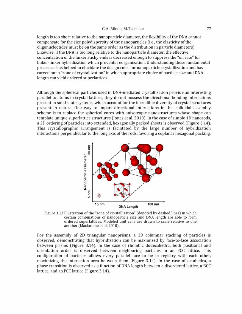
One clear difference between solid-state atomic assembly and DNA-mediated nanoparticle assembly is the ability to control the properties of a nanostructure by changing its size, independent of its crystallographic arrangement. When oligonucleotide-functionalized gold nanoparticles of different sizes are used in the assembly process, a fascinating trend emerges in which only certain combinations of nanoparticle diameter and DNA length are able to reorganize into an ordered superlattice (Figure 3.13; Macfarlane et al. 2010). When the DNA
C.A. Mirkin, M.Tuominen 77
length is too short relative to the nanoparticle diameter, the flexibility of the DNA cannot compensate for the size polydispersity of the nanoparticles (i.e., the elasticity of the oligonucleotides must be on the same order as the distribution in particle diameters). Likewise, if the DNA is too long relative to the nanoparticle diameter, the effective concentration of the linker sticky ends is decreased enough to suppress the “on rate” for linker-linker hybridization which prevents reorganization. Understanding these fundamental processes has helped to elucidate the design rules for nanoparticle crystallization and has carved out a “zone of crystallization” in which appropriate choice of particle size and DNA length can yield ordered superlattices.
Although the spherical particles used in DNA-mediated crystallization provide an interesting parallel to atoms in crystal lattices, they do not possess the directional bonding interactions present in solid-state systems, which account for the incredible diversity of crystal structures present in nature. One way to impart directional interactions in this colloidal assembly scheme is to replace the spherical cores with anisotropic nanostructures whose shape can template unique superlattice structures (Jones et al. 2010). In the case of simple 1D nanorods, a 2D ordering of particles into extended, hexagonally packed sheets is observed (Figure 3.14). This crystallographic arrangement is facilitated by the large number of hybridization interactions perpendicular to the long axis of the rods, favoring a coplanar hexagonal packing.
Figure 3.13 Illustration of the “zone of crystallization” (denoted by dashed lines) in which certain combinations of nanoparticle size and DNA length are able to form ordered superlattices. Modeled unit cells are drawn to scale relative to one another (Macfarlane et al. 2010).
For the assembly of 2D triangular nanoprisms, a 1D columnar stacking of particles is observed, demonstrating that hybridization can be maximized by face-to-face association between prisms (Figure 3.14). In the case of rhombic dodecahedra, both positional and orientation order is observed between neighboring particles in an FCC lattice. This configuration of particles allows every parallel face to be in registry with each other, maximizing the interaction area between them (Figure 3.14). In the case of octahedra, a phase transition is observed as a function of DNA length between a disordered lattice, a BCC lattice, and an FCC lattice (Figure 3.14).

3. Synthesis, Processing, and Manufacturing of Components, Devices, and Systems
78
3.3 GOALS FOR THE NEXT 5–10 YEARS: BARRIERS AND SOLUTIONS
In the coming decade, synthesis work should endeavor to link itself with research on scale-up and advanced processing, in addition to the research that enables precise control of nanomaterial shape, structure, composition, and crystal facet. There is an enormous untapped potential in this area. The implementation of processes based on inherently scalable scientific phenomena, such as self-assembly, directed assembly, and bioinspired synthesis, will lower manufacturing costs and broaden the applicability of nanomaterials. Combined with a new generation of automation and manufacturing design optimization, advancements over the next 10 years have the potential to usher in a new age of sustainable manufacturing. Emphasis should be placed on the manufacturing science and engineering, which requires close cooperative efforts among industry, academia, and government. The section that follows discusses specific opportunities for nanofabrication, barriers to success, and proposed solutions to overcome the challenges and reach these goals.
Figure 3.14. Models of superlattices derived from DNA-mediated assembly of anisotropic nanostructures. (A) 2D hexagonal arrangement of nanorods. (B) 1D columnar ordering of triangular nanoprisms. (C) Face-centered cubic ordering of rhombic dodecahedra. (D) Illustration of the transition from disordered to BCC to FCC ordering with increasing linker length in the assembly of octahedra (Jones et al. 2010).
Nanopatterning Tools
Within the next 10 years, researchers are expected to achieve two- and three-dimensional macroscopic materials control, with the ability to dictate where building blocks are placed down to 1-nm resolution, especially in the context of nanoprinting capabilities. Currently, there are no suitable methods with appropriate resolution and general materials compatibility. Moreover, it is challenging to maintain a narrow distribution in defect sizes. In this regard, the convergence of top-down and bottom-up chemistry or directed assembly approaches may enable high-resolution synthesis and control of nanoscale architectures. Such enabling work will require a shift in the emphasis from fundamental research to manufacturing in nanotechnology, which currently suffers from insufficient collaboration between academia and industry. Specifically, the scale-up of nanomaterials synthesis is disconnected from fabrication and manufacturing at the industrial scale level. Further financial incentives for industry leaders to engage and partner with academia will foster united efforts that address the challenges in nanomanufacturing science. Industry, academic, and government partnerships will enable all parties to run and assess pilot projects and manufacturing test beds. In such work, they must take laboratory benchtop proof-of-concept

C.A. Mirkin, M.Tuominen 79
methods and develop approaches that address commercially relevant production volumes. This goal can be realized through developments in science, metrology, test data, tooling, and materials.
Plasmonic Metamaterials
Within the emerging field of plasmonic metamaterials, there are no accurate structure-property relationships or design rules due to the lack of complete scientific understanding for these systems. Experiments and data specifically geared toward obtaining accurate first principles scientific understanding of structure and resulting properties will be enabling for model predictions and property customization. Improved theoretical algorithms and better nanomanufacturing could allow researchers to tailor the optical properties of oriented metallic superstructures. These metamaterials could then be used in optoelectronic applications as light harvesting systems and, more specifically, affect the performance to cost ratio for energy conversion, storage, transmission, and efficiency.
Combinatorial Chemistry
Currently, high-sensitivity, high-throughput assays are only in development, even though many scientific fields could greatly benefit from rapid ways for making, screening, optimizing, and scaling nanoscale materials ranging from biological targets to catalysts for their activity, selectivity, and environmental compatibility. Clever combinatorial approaches will be needed to enable rapid screening of materials. In the context of nanoparticle catalysts, there needs to be greater nanoparticle design control, including shape, valency, composition, and other factors that provide recipes for designer functionality. It is important to establish design rules for multiscale synthesis and integration of nanoscale systems to assemble these particles into hierarchical structures.
Transition from Silicon- to Carbon-Based Devices
There are currently infrastructure barriers to growth for the transition from the silicon age to the carbon age for integrated electronic and photonic devices. Lower cost methods for making and integrating device components and taking advantage of component structural flexibility will help realize carbon-based devices. At the same time, it is important to realize the potential of silicon beyond electronics. It may be possible to use nanoscale silicon structures in the fields of photonics, catalysis, biotechnology, and energy applications. This work will involve the synthesis and purification of components, chemical stability (e.g., avoiding oxidation), and sometimes component integration.
Bioinspired and Biomimetic Devices
For the integration of biomolecules into functional bioinspired or biomimetic devices, it is important to synthesize, purify, and scale up these nano-based instruments and therapeutics to meet regulatory agency requirements. To do so, there should be reduced heterogeneity of nanostructures and improved understanding and engineering of biomolecules on nanostructured surfaces. Furthermore, it will be critical to establish an effective biomolecule-electronic interface, although currently there is an incomplete understanding of molecule-level interactions. As with nanopatterning tools, the convergence of top-down and bottom-up chemistry and directed assembly approaches are promising for this challenge. Advancing organic-inorganic nanomaterial hybrids will also require appropriate processing methods that preserve the properties of the organic component.

3. Synthesis, Processing, and Manufacturing of Components, Devices, and Systems
80
Nanomanufacturing Capabilities
The lack of the ability to introduce nanoscale discoveries in manufacturing, economically, with repeatability, and with full in situ instrumentation to monitor the processes, is a barrier that must be addressed in the future.
Nanomaterials in the Forest Products Industry
The forest products nanotechnology roadmap (www.nanotechforest.org) identifies the industry vision as “sustainably meeting the needs of present and future generations for wood-based materials and products by applying nanotechnology science and engineering to efficiently and effectively capture the entire range of values that wood-based lignocellulosic materials are capable of providing.” The industry vision is well aligned with society’s need for establishing a source of sustainable materials and products. Priority areas for nanotechnology in the forest product industry are: improving the strength-to-weight performance; liberating and using nanocellulose and nanofibrils naturally present in wood; and achieving a better understanding of water-lignocellulosic interactions with the aim of improving the dimensional stability and durability of wood-derived products.
3.4 SCIENTIFIC AND TECHNOLOGICAL INFRASTRUCTURE NEEDS
Synthesis and manufacturing in nanotechnology has demanding infrastructure needs. Although some of the new nanofabrication and synthesis processes can be inherently inexpensive, their characterization is not. As processes make their way from the laboratory to the production plant, the demand on metrology is even greater, because characterization speed and throughput is often an issue. The cost of the production toolset increases as well, because high volume and high speed are often requirements. Successfully responding to the following infrastructure needs will help accelerate nanotechnology research and development:
In situ or online characterization facilities for synthesizing and manufacturing high precision, high purity nanomaterials and nanostructures
Greater availability of large scale expensive fabrication, characterization, and measurement facilities (e.g., electron-beam lithography, clean room foundries, synchrotron sources, neutron sources)
Extensive integration of interdisciplinary research and activities for technological breakthrough and transition of nanoscience to practical products
Development of nanomanufacturing education curricula as an integral part of such activities, with a strong emphasis on innovation education and manufacturing engineering principles
National nanomanufacturing development roadmap, jointly developed by industry, academia, and government stakeholders
Long-term strategic research focus on basic nanotechnology research
Adequate national facilities for rapid and inexpensive screening of new nanomaterials for environmental health and safety impact
A broader portfolio of standard reference nanomaterials for instrument and tool calibration
Accessible databases and libraries with information on nanomaterial properties, nanomanufacturing process information, and safety

C.A. Mirkin, M.Tuominen 81
3.5 RESEARCH AND DEVELOPMENT INVESTMENT AND IMPLEMENTATION STRATEGIES
The United States must continue a strong base of fundamental research in nanotechnology but at the same time significantly increase activities in nanomanufacturing, product engineering, and innovation education. This combination serves best to generate societal and economic benefits via several main points:
Foster collaboration among industry, universities, and research institutes. These relationships provide cost sharing, avoid redundant efforts, generate more effective facility use, and facilitate a more rapid commercialization. Efforts should be made to ensure that both large corporations and small start-up companies participate and benefit.
Promote and fund a set of complementary regional clusters that work to accelerate nanotechnology development and commercialization. Each cluster should have a relatively narrow thematic focus as a genuine national center of excellence.
Promote interdisciplinary work. Specifically, the challenges facing medicine need direct involvement of engineers, scientists, and clinicians.
Build a robust value chain from raw materials to nanocomponents to final products. Fill weaknesses and gaps in the nanotechnology value chain to enable promising applications to grow and thrive. Strengthen the U.S. National Nanomanufacturing Network.
Develop training programs and nanomanufacturing education curriculum. Increase investment in people who are trained in developing new analytical techniques. Such efforts can include postgraduate courses in nanoscience and nanotechnology and long-term positions for researchers. Promote multidisciplinary and integrative research.
Increase fundamental research funding to generate new knowledge of phenomena and manipulation of matter at the nanoscale.
Provide more investment in nanotoxicology to evaluate the safety of nanomaterials.
3.6 CONCLUSIONS AND PRIORITIES
In the coming decade, the research and development community must complement its ongoing fundamental research activities in synthesis, assembly, and processing by placing a stronger emphasis on the development of nanomanufacturing science and engineering. Nanomanufacturing (science based, reproducible, sustainable, and cost-effective) needs to be developed in conjunction with other areas such as nanobiotechnology and nanomedicine (e.g., diagnostics, drug delivery, and disease treatment), energy applications (e.g., conversion, storage, transmission, and efficiency), environmental fields (e.g., sensors, remediation, water purification), informatics (e.g., providing data, models, and information needed for efficient design, testing, development, and manufacturing), electronics (based on new architectures that specifically utilize the intrinsic properties and geometries of nanomaterials), and educational challenges (e.g., promoting the value of nanoscience and nanoengineering degrees; addressing lack of textbooks, emphasizing community college, undergraduate, and graduate education; and integrating partnerships with industry).
The following priorities have been identified for the next decade:
Creating nanomaterials and systems “by design” is a main goal. Integration of fundamental research, modeling, simulation, processing, and manufacturing in a continuing R&D approach is essential.
Development of a library of nanostructures (particles, wire, tubes, sheets, modular assemblies) of various compositions with industrial-scale quantities

3. Synthesis, Processing, and Manufacturing of Components, Devices, and Systems
82
Investigation of new processes for large scale environmentally benign manufacturing of graphene and plasmonics materials
Fundamental understanding of the pathways for self-assembly or controllable assembly of atoms or molecules into larger and stable nanostructures. Nanobio-manufacturing will expand to new approaches.
Emulation of proven natural designs in nanosystem manufacturable architectures
Scalable manufacturing processes using three-dimensional programmable assembly will be realized. Several “killer applications” are expected to emerge.
Support manufacturing of large and flexible displays for mass use.
Develop ability to print features over large areas exceeding many square centimeters with sub-10 nm resolution is needed in electronics and photonics. Materials flexibility for both hard and soft matter will require the integration of various strategies. The purpose is that nano-imprinting will be low-cost and in mass production. AFM lithography should be developed toward manufacturing use.
Life-cycle environmentally-friendly nanomanufacturing technologies will increase as required by market.
Develop nanoinformatics for nanomaterials and nanoscale devices.
3.7 BROADER IMPLICATIONS OF NANOTECHNOLOGY RESEARCH AND DEVELOPMENT ON SOCIETY
Synthesis and manufacturing are essential steps to be addressed for economical application of nanotechnology for societal needs as described in more detail in Chapter 13. Nanotechnology has the potential to benefit society in numerous areas from cosmetics to cars and from electricity to medicines. This impact can be readily seen with biomedical devices (e.g., diagnostics, drug delivery), electronic devices (e.g., mobile communication systems, portable data devices), efficient energy technologies (e.g., generation, conversion, transmission, and storage), and food industry products (e.g., production, packaging, safety) as they are translated from biology, chemistry, engineering, and materials science.
3.8 EXAMPLES OF ACHIEVEMENTS AND PARADIGM SHIFTS
3.8.1 Discovery of graphene (see also Chapter 8)
Contact person: Mark Tuominen, University of Massachusetts, Amherst
Hand-in-hand with explorations of material properties have existed efforts to synthesize them in a cost-effective, commercially relevant fashion. A good case study is the carbon nanomaterial, graphene—a single atomic layer of graphite. Originating with a process (Novoselov et al. 2004) that could not easily be scaled up (mechanical rubbing off a layer of graphite), graphene was produced so that its properties could be tested. Very quickly, the scientific community discovered that graphene has excellent electrical properties (Geim and Novoselov 2007) that could be used in a variety of ways, including transistors and transparent conducting electrodes. Indeed, this excitement was ratified by the 2010 Nobel Prize in physics being awarded for the discovery of graphene. The exceptional properties of graphene drove the research community to develop new, commercially viable methods to produce graphene. Indeed, the International Technology Roadmap for Semiconductors added graphene and carbon nanotubes to the roadmap (Figure 3.15).

C.A. Mirkin, M.Tuominen 83
Figure 3.15. Schedule for carbon nanoelectronics from the 2009 International Technology Roadmap for Semiconductors.
Huge strides have been accomplished within the last 2 years in large-area (Li et al. 2009), roll-to-roll production of graphene, and it has now been demonstrated for use as a transparent conducting electrode in prototype displays (Figure 3.16; Bae et al. 2010). This is only one representative application, but one that solves a pressing issue: replacement of indium tin oxide as a transparent electrode when indium reserves are rapidly depleting. Many other uses for nanoscale carbon can be expected over the next decade.
Figure 3.16. Images of large scale production of graphene grown on copper foils and transferred to a polymer layer for use in large area display applications (from Li et al. 2009 and Bae et al. 2010).

3. Synthesis, Processing, and Manufacturing of Components, Devices, and Systems
84
3.8.2 The Opportunity for Atomically Precise Manufacturing
Contact person: John N. Randall, Zyvex Labs
Improved manufacturing precision is a proven path to increasing the efficiency, quality, and reliability of existing products. It is also a key enabler in developing new products and applications. As manufacturing precision approaches the atomic and molecular scale, researchers have the unique opportunity to exploit the quantized nature of matter and make precision absolute. For the first time, the possibility of making nanoscale objects that are not just similar but are in fact exact copies is within reach.
Zyvex Labs has a project to develop an atomically precise manufacturing technology (Randall et al. 2010). The technical approach is an integration of two known experimental techniques: H depassivation lithography from Si (100) surfaces (Randall et al. 2009) with a scanning tunneling microscope (STM) and silicon atomic layer epitaxy (Suda, Hosoya, and Miki 2003) using disilane or other Si-H precursor gases to deposit Si where H has been removed (Figure 3.17). This pattern and deposit cycle is repeated in ultra high vacuum to control the creation of 3D structures.
Figure 3.17. (Left) H (white) atoms removed from Si (blue) surface by electron stimulated desorption by STM. (Middle) Si-H precursor gas selectively deposits on passivated Si where H has been removed (middle). (Right) Patterning process is repeated with another deposition cycle to create 3D structures.
This digital fabrication process exploits the discrete nature of matter. Several key features differentiate this process from typical scanning probe manipulation of matter: The tip never contacts anything; the H atoms are removed into the gas phase; and the deposited material arrives from the gas phase. Although this fabrication process has not been demonstrated with atomic (absolute) precision, perfect patterning has. The principal challenge is demonstrating good quality epitaxy below 300°C that maintains atomic precision while creating 3D structures. The experimental results suggest that epitaxial growth is possible at 220°C where H mobility on Si surfaces is still very slow. The project also includes monolayer passivation of Si surfaces, improved STM tip technology, and MEMS (Micro electro mechanical systems) closed loop nanoscanners. This approach will enable applications for processes requiring only an extremely small volume of material. It has been calculated, using a full cost of ownership model, that the cost of production would be approximately $2,100/μm3. Many applications would be cost-effective even at this price point. Among these applications are nanopores for DNA sequencing, metrology standards, templates for nanoimprint lithography, nano electromechanical resonators for extremely low power radios, and Kane Qubit’s for quantum computing. In the long term, with the sort of exponential increase in performance/cost seen in other technologies, and because this fabrication technology will be adaptable to many other material systems (semiconductors, metals, and insulators), it could become the foundry that enables widespread, cost-effective nano-manufacturing. Initial

C.A. Mirkin, M.Tuominen 85
estimates predict that by 2020, Zyvex Lab consortium members will develop 7 to 9 key new technologies using this platform with a market valuation of $7 to $600 million.
3.8.3 Dendrimers: 2010–2020
Contact person: Donald A. Tomalia, Central Michigan University
Dendrimer structures and processes (2000–2010). Dendrimers are synthetic core-shell, soft matter nanobuilding blocks that are recognized as members of the fourth major class of macromolecular architecture after linear, crosslinked, and branched polymers. They are derived from 2 or more dendrons attached to a common core. Architecturally, they possess onion-like topology that consists of a core, an interior (e.g., shells or generations), and terminal groups (e.g., surface chemistry).
They are synthesized by two major “bottom-up” strategies; namely: covalent divergent and covalent convergent syntheses (Tomalia and Fréchet 2001; Figure 3.18). These pre-2000 processes produced precise nanostructure controlled dendrimers as a function of size, shape, surface chemistry, and flexibility/rigidity that rival structural regulation normally observed for biological nanoparticles such as proteins, DNA, and RNA (Tomalia 2004). In the last decade, substantial progress has occurred for covalent dendrimer synthesis on the basis of Sharpless-type “click chemistry.” These covalent processes have produced more than 100 different dendrimer interior compositions and nearly 1,000 differentiated surface chemistries. More recently, a new class of “supramolecular dendrimers” has emerged based on self-assembly processes pioneered by Percec and colleagues (Figure 3.19) involving amphiphilic dendrons (Peterca et al. 2008).
Figure 3.18. Enhancement of nanostructure complexity for commercialized dendrimer-
based products (2000–2010; Columns I–IV) and predicted future developments (Column V; 2010–2020).

3. Synthesis, Processing, and Manufacturing of Components, Devices, and Systems
86
Amphiphilic dendrons may be designed as a function of critical nanoscale design parameters such as size, shape, and surface chemistry to produce hollow/solid spherical dendrimers, as well as cylindrical-type dendrimers. These self-assembly principles/patterns have led to the first examples of Mendeleev-like nanoperiodic tables (Rosen et al. 2009). Such tables allowed a priori predictions of expected supramolecular dendrimer type with 85% to 90% accuracy based on a nanoperiodic concept reported by Tomalia (2009, 2010). The current production cost limits the applications to high added value products.
Dendrimer applications/products (2000–2010). Dendrimer-based commercial products were first introduced in the late 1990s. Pre-2000 dendrimer commercial activity focused on the development of simple dendrimer compositions as a function of their nanoscale size and surface chemistry (Tomalia 2010; Marx 2008). The first products to emerge in 2000–2010 are described as follows (Figure 3.18):
Column I: (a) organic light emitting diodes (Cambridge Display/Sumitomo, Japan), (b) DNA gene vectors (e.g., Superfect®; Qiagen, Germany), and (c) antiviral topical nanopharma (e.g., VivaGel®; Starpharma, Australia). VivaGel® is presently in Phase IIa, FDA-based clinical trials.
Column II: (a) magnetic resonance imaging agents (e.g., Gadomer-17®; Bayer/Schering Pharma AG, Germany), (b) siRNA delivery vector (e.g., Priofect, EMD and Merck), and (c) cardiac-diagnostics (e.g., Stratus; Siemens, Germany).
Column III: (a) protein detection amplifiers (e.g., UltraAmpTM, Affymetrix/Genisphere, Inc.), (b) ocular/surgical adhesives (e.g., DendriLens/OcuSeal; HyperBranch Medical Technology, Inc.), (c) and metal encapsulated/metal ligated dendrimer catalysts. More complex dendrimer-based nanodevices,
Column IV a–c are focused on critical nanomedicine applications that include (a) targeted delivery of cancer therapies, (b) targeted delivery of cancer therapies with concurrent imaging capability and (c) advanced polyvalent nanopharmaceutical prototypes referred to as G-protein-coupled receptor (GPCR) drugs, all of which are currently under development (e.g., National Institutes of Health and private sector) but not at a commercial stage (Menjoge, Kannan, and Tomalia 2010).
Present market sizes/values for dendrimer-based biological/nanomedicine commercial applications are estimated to be more than $100 million/year. Large markets exceeding $1 billion/year are expected to emerge in the near term pending the final FDA approval of dendrimer-based topical, antiviral pharmaceuticals (e.g., VivaGel). These dendrimer-based microbicide agents are active against HIV, genital herpes, and human papillomaviruses and have been granted fast track status by the FDA. Essentially all critical behavior-influencing specific dendrimer applications and commercial products are based on intrinsic nanoscale properties associated with this broad architectural category of quantized building blocks (Tomalia 2010). These features distinguish dendrimer/dendron building blocks as one of the unique and dominant nanoscale platforms that allow systematic CNDP engineering/design for future applications and commercialization.
The Future (2010–2020). Activities expected to emerge in the next decade will focus on products of value to a variety of social, health, and economic areas. More efficient dendrimer processes (i.e., high atom efficiencies, lower recycle and byproducts; Column V) will allow larger volume value markets outside of the medical field: (a) manufacturing (additives for enhancing productivity, quality, or properties of commodity goods); (b) food production (agricultural products for enhanced crop production, controlled deliveries of herbicides, pesticides, and fertilizers); (c) environmental remediation (clean water and air, sequestering

C.A. Mirkin, M.Tuominen 87
radioactive materials); (d) alternative energy (conversion and storage); (e) electronics [computing miniaturization, memory devices, illumination/displays (organic light-emitting diodes)]; and (f) miscellaneous (e.g., personal care products, antiaging, sensors, diagnostics, jet ink printing).
Completely new dendrimer/dendron structural designs (i.e., Janus dendrons/supramolecular dendrimers; Column V) will emerge based on “click chemistry” synthesis, poly(peptide) dendrimer constructions, region-specific dendrimer surface functionalizations, megamer (i.e., poly(dendrimer) synthesis and dendrimer-based covalent/self-assembly hybridizations with other well-defined hard/soft nano building blocks to produce unprecedented new nanocompounds and assemblies. Several examples include, advanced dendrimer-based polyvalent nanopharma (Column V) in areas such as antimicrobials, anti-inflammatories, and GPCR drugs, and so forth, as well as dendrimer-based drug delivery vectors/excipients and advanced delivery targeting/strategies (Column V). These dendrimer-based vectors are designed to guide/target genetic or small molecule therapies to specific disease sites (e.g., cancer, diabetes) with minimal collateral damage to healthy tissue. They will be selected and synthesized based on the implementation of combinatorial libraries/techniques much as is used for traditional small molecule pharmaceutical screening (Lee et al. 2005).
3.8.4 Dendrimersomes
Contact person: Virgil Percec, University of Pennsylvania
Tiny bubbles and other nanostructures that form spontaneously when highly branched bifunctional compounds are put in water have been discovered and characterized (Figure 3.19). The nanostructures may be more broadly useful for delivering drugs and other substances than similar nanostructures made from phospholipids or polymers. Researchers at the University of Pennsylvania reported in Science that a new family of vesicles, tubes, disks, and other shapes—which they call “dendrimersomes”—self-assemble from Janus dendrimers in water (Beguin and Frackowiak 2009). Dendrimersomes can act as hosts for a variety of guest molecules and could, therefore, have widespread applications as delivery vehicles for drugs, genes, imaging compounds, diagnostic agents, cosmetics, and other substances. Liposomes and polymersomes—synthetic vesicles made from phospholipids and polymers, respectively—have similar uses as delivery vehicles but several drawbacks: liposomes tend to be unstable and have short lifetimes, polymersome membranes are too thick to accommodate biological receptor and pore-forming proteins, and both liposomes and polymersomes adopt a wide range of sizes when they form and are difficult to derivatize. Dendrimersomes are stable for longer periods of time, are highly uniform in size, have the proper dimensions to accommodate membrane-spanning proteins, and are easily functionalized.
Figure 3.19. (Left) Janus dendrimers are amphiphilic, with nonpolar (left side) and polar (right) ends. (Right) Nanostructure dendrimersome cross-section shows its cell-membrane-like bilayer (Percec et al. 2010).

3. Synthesis, Processing, and Manufacturing of Components, Devices, and Systems
88
3.8.5 New Paradigms in Nanoceramics
Contact person: Lynnette D. Madsen, National Science Foundation
Key breakthroughs in nanoscale ceramics in the last decade include the following: nanoporous materials and structures, strain-engineered complex oxides, and inorganic nanotubes and related materials.
Nanoporous materials and structures. Research has focused on nanoporous materials with tunable pore sizes and porous structures. Application areas are wide ranging, including capacitive energy storage, hydrogen storage, methane storage, gas separation, sorption of biomolecules, water desalination, and porous electrode materials for electrical energy applications.
Carbide-derived carbons (CDCs) produced by extraction of metals or metalloids from metal carbides have shown promise (Beguin and Frackowiak 2009). The method allows the synthesis of most known carbon structures. Further, CDC formation can be controlled to produce highly porous carbon materials with superior tribological properties. Precise control of porosity is required to maximize the material performance (Figure 3.20). Research on the fundamental mechanisms governing the adsorption of cytokines by carbon materials could provide further insight and has the potential to save lives of people suffering from autoimmune diseases, severe sepsis, and multiple organ failure (Yachamaneni et al. 2010).
Researchers also focused on exploring predictive ways to synthesize closed-pore materials based on the use of surfactant micelles as templates to generate well-defined pore arrays. Surfactant templating has revolutionized the synthesis of nanoporous materials. Extending the scope of this powerful approach on new material compositions and on achieving more beneficial structural properties of the closed-pore materials is needed (Kruk and Hui 2008).
Figure 3.20. Normalized capacitance change versus the pore size of the carbide-derived carbon samples tested in an ionic liquid electrolyte. Normalized capacitance is obtained by dividing the gravimetric capacitance by the specific surface area. HyperChem models of the structure of ethyl-methylimmidazolium (EMI) and bis(trifluoro-methane-sulfonyl)imide (TFSI) ions show a size correlation (Largeot et al. 2008).
Similarly, electrically conducting zeolite-like or zeoate frameworks were targeted for improved electrical energy storage (Soghomonian and Heremans 2009). Some zeoate materials combine the properties of the well-known, but electrically insulating, microporous zeolites with an electronically active framework (Figure 3.21). Based on fundamental science,

C.A. Mirkin, M.Tuominen 89
novel energy storage and conversion mechanisms can be predicted and designed into new materials for many electrical energy applications from transportation to power-consuming electronics.
Figure 3.21. (Left) Zeoate framework structure with [(As6VIV12VV3O51) – 9Z] ∞ composition, where vanadium is blue, arsenic is yellow, and oxygen is red. The material crystallizes in a cubic space group with cell edge of 1,600 pm. (Middle) Plot of measured conductivities as a function of temperature (data from Soghomonian and Heremans 2009). (Right) Scanning electron micrograph of zeoate material from left panel; scale bar is 50 µm (courtesy of V. Soghomonian, Virginia Polytechnic Institute and State University).
Atomic-scale engineering of ferroelectric and related materials. Strain has been used in epitaxial thin-film structures to induce or enhance ferroelectricity (Haeni et al. 2004; Choi et al. 2004; Schlom et al. 2007). For example, ferroelectric capability was added to strontium titanate, SrTiO3, to provide the first ferroelectric directly on silicon (Warusawithana et al. 2009; Figure 3.22). This ferroelectric material may eliminate the time-consuming booting and rebooting of computer operating systems and prevent losses from power outages.
Figure 3.22. (Left) The arrangement between atoms of a film of strontium titanate and single crystal of silicon on which it was made. When sufficiently thin, strontium titanate can be strained to match the atom spacing of the underlying silicon and becomes ferroelectric. (Right) The schematic at the left has been written into such a film using the ability of a ferroelectric to store data in the form of a reorientable electric polarization (courtesy of J. Levy, University of Pittsburgh).
Using the same principles, a new ferroelectric ferromagnet has been synthesized based on europium titanate (EuTiO3) with a spontaneous magnetization × spontaneous polarization product at 4°K that is more than 100 times higher than any other known material (Lee et al. 2010). First principles calculations were used to design a strong ferroelectric ferromagnet by
3. Synthesis, Processing, and Manufacturing of Components, Devices, and Systems
90
exploiting strain in combination with spin-phonon coupling. These results open the door to higher temperature embodiments of strong ferromagnetic ferroelectrics, which would enable dramatic improvements in numerous devices, including magnetic sensors, energy harvesting, high-density multistate memory elements, wireless powering of miniature systems, and tunable microwave filters, delay lines, phase shifters, and resonators.
These and other advances have uncovered spectacular phenomena of fundamental scientific interest at oxide interfaces: self-generated ultrathin magnetic layers, orbitally reordered electronic systems, and conducting electron gases that can be patterned into nano-sized transistors (Mannhart and Schlom 2010). In most cases, full implementation is impeded by several factors. Examples include room-temperature mobilities that are orders of magnitude below useful values. Limitations on mobilities could be caused by sample quality as a result of defects such as cation nonstoichiometries, oxygen defects, intermixing, and nonhomogeneities. An improved control and understanding of defects is necessary for significant advances in the fabrication of individual films as well as superlattice stacks containing several conducting interfaces that can be locally interconnected. Structures may include other functional oxide materials, such as ferroelectrics or strongly correlated materials. Samples that contain many tunable interfaces in parallel will demand and enable new transport studies. Other considerations in terms of moving toward devices are cost efficiency of fabrication and compatibility with existing semiconductor fabrication processes. In the long run, the possibility exists to create new artificial materials in bulk form. As Mannhart and Schlom (2010) explained, “The theoretical modeling of interfaces in correlated systems is another area ripe with opportunity. This is a gold mine begging for materials-by-design solutions using the full arsenal of simulation, modeling, and theory.”
Inorganic nanotubes. Inorganic nanotubes, such as nitride, sulfide, and oxide nanotubes, have the potential to be used for high-load, high-temperature, and high-pressure applications (Chen, Elabd, and Palmese 2007). TiO2 nanotubes have a role in photovoltaics, water purification, and CO2 sequestration. Boron nitride nanotubes were predicted (Rubio, Corkill, and Cohen 1994) and subsequently synthesized (Zettl 1996). Their energy gap is independent of wall number, diameter, or chirality and thus they constitute desirable insulating structures for geometrically and electronically confining atomic, molecular, or nanocrystalline species (Blase et al. 1994). In addition, boron–carbon–nitrogen systems have potential in terms of nanotubes and in other configurations (Ci et al. 2010). Key factors in the development of various nanotubes seem to be (a) efficient and effective synthesis methods, (b) control of crystallinity and specific properties, (c) dispersion of nanotubes, and (d) the creation of composite materials with strong bridges between the different materials (Golberg et al. 2007). There are also opportunities in creating complex, hybrid (multicomponent) nanowires and nanotubes to build multifunctional nanomaterials. In the next decade, the creation of complex architectures with multiple nanoscale components assembled in a hierarchical fashion is likely.
3.8.7 Advanced Carbon Wiring
Contact person: Rick Ridgley, National Reconnaissance Office
The need for advanced wiring concepts can minimize ohmic losses and signal noise. The aerospace industry is constantly interested in reducing inactive spacecraft mass as a way to save payload costs and increase hardware efficiency. In general, the wire harness mass is approximately 10% to 15% of that of the total spacecraft. The harness mass includes the power distribution cables (~25%), data transfer cables (~55%), and mechanical fasteners and shielding (20%). If wire mass associated with spacecraft function, solar panel

C.A. Mirkin, M.Tuominen 91
interconnects, and data transmission were decreased, there could be significant savings in spacecraft mass. In addition, if electronic failure mechanisms could be lessened through the use of advanced wires, with less arcing and shorting, there would be considerable benefit to enhance mission safety and lifetime (Figure 3.23).
Figure 3.23. Use of single walled carbon nanotube (SWCNT) ribbon photovoltaic interconnect (top). Image of a data center (middle). High-tension power lines (bottom).
In high-power transmission lines, resistive losses consume about 7% of the energy produced. Reducing these losses to 6% would result in a national annual energy savings of 4 1010 kh (an annual energy savings roughly equivalent to 24 million barrels of oil annually or at $80/barrel, $1.92 billion annually). Advanced data transfer and low-voltage cables are another technology area that can reduce U.S. energy consumption—given that data centers consume annually 3% of the electricity, and the portion is growing at 12% a year.
All these technologies would benefit from advanced materials to improve electrical conductivity and mechanical stability. Historically, conductivity and mechanical stability have been obtained from a few common materials, such as steel, copper, and aluminum with sufficient, but not completely ideal, properties. Recently, the discovery of nanomaterials, such as carbon nanotubes (CNTs), opens up the possibility to push the frontier of materials development such that advanced wiring concepts can be realized to begin addressing many of these present-day challenges. Power cables, manufactured from CNTs, could be used to rewire electrical circuits in planes and even in the electrical transmission grid.
Potential for carbon nanotubes. Single-wall carbon nanotubes (SWCNTs) can be envisioned as a graphene sheet rolled up into a seamless cylinder with fullerene caps. The van der Waals interaction between sidewalls leads to closely packed “bundles,” which are an important physical property and the dimensions can be observed in a scanning electron micrograph (Figure 3.24). The arrangement of carbon-carbon bonding will determine the so-called “chirality” of the SWCNT and will determine whether the structure will be metallic or semiconducting. Depending on the chirality and physical bundling, carbon nanotubes can have outstanding electrical and thermal conductivities. Both properties are essential to wire and cable applications. An order of magnitude increase in conductivity exists for SWCNTs compared to copper when considering that SWCNT resistivity (r) is 1.3 10–6 Ω cm or

3. Synthesis, Processing, and Manufacturing of Components, Devices, and Systems
92
conductivity is 7.7 105 S/cm. The bulk resistivity (r) for copper at room temperature is 1.7 10–6 Ω cm or a conductivity of 5.9 105 S/cm. This yields a specific conductivity for Cu (density is 8.92 g/cm3) of 6.6 104 (S cm2/g). Assuming a density of 0.8 g/cm3 for SWCNTs yields a specific conductivity for the SWCNTs of 9.6 105 (S cm2/g). Thus, there exists a nearly 15-fold improvement of the specific conductivity when comparing SWCNT wires to copper.
Another important attribute of SWCNTs is their current carrying capacity. SWCNTs have been shown to be ballistic conductors at room temperature, with mean free paths up to hundreds of microns (Brown et al. 2005). Current densities have been measured as high as 107 A/cm2 and have been predicted to be as high as 1013 A/cm2 (Collins and Phaedon 2000). A lightweight material that can carry extremely high currents with superior strength and flexibility should be ideal for conventional wire applications. In addition, the extraordinary mechanical properties of these materials may ultimately improve spacecraft robustness and mission life as well as the lifetime and reliability of high-tension power transmission lines.
Figure 3.24. Scanning electron micrograph of SWCNTs with insets. Cross-section of a wire (top); single-wall carbon nanotube ribbon cable (middle); carbon nanotubes thread (bottom). (courtesy of Nanopower Research Labs at Rochester Institute of Technology: http://www.sustainability.rit.edu/nanopower/).
3.8.9 Fractal Nanomanufacturing: Multiscale Functional Material Architectures
Contact person: Haris Doumanidis, National Science Foundation
One of the manufacturing challenges arising from synthesis of nanoparticles and nanostructures is their multiscale integration into architectures with optimal transport functionality. Some efforts in this direction have, for example, succeeded in growing secondary carbon nanotubes on a substrate of multiwall carbon nanotubes (MWNT) in a branched pattern (Figure 3.25) by ethylene decomposition on Ni nanoparticle catalysts on the original CNTs. Nanofiber/microfiber interconnected mesh networks made of cellulose acetate and other polymers have been developed by electrospinning at variable target distance and voltage settings through evaporation control of the solvent (Christoforou and Doumanidis 2010).

C.A. Mirkin, M.Tuominen 93
Figure 3.25. Multiscale CNT network (Savva 2010).
Flower-like architectures with random tree structures have been grown of various metal oxides (e.g., ZnO, SnO) and bimetallic oxides (e.g., silver molybdates; Stone et al 2010), whereas branching alumina and titania nanotube ensembles have been developed by decomposition of anodized membranes (Figure 3.26). Finally multiscale nano/microcrack networks in random fractal patterns have been achieved by controlled ultrasonic corrosion anodization of Ti and several other materials (Doumanidis 2009). In these examples, the synthesis or fabrication of the nanoelements, such as CNTs, nanofibers, Al2O3 nanotubes, nanocrystals, and some with bifurcations and branching, was known by 2000, but their controlled integration into multiscale ensembles started in the past decade.
Figure 3.26. Random branching alumina nanotubes (Kokonou 2008).
Unlike their natural archetypes, such random fractal material networks with controlled stochastic features of the generator pattern pose several manufacturing challenges related to nanoscale and multi-scale integration. Top-down fabrication is primarily oriented toward deterministic, Euclidean designs rather than probabilistic patterns; production of whole branches (without assembly) is challenged by locally nondifferentiable nature of fractals; tool-part interference (visibility) constraints may arise in shaping recursive, often self-intersecting topologies; and layered manufacturing of internal vasculatures and pores may be limited by removal of overhang-supporting material.
Conversely, bottom-up synthesis of self-assembled structures yields morphologies inexorably determined by the physicochemical connectivity of their building blocks, therefore coupling geometric topology with material selection. In all cases, the multiscale complexity of self-similar forms challenges the workspace-resolution capabilities of any single process, additive

3. Synthesis, Processing, and Manufacturing of Components, Devices, and Systems
94
or subtractive, or involves the tedium and cost of scaled lithographic masks and other patterned tools. Thus, to date, fabrication of branching structures is limited to nonscalable, ad hoc techniques, such as electrostatic discharge of a high-energy, beam-irradiated insulator (e.g., in a linear accelerator), producing fractal Lichtenberg patterns.
Innovation is needed in nanoscale manufacturing processes to address these limitations and bring forth the potential of random branching fractal materials to energy, health, and environmental applications. For the next decade, research needs in fractal nanomanufacturing will be oriented toward functional materials and vasculatures suitable for scalable industrial production. These include vascular scaffolds that mimic the internal structure of extracellular matrix; applications in scaffolds for tissue engineering on osseous materials and coatings; minimally invasive surgical patches; and soft tissues for artificial erythropoiesis for thalassemias and hemoglobinopathies. They are also tested as photoelectrodes in excitonic (dye-sensitized and hybrid polymer) solar cells; photocatalytic substrates for hydrogen production and oxidative removal of xenobiotics in wastewater treatment; and as water desalination membranes for reverse osmosis, electrodialysis, and capacitive deionization. Fractal nanomanufacturing is expected to follow a biomimetic approach, implementing processes inspired by natural patterning and integration (e.g., in lightning bolts, rivers, snowflakes, plant and animal tissues), optimizing transport of mass, energy, or information. The hypothesis of bioinspired fractal nanomanufacturing is that, as happens in nature, similar or related transformation and transport phenomena dominate and optimize both manufacture and operation processes of such structures. This promises to spur important contributions in experimental and computational science of the next decade bridging fractal mathematics with manufacturing process phenomena.
Fractal nanomanufacturing applications by 2020 are expected to cover areas such as internally vascularized scaffolds for tissue engineering; minimally invasive surgical patches; photoelectrodes in excitonic (dye-sensitized and hybrid polymer) solar cells; photocatalytic substrates for hydrogen production; reversible hydrogen storage and fuel cell membranes; nanostructured battery and supercapacitor materials; membranes for advanced oxidative removal of xenobiotics in wastewater treatment; and desalination membranes for reverse osmosis, electrodialysis, and capacitive deionization.
3.8.10 National Nanomanufacturing Network and InterNano
Contact person: Mark Tuominen, University of Massachusetts, Amherst
The National Nanomanufacturing Network (NNN) is an alliance of academic, government, and industry partners that cooperate to advance nanomanufacturing strength in the United States. The goal of the NNN is to build a network of experts and organizations that facilitate and expedite the transition of nanotechnologies from core research and breakthroughs in the laboratory to production manufacturing. Partners and affiliates find value added through a range of services, including training and education, industrial vision and roadmap development, thematic conferences and workshops, contributions to standards development, and a comprehensive online information resource for nanomanufacturing, InterNano.
The NNN is funded and coordinated by the National Science Foundation Center for Hierarchical Manufacturing, a Nanoscale Science and Engineering Center (NSEC) at the University of Massachusetts Amherst. It works in close cooperation with the three other nanomanufacturing NSECs—the Center for High-Rate Manufacturing at Northeastern/University of Massachusetts Lowell/University of New Hampshire, the Center for Scalable and Integrated Nanomanufacturing at UCLA/Berkeley, and the Center for

C.A. Mirkin, M.Tuominen 95
Nanoscale Chemical–Electrical–Mechanical Manufacturing Systems at University of Illinois at Urbana-Champaign. The NNN also includes cooperative participation from the DOE Center for Integrated Nanotechnologies and the National Institute of Standards and Technology Center for Nanoscale Science and Technology and Precision Engineering Program and other institutions including Department of Defense, National Institutes of Health, National Institute for Occupational Safety and Health, and others.
The NNN strives to identify and help support critical components of the emerging nanomanufacturing value chain—each is an essential part of an overall nanomanufacturing system or enterprise (Figure 3.27). The growth of new partnerships involving industry, government, academic, and nongovernmental organizations will advance the value chain by addressing current needs and challenges.
InterNano (http://www.internano.org), a service of the NNN, supports the information needs of the nanomanufacturing community by bringing together resources about the advances in applications, devices, metrology, and materials that will facilitate the commercial development or marketable application of nanotechnology. InterNano collects and provides access to information on nanomanufacturing centers, experts, and resources; proceedings of NNN thematic workshops and conferences; nanomanufacturing news, reviews, and events; and nanomanufacturing processes, test bed reviews, and research literature, with links to best practices. It is the central, online resource through which nanomanufacturing relevant information is archived and disseminated.
Figure 3.27. Vital parts of a robust national nanomanufacturing enterprise.
InterNano is actively building a suite of informatics tools for the nanomanufacturing community, beginning with three components: a smart company and institutional directory to find and establish connections with potential collaborators; a taxonomy to explore and discover nanomanufacturing content; and a nanomanufacturing process database to share standard nanomanufacturing processes and information on the properties of engineered nanomaterials across sectors. InterNano is also currently forging partnerships that will work toward the open exchange of data through federated databases, metadata standards, and the development of advanced analytical tools for evaluating trends within the nanomanufacturing community.
3. Synthesis, Processing, and Manufacturing of Components, Devices, and Systems
96
InterNano represents the crossroads where issues of lab-scale scientific research intersect with the industry-scale issues of environmental, health and safety (EHS), regulation, market research, and entrepreneurship. As such, the availability of consistent and reliable materials and process information, effective modeling and analysis tools, and trusted standards and protocols for information sharing with respect to intellectual property rights are all very relevant challenges that InterNano and the NNN are invested in addressing
3.9 INTERNATIONAL PERSPECTIVES FROM SITE VISITS ABROAD
3.9.1 United States-European Union Workshop
Contact persons: Vasco Teixeira, University of Minho, Portugal; Mark Tuominen, University of Massachusetts, Amherst, United States
New techniques to generate, fabricate, and integrate novel materials architectures and devices have experienced substantial growth in the past 10 years. In addition, sophisticated analytical techniques (e.g., cryo-TEM) have emerged recently that enable new characterizations of nanostructures enabling time-resolved reactions that support their production.
In the past 10 years, researchers have started to understand the detailed science of production processes for nanomaterials and devices (National Nanotechnology Initiative: Research and Development Supporting the Next Industrial Revolution 2003; European Commission, 2004). Nanosynthesis tools highlighted include bioinspired and self-assembly processes. For example, nanoimprinting has emerged as method for nanofabrication with potentially broad impact. Scale-bridging multiscale modeling has experienced advances, but it still is not fully developed. Multiple nanolayering has made significant progress, including an improvement in the breadth of available materials for surface- and thin-films industries. Other thin-films technologies have advanced substantially, such as wet coating (as a lower cost thin-film production technique), vacuum coating, and roll-to-roll processing. Use for hierarchical and 3D nanofabrication is still under development. Functional thin-films are used today in many systems for tailored electronic, magnetic, optical, chemical, and thermal properties. Some nanotech-based products are already on the market (e.g., nanostructured coatings, cosmetics, textile industry, magnetic storage), but there is a strong potential for many more.
Concerning the use of nanomaterials and devices in nanomedicine, cost-effective lab-on-a-chip devices have been developed and commercially produced. In most cases, research on nanoparticles for medicine, diagnostics, and drug delivery has demonstrated principles of potential applications but has not reached widespread use.
Future nanomaterials, devices, and systems may lead to a new generation of high-added value and competitive products and services with superior performance across a range of applications. These new products will bring great impact and benefits throughout society and its activities, improving the quality of life of citizens. Breakthroughs in nanomaterials engineering depend on how precisely their nanoscale structure can be measured and controlled, achieving large-scale fabrication and “in-situ” measuring during processing. The short-term strategy for nanotechnology is to integrate nanotechnology with industry (including improving the materials of traditional industry) and to develop novel products with competitive quality and performance that would benefit consumers.
The expert group has discussed the synthesis, assembly, and processing of components, devices, and systems and concluded that there was a need to focus and strengthen the U.S.
C.A. Mirkin, M.Tuominen 97
and European Union nanotechnology research effort in this area by building on past strengths and exploiting new opportunities. The main conclusions have been summarized as follows.
Vision for the next 10 years:
Cost-effective scale-up of nanofabrication methods
Nanomaterials design and fabrication inspired by nature (e.g., biomimetics, tissue engineering)
Adaptable, self-healing nanomaterial systems; increased and deeper knowledge of the self-assembling and self-adapting processes and mechanisms
Encapsulation and active packaging for delivery of food, antimicrobial, fungicide, or nanoparticles for sensing (e.g., smart labels embedded in food packaging)
Multifunctional nanoparticles (e.g., single photon sources for quantum information processing, devices that use spin and photons, photonics, nanodevices for drug delivery and biotracking)
Carbon nanomaterials (e.g., nanotubes, graphene, nanodiamond, nonvisible emitters, carbon quantum dots)
Higher precision of positional placement (e.g., quantum dots in cavities using a guiding field
In situ characterization for understanding and measuring improvements of processing (For industry to meet future requirements of properties, cost, and performance, it is necessary to understand the fundamental mechanisms of nanoscale processing by in situ analysis of reactions, structures, phase transformations, treatments, and 3D growth processes.)
Strategic goals for the next 5–10 years:
Production of complex systems (3D nanosystems) (In the near future, complex (and multicomponent) 3D nanosystems will emerge that have a heterogeneous structure and different spatial properties.)
Green nanotechnology as it applies to large-scale nanomaterials synthesis, low-cost, safer, and more environmentally friendly products or processes; replacement and recovery processes for limited raw materials (e.g., indium; Bae et al. 2010)
Nanomedicine in the areas of diagnostics, drug delivery systems, and smart implants
Organic-inorganic hybrid nanomaterials for flexible and transparent optoelectronics devices
Low-cost and large-area printing and coating processes with nanoscale precision
Novel material nanoarchitectures for high-efficiency energy conversion (e.g., substitution of electrodes in conventional solar cells for cost reduction and improved performance)
Better understanding and control of nucleation processes that affect the quality of many materials
Nanofabrication scale-up aiming at production of higher quality materials with lower cost (e.g., nanoimprint lithography), understanding the basics of production for different materials, and developing in situ large area characterization techniques for process improvements
Safety of nanotechnology-based products in the human body and environment
Scientific and technological infrastructure in the next 5–10 years:

3. Synthesis, Processing, and Manufacturing of Components, Devices, and Systems
98
Enable a cross-cutting, world-class, competitive research and development infrastructure to support research in nanoscience and nanotechnology ensuring the best use of resources and take into account the needs of both research and industry organizations via combined centers for university and industry to share expensive equipment costs
Provide fundamental research funding to studying phenomena and manipulation of matter at the nanoscale
Train people in nanotechnology with the investment and creation of specific postgraduate courses on nanoscience and nanotechnology to promote researcher mobility and multidisciplinary research (Long-term positions for researchers are a concern for future strategic nanotechnology development. In addition to postgraduate programs in nanotechnology, the research and development policy should also move toward vocational training in nanotechnology for effective technician education in industry and research.)
Emerging topics and priorities for future nanoscale science and engineering research and education:
Energy and environment (e.g., development of novel material nanoarchitectures for high-efficiency energy conversion, water filtration and purification)
Nanomedicine (e.g., nanodiagnostics, nanodelivery systems, smart bioimplants)
Food industry (e.g., low-cost flexible sensors, bioactive packaging)
Lab to pilot lines (more efficient transition into a nanomanufacturing pipeline)
Integration of existing infrastructures, including providing a United States–European Union inventory of available facilities
Postgraduate courses on nanoscience and nanotechnology
Public acceptance of nanomanufacturing and generally nanotechnology is assumed to depend on confidence, which is created through information, education, openness, and debate.
3.9.2 United States-Japan-Korea-Taiwan Workshop
Contact persons: Tadashi Shibata, University of Tokyo, Japan; Chad Mirkin, Northwestern University, United States
The topics from this breakout session, with 25 people in attendance, were directly related to the bridging of basic discoveries and developments in nanoscience and technology to end-user products that allow society to benefit from nanotechnology. Five speakers presented their expert views from a variety of areas ranging from medicine, biology, chemistry, materials science, and nanofabrication technologies. The discussion focused on important nanotechnology breakthroughs during the last 10 years, important envisioned development in the next 10 years with specific goals for 2020.
Important nanotechnology breakthroughs during the last 10 years:
Development and study of two important nanotechnology materials: single-walled carbon nanotubes (Iijima 1991) and graphene (Schwierz 2010) (These materials have high mechanical strength and excellent electronic properties, are lightweight and flexible, and can be scaled for large area production at low costs.)
Establishment of synthetic methods for large volume production
Enablement of large-area nanomanufacturing compatible with mass production by nanoimprinting and nanoinjection molding

C.A. Mirkin, M.Tuominen 99
Combination of top-down and bottom-up approaches in block copolymer lithography (which is quite promising)
Creation of supramolecular systems (Li and Aida 2009) for high customization and molecular structure organization
Oral drug delivery of insulin through chitosan nanoparticles (which has had a great impact with in vivo experiments using a diabetic rat model)
Important envisioned nanotechnology development in the next 10 years:
On the basis of the achievements during the last 10 years, the direction for the nanotechnology development in the next 10 years is summarized in the following bullets:
Memory applications, including resistive RAM and patterned media, are definitely important for nanopatterning because memory capacity could be dramatically enhanced.
Carbon-based electronics based on single-walled nanotubes and graphene will allow for integrated circuits in main stream production beyond the Moore limits.
Wafer-scale DPN technology would be a key tool for fabricating nanodevices and sensors. Enhancing the throughput by parallelizing writing probes is mandatory.
Bottom-up self-assembly technologies merged with top-down processes is becoming increasingly important.
Building single-crystal films at low temperatures will be important for building 3D very large scale integrated circuit (VSLI) chips.
Bioinspired nanocatalytic systems mimicking biological enzymes are promising for “green” fuel production.
Goals for the next 10 years:
Ability to print over large areas with 1 nm resolution and the flexibility to work with many materials by merging scanning probe lithographies, nanoimprint, and block copolymer strategies
Orally bioavailable, nanoparticle insulin delivery system with large-scale manufacturing of optimal nanostructure in good manufacturing practice manner
Large-scale methods for making chemically well-defined graphene, nanotubes, nanoparticles, and nanowires of well-defined size and composition
Nanomaterials that have well-defined composition and structure for optimum gas, ion, storage, and transport for improved electrodes
High-throughput methods of screening compositions for a given photonic, electronic, or biomedical application
Biocompatible implant devices that are nontoxic, noncorroding, and long lasting
Development of contamination-free processes acceptable for integration with device fabrication lines
Low-temperature and high-quality chemical vapor deposition to grow various single crystal thin films for integrated chips
3.9.3 United States-Australia-China-India-Singapore Workshop
Contact persons: Zhongfan Liu, Peking University, People’s Republic of China; Chad Mirkin, Northwestern University, United States
The last decade has witnessed rapid development of nanotechnology. There has been a great stepping up of research emphasis from nanomaterials synthesis to purpose-oriented

3. Synthesis, Processing, and Manufacturing of Components, Devices, and Systems
100
nanosystems. Many new “hot spots” have emerged, including 2D graphene, topological insulators, plasmonic metamaterials, and ZnO nanowire piezoelectronics. Synthesis and growth always play key roles for pushing emerging fields ahead, and numerous methods have been explored for achieving better control of shape, structure, and crystalline facets of nanomaterials. Great advances have also been achieved on scaling up and mass production of important nanomaterials, such as carbon nanotubes, luminescent semiconducting quantum dots, which have stimulated applications on reinforced composite materials, supercapacitors for energy storage, and medical labeling and nanodiagnosis. Bioinspired and biomimetic synthesis have gained wide attention for obtaining new nanostructures.
Several challenges and opportunities exist for the coming decade:
Transition from silicon to carbon-based devices
2D and 3D control of materials arrangement
Synthesis, screening, and optimization of catalysts for their activity, selectivity, and environmental compatibility
Synthesis and distribution of safe nanotechnology-based therapeutics
Shift from fundamental nanoscience to large volume manufacturing of nanotechnology
Integration of biomolecules with electronic interfaces
Developing and understanding the structure-property relationships of plasmonic metamaterials and their applications as light harvesting systems
Several kinds of infrastructures are essential in which in situ or online characterization facilities would be of great help for synthesizing and manufacturing high-precision, high-purity nanomaterials and nanostructures. Broader availability of large-scale expensive fabrication and characterization facilities would determine how far researchers can go with nanostructured electronic devices. Extensive integration of cross-disciplinary research and activities are essential for technological breakthroughs and the transition of nanoscience to practical nanotechnology. Furthermore, the development of nanomanufacturing education curriculum should be an integral part of all such activities, with a strong emphasis on innovation and engineering principles.
3.10 REFERENCES
Bae, S., H. Kim, Y. Lee, X. Xu, J.-S. Park, Y. Zheng, J. Balakrishnan, T. Lei, H.R. Kim, Y.I. Song, Y.-J. Kim, K.S. Kim, B. Özyilmaz, J.-H. Ahn, B.H. Hong, and S. Iijima. 2010. Roll-to-roll production of 30-inch graphene films for transparent electrodes. Nat. Nanotechnol. 5(8):574–578.
Banerjee, D., A. Nabil, S. Disawal, and J. Fragala. 2005. Optimizing microfluidic ink delivery for dip pen nanolithography. Journal of Microlithography, Microfabrication, and Microsystems 4(2): 023014, doi:10.1117/1.1898245.
Bang, J., U. Jeong, D.Y. Ryu, T.P. Russell, and C.J. Hawker. 2009. Block copolymer nanolithography: Translation of molecular level control to nanoscale patterns. Adv. Mater. 21:1–24.
Bates, F.S., and G. H. Fredrickson. 1990. Block copolymer thermodynamics: Theory and experiment. Ann. Rev. Phys. Chem. 41:525–557.
Beguin, F., and E. Frackowiak, eds. 2009. Carbide-derived carbon and templated carbons. In Carbons for electrochemical energy storage and conversion systems, T. Kyotani, J. Chmiola, and Y. Gogotsi. Boca Raton, Fla.: CRC Press/Taylor and Francis:77–114.
Bita, I., J.K.W. Yang, Y.S. Jung, C.A. Ross, E.L. Thomas, K.K. Berggren. 2008. Graphoepitaxy of self-assembled block copolymers on 2D periodic patterned templates. Science 321:939.
Black, C.T., and O. Bezencenet. 2004. Nanometer-scale pattern registration and alignment by directed diblock copolymer self-assembly. IEEE Trans. Nanotechnol. 3:412–415.

C.A. Mirkin, M.Tuominen 101
Black, C.T., K.W. Guarini, K.R. Milkove, S.M. Baker, M.T. Tuominen, and T.P. Russell. 2001. Integration of self-assembled diblock copolymers for semiconductor capacitor fabrication. Appl. Phys. Lett. 79:409.
Black, C.T., R. Ruiz, G. Breyta, J.Y. Cheng, M.E. Colburn, K.W. Guarini, H.C. Kim, and Y. Zhang. 2007. Polymer self assembly in semiconductor microelectronics. IBM Journal of Research and Development 51:605.
Blase, X., A. Rubio, S.G. Louie, and M.L. Cohen. 1994. Stability and band gap constancy of boron nitride nanotubes. Europhys. Lett. 28(5):335, doi: 10.1209/0295-5075/28/5/007.
Braunschweig, A., A. Senesi, and C. Mirkin. 2009. Redox-activating dip-pen nanolithography (RA-DPN). J. Am. Chem. Soc. 131(3):922–923.
Braunschweig, A., F. Huo, and C. Mirkin. 2009. Molecular printing. Nat. Chem. 1(5):353–358.
Brown, E., L. Hao, J.C. Gallop, and J.C. Macfarlane. 2005. Ballistic thermal and electrical conductance measurements on individual multiwall carbon nanotubes. Appl. Phys. Lett. 87(2):023107.
Chai, J., and J.M. Buriak. 2008. Using cylindrical domains of block copolymers to self-assemble and align metallic nanowires. ACS Nano 2:489.
Chen, H., Y.A. Elabd, and G.R. Palmese. 2007. Plasma-aided template synthesis of inorganic nanotubes and nanorods. J. Mater. Chem. 17(16):1593–1596.
Chen, X., Y.-M. Jeon, J.-W. Jang, L. Qin, F. Huo, W. Wei, and C.A. Mirkin. 2008. On-wire lithography-generated molecule-based transport junctions: A new testbed for molecular electronics. J. Am. Chem. Soc. 130(26):8166–8168, doi: 10.1021/ja800338w.
Cheng, J.Y., A.M. Mayes, and C.A. Ross. 2004. Nanostructure engineering by templated self-assembly of block copolymers. Nat. Mater. 3:823–828.
Cheng, J.Y., C.T. Rettner, D.P. Sanders, H.C. Kim, and W.D. Hinsberg. 2008. Dense self-assembly on sparse chemical patterns: Rectifying and multiplying lithographic patterns using block copolymers. Adv. Mater. 20:3155–3158.
Choi, K.J., M. Biegalski, Y.L. Li, A. Sharan, J. Schubert, R. Uecker, P. Reiche, Y.B. Chen, X.Q. Pan, V. Gopalan, L.-Q. Chen, D.G. Schlom, and C.B. Eom. 2004. Enhancement of ferroelectricity in strained BaTiO3 thin films. Science 306(5698):1005–1009, doi: 10.1126/science.1103218.
Christoforou, T., and C. Doumanidis. 2010. Biodegradable cellulose acetate nanofiber fabrication via electrospinning. J. Nanosci. Nanotechnol. 10(9):1–8.
Ci, L., L. Song, C. Jin, D. Jariwala, D. Wu, Y. Li, A. Srivastava, Z.F. Wang, K. Storr, L. Balicas, F. Liu, and P.M. Ajayan. 2010. Atomic layers of hybridized boron nitride and graphene domains. Nat. Mater. 9(5):430–435, doi:10.1038/nmat2711.
Collins, P.G., and A. Phaedon. 2000. Nanotubes for electronics. Sci. Am. 283(6):62–69.
Doumanidis, C. C. Nanomanufacturing of random branching material architectures. 2009. Microelectronic Engineering 86(4-6): 467-478.
European Commission. 2004. Toward a European strategy for nanotechnology. Luxembourg: Office for Official Publications of the European Communities. 2004. Available online: http://ec.europa.eu/nanotechnology/pdf/nano_com_en_new.pdf.
Galatsis, K., K.L. Wang, M. Ozkan, C.S. Ozkan, Y. Huang, J.P. Chang, H.G. Monbouquette, Y. Chen, P. Nealey, and Y. Botros. 2010. Patterning and Templating for Nanoelectronics. Adv. Mater. 22:769–778.
Geim, A.K., and K.S. Novoselov, 2007. The rise of graphene. Nature Mater. 6:183–191.
Giam, L., Y. Wang, and C. Mirkin. 2009. Nanoscale molecular transport: The case of dip-pen nanolithography. J. Phys. Chem. A 113:3779–3782.
Golberg, D., Y. Bando, and C. C. Tang, C. Y. Zhi. 2007. Boron nitride nanotubes. Adv. Mater. 19(18):2413–2432.
Guarini, K.W., C.T. Black, Y. Zhang, H. Kim, E.M. Sikorski, and I.V. Babich. 2002. Process Integration of self-assembled polymer templates into silicon nanofabrication. J. Vac. Sci. Technol. B 20:2788.
Haeni, J.H., P. Irvin, W. Chang, R. Uecker, P. Reiche, Y.L. Li, S. Choudhury, W. Tian, M.E. Hawley, B. Craigo, A.K. Tagantsev, X. Q. Pan, S.K. Streiffer, L.Q. Chen, S.W. Kirchoefer, J. Levy, and D.G. Schlom. 2004. Room-temperature ferroelectricity in strained SrTiO3. Nature 430(7001):758–761, doi:10.1038/nature02773.
Hill, H.D., R.J. Macfarlane, A.J. Senesi, B. Lee, S.Y. Park, and C.A. Mirkin 2008. Controlling the lattice parameters of gold nanoparticle FCC crystals with duplex DNA linkers. Nano Lett. 8(8):2341–2344, doi: 10.1021/nl8011787.
Huo, F., G. Zheng, X. Liao, L.R. Giam, J. Chai, X. Chen, W. Shim, and C.A. Mirkin. 2010. Beam pen lithography. Nat. Nanotechnol. 5:637–640, doi:10.1038/nnano.2010.161.
Huo, F., Z. Zheng, G. Zheng, L. R. Giam, H. Zhang, and C.A. Mirkin. 2008. Polymer pen lithography. Science 321(5896):1658–1660, doi: 10.1126/science.1162193.
Iijima, S. 1991. Helical microtubules of graphitic carbon. Nature 354(6348):56–58.

3. Synthesis, Processing, and Manufacturing of Components, Devices, and Systems
102
Jae-Won Jang, R., R.G. Sanedrin, A.J. Senesi, Z. Zheng, X. Chen, S. Hwang, L. Huang, and C.A. Mirkin. 2009. Generation of metal photomasks by dip-pen nanolithography. Small 5(16):1850–1853.
Jones, M., R.J. Macfarlane, B. Lee, J. Zhang, K.L. Young, A.J. Senesi, and C.A. Mirkin.. 2010. DNA-nanoparticle superlattices formed from anisotropic building blocks. Nat. Mater. 9:913–917, doi:10.1038/nmat2870.
Jung, Y.S., J.B. Chang, E. Verploegen, K.K. Berggren, and C.A. Ross. 2010. A path to ultranarrow patterns using self-assembled lithography. Nano Lett. 10:1000.
Kokonou M., C. Rebholz, K.P. Giannakopoulos, C.C. Doumanidis, Low aspect ratio porous alumina templates. 2008. Microelectron. Eng. 85: 1186.
Kruk, M., and C.M. Hui. 2008. Thermally induced transition between open and closed spherical pores in ordered mesoporous silicas. J. Am. Chem. Soc. 130(5):1528–1529.
Largeot, C., C. Portet, J. Chmiola, P.-L. Taberna, Y. Gogotsi, and P. Simon. 2008. Relation between the ion size and pore size for an electric double-layer capacitor. J. Am. Chem. Soc. 130(9):2730–2731, doi: 10.1021/ja7106178.
Lee, C.C., J.A. MacKay, J.M.J. Fréchet, and F.C. Szoka. 2005. Designing dendrimers for biological applications. Nat. Biotechnol. 23(12):1517–1526, doi:10.1038/nbt1171.
Lee, J.H., L. Fang, E. Vlahos, X. Ke, Y.W. Jung, L.F. Kourkoutis, J.-W. Kim, P.J. Ryan, T. Heeg, M. Roeckerath, V. Goian, M. Bernhagen, R. Uecker, P.C. Hammel, K.M. Rabe, S. Kamba, J. Schubert, J.W. Freeland, D.A. Muller, C.J. Fennie, P. Schiffer, V. Gopalan, E. Johnston-Halperin, and D.G. Schlom. 2010. A strong ferroelectric ferromagnet created by means of spin-lattice coupling. Nature 466(7309):954–958.
Lee, K.-B., E.-Y. Kim, C.A. Mirkin, and S.M. Wolinsky 2004. The use of nanoarrays for highly sensitive and selective detection of human immunodeficiency virus type 1 in plasma. Nano Lett. 4(10):1869–1872.
Li, W.-S., and T. Aida. 2009. Dendrimer porphyrins and phthalocyanines. Chem. Rev. 109(11):6047–6076.
Li, X., W. Cai, J. An, S. Kim, J. Nah, D. Yang, R. Piner, A. Velamakanni, I. Jung, E. Tutuc, S.K. Banerjee, L. Colombo, and R.S. Ruoff. 2009. Large-area synthesis of high-quality and uniform graphene films on copper foils. Science 324, 1312–1314.
Lin, M.-H., H.-Y. Chen, and S. Gwo. 2010. Layer-by-layer assembly of three-dimensional colloidal supercrystals with tunable plasmonic properties. J. Am. Chem. Soc. 132(32):11259–11263.
Macfarlane, R., M.R. Jones, A.J. Senesi, K.L. Young, B. Lee, J. Wu, and C.A. Mirkin. 2010. Establishing the design rules for DNA-mediated programmable colloidal crystallization. Angew. Chem. Int. Ed. Engl. 49(27):4589–4592.
Macfarlane, R.J., B. Lee, H.D. Hill, A.J. Senesi, S.Seifert, and C.A. Mirkin 2009. Assembly and organization processes in DNA-directed colloidal crystallization. Proc. Natl. Acad. Sci. U. S. A. 106(26):10493–10498.
Mannhart, J., and D.G. Schlom. 2010. Oxide interfaces—An opportunity for electronics. Science 327(5973):1607–1611.
Marx, V. 2008. Poised to branch out. Nat. Biotechnol. 26(7):729–732.
Menjoge, A.R., R.M. Kannan, and D.A. Tomalia, 2010. Dendrimer-based drug and imaging conjugates: Design considerations for nanomedical applications. Drug Discov. Today 15(5–6):171–185.
Minne, S., S.R. Manalis, A. Atalar, and C.F. Quate. 1996. Independent parallel lithography using the atomic force microscope. J. Vac. Sci. Technol. B 14(4):2456–2461.
National Science and Technology Council, Committee on Technology, Subcommittee on Nanoscale Science, Engineering, and Technology. 2003. National Nanotechnology Initiative: Research and development supporting the next industrial revolution. Washington, D.C.: National Nanotechnology Initiative. Available online: www.nano.gov/html/res/fy04-pdf/fy04%20.../NNI-FY04_front_matter.pdf
Nie, Z., A. Petukhova, and E. Kumacheva. 2010. Properties and emerging applications of self-assembled structures made from inorganic nanoparticles. Nat. Nanotechnol. 5(1):15–25.
Nitzan, A., and M.A. Ratner. 2003. Electron transport in molecular wire junctions. Science 300:1384–1389.
Novoselov, K.S., A.K. Geim, S.V. Morozov, D. Jiang, Y. Zhang, S.V. Dubonos, I.V. Grigorieva, and A.A. Firsov, 2004. Electric Field Effect in Atomically Thin Carbon Films. Science 306:666–669.
Ozin, G.A., and A.C. Arsenault. 2005. Nanochemistry: A chemical approach to nanomaterials. Cambridge, U.K.: RSC Publishing.
Pai, R.A., R. Humayun, M.T. Schulberg, A. Sengupta, J.N. Sun, and J J. Watkins. 2004. Mesoporous silicates prepared using preorganized templates in supercritical fluids. Science 303:507.
Park, M., C. Harrrison, P.M. Chaikin, R.A. Register, and D. H. Adamson. 1997. Block copolymer lithography: Periodic Arrays of ~1011 holes in 1 square centimeter. Science 276:1401.
Park, S., B. Kim, O. Yavuzcetin, M.T. Tuominen, and T.P. Russell. 2008. Ordering of PS-b-P4VP on patterned silicon surfaces. ACS Nano 2:1363.

C.A. Mirkin, M.Tuominen 103
Park, S., D.H. Lee, J. Xu, B. Kim, S.W. Hong, U. Jeong, T. Xu, and T.P. Russell. 2009. Macroscopic 10-terabit–per–square-inch arrays from block copolymers with lateral order. Science 323:1030.
Park, S.M., G.S.W. Craig, Y.H. La, H.H. Solak, and P.F. Nealey. 2007. Square arrays of vertical cylinders of PS-b-PMMA on chemically nanopatterned surfaces. Macromolecules 40:5084–5094.
Park, S.Y., A.K.R. Lytton-Jean, B. Lee, S. Weigand, G.C. Schatz, and C.A. Mirkin 2008. DNA-programmable nanoparticle crystallization. Nature 451(7178):553–556.
President's Council of Advisors on Science and Technology (PCAST). 2010. Report to the President and Congress on the third assessment of the National Nanotechnology Initiative, assessment and recommendations of the National Nanotechnology Advisory Panel. Washington, D.C.: Office of Science and Technology Policy.
Percec, V., D.A. Wilson, P. Leowanawat, C.J. Wilson, A.. Hughes, M.S. Kaucher, D.A. Hammer, D.H. Levine, A.J. Kim, F.S. Bates, K.P. Davis, T.P. Lodge, M.L. Klein, R.H. DeVane, E. Aqad, B.M. Rosen, A.O. Argintaru, M.J. Sienkowska, K. Rissanen, S. Nummelin, and J. Ropponen. 2010. Self-assembly of Janus dendrimers into uniform dendrimersomes and other complex architectures. Science 328(5981):1009–1014, doi: 10.1126/science.1185547.
Peterca, M., V. Percec, M.R. Imam, P. Leowanawat, K. Morimitsu, and P.A. Heiney. 2008. Molecular structure of helical supramolecular dendrimers. J. Am. Chem. Soc.130(44):14840–14852.
Piner, R., J. Zhu, F. Xu, S. Hong, C.A. Mirkin. 1999. “Dip-pen” nanolithography. Science 283(5402):661–663.
Qin, L. D., J. W. Jang, L. Huang, and C. A. Mirkin. 2007. Sub-5-nm gaps prepared by on-wire lithography: correlating gap size with electrical transport. Small 3: 86-90.
Qin, L.D., M.J. Banholzer, J.E. Millstone and C.A. Mirkin. 2007. Nanodisk codes. Nano Lett. 7:3849–3853.
Qin, L.D., S. Park, L. Huang, C.A. Mirkin. 2005. On‐wire lithography. Science 309:113–115.
Qin, L.D., S. Zou, C. Xue, A. Atkinson, G.C. Schatz, and C. A. Mirkin. 2006. Designing, fabricating, and imaging Raman hot spots. Proc. Natl. Acad. Sci. U. S. A. 103:13300–13303, doi: 10.1073/pnas.0605889103.
Randall, J.N., J.W. Lyding, S. Schmucker, J. R. Von Ehr, J. Ballard, R. Saini, H. Xu, and Y. Ding. 2009. Atomic precision lithography on Si. J. Vac. Sci. Technol. B 27(6):2764, doi:10.1116/1.3237096.
Randall, J.N., J.B. Ballard, J.W. Lyding, S. Schmucker, J.R. Von Her, R. Saini, H. Xu, and Y. Ding. 2010. Atomic precision patterning on Si: An opportunity for a digitized process. Microelectronic Engineering 87(5–8):955–958.
Rosen, B.M., D.A. Wilson, C.J. Wilson, M. Peterca, B.C. Won, C. Huang, L.R. Lipski, X. Zeng, G. Ungar, P.A. Heiney, and Virgil Percec. 2009. Predicting the structure of supramolecular dendrimers via the analysis of libraries of AB3 and constitutional isomeric AB2 biphenylpropyl ether self-assembling dendrons. J. Am. Chem. Soc. 131(47):17500–17521, doi: 10.1021/ja806524m.
Rozhok, S., R. Piner, and C.A. Mirkin. 2003. Dip-pen nanolithography: What controls ink transport? J. Phys. Chem. B 107(3):751–757.
Rubio, A., J.L. Corkill, and M.L. Cohen. 1994. Theory of graphitic boron nitride nanotubes. Phys. Rev. B 49(7):5081.
Ruiz, R., H.M. Kang, F.A. Detcheverry, E. Dobisz, D.S. Kercher, T.R. Albrecht, J J. de Pablo, and P.F. Nealey. 2008. Density multiplication and improved lithography by directed block copolymer assembly. Science 321:936.
Salaita, K., S.W. Lee, X. Wang, L. Huang, T.M. Dellinger, C. Liu, and C.A. Mirkin. 2005. Sub-100 nm, centimeter-scale, parallel dip-pen nanolithography. Small 1(10):940–945.
Salaita, K., P. Sun, Y. Wang, H. Fuchs, and C.A. Mirkin. 2006. Massively parallel dip-pen nanolithography with 55000-Pen two-dimensional arrays. Angew. Chem. Int. Ed. Engl. 45(43):7220–7223, doi: 10.1002/anie.200603142.
Salaita, K., Y. Wang, and C.A. Mirkin. 2007. Applications of dip-pen nanolithography. Nat. Nanotechnol. 2(3):145–155.
Savva, P. G., K. Polychronopoulou, R. S. Ryzkov, and A. M. Efstathiou. 2010. Low temperature catalytic decomposition of ethylene into H2 and secondary carbon nanotubes over Ni/CNTs. Appl. Catal. B 93(3–4):314.
Schlom, D.G., L.-Q. Chen, C.-B. Eom, K.M. Rabe, S.K. Streiffer, and J.-M. Triscone. 2007. Strain tuning of ferroelectric thin films. Annual Review of Materials Research 37(1):589–626.
Schwierz, F. 2010. Graphene transistors. Nat. Nanotechnol. 5(7):487–496.
Segalman, R.A., H. Yokoyama, and E.J. Kramer. 2001. Graphoepitaxy of spherical domain block copolymer films. Adv. Mater. 13:1152–1155.
Shevchenko, E.V., D.V. Talapin, N.A. Kotov, S. O’Brien, and C.B. Murray. 2006. Structural diversity in binary nanoparticle superlattices. Nature 439(7072):55–59. http://www.nature.com/nature/journal/v439/n7072 /abs/nature04414.html - a1.

3. Synthesis, Processing, and Manufacturing of Components, Devices, and Systems
104
Sivakumar N., M. Li, R.A. Pai, J.K. Bosworth, P. Busch, D.M. Smilgies, C.K. Ober, T.P. Russell, and J.J. Watkins. 2008. An efficient route to mesoporous silica films with perpendicular nanochannels. Adv. Mater. 20:246.
Soghomonian, V., and J.J. Heremans. 2009. Characterization of electrical conductivity in a zeolite like material. Appl. Phys. Lett. 95(15):152112.
Stone, D., J. Liu, Singh, D. P.; Muratore, C.; Voevodin, A. A.; Mishra, S.; Rebholz, C.; Ge, Q.; Aouadi, S. M. 2010. Layered atomic structures of double oxides for low shear strength at high temperatures. Scripta Materialia 62(10): 735-738.
Suda, Y., N. Hosoya, and K. Miki. 2003. Si submonolayer and monolayer digital growth operation techniques using Si2H6 as atomically controlled growth nanotechnology. Appl. Surf. Sci. 216(1–4):424–430.
Talapin, D.V., J.-S. Lee, M.V. Kovalenko, and E.V. Shevchenko. 2009. Prospects of colloidal nanocrystals for electronic and optoelectronic applications. Chem. Rev. 110(1):389–458, doi: 10.1021/cr900137k.
Tang, C.B., E.M. Lennon, G.H. Fredrickson, E.J. Kramer, and C.J. Hawker. 2008. Evolution of block copolymer lithography to highly ordered square arrays. Science 322:429–432.
Thurn-Albrecht, T., J. Schotter, G.A. Kaestle, N. Emley, T. Shibauchi, L. Krusin-Elbaum, K. Guarini, C.T. Black, M.T. Tuominen, and T.P. Russell. 2000. Ultrahigh-density nanowire arrays grown in self-assembled diblock copolymer templates. Science 290:2126.
Tomalia, D.A. 2004. Birth of a new macromolecular architecture: Dendrimers as quantized building blocks for nanoscale synthetic polymer chemistry. Prog. Polym. Sci. 30(3–4):294–324.
—————. 2009. In quest of a systematic framework for unifying and defining nanoscience. J. Nanopart. Res. 11(6):1251–1310.
—————. 2010. Dendrons/dendrimers: Quantized, nano-element like building blocks for soft-soft and soft-hard nano-compound synthesis. Soft Matter 6(3):456–474.
Tomalia, D.A., and J.M.J. Fréchet, eds. 2001. Dendrimers and other dendritic polymers. Chichester, U.K.: J. Wiley & Sons Ltd.
Warren, S.C., F.J. Disalvo, and U. Wiesner. 2007a. Nanoparticle-tuned assembly and disassembly of mesostructured silica. Nat. Mater. 6:156.
—————. 2007b. Erratum: Nanoparticle-tuned assembly and disassembly of mesostructured silica hybrid. Nat. Mater. 6:248.
Warusawithana, M.P., C. Cen, C.R. Sleasman, J.C. Woicik, Y. Li, L.F. Kourkoutis, J.A. Klug, H. Li, P. Ryan, L.-P. Wang, M. Bedzyk, D.A. Muller, L.-Q. Chen, J. Levy, and D.G. Schlom. 2009. A ferroelectric oxide made directly on silicon. Science 324(5925):367–370.
Wilmes, G.M., D.A. Durkee, N.P. Balsara and J.A. Liddle. 2006. Bending soft block copolymer nanostructures by lithographically directed assembly. Macromolecules 39:2435–2437.
Yachamaneni, S., G. Yushin, S.H. Yeon, Y. Gogotsi, C. Howell, S. Sandeman, G. Phillips, and S. Mikhalovsky. 2010. Mesoporous carbide-derived carbon for cytokine removal from blood plasma. Biomaterials 31(18):4789–4794.
Yang, J.K.W., Y.S. Jung, J-B. Chang, R.A. Mickiewicz, A. Alexander-Katz, C.A. Ross and K.K. Berggren. 2010. Complex self-assembled patterns using sparse commensurate templates with locally varying motifs. Nat. Nanotechnol. 5:256.
Zettl, A. 1996. Non-carbon nanotubes. Adv. Mater. 8(5):443–445.
Zheng, Z., W.L. Daniel, L.R. Giam, F. Huo, A.J. Senesi, G. Zheng, and C.A. Mirkin 2009. Multiplexed protein arrays enabled by polymer pen lithography: Addressing the inking challenge. Angew. Chem. Int. Ed. Engl. 48(41):7626–7629, doi: 10.1002/anie.200902649.