s. shiri november, 2005optics,tnt 3d vector representation of em field in terrestrial planet finder...
TRANSCRIPT

November, 2005 Optics,TNT
S. Shiri
3D Vector Representation of EM Field in Terrestrial Planet Finder Coronagraph
Shahram (Ron) Shiri
Code 551, Optics Branch
Goddard Space Flight Center
November, 2005 Optics,TNT
S. Shiri
Content
• Investigated vector nature of light in modeling of Terrestrial Planet Finder Coronagraph (TPFC) masks
• Formulated a mathematical representation of vector EM theory
• Developed and employed an edge-based finite element method (FEM) to solve vector electric field
• Verified the FEM Model in waveguides
• Simulated the EM field propagation through a circular metallic mask

November, 2005 Optics,TNT
S. Shiri
Visible Light in TPF
• Visible light coronagraph in TPF requires detection of planet which is 10 order magnitude dimmer than the central stellar source
– Ratio of planetary flux to stellar diffracted/scattered flux should exceed unity
• Optical structures require same accuracy in intensity
• Light is an electromagnetic wave and naturally polarized
• Light has both electric and magnetic field in 3D vector fields

November, 2005 Optics,TNT
S. Shiri
The 3D Vector Wave Equation for Electric Field
22
2
2 2 2 2
2 2 2 2
0
0
EE
t
E E E E
x y z t
which has the vector field solution:
This is just 3 independent wave equations, one for each x-, y-, and z-components of E.
)rk(0),r(E tieEt
tiet )rE(),r(E
Derived from Maxwell’s Equations

November, 2005 Optics,TNT
S. Shiri
Vector Helmholtz Equation
• Helmholtz Equation in free space derived from wave equation
• The complex electric field has six numbers that must to be specified to completely determine its value
0)r(E)r(E 022
k
typermittivispacefreeand
kwhere
0
2
zyx E,E,E)r(E
x-component y-component z-component
])Im[]Re[],Im[]Re[],Im[](Re[)r(E zzyyxx EiEEiEEiE

November, 2005 Optics,TNT
S. Shiri
Scalar Diffraction Theory
• Solves the scalar form of Helmholtz equation– Assumes the boundaries are perfect conductors– Valid for apertures and objects >> – Not valid for very small apertures, fibre optics, planar waveguides, ignore
polarization
Incident Field Over Boundary
Object Transmission
Function
E x,y,z ieikz
zE x , y ,0 T x , y ,0 e
iz
x x 2 y y 2 d x d y

November, 2005 Optics,TNT
S. Shiri
Vector
Solutions
Scalar Approximations
Full Wave Solutions
Rayleigh-Sommerfeld & Fresnel-Kirchoff
Fresnel (Near Field)Fraunhofer (Far field)
Z >> λ Z >> Z >>
zMicro-Systems
Wave front -Spherical
Wave front -Parabolic
Wave front -Planar
Validity of Scalar Field

November, 2005 Optics,TNT
S. Shiri
Finite Element Formulation
• Second order linear elliptic partial differential equation in 1D
• Subject to Boundary Conditions– Dirichlet B.C. where
• The domain Ω of problem is discretized into a non-overlapping set of elements.
• Piecewise linear finite element approximation,
• where are piecewise linear basis functions for i = 1,..,N
2x0
xNxN i
N
iii
N
ii
11
,
xN i
),()( xfxa
xdfxda

November, 2005 Optics,TNT
S. Shiri
FEM Global Matrix
The set of equations may be written in matrix notation as
Where,
General solution Procedure :
• Calculate the stiffness coefficients of all the elements
• Assemble the global stiffness matrix A• Solve the system of equations using an iterative algorithm
–Biconjugate gradient method suitable for Helmholtz equation
bA
xdfNb
xdNNaA
jj
ijji
TN
,
,...,1

November, 2005 Optics,TNT
S. Shiri
Vector Finite Element Method
• Vector Finite Element Method is very similar to Traditional (Scalar) Finite Element Method except the basis functions are vector based instead of scalar
Vector Finite Element(edge-based)
Scalar Finite Element(node-based)
Unknown are components of the field at the nodes of each element
Unknown are components of the field along the edges of each element

November, 2005 Optics,TNT
S. Shiri
1 2
3 4
5 6
7 8
1
5
14
18
6 8
11
13
15
17
2
4
9
7
12
10
16
3
Tetrahedral 1 Tetrahedral 2
4
87
6
Tetrahedral 3
4
6
21
1
4
7
3
4
1
6
7
5
Tetrahedral 41
6
7
Tetrahedral 5
Organization of Tetrahedrons in Each Hexahedron

November, 2005 Optics,TNT
S. Shiri
Advantages of Vector Finite Element
• Vector Finite Element is based on tangential edge-based elements which overcomes the spurious modes present in node based finite element
• It could be used for inhomogeneous medium with irregular shapes
• The Maxwell’s boundary condition (continuity of tangential component) are preserved using edge-based elements along the interfaces between different materials
• The divergence across each element is zero
• It solves the open boundary problems by using factitious absorbing boundary conditions such as Perfectly Match Layer (PML)
0E
November, 2005 Optics,TNT
S. Shiri
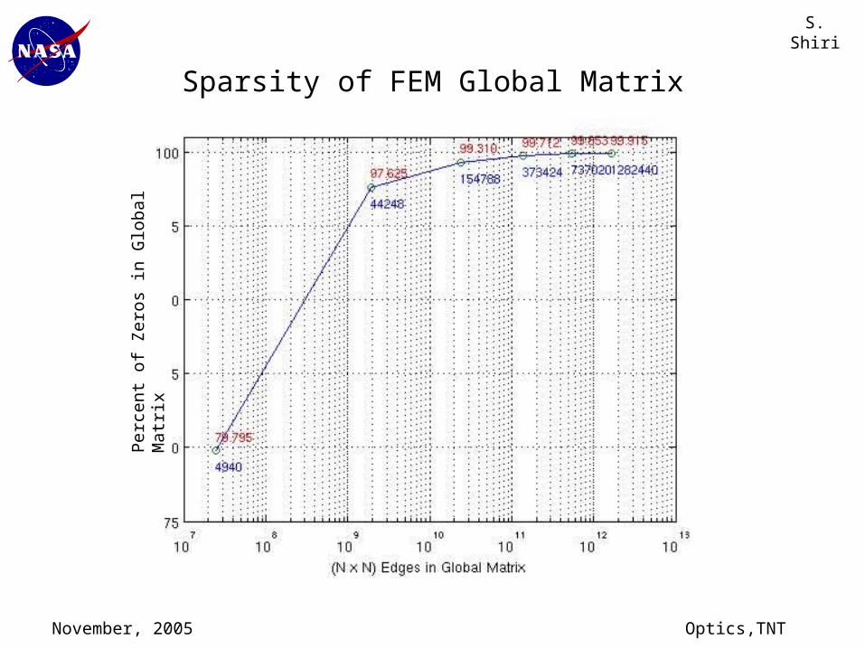
Sparsity of FEM Global Matrix
Per
cen
t of
Zer
os
in G
lob
al M
atrix

November, 2005 Optics,TNT
S. Shiri
Computational Assessment of Helmholtz Solver Using Krylov Subspace

November, 2005 Optics,TNT
S. Shiri
• Transverse Electric Field (TE) Propagating from Front Panel in Rectangular Waveguide is Characterized by, and and only mode of operation is
• In Dominant Mode TE10 , can be derived from
• Subject to Boundary Conditions, • and
• Then, and
•
0zE y
x
z
0zH 0zE ( )yE z
( )yE z
( ) cos sinyE z E kz E kz
00( )y zE z E ( )ey e zE z E
0zE E 0cos
sinez z e
e
E E kzE
kz
0
0
cos( ) cos sin
sinez z e
y ze
E E kzE z E kz kz
kz
0z
ez
a• Where,
22
cka
c j r
Solution Derived from “Foundationsof Optical Waveguides” by G. Owyang
Vector Model Verification Using Analytic Waveguide Propagation in Rectangular Slab

November, 2005 Optics,TNT
S. Shiri
Waveguide Validation: Electric Field Propagation in
Lossless Hollow Rectangular Waveguide
Geometry: Hollow rectangular box 8 x 4 x 48 cmIncident Beam: Y-Polarized incident from left, Wavelength = 15 cmPermittivity = 3.0 and Conductivity = 0.02
Electric Field Propagation in Lossless Material Open-End Permittivity=2.0
-1.5
-1
-0.5
0
0.5
1
1.5
E (real)

November, 2005 Optics,TNT
S. Shiri
Waveguide Validation: Electric Field Propagation in
Lossy Hollow Rectangular Waveguide
Geometry: Hollow rectangular box 8 x 4 x 48 cmIncident Beam: Y-Polarized incident from left, Wavelength = 15 cmPermittivity = 3.0 and Conductivity = 0.02
Electic Field Propagation in Lossy Material Open- End Permittivity=3.0, Conductivity=0.02
-1
-0.8
-0.6
-0.4
-0.2
0
0.2
0.4
0.6
0.8
1
E (Real)
E (Im)
November, 2005 Optics,TNT
S. Shiri
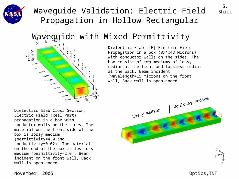
Dielectric Slab: |E| Electric Field Propagation in a box (8x4x48 Microns) with conductor walls on the sides. The box consist of two mediums of lossy medium at the front and lossless medium at the back. Beam incident (wavelength=15 micron) on the front wall, Back wall is open-ended.
Dielectric Slab Cross Section: Electric Field (Real Part) propagation in a box with conductor walls on the sides. The material on the front side of the box is lossy medium (permittivity=4.0 and conductivity=0.02). The material on the end of the box is lossless medium (permittivity=2.0). Beam incident on the front wall, Back wall is open-ended.
Lossy mediumNonlossy medium
Waveguide Validation: Electric Field Propagation in
Hollow Rectangular Waveguide with Mixed Permittivity

November, 2005 Optics,TNT
S. Shiri
Waveguide Validation: Electric Field Propagation in Hollow Rectangular Waveguide with Mixed Permittivity
Geometry: Hollow rectangular box 8 x 4 x 48 cmIncident Beam: Y-Polarized incident from left, Wavelength = 15 cmPermittivity = 3.0 and Conductivity = 0.02
Electric Field Propagation in Two-Layer Lossy (Permittivity=4.0,Conductivity=0.02) and Nonlossy
(Permittivity=2.0) Medium
-1.5
-1
-0.5
0
0.5
1
1.5
( E)R
( E)Im
|E|

November, 2005 Optics,TNT
S. Shiri
Vector FEM Verification: Rectangular Waveguide Case – Lossy Medium
VFEM Verification: Geometry - Hollow rectangular waveguide 8 x 4 x 32 cm, Incident Beam – Planar 15 cm wavelength. Boundaries - Perfect conductor at the walls. Filling Medium – Non magnetic dielectric with permittivity = 3.0 + 0.04i
Z-axis (m)

November, 2005 Optics,TNT
S. Shiri
Vector FEM Verification: Rectangular Waveguide Case – Lossless Medium
VOM Verification: Geometry - Hollow rectangular waveguide 8 x 4 x 32 cm, Incident Beam – Planar 15 cm wavelength. Boundaries - Perfect conductor at the walls. Filling Medium – Non magnetic dielectric with permittivity = 2.0
Z-axis (m)

November, 2005 Optics,TNT
S. Shiri
Glass
Gold
Vacumm
Plane Wave = 0.6 mm
18 m
101
100
10-2
10-3
10-4
10-5
10-1
= 0.6 m, 6 m of Gold thickon 5 m of glass, 18 x 18 um box
FEM Verification: Electric Field Propagation around Gold Metallic Mask
Profile of Magnitude of Electric Field
Thickness (microns)

November, 2005 Optics,TNT
S. Shiri
Columbia Project Vector Finite Element Simulation
Simulation of vector diffraction model:
Geometry: 20x20x10 microns Filling: AirMask: Silver, 5x5x1 micronsIncident Beam: Planar, y-polarized, wavelength of 5 micronsBoundary: PML absorbing boundaries
X-cross section,Red line: Intensity profile before mask
Y-cross section,Black line: Intensity profile after mask
Z-cross section, Red line: Intensity profile before maskBlack line: Intensity profile after mask
Numerical Complexity:
Edges: 6 millionsNodes: 646400Memory: 350 Gig. BytesCPUs: 100Convergence Time: 7 Hrs.

November, 2005 Optics,TNT
S. Shiri
Columbia Project Vector Finite Element Simulation
After Mask
Before Mask
X- axis Profile X- axis Profile
Electric Field Intensity Log Profile Electric Field Intensity Linear Profile
Columbia Project vector finite element simulation of planar incident beam into geometry air filled centered with circular silver mask. Beam Properties: Planar, Wavelength of 5 microns, y-polarized Geometry: 20 x 20 x 10 microns Boundary: PML absorbing boundaries

November, 2005 Optics,TNT
S. Shiri
Electric Field Before and After Circular Mask
Profile of electric field before and after a circular mask in a vacuum. The mask is silver metallic disk. The incident beam is planar and polarized in y direction with wavelength of 5 microns.

November, 2005 Optics,TNT
S. Shiri
Limitations of Vector FEM
• Computationally expensive to achieve 108 accuracy or higher
• A sample realistic simulation requires
– Large amount of memory (Gigabytes)
– Matrix Solver based on MPI requires cluster to reach convergence in a reasonable time frame
– More than 72 samples per wavelength
• Selecting appropriate Absorbing Boundary Condition (ABC) far away from the object
3102020 xx

November, 2005 Optics,TNT
S. Shiri
Summary
• Formulated a vector model for the electric field around the mask in TPF coronagraph
• Incorporated and configured the Vector Finite Element Method (VFEM) for this problem
• Verified the accuracy of VFEM for TPF using analytical solutions in rectangular waveguide to 10
– VFEM shows promise of being used for further highly accurate models around or near the mask