s32r274, s32r274 data sheet - nxp semiconductors · pdf files32r274 s32r274 data sheet ......
TRANSCRIPT
S32R274S32R274 Data SheetFeatures
• On-chip modules available within the device includethe following features:
• Safety core: Power Architecture® e200Z4 32-bit CPUwith checker core
• Dual issue computation cores: Power Architecture®e200Z7 32-bit CPU
• 2 MB on-chip code flash (FMC flash) with ECC
• 1.5 MB on-chip SRAM with ECC
• RADAR processing– Signal Processing Toolbox (SPT) for RADAR signal
processing acceleration– Cross Timing Engine (CTE) for precise timing
generation and triggering– Waveform generation module (WGM) for chirp
ramp generation– 4x 12-bit ΣΔ-ADC with 10 MSps– One DAC with 10 MSps– MIPICSI2 interface to connect external ADCs
• Memory Protection– Each core memory protection unit provides 24
entries– Data and instruction bus system memory protection
unit (SMPU) with 16 region descriptors each– Register protection
• Clock Generation– 40 MHz external crystal (XOSC)– 16 MHz Internal oscillator (IRCOSC)– Dual system PLL with one frequency modulated
phase-locked loop (FMPLL)– Low-jitter PLL to ΣΔ-ADC and DAC clock
generation
• Functional Safety– Enables up to ASIL-D applications– FCCU for fault collection and fault handling– MEMU for memory error management– Safe eDMA controller– Self-Test Control Unit (STCU2)– Error Injection Module (EIM)– On-chip voltage monitoring– Clock Monitor Unit (CMU)
• Security– Cryptographic Security Engine (CSE2)– Supports censorship and life-cycle management
• Timers– Two Periodic Interval Timers (PIT) with 32-bit
counter resolution– Three System Timer Module (STM)– Three Software Watchdog Timers (SWT)– Two eTimer modules with 6 channels each– One FlexPWM module for 12 PWM signals
• Communication Interfaces– Two Serial Peripheral interface (SPI) modules– One LINFlexD module– Two inter-IC communication interface (I2C)
modules– One dual-channel FlexRay module with 128
message buffers– Three FlexCAN modules with configurable buffers -
CAN FD optionally supported on 2 FlexCANmodules
– One ENET MAC supporting MII/RMII/RGMIIinterface
– ZipWire high-speed serial communication
• Debug Functionality– 4-pin JTAG interface and Nexus/Aurora interface
for serial high-speed tracing– e200Z7 core and e200Z4 core: Nexus development
interface (NDI) per IEEE-ISTO 5001-2012 Class 3+
• Two analog-to-digital converters (SAR ADC)– Each ADC supports up to 16 input channels– Cross Trigger Unit (CTU)
• On-chip voltage DC/DC regulator for core clock(VREG)
• Two Temperature Sensors (TSENS)
NXP Semiconductors Document Number S32R274
Data Sheet: Technical Data Rev. 3.2, 07/2017
NXP reserves the right to change the production detail specifications as may berequired to permit improvements in the design of its products.

S32R274 Data Sheet, Rev. 3.2, 07/2017
2 NXP Semiconductors

Table of Contents1 Introduction........................................................................................ 4
1.1 Family comparison..................................................................4
1.2 Feature list............................................................................... 5
1.3 Block diagram......................................................................... 9
2 Ordering parts.....................................................................................9
2.1 Determining valid orderable parts...........................................9
3 Part identification............................................................................... 10
3.1 Description.............................................................................. 10
3.2 Format..................................................................................... 10
3.3 Fields....................................................................................... 10
4 General............................................................................................... 11
4.1 Introduction............................................................................. 11
4.2 Absolute maximum ratings..................................................... 12
4.3 Operating conditions............................................................... 13
4.4 Supply current characteristics................................................. 15
4.5 Voltage regulator electrical characteristics............................. 16
4.6 Electromagnetic Compatibility (EMC) specifications............ 20
4.7 Electrostatic discharge (ESD) characteristics......................... 20
5 I/O Parameters....................................................................................21
5.1 I/O pad DC electrical characteristics ......................................21
5.2 I/O pad AC specifications....................................................... 22
5.3 Aurora LVDS driver electrical characteristics........................ 23
5.4 Reset pad electrical characteristics..........................................24
6 Peripheral operating requirements and behaviours............................ 26
6.1 Clocks and PLL Specifications............................................... 26
7 Analog modules................................................................................. 29
7.1 ADC electrical characteristics.................................................29
7.2 Sigma Delta ADC electrical characteristics............................ 33
7.3 DAC electrical specifications..................................................37
8 Memory modules............................................................................... 38
8.1 Flash memory program and erase specifications.................... 38
8.2 Flash memory Array Integrity and Margin Read
specifications...........................................................................39
8.3 Flash memory module life specifications................................39
8.4 Data retention vs program/erase cycles...................................40
8.5 Flash memory AC timing specifications.................................40
8.6 Flash memory read wait-state and address-pipeline control
settings.....................................................................................41
9 Communication modules................................................................... 42
9.1 Ethernet switching specifications............................................42
9.2 FlexRay timing parameters..................................................... 46
9.3 LVDS Fast Asynchronous Transmission (LFAST) electrical
characteristics.......................................................................... 50
9.4 Serial Peripheral Interface (SPI) timing specifications........... 54
9.5 LINFlexD timing specifications..............................................59
9.6 I2C timing .............................................................................. 59
10 Debug modules...................................................................................60
10.1 JTAG/CJTAG interface timing .............................................. 60
10.2 Nexus Aurora debug port timing.............................................63
11 WKUP/NMI timing specifications.....................................................64
12 External interrupt timing (IRQ pin)................................................... 65
13 Temperature sensor electrical characteristics.....................................65
14 Radar module..................................................................................... 66
14.1 MIPICSI2 D-PHY electrical and timing specifications.......... 66
14.2 MIPICSI2 Disclaimer..............................................................69
15 Thermal Specifications.......................................................................71
15.1 Thermal characteristics........................................................... 71
16 Packaging........................................................................................... 73
17 Reset sequence................................................................................... 73
17.1 Reset sequence duration.......................................................... 74
17.2 Reset sequence description......................................................74
18 Power sequencing requirements.........................................................76
19 Pinouts................................................................................................77
19.1 Package pinouts and signal descriptions................................. 77
20 Revision History.................................................................................77
S32R274 Data Sheet, Rev. 3.2, 07/2017
NXP Semiconductors 3
Introduction
1.1 Family comparison
The following table provides a comparison of two devices S32R274 and MPC5775K .This information is intended to provide an understanding of the range of functionalityoffered by this family. For full details of all of the family derivatives please contact yourmarketing representative.
Table 1. S32R274 Family Comparison
Feature S32R274 MPC5775K
CPUs e200z420 lock-step
2x e200z7260
SIMD SPE2 + EFP2 (z7)
Maximum Operating Frequency 240 MHz (z7 cores) / 180 MHz (z4) 266 MHz (z7 cores) / 133 MHz (z4)
Flash 2 MB with ECC 4 MB with ECC
EEPROM support 64 KB (emulation) 96 KB (emulation)
RAM 1.5 MB with ECC
ECC end-to-end
MPU Core MPU: 24 entries per core, System MPU: 2x16 entries
eDMA safe eDMA with 32 channels, 64 triggers
Control ADC 2x 12-bit SAR ADC, 1 MSps input muxfor 16 external channels
4x 12-bit SAR ADC, 1 MSps, input muxfor 37 external channels
SD-ADC 4 channels, 10 MSps 8 channels, 10 MSps
SPT 1x
CTE 1x
WGM 1x
CTU 1x 2x
SWT 3x
STM 3x
PIT 2x
CRC 2x
SEMA42 1x
LINFlexD 1x 4x
CAN 3x FlexCAN including 2x FlexCAN-FD 4x FlexCAN + 1x MCAN-FD
SPI 2x 4x
I2C 2x 3x
Zipwire 1x LFAST+SIPI, 320 MHz
FlexRay 1x dual channel
Table continues on the next page...
1
Introduction
S32R274 Data Sheet, Rev. 3.2, 07/2017
4 NXP Semiconductors

Table 1. S32R274 Family Comparison (continued)
Feature S32R274 MPC5775K
Ethernet 10/100 and >100 Mbps, RMII/MII/RGMIII/F, AVB support
10/100 Mbps, RMII/MII I/F, AVB support
FlexPWM 1x, 12 PWM channels 2x, 12 PWM channels each
eTimer 2x, 6 channels each 3x, 6 channels each
External ADC interface 1x 4 lanes MIPICSI2 Rx, 1 Gbps/lane 1x PDI (16-bit data, clock, sync)
IRCOSC 16 MHz
XOSC 40 MHz
FMPLL dual system PLL, 1x FM modulated
DAC 1x 12-bit 10 MSps 1x 12-bit 2 MSps
SIUL2 1x
BAM 1x
INTC 1x
SSCM 1x
FCCU/FOSU 1x
MEMU 1x
STCU2 1x
CSE 1x -
PASS/TDM 1x -
MC_ME 1x
MC_CGM 1x
MC_RGM 1x
TSENS 2x
Debug JTAGC, JTAGM, CJTAG, with class3+ Nexus, Aurora only
Safety level ISO26262 SEooC ASIL-B to ASIL-D
Temp. range (Tj) -40 to 150˚C
1.2 Feature list
On-chip modules available within the device include the following features:
• Safety core: Power Architecture® e200Z4 32-bit CPU with checker core• 2 cycle delayed lockstep• Harvard architecture with 64-bit bus for data and instructions• Dual issue: up to two instructions per clock cycle• 8 KB instruction cache and 4 KB data cache• 64 KB data local memory
• with background load/store: backdoor access• 0-wait state for all read and 32/64-bit write accesses• Low number of wait states for backdoor accesses
Introduction
S32R274 Data Sheet, Rev. 3.2, 07/2017
NXP Semiconductors 5

• Support for decorated storage• Variable Length Encoding (VLE) compliant for higher code density• Single precision floating point operations
• Computation cores: Power Architecture® e200Z7 32-bit CPU• Dual issue: up to two instructions per clock cycle• Harvard architecture with 64-bit bus for data instructions• 16 KB instruction cache and 16 KB data cache• 64 KB data local memory
• with background load/store: backdoor access• 0-wait state for all read and 32/64-bit write accesses• Low number of wait states for backdoor accesses
• Support for decorated storage• Using variable length encoding (VLE) for higher code density• 4-way integer processing unit (SPE2)• 2-way single-precision Floating Point Unit (EFPU2)
• 2 MB on-chip code flash (FMC flash) with ECC• Three ports (one per CPU) shared between code and data flash with 4 × 256 bit
buffer for code and data flash including prefetch functions• Data flash is part of the code flash module• Including 64 KB EEPROM emulation
• 1.5 MB on-chip SRAM with ECC• Decorated memory controller to support atomic read-modify-write operations• Single- and double-bit error visibility is supported• Up to four ports (one per CPU and SPT) and up to 8 banks allow simultaneous
accesses from different masters to different banks• RADAR processing
• Signal Processing Toolbox (SPT) for RADAR signal processing acceleration• Cross Timing Engine (CTE) for precise timing generation and triggering• Waveform generation module (WGM) for chirp ramp generation• 4x 12-bit ΣΔ-ADC with 10 MSps• One DAC with 10 MSps• MIPICSI2 interface to connect external ADCs
• Four data lanes, with up to 1 Gbps per lane and in total• One clock lane
• Memory Protection• Each core memory protection unit provides 24 entries• Data and instruction bus system memory protection Unit (SMPU) with 16 region
descriptors each• Register protection
• Clock Generation• 40 MHz external crystal (XOSC)
Introduction
S32R274 Data Sheet, Rev. 3.2, 07/2017
6 NXP Semiconductors
• 16 MHz Internal oscillator (IRCOSC)• Dual system PLL with one frequency modulated phase-locked loop (FMPLL)• Low-jitter PLL to ΣΔ-ADC and DAC clock generation
• Functional Safety• Enables up to ASIL-D applications• End to end ECC ensuring full protection of all data accesses throughout the
system, from each of the systems masters through the crossbar and into thememories and peripherals
• FCCU for fault collection and fault handling• MEMU for memory error management• Safe eDMA controller• User selectable Memory BIST (MBIST) can be enabled to run out of various
reset conditions or during runtime• Self-Test Control Unit (STCU2)• Error Injection Module (EIM)• On-chip voltage monitoring• Clock Monitor Unit (CMU) to support monitoring of critical clocks
• Security• Cryptographic Security Engine (CSE2) enabling advanced security management• Supports censorship and life-cycle management via Password and Device
Security (PASS) module• Diary control for tamper detection (TDM)
• Support Modules• Global Interrupt controller (INTC) capable of routing interrupts to any CPU• Semaphore unit to manage access to shared resources• Two CRC computation units with four polynomials• 32-channel eDMA controller with multiple transfer request sources using
DMAMUX• Boot Assist Module (BAM) supports internal flash programming via a serial link
(LIN / CAN)• Timers
• Two Periodic Interval Timers (PIT) with 32-bit counter resolution• Three System Timer Module (STM)• Three Software Watchdog Timers (SWT)• Two eTimer modules with 6 channels each• One FlexPWM module for 12 PWM signals
• Communication Interfaces• Two Serial Peripheral interface (SPI) module• Two inter-IC communication interface (I2C) modules• One LINFlexD module• One dual-channel FlexRay module with 128 message buffers
Introduction
S32R274 Data Sheet, Rev. 3.2, 07/2017
NXP Semiconductors 7
• Three FlexCAN modules with configurable buffers• CAN FD optionally supported on 2 FlexCAN modules
• One ENET MAC supporting MII/RMII/RGMII interface• Supports 10/100 Mbps (MII/RMII/RGMII) and >100 Mbps (RGMII)• Supports IEEE1588 timestamps and PTP
• Zipwire high-speed serial communication• Supports LFAST and SIPI protocol• Fast interprocessor communication with 320 Mbps gross data rate• DMA based access to memory resources
• Debug Functionality• 4-pin JTAG interface and Nexus/Aurora interface for serial high-speed tracing• e200Z7 core and e200Z4 core: Nexus development interface (NDI) per IEEE-
ISTO 5001-2012 Class 3+• All platform bus masters except CSE can be monitored via Nexus/Aurora• Device/board boundary Scan testing supported with per Joint Test Action Group
(JTAG) (IEEE 1149.1) and 1149.7 (cJTAG)• On-chip control for Nexus development interface by JTAGM module
• Two analog-to-digital converters (SAR ADC)• Each ADC supports up to 16 input channels• Cross Trigger Unit to enable synchronization of ADC conversions with eTimer
• On-chip voltage DC/DC regulator for core clock (VREG)• Two Temperature Sensors (TSENS)
Introduction
S32R274 Data Sheet, Rev. 3.2, 07/2017
8 NXP Semiconductors

1.3 Block diagram
SignalProcessingToolbox (SPT)
Safety Lake
EN
ET
eD
MA
e2
eE
CC
DM
AM
UX
eD
MA
e2
eE
CC
Delay/RCCU
AcquisitionFFT/
ProcessingSequencer
LocalSRAM(ECC) FastDMA
e2eECC
Data Crossbar Switch (AMBA 2.0 v6 AHB) 64 bit
System memory Protection Unit SMPU_0
4x analog diff. input
4x lanes+ clock
Nexus DataTrace
Nexus DataTrace
e2eECC
E200z420Core0
VLE
Nexus3+
FPU
Core MPU 24 Entries
64 KBDTCM
4 KBDCache
8 KBICache
TC
M B
ackd
oo
r e
2e
EC
C
SWT_0
STM_0
JTAGC
CJTAG
NAL
e200z419Checker Core0
VLE
FPU
Core MPU 24 Entries TC
M B
ackd
oo
r e
2e
EC
C
Delay/RCCU
Delay/RCCU
Instr. Crossbar Switch (AMBA 2.0 v6 AHB) 64- bit
System memory Protection Unit SMPU_1AH
BB
ridge_0
AH
BB
ridge_1
NPC
Triple PortedFlash Controller
(PFLASH)e2eECC
2 MB Flash memory
up to 64 KB DFlash
ECC
Core
_1
Quad PortedSRAM Controller
(PRAM)e2eECC
1.5 MB SRAM8 Banks
ECC
Co
re_
0+
all
oth
ers
SP
T
DMASRAM(ECC)
AIPS-Lite_0e2eECC
AIPS-Lite_1
e2eECC
32-b
it
32-b
itA
IPS
-Lite
_0
AX
BS
_0
AX
BS
_1
SM
PU
_0
SM
PU
_1
PR
AM
PF
LA
SH
SE
MA
42
INT
C
SW
T_
0
SW
T_
1
ST
M_
0
ST
M_
1
eD
MA
EN
ET
eT
ime
r_1
Fle
xP
WM
_0
AD
C_
1
SP
I_1
LIN
Fle
xD
Fle
xC
AN
_0
Fle
xR
AY
PIT
_0
PIT
_1
SS
CM
BA
M
AIP
S-L
ite
_1
SD
AD
C[0
:3]
SD
PL
L
SD
VR
eg
s
XO
SC
DA
C
eT
ime
r_2
CT
U_
0
AD
C_
0
I2C
_1
SP
I_2
BIU e2eECCBIU e2eECC
Fle
xC
AN
_2
TC
M_C
ore
0/1
/2
e200z7260Core1
VLE
Nexus3+
SPE2
VFPU
BIU e2eECCCore MPU 24 Entries
64 KBDTCM16 KB
DCache16 KB
ICache
TC
M B
ackd
oo
r e
2e
EC
C
SWT_1
STM_1
D
Bus
D
Bu
s
IB
us
IB
us
Core
_1
async
FC
CU
CR
C_
1C
RC
_1
CR
C_
1C
MU
s
Core
_2/
CS
E
CT
E_
0
WG
M_
0
NAP
DTS
Cal
Zip
wire
ZipwireMII/RMII/
RGMII FR
4xSDADC
SDPLL
DualFMPLL
SD VREGs
VREG LVD
XOSC TSENS_0/1
DAC
ST
CU
2M
EM
UC
RC
_0
DM
AM
UX
_0
VR
EG
WK
PU
MC
_R
GM
MC
_C
GM
MC
_M
E
SIU
L2
SIP
I
LFA
ST
_0
SP
T
DM
AM
UX
_1
CSE
IRCOSC
JTA
GM
Co
re_2
MIP
ICS
I2
CS
E
PA
SS
TD
M
e200z7260Core2
VLE
Nexus3+
SPE2
VFPU
BIU e2eECCCore MPU 24 Entries
64 KBDTCM16 KB
DCache16 KBICache
TC
M B
ackd
oo
r e
2e
EC
C
SWT_2
STM_2
IB
us
DB
us
INTC
PIT_0PIT_1
Fle
xC
AN
_1
I2C
_2
SW
T_
2
ST
M_
2
Safety Lake
MIPICSI2
TD
MPA
SS
Fle
xR
ay
Logic
/ A
nalo
gs
Debug
Mem
ori
es
Peri
phera
ls a
lready
show
nexp
licitl
y in
the b
lock
dia
gra
m
Co
re_
0+
all
oth
ers
Nexus DataTrace
e2eECCe2eECC
Figure 1. S32R274 block diagram
Ordering parts
2.1 Determining valid orderable parts
Valid orderable part numbers are provided on the web. To determine the orderable partnumbers for this device, go to www.nxp.com and perform a part number search for thedevice number.
2
Ordering parts
S32R274 Data Sheet, Rev. 3.2, 07/2017
NXP Semiconductors 9

Part identification
3.1 Description
Part numbers for the chip have fields that identify the specific part. You can use thevalues of these fields to determine the specific part you have received.
3.2 Format
Part numbers for this device have the following format: S32R274
3.3 Fields
This section lists the possible values for each field in the part number (not allcombinations are valid):
Product Type/Brand – 32-bit Auto MCU
Core - z7 Power Architecture
Product Line - Radar (R)
S32
R
2
7
M
K
B
Package Suffix - 257 MAPBGA
Tape and Reel Indicator - R (Tape and Reel)
K0 Fab and Mask Revision – K (TSMC14), 0 (MASK)
MM
Temperature Suffix - M (-40 0C to 125 0C Ta), V (-40 0C to 105 0C Ta)
Configuration
Performance
Generation 2nd generation
Product Status - P for prototype and F for qualified ordering part numberF/P
Perf (MHz) Z7 Z7 Z4 Z4 K 240 240 120 120
V 200 200 100 1004 Product, number of cores
Conf. 2 MB Flash 1.5 MB RAM CSE
w/ CSE B Yes Yes Yes w/o CSE C Yes Yes no
R
Figure 2. Commercial product code structure
3
Part identification
S32R274 Data Sheet, Rev. 3.2, 07/2017
10 NXP Semiconductors

Table 2. Configuration
257MAPBGA Configuration Performance Temperature
FS32R274KBK2MMM B K M
FS32R274KCK2MMM C K M
FS32R274VBK2MMM B V M
FS32R274VCK2MMM C V M
FS32R274KBK2VMM B K V
FS32R274KCK2VMM C K V
FS32R274VBK2VMM B V V
FS32R274VCK2VMM C V V
Table 3. Configuration
Configuration 2 MB Flash 1.5 MB RAM CSE
B Yes Yes Yes
C Yes Yes No
Table 4. Performance
Perf (MHz) Z7 Z7 Z4 Z4
K 240 240 120 120
V 200 200 100 100
Table 5. Temperature values
Temperature TA
M -40 oC to 125 oC
V -40 oC to 105 oC
General
4.1 Introduction
The electrical specifications are preliminary and are undergoing initial evaluation. Thesespecifications may not be fully tested or guaranteed at this early stage of the product lifecycle. Finalized specifications will be published after complete characterization anddevice qualifications have been completed.
4
General
S32R274 Data Sheet, Rev. 3.2, 07/2017
NXP Semiconductors 11

4.2 Absolute maximum ratings
NOTE
Functional operating conditions appear in the DC electricalcharacteristics. Absolute maximum ratings are stress ratingsonly, and functional operation at the maximum values is notguaranteed.
Stress beyond the listed maximum values may affect devicereliability or cause permanent damage to the device.
Table 6. Absolute maximum ratings
Symbol Parameter Conditions Min Max Unit
VDD_HV_PMU 3.3 V PMU supply voltage — –0.3 4.01, 2 V
VDD_HV_REG3V8 REG3V8 Supply Voltage — –0.3 5.5 V
VDD_HV_IO* 3.3 V Input/Output Supply Voltage, LFAST IOSupply, RGMII IO Supply and PWM IO Supply
— –0.3 3.631, 2 V
VSS_HV_IOx Input/output ground voltage — –0.1 0.1 V
VDD_HV_FLA 3.3 V flash supply voltage — –0.3 3.631, 2 V
VDD_HV_RAW AFE RAW supply voltage — –0.1 4 V
VDD_HV_DAC AFE DAC supply voltage — –0.1 4 V
VDD_LV_IO* Aurora supply voltage — –0.3 1.5 V
VDD 1.25 V core supply voltage3, 4, 5 — –0.3 1.5 V
VSS 1.25 V core supply ground3, 4, 5 — –0.3 0.3 V
VSS_LV_OSC Oscillator amplifier ground — –0.1 0.1 V
VDD_LV_PLL0 System PLL supply voltage — –0.3 1.5 V
VDD_LV_LFASTPLL LFAST PLL supply voltage — –0.3 1.5 V
VDD_HV_ADCREF0/1 ADC_0 and ADC_1 high reference voltage — –0.3 5.5 V
VSS_HV_ADCREF0/1 ADC_0 and ADC_1 ground and low referencevoltage
— –0.1 0.1 V
VDD_HV_ADC 3.3 V ADC supply voltage — –0.3 4.0 1, 2 V
VSS_HV_ADC 3.3 V ADC supply ground — –0.1 0.1 V
TVDD Supply ramp rate6 — 0.00005 0.1 V/μs
VIN_XOSC Voltage on XOSC pins with respect to ground — -0.3 1.47 V
VINA Voltage on SAR ADC analog pin with respect toground (VSS_HV_ADCREFx)
— –0.3 VDD_HV_ADCREFx+ 0.3
V
VINA_SD Voltage on Sigma-Delta ADC analog pin withrespect to ground7
Powered up 8 -0.3 VDD_HV_RAW +0.3
V
Powered down9
-0.3 1.47
VIN Voltage on any digital pin with respect toground (VSS_HV_IOx)
Relative toVDD_HV_IOx
–0.3 VDD_HV_IOx + 0.310
V
Table continues on the next page...
General
S32R274 Data Sheet, Rev. 3.2, 07/2017
12 NXP Semiconductors

Table 6. Absolute maximum ratings (continued)
Symbol Parameter Conditions Min Max Unit
VDD_LV_DPHY MIPICSI2 DPHY voltage supply3, 4, 5 — –0.3 1.5 V
VSS_LV_DPHY MIPICSI2 DPHY supply ground3, 4, 5 — –0.3 0.3 V
IINJPAD Injected input current on any pin duringoverload condition11
— –10 10 mA
IINJSUM Absolute sum of all injected input currentsduring overload condition
— –50 50 mA
TSTG Storage temperature — –55 150 °C
1. 5.3 V for 10 hours cumulative over lifetime of device; 3.3 V +10% for time remaining.2. Voltage overshoots during a high-to-low or low-to-high transition must not exceed 10 seconds per instance.3. 1.45 V to 1.5 V allowed for 60 seconds cumulative time at maximum TJ = 150°C; remaining time as defined in note 5 and
note 6.4. 1.375 V to 1.45 V allowed for 10 hours cumulative time at maximum TJ = 150°C; remaining time as defined in note 6.5. 1.32 V to 1.375 V range allowed periodically for supply with sinusoidal shape and average supply value below 1.275 V at
maximum TJ=150°C.6. TVDD is relevant for all external supplies.7. ADC inputs include an overvoltage detect function that detects any voltage higher than 1.2 V with respect to ground on
either ADC input and open circuit (disconnect) the input in order to prevent damage to the ADC internal circuitry. The ADCinput remains disconnected until the inputs return to the normal operating range.
8. SDADC is powered up and overvoltage protection is ON.9. SDADC is powered up and overvoltage protection is OFF.10. Only when VDD_HV_IOx < 3.63 V.11. No input current injection circuitry on AFE pins.
4.3 Operating conditionsThe following table describes the operating conditions for the device, and for which allspecifications in the datasheet are valid, except where explicitly noted. The deviceoperating conditions must not be exceeded, or the functionality of the device is notguaranteed.
Table 7. Device operating conditions
Symbol Parameter Conditions Min Typ Max1 Unit
VDD_HV_PMU 3.3V PMU Supply Voltage — 3.132 3.3 3.6 V
VDD_HV_REG3V8 REG3V8 Supply Voltage — 3.13 3.8 5.5 V
VDD Core Supply Voltage — 1.192 1.25 1.313 V
VDD_HV_IO* Main GPIO 3V Supply Voltage, LFASTIO Supply, RGMII IO Supply, PWM IOSupply Voltage
— 3.132 3.3 3.6 V
VDD_LV_IO_*4 Aurora Supply Voltage — 1.19 1.25 1.31 V
VDD_LV_PLL0 System PLL Supply Voltage — 1.192 — 1.31 V
VDD_LV_LFASTPLL LFAST PLL Supply Voltage — 1.19 — 1.31 V
VDD_HV_FLA5 Flash Supply Voltage — 3.132 3.3 3.6 V
Table continues on the next page...
General
S32R274 Data Sheet, Rev. 3.2, 07/2017
NXP Semiconductors 13

Table 7. Device operating conditions (continued)
Symbol Parameter Conditions Min Typ Max1 Unit
VDD_HV_ADC SAR ADC Supply Voltage (HVDsupervised)
— 3.132 3.3 3.66 V
VDD_HV_RAW 3.3V AFE RAW Supply Voltage — 3.13 3.3 3.6 V
VDD_HV_DAC 3.3V AFE DAC Supply Voltage — 3.13 3.3 3.6 V
VDD_HV_ADCREF0/1 ADC_0 and ADC_1 high referencevoltage
— 3.13 3.3 3.6 V
VIN Voltage on digital pin with respect toground (VSS_HV_IOx)
— — — VDD_HV_I
Ox + 0.3V
VINSDPP Sigma-Delta ADC Input Voltage (peak-peak)7, 8
Differential — — 1.2 V
VINSR Sigma-Delta ADC Input Slew Rate7 — — — 165 V/μs
RTRIM_TOL External Trim Resistor tolerance ±0.1% 40.16 40.2 40.25 kΩ
RTRIM_TEMPCO External Trim Resistor TemperatureCoefficient
— — — 25 ppm/°C
VINA9 Voltage on SAR ADC analog pin with
respect to ground (VSS_HV_ADCREFx)— — — VDD_HV_A
DCREFx +0.3
V
VDD_LV_DPHY MIPICSI2 DPHY voltage supply10 1.19 1.25 1.31 V
TA, 11 Ambient temperature at full performance
12— –40 — 125 °C
TJ11 Junction temperature — –40 — 150 °C
FXTAL XOSC Crystal Frequency13 — — 40 — MHz
AFE Bypass Modes Only
Single-Ended External Clock
EXTALclk EXTAL external clock frequency 40 MHz
Vinxoscjit EXTAL external clock Cycle to CycleJitter (RMS)
— — — 2.514 ps
Vinxoscclkvil EXTAL external clock input low voltage — 0 — 0.4 V
Vinxoscclkvih EXTAL external clock input high voltage — 1 — 1.2 V
tr/tf Rise/fall time of EXTAL external clockinput
1 ns
tdc Duty Cycle of EXTAL external clockinput
47 50 53 %
Differential LVDS External Clock
LVDSclk LVDS external clock frequency 40 MHz
LVDSVinxoscclk LVDS external clock input voltage 0 1.36 V
LVDSVinxoscclk(p-p) LVDS external clock input voltage (peak-peak)
Voltage driven,
AC coupled
Differential
0.45 0.70 1.12 V
LVDSIinxoscclk LVDS external clock input current Current driven,
DC coupled.
3.0 3.5 4.0 mA
LVDSVinxoscjit LVDS external clock Jitter (RMS) 14 2.5 ps
Table continues on the next page...
General
S32R274 Data Sheet, Rev. 3.2, 07/2017
14 NXP Semiconductors

Table 7. Device operating conditions (continued)
Symbol Parameter Conditions Min Typ Max1 Unit
tr /tf Rise/fall time of LVDS external clockinput
20% - 80% 1.5 ns
tdcLVDS Duty Cycle of LVDS external clock input 47 50 53 %
1. Full functionality cannot be guaranteed when voltages are out of the recommended operating conditions.2. Min voltage takes into account the LVD variation.3. Max voltage takes into account HVD variation.4. Aurora supply must connect to core supply voltage at board level.5. The ground connection for the VDD_HV_FLA is shared with VSS.6. Supply range does not take into account HVD levels. Full range can be achieved after power-up, if HVD is disabled. See
Voltage regulator electrical characteristics section for details.7. Around common mode voltage of 0.7 V. Input voltage cannot exceed 1.4 V prior to AFE start-up completion (VREF and
VREGs on and LVDs cleared).8. SDADC input voltage full scale is 1.2 Vpp9. On channels shared between ADC0 and 1, VDD_HV_ADCREFx is the lower of VDD_HV_ADCREF0/1.10. VDD_LV_DPHY supply should be shorted to core supply voltage VDD on board. Refer to AN5251. Contact your NXP sales
representative for details.11. While determining if the operating temperature specifications are met, either the ambient temperature or junction
temperature specification can be used. It is critical that the junction temperature specification is not exceeded under anycondition.
12. Full performance means Core0 running @ 120 MHz, Core1/2 running @ 240 MHz, SPT running @ 200 MHz, rich set ofperipherals used.
13. Recommended Crystal 40 MHz (ESR≤30 Ω), 8 pF load capacitance.14. The number is 3.5 ps when SD-ADC and/or DAC is not used in the device.
4.4 Supply current characteristics
Current consumption data is given in the following table. These specifications are designtargets and are subject to change per device characterization.
Table 8. Current consumption characteristics
Symbol Parameter Conditions Min Typ Max Unit
IDD_CORE Core current in run mode All cores at max frequency. 1.31 V. Tj = 150°C - - 14801 mA
IDD_HV_FLA Flash operating current Tj = 150°C. VDD_HV_FLA = 3.6 V - 32 403 mA
IDD_LV_AURORA Aurora operating current Tj = 150°C. VDD_LV_AURORA = 1.31 V. 4 TX lanesenabled.
- - 60 mA
IDD_HV_ADC ADC operating current Tj = 150°C. VDD_HV_ADC = 3.6 V. 2 ADCs operatingat 80 MHz.
- 2 5 mA
IDD_HV_ADCREF Reference current perADC4
Reference current pertemp sensor5
Tj = 150°C. VDD_HV_ADCREFx = 3.6 V. ADC operatingat 80 MHz.
-
-
-
-
1.5
0.75
mA
IDD_HV_RAW AFE SD and regulatoroperating current
Tj = 150°C. VDD_HV_RAW = 3.6 V. SD-PLL, AFEregulators and 4 SD enabled.
- 706 75 mA
IDD_HV_DAC AFE DAC operatingcurrent
Tj = 150°C. VDD_HV_DAC = 3.6 V. DAC enabled. - 10 15 mA
Table continues on the next page...
General
S32R274 Data Sheet, Rev. 3.2, 07/2017
NXP Semiconductors 15
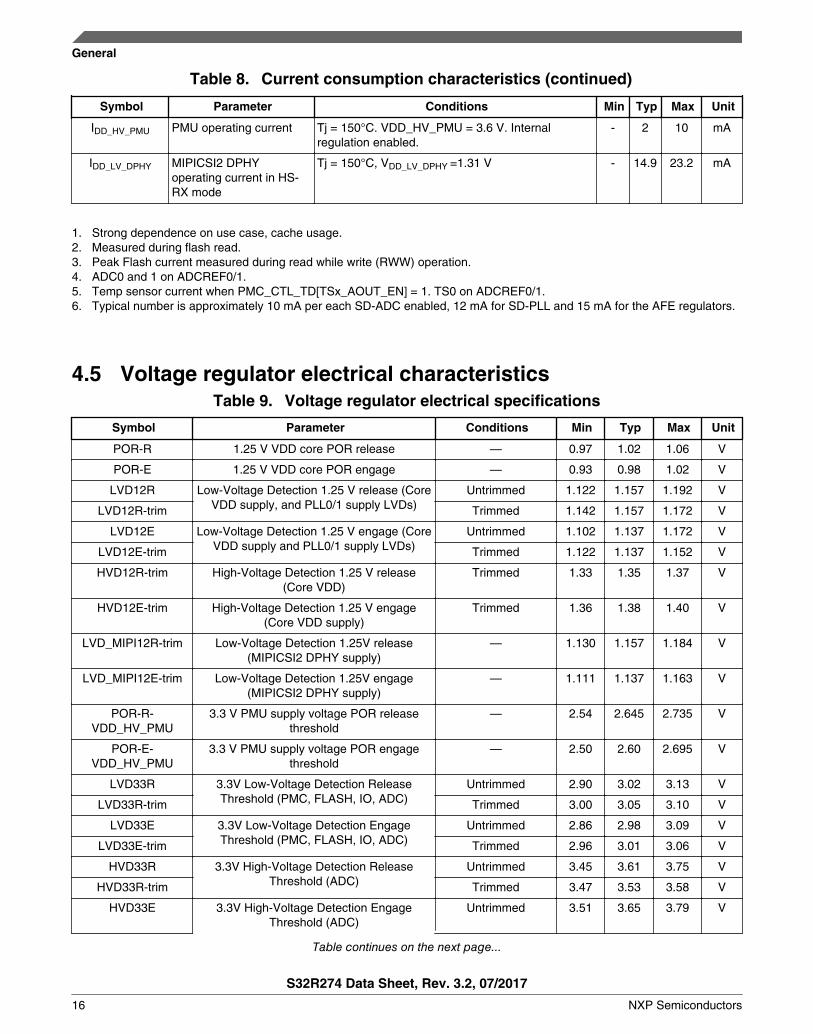
Table 8. Current consumption characteristics (continued)
Symbol Parameter Conditions Min Typ Max Unit
IDD_HV_PMU PMU operating current Tj = 150°C. VDD_HV_PMU = 3.6 V. Internalregulation enabled.
- 2 10 mA
IDD_LV_DPHY MIPICSI2 DPHYoperating current in HS-RX mode
Tj = 150°C, VDD_LV_DPHY =1.31 V - 14.9 23.2 mA
1. Strong dependence on use case, cache usage.2. Measured during flash read.3. Peak Flash current measured during read while write (RWW) operation.4. ADC0 and 1 on ADCREF0/1.5. Temp sensor current when PMC_CTL_TD[TSx_AOUT_EN] = 1. TS0 on ADCREF0/1.6. Typical number is approximately 10 mA per each SD-ADC enabled, 12 mA for SD-PLL and 15 mA for the AFE regulators.
4.5 Voltage regulator electrical characteristicsTable 9. Voltage regulator electrical specifications
Symbol Parameter Conditions Min Typ Max Unit
POR-R 1.25 V VDD core POR release — 0.97 1.02 1.06 V
POR-E 1.25 V VDD core POR engage — 0.93 0.98 1.02 V
LVD12R Low-Voltage Detection 1.25 V release (CoreVDD supply, and PLL0/1 supply LVDs)
Untrimmed 1.122 1.157 1.192 V
LVD12R-trim Trimmed 1.142 1.157 1.172 V
LVD12E Low-Voltage Detection 1.25 V engage (CoreVDD supply and PLL0/1 supply LVDs)
Untrimmed 1.102 1.137 1.172 V
LVD12E-trim Trimmed 1.122 1.137 1.152 V
HVD12R-trim High-Voltage Detection 1.25 V release(Core VDD)
Trimmed 1.33 1.35 1.37 V
HVD12E-trim High-Voltage Detection 1.25 V engage(Core VDD supply)
Trimmed 1.36 1.38 1.40 V
LVD_MIPI12R-trim Low-Voltage Detection 1.25V release(MIPICSI2 DPHY supply)
— 1.130 1.157 1.184 V
LVD_MIPI12E-trim Low-Voltage Detection 1.25V engage(MIPICSI2 DPHY supply)
— 1.111 1.137 1.163 V
POR-R-VDD_HV_PMU
3.3 V PMU supply voltage POR releasethreshold
— 2.54 2.645 2.735 V
POR-E-VDD_HV_PMU
3.3 V PMU supply voltage POR engagethreshold
— 2.50 2.60 2.695 V
LVD33R 3.3V Low-Voltage Detection ReleaseThreshold (PMC, FLASH, IO, ADC)
Untrimmed 2.90 3.02 3.13 V
LVD33R-trim Trimmed 3.00 3.05 3.10 V
LVD33E 3.3V Low-Voltage Detection EngageThreshold (PMC, FLASH, IO, ADC)
Untrimmed 2.86 2.98 3.09 V
LVD33E-trim Trimmed 2.96 3.01 3.06 V
HVD33R 3.3V High-Voltage Detection ReleaseThreshold (ADC)
Untrimmed 3.45 3.61 3.75 V
HVD33R-trim Trimmed 3.47 3.53 3.58 V
HVD33E 3.3V High-Voltage Detection EngageThreshold (ADC)
Untrimmed 3.51 3.65 3.79 V
Table continues on the next page...
General
S32R274 Data Sheet, Rev. 3.2, 07/2017
16 NXP Semiconductors
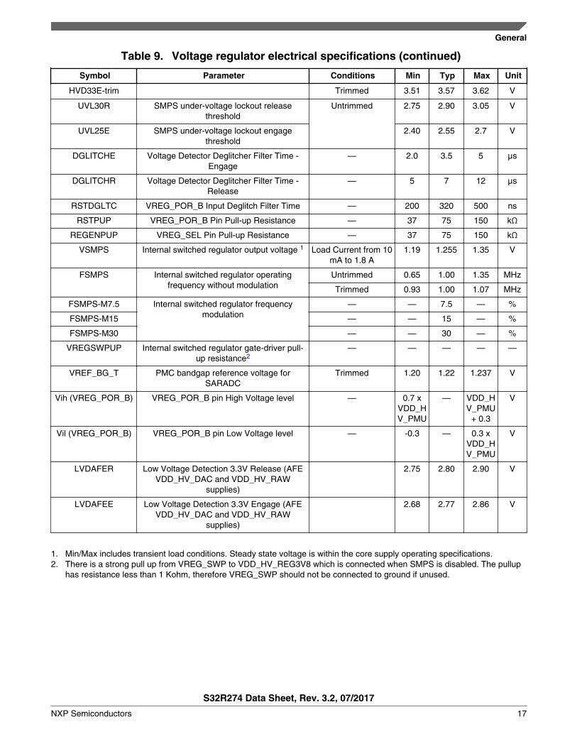
Table 9. Voltage regulator electrical specifications (continued)
Symbol Parameter Conditions Min Typ Max Unit
HVD33E-trim Trimmed 3.51 3.57 3.62 V
UVL30R SMPS under-voltage lockout releasethreshold
Untrimmed 2.75 2.90 3.05 V
UVL25E SMPS under-voltage lockout engagethreshold
2.40 2.55 2.7 V
DGLITCHE Voltage Detector Deglitcher Filter Time -Engage
— 2.0 3.5 5 µs
DGLITCHR Voltage Detector Deglitcher Filter Time -Release
— 5 7 12 µs
RSTDGLTC VREG_POR_B Input Deglitch Filter Time — 200 320 500 ns
RSTPUP VREG_POR_B Pin Pull-up Resistance — 37 75 150 kΩ
REGENPUP VREG_SEL Pin Pull-up Resistance — 37 75 150 kΩ
VSMPS Internal switched regulator output voltage 1 Load Current from 10mA to 1.8 A
1.19 1.255 1.35 V
FSMPS Internal switched regulator operatingfrequency without modulation
Untrimmed 0.65 1.00 1.35 MHz
Trimmed 0.93 1.00 1.07 MHz
FSMPS-M7.5 Internal switched regulator frequencymodulation
— — 7.5 — %
FSMPS-M15 — — 15 — %
FSMPS-M30 — — 30 — %
VREGSWPUP Internal switched regulator gate-driver pull-up resistance2
— — — — —
VREF_BG_T PMC bandgap reference voltage forSARADC
Trimmed 1.20 1.22 1.237 V
Vih (VREG_POR_B) VREG_POR_B pin High Voltage level — 0.7 xVDD_HV_PMU
— VDD_HV_PMU
+ 0.3
V
Vil (VREG_POR_B) VREG_POR_B pin Low Voltage level — -0.3 — 0.3 xVDD_HV_PMU
V
LVDAFER Low Voltage Detection 3.3V Release (AFEVDD_HV_DAC and VDD_HV_RAW
supplies)
2.75 2.80 2.90 V
LVDAFEE Low Voltage Detection 3.3V Engage (AFEVDD_HV_DAC and VDD_HV_RAW
supplies)
2.68 2.77 2.86 V
1. Min/Max includes transient load conditions. Steady state voltage is within the core supply operating specifications.2. There is a strong pull up from VREG_SWP to VDD_HV_REG3V8 which is connected when SMPS is disabled. The pullup
has resistance less than 1 Kohm, therefore VREG_SWP should not be connected to ground if unused.
General
S32R274 Data Sheet, Rev. 3.2, 07/2017
NXP Semiconductors 17
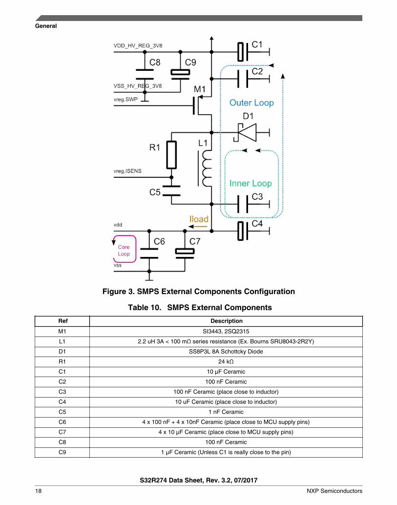
Figure 3. SMPS External Components Configuration
Table 10. SMPS External Components
Ref Description
M1 SI3443, 2SQ2315
L1 2.2 uH 3A < 100 mΩ series resistance (Ex. Bourns SRU8043-2R2Y)
D1 SS8P3L 8A Schottcky Diode
R1 24 kΩ
C1 10 μF Ceramic
C2 100 nF Ceramic
C3 100 nF Ceramic (place close to inductor)
C4 10 uF Ceramic (place close to inductor)
C5 1 nF Ceramic
C6 4 x 100 nF + 4 x 10nF Ceramic (place close to MCU supply pins)
C7 4 x 10 μF Ceramic (place close to MCU supply pins)
C8 100 nF Ceramic
C9 1 μF Ceramic (Unless C1 is really close to the pin)
General
S32R274 Data Sheet, Rev. 3.2, 07/2017
18 NXP Semiconductors
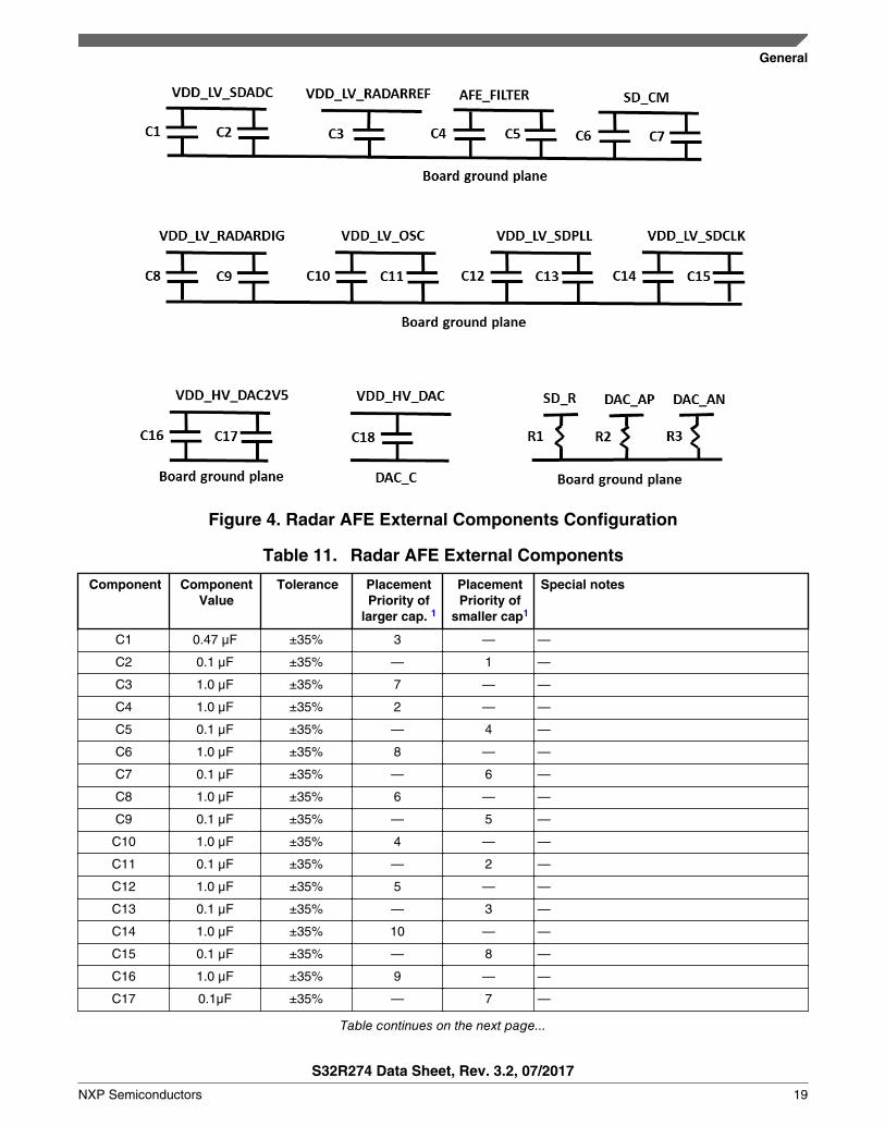
Figure 4. Radar AFE External Components Configuration
Table 11. Radar AFE External Components
Component ComponentValue
Tolerance PlacementPriority of
larger cap. 1
PlacementPriority of
smaller cap1
Special notes
C1 0.47 μF ±35% 3 — —
C2 0.1 μF ±35% — 1 —
C3 1.0 μF ±35% 7 — —
C4 1.0 μF ±35% 2 — —
C5 0.1 μF ±35% — 4 —
C6 1.0 μF ±35% 8 — —
C7 0.1 μF ±35% — 6 —
C8 1.0 μF ±35% 6 — —
C9 0.1 μF ±35% — 5 —
C10 1.0 μF ±35% 4 — —
C11 0.1 μF ±35% — 2 —
C12 1.0 μF ±35% 5 — —
C13 0.1 μF ±35% — 3 —
C14 1.0 μF ±35% 10 — —
C15 0.1 μF ±35% — 8 —
C16 1.0 μF ±35% 9 — —
C17 0.1μF ±35% — 7 —
Table continues on the next page...
General
S32R274 Data Sheet, Rev. 3.2, 07/2017
NXP Semiconductors 19
Table 11. Radar AFE External Components (continued)
Component ComponentValue
Tolerance PlacementPriority of
larger cap. 1
PlacementPriority of
smaller cap1
Special notes
C18 10 μF — 1 — X7R type
C19 220 nF — — — Sigma Delta ADC input capacitor. See Figure10
C20 220 nF — — — Sigma Delta ADC input capacitor. See Figure10
R1 40.2 kΩ ±0.1% — — tempco = 25ppm/C
R2 300 Ω — — — DAC Rl See Table 27
R3 300 Ω — — — DAC Rl See Table 27
Crystal 40MHz — — — Connected between XOSC_EXTAL/XOSC_XTAL, ESR ≤ 30Ω
1. All Radar AFE external bypass capacitors should be placed as close as possible to the associated package pin. As shownin Radar AFE External Components Configuration figure, most pins have two values of bypass capacitor. Greater than 0.1μF is referred to as the larger cap. 0.1 μF is referred to as the smaller cap.
4.6 Electromagnetic Compatibility (EMC) specifications
EMC measurements to IC-level IEC standards are available from NXP on request.
4.7 Electrostatic discharge (ESD) characteristics
Electrostatic discharges (a positive then a negative pulse separated by 1 second) areapplied to the pins of each sample according to each pin combination. The sample sizedepends on the number of supply pins in the device (3 parts × (n + 1) supply pin). Thistest conforms to the AEC-Q100-002/-003/-011 standard.
NOTEA device will be defined as a failure if after exposure to ESDpulses the device no longer meets the device specificationrequirements. Complete DC parametric and functional testingshall be performed per applicable device specification at roomtemperature followed by hot temperature, unless specifiedotherwise in the device specification.
Table 12. ESD ratings
No. Symbol Parameter Conditions1 Class Max value2 Unit
1 VESD(HBM) Electrostatic discharge
(Human Body Model)
TA = 25 °C H1C 2000 V
Table continues on the next page...
General
S32R274 Data Sheet, Rev. 3.2, 07/2017
20 NXP Semiconductors
Table 12. ESD ratings (continued)
No. Symbol Parameter Conditions1 Class Max value2 Unit
conforming to AEC-Q100-002
2 VESD(CDM) Electrostatic discharge
(Charged Device Model)
TA = 25 °C
conforming to AEC-Q100-011
C3A 5003
750 (corners)
V
1. All ESD testing is in conformity with CDF-AEC-Q100 Stress Test Qualification for Automotive Grade Integrated Circuits.2. Data based on characterization results, not tested in production.3. 500 V for non-AFE pins, 250 V for AFE pins.
I/O Parameters
5.1 I/O pad DC electrical characteristicsNMI, TCK, TMS, JCOMP are treated as GPIO.
Table 13. I/O pad DC electrical specifications
Symbol Parameter Value Unit
Min Max
Vih_hys CMOS Input Buffer High Voltage (with hysteresisenabled)
0.65*VDD_HV_IO VDD_HV_IO + 0.3 V
Vil_hys CMOS Input Buffer Low Voltage (with hysteresisenabled)
-0.3 0.35*VDD_HV_IO V
Vih CMOS Input Buffer High Voltage (with hysteresisdisabled)
0.55 * VDD_HV_IO VDD_HV_IO + 0.3 V
Vil CMOS Input Buffer Low Voltage (with hysteresisdisabled)
-0.3 0.40 * VDD_HV_IO V
Vhys CMOS Input Buffer Hysteresis 0.1 * VDD_HV_IO — V
VihTTL TTL Input high level voltage (All SAR_ADC input pins) 2 VDD_HV_ADCREFx+ 0.3
V
VilTTL TTL Input low level voltage (All SAR_ADC input pins) -0.3 0.56 V
VhystTTL TTL Input hysteresis voltage (All SAR_ADC input pins) 0.3 — V
Pull_Ioh Weak Pullup Current1 10 55 µA
Pull_Iol Weak Pulldown Current2 10 55 µA
Iinact_d Digital Pad Input Leakage Current (weak pull inactive) -2.5 2.5 µA
Voh Output High Voltage3 0.8 * VDD_HV_IO — V
Vol Output Low Voltage4 — 0.2 * VDD_HV_IO V
Ioh_f Full drive Ioh5 (ipp_sre[1:0] = 11) 18 70 mA
Iol_f Full drive Iol5 (ipp_sre[1:0] = 11) 21 120 mA
Ioh_h Half drive Ioh5 (ipp_sre[1:0] = 10) 9 35 mA
Iol_h Half drive Iol5 (ipp_sre[1:0] = 10) 10.5 60 mA
5
I/O Parameters
S32R274 Data Sheet, Rev. 3.2, 07/2017
NXP Semiconductors 21

1. Measured when pad = 0 V2. Measured when pad = VDD_HV_IO3. Measured when pad is sourcing 2 mA4. Measured when pad is sinking 2 mA5. Ioh/Iol is derived from spice simulations. These values are NOT guaranteed by test.
5.1.1 RGMII pad DC electrical characteristicsTable 14. RGMII pad DC electrical specifications
Symbol Parameter Value Unit
Min Max
Vih CMOS Input Buffer High Voltage 0.65 x VDD_HV_IO VDD_HV_IO + 0.3 V
Vil CMOS Input Buffer Low Voltage -0.3 0.35 x VDD_HV_IO V
Pull_Ioh Weak Pullup Current1 10 55 µA
Pull_Iol Weak Pulldown Current2 10 55 µA
Iinact_d Digital Pad Input Leakage Current (weak pullinactive)
-2.5 2.5 µA
Voh Output High Voltage3 0.8 x VDD_HV_IO — V
Vol Output Low Voltage4 — 0.2 * VDD_HV_IO V
Ioh_f Full drive Ioh5 8 26 mA
Iol_f Full drive Iol6 8 24 mA
1. Measured when pad = 0 V2. Measured when pad = VDD_HV_IO3. Measured when pad is sourcing 2 mA4. Measured when pad is sinking 2 mA5. Ioh_f value is measured with 0.8*VDDE applied to the pad.6. Iol_f is measured when 0.2*VDDE is applied to the pad.
5.2 I/O pad AC specificationsAC Parameters are specified over the full operating junction temperature range of -40°Cto +150°C and for the full operating range of the VDD_HV_IO supply defined in Table 7.
Table 15. Functional Pad electrical characteristics
Symbol Prop. Delay (ns)1
L>H/H>L
Rise/Fall Edge (ns)2 Drive Load (pF) SIUL2_MSCR[SRC]
Min Max Min Max MSB,LSB
pad_sr_hv
(output)
2.5/2.5 8.25/7.5 0.7/0.6 3/3 50 11
6.4/5 19.5/19.5 2.5/2.0 12/12 200
2.2/2.5 8/8 0.4/0.3 3.5/3.5 25 10
2.9/3.5 12.5/11 1.0/0.8 6.5/6.5 50
11/8 35/31 6.5/3.0 25/21 200
Table continues on the next page...
I/O Parameters
S32R274 Data Sheet, Rev. 3.2, 07/2017
22 NXP Semiconductors

Table 15. Functional Pad electrical characteristics (continued)
Symbol Prop. Delay (ns)1
L>H/H>L
Rise/Fall Edge (ns)2 Drive Load (pF) SIUL2_MSCR[SRC]
Min Max Min Max MSB,LSB
8.3/9.6 45/45 4/3.5 25/25 50 013
13.5/15 65/65 6.3/6.2 30/30 200
13/13 75/75 6.8/6 40/40 50 003
21/22 100/100 11/11 51/51 200
pad_sr_hv
(input)4
2/2 0.5/0.5 0.5 NA
1. As measured from 50% of core side input to Voh/Vol of the output2. Measured from 20% - 80% of output voltage swing3. Slew rate control modes4. Input slope = 2ns
NOTEData based on characterization results, not tested in production.
Table 16. Functional Pad AC Specifications
Symbol Parameter Value Unit
Min Typ Max
pad_sr_hv(Cp) Parasitic Input Pin Capacitance 4.5 4.7 5.0 pF
5.3 Aurora LVDS driver electrical characteristics
NOTEThe Aurora interface is AC coupled, so there is no common-mode voltage specification.
Table 17. Aurora LVDS driver electrical characteristics
Symbol Parameter1 Value Unit
Min Typ Max
FTXRX Data rate — — 1.15 Gbps
Transmitter Specifications
Vdiffout Differential output voltage swing (terminated) +/- 400 +/- 600 +/- 800 mV
Trise/Tfall Rise/Fall time (10% - 90% of swing) 60 ps
Receiver Specifications
Vdiffin Differential voltage +/- 100 +/- 800 mV
Termination
Table continues on the next page...
I/O Parameters
S32R274 Data Sheet, Rev. 3.2, 07/2017
NXP Semiconductors 23

Table 17. Aurora LVDS driver electrical characteristics (continued)
Symbol Parameter1 Value Unit
Min Typ Max
RV_L Terminating Resistance (external) 99 100 101 Ohms
CP Parasitic Capacitance (pad + bondwire + pin) 1 pF
LP Parasitic Inductance 7 nH
STARTUP
TSTRT_BIAS Bias startup time — — 5 µs
TSTRT_TX Transmitter startup time2 — — 5 µs
TSTRT_RX Receiver startup time2 — — 5 µs
LVDS_RXOUT3 Receiver o/p duty cycle 30 70 %
1. Conditions for these values are VDD_LV_IO_AURORA = 1.19V to 1.32V, TJ = –40 / 150 °C2. Startup time is defined as the time taken by LVDS current reference block for settling bias current after its pwr_down
(power down) has been deasserted. LVDS functionality is guaranteed only after the startup time.3. Receiver o/p duty cycle is measured with 1.25 Gbps, 50% duty cycle, max 1 ns rise/fall time, 100 mV voltage swing signal
applied at the receiver input.
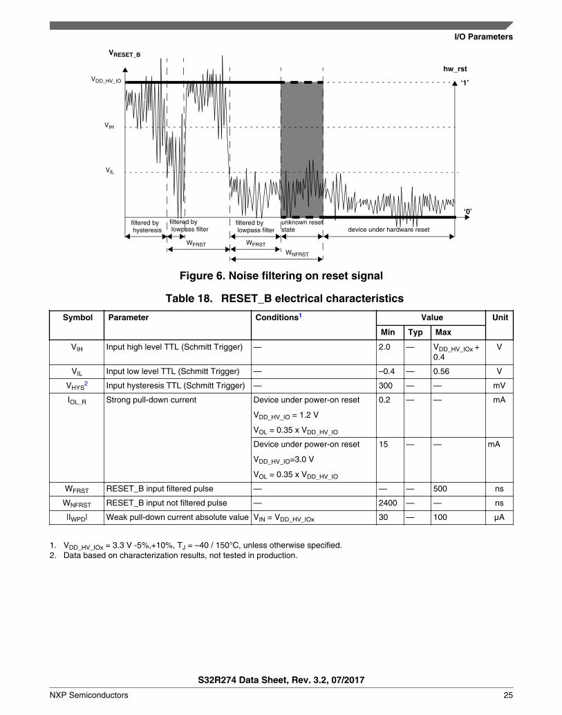
5.4 Reset pad electrical characteristics
The device implements a dedicated bidirectional RESET_B pin.
VIL
VDD_HV_IOx
device reset forced by RESET_B
VDDMIN
RESET_B
VIH
device start-up phase
Figure 5. Start-up reset requirements
I/O Parameters
S32R274 Data Sheet, Rev. 3.2, 07/2017
24 NXP Semiconductors
VRESET_B
VIL
VIH
VDD_HV_IO
filtered by hysteresis
filtered by lowpass filter
WFRST
WNFRST
hw_rst
‘1’
‘0’filtered by lowpass filter
WFRST
unknown resetstate device under hardware reset
Figure 6. Noise filtering on reset signal
Table 18. RESET_B electrical characteristics
Symbol Parameter Conditions1 Value Unit
Min Typ Max
VIH Input high level TTL (Schmitt Trigger) — 2.0 — VDD_HV_IOx +0.4
V
VIL Input low level TTL (Schmitt Trigger) — –0.4 — 0.56 V
VHYS2 Input hysteresis TTL (Schmitt Trigger) — 300 — — mV
IOL_R Strong pull-down current Device under power-on reset
VDD_HV_IO = 1.2 V
VOL = 0.35 x VDD_HV_IO
0.2 — — mA
Device under power-on reset
VDD_HV_IO=3.0 V
VOL = 0.35 x VDD_HV_IO
15 — — mA
WFRST RESET_B input filtered pulse — — — 500 ns
WNFRST RESET_B input not filtered pulse — 2400 — — ns
|IWPD| Weak pull-down current absolute value VIN = VDD_HV_IOx 30 — 100 µA
1. VDD_HV_IOx = 3.3 V -5%,+10%, TJ = –40 / 150°C, unless otherwise specified.2. Data based on characterization results, not tested in production.
I/O Parameters
S32R274 Data Sheet, Rev. 3.2, 07/2017
NXP Semiconductors 25

Peripheral operating requirements and behaviours
Clocks and PLL Specifications
6.1.1 40 MHz Oscillator (XOSC) electrical characteristics
The device provides an oscillator/resonator driver.
NOTEXTAL/EXTAL must not be directly used to drive externalcircuits.
Table 19. XOSC electrical characteristics
Symbol Parameter Conditions Min Typ Max Unit
XOSCfout Oscillator frequency 40 MHz
tstab Oscillator start-up time 2 ms
tjitcc Cycle to cycle jitter (peak –peak)
2.51 ps
Output Duty Cycle 45 50 55 %
Cin Input Capacitance 2 Extal and Xtal each 3.0 4.0 5.0 pF
RinLVDS LVDS bypass mode inputtermination3
Between Extal and Xtal 75 100 125 ohm
VCMLVDS LVDS Common ModeVoltage
Vdda/2 0.60 0.70 0.80 V
1. The number is 3.5 ps when SD-ADC and/or DAC is not used in the device.2. When using a 40 MHz crystal, the recommended load capacitance is 8 pF. Need quiet ground connection on the board
and external crystal/load capacitor placement as close to the Extal and Xtal pins as possible to allow good jitterperformance.
3. The termination resistance is only active when the AFE is powered (VDD_HV_RAW, VDD_HV_DAC and the AFEregulators are powered up) and the XOSC is powered down (default case once device is out of reset) or the XOSC isconfigured in differential bypass mode.
6.1.2 FMPLL electrical characteristics
6
6.1
Peripheral operating requirements and behaviours
S32R274 Data Sheet, Rev. 3.2, 07/2017
26 NXP Semiconductors
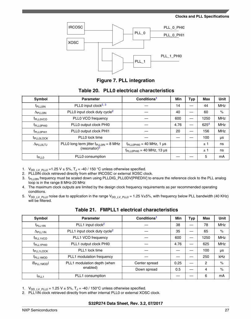
IRCOSC
XOSC PLL_0
PLL_1
PLL_0_PHI0 PLL_0_PHI1
PLL_1_PHI0
Figure 7. PLL integration
Table 20. PLL0 electrical characteristics
Symbol Parameter Conditions1 Min Typ Max Unit
fPLL0IN PLL0 input clock2, 3 — 14 — 44 MHz
PLL0IN PLL0 input clock duty cycle2 — 40 — 60 %
fPLL0VCO PLL0 VCO frequency — 600 — 1250 MHz
fPLL0PHI0 PLL0 output clock PHI0 — 4.76 — 6254 MHz
fPLL0PHI1 PLL0 output clock PHI1 — 20 — 156 MHz
tPLL0LOCK PLL0 lock time — — — 100 µs
PLL0LTJ PLL0 long term jitter fPLL0IN = 8 MHz(resonator)5
fPLL0PHI0 = 40 MHz, 1 μs ± 1 ns
fPLL0PHI0 = 40 MHz, 13 μs ± 1 ns
IPLL0 PLL0 consumption — — 5 mA
1. VDD_LV_PLL0 =1.25 V ± 5%, TJ = -40 / 150 °C unless otherwise specified.2. PLL0IN clock retrieved directly from either IRCOSC or external XOSC clock.3. fPLL0IN frequency must be scaled down using PLLDIG_PLL0DV[PREDIV] to ensure the reference clock to the PLL analog
loop is in the range 8 MHz-20 MHz4. The maximum clock outputs are limited by the design clock frequency requirements as per recommended operating
conditions.5. VDD_LV_PLL0 noise due to application in the range VDD_LV_PLL0 = 1.25 V±5%, with frequency below PLL bandwidth (40 KHz)
will be filtered.
Table 21. FMPLL1 electrical characteristics
Symbol Parameter Conditions1 Min Typ Max Unit
fPLL1IN PLL1 input clock2 — 38 — 78 MHz
PLL1IN PLL1 input clock duty cycle2 — 35 — 65 %
fPLL1VCO PLL1 VCO frequency — 600 — 1250 MHz
fPLL1PHI0 PLL1 output clock PHI0 — 4.76 — 625 MHz
tPLL1LOCK PLL1 lock time — — — 100 µs
fPLL1MOD PLL1 modulation frequency — — — 250 kHz
|δPLL1MOD| PLL1 modulation depth (whenenabled)
Center spread 0.25 — 2 %
Down spread 0.5 — 4 %
IPLL1 PLL1 consumption — — 6 mA
1. VDD_LV_PLL0 = 1.25 V ± 5%, TJ = -40 / 150°C unless otherwise specified.2. PLL1IN clock retrieved directly from either internal PLL0 or external XOSC clock.
Clocks and PLL Specifications
S32R274 Data Sheet, Rev. 3.2, 07/2017
NXP Semiconductors 27

6.1.3 16 MHz Internal RC Oscillator (IRCOSC) electrical specificationsTable 22. Internal RC Oscillator electrical specifications
Symbol Parameter Conditions Min Typ Max Unit
FTarget IRC target frequency — — 16 — MHz
Funtrimmed IRC frequency (untrimmed) — 9.6 — 24 MHz
δFvar IRC trimmed frequency variation 1 — -8 — 8 %
Tstartup Startup time — — 5 µs
1. The typical user trim step size (δfTRIM) is 0.3% of current frequency for application of positive trim and 0.26% of currentfrequency for application of negative trim, based on characterization results.
6.1.4 320 MHz AFE PLL electrical characteristicsTable 23. 320 MHz AFE PLL parameters
Symbol Parameter Conditions Min Typ Max Unit
PLLfout Output Frequency — — 320 — MHz
PLLfin Input Frequency — — — 40 MHz
tcal Calibration Time 1 LW64 = 1
LW64 = 0
— — 150
500
µs
tlock Lock Time after calibration — — 75 µs
tjitcck Cycle to cycle jitter (peak – peak) — — — 10 ps
— Output duty cycle — 48 50 52 %
1. The LW64 bit sets the wait time before the PLL frequency is measured after each calibration step to allow for stabilization.If LW64 is '0', wait time of 256 reference clock cycles is used. If LW64 is'1', wait time of 64 reference clock cycles is used.
6.1.5 LFAST PLL electrical characteristicsThe specifications in the following table apply to the interprocessor bus LFAST interface.
Table 24. LFAST PLL electrical characteristics
Symbol Parameter Condition Min Typ Max Unit
fRF_REF PLL reference clock frequency — 10 — 26 MHz
ERRREF PLL reference clock frequency error — –1 — 1 %
DCREF PLL reference clock duty cycle — 45 — 55 %
fVCO PLL VCO frequency — — 6401 — MHz
tLOCK PLL phase lock2 — — — 40 μs
ΔPERREF Input reference clock jitter (peak to peak) Single period, fRF_REF =10 MHz
— — 300 ps
Table continues on the next page...
Clocks and PLL Specifications
S32R274 Data Sheet, Rev. 3.2, 07/2017
28 NXP Semiconductors

Table 24. LFAST PLL electrical characteristics(continued)
Symbol Parameter Condition Min Typ Max Unit
Long term, fRF_REF = 10MHz
–500 — 500
ΔPEREYE Output Eye Jitter (peak to peak)3 Random Jitter (Rj) — 84 101 ps
Deterministic Jitter (Dj) — 80 96 ps
Total Jitter @BER 10-9 — 1.09 1.31 bitsper
second
IVDD_LV_LFASTPLL VDD_LV_LFASTPLL Supply Current Normal Mode — 6 10 mA
Peak — 7 11 mA
Power Down — 0.5 27 μA
1. The 640 MHz frequency is achieved with a 10 MHz or 20 MHz reference clock. With a 26 MHz reference, the VCOfrequency is 624 MHz.
2. The time from the PLL enable bit register write to the start of phase locks is maximum 2 clock cycles of the peripheralbridge clock that is connected to the PLL on the device.
3. Measured at the transmitter output across a 100 Ω termination resistor on a device evaluation board.
Analog modules
7.1 ADC electrical characteristics
The device provides a 12-bit Successive Approximation Register (SAR) Analog-to-Digital Converter.
7
Analog modules
S32R274 Data Sheet, Rev. 3.2, 07/2017
NXP Semiconductors 29

(2 )
(1)
(3 ) (4)
(5)
Offset Error OSE
Offset Error OSE
Gain Error GE
1 LSB (ideal)
Vin(A) (LSBideal)
(1) Example of an actual transfer curve (2) The ideal transfer curve (3) Differential non-linearity error (DNL) (4) Integral non-linearity error (INL) (5) Center of a step of the actual transfer curve
code out
4095 4094 4093 4092 4091 4090
5 4 3 2 1
0
7 6
1 2 3 4 5 6 7 4089 4090 4091 4092 4093 4094 4095
1 LSB ideal =(VrefH-VrefL)/ 4096 = 3.3V/ 4096 = 0.806 mV Total Unadjusted Error TUE = +/- 6 LSB = +/- 4.84mV
Figure 8. ADC characteristics and error definitions
Analog modules
S32R274 Data Sheet, Rev. 3.2, 07/2017
30 NXP Semiconductors
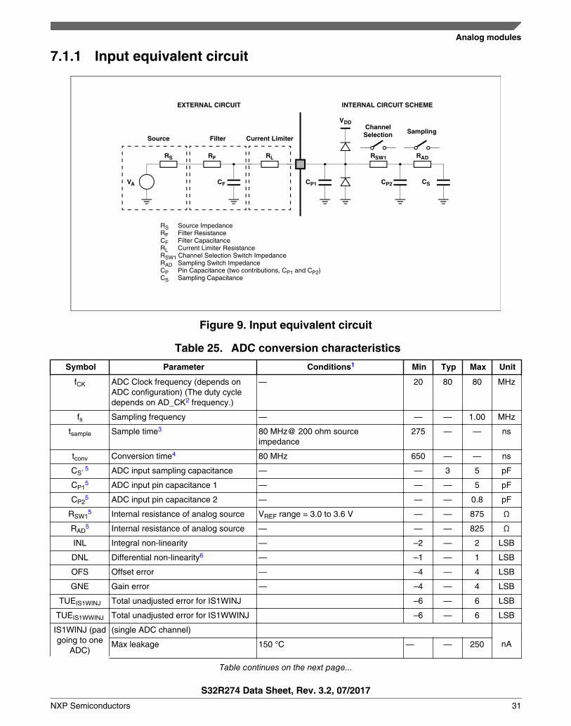
7.1.1 Input equivalent circuit
RF
CF
RS RL RSW1
CP2
VDD
Sampling Source Filter Current Limiter
EXTERNAL CIRCUIT INTERNAL CIRCUIT SCHEME
RS Source Impedance RF Filter Resistance CF Filter Capacitance RL Current Limiter Resistance RSW1 Channel Selection Switch Impedance RAD Sampling Switch Impedance CP Pin Capacitance (two contributions, CP1 and CP2) CS Sampling Capacitance
CP1
RAD
Channel Selection
VA CS
Figure 9. Input equivalent circuit
Table 25. ADC conversion characteristics
Symbol Parameter Conditions1 Min Typ Max Unit
fCK ADC Clock frequency (depends onADC configuration) (The duty cycledepends on AD_CK2 frequency.)
— 20 80 80 MHz
fs Sampling frequency — — — 1.00 MHz
tsample Sample time3 80 MHz@ 200 ohm sourceimpedance
275 — — ns
tconv Conversion time4 80 MHz 650 — — ns
CS, 5 ADC input sampling capacitance — — 3 5 pF
CP15 ADC input pin capacitance 1 — — — 5 pF
CP25 ADC input pin capacitance 2 — — — 0.8 pF
RSW15 Internal resistance of analog source VREF range = 3.0 to 3.6 V — — 875 Ω
RAD5 Internal resistance of analog source — — — 825 Ω
INL Integral non-linearity — –2 — 2 LSB
DNL Differential non-linearity6 — –1 — 1 LSB
OFS Offset error — –4 — 4 LSB
GNE Gain error — –4 — 4 LSB
TUEIS1WINJ Total unadjusted error for IS1WINJ –6 — 6 LSB
TUEIS1WWINJ Total unadjusted error for IS1WWINJ –6 — 6 LSB
IS1WINJ (padgoing to one
ADC)
(single ADC channel)
Max leakage 150 °C — — 250 nA
Table continues on the next page...
Analog modules
S32R274 Data Sheet, Rev. 3.2, 07/2017
NXP Semiconductors 31

Table 25. ADC conversion characteristics (continued)
Symbol Parameter Conditions1 Min Typ Max Unit
Max positive/negative injection –3 — 38 mA
IS1WWINJ(pad going totwo ADCs)
(double ADC channel)
Max leakage 150 °C — — 300 nA
Max positive/negative injection 7 |Vref_ad0 - Vref_ad1| < 150 mV –3.6 — 3.6 mA
SNR Signal-to-noise ratio 3.3 V reference voltage 67 — — dB
THD Total harmonic distortion @ 50 KHz 65 — — dB
SINAD Signal-to-noise and distortion Fin < 50 KHz 6.02 x ENOB + 1.76 dB
ENOB Effective number of bits Fin < 50 KHz 10.5 — — bits
1. VDD_HV_ADC = 3.3 V -5%,+10%, TJ = –40 to +150°C, unless otherwise specified and analog input voltage from VAGND toVDD_HV_ADCREFx.
2. AD_CK clock is always half of the ADC module input clock defined via the auxiliary clock divider for the ADC.3. During the sample time the input capacitance CS can be charged/discharged by the external source. The internal
resistance of the analog source must allow the capacitance to reach its final voltage level within tsample. After the end of thesample time tsample, changes of the analog input voltage have no effect on the conversion result. Values for the sampleclock tsample depend on programming.
4. This parameter does not include the sample time tsample, but only the time for determining the digital result and the time toload the result register with the conversion result.
5. SeeInput equivalent circuit figure.6. No missing codes.7. ADC specifications are met only if injection is within these specified limits8. Max injection current for all ADC IOs is ± 10 mA
NOTEThe ADC performance specifications are not guaranteed if twoADCs simultaneously sample the same shared channel. Aurorainterface along with SAR-ADC would degrade SAR-ADCperformance. General Purpose Input (GPI) functionality shouldnot be used on any of the SAR-ADC channels when SARADCis functional.
Analog modules
S32R274 Data Sheet, Rev. 3.2, 07/2017
32 NXP Semiconductors

7.2 Sigma Delta ADC electrical characteristics
Figure 10. ADC input equivalent circuit
Table 26. Sigma Delta ADC Parameters
Symbol Parameter Condition Min Typ Max Unit
SPSSDA Sample Rate After Decimation Filtering — 10 10 MS/S
LSDA Latency @ 10 MS/s, full step input to 50% output.Decimation filter delay not included
— — 0.1 µs
RTSDA Recovery Time After overload condition — — 0.5 µs
SNRSDA_MM_ON, 1 Signal-to-Noise Ratio
Mismatch Shaper onInput Frequency Range and integrationbandwidth are from 20 KHz to 5 MHz (usingfull-bandwidth decimation filter coefficients).Production test frequencies 449 KHz and 4MHz. Production test amplitude is -6 dBFS =0.6 Vpp.
63 67 — dBFS
Table continues on the next page...
Analog modules
S32R274 Data Sheet, Rev. 3.2, 07/2017
NXP Semiconductors 33
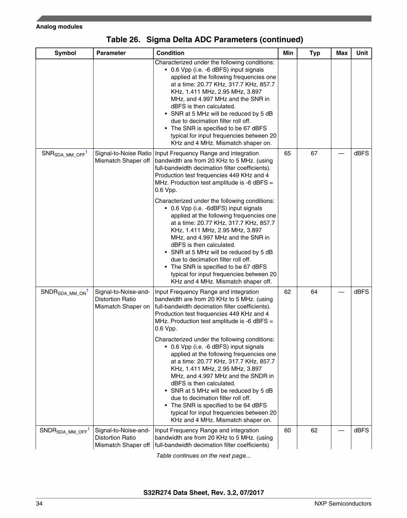
Table 26. Sigma Delta ADC Parameters (continued)
Symbol Parameter Condition Min Typ Max Unit
Characterized under the following conditions:• 0.6 Vpp (i.e. -6 dBFS) input signals
applied at the following frequencies oneat a time: 20.77 KHz, 317.7 KHz, 857.7KHz, 1.411 MHz, 2.95 MHz, 3.897MHz, and 4.997 MHz and the SNR indBFS is then calculated.
• SNR at 5 MHz will be reduced by 5 dBdue to decimation filter roll off.
• The SNR is specified to be 67 dBFStypical for input frequencies between 20KHz and 4 MHz. Mismatch shaper on.
SNRSDA_MM_OFF1 Signal-to-Noise Ratio
Mismatch Shaper offInput Frequency Range and integrationbandwidth are from 20 KHz to 5 MHz. (usingfull-bandwidth decimation filter coefficients).Production test frequencies 449 KHz and 4MHz. Production test amplitude is -6 dBFS =0.6 Vpp.
Characterized under the following conditions:• 0.6 Vpp (i.e. -6dBFS) input signals
applied at the following frequencies oneat a time: 20.77 KHz, 317.7 KHz, 857.7KHz, 1.411 MHz, 2.95 MHz, 3.897MHz, and 4.997 MHz and the SNR indBFS is then calculated.
• SNR at 5 MHz will be reduced by 5 dBdue to decimation filter roll off.
• The SNR is specified to be 67 dBFStypical for input frequencies between 20KHz and 4 MHz. Mismatch shaper off.
65 67 — dBFS
SNDRSDA_MM_ON1 Signal-to-Noise-and-
Distortion RatioMismatch Shaper on
Input Frequency Range and integrationbandwidth are from 20 KHz to 5 MHz. (usingfull-bandwidth decimation filter coefficients).Production test frequencies 449 KHz and 4MHz. Production test amplitude is -6 dBFS =0.6 Vpp.
Characterized under the following conditions:• 0.6 Vpp (i.e. -6 dBFS) input signals
applied at the following frequencies oneat a time: 20.77 KHz, 317.7 KHz, 857.7KHz, 1.411 MHz, 2.95 MHz, 3.897MHz, and 4.997 MHz and the SNDR indBFS is then calculated.
• SNR at 5 MHz will be reduced by 5 dBdue to decimation filter roll off.
• The SNR is specified to be 64 dBFStypical for input frequencies between 20KHz and 4 MHz. Mismatch shaper on.
62 64 — dBFS
SNDRSDA_MM_OFF1 Signal-to-Noise-and-
Distortion RatioMismatch Shaper off
Input Frequency Range and integrationbandwidth are from 20 KHz to 5 MHz. (usingfull-bandwidth decimation filter coefficients)
60 62 — dBFS
Table continues on the next page...
Analog modules
S32R274 Data Sheet, Rev. 3.2, 07/2017
34 NXP Semiconductors

Table 26. Sigma Delta ADC Parameters (continued)
Symbol Parameter Condition Min Typ Max Unit
Production test frequencies 449 KHz and 4MHz. Production test amplitude is -6 dBFS =0.6Vpp.Characterized under the following conditions:
• 0.6 Vpp (i.e. -6 dBFS) input signalsapplied at the following frequenciesapplied one at a time: 20.77 KHz, 317.7KHz, 857.7 KHz, 1.411 MHz, 2.95 MHz,3.897 MHz, and 4.997 MHz and theSNDR in dBFS is then calculated.
• SNR at 5 MHz will be reduced by 5 dBdue to decimation filter roll off.
• The SNR is specified to be 62 dBFStypical for input frequencies between 20KHz and 4 MHz. Mismatch shaper off.
IFDRSDA Interference FreeDynamic Range
20 ms integration, ADC inputs tied together atthe package pin. One side of the AC couplingcapacitors associated with each input shouldremain connected to the ADC input and theother side of the capacitor should connectedto ground.
90 — — dBFS
IMDSDA_MM_ON IntermodulationDistortion MismatchShaper on
Input Frequency Range and integrationbandwidth are from 20 KHz to 5 MHz (usingfull-bandwidth decimation filter coefficients).
Characterized under the following conditions:• Two distinct sets of signal pairs at the
specified frequencies and at anamplitude of -8 dBFs (i.e. 0.23886Vpeak = 0.47772 Vpp differential) areapplied one signal pair at a time.
• Signal pair #1 is f1 = 1 MHz and f2 =1.1 MHz and signal pair #2 is f1 =390.625 KHz and f2 = 546.875 KHz.
• All inter modulation products arechecked. Mismatch Shaper on.
62 — — dBc
IMDSDA_MM_OFF IntermodulationDistortion MismatchShaper off
Input Frequency Range and integrationbandwidth are from 20 KHz to 5 MHz (usingfull-bandwidth decimation filter coefficients).
Characterized under the following conditions:• Two distinct sets of signal pairs at the
specified frequencies and at anamplitude of -8 dBFs (i.e. 0.23886Vpeak = 0.47772 Vpp differential) areapplied one signal pair at a time.
• Signal pair #1 is f1 = 1 MHz and f2 =1.1 MHz and signal pair #2 is f1 =390.625 KHz and f2 = 546.875 KHz.
• All inter modulation products arechecked. Mismatch Shaper off.
55 — — dBc
GM Gain Mismatching (ADCx to ADCy) -3.5 — 3.5 %
OE Input Offset Error — -25 — 25 mV
Table continues on the next page...
Analog modules
S32R274 Data Sheet, Rev. 3.2, 07/2017
NXP Semiconductors 35

Table 26. Sigma Delta ADC Parameters (continued)
Symbol Parameter Condition Min Typ Max Unit
OEV Offset Variation t = 50 ms, T = constant, data averaged in 1ms increments
-0.07 — 0.07 mV
Vcm Common ModeVoltage2
SDADC switched on — vdda/2 –30 mV
— V
xtalk Crosstalk (from anyADC to the otherADCs)
Processing a full scale signal. — — -40 dB
Zin Input Impedance Maximum input impedance occurs for inputsignals at 20 KHz and minimum inputimpedance occurs at input frequenciesgreater than 1 MHz3
7.3 — 33.5 kΩ
Rcm Resistance fromeach SDADC input toVcm (see Figure 10)
- 27.3 32.2 37.0 kΩ
R_SDADC Resistance fromeach SDADC inputpin to differentialamplifier input (seeFigure 10)
- 9.0 10.75 12.5 kΩ
C_SDADC SDADC integratorcapacitors (seeFigure 10)
- 0.636 0.684 0.732 pF
Cin parasitic parasitic inputcapacitance fromADC input to ground
- 2.0 3.9 4.9 pF
DT Analog DelayVariation
(ADCx to ADCy) — 1 ns
AA Alias Suppression ADC input frequency between 315 and 325MHz
50 — — dB
STFoob ADC out of bandSignal TransferFunction peaking
Out of band Signal Transfer function peakingfrom 20 MHz to 40 MHz
0 2 3 dB
PR passband ripple From 20 KHz to 4 MHz (default decimationfilter coefficients must be used)
-0.5 0.0 0.5 dB
OOBA4 Out Of BandAttenuation
Default decimation filter coefficients must beused
5 MHz
6 MHz
7 MHz
10 MHz
15 MHz
-4.5
-10
-20
-40
-60
— — dB
1. Derate specification by 2 dBFS for Tj less than 0°C.2. vdda is an internally regulated and trimmed 1.45V ± 10mV voltage.3. The input structure of the ADC is an active RC integrator which has a frequency dependent input impedance as indicated
in ADC input equivalent circuit.4. All attenuation values are relative to 0 dB in the ADC passband.
Analog modules
S32R274 Data Sheet, Rev. 3.2, 07/2017
36 NXP Semiconductors
7.3 DAC electrical specifications
NOTE• All data is measured in single ended mode. Differential
mode is guaranteed by design.• Specifications guaranteed only if factory trims are not
overridden.
Table 27. DAC parameters
Symbol Parameter Condition Min Typ Max Unit
NBIT Bits Base bits
PWM bits
— 12
4(extralsb's)
— Bits
SPSDAC Sample rate — — 10 — MSamples/s
DNL Linearity1 — -24 — 4 LSB
Vout Output Voltage1, 2, 3 Single-Ended, Rl = 300 Ω 1.2 — 1.35 V
Iout Full-Scale Output Current DAC full-scale adjust bits set to01 or 10
4.0 — 4.5 mA
NDAC DAC output noise 1, 4 @250 kHz@100 kHz@10 kHz@1 kHz
— 203065170
nV/sqrt(Hz
)
SOE Static Offset Error1, 2 Single-Ended
Differential with the full-scaleadjust bits set to either 01 or 10
60
-30
75
0
100
30
mV
TOE Transient Offset Error1, 2, 5 After low-pass filter andaveraging
— — 0.05 LSB
tDV Transient Time Delay Variation 1, 2, 6 LSB step
MSB step
— — 1
10
ns
Oc Output compliance single-ended, only the DNLspecification is guaranteed. TheTOE and Tdv may be degraded.
0 — 1.35 V
tempco Temperature coefficient — –1 — 1.0 LSB/K2
PSRR Power Supply Rejection Ratio7 Freq < 250 KHz 30 — — dB
1. DAC linearity, output swing, noise, TOE, and Tdv specifications are all based upon a 300 Ω DAC output load resistor andassume that the full-scale adjust bits are set to either 01 or 10. These specifications will NOT be met for other DAC outputload resistor values.
2. Once all of the LVDs have cleared and the DAC is powered on, a one-time wait time of 300 ms is required before the DACoutput signal is valid.
3. The full-scale DAC output is trimmed to 1.30 V ±10 mV with all DAC inputs set to 1 including both full-scale adjust bits.4. Rl = 300 Ω, 10uF capacitor between Vdd_HV_DAC and DAC_C, ideal supply5. Difference between ideal and real (Va+Vb/2), for all base and PWM LSBs6. Falling edge to falling edge or rising edge to rising edge. Any transition DACn -> DACn + 1
Analog modules
S32R274 Data Sheet, Rev. 3.2, 07/2017
NXP Semiconductors 37

7. DAC PSRR is 30 dB minimum for DAC output levels of 1/3 of full-scale or less. DAC PSRR is 24 dB minimum with theDAC output at full-scale.
Memory modules
8.1 Flash memory program and erase specifications
NOTEAll timing, voltage, and current numbers specified in thissection are defined for a single embedded flash memory withinan SoC, and represent average currents for given supplies andoperations.
Table 28 shows the estimated Program/Erase times.
Table 28. Flash memory program and erase specifications
Symbol Characteristic1 Typ2 FactoryProgramming3, 4
Field Update Unit
InitialMax
InitialMax, Full
Temp
TypicalEnd ofLife5
Lifetime Max6
20°C ≤TA≤30°C
-40°C ≤TJ≤150°C
-40°C ≤TJ≤150°C
≤ 1,000cycles
≤ 250,000cycles
tdwpgm Doubleword (64 bits) program time 43 100 150 55 500 μs
tppgm Page (256 bits) program time 73 200 300 108 500 μs
tqppgm Quad-page (1024 bits) programtime
268 800 1,200 396 2,000 μs
t16kers 16 KB Block erase time 168 290 320 250 1,000 ms
t16kpgm 16 KB Block program time 34 45 50 40 1,000 ms
t32kers 32 KB Block erase time 217 360 390 310 1,200 ms
t32kpgm 32 KB Block program time 69 100 110 90 1,200 ms
t64kers 64 KB Block erase time 315 490 590 420 1,600 ms
t64kpgm 64 KB Block program time 138 180 210 170 1,600 ms
t256kers 256 KB Block erase time 884 1,520 2,030 1,080 4,000 — ms
t256kpgm 256 KB Block program time 552 720 880 650 4,000 — ms
1. Program times are actual hardware programming times and do not include software overhead. Block program timesassume quad-page programming.
2. Typical program and erase times represent the median performance and assume nominal supply values and operation at25 °C. Typical program and erase times may be used for throughput calculations.
3. Conditions: ≤ 150 cycles, nominal voltage.4. Plant Programing times provide guidance for timeout limits used in the factory.5. Typical End of Life program and erase times represent the median performance and assume nominal supply values.
Typical End of Life program and erase values may be used for throughput calculations.6. Conditions: -40°C ≤ TJ ≤ 150°C, full spec voltage.
8
Memory modules
S32R274 Data Sheet, Rev. 3.2, 07/2017
38 NXP Semiconductors
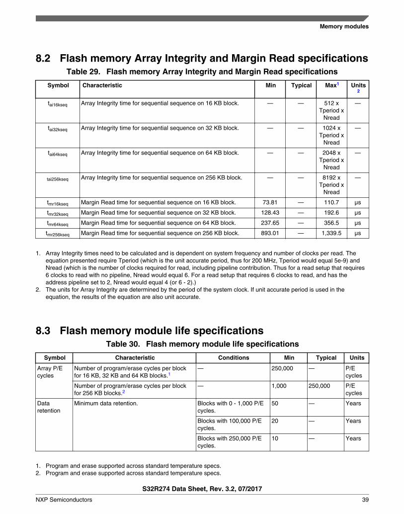
8.2 Flash memory Array Integrity and Margin Read specificationsTable 29. Flash memory Array Integrity and Margin Read specifications
Symbol Characteristic Min Typical Max1 Units2
tai16kseq Array Integrity time for sequential sequence on 16 KB block. — — 512 xTperiod x
Nread
—
tai32kseq Array Integrity time for sequential sequence on 32 KB block. — — 1024 xTperiod x
Nread
—
tai64kseq Array Integrity time for sequential sequence on 64 KB block. — — 2048 xTperiod x
Nread
—
tai256kseq Array Integrity time for sequential sequence on 256 KB block. — — 8192 xTperiod x
Nread
—
tmr16kseq Margin Read time for sequential sequence on 16 KB block. 73.81 — 110.7 μs
tmr32kseq Margin Read time for sequential sequence on 32 KB block. 128.43 — 192.6 μs
tmr64kseq Margin Read time for sequential sequence on 64 KB block. 237.65 — 356.5 μs
tmr256kseq Margin Read time for sequential sequence on 256 KB block. 893.01 — 1,339.5 μs
1. Array Integrity times need to be calculated and is dependent on system frequency and number of clocks per read. Theequation presented require Tperiod (which is the unit accurate period, thus for 200 MHz, Tperiod would equal 5e-9) andNread (which is the number of clocks required for read, including pipeline contribution. Thus for a read setup that requires6 clocks to read with no pipeline, Nread would equal 6. For a read setup that requires 6 clocks to read, and has theaddress pipeline set to 2, Nread would equal 4 (or 6 - 2).)
2. The units for Array Integrity are determined by the period of the system clock. If unit accurate period is used in theequation, the results of the equation are also unit accurate.
8.3 Flash memory module life specificationsTable 30. Flash memory module life specifications
Symbol Characteristic Conditions Min Typical Units
Array P/Ecycles
Number of program/erase cycles per blockfor 16 KB, 32 KB and 64 KB blocks.1
— 250,000 — P/Ecycles
Number of program/erase cycles per blockfor 256 KB blocks.2
— 1,000 250,000 P/Ecycles
Dataretention
Minimum data retention. Blocks with 0 - 1,000 P/Ecycles.
50 — Years
Blocks with 100,000 P/Ecycles.
20 — Years
Blocks with 250,000 P/Ecycles.
10 — Years
1. Program and erase supported across standard temperature specs.2. Program and erase supported across standard temperature specs.
Memory modules
S32R274 Data Sheet, Rev. 3.2, 07/2017
NXP Semiconductors 39
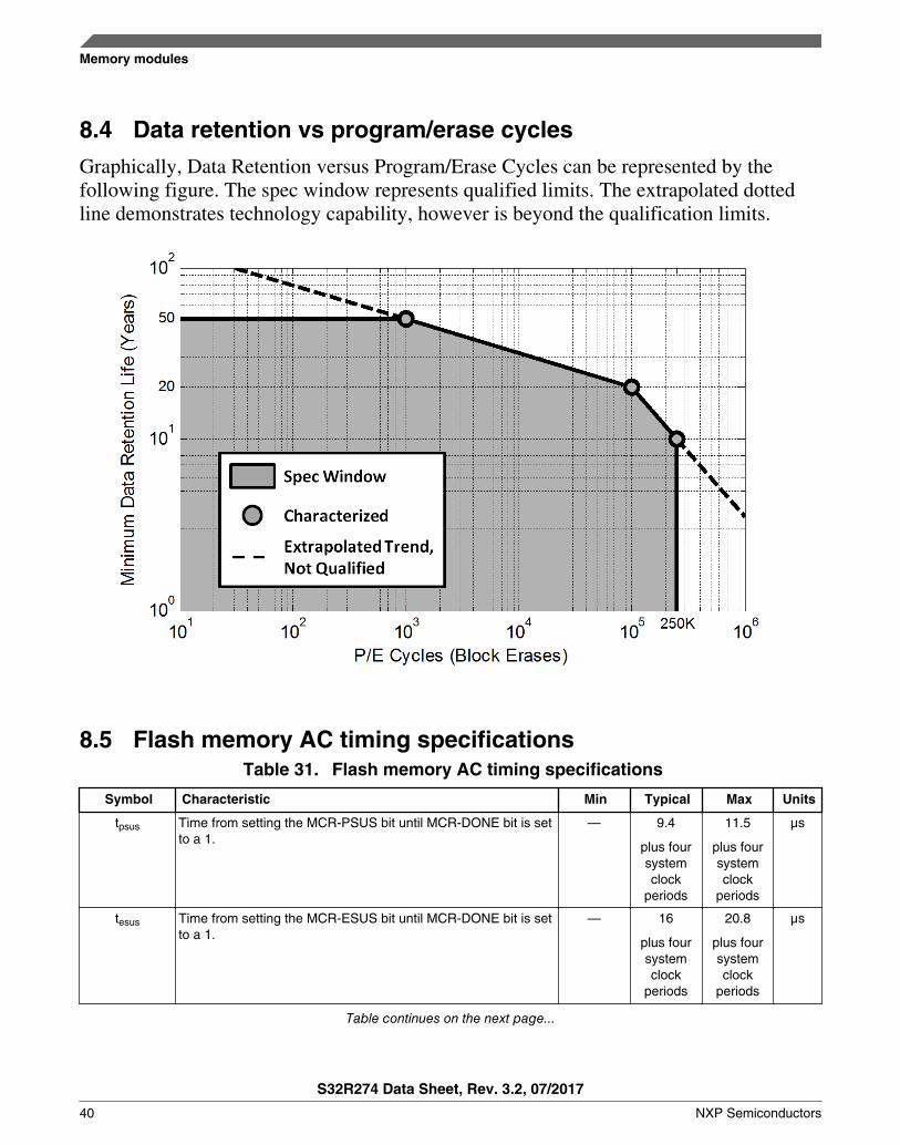
8.4 Data retention vs program/erase cycles
Graphically, Data Retention versus Program/Erase Cycles can be represented by thefollowing figure. The spec window represents qualified limits. The extrapolated dottedline demonstrates technology capability, however is beyond the qualification limits.
8.5 Flash memory AC timing specificationsTable 31. Flash memory AC timing specifications
Symbol Characteristic Min Typical Max Units
tpsus Time from setting the MCR-PSUS bit until MCR-DONE bit is setto a 1.
— 9.4
plus foursystemclock
periods
11.5
plus foursystemclock
periods
μs
tesus Time from setting the MCR-ESUS bit until MCR-DONE bit is setto a 1.
— 16
plus foursystemclock
periods
20.8
plus foursystemclock
periods
μs
Table continues on the next page...
Memory modules
S32R274 Data Sheet, Rev. 3.2, 07/2017
40 NXP Semiconductors

Table 31. Flash memory AC timing specifications (continued)
Symbol Characteristic Min Typical Max Units
tres Time from clearing the MCR-ESUS or PSUS bit with EHV = 1until DONE goes low.
— — 100 ns
tdone Time from 0 to 1 transition on the MCR-EHV bit initiating aprogram/erase until the MCR-DONE bit is cleared.
— — 5 ns
tdones Time from 1 to 0 transition on the MCR-EHV bit aborting aprogram/erase until the MCR-DONE bit is set to a 1.
— 16
plus foursystemclock
periods
20.8
plus foursystemclock
periods
μs
tdrcv Time to recover once exiting low power mode. 16
plus sevensystemclock
periods.
— 45
plus sevensystemclock
periods
μs
taistart Time from 0 to 1 transition of UT0-AIE initiating a Margin Reador Array Integrity until the UT0-AID bit is cleared. This time alsoapplies to the resuming from a suspend or breakpoint byclearing AISUS or clearing NAIBP
— — 5 ns
taistop Time from 1 to 0 transition of UT0-AIE initiating an ArrayIntegrity abort until the UT0-AID bit is set. This time also appliesto the UT0-AISUS to UT0-AID setting in the event of a ArrayIntegrity suspend request.
— — 80
plus fifteensystemclock
periods
ns
tmrstop Time from 1 to 0 transition of UT0-AIE initiating a Margin Readabort until the UT0-AID bit is set. This time also applies to theUT0-AISUS to UT0-AID setting in the event of a Margin Readsuspend request.
10.36
plus foursystemclock
periods
— 20.42
plus foursystemclock
periods
μs
8.6 Flash memory read wait-state and address-pipeline controlsettings
The following table describes the recommended settings of the Flash MemoryController's PFCR1,2,3[RWSC] and PCRC1,2,3[APC] fields at various operatingfrequencies, based on specified intrinsic flash memory access timed of the Flash memory.
Table 32. Flash read wait state and address pipeline control guidelines
Operating frequency(fsys)
RWSC APC Flash read latency onmini-cache miss (# of
sys clock periods)
Flash read latency onmini-cache hit (# ofsys clock periods)
100 MHz 2 1 5 1
120 MHz 3 1 6 1
Memory modules
S32R274 Data Sheet, Rev. 3.2, 07/2017
NXP Semiconductors 41
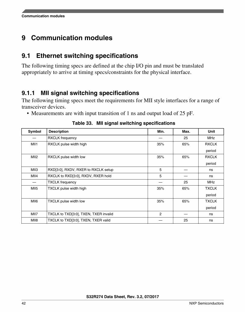
Communication modules
9.1 Ethernet switching specifications
The following timing specs are defined at the chip I/O pin and must be translatedappropriately to arrive at timing specs/constraints for the physical interface.
9.1.1 MII signal switching specificationsThe following timing specs meet the requirements for MII style interfaces for a range oftransceiver devices.
• Measurements are with input transition of 1 ns and output load of 25 pF.
Table 33. MII signal switching specifications
Symbol Description Min. Max. Unit
— RXCLK frequency — 25 MHz
MII1 RXCLK pulse width high 35% 65% RXCLK
period
MII2 RXCLK pulse width low 35% 65% RXCLK
period
MII3 RXD[3:0], RXDV, RXER to RXCLK setup 5 — ns
MII4 RXCLK to RXD[3:0], RXDV, RXER hold 5 — ns
— TXCLK frequency — 25 MHz
MII5 TXCLK pulse width high 35% 65% TXCLK
period
MII6 TXCLK pulse width low 35% 65% TXCLK
period
MII7 TXCLK to TXD[3:0], TXEN, TXER invalid 2 — ns
MII8 TXCLK to TXD[3:0], TXEN, TXER valid — 25 ns
9
Communication modules
S32R274 Data Sheet, Rev. 3.2, 07/2017
42 NXP Semiconductors

MII7MII8
Valid data
Valid data
Valid data
MII6 MII5
TXCLK (input)
TXD[n:0]
TXEN
TXER
Figure 11. MII transmit signal timing diagram
MII2 MII1
MII4MII3
Valid data
Valid data
Valid data
RXCLK (input)
RXD[n:0]
RXDV
RXER
Figure 12. MII receive signal timing diagram
9.1.2 RMII signal switching specificationsThe following timing specs meet the requirements for RMII style interfaces for a range oftransceiver devices.
• Measurements are with input transition of 1 ns and output load of 25 pF.
Table 34. RMII signal switching specifications
Num Description Min. Max. Unit
— EXTAL frequency (RMII input clock RMII_CLK) — 50 MHz
RMII1 RMII_CLK pulse width high 35% 65% RMII_CLKperiod
RMII2 RMII_CLK pulse width low 35% 65% RMII_CLKperiod
RMII3 RXD[1:0], CRS_DV, RXER to RMII_CLK setup 4 — ns
RMII4 RMII_CLK to RXD[1:0], CRS_DV, RXER hold 2 — ns
RMII7 RMII_CLK to TXD[1:0], TXEN invalid 4 — ns
Table continues on the next page...
Communication modules
S32R274 Data Sheet, Rev. 3.2, 07/2017
NXP Semiconductors 43
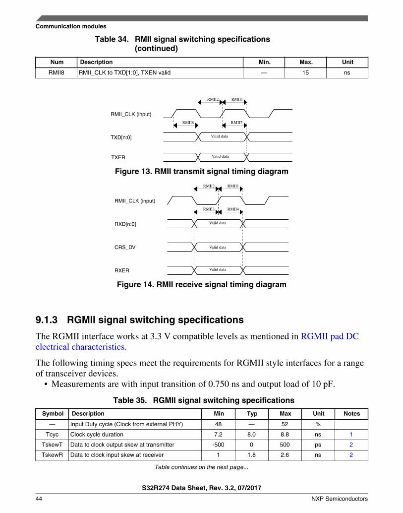
Table 34. RMII signal switching specifications(continued)
Num Description Min. Max. Unit
RMII8 RMII_CLK to TXD[1:0], TXEN valid — 15 ns
RMII7RMII8
Valid data
Valid data
RMII2 RMII1
RMII_CLK (input)
TXD[n:0]
TXER
Figure 13. RMII transmit signal timing diagram
RMII2 RMII1
RMII4RMII3
Valid data
Valid data
Valid data
RMII_CLK (input)
RXD[n:0]
CRS_DV
RXER
Figure 14. RMII receive signal timing diagram
9.1.3 RGMII signal switching specifications
The RGMII interface works at 3.3 V compatible levels as mentioned in RGMII pad DCelectrical characteristics.
The following timing specs meet the requirements for RGMII style interfaces for a rangeof transceiver devices.
• Measurements are with input transition of 0.750 ns and output load of 10 pF.
Table 35. RGMII signal switching specifications
Symbol Description Min Typ Max Unit Notes
— Input Duty cycle (Clock from external PHY) 48 — 52 %
Tcyc Clock cycle duration 7.2 8.0 8.8 ns 1
TskewT Data to clock output skew at transmitter -500 0 500 ps 2
TskewR Data to clock input skew at receiver 1 1.8 2.6 ns 2
Table continues on the next page...
Communication modules
S32R274 Data Sheet, Rev. 3.2, 07/2017
44 NXP Semiconductors

Table 35. RGMII signal switching specifications(continued)
Symbol Description Min Typ Max Unit Notes
Duty_G Duty cycle for Gigabit 45 50 55 % 3
Duty_T Duty cycle for 10/100T 40 50 60 % 3
Tr/Tf Rise/fall time (20–80%) — — 1.5 ns
1. For 10 Mbps and 100 Mbps, Tcyc will scale to 400 ns ±40 ns and 40 ns ±4 ns respectively.2. For all versions of RGMII prior to 2.0; This implies that PC board design will require clocks to be routed such that an
additional trace delay of greater than 1.5 ns and less than 2.0 ns will be added to the associated clock signal. For 10/100the Max value is unspecified.
3. Duty cycle may be stretched/shrunk during speed changes or while transitioning to a received packet's clock domain aslong as minimum duty cycle is not violated and stretching occurs for no more than three Tcyc of the lowest speedtransitioned between.
TskewT
TskewR
TXD[3:0] TXD[8:5]TXD[7:4]
TXD[4]TXEN
TXD[9]TXERR
TXC (at transmitter)
TXD[n:0]
TX_CTL
TXC (at receiver)
Figure 15. RGMII transmit signal timing diagram
TskewT
TskewR
RXD[3:0]RXD[8:5]RXD[7:4]
RXD[4]RXDV
RXD[9]RXERR
RXC (at transmitter)
RXD[n:0]
RX_CTL
RXC (at receiver)
Figure 16. RGMII receive signal timing diagram
Communication modules
S32R274 Data Sheet, Rev. 3.2, 07/2017
NXP Semiconductors 45
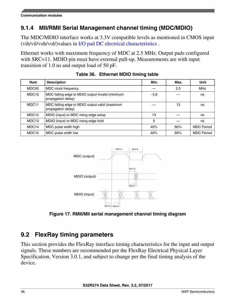
9.1.4 MII/RMII Serial Management channel timing (MDC/MDIO)
The MDC/MDIO interface works at 3.3V compatible levels as mentioned in CMOS input(vih/vil/voh/vol/)values in I/O pad DC electrical characteristics .
Ethernet works with maximum frequency of MDC at 2.5 MHz. Output pads configuredwith SRC=11. MDIO pin must have external pull-up. Measurements are with inputtransition of 1.0 ns and output load of 50 pF.
Table 36. Ethernet MDIO timing table
Num Description Min. Max. Unit
MDC00 MDC clock frequency — 2.5 MHz
MDC10 MDC falling edge to MDIO output invalid (minimumpropagation delay)
- 0.8 — ns
MDC11 MDC falling edge to MDIO output valid (maximumpropagation delay)
— 13 ns
MDC12 MDIO (input) to MDC rising edge setup 13 — ns
MDC13 MDIO (input) to MDC rising edge hold 0 — ns
MDC14 MDC pulse width high 40% 60% MDC Period
MDC15 MDC pulse width low 40% 60% MDC Period
MDC (output)
MDIO (output)
MDIO (input)
MDC10
MDC11
MDC12 MDC13
MDC14 MDC15
Figure 17. RMII/MII serial management channel timing diagram
9.2 FlexRay timing parameters
This section provides the FlexRay interface timing characteristics for the input and outputsignals. These numbers are recommended per the FlexRay Electrical Physical LayerSpecification, Version 3.0.1, and subject to change per the final timing analysis of thedevice.
Communication modules
S32R274 Data Sheet, Rev. 3.2, 07/2017
46 NXP Semiconductors

9.2.1 TxEN
dCCTxENRISEdCCTxENFALL
20 %
80 %
TxEN
Figure 18. FlexRay TxEN signal
Table 37. TxEN output characteristics1
Name Description Min Max Unit
dCCTxENRISE25 Rise time of TxEN signal at CC — 9 ns
dCCTxENFALL25 Fall time of TxEN signal at CC — 9 ns
dCCTxEN01 Sum of delay between Clk to Q of the last FF and the finaloutput buffer, rising edge
— 25 ns
dCCTxEN10 Sum of delay between Clk to Q of the last FF and the finaloutput buffer, falling edge
— 25 ns
1. All parameters specified for VDD_HV_IOx = 3.3 V -5%, +10%, TJ = –40 °C / 150 °C, TxEN pin load maximum 25 pF.
Communication modules
S32R274 Data Sheet, Rev. 3.2, 07/2017
NXP Semiconductors 47

dCCTxEN10 dCCTxEN01
TxEN
PE_Clk
Figure 19. FlexRay TxEN signal propagation delays
9.2.2 TxD
dCCTxD50%
TxD
dCCTxDFALL dCCTxDRISE
20 %
50 %
80 %
Figure 20. FlexRay TxD signal
• Measurements are with output load of 25 pF and pad configured as SRE =11.
Table 38. TxD output characteristics
Name Description1 Min Max Unit
dCCTxAsym Asymmetry of sending CC @ 25 pF load –2.45 2.45 ns
Table continues on the next page...
Communication modules
S32R274 Data Sheet, Rev. 3.2, 07/2017
48 NXP Semiconductors
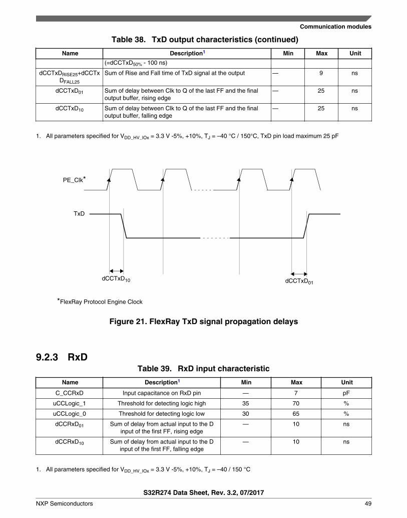
Table 38. TxD output characteristics (continued)
Name Description1 Min Max Unit
(=dCCTxD50% - 100 ns)
dCCTxDRISE25+dCCTxDFALL25
Sum of Rise and Fall time of TxD signal at the output — 9 ns
dCCTxD01 Sum of delay between Clk to Q of the last FF and the finaloutput buffer, rising edge
— 25 ns
dCCTxD10 Sum of delay between Clk to Q of the last FF and the finaloutput buffer, falling edge
— 25 ns
1. All parameters specified for VDD_HV_IOx = 3.3 V -5%, +10%, TJ = –40 °C / 150°C, TxD pin load maximum 25 pF
dCCTxD10 dCCTxD01
TxD
PE_Clk*
*FlexRay Protocol Engine Clock
Figure 21. FlexRay TxD signal propagation delays
9.2.3 RxDTable 39. RxD input characteristic
Name Description1 Min Max Unit
C_CCRxD Input capacitance on RxD pin — 7 pF
uCCLogic_1 Threshold for detecting logic high 35 70 %
uCCLogic_0 Threshold for detecting logic low 30 65 %
dCCRxD01 Sum of delay from actual input to the Dinput of the first FF, rising edge
— 10 ns
dCCRxD10 Sum of delay from actual input to the Dinput of the first FF, falling edge
— 10 ns
1. All parameters specified for VDD_HV_IOx = 3.3 V -5%, +10%, TJ = –40 / 150 °C
Communication modules
S32R274 Data Sheet, Rev. 3.2, 07/2017
NXP Semiconductors 49

9.2.4 Receiver asymmetryTable 40. Receiver asymmetry
Name Description Min Max Unit
dCCRxAsymAccept15 Acceptance of asymmetry at receiving CC with 15 pF load (*) –31.5 +44.0 ns
dCCRxAsymAccept25 Acceptance of asymmetry at receiving CC with 25 pF load (*) –30.5 +43.0 ns
9.3 LVDS Fast Asynchronous Transmission (LFAST) electricalcharacteristics
The following table provides output driver characteristics for LFAST I/Os.
Table 41. LFAST output buffer electrical characteristics
Symbol Parameter Conditions1 Value Unit
Min Typ Max
|ΔVO_L| Absolute value for differential outputvoltage swing (terminated)
— 100 200 285 mV
VICOM_L Common mode voltage — 1.08 1.2 1.32 V
Ttr_L Transition time output pin LVDSconfiguration
— 0.2 — 1.5 ns
1. VDD_HV_IOx = 3.3 V (–5%, +10%), TJ = –40 / 150 °C, unless otherwise specified.
NOTEFast IOs must be specified only as fast (and not as highcurrent). See GPIO DC electrical specification.
Communication modules
S32R274 Data Sheet, Rev. 3.2, 07/2017
50 NXP Semiconductors

9.3.1 LFAST interface timing diagrams
Figure 22. LFAST timing definition
Communication modules
S32R274 Data Sheet, Rev. 3.2, 07/2017
NXP Semiconductors 51

Data Validpad_p/pad_nDifferential TXData Lines
H
L
Tsu
lfast_pwr_down
Figure 23. Power-down exit time
Differential TXData Lines
pad_p/pad_n
TriseTfall
90%
10%
VIH
VIL
Figure 24. Rise/fall time
9.3.2 LFAST interface electrical characteristics
NOTEWhile LFAST is operating and 'Ready' (nex_rdy_b) signal isused by the debugger on PAD_132, the recommended SREsettings are ‘00' and ‘01'. TCK should be used with lowfrequency (preferably less than 10 MHz).
Table 42. LFAST electrical characteristics
Symbol Parameter Conditions1 Value Unit
Min Typ Max
Data Rate
DATARATE Data rate — — 312/320 Typ+0.1% Mbps
STARTUP
TSTRT_BIAS Bias startup time2 — — 0.5 3 µs
Table continues on the next page...
Communication modules
S32R274 Data Sheet, Rev. 3.2, 07/2017
52 NXP Semiconductors

Table 42. LFAST electrical characteristics(continued)
Symbol Parameter Conditions1 Value Unit
Min Typ Max
TPD2NM_TX Transmitter startup time(power down to normal
mode)3
— — 0.2 2 µs
TSM2NM_TX Transmitter startup time(sleep mode to normal
mode)4
— — 0.2 0.5 µs
TPD2NM_RX Receiver startup time5
(Power down to Normalmode)
— — 20 40 ns
TPD2SM_RX Receiver startup time4
(Power down to Sleepmode)
— — 20 50 ns
TRANSMITTER
VOS_DRF Common mode voltage — 1.08 — 1.32 V
|ΔVOD_DRF| Differential output voltageswing (terminated)
— ±100 ±200 ± 285 mV
TTR_DRF Rise/Fall time (10% - 90% ofswing)
— 0.26 — 1.5 ns
ROUT_DRF Terminating resistance 67 — 198 Ω
COUT_DRF Capacitance6 — — — 5 pF
RECEIVER
VICOM_DRF Common mode voltage — 0.157 — 1.68 V
|DVI_DRF| Differential input voltage — 100 — — mV
VHYS_DRF Input hysteresis — 25 — — mV
RIN_DRF Terminating resistance 80 115 150 Ω
CIN_DRF Capacitance9 — — 3.5 6 pF
LIN_DRF Parasitic Inductance10 — — 5 10 nH
TRANSMISSION LINE CHARACTERISTICS (PCB Track)
Z0 Transmission linecharacteristic impedance
— 47.5 50 52.5 Ω
ZDIFF Transmission line differentialimpedance
— 95 100 105 Ω
1. VDD_VH_IOx = 3.3 V -5%,+10%, TJ = –40 / 150 °C, unless otherwise specified2. Startup time is defined as the time taken by LFAST current reference block for settling bias current after its pwr_down
(power down) has been deasserted. LFAST functionality is guaranteed only after the startup time.3. Startup time is defined as the time taken by LFAST transmitter for settling after its pwr_down (power down) has been
deasserted. Here it is assumed that current reference is already stable. LFAST functionality is guaranteed only after thestartup time.
4. Startup time is defined as the time taken by LFAST transmitter for settling after its pwr_down (power down) has beendeasserted. Here it is assumed that current reference is already stable. LFAST functionality is guaranteed only after thestartup time.
5. Startup time is defined as the time taken by LFAST receiver for settling after its pwr_down (power down) has beendeasserted. Here it is assumed that current reference is already stable. LFAST functionality is guaranteed only after thestartup time.
Communication modules
S32R274 Data Sheet, Rev. 3.2, 07/2017
NXP Semiconductors 53

6. Total lumped capacitance including silicon, package pin and bond wire. Application board simulation is needed to verifyLFAST template compliancy.
7. Absolute min = 0.15 V – (285 mV / 2) = 0 V8. Absolute max = 1.6 V + (285 mV / 2) = 1.743 V9. Total capacitance including silicon, package pin and bond wire10. Total inductance including silicon, package pin and bond wire
9.4 Serial Peripheral Interface (SPI) timing specifications
The following table describes the SPI electrical characteristics.
MTEF=1 Mode timing values given below are only applicable when external SPI is inclassic mode. Slave mode timing values given below are applicable when device is inMTFE=0.
• Measurements are with maximum output load of 50 pF, input transition of 1 ns andpad configured as SRE = 11.
Table 43. SPI timing
No. Symbol Parameter Conditions Min Max Unit
1 tSCK SPI cycle time Master (MTFE = 0) 50 — ns
Master (MTFE = 1) 50 —
Slave (MTFE = 0) 50 —
Slave Receive Only mode1 16 —
2 tCSC PCS to SCK delay Master 63.82 — ns
3 tASC After SCK delay Master 68.83 — ns
4 tSDC SCK duty cycle Master4 tSCK/2 – 1 tSCK/2 + 1 ns
Slave5 — — ns
Slave Receive only mode6 tSCK/2 –0.750
tSCK/2 +0.750
ns
5 tA Slave access time SS active to SOUT valid — 25 ns
6 tDIS Slave SOUT disable time SS inactive to SOUT High-Z or invalid — 25 ns
7 tPCSC PCSx to PCSS time — 13 7 — ns
8 tPASC PCSS to PCSx time — 13 8 — ns
9 tSUI Data setup time for inputs Master (MTFE = 0) 15 — ns
Slave 2 —
Slave Receive Mode 2 —
Master (MTFE = 1, CPHA = 0)9 15-N x SPIIPG clockperiod10
—
Master (MTFE = 1, CPHA = 1) 15 —
10 tHI Data hold time for inputs Master (MTFE = 0) –2 — ns
Slave 4 —
Slave Receive Mode 4 —
Table continues on the next page...
Communication modules
S32R274 Data Sheet, Rev. 3.2, 07/2017
54 NXP Semiconductors

Table 43. SPI timing (continued)
No. Symbol Parameter Conditions Min Max Unit
Master (MTFE = 1, CPHA = 0)9 -2 + N x SPIIPG clockperiod 10
—
Master (MTFE = 1, CPHA = 1) –2 —
11 tSUO Data valid (after SCK edge) Master (MTFE = 0) — 7 11 ns
Slave — 23
Master (MTFE = 1, CPHA = 0)12 — 7 + SPI IPGClock Period
Master (MTFE = 1, CPHA = 1) — 7
12 tHO Data hold time for outputs Master (MTFE = 0) –4 11 — ns
Slave 3.8 —
Master (MTFE = 1, CPHA = 0) 12 -4 + SPI IPGClock Period
—
Master (MTFE = 1, CPHA = 1) –4 —
1. Slave Receive Only mode can operate at a maximum frequency of 60 MHz. In this mode, the SPI can receive data on SIN,but no valid data is transmitted on SOUT.
2. For SPI_CTARn[PCSSCK] - 'PCS to SCK Delay Prescaler' configuration is '3' (01h) and SPI_CTARn[CSSCK] - 'PCS toSCK Delay Scaler' configuration is '2' (0000h).
3. For SPI_CTARn[PASC] - 'After SCK Delay Prescaler' configuration is '3' (01h) and SPI_CTARn[ASC] - 'After SCK DelayScaler' configuration is '2' (0000h).
4. The numbers are valid when SPI is configured for 50/50. Refer the Reference manual for the mapping of the duty cycle toeach configuration. A change in duty cycle changes the parameter here. For example, a configuration providing duty cycleof 33/66 at SPI translates to min tSCK/3 - 1.5 ns and max tSCK/3 + 1.5 ns.
5. The slave mode parameters (tSUI, tHI, tSUO and tHO) assume 50% duty cycle on SCK input. Any change in SCK duty cycleinput must be taken care during the board design or by the master timing.
6. The slave receive only mode parameters (tSUI and tHI) assume 50% duty cycle on SCK input. Any change in SCK dutycycle input must be taken care during the board design or by the master timing. However, there is additional restriction inthe slave receive only mode that the duty cycle at the slave input should not go below tsdc(min) corresponding to thetsdc(min) for the slave receive mode.
7. In the master mode, this is governed by tPCSSCK. Refer the SPI chapter in the Reference Manual for details. The minimumspec is valid only for SPI_CTARn[PCSSCK]= '0b01' (PCS to SCK delay prescalar of 3) or higher.
8. In the master mode, this is governed by tPASC. Refer the SPI chapter in the Reference Manual for details. The minimumspec is valid only for SPI_CTARn[PASC]= '0b01' (after SCK delay prescalar of 3) or higher.
9. For SPI_CTARn[BR] - 'Baud Rate Scaler' configuration is >= 4.10. N = Configured sampling point value in MTFE=1 Mode.11. Same value is applicable for PCS timing in continuous SCK mode.12. SPI_MCR[SMPL_PT] should be set to 1.
NOTEFor numbers shown in the following figures, see Table 43.
Communication modules
S32R274 Data Sheet, Rev. 3.2, 07/2017
NXP Semiconductors 55

Data Last DataFirst Data
First Data Data Last Data
SIN
SOUT
PCSx
SCK Output
4
9
12
1
11
10
4
SCK Output
(CPOL=0)
(CPOL=1)
32
Figure 25. SPI classic SPI timing — master, CPHA = 0
Data Last DataFirst DataSIN
SOUT
12 11
10
Last DataDataFirst Data
SCK Output
SCK Output
PCSx
9
(CPOL=0)
(CPOL=1)
Figure 26. SPI classic SPI timing — master, CPHA = 1
Communication modules
S32R274 Data Sheet, Rev. 3.2, 07/2017
56 NXP Semiconductors
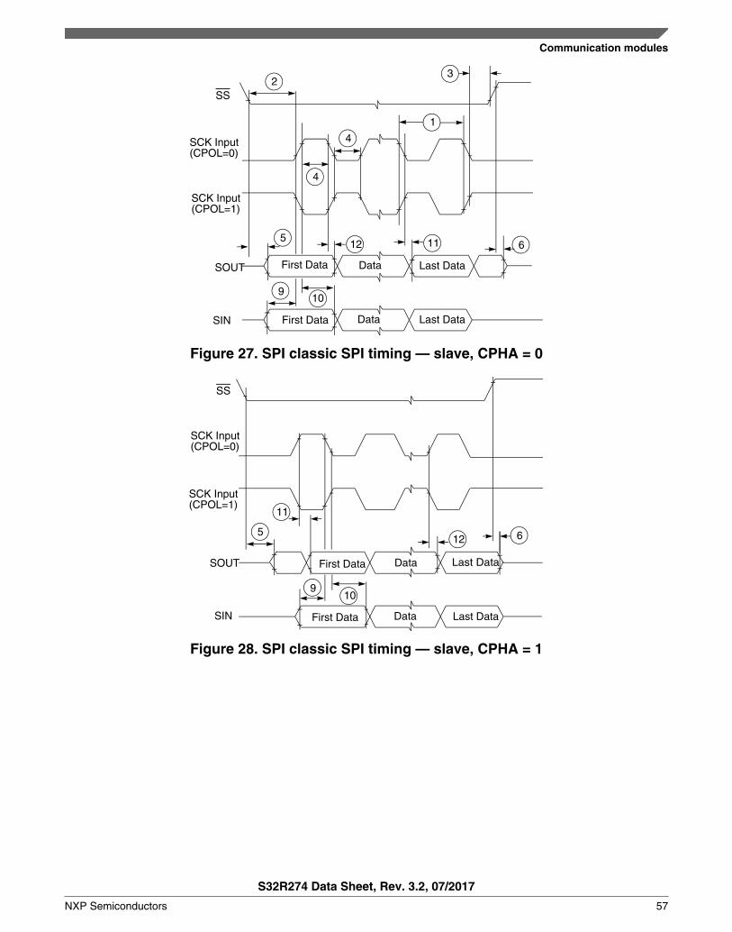
Last DataFirst Data
3
4
1
Data
Data
SIN
SOUT
SS
4
5 6
9
11
10
12
SCK Input
First Data Last Data
SCK Input
2
(CPOL=0)
(CPOL=1)
Figure 27. SPI classic SPI timing — slave, CPHA = 0
5 6
9
12
11
10
Last Data
Last DataSIN
SOUT
SS
First Data
First Data
Data
Data
SCK Input
SCK Input
(CPOL=0)
(CPOL=1)
Figure 28. SPI classic SPI timing — slave, CPHA = 1
Communication modules
S32R274 Data Sheet, Rev. 3.2, 07/2017
NXP Semiconductors 57
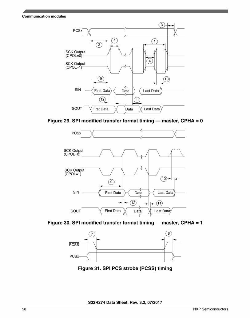
PCSx
3
14
10
4
9
12 11
SCK Output
SCK Output
SIN
SOUT
First Data Data Last Data
First Data Data Last Data
2
(CPOL=0)
(CPOL=1)
Figure 29. SPI modified transfer format timing — master, CPHA = 0
PCSx
109
12 11
SCK Output
SCK Output
SIN
SOUT
First Data Data Last Data
First Data Data Last Data
(CPOL=0)
(CPOL=1)
Figure 30. SPI modified transfer format timing — master, CPHA = 1
PCSx
7 8
PCSS
Figure 31. SPI PCS strobe (PCSS) timing
Communication modules
S32R274 Data Sheet, Rev. 3.2, 07/2017
58 NXP Semiconductors

9.5 LINFlexD timing specifications
The maximum bit rate is 1.875 MBit/s.
9.6 I2C timingTable 44. I2C SCL and SDA input timing specifications
Number Symbol Parameter Value Unit
Min Max
1 I_tHD:STA Start Condition hold time 2 -Peripheral clock2 I_t_LOW Clock low time 8 -
3 I_tHD:DAT Data hold time 2 -
4 I_tHIGH Clock high time 4 -
5 I_tSU:DAT Data setup time 4 -
6 I_tSU:STA Start condition setup time (for repeatedstart condition only)
2 -
7 I_tSU:STOP Stop condition setup time 2 -
Table 45. I2C SCL and SDA output timing specifications
Number Symbol Parameter Value Unit
Min Max
1 O_tHD:STA Start condition hold time1 6 -
Peripheral clock
2 O_t_LOW Clock low time1 10 -
3 O_tHD:DAT Data hold time1 7 -
4 O_t_HIGH Clock high time1 10 -
5 O_tSU:DAT Data setup time1 2 -
6 O_tSU:STA Start condition setup time (forrepeated start condition only)1
20 -
7 O_tSU:STOP Stop condition setup time1 10 -
8 O_tr SCL/SDA rise time2 - 99.6 ns
9 O_tf SCL/SDA fall time1 - 99.6
1. Programming IBFD (I2C Bus Frequency Divider Register) with the maximum frequency results in the minimum outputtimings listed. The I2C interface is designed to scale the data transition time, moving it to the middle of the SCL low period.The actual position is affected by the prescale and division values programmed in IBDR (I2C Bus Data I/O Register).
2. Serial data (SDA) and Serial clock (SCL) reaches peak level depending upon the external signal capacitance and pull upresistor values as SDA and SCL are open-drain type outputs which are only actively driven low by the I2C module.
Communication modules
S32R274 Data Sheet, Rev. 3.2, 07/2017
NXP Semiconductors 59

Figure 32. I2C input/output timing
Debug modules
10.1 JTAG/CJTAG interface timingThe following table lists JTAGC/CJTAG electrical characteristics.
• Measurements are with input transition of 1 ns, output load of 50 pF and padsconfigured with SRE=11.
Table 46. JTAG/CJTAG pin AC electrical characteristics 1
# Symbol Characteristic Min Max Unit
1 tJCYC2 TCK Cycle Time (JTAG) 36 — ns
TCK Cycle Time (CJTAG) 50
2 tJDC TCK Clock Pulse Width 40 60 %
3 tTCKRISE TCK Rise and Fall Times (40% - 70%) — 3 ns
4 tTMSS, tTDIS TMS, TDI Data Setup Time 5 — ns
5 tTMSH, tTDIH TMS, TDI Data Hold Time 5 — ns
6 tTDOV TCK Low to TDO/TMS Data Valid 3 — 154 ns
7 tTDOI TCK Low to TDO/TMS Data Invalid3 0 — ns
8 tTDOHZ TCK Low to TDO/TMS High Impedance3 — 22 ns
9 tJCMPPW JCOMP Assertion Time 100 — ns
10 tJCMPS JCOMP Setup Time to TCK Low 40 — ns
11 tBSDV TCK Falling Edge to Output Valid — 6005 ns
12 tBSDVZ TCK Falling Edge to Output Valid out of HighImpedance
— 600 ns
13 tBSDHZ TCK Falling Edge to Output High Impedance — 600 ns
14 tBSDST Boundary Scan Input Valid to TCK Rising Edge 15 — ns
Table continues on the next page...
10
Debug modules
S32R274 Data Sheet, Rev. 3.2, 07/2017
60 NXP Semiconductors
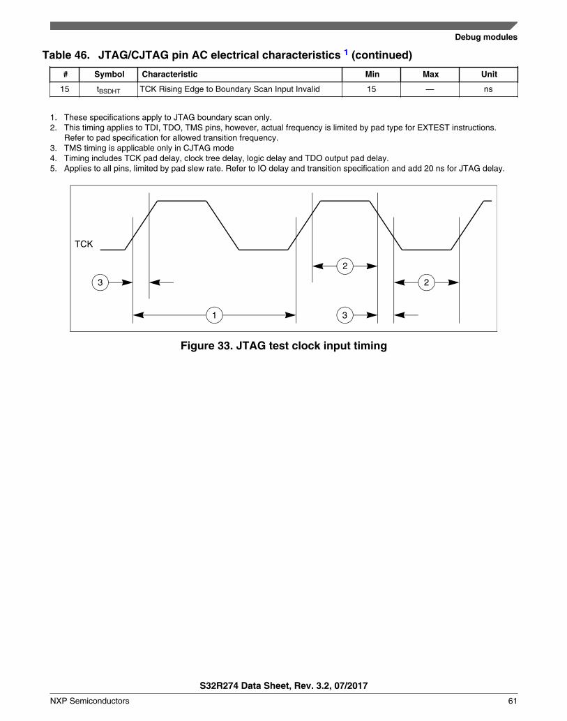
Table 46. JTAG/CJTAG pin AC electrical characteristics 1 (continued)
# Symbol Characteristic Min Max Unit
15 tBSDHT TCK Rising Edge to Boundary Scan Input Invalid 15 — ns
1. These specifications apply to JTAG boundary scan only.2. This timing applies to TDI, TDO, TMS pins, however, actual frequency is limited by pad type for EXTEST instructions.
Refer to pad specification for allowed transition frequency.3. TMS timing is applicable only in CJTAG mode4. Timing includes TCK pad delay, clock tree delay, logic delay and TDO output pad delay.5. Applies to all pins, limited by pad slew rate. Refer to IO delay and transition specification and add 20 ns for JTAG delay.
TCK
1
2
2
3
3
Figure 33. JTAG test clock input timing
Debug modules
S32R274 Data Sheet, Rev. 3.2, 07/2017
NXP Semiconductors 61
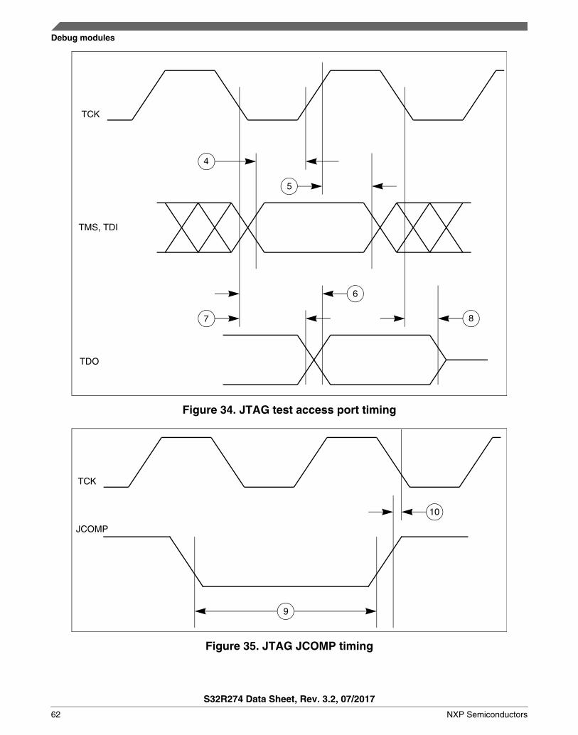
TCK
4
5
6
7 8
TMS, TDI
TDO
Figure 34. JTAG test access port timing
TCK
JCOMP
9
10
Figure 35. JTAG JCOMP timing
Debug modules
S32R274 Data Sheet, Rev. 3.2, 07/2017
62 NXP Semiconductors

TCK
OutputSignals
InputSignals
OutputSignals
11
12
13
14
15
Figure 36. JTAG boundary scan timing
10.2 Nexus Aurora debug port timingTable 47. Nexus Aurora debug port timing
# Symbol Characteristic Min Max Unit
1 tREFCLK Reference clock frequency 625 1250 MHz
1a tMCYC Reference Clock rise/fall time — 400 ps
2 tRCDC Reference Clock Duty Cycle 45 55 %
3 JRC Reference Clock jitter — 40 ps
4 tSTABILITY Reference Clock Stability 50 — PPM
5 BER Bit Error Rate — 10-12 —
6 JD Transmit lane Deterministic Jitter — 0.17 OUI
7 JT Transmit lane Total Jitter — 0.35 OUI
8 SO Differential output skew — 20 ps
Table continues on the next page...
Debug modules
S32R274 Data Sheet, Rev. 3.2, 07/2017
NXP Semiconductors 63
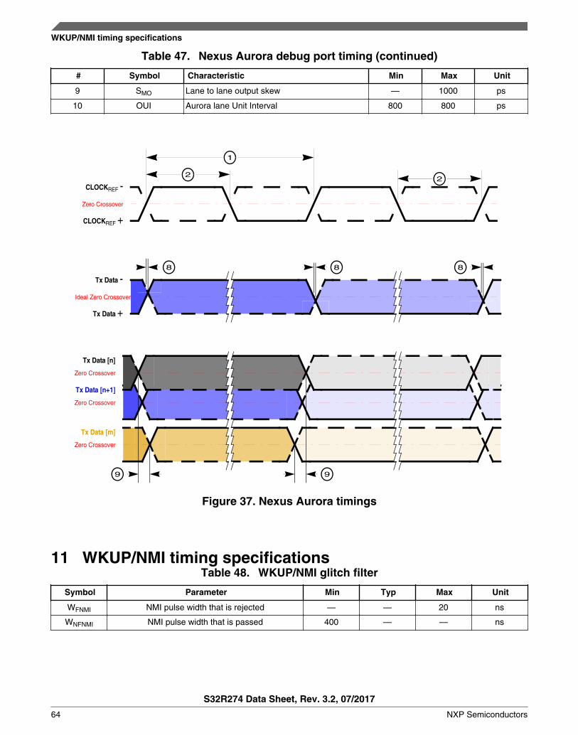
Table 47. Nexus Aurora debug port timing (continued)
# Symbol Characteristic Min Max Unit
9 SMO Lane to lane output skew — 1000 ps
10 OUI Aurora lane Unit Interval 800 800 ps
Tx Data [m]
Zero Crossover
CLOCKREF -
CLOCKREF +
2
Zero Crossover
2
1
Tx Data -
Tx Data +
Ideal Zero Crossover
Tx Data [n]
Zero Crossover
Tx Data [n+1]
Zero Crossover
99
88 8
Figure 37. Nexus Aurora timings
11 WKUP/NMI timing specificationsTable 48. WKUP/NMI glitch filter
Symbol Parameter Min Typ Max Unit
WFNMI NMI pulse width that is rejected — — 20 ns
WNFNMI NMI pulse width that is passed 400 — — ns
WKUP/NMI timing specifications
S32R274 Data Sheet, Rev. 3.2, 07/2017
64 NXP Semiconductors

12 External interrupt timing (IRQ pin)Table 49. External interrupt timing
No. Symbol Parameter Conditions Min Max Unit
1 tIPWL IRQ pulse width low — 3 — tCYC
2 tIPWH IRQ pulse width high — 3 — tCYC
3 tICYC IRQ edge to edge time1 — 6 — tCYC
1. Applies when IRQ pins are configured for rising edge or falling edge events, but not both
NOTEtCYC is equivalent to TCK (prescaled filter clock period)which is the IRC clock prescaled to the Interrupt Filter ClockPrescaler (IFCP) value. TCK = T(IRC) x (IFCP + 1) whereT(IRC) is the internal oscillator period. Refer SIUL2 chapter ofthe device reference manual for details.
IRQ
1
2
3
Figure 38. External interrupt timing
13 Temperature sensor electrical characteristicsThe following table describes the temperature sensor electrical characteristics.
Table 50. Temperature sensor electrical characteristics
Symbol Parameter Conditions Min Typ Max Unit
— Temperature monitoring range -40 — 150 °C
TSENS Sensitivity — 5.18 — mV/°C
TACC Accuracy TJ = -40 to 150°C 5 — 5 °C
External interrupt timing (IRQ pin)
S32R274 Data Sheet, Rev. 3.2, 07/2017
NXP Semiconductors 65

Radar module
14.1 MIPICSI2 D-PHY electrical and timing specifications
This section describes MIPICSI21 D-PHY electrical specifications, compliant withMIPICSI2 version 1.1, D-PHY specification Rev. 1.0 (for MIPI sensor port x4 lanes).
15 kΩ(+/-1%)
REXT
Figure 39. MIPICSI2 circuit
Table 51. Calibrator specifications
Symbol Parameters Min Typ Max Unit
REXT External reference resistor, 1% accuracy (or better), for autocalibration
- 15 - kΩ
Tcal Time from when PD signal goes low to when CALCOMPL goes high - 2 2.5 μs
14.1.1 Electrical and timing informationTable 52. Electrical and timing information
Symbol Parameters Min Typ Max Unit
HS Line Receiver DC Specifications
VIDTH Differential input high voltage threshold - - 70 mV
VIDTL Differential input low voltage threshold -70 - - mV
VIHHS Single ended input high voltage - - 460 mV
VILHS Single ended input low voltage -40 - - mV
VCMRXDC Input common mode voltage 70 - 330 mV
VTERM-EN Single-ended threshold for HS terminationenable
- - 450 mV
ZID Differential input impedance 80 - 125 ohm
LP Line Receiver DC Specifications
VILLP Input low voltage - - 550 mV
Table continues on the next page...
14
1. All rights reserved. This material is reprinted with the permission of the MIPI Alliance, Inc. No part(s) of this document maybe disclosed, reproduced or used for any purpose other than as needed to support the use of the products of NXPSemiconductors.
Radar module
S32R274 Data Sheet, Rev. 3.2, 07/2017
66 NXP Semiconductors
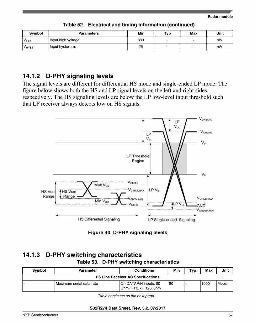
Table 52. Electrical and timing information (continued)
Symbol Parameters Min Typ Max Unit
VIHLP Input high voltage 880 - - mV
VHYST Input hysteresis 25 - - mV
14.1.2 D-PHY signaling levelsThe signal levels are different for differential HS mode and single-ended LP mode. Thefigure below shows both the HS and LP signal levels on the left and right sides,respectively. The HS signaling levels are below the LP low-level input threshold suchthat LP receiver always detects low on HS signals.
Figure 40. D-PHY signaling levels
14.1.3 D-PHY switching characteristicsTable 53. D-PHY switching characteristics
Symbol Parameter Conditions Min Typ Max Unit
HS Line Receiver AC Specifications
- Maximum serial data rate On DATAP/N inputs. 80Ohm<= RL <= 125 Ohm
80 - 1000 Mbps
Table continues on the next page...
Radar module
S32R274 Data Sheet, Rev. 3.2, 07/2017
NXP Semiconductors 67

Table 53. D-PHY switching characteristics (continued)
Symbol Parameter Conditions Min Typ Max Unit
ΔVCMRX(HF) Common mode interference beyond450 MHz
- - 100 mVpp
ΔVCMRX(LF) Common mode interference between50 MHz and 450 MHz
-50 - 50 mVpp
CCM Common mode termination - - 60 pF
LP Line Receiver AC Specification
eSPIKE Input pulse rejection - - 300 Vps
T MIN Minimum pulse response 20 - - ns
VINT Pk-to-Pk interference voltage - - 200 mV
fINT Interference frequency 450 - - MHz
14.1.4 Low-power receiver timing
Figure 41. Input Glitch Rejection of Low-Power Receivers
Radar module
S32R274 Data Sheet, Rev. 3.2, 07/2017
68 NXP Semiconductors

14.1.5 Data to clock timing
Figure 42. Definition
Table 54. Data to clock timing specifications
Symbol Parameter Min Typ Max Unit
TCLKP Clock Period 40 - 500 MHz
UIINST UI Instantaneuous 1 - 12.5 ns
TSETUP Data to Clock Setup Time 0.15 - - UIINST
THOLD Clock to Data Hold Time 0.15 - - UIINST
14.2 MIPICSI2 Disclaimer
The material contained herein is not a license, either expressly or impliedly, to any IPRowned or controlled by any of the authors or developers of this material or MIPI®. Thematerial contained herein is provided on an “AS IS” basis and to the maximum extentpermitted by applicable law, this material is provided AS IS AND WITH ALL FAULTS,and the authors and developers of this material and MIPI hereby disclaim all otherwarranties and conditions, either express, implied or statutory, including, but not limitedto, any (if any) implied warranties, duties or conditions of merchantability, of fitness for aparticular purpose, of accuracy or completeness of responses, of results, of workmanlikeeffort, of lack of viruses, and of lack of negligence.
Radar module
S32R274 Data Sheet, Rev. 3.2, 07/2017
NXP Semiconductors 69

All materials contained herein are protected by copyright laws, and may not bereproduced, republished, distributed, transmitted, displayed, broadcast or otherwiseexploited in any manner without the express prior written permission of MIPI Alliance.MIPI, MIPI Alliance and the dotted rainbow arch and all related trademarks, trade names,and other intellectual property are the exclusive property of MIPI Alliance and cannot beused without its express prior written permission.
ALSO, THERE IS NO WARRANTY OF CONDITION OF TITLE, QUIETENJOYMENT, QUIET POSSESSION, CORRESPONDENCE TO DESCRIPTION ORNON-INFRINGEMENT WITH REGARD TO THIS MATERIAL OR THE CONTENTSOF THIS DOCUMENT. IN NO EVENT WILL ANY AUTHOR OR DEVELOPER OFTHIS MATERIAL OR THE CONTENTS OF THIS DOCUMENT OR MIPI BELIABLE TO ANY OTHER PARTY FOR THE COST OF PROCURING SUBSTITUTEGOODS OR SERVICES, LOST PROFITS, LOSS OF USE, LOSS OF DATA, OR ANYINCIDENTAL, CONSEQUENTIAL, DIRECT, INDIRECT, OR SPECIAL DAMAGESWHETHER UNDER CONTRACT, TORT, WARRANTY, OR OTHERWISE,ARISING IN ANY WAY OUT OF THIS OR ANY OTHER AGREEMENT,SPECIFICATION OR DOCUMENT RELATING TO THIS MATERIAL, WHETHEROR NOT SUCH PARTY HAD ADVANCE NOTICE OF THE POSSIBILITY OFSUCH DAMAGES.
Without limiting the generality of this Disclaimer stated above, the user of the contents ofthis Document is further notified that MIPI: (a) does not evaluate, test or verify theaccuracy, soundness or credibility of the contents of this Document; (b) does not monitoror enforce compliance with the contents of this Document; and (c) does not certify, test,or in any manner investigate products or services or any claims of compliance with thecontents of this Document. The use or implementation of the contents of this Documentmay involve or require the use of intellectual property rights ("IPR") including (but notlimited to) patents, patent applications, or copyrights owned by one or more parties,whether or not Members of MIPI. MIPI does not make any search or investigation forIPR, nor does MIPI require or request the disclosure of any IPR or claims of IPR asrespects the contents of this Document or otherwise.
Radar module
S32R274 Data Sheet, Rev. 3.2, 07/2017
70 NXP Semiconductors
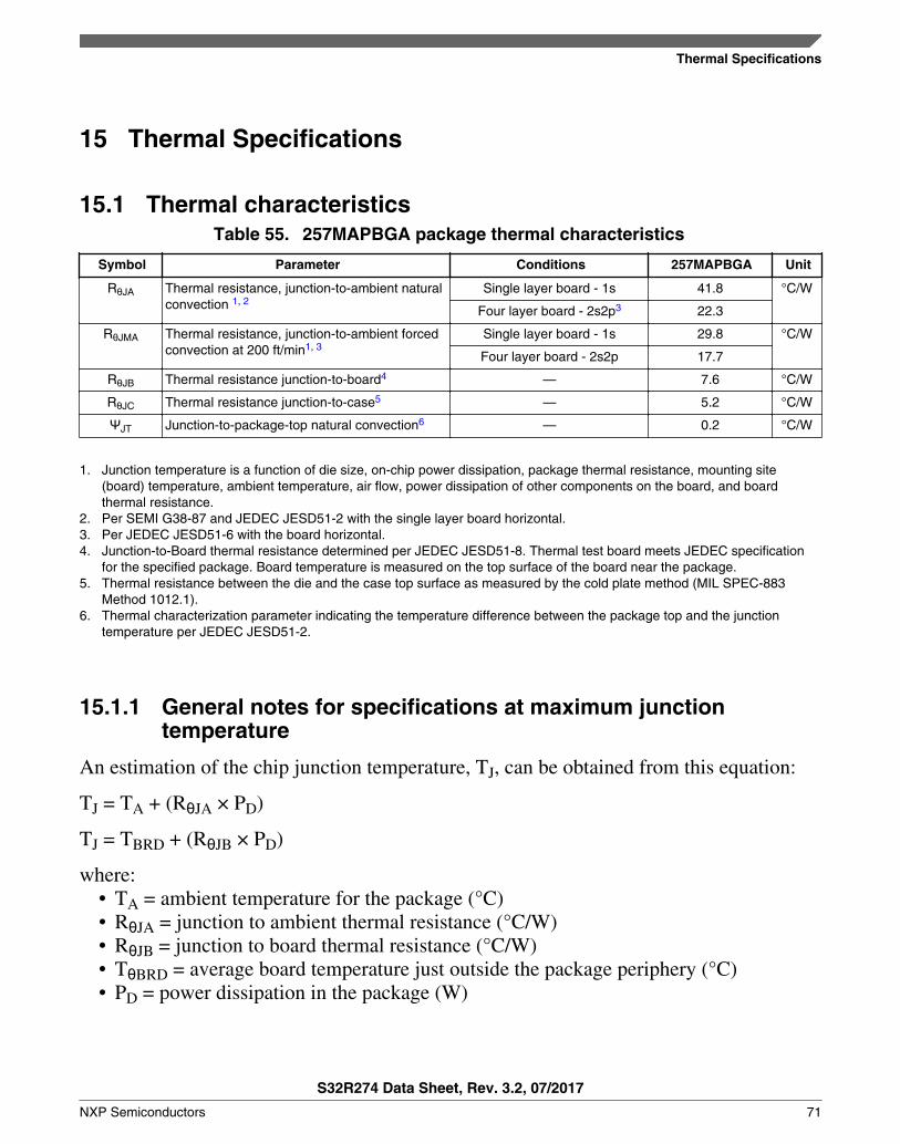
Thermal Specifications
15.1 Thermal characteristicsTable 55. 257MAPBGA package thermal characteristics
Symbol Parameter Conditions 257MAPBGA Unit
RθJA Thermal resistance, junction-to-ambient naturalconvection 1, 2
Single layer board - 1s 41.8 °C/W
Four layer board - 2s2p3 22.3
RθJMA Thermal resistance, junction-to-ambient forcedconvection at 200 ft/min1, 3
Single layer board - 1s 29.8 °C/W
Four layer board - 2s2p 17.7
RθJB Thermal resistance junction-to-board4 — 7.6 °C/W
RθJC Thermal resistance junction-to-case5 — 5.2 °C/W
ΨJT Junction-to-package-top natural convection6 — 0.2 °C/W
1. Junction temperature is a function of die size, on-chip power dissipation, package thermal resistance, mounting site(board) temperature, ambient temperature, air flow, power dissipation of other components on the board, and boardthermal resistance.
2. Per SEMI G38-87 and JEDEC JESD51-2 with the single layer board horizontal.3. Per JEDEC JESD51-6 with the board horizontal.4. Junction-to-Board thermal resistance determined per JEDEC JESD51-8. Thermal test board meets JEDEC specification
for the specified package. Board temperature is measured on the top surface of the board near the package.5. Thermal resistance between the die and the case top surface as measured by the cold plate method (MIL SPEC-883
Method 1012.1).6. Thermal characterization parameter indicating the temperature difference between the package top and the junction
temperature per JEDEC JESD51-2.
15.1.1 General notes for specifications at maximum junctiontemperature
An estimation of the chip junction temperature, TJ, can be obtained from this equation:
TJ = TA + (RθJA × PD)
TJ = TBRD + (RθJB × PD)
where:• TA = ambient temperature for the package (°C)• RθJA = junction to ambient thermal resistance (°C/W)• RθJB = junction to board thermal resistance (°C/W)• TθBRD = average board temperature just outside the package periphery (°C)• PD = power dissipation in the package (W)
15
Thermal Specifications
S32R274 Data Sheet, Rev. 3.2, 07/2017
NXP Semiconductors 71

The junction to ambient thermal resistance is an industry standard parameter thatprovides a quick and easy estimation of thermal performance. However, junction to boardthermal resistance is more appropriate for tight enclosure spaces where board temperatureshould be used as reference temperature. Using 2s2p board with natural convectionconditions, junction temperature is found to be less than 150°C . There are twoparameters in common usage: the value determined on a single layer board and the valueobtained on a board with two inner planes. For packages such as PBGA, these values cansignificantly differ. For customer board design with different number of layers andcopper percentage content, these values must be appropriately interpolated in order toevaluate junction temperature. In general, the value obtained on a single layer board isappropriate for the tightly packed printed circuit board. The value obtained on the boardwith the internal planes is usually appropriate if the board has low power dissipation andthe components are well separated.
When a heat sink is used, the thermal resistance is expressed in the following equation asthe sum of a junction-to-case thermal resistance and a case-to-ambient thermal resistance:
RθJA = RθJC + RθCA
where:• RθJA = junction to ambient thermal resistance (°C/W)• RθJC = junction to case thermal resistance (°C/W)• RθCA = case to ambient thermal resistance (°C/W)
RθJC is device related and cannot be influenced by the user. The user controls the thermalenvironment to change the case to ambient thermal resistance, RθCA. For instance, theuser can change the size of the heat sink, the air flow around the device, the interfacematerial, the mounting arrangement on printed circuit board, or change the thermaldissipation on the printed circuit board surrounding the device.
To determine the junction temperature of the device in the application when heat sinksare not used, the Thermal Characterization Parameter (ΨJT) can be used to determine thejunction temperature with a measurement of the temperature at the top center of thepackage case using this equation:
TJ = TT + (ΨJT × PD)
where:• TT = thermocouple temperature on top of the package (°C)• ΨJT = thermal characterization parameter (°C/W)• PD = power dissipation in the package (W)
The thermal characterization parameter is measured per JESD51-2 specification using a40 gauge type T thermocouple epoxied to the top center of the package case. Thethermocouple should be positioned so that the thermocouple junction rests on the
Thermal Specifications
S32R274 Data Sheet, Rev. 3.2, 07/2017
72 NXP Semiconductors

package. A small amount of epoxy is placed over the thermocouple junction and overabout 1 mm of wire extending from the junction. The thermocouple wire is placed flatagainst the package case to avoid measurement errors caused by cooling effects of thethermocouple wire.
15.1.2 References
Semiconductor Equipment and Materials International; 3081 Zanker Road; San Jose, CA95134 USA; (408) 943-6900
MIL-SPEC and EIA/JESD (JEDEC) specifications are available from GlobalEngineering Documents at 800-854-7179 or 303-397-7956.
JEDEC specifications are available on the Web at http://www.jedec.org.1. C.E. Triplett and B. Joiner, “An Experimental Characterization of a 272 PBGA
Within an Automotive Engine Controller Module,” Proceedings of SemiTherm, SanDiego, 1998, pp. 47–54.
2. G. Kromann, S. Shidore, and S. Addison, “Thermal Modeling of a PBGA for Air-Cooled Applications,” Electronic Packaging and Production, pp. 53–58, March 1998.
3. B. Joiner and V. Adams, “Measurement and Simulation of Junction to BoardThermal Resistance and Its Application in Thermal Modeling,” Proceedings ofSemiTherm, San Diego, 1999, pp. 212–220.
16 PackagingThe S32R274 is offered in the following package types.
If you want the drawing for this package Then use this document number
257-ball MAPBGA 98ASA00081D
NOTEFor detailed information regarding package drawings, refer towww.nxp.com.
17 Reset sequenceThis section describes different reset sequences and details the duration for which thedevice remains in reset condition in each of those conditions.
Packaging
S32R274 Data Sheet, Rev. 3.2, 07/2017
NXP Semiconductors 73
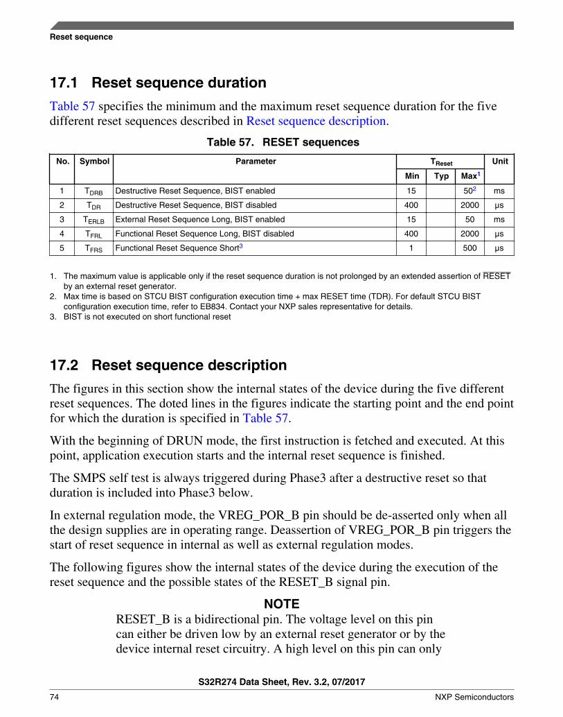
17.1 Reset sequence duration
Table 57 specifies the minimum and the maximum reset sequence duration for the fivedifferent reset sequences described in Reset sequence description.
Table 57. RESET sequences
No. Symbol Parameter TReset Unit
Min Typ Max1
1 TDRB Destructive Reset Sequence, BIST enabled 15 502 ms
2 TDR Destructive Reset Sequence, BIST disabled 400 2000 µs
3 TERLB External Reset Sequence Long, BIST enabled 15 50 ms
4 TFRL Functional Reset Sequence Long, BIST disabled 400 2000 µs
5 TFRS Functional Reset Sequence Short3 1 500 µs
1. The maximum value is applicable only if the reset sequence duration is not prolonged by an extended assertion of RESETby an external reset generator.
2. Max time is based on STCU BIST configuration execution time + max RESET time (TDR). For default STCU BISTconfiguration execution time, refer to EB834. Contact your NXP sales representative for details.
3. BIST is not executed on short functional reset
17.2 Reset sequence description
The figures in this section show the internal states of the device during the five differentreset sequences. The doted lines in the figures indicate the starting point and the end pointfor which the duration is specified in Table 57.
With the beginning of DRUN mode, the first instruction is fetched and executed. At thispoint, application execution starts and the internal reset sequence is finished.
The SMPS self test is always triggered during Phase3 after a destructive reset so thatduration is included into Phase3 below.
In external regulation mode, the VREG_POR_B pin should be de-asserted only when allthe design supplies are in operating range. Deassertion of VREG_POR_B pin triggers thestart of reset sequence in internal as well as external regulation modes.
The following figures show the internal states of the device during the execution of thereset sequence and the possible states of the RESET_B signal pin.
NOTERESET_B is a bidirectional pin. The voltage level on this pincan either be driven low by an external reset generator or by thedevice internal reset circuitry. A high level on this pin can only
Reset sequence
S32R274 Data Sheet, Rev. 3.2, 07/2017
74 NXP Semiconductors
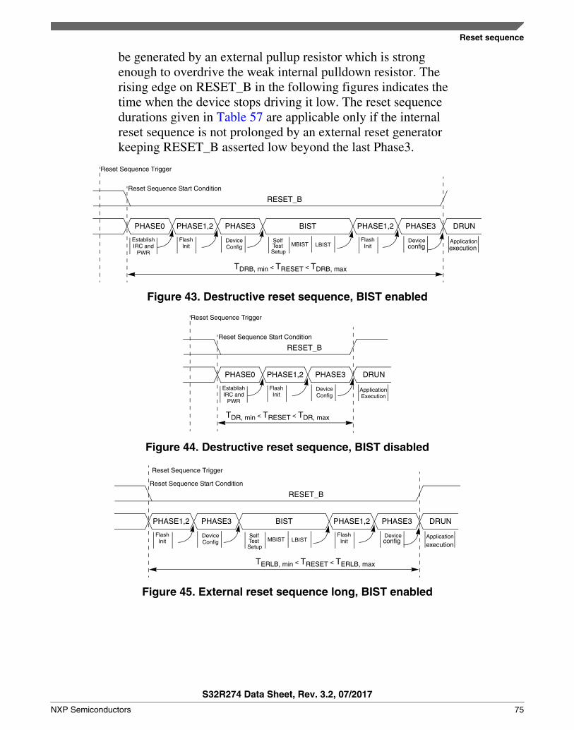
be generated by an external pullup resistor which is strongenough to overdrive the weak internal pulldown resistor. Therising edge on RESET_B in the following figures indicates thetime when the device stops driving it low. The reset sequencedurations given in Table 57 are applicable only if the internalreset sequence is not prolonged by an external reset generatorkeeping RESET_B asserted low beyond the last Phase3.
PHASE0 PHASE1,2 PHASE3 PHASE1,2 PHASE3 DRUNBIST
Reset Sequence Trigger
Reset Sequence Start Condition
RESET_B
Establish Flash Device Self MBIST LBIST Application
IRC and PWR
Init Test Setup Config
FlashInit Device
TDRB, min < TRESET < TDRB, max
executionconfig
Figure 43. Destructive reset sequence, BIST enabled
PHASE0 PHASE1,2 PHASE3 DRUN
Reset Sequence Trigger
Reset Sequence Start Condition
RESET_B
Establish Flash Device ApplicationIRC and
PWRInit Config Execution
TDR, min < TRESET < TDR, max
Figure 44. Destructive reset sequence, BIST disabled
PHASE1,2 PHASE3 PHASE1,2 PHASE3 DRUNBIST
Reset Sequence Trigger
Reset Sequence Start Condition
RESET_B
Flash Device Self MBIST LBIST Application
Init Test Setup Config
FlashInit Device
TERLB, min < TRESET < TERLB, max
executionconfig
Figure 45. External reset sequence long, BIST enabled
Reset sequence
S32R274 Data Sheet, Rev. 3.2, 07/2017
NXP Semiconductors 75
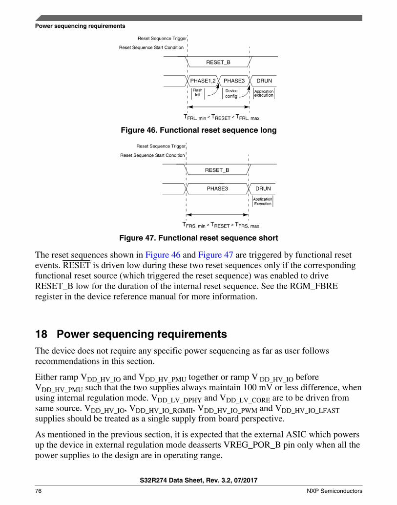
PHASE1, 2 PHASE3 DRUN
Reset Sequence Trigger
Reset Sequence Start Condition
RESET_B
ApplicationFlashInit Device
TFRL, min < TRESET < TFRL, max
executionconfig
Figure 46. Functional reset sequence long
PHASE3 DRUN
Reset Sequence Trigger
Reset Sequence Start Condition
RESET_B
ApplicationExecution
TFRS, min < TRESET < TFRS, max
Figure 47. Functional reset sequence short
The reset sequences shown in Figure 46 and Figure 47 are triggered by functional resetevents. RESET is driven low during these two reset sequences only if the correspondingfunctional reset source (which triggered the reset sequence) was enabled to driveRESET_B low for the duration of the internal reset sequence. See the RGM_FBREregister in the device reference manual for more information.
18 Power sequencing requirementsThe device does not require any specific power sequencing as far as user followsrecommendations in this section.
Either ramp VDD_HV_IO and VDD_HV_PMU together or ramp V DD_HV_IO beforeVDD_HV_PMU such that the two supplies always maintain 100 mV or less difference, whenusing internal regulation mode. VDD_LV_DPHY and VDD_LV_CORE are to be driven fromsame source. VDD_HV_IO, VDD_HV_IO_RGMII, VDD_HV_IO_PWM and VDD_HV_IO_LFASTsupplies should be treated as a single supply from board perspective.
As mentioned in the previous section, it is expected that the external ASIC which powersup the device in external regulation mode deasserts VREG_POR_B pin only when all thepower supplies to the design are in operating range.
Power sequencing requirements
S32R274 Data Sheet, Rev. 3.2, 07/2017
76 NXP Semiconductors

It should be noted that LVD and HVD detectors on VDD supply are disabled by defaultin external regulation mode for preventing a conflict with external regulator operation butthey can be enabled by software once design is powered up.
While designing the system, it is important to ensure that AFE supplies are powered upbefore data is sent on its input pads.
Pinouts
19.1 Package pinouts and signal descriptions
For package pinouts and signal descriptions, refer to the Reference Manual.
20 Revision HistoryTable 58. Revision History
Revision Date Description
1 8 Sep 2015 Initial release
2 25 Nov2016
• Editorial changes.• Replaced the term 'Freescale' with 'NXP' throughout the document.• In Family comparison table,
• 'MPC5775K' column, added FD support for MCAN• In Fields section, added detailed information about supported chip parts.• In Commercial product code structure figure, Tape and Reel indicator field, removed the 'T'
(Tray/Tubes) category.• In Absolute maximum ratings table,
• removed footnote 1 "Absolute maximum voltages ....been determined."• revised footnote for TVDD.
• In Operating conditions table,• 'TA' parameter maximum value updated from 105oC to 125oC, updated foonote
• From: When determining if the operating temperature specifications are met,either the ambient temperature or junction temperature specification can beused. It is not necessary that both specifications be met at all times. However,it is critical that the junction temperature specification is not exceeded underany condition.
• To: While determining if the operating temperature specifications are met,either the ambient temperature or junction temperature specification can beused. It is critical that the junction temperature specification is not exceededunder any condition.
• 'TA' parameter, updated footnote• From: Full performance means Core0 running @ 133.33 MHz, Core1/2
running @ 266.66 MHz, SPT running @ 200 MHz, rich set of peripherals used.• To: Full performance means Core0 running @ 120 MHz, Core1/2 running @
240 MHz, SPT running @ 200 MHz, rich set of peripherals used.• updated VDD_LV_DPHY typical value to 1.25 V and added a footnote to refer to
'AN5251'.• revised LVDSVinxoscclk(p-p) values.
Table continues on the next page...
19
Pinouts
S32R274 Data Sheet, Rev. 3.2, 07/2017
NXP Semiconductors 77

Table 58. Revision History
Revision Date Description
• updated units of RTRIM_TEMPCO as ppm/℃ and RTRIM_TOL as kΩ.
• in AFE Bypass Modes Only, Single-Ended External Clock section,• added 'Vinxoscjit' parameter• Vinxosclk parameter is split into two parameters as 'Vinxosccclkvil' and 'Vinxosccclkvih'• tdc is updated to 47(min), 50(typ), 53(max) %
• in AFE Bypass Modes Only, Differential-Ended External Clocks section,• added LVDSIinxoscclk - min 3.0 V and max 4.0 V• added LVDSVinxoscjit• added tdcLVDS is updated to 47 (min), 50 (typ), 53 (max) %
In Current consumption characteristics table,• updated IDD_CORE maximum value from 1752 mA to 1480 mA,• updated IDD_HV_FLA maximum value from 30 mA to 40 mA,• updated IDD_LV_DPHY typical value to 14.9 mA and maximum value to 23.2 mA.
• In Voltage regulator electrical specifications table, VREGSWPUP parameter, removedmin/typ/max values and added a footnote, "There is a strong pull up .... ground if unused."
• In RGMII pad DC electrical characteristics,• renamed 'Vih_hys' as 'Vih' and 'Vil_hys' as 'Vil'• added foonotes in 'Ioh_f' and 'Iol_f'
• In Functional Pad electrical characteristics table,• SIUL2_MSCR[SRC] '11'
• for 50 pF load, updated min to 0.7/0.6 ns and max to 3/3 ns• for 200pF load, updated min to 2.5/2.0 ns
• SIUL2_MSCR[SRC] '10'• for 25 pF load, updated min to 0.4/0.3 ns and max to 3.5/3.5 ns• for 50 pF load, updated min to 1.0/0.8 ns and max to 6.5/6.5 ns• for 200pF load, updated min to 6.5/3.0 ns
• In Aurora LVDS driver electrical characteristics table, updated FTXRX data rate as 1.15Gbps.
• In RESET_B electrical characteristics table,• updated IWPD parameter maximum spec from 80 uA to 100 uA.• IOL_R parameter, updated condition VDD_HV_IO from 1.0 V to 1.2 V.• removed IWPU parameter
• In 40 MHz Oscillator (XOSC) electrical characteristics table, revised VCMLVDS values andadded footnote in RinLVDS
• In Internal RC Oscillator electrical specifications table, updated footnote 1.• In 320 MHz AFE PLL parameters table, added tjitcc and 'Output duty cycle'.• In Sigma Delta ADC electrical characteristics,
• updated gain mismatch spec to -/+3.5 %• SNRSDA_MM_ON – min value updated to 63 dBFS and updated conditions column.• SNRSDA_MM_OFF– min value updated to 65 dBFS and updated conditions
column.• removed extraneous rows for SNRSDA_MM_ON and SNRSDA_MM_OFF• SNDRSDA_MM_ON and SNDRSDA_MM_OFF - updated conditions column and
removed removed extraneous rows for SNDRSDA_MM_ON andSNDRSDA_MM_OFF.
• IMDSDA_MM_ON - min value updated as 62 dBc and IMDSDA_MM_OFF - minvalue updated as 55 dBc.
• In DAC electrical specifications,• updated DNL minimum value from -18 LSB to -24 LSB.• updated PSRR min to 30 dB and added a footnote.
• In Flash memory program and erase specifications changed symbols for specifications:• Quad-page (1024 bits) program time: Changed symbol from tqppgn to tqppgm• 16 KB Block program time: Changed symbol from t16kpgn to t16kpgm
• In Flash memory AC timing specifications for tpsus:
Table continues on the next page...
Revision History
S32R274 Data Sheet, Rev. 3.2, 07/2017
78 NXP Semiconductors

Table 58. Revision History (continued)
Revision Date Description
• Changed Typical from 7 µs plus four system clock periods to 9.4 µs plus four systemclock periods
• Changed Max from 9.1 µs plus four system clock periods to 11.5 µs plus four systemclock periods
• In Ethernet switching specifications, added RMII timing diagrams, updated specs in the'Ethernet MDIO timing table'.
• In Serial Peripheral Interface (SPI) timing specifications,• updated tSDC specs• updated tDIS spec to 25 ns• updated tCSC min spec to 63.8 ns and tASC min spec to 68.8 ns• added footnotes in tPCSC and tPASC
• Added I2C timings section.• In External interrupt timing (IRQ pin) table, added a note, " tCYC is equivalent....for
details".• Revised Table 55.• Revised first paragraph in the General notes for specifications at maximum junction
temperature section.• In Reset sequence duration, added footnote 2 and 3 and updated description of TFRS.• In Power sequencing requirements section, removed the sentence, "Design may
experience 1 mA ....functional implication."
3 09 Mar2017
• In Table 7• updated LVDS external clock input voltage Max changed from 1.23V to 1.36V.
• In Power sequencing requirements• updated name from VDD_HV_PMC to VDD_HV_PMU.
3.1 06 Apr 2017 • Removed Preliminary from the footers.
3.2 17 July2017
• Removed Confidential Proprietary from the footers.
Revision History
S32R274 Data Sheet, Rev. 3.2, 07/2017
NXP Semiconductors 79

How to Reach Us:
Home Page:nxp.com
Web Support:nxp.com/support
Information in this document is provided solely to enable system and software
implementers to use NXP products. There are no express or implied copyright
licenses granted hereunder to design or fabricate any integrated circuits based
on the information in this document. NXP reserves the right to make changes
without further notice to any products herein.
NXP makes no warranty, representation, or guarantee regarding the suitability of
its products for any particular purpose, nor does NXP assume any liability arising
out of the application or use of any product or circuit, and specifically disclaims
any and all liability, including without limitation consequential or incidental
damages. “Typical” parameters that may be provided in NXP data sheets and/or
specifications can and do vary in different applications, and actual performance
may vary over time. All operating parameters, including “typicals,” must be
validated for each customer application by customerʼs technical experts. NXP
does not convey any license under its patent rights nor the rights of others. NXP
sells products pursuant to standard terms and conditions of sale, which can be
found at the following address: nxp.com/SalesTermsandConditions.
NXP, the NXP logo, NXP SECURE CONNECTIONS FOR A SMARTER
WORLD, COOLFLUX, EMBRACE, GREENCHIP, HITAG, I2C BUS, ICODE,
JCOP, LIFE VIBES, MIFARE, MIFARE CLASSIC, MIFARE DESFire, MIFARE
PLUS, MIFARE FLEX, MANTIS, MIFARE ULTRALIGHT, MIFARE4MOBILE,
MIGLO, NTAG, ROADLINK, SMARTLX, SMARTMX, STARPLUG, TOPFET,
TRENCHMOS, UCODE, Freescale, the Freescale logo, AltiVec, C-5, CodeTest,
CodeWarrior, ColdFire, ColdFire+, C-Ware, the Energy Efficient Solutions logo,
Kinetis, Layerscape, MagniV, mobileGT, PEG, PowerQUICC, Processor Expert,
QorIQ, QorIQ Qonverge, Ready Play, SafeAssure, the SafeAssure logo,
StarCore, Symphony, VortiQa, Vybrid, Airfast, BeeKit, BeeStack, CoreNet,
Flexis, MXC, Platform in a Package, QUICC Engine, SMARTMOS, Tower,
TurboLink, and UMEMS are trademarks of NXP B.V. All other product or service
names are the property of their respective owners. ARM, AMBA, ARM Powered,
Artisan, Cortex, Jazelle, Keil, SecurCore, Thumb, TrustZone, and μVision are
registered trademarks of ARM Limited (or its subsidiaries) in the EU and/or
elsewhere. ARM7, ARM9, ARM11, big.LITTLE, CoreLink, CoreSight,
DesignStart, Mali, mbed, NEON, POP, Sensinode, Socrates, ULINK and
Versatile are trademarks of ARM Limited (or its subsidiaries) in the EU and/or
elsewhere. All rights reserved. Oracle and Java are registered trademarks of
Oracle and/or its affiliates. The Power Architecture and Power.org word marks
and the Power and Power.org logos and related marks are trademarks and
service marks licensed by Power.org.
© 2015 NXP B.V.
Document Number S32R274Revision 3.2, 07/2017