s5-155u, cpu 948 - siemens...s5-155u cpu 948 programming guide this manual has the order number:...
TRANSCRIPT
Contents
Introduction 1
User Program 2
Program Execution 3
Operating Statuses and ProgramExecution Levels 4
Interrupt and Error Diagnostics 5
Integrated Special Functions 6
Extended Data Block DX 0 7Memory Assignment and MemoryOrganization 8Memory Access Using AbsoluteAddresses 9
Multiprocessor Mode and Com-munication in the S5-155U 10
PG Interfaces and Functions 11
Appendix 12Indexes:AbbreviationsKey Words 13The List of Operations, order no.6ES5 997-3UA22, is includedwith this manual.
10/98C79000-G8576-C848Release 04
S5-155UCPU 948
Programming Guide
This manual has the order number:6ES5 998–3PR21
SIMATIC S5
!Danger
indicates that death, severe personal injury or substantial property damage will result if proper precautions are nottaken.
!Warning
indicates that death, severe personal injury or substantial property damage can result if proper precautions are nottaken.
!Caution
indicates that minor personal injury or property damage can result if proper precautions are not taken.
Note
draws your attention to particularly important information on the product, handling the product, or to a particularpart of the documentation.
Qualified PersonnelThe device/system may only be set up and operated in conjunction with this manual.Only qualified personnel should be allowed to install and work on this equipment. Qualified persons are definedas persons who are authorized to commission, to ground, and to tag circuits, equipment, and systems in accor-dance with established safety practices and standards.
Correct UsageNote the following:
!Warning
This device and its components may only be used for the applications described in the catalog or the technicaldescription, and only in connection with devices or components from other manufacturers which have been ap-proved or recommended by Siemens.
This product can only function correctly and safely if it is transported, stored, set up, and installed correctly, andoperated and maintained as recommended.
TrademarksSIMATIC�, SIMATIC NET� and SIMATIC HMI� are registered trademarks of SIEMENS AG. Third parties usingfor their own purposes any other names in this document which refer to trademarks might infringe upon the rightsof the trademark owners.
We have checked the contents of this manual for agreement with thehardware and software described. Since deviations cannot beprecluded entirely, we cannot guarantee full agreement. However,the data in this manual are reviewed regularly and any necessarycorrections included in subsequent editions. Suggestions forimprovement are welcomed.
� Siemens AG 1998Subject to change without prior notice.
Disclaimer of LiabilityCopyright � Siemens AG 1998 All rights reserved
The reproduction, transmission or use of this document or itscontents is not permitted without express written authority.Offenders will be liable for damages. All rights, including rightscreated by patent grant or registration of a utility model or design, arereserved.
Siemens AGBereich Automatisierungs- und AntriebstechnikGeschaeftsgebiet Industrie-AutomatisierungssystemePostfach 4848, D-90327 Nuernberg
Siemens Aktiengesellschaft 6ES5 998-3PR21
Safety GuidelinesThis manual contains notices which you should observe to ensure your own personal safety, as well as to protectthe product and connected equipment. These notices are highlighted in the manual by a warning triangle and aremarked as follows according to the level of danger:
1 Introduction . . . . . . . . . . . . . . . . . . . . . . . . . . . . . . . . . . . . . . . . . . . . . . . . . . . . . . . . . . . . . . . . . 1 - 3
1.1 Area of Application for the S5-155U with the CPU 948 . . . . . . . . . . . . . . . . . . . . . . . . . . . . . . . 1 - 4
1.2 Typical Mode of Operation of a CPU . . . . . . . . . . . . . . . . . . . . . . . . . . . . . . . . . . . . . . . . . . . . . . 1 - 5
1.3 The Programs in a CPU . . . . . . . . . . . . . . . . . . . . . . . . . . . . . . . . . . . . . . . . . . . . . . . . . . . . . . . . . 1 - 7
1.4 Which Operands are available to the User Program?. . . . . . . . . . . . . . . . . . . . . . . . . . . . . . . . . 1 - 11
1.5 How much Memory is available for the User Program? . . . . . . . . . . . . . . . . . . . . . . . . . . . . . . 1 - 14
1.6 How to Tackle Programming. . . . . . . . . . . . . . . . . . . . . . . . . . . . . . . . . . . . . . . . . . . . . . . . . . . . 1 - 15
1.7 Programming Tools . . . . . . . . . . . . . . . . . . . . . . . . . . . . . . . . . . . . . . . . . . . . . . . . . . . . . . . . . . . 1 - 18
1.8 Converting User Programs of the CPU 928B for the CPU 948. . . . . . . . . . . . . . . . . . . . . . . . . 1 - 19
2 User Program . . . . . . . . . . . . . . . . . . . . . . . . . . . . . . . . . . . . . . . . . . . . . . . . . . . . . . . . . . . . . . . . 2 - 3
2.1 STEP 5 Programming Language . . . . . . . . . . . . . . . . . . . . . . . . . . . . . . . . . . . . . . . . . . . . . . . . . . 2 - 4
2.1.1 The LAD, CSF, STL Methods of Representation . . . . . . . . . . . . . . . . . . . . . . . . . . . . . . . . . . . . . 2 - 4
2.1.2 Structured Programming . . . . . . . . . . . . . . . . . . . . . . . . . . . . . . . . . . . . . . . . . . . . . . . . . . . . . . . . 2 - 5
2.1.3 STEP 5 Operations . . . . . . . . . . . . . . . . . . . . . . . . . . . . . . . . . . . . . . . . . . . . . . . . . . . . . . . . . . . . . 2 - 6
2.1.4 Number Representation . . . . . . . . . . . . . . . . . . . . . . . . . . . . . . . . . . . . . . . . . . . . . . . . . . . . . . . . . 2 - 8
2.1.5 STEP 5 Blocks and Storing them in Memory. . . . . . . . . . . . . . . . . . . . . . . . . . . . . . . . . . . . . . . 2 - 12
2.2 Program, Organization and Sequence Blocks . . . . . . . . . . . . . . . . . . . . . . . . . . . . . . . . . . . . . . . 2 - 16
2.2.1 Organization Blocks as User Interfaces . . . . . . . . . . . . . . . . . . . . . . . . . . . . . . . . . . . . . . . . . . . 2 - 18
2.2.2 Organization Blocks for Special Functions. . . . . . . . . . . . . . . . . . . . . . . . . . . . . . . . . . . . . . . . . 2 - 22
2.3 Function Blocks . . . . . . . . . . . . . . . . . . . . . . . . . . . . . . . . . . . . . . . . . . . . . . . . . . . . . . . . . . . . . . 2 - 23
2.3.1 Structure of Function Blocks . . . . . . . . . . . . . . . . . . . . . . . . . . . . . . . . . . . . . . . . . . . . . . . . . . . . 2 - 24
2.3.2 Programming Function Blocks . . . . . . . . . . . . . . . . . . . . . . . . . . . . . . . . . . . . . . . . . . . . . . . . . . 2 - 26
2.3.3 Calling Function Blocks and Assigning Parameters to them . . . . . . . . . . . . . . . . . . . . . . . . . . . 2 - 28
2.3.4 Special Function Blocks. . . . . . . . . . . . . . . . . . . . . . . . . . . . . . . . . . . . . . . . . . . . . . . . . . . . . . . . 2 - 33
2.4 Data Blocks . . . . . . . . . . . . . . . . . . . . . . . . . . . . . . . . . . . . . . . . . . . . . . . . . . . . . . . . . . . . . . . . . 2 - 35
2.4.1 Creating Data Blocks . . . . . . . . . . . . . . . . . . . . . . . . . . . . . . . . . . . . . . . . . . . . . . . . . . . . . . . . . . 2 - 37
2.4.2 Opening Data Blocks . . . . . . . . . . . . . . . . . . . . . . . . . . . . . . . . . . . . . . . . . . . . . . . . . . . . . . . . . . 2 - 38
2.4.3 Special Data Blocks . . . . . . . . . . . . . . . . . . . . . . . . . . . . . . . . . . . . . . . . . . . . . . . . . . . . . . . . . . . 2 - 41
Contents
CPU 948 Programming Guide
C79000-G8576-C848-04 iii
3 Program Execution. . . . . . . . . . . . . . . . . . . . . . . . . . . . . . . . . . . . . . . . . . . . . . . . . . . . . . . . . . . . 3 - 3
3.1 Principle of Program Execution. . . . . . . . . . . . . . . . . . . . . . . . . . . . . . . . . . . . . . . . . . . . . . . . . . . 3 - 4
3.2 Program Organization . . . . . . . . . . . . . . . . . . . . . . . . . . . . . . . . . . . . . . . . . . . . . . . . . . . . . . . . . . 3 - 5
3.3 Storing Program and Data Blocks . . . . . . . . . . . . . . . . . . . . . . . . . . . . . . . . . . . . . . . . . . . . . . . . 3 - 10
3.4 Processing the User Program. . . . . . . . . . . . . . . . . . . . . . . . . . . . . . . . . . . . . . . . . . . . . . . . . . . . 3 - 11
3.4.1 Definition of Terms used in Program Execution . . . . . . . . . . . . . . . . . . . . . . . . . . . . . . . . . . . . 3 - 12
3.5 STEP 5 Operations with Examples . . . . . . . . . . . . . . . . . . . . . . . . . . . . . . . . . . . . . . . . . . . . . . . 3 - 15
3.5.1 Basic Operations . . . . . . . . . . . . . . . . . . . . . . . . . . . . . . . . . . . . . . . . . . . . . . . . . . . . . . . . . . . . . 3 - 19
3.5.2 Programming Examples in the STL, LAD and CSF Methods of Representation. . . . . . . . . . . 3 - 34
3.5.3 Supplementary Operations . . . . . . . . . . . . . . . . . . . . . . . . . . . . . . . . . . . . . . . . . . . . . . . . . . . . . . 3 - 49
3.5.4 Executive Operations . . . . . . . . . . . . . . . . . . . . . . . . . . . . . . . . . . . . . . . . . . . . . . . . . . . . . . . . . . 3 - 59
3.5.5 Semaphore Operations . . . . . . . . . . . . . . . . . . . . . . . . . . . . . . . . . . . . . . . . . . . . . . . . . . . . . . . . . 3 - 75
4 Operating Statuses and Program Execution Levels . . . . . . . . . . . . . . . . . . . . . . . . . . . . . . . . 4 - 3
4.1 Program Execution Levels . . . . . . . . . . . . . . . . . . . . . . . . . . . . . . . . . . . . . . . . . . . . . . . . . . . . . . . 4 - 4
4.2 STOP Mode . . . . . . . . . . . . . . . . . . . . . . . . . . . . . . . . . . . . . . . . . . . . . . . . . . . . . . . . . . . . . . . . . . 4 - 9
4.2.1 SOFT STOP . . . . . . . . . . . . . . . . . . . . . . . . . . . . . . . . . . . . . . . . . . . . . . . . . . . . . . . . . . . . . . . . . . 4 - 9
4.2.2 HARD STOP . . . . . . . . . . . . . . . . . . . . . . . . . . . . . . . . . . . . . . . . . . . . . . . . . . . . . . . . . . . . . . . . 4 - 13
4.2.3 OVERALL RESET . . . . . . . . . . . . . . . . . . . . . . . . . . . . . . . . . . . . . . . . . . . . . . . . . . . . . . . . . . . 4 - 14
4.3 START-UP Mode . . . . . . . . . . . . . . . . . . . . . . . . . . . . . . . . . . . . . . . . . . . . . . . . . . . . . . . . . . . . . 4 - 16
4.3.1 MANUAL and AUTOMATIC COLD RESTART . . . . . . . . . . . . . . . . . . . . . . . . . . . . . . . . . . . 4 - 17
4.3.2 MANUAL and AUTOMATIC WARM RESTART. . . . . . . . . . . . . . . . . . . . . . . . . . . . . . . . . . . 4 - 18
4.3.3 Comparison between COLD RESTART and WARM RESTART . . . . . . . . . . . . . . . . . . . . . . . 4 - 21
4.3.4 RETENTIVE COLD RESTART . . . . . . . . . . . . . . . . . . . . . . . . . . . . . . . . . . . . . . . . . . . . . . . . . 4 - 22
4.3.5 Comparison of COLD RESTART and RETENTIVE COLD RESTART . . . . . . . . . . . . . . . . . 4 - 23
4.3.6 User Interfaces for Start-Up. . . . . . . . . . . . . . . . . . . . . . . . . . . . . . . . . . . . . . . . . . . . . . . . . . . . . 4 - 24
4.3.7 Extended AUTOMATIC WARM RESTART with the CPU 948 (HOT RESTART). . . . . . . . . 4 - 27
4.3.8 Interruptions during START-UP . . . . . . . . . . . . . . . . . . . . . . . . . . . . . . . . . . . . . . . . . . . . . . . . . 4 - 28
4.4 RUN Mode . . . . . . . . . . . . . . . . . . . . . . . . . . . . . . . . . . . . . . . . . . . . . . . . . . . . . . . . . . . . . . . . . . 4 - 29
4.4.1 Cyclic Program Execution . . . . . . . . . . . . . . . . . . . . . . . . . . . . . . . . . . . . . . . . . . . . . . . . . . . . . . 4 - 30
4.4.2 Specifying Time and Interrupt-Driven Program Execution . . . . . . . . . . . . . . . . . . . . . . . . . . . . 4 - 32
4.4.3 Time-Controlled Program Execution. . . . . . . . . . . . . . . . . . . . . . . . . . . . . . . . . . . . . . . . . . . . . . 4 - 33
4.4.4 Interrupt-Driven Program Execution . . . . . . . . . . . . . . . . . . . . . . . . . . . . . . . . . . . . . . . . . . . . . . 4 - 41
5 Interrupt and Error Diagnostics . . . . . . . . . . . . . . . . . . . . . . . . . . . . . . . . . . . . . . . . . . . . . . . . 5 - 3
5.1 Frequent Errors in the User Program . . . . . . . . . . . . . . . . . . . . . . . . . . . . . . . . . . . . . . . . . . . . . . 5 - 4
5.2 Error Information . . . . . . . . . . . . . . . . . . . . . . . . . . . . . . . . . . . . . . . . . . . . . . . . . . . . . . . . . . . . . . 5 - 5
5.3 Procedure for Error Analysis . . . . . . . . . . . . . . . . . . . . . . . . . . . . . . . . . . . . . . . . . . . . . . . . . . . . . 5 - 8
5.4 Control Bits and Interrupt Stack . . . . . . . . . . . . . . . . . . . . . . . . . . . . . . . . . . . . . . . . . . . . . . . . . . 5 - 9
5.4.1 Control Bits . . . . . . . . . . . . . . . . . . . . . . . . . . . . . . . . . . . . . . . . . . . . . . . . . . . . . . . . . . . . . . . . . 5 - 10
5.4.2 ISTACK Content . . . . . . . . . . . . . . . . . . . . . . . . . . . . . . . . . . . . . . . . . . . . . . . . . . . . . . . . . . . . . 5 - 14
5.4.3 Example of Error Diagnosis using the ISTACK. . . . . . . . . . . . . . . . . . . . . . . . . . . . . . . . . . . . . 5 - 19
Contents
CPU 948 Programming Guide
iv C79000-G8576-C848-04
5.5 Error Handling Using Organization Blocks . . . . . . . . . . . . . . . . . . . . . . . . . . . . . . . . . . . . . . . . 5 - 20
5.6 Causes of Error and Reactions of the CPU. . . . . . . . . . . . . . . . . . . . . . . . . . . . . . . . . . . . . . . . . 5 - 23
5.6.1 OB 19: Calling a Logic Block That Is Not Loaded (KB) . . . . . . . . . . . . . . . . . . . . . . . . . . . . . 5 - 24
5.6.2 OB 19: Calling a Data Block That Is Not Loaded (KDB) . . . . . . . . . . . . . . . . . . . . . . . . . . . . . 5 - 24
5.6.3 OB 23/24, OB 28/29:Timeout Error (QVZ) . . . . . . . . . . . . . . . . . . . . . . . . . . . . . . . . . . . . . . . . 5 - 25
5.6.4 OB 25: Addressing Error (ADF) . . . . . . . . . . . . . . . . . . . . . . . . . . . . . . . . . . . . . . . . . . . . . . . . 5 - 26
5.6.5 OB 26: Cycle Time Exceeded Error (ZYK) . . . . . . . . . . . . . . . . . . . . . . . . . . . . . . . . . . . . . . . . 5 - 27
5.6.6 OB 27: (Substitution Error SUF). . . . . . . . . . . . . . . . . . . . . . . . . . . . . . . . . . . . . . . . . . . . . . . . . 5 - 28
5.6.7 OB 30: Parity Error and Timeout Error in the User Memory (PARE) . . . . . . . . . . . . . . . . . . . 5 - 28
5.6.8 OB 32: Load and Transfer Error (TRAF) . . . . . . . . . . . . . . . . . . . . . . . . . . . . . . . . . . . . . . . . . . 5 - 29
5.6.9 OB 33: Collision of Timed Interrupts Error (WEFES/WEFEH) . . . . . . . . . . . . . . . . . . . . . . . . 5 - 30
5.6.10 OB 34: Error with G DB/GX DX (FEDBX) . . . . . . . . . . . . . . . . . . . . . . . . . . . . . . . . . . . . . . . 5 - 32
5.6.11 OB 35: Communication Errors . . . . . . . . . . . . . . . . . . . . . . . . . . . . . . . . . . . . . . . . . . . . . . . . . . 5 - 32
5.6.12 OB 36: Error in Self-test . . . . . . . . . . . . . . . . . . . . . . . . . . . . . . . . . . . . . . . . . . . . . . . . . . . . . . . 5 - 33
5.7 Self-Test . . . . . . . . . . . . . . . . . . . . . . . . . . . . . . . . . . . . . . . . . . . . . . . . . . . . . . . . . . . . . . . . . . . . 5 - 34
5.7.1 Overview . . . . . . . . . . . . . . . . . . . . . . . . . . . . . . . . . . . . . . . . . . . . . . . . . . . . . . . . . . . . . . . . . . . 5 - 34
5.7.2 Description of the Test Functions . . . . . . . . . . . . . . . . . . . . . . . . . . . . . . . . . . . . . . . . . . . . . . . . 5 - 35
5.7.3 Settings . . . . . . . . . . . . . . . . . . . . . . . . . . . . . . . . . . . . . . . . . . . . . . . . . . . . . . . . . . . . . . . . . . . . . 5 - 37
5.7.4 Error Handling . . . . . . . . . . . . . . . . . . . . . . . . . . . . . . . . . . . . . . . . . . . . . . . . . . . . . . . . . . . . . . . 5 - 38
6 Integrated Special Functions . . . . . . . . . . . . . . . . . . . . . . . . . . . . . . . . . . . . . . . . . . . . . . . . . . . 6 - 3
6.1 Introduction . . . . . . . . . . . . . . . . . . . . . . . . . . . . . . . . . . . . . . . . . . . . . . . . . . . . . . . . . . . . . . . . . . 6 - 4
6.2 OB 121: Set/Read System Time . . . . . . . . . . . . . . . . . . . . . . . . . . . . . . . . . . . . . . . . . . . . . . . . . . 6 - 8
6.3 OB 122: "Disable Interrupts" On/Off . . . . . . . . . . . . . . . . . . . . . . . . . . . . . . . . . . . . . . . . . . . . . 6 - 12
6.4 OB 124: Delete STEP 5 Blocks. . . . . . . . . . . . . . . . . . . . . . . . . . . . . . . . . . . . . . . . . . . . . . . . . . 6 - 14
6.5 OB 125: Generate STEP 5 Blocks. . . . . . . . . . . . . . . . . . . . . . . . . . . . . . . . . . . . . . . . . . . . . . . . 6 - 17
6.6 OB 126: Define, Transfer Process Images . . . . . . . . . . . . . . . . . . . . . . . . . . . . . . . . . . . . . . . . . 6 - 20
6.7 OB 129: Battery State . . . . . . . . . . . . . . . . . . . . . . . . . . . . . . . . . . . . . . . . . . . . . . . . . . . . . . . . . 6 - 25
6.8 OB 131: Delete ACCUs 1, 2, 3 and 4. . . . . . . . . . . . . . . . . . . . . . . . . . . . . . . . . . . . . . . . . . . . . 6 - 26
6.9 OB 132/133: Roll-Up ACCU/Roll-Down ACCU. . . . . . . . . . . . . . . . . . . . . . . . . . . . . . . . . . . . 6 - 27
6.10 OB 141: "Disable Single Cyclic Timed Interrupts" On/Off . . . . . . . . . . . . . . . . . . . . . . . . . . . . 6 - 29
6.11 OB 142: "Delay All Interrupts" On/Off . . . . . . . . . . . . . . . . . . . . . . . . . . . . . . . . . . . . . . . . . . . 6 - 32
6.12 OB 143: "Delay Single Cyclic Timed Interrupts" On/Off . . . . . . . . . . . . . . . . . . . . . . . . . . . . . 6 - 35
6.13 OB 150: Set/Read System Time . . . . . . . . . . . . . . . . . . . . . . . . . . . . . . . . . . . . . . . . . . . . . . . . . 6 - 38
6.14 OB 151: Set/Read Time for Clock-Controlled Interrupt . . . . . . . . . . . . . . . . . . . . . . . . . . . . . . 6 - 43
6.15 OB 153: Set/Read Time for Delayed Interrupt . . . . . . . . . . . . . . . . . . . . . . . . . . . . . . . . . . . . . . 6 - 50
6.16 OB 180: Variable Data Block Access . . . . . . . . . . . . . . . . . . . . . . . . . . . . . . . . . . . . . . . . . . . . . 6 - 53
6.17 OB 181: Test Data Blocks (DB/DX) . . . . . . . . . . . . . . . . . . . . . . . . . . . . . . . . . . . . . . . . . . . . . 6 - 57
6.18 OB 182: Copy Data Area. . . . . . . . . . . . . . . . . . . . . . . . . . . . . . . . . . . . . . . . . . . . . . . . . . . . . . . 6 - 59
6.19 OB 202 to 205: Multiprocessor Communication . . . . . . . . . . . . . . . . . . . . . . . . . . . . . . . . . . . . 6 - 62
Contents
CPU 948 Programming Guide
C79000-G8576-C848-04 v
6.20 OB 222: Restart Cycle Monitoring Time . . . . . . . . . . . . . . . . . . . . . . . . . . . . . . . . . . . . . . . . . . 6 - 63
6.21 OB 223: Compare Start-Up Modes . . . . . . . . . . . . . . . . . . . . . . . . . . . . . . . . . . . . . . . . . . . . . . . 6 - 64
6.22 OB 254/255: Copy/Duplicate Data Blocks . . . . . . . . . . . . . . . . . . . . . . . . . . . . . . . . . . . . . . . . . 6 - 65
7 Extended Data Block DX 0 . . . . . . . . . . . . . . . . . . . . . . . . . . . . . . . . . . . . . . . . . . . . . . . . . . . . . 7 - 3
7.1 Application . . . . . . . . . . . . . . . . . . . . . . . . . . . . . . . . . . . . . . . . . . . . . . . . . . . . . . . . . . . . . . . . . . . 7 - 4
7.2 Structure of DX 0. . . . . . . . . . . . . . . . . . . . . . . . . . . . . . . . . . . . . . . . . . . . . . . . . . . . . . . . . . . . . . 7 - 5
7.2.1 Example of Input in DX 0 . . . . . . . . . . . . . . . . . . . . . . . . . . . . . . . . . . . . . . . . . . . . . . . . . . . . . . . 7 - 7
7.3 Parameters for DX 0 . . . . . . . . . . . . . . . . . . . . . . . . . . . . . . . . . . . . . . . . . . . . . . . . . . . . . . . . . . . 7 - 8
7.4 Examples of Parameter Assignment . . . . . . . . . . . . . . . . . . . . . . . . . . . . . . . . . . . . . . . . . . . . . . 7 - 12
7.4.1 STEP 5 Programming . . . . . . . . . . . . . . . . . . . . . . . . . . . . . . . . . . . . . . . . . . . . . . . . . . . . . . . . . 7 - 12
7.4.2 Parameter Assignment using the PG Screen Form . . . . . . . . . . . . . . . . . . . . . . . . . . . . . . . . . . . 7 - 14
8 Memory Assignment and Memory Organization. . . . . . . . . . . . . . . . . . . . . . . . . . . . . . . . . . . 8 - 3
8.1 Structure of the Memory Area. . . . . . . . . . . . . . . . . . . . . . . . . . . . . . . . . . . . . . . . . . . . . . . . . . . . 8 - 4
8.2 Memory Assignment in the CPU 948 . . . . . . . . . . . . . . . . . . . . . . . . . . . . . . . . . . . . . . . . . . . . . . 8 - 5
8.2.1 Memory Assignment for the System RAM . . . . . . . . . . . . . . . . . . . . . . . . . . . . . . . . . . . . . . . . 8 - 6
8.2.2 Memory Assignment for the Peripherals . . . . . . . . . . . . . . . . . . . . . . . . . . . . . . . . . . . . . . . . . 8 - 8
8.3 User Memory Organization in the CPU 948. . . . . . . . . . . . . . . . . . . . . . . . . . . . . . . . . . . . . . . . 8 - 10
8.3.1 Block Headers in User Memory . . . . . . . . . . . . . . . . . . . . . . . . . . . . . . . . . . . . . . . . . . . . . . . . . 8 - 12
8.3.2 Block Address List in Data Block DB 0. . . . . . . . . . . . . . . . . . . . . . . . . . . . . . . . . . . . . . . . . . . 8 - 13
8.3.3 RI/RJ Area . . . . . . . . . . . . . . . . . . . . . . . . . . . . . . . . . . . . . . . . . . . . . . . . . . . . . . . . . . . . . . . . . . 8 - 14
8.3.4 RS/RT Area. . . . . . . . . . . . . . . . . . . . . . . . . . . . . . . . . . . . . . . . . . . . . . . . . . . . . . . . . . . . . . . . . . 8 - 15
8.3.5 Bit Assignment of the System Data Words . . . . . . . . . . . . . . . . . . . . . . . . . . . . . . . . . . . . . . . . . 8 - 18
8.3.6 Addressable System Data Area . . . . . . . . . . . . . . . . . . . . . . . . . . . . . . . . . . . . . . . . . . . . . . . . . . 8 - 42
9 Memory Access Using Absolute Addresses . . . . . . . . . . . . . . . . . . . . . . . . . . . . . . . . . . . . . . . . 9 - 3
9.1 Introduction . . . . . . . . . . . . . . . . . . . . . . . . . . . . . . . . . . . . . . . . . . . . . . . . . . . . . . . . . . . . . . . . . . 9 - 4
9.2 Memory Access via Address in ACCU 1 . . . . . . . . . . . . . . . . . . . . . . . . . . . . . . . . . . . . . . . . . . . 9 - 8
9.2.1 LIR/TIR: Loading to or Transferring from a 16-Bit Memory Area Indirectly . . . . . . . . . . . . . . 9 - 9
9.2.2 Examples of Access to DW > 255 . . . . . . . . . . . . . . . . . . . . . . . . . . . . . . . . . . . . . . . . . . . . . . . 9 - 15
9.2.3 LDI/TDI: Loading to or Transferring from a 32-Bit Memory Area Indirectly . . . . . . . . . . . . . 9 - 17
9.3 Transferring Memory Blocks. . . . . . . . . . . . . . . . . . . . . . . . . . . . . . . . . . . . . . . . . . . . . . . . . . . . 9 - 19
9.4 Operations with the Base Address Register (BR Register) . . . . . . . . . . . . . . . . . . . . . . . . . . . . 9 - 22
9.4.1 Operations for Transfer between Registers . . . . . . . . . . . . . . . . . . . . . . . . . . . . . . . . . . . . . . . . . 9 - 23
9.4.2 Accessing the Local Memory . . . . . . . . . . . . . . . . . . . . . . . . . . . . . . . . . . . . . . . . . . . . . . . . . . . 9 - 24
9.4.3 Accessing the Global Memory . . . . . . . . . . . . . . . . . . . . . . . . . . . . . . . . . . . . . . . . . . . . . . . . . . 9 - 25
9.4.4 Accessing the Dual-Port RAM Memory . . . . . . . . . . . . . . . . . . . . . . . . . . . . . . . . . . . . . . . . . . 9 - 29
10 Multiprocessor Mode and Communication in the S5-155U . . . . . . . . . . . . . . . . . . . . . . . . . 10 - 3
10.1 Multiprocessor Mode . . . . . . . . . . . . . . . . . . . . . . . . . . . . . . . . . . . . . . . . . . . . . . . . . . . . . . . . . . 10 - 4
10.1.1 When to use the Multiprocessor Mode . . . . . . . . . . . . . . . . . . . . . . . . . . . . . . . . . . . . . . . . . . . . 10 - 4
10.1.2 What Communications Mechanisms are Available?. . . . . . . . . . . . . . . . . . . . . . . . . . . . . . . . . . 10 - 4
Contents
CPU 948 Programming Guide
vi C79000-G8576-C848-04
10.1.3 Exchanging Data via IPC Flags. . . . . . . . . . . . . . . . . . . . . . . . . . . . . . . . . . . . . . . . . . . . . . . . . . 10 - 5
10.1.4 Exchanging Data via Handling Blocks . . . . . . . . . . . . . . . . . . . . . . . . . . . . . . . . . . . . . . . . . . . . 10 - 8
10.1.5 What needs to be Programmed for the Multiprocessor Mode? . . . . . . . . . . . . . . . . . . . . . . . . . 10 - 9
10.1.6 How to Create Data Block DB 1. . . . . . . . . . . . . . . . . . . . . . . . . . . . . . . . . . . . . . . . . . . . . . . . . 10 - 9
10.1.7 Starting up in the Multiprocessor Mode . . . . . . . . . . . . . . . . . . . . . . . . . . . . . . . . . . . . . . . . . . 10 - 13
10.1.8 Test Mode. . . . . . . . . . . . . . . . . . . . . . . . . . . . . . . . . . . . . . . . . . . . . . . . . . . . . . . . . . . . . . . . . . 10 - 14
10.2 Multiprocessor Communication. . . . . . . . . . . . . . . . . . . . . . . . . . . . . . . . . . . . . . . . . . . . . . . . . 10 - 15
10.2.1 Introduction . . . . . . . . . . . . . . . . . . . . . . . . . . . . . . . . . . . . . . . . . . . . . . . . . . . . . . . . . . . . . . . . 10 - 15
10.2.2 How the Transmitter and Receiver are Identified . . . . . . . . . . . . . . . . . . . . . . . . . . . . . . . . . . 10 - 16
10.2.3 Why Data is Buffered . . . . . . . . . . . . . . . . . . . . . . . . . . . . . . . . . . . . . . . . . . . . . . . . . . . . . . . . 10 - 17
10.2.4 How the Buffer is Processed and Managed . . . . . . . . . . . . . . . . . . . . . . . . . . . . . . . . . . . . . . . 10 - 18
10.2.5 System Start-Up . . . . . . . . . . . . . . . . . . . . . . . . . . . . . . . . . . . . . . . . . . . . . . . . . . . . . . . . . . . . . 10 - 21
10.2.6 Calling Communication OBs. . . . . . . . . . . . . . . . . . . . . . . . . . . . . . . . . . . . . . . . . . . . . . . . . . . 10 - 22
10.2.7 How to Assign Parameters to Communication OBs. . . . . . . . . . . . . . . . . . . . . . . . . . . . . . . . . 10 - 23
10.2.8 How to Evaluate the Output Parameters . . . . . . . . . . . . . . . . . . . . . . . . . . . . . . . . . . . . . . . . . . 10 - 24
10.3 Runtimes of the Communication OBs. . . . . . . . . . . . . . . . . . . . . . . . . . . . . . . . . . . . . . . . . . . . 10 - 31
10.4 INITIALIZE Function (OB 200). . . . . . . . . . . . . . . . . . . . . . . . . . . . . . . . . . . . . . . . . . . . . . . . 10 - 33
10.4.1 Function . . . . . . . . . . . . . . . . . . . . . . . . . . . . . . . . . . . . . . . . . . . . . . . . . . . . . . . . . . . . . . . . . . . 10 - 33
10.4.2 Call Parameters. . . . . . . . . . . . . . . . . . . . . . . . . . . . . . . . . . . . . . . . . . . . . . . . . . . . . . . . . . . . . . 10 - 35
10.4.3 Input Parameters. . . . . . . . . . . . . . . . . . . . . . . . . . . . . . . . . . . . . . . . . . . . . . . . . . . . . . . . . . . . . 10 - 35
10.4.4 Output Parameters . . . . . . . . . . . . . . . . . . . . . . . . . . . . . . . . . . . . . . . . . . . . . . . . . . . . . . . . . . . 10 - 38
10.5 SEND Function (OB 202) . . . . . . . . . . . . . . . . . . . . . . . . . . . . . . . . . . . . . . . . . . . . . . . . . . . . . 10 - 40
10.5.1 Function . . . . . . . . . . . . . . . . . . . . . . . . . . . . . . . . . . . . . . . . . . . . . . . . . . . . . . . . . . . . . . . . . . . 10 - 40
10.5.2 Call Parameters. . . . . . . . . . . . . . . . . . . . . . . . . . . . . . . . . . . . . . . . . . . . . . . . . . . . . . . . . . . . . . 10 - 40
10.5.3 Input Parameters. . . . . . . . . . . . . . . . . . . . . . . . . . . . . . . . . . . . . . . . . . . . . . . . . . . . . . . . . . . . . 10 - 40
10.5.4 Output Parameters . . . . . . . . . . . . . . . . . . . . . . . . . . . . . . . . . . . . . . . . . . . . . . . . . . . . . . . . . . . 10 - 42
10.6 SEND TEST Function (OB 203) . . . . . . . . . . . . . . . . . . . . . . . . . . . . . . . . . . . . . . . . . . . . . . . 10 - 45
10.6.1 Function . . . . . . . . . . . . . . . . . . . . . . . . . . . . . . . . . . . . . . . . . . . . . . . . . . . . . . . . . . . . . . . . . . . 10 - 45
10.6.2 Call Parameters. . . . . . . . . . . . . . . . . . . . . . . . . . . . . . . . . . . . . . . . . . . . . . . . . . . . . . . . . . . . . . 10 - 45
10.6.3 Input Parameters. . . . . . . . . . . . . . . . . . . . . . . . . . . . . . . . . . . . . . . . . . . . . . . . . . . . . . . . . . . . . 10 - 45
10.6.4 Output Parameters . . . . . . . . . . . . . . . . . . . . . . . . . . . . . . . . . . . . . . . . . . . . . . . . . . . . . . . . . . . 10 - 45
10.7 RECEIVE Function (OB 204). . . . . . . . . . . . . . . . . . . . . . . . . . . . . . . . . . . . . . . . . . . . . . . . . . 10 - 47
10.7.1 Function . . . . . . . . . . . . . . . . . . . . . . . . . . . . . . . . . . . . . . . . . . . . . . . . . . . . . . . . . . . . . . . . . . . 10 - 47
10.7.2 Call Parameters. . . . . . . . . . . . . . . . . . . . . . . . . . . . . . . . . . . . . . . . . . . . . . . . . . . . . . . . . . . . . . 10 - 47
10.7.3 Input Parameters. . . . . . . . . . . . . . . . . . . . . . . . . . . . . . . . . . . . . . . . . . . . . . . . . . . . . . . . . . . . . 10 - 47
10.7.4 Output Parameters . . . . . . . . . . . . . . . . . . . . . . . . . . . . . . . . . . . . . . . . . . . . . . . . . . . . . . . . . . . 10 - 48
10.8 RECEIVE TEST Function (OB 205) . . . . . . . . . . . . . . . . . . . . . . . . . . . . . . . . . . . . . . . . . . . . 10 - 51
10.8.1 Function . . . . . . . . . . . . . . . . . . . . . . . . . . . . . . . . . . . . . . . . . . . . . . . . . . . . . . . . . . . . . . . . . . . 10 - 51
10.8.2 Call Parameters. . . . . . . . . . . . . . . . . . . . . . . . . . . . . . . . . . . . . . . . . . . . . . . . . . . . . . . . . . . . . . 10 - 51
10.8.3 Input Parameters. . . . . . . . . . . . . . . . . . . . . . . . . . . . . . . . . . . . . . . . . . . . . . . . . . . . . . . . . . . . . 10 - 51
10.8.4 Output Parameters . . . . . . . . . . . . . . . . . . . . . . . . . . . . . . . . . . . . . . . . . . . . . . . . . . . . . . . . . . . 10 - 51
Contents
CPU 948 Programming Guide
C79000-G8576-C848-04 vii
10.9 Applications . . . . . . . . . . . . . . . . . . . . . . . . . . . . . . . . . . . . . . . . . . . . . . . . . . . . . . . . . . . . . . . . 10 - 53
10.9.1 Calling the Special Function OB using Function Blocks . . . . . . . . . . . . . . . . . . . . . . . . . . . . . 10 - 53
10.9.2 Transferring Data Blocks . . . . . . . . . . . . . . . . . . . . . . . . . . . . . . . . . . . . . . . . . . . . . . . . . . . . . . 10 - 60
10.9.3 Extending the IPC Flag Area . . . . . . . . . . . . . . . . . . . . . . . . . . . . . . . . . . . . . . . . . . . . . . . . . . . 10 - 66
11 PG Interfaces and Functions . . . . . . . . . . . . . . . . . . . . . . . . . . . . . . . . . . . . . . . . . . . . . . . . . . 11 - 3
11.1 Overview . . . . . . . . . . . . . . . . . . . . . . . . . . . . . . . . . . . . . . . . . . . . . . . . . . . . . . . . . . . . . . . . . . . 11 - 4
11.2 PG Functions . . . . . . . . . . . . . . . . . . . . . . . . . . . . . . . . . . . . . . . . . . . . . . . . . . . . . . . . . . . . . . . . 11 - 5
11.2.1 Info 11 - 6
11.2.2 Installation . . . . . . . . . . . . . . . . . . . . . . . . . . . . . . . . . . . . . . . . . . . . . . . . . . . . . . . . . . . . . . . . . . 11 - 7
11.2.3 Program Test. . . . . . . . . . . . . . . . . . . . . . . . . . . . . . . . . . . . . . . . . . . . . . . . . . . . . . . . . . . . . . . . . 11 - 8
11.3 Serial Link PG - PLC via 1st or 2nd Serial Interface. . . . . . . . . . . . . . . . . . . . . . . . . . . . . . . . 11 - 16
11.4 Parallel Operation of Two Serial PG Interfaces . . . . . . . . . . . . . . . . . . . . . . . . . . . . . . . . . . . . 11 - 17
11.4.1 Installation . . . . . . . . . . . . . . . . . . . . . . . . . . . . . . . . . . . . . . . . . . . . . . . . . . . . . . . . . . . . . . . . . 11 - 19
11.4.2 Operation . . . . . . . . . . . . . . . . . . . . . . . . . . . . . . . . . . . . . . . . . . . . . . . . . . . . . . . . . . . . . . . . . . 11 - 19
11.4.3 Sequence in Certain Operating Situations. . . . . . . . . . . . . . . . . . . . . . . . . . . . . . . . . . . . . . . . . 11 - 21
11.5 PG Functions via the S5 Bus. . . . . . . . . . . . . . . . . . . . . . . . . . . . . . . . . . . . . . . . . . . . . . . . . . . 11 - 27
11.5.1 Application . . . . . . . . . . . . . . . . . . . . . . . . . . . . . . . . . . . . . . . . . . . . . . . . . . . . . . . . . . . . . . . . . 11 - 27
11.5.2 How the PG Functions Work via the S5 Bus . . . . . . . . . . . . . . . . . . . . . . . . . . . . . . . . . . . . . . 11 - 29
11.5.3 Installation and Getting Started . . . . . . . . . . . . . . . . . . . . . . . . . . . . . . . . . . . . . . . . . . . . . . . . . 11 - 31
11.5.4 Condition Codes Indicating Problems. . . . . . . . . . . . . . . . . . . . . . . . . . . . . . . . . . . . . . . . . . . . 11 - 35
12 Appendix . . . . . . . . . . . . . . . . . . . . . . . . . . . . . . . . . . . . . . . . . . . . . . . . . . . . . . . . . . . . . . . . . . . 12 - 3
13 Indexes . . . . . . . . . . . . . . . . . . . . . . . . . . . . . . . . . . . . . . . . . . . . . . . . . . . . . . . . . . . . . . . . . . . . . 13 - 3
Contents
CPU 948 Programming Guide
viii C79000-G8576-C848-04
Contents of Chapter 1
1.1 Area of Application for the S5-155U with the CPU 948 . . . . . . . . . . . . . . . . . . . . . . . . 1 - 4
1.2 Typical Mode of Operation of a CPU . . . . . . . . . . . . . . . . . . . . . . . . . . . . . . . . . . . . . . . 1 - 5
1.3 The Programs in a CPU . . . . . . . . . . . . . . . . . . . . . . . . . . . . . . . . . . . . . . . . . . . . . . . . . . 1 - 7
1.4 Which Operands are available to the User Program? . . . . . . . . . . . . . . . . . . . . . . . . . . 1 - 11
1.5 How much Memory is available for the User Program? . . . . . . . . . . . . . . . . . . . . . . . 1 - 14
1.6 How to Tackle Programming? . . . . . . . . . . . . . . . . . . . . . . . . . . . . . . . . . . . . . . . . . . . . 1 - 15
1.7 Programming Tools. . . . . . . . . . . . . . . . . . . . . . . . . . . . . . . . . . . . . . . . . . . . . . . . . . . . . 1 - 18
1.8 Converting User Programs of the CPU 928B for the CPU 948. . . . . . . . . . . . . . . . . . 1 - 19
1Introduction
CPU 948 Programming Guide
C79000-G8576-C848-04 1 - 1

Contents
CPU 948 Programming Guide
1 - 2 C79000-G8576-C848-04
1Introduction
Aims of the manual This manual is intended to provide specialized information aboutprogramming the CPU 948 for users who already have basicknowledge of programming PLCs and want to use the CPU 948 in theS5-155U programmable controller. If you do not yet have this basicknowledge, we strongly advise you read the documentationintroducing the programming language STEP 5 /3/ or take part in acourse at our training center. SIEMENS provides comprehensivetraining for SIMATIC S5. For more detailed information, contact yourlocal SIEMENS office.
Contents of Chapter 1 Chapter 1 explains how to use the manual and deals with the areas ofapplication of the S5-155U programmable controller with theCPU 948 and its structure.The chapter explains the typical mode of operation of a CPU and thestructure of the CPU program.You will also find a few suggestions about how to tackleprogramming and will learn some of the features of the CPU 948which are important for programming.If you have already worked with the CPU 946/947 and would like toknow the differences between these modules and the CPU 948, referto Section 1.8.
Chapter 1 also informs you about differences between versions A01and A02 of the CPU 948 and explains points you should rememberwhen converting "928B" programs for the CPU 948.
CPU 948 Programming Guide
C79000-G8576-C848-04 1 - 3

1.1 Area of Application for the S5-155U with the CPU 948
SIMATIC S5 family The S5-155U programmable controller belongs to the family ofSIMATIC S5 programmable controllers. With the CPU 948, it is themost powerful multiprocessor unit for process automation (open andclosed loop control, signalling, monitoring, logging).Owing to its modularity and high performance, it can be used formedium to extremely large control systems as well as for complexautomation tasks at the plant and process supervision level.
Suitability The S5-155U with the CPU 948 is particularly suitable for thefollowing:
•• Tasks requiring fast bit and word-oriented processing and fastreaction times, i.e. with extremely fast open and closed loop controls.Examples of this are fast processes in mechanical engineering(bottling plant, packing machines or similar systems) and in theautomobile industry.
•• Tasks requiring an extremely high storage capacity and fast accesstimes, e.g. in the automobile industry, process and plantengineering.
•• Tasks requiring fast communication with other CPUs installed inthe PLC and operating in the multiprocessor mode and with CPmodules (e.g. when connected to bus systems, host computers, forvisualization, operation and monitoring).
•• Complex tasks which can be handled efficiently and clearly usingthe high level languages C and SCL.
Area of Application for the S5-155U with the CPU 948
CPU 948 Programming Guide
1 - 4 C79000-G8576-C848-04
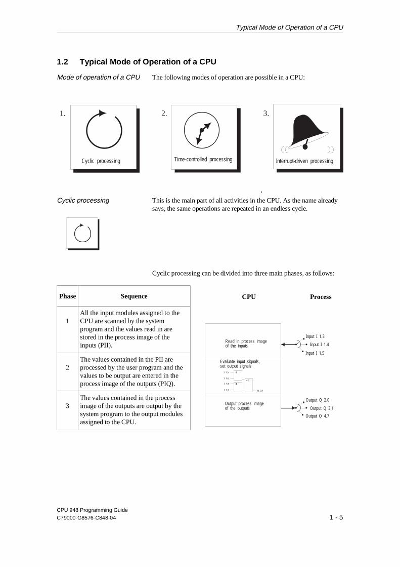
1.2 Typical Mode of Operation of a CPU
Mode of operation of a CPU The following modes of operation are possible in a CPU:
Cyclic processing This is the main part of all activities in the CPU. As the name alreadysays, the same operations are repeated in an endless cycle.
Cyclic processing can be divided into three main phases, as follows:
Phase Sequence
1All the input modules assigned to theCPU are scanned by the systemprogram and the values read in arestored in the process image of theinputs (PII).
2The values contained in the PII areprocessed by the user program and thevalues to be output are entered in theprocess image of the outputs (PIQ).
3The values contained in the processimage of the outputs are output by thesystem program to the output modulesassigned to the CPU.
Cyclic processing Interrupt-driven processingTime-controlled processing
1. 2. 3.
Read in process imageof the inputs
Output process imageof the outputs
&
&
= 1
I 1.5
I 1.6
I 1.4
I 1.3 Q 3.1
Evaluate input signals,set output signals
Input I 1.3
Input I 1.4
Input I 1.5
Output Q 3.1
Output Q 2.0
Output Q 4.7
CPU Process
Typical Mode of Operation of a CPU
CPU 948 Programming Guide
C79000-G8576-C848-04 1 - 5

Time-controlled processing In addition to the cyclic processing, time-controlled processing isalso available for processes requiring control signals at constantintervals, e.g. non-time critical monitoring functions performed everysecond.
Interrupt-driven processing If the reaction to a particular process signal must be particularly fast, thisshould be handled with interrupt-driven processing. With, for example,a system interrupt, triggered via an interrupt generating module, youcan activate a special processing section within your program.
Processing according topriority
The types of processing listed above are handled by the CPUaccording to their priority .
Since a fast reaction is required to a time or interrupt event, the CPUinterrupts cyclic processing to handle a time or interrupt event. Cyclicprocessing therefore has the lowest priority.
Whether or not the time-controlled processing is more important thanthe interrupt controlled processing depends, among other things, onthe particular task. For this reason, the priority of time andinterrupt-driven processing on the CPU 948 can be selected.
Typical Mode of Operation of a CPU
CPU 948 Programming Guide
1 - 6 C79000-G8576-C848-04
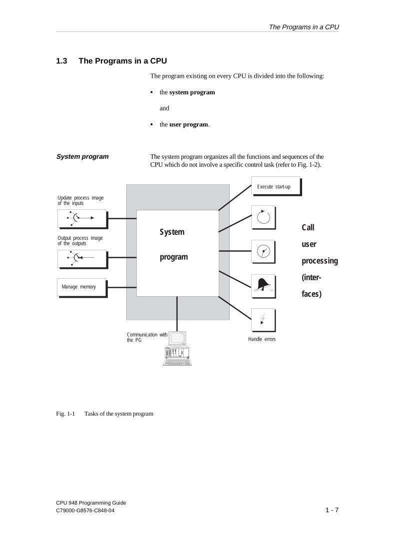
1.3 The Programs in a CPU
The program existing on every CPU is divided into the following:
•• the system program
and
•• the user program.
System program The system program organizes all the functions and sequences of theCPU which do not involve a specific control task (refer to Fig. 1-2).
Update process imageof the inputs
Output process imageof the outputs
System
program
Call
user
processing
(inter-
faces)
Execute start-up
Handle errorsCommunication withthe PG
Manage memory
Fig. 1-1 Tasks of the system program
The Programs in a CPU
CPU 948 Programming Guide
C79000-G8576-C848-04 1 - 7
Tasks The tasks include the following: 1)
•• cold and warm restart,
•• updating the process image of the inputs and outputting theprocess image of the outputs,
•• calling the cyclic, time-controlled and interrupt-driven programs,
•• detection and handling of errors,
•• memory management,
•• communication with the programmer (PG).
User interfaces As the user, you can influence the reaction of the CPU to particularsituations and errors via special interfaces to the system program.
Storing the system program After switching on the power supply to the PLC (POWER UP) thesystem program is read from the EPROM to the internal operatingsystem RAM.
System program defaults The following chapters, except for Chapter 7, describe the defaultsystem reaction to process events or errors. Depending on thedefaults, the CPU changes to the stop mode if an operation code erroroccurs and the error organization block is not loaded.
Modifying the defaults You can modify the system response by assigning parameters for thedata block DX 0.Chapter 7 describes the system response following modification.
1) When operating with several CPUs (multiprocessing) further tasks are involved.
The Programs in a CPU
CPU 948 Programming Guide
1 - 8 C79000-G8576-C848-04
User program
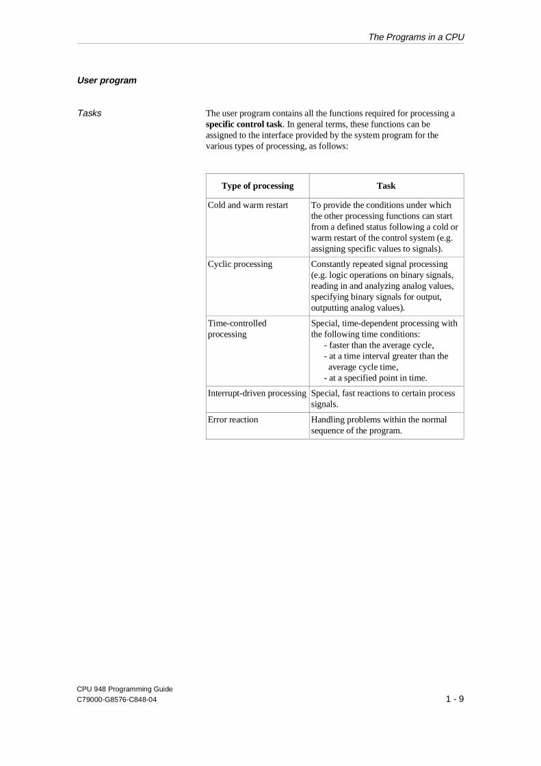
Tasks The user program contains all the functions required for processing aspecific control task. In general terms, these functions can beassigned to the interface provided by the system program for thevarious types of processing, as follows:
Type of processing Task
Cold and warm restart To provide the conditions under whichthe other processing functions can startfrom a defined status following a cold orwarm restart of the control system (e.g.assigning specific values to signals).
Cyclic processing Constantly repeated signal processing(e.g. logic operations on binary signals,reading in and analyzing analog values,specifying binary signals for output,outputting analog values).
Time-controlledprocessing
Special, time-dependent processing withthe following time conditions:
- faster than the average cycle,- at a time interval greater than the average cycle time,- at a specified point in time.
Interrupt-driven processing Special, fast reactions to certain processsignals.
Error reaction Handling problems within the normalsequence of the program.
The Programs in a CPU
CPU 948 Programming Guide
C79000-G8576-C848-04 1 - 9
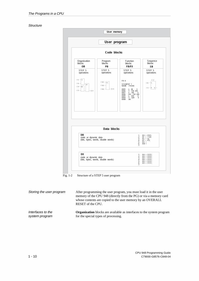
Structure
Storing the user program After programming the user program, you must load it in the usermemory of the CPU 948 (directly from the PG) or via a memory cardwhose contents are copied to the user memory by an OVERALLRESET of the CPU.
Interfaces to the system program
Organization blocks are available as interfaces to the system programfor the special types of processing.
User memory
Code blocks
Data blocks
Organizationblocks
OB
DB
DX
PB FB/FX SB
FB 8
SEGMENT 1NAME :TRANS
0005 :L IB 30006 :T FW 2000007 :C DB 50008 :DO FW 2000009 :L DW 0000A :T QW 6000B :BE
1: KH = 0101;2: KF = +120;3: KS = xy;4: KY = 4.5;5: KG =6: KM =7:
1: KH = FFFF;2: KH = FFFF;3: KH = FFFF;4: KH = FFFF;5: KH = FFFF;6: KH = FFFF;7:
STEP 5operations
static or dynamic data(bits, bytes, words, double words)
static or dynamic data(bits, bytes, words, double words)
STEP 5operations
STEP 5operations
STEP 5operations
Programblocks
Functionblocks
Sequenceblocks
&
&
= 1
I 1.5
I 1.6
I 1.4
I 1.3 Q 3.1
= 1F 50.1
F 50.2
F 50.3 Q 5.3
F 1.7
I 2.6 S
R QI 1.3
User program
Fig. 1-2 Structure of a STEP 5 user program
The Programs in a CPU
CPU 948 Programming Guide
1 - 10 C79000-G8576-C848-04
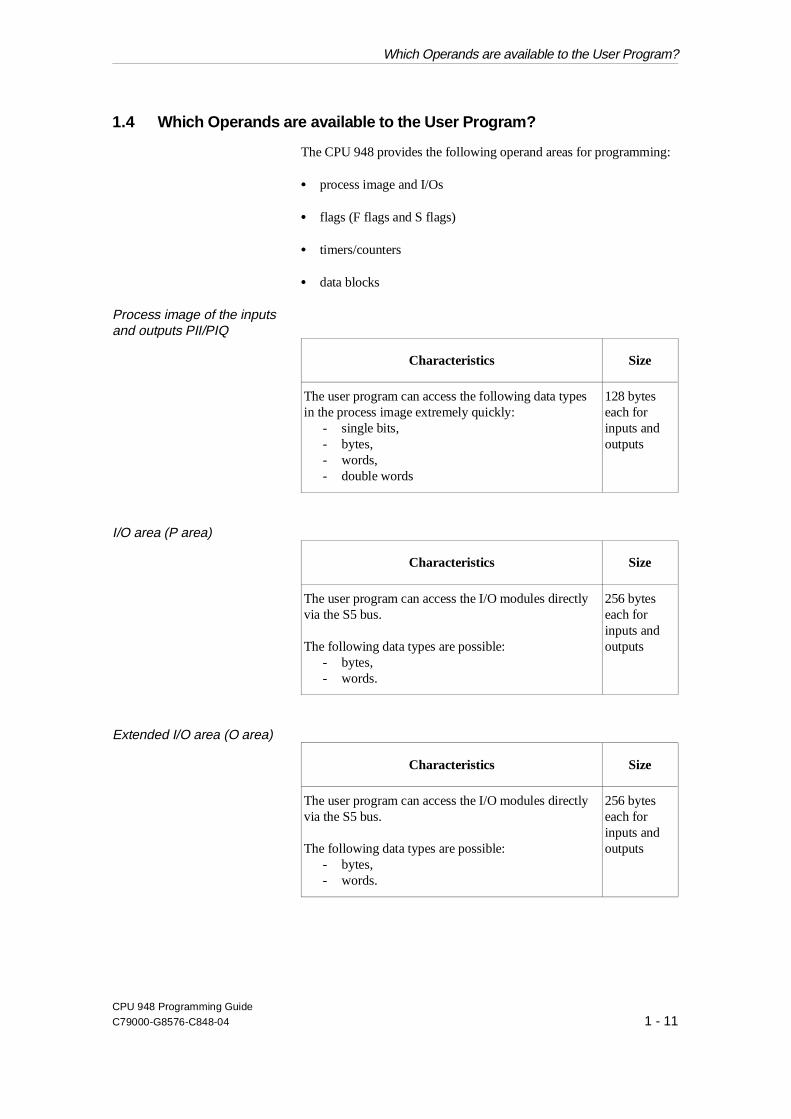
1.4 Which Operands are available to the User Program?
The CPU 948 provides the following operand areas for programming:
•• process image and I/Os
•• flags (F flags and S flags)
•• timers/counters
•• data blocks
Process image of the inputsand outputs PII/PIQ
Characteristics Size
The user program can access the following data typesin the process image extremely quickly:
- single bits, - bytes, - words, - double words
128 byteseach forinputs andoutputs
I/O area (P area)
Characteristics Size
The user program can access the I/O modules directlyvia the S5 bus.
The following data types are possible: - bytes,- words.
256 byteseach forinputs andoutputs
Extended I/O area (O area)
Characteristics Size
The user program can access the I/O modules directlyvia the S5 bus.
The following data types are possible: - bytes,- words.
256 byteseach forinputs andoutputs
Which Operands are available to the User Program?
CPU 948 Programming Guide
C79000-G8576-C848-04 1 - 11
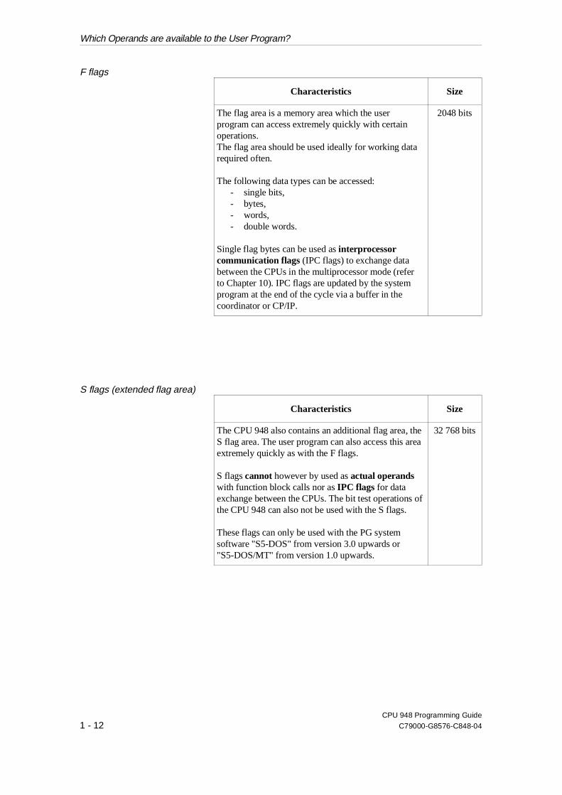
F flags
Characteristics Size
The flag area is a memory area which the userprogram can access extremely quickly with certainoperations.The flag area should be used ideally for working datarequired often.
The following data types can be accessed: - single bits, - bytes, - words, - double words.
Single flag bytes can be used as interprocessorcommunication flags (IPC flags) to exchange databetween the CPUs in the multiprocessor mode (referto Chapter 10). IPC flags are updated by the systemprogram at the end of the cycle via a buffer in thecoordinator or CP/IP.
2048 bits
S flags (extended flag area)
Characteristics Size
The CPU 948 also contains an additional flag area, theS flag area. The user program can also access this areaextremely quickly as with the F flags.
S flags cannot however by used as actual operandswith function block calls nor as IPC flags for dataexchange between the CPUs. The bit test operations ofthe CPU 948 can also not be used with the S flags.
These flags can only be used with the PG systemsoftware "S5-DOS" from version 3.0 upwards or"S5-DOS/MT" from version 1.0 upwards.
32 768 bits
Which Operands are available to the User Program?
CPU 948 Programming Guide
1 - 12 C79000-G8576-C848-04
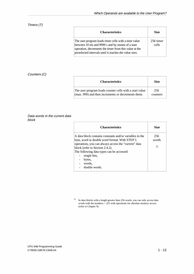
Timers (T)
Characteristics Size
The user program loads timer cells with a time valuebetween 10 ms and 9990 s and by means of a startoperation, decrements the timer from this value at thepreselected intervals until it reaches the value zero.
256 timercells
Counters (C)
Characteristics Size
The user program loads counter cells with a start value(max. 999) and then increments or decrements them.
256 counters
Data words in the current datablock
Characteristics Size
A data block contains constants and/or variables in thebyte, word or double word format. With STEP 5operations, you can always access the "current" datablock (refer to Section 2.4.2). The following data types can be accessed:
- single bits, - bytes,- words, - double words.
256 words
1)
1) In data blocks with a length greater than 256 words, you can only access datawords with the numbers > 255 with operations for absolute memory access(refer to Chapter 9).
Which Operands are available to the User Program?
CPU 948 Programming Guide
C79000-G8576-C848-04 1 - 13
1.5 How much Memory is available for the User Program?
For storing logic and data blocks, the CPU 948 only has the usermemory in the internal RAM.
The CPU 948 is available with two versions of the user memory:
•• Version 1: with 640 Kbytes,
•• Version 2: with 1,664 Kbytes.
How much Memory is available for the User Program?
CPU 948 Programming Guide
1 - 14 C79000-G8576-C848-04
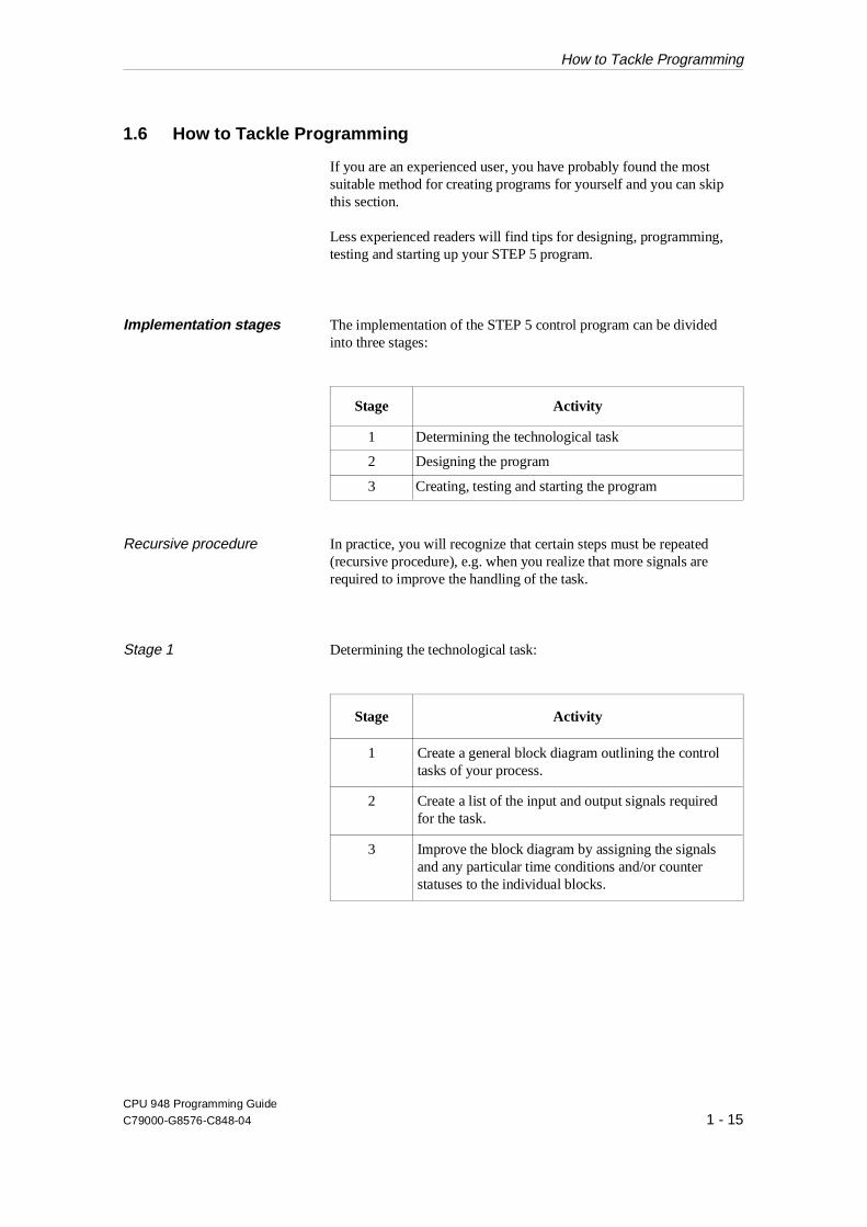
1.6 How to Tackle Programming
If you are an experienced user, you have probably found the mostsuitable method for creating programs for yourself and you can skipthis section.
Less experienced readers will find tips for designing, programming,testing and starting up your STEP 5 program.
Implementation stages The implementation of the STEP 5 control program can be dividedinto three stages:
Stage Activity
1 Determining the technological task
2 Designing the program
3 Creating, testing and starting the program
Recursive procedure In practice, you will recognize that certain steps must be repeated(recursive procedure), e.g. when you realize that more signals arerequired to improve the handling of the task.
Stage 1 Determining the technological task:
Stage Activity
1 Create a general block diagram outlining the controltasks of your process.
2 Create a list of the input and output signals requiredfor the task.
3 Improve the block diagram by assigning the signalsand any particular time conditions and/or counterstatuses to the individual blocks.
How to Tackle Programming
CPU 948 Programming Guide
C79000-G8576-C848-04 1 - 15
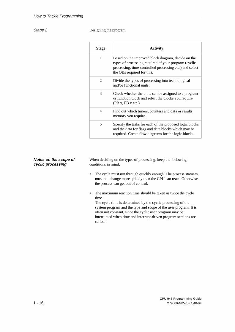
Stage 2 Designing the program
Stage Activity
1 Based on the improved block diagram, decide on thetypes of processing required of your program (cyclicprocessing, time-controlled processing etc.) and selectthe OBs required for this.
2 Divide the types of processing into technologicaland/or functional units.
3 Check whether the units can be assigned to a programor function block and select the blocks you require(PB x, FB y etc.)
4 Find out which timers, counters and data or resultsmemory you require.
5 Specify the tasks for each of the proposed logic blocksand the data for flags and data blocks which may berequired. Create flow diagrams for the logic blocks.
Notes on the scope ofcyclic processing
When deciding on the types of processing, keep the followingconditions in mind:
•• The cycle must run through quickly enough. The process statusesmust not change more quickly than the CPU can react. Otherwisethe process can get out of control.
•• The maximum reaction time should be taken as twice the cycletime.The cycle time is determined by the cyclic processing of thesystem program and the type and scope of the user program. It isoften not constant, since the cyclic user program may beinterrupted when time and interrupt-driven program sections arecalled.
How to Tackle Programming
CPU 948 Programming Guide
1 - 16 C79000-G8576-C848-04
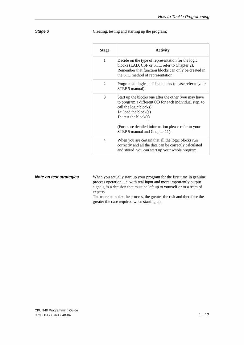
Stage 3 Creating, testing and starting up the program:
Stage Activity
1 Decide on the type of representation for the logicblocks (LAD, CSF or STL, refer to Chapter 2).Remember that function blocks can only be created inthe STL method of representation.
2 Program all logic and data blocks (please refer to yourSTEP 5 manual).
3 Start up the blocks one after the other (you may haveto program a different OB for each individual step, tocall the logic blocks):1a: load the block(s)1b: test the block(s)
(For more detailed information please refer to yourSTEP 5 manual and Chapter 11).
4 When you are certain that all the logic blocks runcorrectly and all the data can be correctly calculatedand stored, you can start up your whole program.
Note on test strategies When you actually start up your program for the first time in genuineprocess operation, i.e. with real input and more importantly outputsignals, is a decision that must be left up to yourself or to a team ofexperts.The more complex the process, the greater the risk and therefore thegreater the care required when starting up.
How to Tackle Programming
CPU 948 Programming Guide
C79000-G8576-C848-04 1 - 17

1.7 Programming Tools
Suitable PGs The following programmers are available for creating your userprogram, PG 685, PG 710, PG 730, PG 750 and PG 770. You cancheck on the performance and characteristics of these devices in thecatalog ST 59 /9/.
NoteIf you wish to use the full range of performance of the CPU 948in your automation software, (particularly the DX 0 screen, the"Output ISTACK" screen, the display with the "memoryconfiguration" function and the PG functions via the backplanebus) you require the PG system software "STEP 5/ST" fromversion 6.3 upwards or "STEP 5/MT" from version 6.0 upwardsplus the "Delta diskette CPU 948" and a PG 7xx.
Suitable software You can create user programs for SIMATIC S5 programmablecontrollers as follows:
•• In the STEP 5 programming language,
Here you require the STEP 5 programming package along with thesystem software STEP 5/ST or STEP 5/MT (description, refer to/3/ in Further Reading),
or
•• In a higher programming language:
If you are familiar with programming in higher programminglanguages, you can also formulate your STEP 5 program for theCPU 948 as follows:
- SCL (refer to /12/ in Further Reading, the SCL compiler iscontained in the PG software "S5-DOS/MT" from version 6upwards.) or
- C with S5 C compiler (refer to /13/ in Further Reading).
You can also create programs for sequence control systems in agraphic representation using the GRAPH 5 programming package(description, refer to /4/ in Further Reading).
Depending on the task, you can also incorporate "off-the-peg"standard function blocks in your user program. The performance andcharacteristics of these blocks are described in the catalog ST 57 /11/.
Programming Tools
CPU 948 Programming Guide
1 - 18 C79000-G8576-C848-04
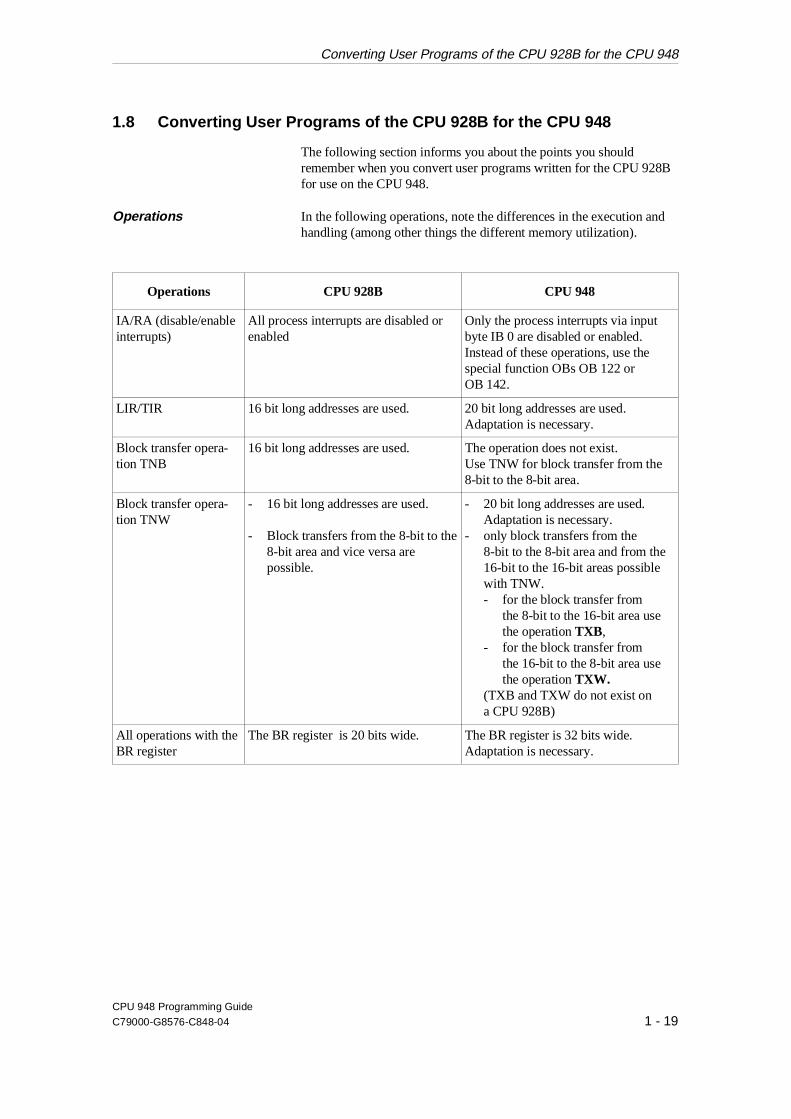
1.8 Converting User Programs of the CPU 928B for the CPU 948
The following section informs you about the points you shouldremember when you convert user programs written for the CPU 928Bfor use on the CPU 948.
Operations In the following operations, note the differences in the execution andhandling (among other things the different memory utilization).
Operations CPU 928B CPU 948
IA/RA (disable/enableinterrupts)
All process interrupts are disabled orenabled
Only the process interrupts via inputbyte IB 0 are disabled or enabled.Instead of these operations, use thespecial function OBs OB 122 orOB 142.
LIR/TIR 16 bit long addresses are used. 20 bit long addresses are used.Adaptation is necessary.
Block transfer opera-tion TNB
16 bit long addresses are used. The operation does not exist.Use TNW for block transfer from the8-bit to the 8-bit area.
Block transfer opera-tion TNW
- 16 bit long addresses are used.
- Block transfers from the 8-bit to the8-bit area and vice versa are possible.
- 20 bit long addresses are used.Adaptation is necessary.
- only block transfers from the8-bit to the 8-bit area and from the 16-bit to the 16-bit areas possible with TNW. - for the block transfer from
the 8-bit to the 16-bit area usethe operation TXB ,
- for the block transfer fromthe 16-bit to the 8-bit area usethe operation TXW.
(TXB and TXW do not exist on a CPU 928B)
All operations with theBR register
The BR register is 20 bits wide. The BR register is 32 bits wide. Adaptation is necessary.
Converting User Programs of the CPU 928B for the CPU 948
CPU 948 Programming Guide
C79000-G8576-C848-04 1 - 19
Timer processing
CPU 928B CPU 948
The timers are updated duringstart-up.
The timers are only updated inthe RUN mode(Reason: compatibility withCPU 946/947)
FB 0 as cycle block
CPU 928B CPU 948
If no cycle block OB 1 exists, thesystem program calls FB 0cyclically, provided it is loaded.
Only OB 1 can be used for cyclicprocessing. If you haveprogrammed FB 0, create anOB 1 in which FB 0 is called.
Default priorities
CPU 928B CPU 948
Process interrupts have higherpriority than timed interrupts.
Timed interrupts have priorityover process interrupts via IB 0or system interrupts. You canchange the priority with theparameters in DX 0.
Data block DB 0(block address list)
CPU 928B CPU 948
The block address list containsthe direct start addresses of theblocks.
The block address list containsthe segment addresses of theblocks. To obtain the startaddress of a block, its segmentaddress must be shifted 4 bits tothe left.
Converting User Programs of the CPU 928B for the CPU 948
CPU 948 Programming Guide
1 - 20 C79000-G8576-C848-04
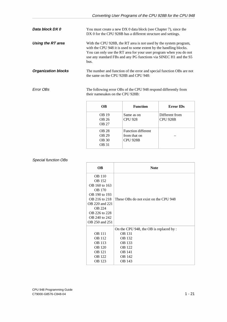
Data block DX 0 You must create a new DX 0 data block (see Chapter 7), since theDX 0 for the CPU 928B has a different structure and settings.
Using the RT area With the CPU 928B, the RT area is not used by the system program,with the CPU 948 it is used to some extent by the handling blocks.You can only use the RT area for your user program when you do notuse any standard FBs and any PG functions via SINEC H1 and the S5bus.
Organization blocks The number and function of the error and special function OBs are notthe same on the CPU 928B and CPU 948:
Error OBs The following error OBs of the CPU 948 respond differently fromtheir namesakes on the CPU 928B:
OB Function Error IDs
OB 19OB 26OB 27
Same as onCPU 928
Different fromCPU 928B
OB 28OB 29OB 30OB 31
Function differentfrom that onCPU 928B
–
Special function OBs
OB Note
OB 110OB 152
OB 160 to 163OB 170
OB 190 to 193OB 216 to 218
OB 220 and 221OB 224
OB 226 to 228OB 240 to 242
OB 250 and 251
These OBs do not exist on the CPU 948
OB 111OB 112OB 113OB 120OB 121OB 122OB 123
On the CPU 948, the OB is replaced by :OB 131OB 132OB 133OB 122OB 141OB 142OB 143
Converting User Programs of the CPU 928B for the CPU 948
CPU 948 Programming Guide
C79000-G8576-C848-04 1 - 21
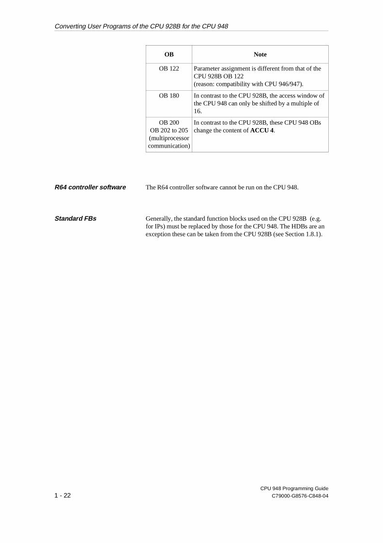
OB Note
OB 122 Parameter assignment is different from that of theCPU 928B OB 122 (reason: compatibility with CPU 946/947).
OB 180 In contrast to the CPU 928B, the access window ofthe CPU 948 can only be shifted by a multiple of16.
OB 200OB 202 to 205(multiprocessorcommunication)
In contrast to the CPU 928B, these CPU 948 OBschange the content of ACCU 4.
R64 controller software The R64 controller software cannot be run on the CPU 948.
Standard FBs Generally, the standard function blocks used on the CPU 928B (e.g.for IPs) must be replaced by those for the CPU 948. The HDBs are anexception these can be taken from the CPU 928B (see Section 1.8.1).
Converting User Programs of the CPU 928B for the CPU 948
CPU 948 Programming Guide
1 - 22 C79000-G8576-C848-04

Contents of Chapter 2
2.1 STEP 5 Programming Language . . . . . . . . . . . . . . . . . . . . . . . . . . . . . . . . . . . . . . . . . . . 2 - 4
2.1.1 The LAD, CSF, STL Methods of Representation . . . . . . . . . . . . . . . . . . . . . . . . . . . . . . 2 - 42.1.2 Structured Programming. . . . . . . . . . . . . . . . . . . . . . . . . . . . . . . . . . . . . . . . . . . . . . . . . . 2 - 52.1.3 STEP 5 Operations . . . . . . . . . . . . . . . . . . . . . . . . . . . . . . . . . . . . . . . . . . . . . . . . . . . . . . 2 - 62.1.4 Number Representation . . . . . . . . . . . . . . . . . . . . . . . . . . . . . . . . . . . . . . . . . . . . . . . . . . 2 - 82.1.5 STEP 5 Blocks and Storing them in Memory . . . . . . . . . . . . . . . . . . . . . . . . . . . . . . . . 2 - 12
2.2 Program, Organization and Sequence Blocks . . . . . . . . . . . . . . . . . . . . . . . . . . . . . . . . 2 - 16
2.2.1 Organization Blocks as User Interfaces . . . . . . . . . . . . . . . . . . . . . . . . . . . . . . . . . . . . . 2 - 182.2.2 Organization Blocks for Special Functions . . . . . . . . . . . . . . . . . . . . . . . . . . . . . . . . . . 2 - 22
2.3 Function Blocks . . . . . . . . . . . . . . . . . . . . . . . . . . . . . . . . . . . . . . . . . . . . . . . . . . . . . . . 2 - 23
2.3.1 Structure of Function Blocks . . . . . . . . . . . . . . . . . . . . . . . . . . . . . . . . . . . . . . . . . . . . . 2 - 242.3.2 Programming Function Blocks. . . . . . . . . . . . . . . . . . . . . . . . . . . . . . . . . . . . . . . . . . . . 2 - 262.3.3 Calling Function Blocks and Assigning Parameters to them . . . . . . . . . . . . . . . . . . . . 2 - 282.3.4 Special Function Blocks . . . . . . . . . . . . . . . . . . . . . . . . . . . . . . . . . . . . . . . . . . . . . . . . . 2 - 33
2.4 Data Blocks. . . . . . . . . . . . . . . . . . . . . . . . . . . . . . . . . . . . . . . . . . . . . . . . . . . . . . . . . . . 2 - 35
2.4.1 Creating Data Blocks . . . . . . . . . . . . . . . . . . . . . . . . . . . . . . . . . . . . . . . . . . . . . . . . . . . 2 - 372.4.2 Opening Data Blocks . . . . . . . . . . . . . . . . . . . . . . . . . . . . . . . . . . . . . . . . . . . . . . . . . . . 2 - 382.4.3 Special Data Blocks . . . . . . . . . . . . . . . . . . . . . . . . . . . . . . . . . . . . . . . . . . . . . . . . . . . . 2 - 41
2User Program
CPU 948 Programming Guide
C79000-G8576-C848-04 2 - 1

Contents
CPU 948 Programming Guide
2 - 2 C79000-G8576-C848-04
2User Program
The following chapter explains the components that make up aSTEP 5 user program for the CPU 948 and how it can be structured.
CPU 948 Programming Guide
C79000-G8576-C848-04 2 - 3

2.1 STEP 5 Programming Language
With the STEP 5 programming language, you convert automationtasks into programs that run on SIMATIC S5 programmablecontrollers. You can program simple binary functions, complexdigital functions and arithmetic operations including floatingpoint arithmetic using STEP 5.
Types of operation The operations of the STEP 5 programming language are divided intothe following groups:Basic operations
•• you can use these operations in all logic blocks
•• methods of representation: ladder diagram (LAD), control systemflowchart (CSF), statement list (STL).
Supplementary operations and system operations:
•• can only be used in function blocks
•• only statement list (STL) method of representation
•• system operations: only experienced STEP 5 programmers shoulduse system operations
2.1.1The LAD, CSF, STL Methods of Representation
When programming in STEP 5, you can choose between the threemethods of representation ladder diagram (LAD), control systemflowchart (CSF) and statement list (STL) for each individual logic block.You can choose the method of representation that best suits yourparticular application.The machine code MC5 that the programmers (PGs) generate is thesame for all three methods of representation. If you follow certain rules when programming in STEP 5 (see /3/), theprogrammer can translate your user program from one method ofrepresentation into any other.
Graphic representation or list of statements
While the ladder diagram (LAD) and control system flowchart (CSF)methods of representation represent your STEP 5 programgraphically, statement list (STL) represents STEP 5 operationsindividually as mnemonic abbreviations.
STEP 5 Programming Language
CPU 948 Programming Guide
2 - 4 C79000-G8576-C848-04
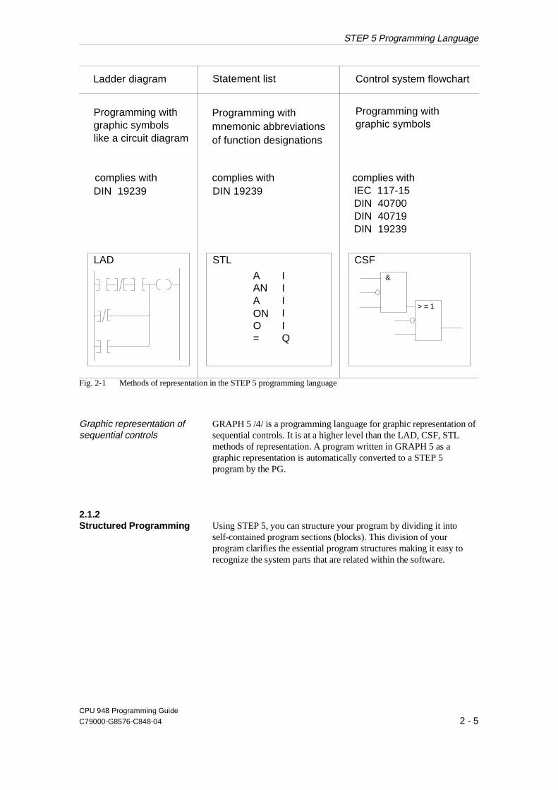
Graphic representation ofsequential controls
GRAPH 5 /4/ is a programming language for graphic representation ofsequential controls. It is at a higher level than the LAD, CSF, STLmethods of representation. A program written in GRAPH 5 as agraphic representation is automatically converted to a STEP 5program by the PG.
2.1.2Structured Programming Using STEP 5, you can structure your program by dividing it into
self-contained program sections (blocks). This division of yourprogram clarifies the essential program structures making it easy torecognize the system parts that are related within the software.
Ladder diagram Statement list Control system flowchart
Programming withgraphic symbolslike a circuit diagram
Programming withgraphic symbols
IEC 117-15DIN 40700DIN 40719DIN 19239
DIN 19239 DIN 19239
STL CSFLAD
AANAONO =
&
> = 1
IIIIIQ
Programming withmnemonic abbreviationsof function designations
complies with complies with complies with
Fig. 2-1 Methods of representation in the STEP 5 programming language
STEP 5 Programming Language
CPU 948 Programming Guide
C79000-G8576-C848-04 2 - 5
Structured programming offers you the following advantages:•• simple and clear creation of programs, even large ones
•• standardization of program parts
•• simple program organization
•• easy program changes
•• simple, section by section program test
•• simple system start-up
What is a block? A block is a part of the user program that is distinguished by itsfunction, structure or application. You can differentiate betweenblocks that contain statements (code) i.e. organization blocks,program blocks, function blocks or sequence blocks, and blocks thatcontain data (data blocks).
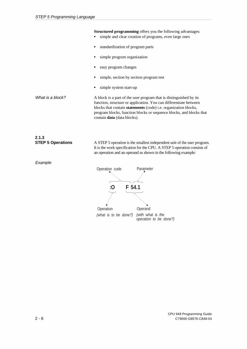
2.1.3STEP 5 Operations A STEP 5 operation is the smallest independent unit of the user program.
It is the work specification for the CPU. A STEP 5 operation consists ofan operation and an operand as shown in the following example:
Example
Operation code
Operation Operand
Parameter
:O F 54.1
(what is to be done?) (with what is theoperation to be done?)
STEP 5 Programming Language
CPU 948 Programming Guide
2 - 6 C79000-G8576-C848-04
Absolute and symbolicoperands
You can enter the operand absolutely or symbolically (using anassignment list) as shown in the following example: Absolute representation: :A I 1.4
Symbolic representation: :A -Motor1For more information on absolute and symbolic programming, refer toyour STEP 5 manual.
Application of STEP 5 operations
The STEP 5 operation set enables you to do the following:
•• set or reset and combine binary values logically
•• load and transfer values
•• compare values and process them arithmetically
•• specify timer and counter values
•• convert number representations
•• call blocks and execute jumps within a block
and
•• influence program execution
Result of logic operation RLO The central bit for controlling the program is the result of logicoperation RLO. This is obtained as a result of binary logic operationsand is influenced by some operations.Section 3.5 describes the whole STEP 5 operation set and explains howthe RLO is obtained. This section also includes programming examplesfor individual STEP 5 operations.
STEP 5 Programming Language
CPU 948 Programming Guide
C79000-G8576-C848-04 2 - 7
2.1.4Number Representation To allow the CPU to logically combine, modify or compare numerical
values, these values must be located in the accumulators (workingregisters of the CPU) as binary numbers. Depending on the operations to be carried out, the following numberrepresentations are permitted in STEP 5:Binary numbers: 16-bit fixed point numbers
32-bit fixed point numbers
32-bit floating point numbers (with a 24-bit mantissa)
Decimal numbers: BCD-coded numbers (sign and 3 digits)
Numerical input on the PG When you use a programmer to input or display number values, youset the data format on the programmer (e.g. KF or fixed point) inwhich you intend to enter or display the values. The programmerconverts the internal representation into the form you have requested.
Permitted operations You can carry out all arithmetic operations with the 16-bit fixedpoint numbers and floating point numbers, including comparison,addition, subtraction, multiplication and division.
NoteDo not use BCD-coded numbers for arithmetical operations, sincethis leads to incorrect results.
Use 32-bit fixed point numbers to execute comparison operations.These are also necessary as an intermediate level when convertingnumbers in BCD code to floating point numbers. With the operations+D and -D they can also be used for addition and subtraction.The STEP 5 programming language also has conversion operations thatenable you to convert numbers directly to the most important of the othernumerical representations.
STEP 5 Programming Language
CPU 948 Programming Guide
2 - 8 C79000-G8576-C848-04
16-bit and 32-bit fixedpoint numbers
Fixed point numbers are whole binary numbers with a sign.
Coding of fixed point numbers Fixed point numbers are 16 bit (= 1 word) or 32 bit (= 2 words) inbinary representation. Bit 15 or bit 31 contains the sign.•• ’0’ = positive number
•• ’1’ = negative numberThe two’s complement representation is used for negative numbers.
PG input Input of 16-bit fixed point number data format at the PG:KF
Input of 32-bit fixed point number data format at the PG:DH
Permitted numerical range 16-bit fixed point number-32768 to +32767 (16 bits)
32-bit fixed point number-2147483648 to +2147483647 (32 bits) (8000 0000H to 7FFF FFFFH)
Using fixed point numbers Use fixed point numbers for simple calculations and for comparingnumber values. Since fixed point numbers are always whole numbers,remember that the result of dividing two fixed point numbers is also afixed point number without decimal places.
Floating point numbers Floating point numbers are positive and negative fractions. Theyalways occupy a double word (32 bits). A floating point number isrepresented as an exponential number. The mantissa is 24 bits longand the exponent is 8 bits long.In the CPU 948, the default mantissa is 24 bits long (bits 0 to 23) foradding, subtracting, multiplying and dividing.The exponent indicates the order of magnitude of the floating pointnumber. The sign of the exponent tells you whether the value of thefloating point number is greater or less than 0.1.
STEP 5 Programming Language
CPU 948 Programming Guide
C79000-G8576-C848-04 2 - 9
Using floating point numbers Use floating point numbers for solving extensive calculations,especially for multiplication and division or when you are workingwith very large or very small numbers!
Accuracy The mantissa indicates the accuracy of the floating point number asfollows:•• Accuracy with a 24-bit mantissa:
2-24 = 0.000000059604 (corresponds to 7 decimal places)If the sign of the mantissa is "0" the number is positive; if the sign is"1" it is a negative number in its two’s complement representation.The floating point value ’0’ is represented as the binary value80000000H (32 bits, see below).
Coding floating point numbers Coding a floating point number:
31 30 24 23 22 0
V 26 ... . ... 20 V 2-1 .... . . . . . ... 2-23
Exponent Mantissa
Specification of the data format for floating point numbers at thePG: KG
Permissible numerical range ± 0.1469368 x 10-38 to ± 0.1701412 x 1039
Input/output on PG a) in a logic block:
You want to load the number N = 12.34567 as a floating point number.
Input:
:LKG1234567+2
STEP 5 Programming Language
CPU 948 Programming Guide
2 - 10 C79000-G8576-C848-04
b) in a data block:
You want to define the number N = - 0.005 as a floating point constant.
Input:
6: KG = - 5 - 2
Numbers in BCD code Decimal numbers are represented as numbers in BCD code. With theirsign and three digits, they occupy 16 bits (1 word) in an accumulatoras shown in the following example: 15 12 11 8 7 4 3 0
V V V V hundreds tens ones
The individual digits are positive 4-bit binary numbers between 0000 and1001 (0 and 9 decimal).The left bits are reserved for the sign as follows:Sign for a positive number: 0000Sign for a negative number: 1111
Permissible numerical range -999 to +999
PG display after you enter the line:
:L KG + 1234567 + 02
Mantissa with sign Exponent (base 10) with sign
Value of the number input: +0.1234567 x 10+2 = 12.34567
PG display after you enter the line:
6: KG =- 5000000 - 02
Mantissa with sign Exponent (base 10) with sign
Value of the number input : - 0.5 x 10-2 = 0.005
STEP 5 Programming Language
CPU 948 Programming Guide
C79000-G8576-C848-04 2 - 11
2.1.5STEP 5 Blocks and Storingthem in Memory
Identification A block is identified as follows: •• the block type (OB, PB, SB, FB, FX, DB, DX)
and
•• the block number (number between 0 and 255).
Block types The STEP 5 programming language differentiates between thefollowing block types:
Organization blocks (OB) Organization blocks are the interface between the system program andthe user program. They can be divided into two groups as follows:
With OB 1 to OB 39, you can control program execution, the restartprocedure of the CPU and the reaction in the event of an error. Youprogram these blocks yourself according to your automation task.These OBs are called by the system program.
OBs 40 to 100 are blocks belonging to the operating system. Youmust not call these blocks.
OBs 121 to 255 contain special functions of the system program. Youcan call these blocks, if required, in your user program.
Program blocks (PB) You require program blocks to structure your program. They containprogram parts divided according to technological and functionalcriteria. Program blocks represent the heart of the user program.
Sequence blocks (SB) Sequence blocks were originally special program blocks for step bystep processing of sequencers. In the meantime, however, sequencerscan be programmed with GRAPH 5/4/. Sequence blocks havetherefore lost their original significance in STEP 5.Sequence blocks now represent an extension of the program blocksand are used as program blocks.
STEP 5 Programming Language
CPU 948 Programming Guide
2 - 12 C79000-G8576-C848-04
Function blocks (FB/FX) You use function blocks to program frequently recurring and/orcomplex functions (e.g. digital functions, sequence control systems,closed loop controls and signalling functions).
A function block can be called several times by higher order blocksand supplied with new operands (assigned parameters) at each call.Using block type FX doubles the maximum number of possible functionblocks.
Data blocks (DB/DX) Data blocks contain the (fixed or variable) data with which the userprogram works. This type of block contains no STEP 5 statements andhas a distinctly different function from the other blocks. Using blocktype DX doubles the number of possible data blocks.
Formal structure of the blocks
All blocks consist of the following two parts:
•• a block header
and
•• a block body
Block header The block header is always 5 words long and contains information forblock management in the PG and data for the system program.
Block body Depending on the block type, the block body contains the following: •• STEP-5 operations (in OB, PB, SB, FB, FX),
•• variable or constant data (in DB, DX)
and
•• a formal operand list (in FB, FX).
STEP 5 Programming Language
CPU 948 Programming Guide
C79000-G8576-C848-04 2 - 13

Block preheader The programmer also generates a block preheader (DV, DXV, FV,FXV) for block types DB, DX, FB and FX. These block preheaderscontain information about the data format (for DB and DX) or thejump labels (for FB and FX). Only the PG can evaluate thisinformation. Consequently the block preheaders are not transferred tothe CPU memory. You cannot influence the contents of the blockheader directly.
Maximum length A STEP-5 block can occupy a maximum of 32 767 words in theprogram memory of the CPU (1 word corresponds to 16 bits).
Available blocks
You can program the following block types:
Data blocks DB 0, DB 1, DB 2, DX 0, DX 1 and DX 2 containparameters. These are reserved for specific functions and you cannot usethem as normal data blocks.Data block DX 2 is reserved for the 2nd serial interface and you shouldnot use it.
OB 1 to 39
FB 0 to 255 total 512
FX 0 to 255
PB 0 to 255
SB 0 to 255
DB 2 to 255 total 508
DX 3 to 255
STEP 5 Programming Language
CPU 948 Programming Guide
2 - 14 C79000-G8576-C848-04
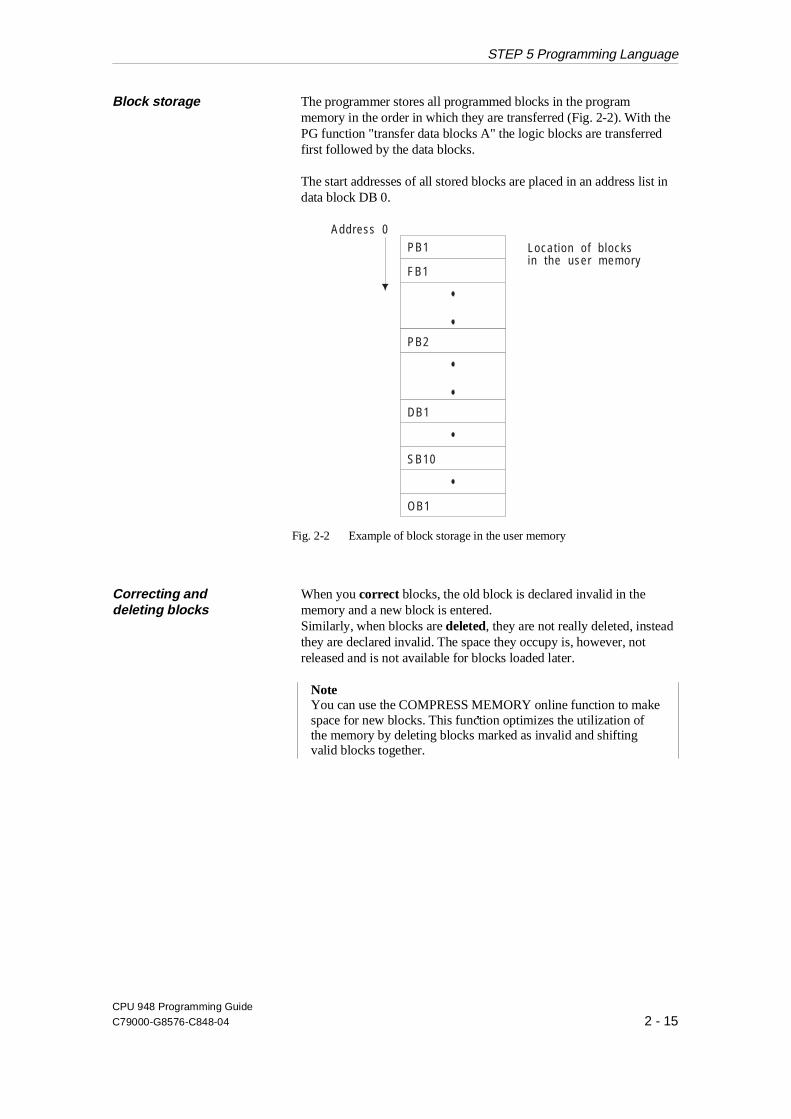
Block storage The programmer stores all programmed blocks in the programmemory in the order in which they are transferred (Fig. 2-2). With thePG function "transfer data blocks A" the logic blocks are transferredfirst followed by the data blocks. The start addresses of all stored blocks are placed in an address list indata block DB 0.
Correcting and deleting blocks
When you correct blocks, the old block is declared invalid in thememory and a new block is entered.Similarly, when blocks are deleted, they are not really deleted, insteadthey are declared invalid. The space they occupy is, however, notreleased and is not available for blocks loaded later.
NoteYou can use the COMPRESS MEMORY online function to makespace for new blocks. This function optimizes the utilization ofthe memory by deleting blocks marked as invalid and shiftingvalid blocks together.
Locat ion of blocksin the user memory
Address 0
FB1
OB1
SB10
DB1
PB1
PB2
Fig. 2-2 Example of block storage in the user memory
STEP 5 Programming Language
CPU 948 Programming Guide
C79000-G8576-C848-04 2 - 15
2.2 Program, Organization and Sequence Blocks
Program blocks (PBs), organization blocks (OBs) and sequenceblocks (SBs) are the same with respect to programming and calling.You can program all three types in the LAD, CSF and STL methodsof representation.
Programming When programming organization, program and sequence blocks,proceed as follows:
Step Action
1 First indicate the type of block and then the number of theblock that you want to program.
The following numbers are available for the type of block listed:
- program blocks 0 to 255- sequence blocks 0 to 255- organization blocks 1 to 39
2 Enter your program in the STEP 5 programming language.
When programming PBs, OBs and SBs, you can only use the STEP 5 basic operations!
A STEP 5 block should always be a self-containedprogram section. Logic operations must always be completedwithin a block.
3 Complete your program input with the block endoperation "BE".
Block calls With the exception of OB 1 to OB 39 you must call the blocks toprocess them. Use the special STEP 5 block call operations to call theblocks. You can program block calls inside an organization, program,function or sequence block. They can be compared with jumps to asubroutine. Each jump causes a block change. The return addresswithin the calling block is buffered by the system.
Program, Organization and Sequence Blocks
CPU 948 Programming Guide
2 - 16 C79000-G8576-C848-04

Block calls can be unconditional or conditional as follows:Unconditional call The "JU" statement belongs to the unconditional operations. It has no
effect on the RLO. The RLO is carried along with the jump to the newblock. Within the new block, it can be evaluated but no longercombined logically.
The addressed block is processed regardless of the previous result oflogic operation (RLO - see Section 3.4).
Example: JU PB 100
Conditional call The JC statement belongs to the conditional operations. The addressedblock is processed only if the previous RLO = 1. If the RLO = 0, thejump is not executed.
Example: JC PB 100
NoteAfter the conditional jump operation is executed, the RLO is setto "1" regardless of whether or not the jump to the block isexecuted.
PB 1 PB 5 PB 10
PB 6
BE
BE
BE
BE
A A
O
I 1.0 I 2.0
I 3.0
JU PB 5O I 5.3
A I 1.5JC PB 6A I 3.2
JC PB 10O F 1.5
Fig. 2-3 Block calls that enable processing of a program block
Program, Organization and Sequence Blocks
CPU 948 Programming Guide
C79000-G8576-C848-04 2 - 17
Effect of the BE statement After the "BE" statement (block end), the CPU continues the userprogram in the block in which the block call was programmed.Program execution continues at the STEP 5 statement following theblock call.The "BE" statement is executed regardless of the RLO. After "BE",the RLO can no longer be combined logically. However, the RLO orarithmetic result occurring directly before execution of the BEoperation is transferred to the block where the call originated and canbe evaluated there. When program execution returns from the blockthat has been called, the contents of ACCU 1, ACCU 2, ACCU 3 andACCU 4, the condition codes CC 0 and CC 1 and the RLO are notchanged. (Refer to Section 3.5 for more detailed information about theACCUs, CC0/CC1 and RLO).
2.2.1Organization Blocks asUser Interfaces
Organization blocks form the interfaces between the system programand the user program. Organization blocks OB 1 to OB 39 belong toyour user program just as program blocks. By programming theseOBs, you can influence the behavior of the CPU during start-up,program execution and in the event of an error. The organizationblocks are effective as soon as they are loaded in the PLC memory.This is also possible while the PLC is in the run mode.Once the system program has called a specific organization block, theuser program it contains is executed.
NoteYou can program blocks OB 1 to OB 39 as user interfaces andthey are called automatically by the system program as a reactionto certain events.
For test purposes, you can also call these organization blocksfrom the user program (JC/JU OB xxx). It is, however, notpossible to trigger a COLD RESTART, e.g. by calling OB 20.
The following table provides you with an overview of the userinterfaces (OBs).
Program, Organization and Sequence Blocks
CPU 948 Programming Guide
2 - 18 C79000-G8576-C848-04
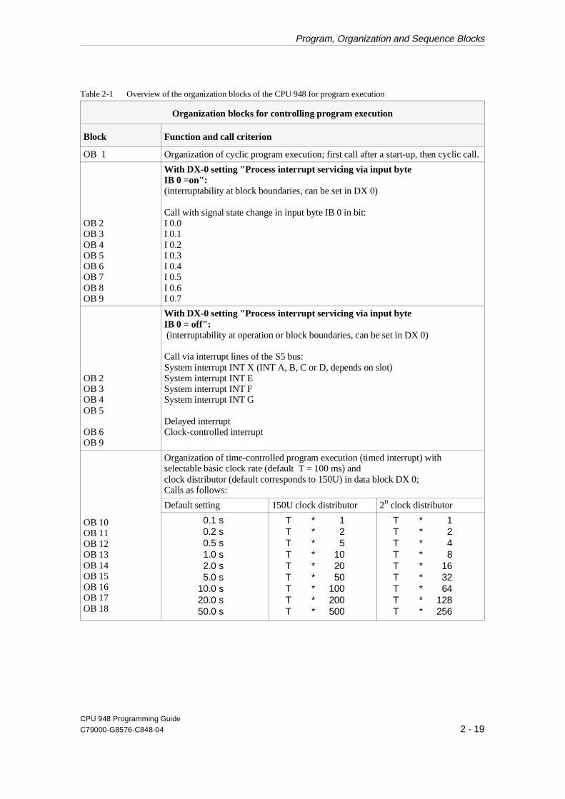
Organization blocks for controlling program execution
Block Function and call criterion
OB 1 Organization of cyclic program execution; first call after a start-up, then cyclic call.
OB 2OB 3OB 4OB 5OB 6OB 7OB 8OB 9
With DX-0 setting "Process interrupt servicing via input byte IB 0 =on":(interruptability at block boundaries, can be set in DX 0)
Call with signal state change in input byte IB 0 in bit:I 0.0I 0.1I 0.2I 0.3I 0.4I 0.5I 0.6I 0.7
OB 2OB 3OB 4OB 5
OB 6OB 9
With DX-0 setting "Process interrupt servicing via input byte IB 0 = off": (interruptability at operation or block boundaries, can be set in DX 0)
Call via interrupt lines of the S5 bus:System interrupt INT X (INT A, B, C or D, depends on slot)System interrupt INT ESystem interrupt INT FSystem interrupt INT G
Delayed interruptClock-controlled interrupt
OB 10OB 11OB 12OB 13OB 14OB 15OB 16OB 17OB 18
Organization of time-controlled program execution (timed interrupt) withselectable basic clock rate (default T = 100 ms) andclock distributor (default corresponds to 150U) in data block DX 0;Calls as follows:
Default setting 150U clock distributor 2n clock distributor
0.1 s0.2 s0.5 s1.0 s2.0 s5.0 s
10.0 s20.0 s50.0 s
T * 1T * 2T * 5T * 10T * 20T * 50T * 100T * 200T * 500
T * 1T * 2T * 4T * 8T * 16T * 32T * 64T * 128T * 256
Table 2-1 Overview of the organization blocks of the CPU 948 for program execution
Program, Organization and Sequence Blocks
CPU 948 Programming Guide
C79000-G8576-C848-04 2 - 19

Organization blocks to control the start-up procedure
Block Function and call criterion
OB 20 Call on request for COLD RESTART (manual and automatic)
OB 21 Call on request for MANUAL WARM RESTART/COLD RESTART WITHMEMORY
OB 22 Call on request for AUTOMATIC WARM RESTART/COLD RESTARTWITH MEMORY
Organization blocks to control the start-up procedure
Block Function and call criterion
OB 38 Organization of the start-up procedure for communication in the"soft stop" mode.
OB 39 Organization of the cyclic program for communication in the "soft stop" mode.
Organization blocks for reaction to device or program errors 1)
Block Function and call criterion
OB 19 Runtime error (LZF): called block not loaded (PB, SB, FB, FX) or attempt to open a data block that is not loaded (DB, DX)
OB 23 Timeout (QVZ) in user program (during direct access to I/O modules)
OB 24 Timeout (QVZ) when updating the process image and transferring interprocessor communication flags.
OB 25 Addressing error (ADF)
OB 26 Cycle time exceeded (ZYK)
Table 2-4 continued:
OB 27 Substitution error (SUF)
Table 2-2 Overview of the organization blocks of the CPU 948 for start-up
Table 2-3 Organization blocks of the CPU 948 for a SOFT STOP
Table 2-4 Overview of the organization blocks of the CPU 948 for error handling
Program, Organization and Sequence Blocks
CPU 948 Programming Guide
2 - 20 C79000-G8576-C848-04
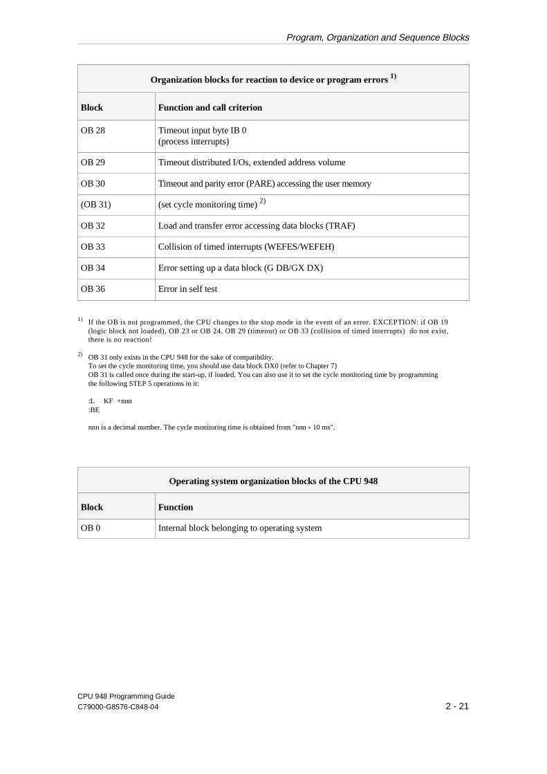
Organization blocks for reaction to device or program errors 1)
Block Function and call criterion
OB 28 Timeout input byte IB 0(process interrupts)
OB 29 Timeout distributed I/Os, extended address volume
OB 30 Timeout and parity error (PARE) accessing the user memory
(OB 31) (set cycle monitoring time) 2)
OB 32 Load and transfer error accessing data blocks (TRAF)
OB 33 Collision of timed interrupts (WEFES/WEFEH)
OB 34 Error setting up a data block (G DB/GX DX)
OB 36 Error in self test
1) If the OB is not programmed, the CPU changes to the stop mode in the event of an error. EXCEPTION: if OB 19(logic block not loaded), OB 23 or OB 24, OB 29 (timeout) or OB 33 (collision of timed interrupts) do not exist, there is no reaction!
2) OB 31 only exists in the CPU 948 for the sake of compatibility.To set the cycle monitoring time, you should use data block DX0 (refer to Chapter 7)OB 31 is called once during the start-up, if loaded. You can also use it to set the cycle monitoring time by programmingthe following STEP 5 operations in it:
:L KF +nnn:BE
nnn is a decimal number. The cycle monitoring time is obtained from "nnn * 10 ms".
Operating system organization blocks of the CPU 948
Block Function
OB 0 Internal block belonging to operating system
Program, Organization and Sequence Blocks
CPU 948 Programming Guide
C79000-G8576-C848-04 2 - 21
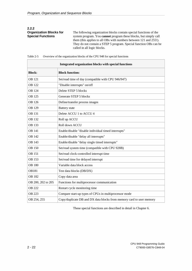
2.2.2Organization Blocks for Special Functions
The following organization blocks contain special functions of thesystem program. You cannot program these blocks, but simply callthem (this applies to all OBs with numbers between 121 and 255!).They do not contain a STEP 5 program. Special function OBs can becalled in all logic blocks.
Integrated organization blocks with special functions
Block: Block function:
OB 121 Set/read time of day (compatible with CPU 946/947)
OB 122 "Disable interrupts" on/off
OB 124 Delete STEP 5 blocks
OB 125 Generate STEP 5 blocks
OB 126 Define/transfer process images
OB 129 Battery state
OB 131 Delete ACCU 1 to ACCU 4
OB 132 Roll up ACCU
OB 133 Roll down ACCU
OB 141 Enable/disable "disable individual timed interrupts"
OB 142 Enable/disable "delay all interrupts"
OB 143 Enable/disable "delay single timed interrupts"
OB 150 Set/read system time (compatible with CPU 928B)
OB 151 Set/read clock-controlled interrupt time
OB 153 Set/read time for delayed interrupt
OB 180 Variable data block access
OB181 Test data blocks (DB/DX)
OB 182 Copy data area
OB 200, 202 to 205 Functions for multiprocessor communication
OB 222 Restart cycle monitoring time
OB 223 Compare start-up types of CPUs in multiprocessor mode
OB 254, 255 Copy/duplicate DB and DX data blocks from memory card to user memory
These special functions are described in detail in Chapter 6.
Table 2-5 Overview of the organization blocks of the CPU 948 for special functions
Program, Organization and Sequence Blocks
CPU 948 Programming Guide
2 - 22 C79000-G8576-C848-04
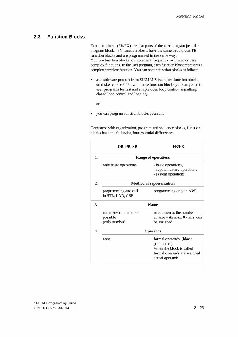
2.3 Function Blocks
Function blocks (FB/FX) are also parts of the user program just likeprogram blocks. FX function blocks have the same structure as FBfunction blocks and are programmed in the same way.You use function blocks to implement frequently recurring or verycomplex functions. In the user program, each function block represents acomplex complete function. You can obtain function blocks as follows:
•• as a software product from SIEMENS (standard function blockson diskette - see /11/); with these function blocks you can generateuser programs for fast and simple open loop control, signalling,closed loop control and logging;
or
•• you can program function blocks yourself.
Compared with organization, program and sequence blocks, functionblocks have the following four essential differences:
OB, PB, SB FB/FX
1. Range of operations
only basic operations - basic operations, - supplementary operations- system operations
2. Method of representation
programming and call in STL, LAD, CSF
programming only in AWL
3. Name
name environment notpossible(only number)
in addition to the numbera name with max. 8 chars. canbe assigned
4. Operands
none formal operands (block parameters).When the block is calledformal operands are assignedactual operands
Function Blocks
CPU 948 Programming Guide
C79000-G8576-C848-04 2 - 23

2.3.1Structure of Function Blocks The block header (five words) of a function block has the same
structure as the headers of the other STEP 5 block types.
The block body on the other hand, has a different structure from thebodies of the other block types. The block body contains the functionto be executed in the form of a statement list in the STEP 5programming language. Between the block header and the STEP 5statements, the function block needs additional memory space for itsname and for a list of formal operands. Since this list contains nostatements for the CPU, it is skipped with an unconditional jump thatthe programmer generates automatically. This jump statement is notdisplayed when the function block is displayed on the PG!
When a function block is called, only the block body is processed.
Absolute or symbolic operands
You can enter operands in a function block in absolute form (e.g. F 2.5) or symbolically (e.g. MOTOR1). You must store theassignment of the symbolic operands in an assignment list before youenter the operands in a function block (see /3/).
Fig. 2-4 shows the structure of a function block in the memory of aprogrammable controller.
JU
Name of the FB/FX
Formal operand 1
Formal operand 2
Formal operand n
5 words
1 word
4 words
3 words
Blockheader
Blockbody
BE
3 words
Skip formaloperandl ist
1st STEP 5 user operat ion
3 words
List offormaloperands
STEP 5userprogram
Fig. 2-4 Structure of a function block (FB/FX)
Function Blocks
CPU 948 Programming Guide
2 - 24 C79000-G8576-C848-04
The memory contains all the information that the programmer needsto represent the function block graphically when it is called and tocheck the operands during parameter assignment and programming ofthe function block. The programmer rejects incorrect input.
When handling function blocks, distinguish between the followingprocedures:
•• programming FB/FX
and
•• calling FB/FX and then assigning actual values to the parameters.
Distinction: "programming" – "calling and assigning parameters"
When programming, you specify the function of the block. You mustdecide which input operands the function requires and which outputresults it should transfer to the calling program. You define the inputoperands and output results as formal operands. These function astokens.
When a block is called by a higher order block (OB, PB, SB, FB, FX),the formal operands (block parameters) are replaced by actual operands;i.e. parameters are assigned to the function block.
How to program
IF... THEN...
You want to program a functionblock "directly", i.e. withoutformal operands.
Program it as you would aprogram or sequence block.
You want to use formal operands in a function block.
Proceed as explained on thefollowing pages.Make sure you keep to therequired order:First program the FB/FX with theformal operands and keep it on the PG (offline) or in the CPUmemory (online)Then program the block(s) to becalled with the actual operands.
Function Blocks
CPU 948 Programming Guide
C79000-G8576-C848-04 2 - 25

2.3.2Programming Function Blocks
You can program a function block only in the "statement list"method of representation. When entering a function block at aprogrammer, perform the following steps:
Step Action
1 Enter the block type (FB/FX) and the number of thefunction block.
Number your function blocks in descending orderstarting with FB 255, so that they do not collide withthe standard function blocks. The standard functionblocks are numbered from FB 1 to FB 199.
2 Enter the name of the function block.
The name can have a maximum of eight characters and must start with a letter.
3 If the function block is to process formal operands:Enter the formal operands you require in the block asblock parameters.
Enter the following information for each formal operand:
- the name of the block parameter (maximum 4 characters),
- the type of block parameter and the data type of the block parameter (if applicable)
You can define a maximum of 40 formal operands.
4 Enter your STEP 5 program in the form of a statementlist (STL). The formal operands are preceded by anequality sign (e.g. A = X1). They can also be referencedmore than once at various positions in the function block.
5 Terminate your program input with the block end operation "BE".
Function Blocks
CPU 948 Programming Guide
2 - 26 C79000-G8576-C848-04
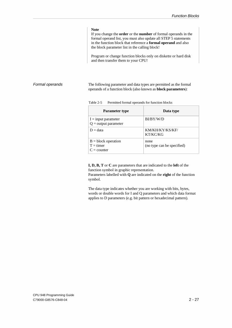
NoteIf you change the order or the number of formal operands in theformal operand list, you must also update all STEP 5 statementsin the function block that reference a formal operand and alsothe block parameter list in the calling block!
Program or change function blocks only on diskette or hard diskand then transfer them to your CPU!
Formal operands The following parameter and data types are permitted as the formaloperands of a function block (also known as block parameters):
Parameter type Data type
I = input parameterQ = output parameter
BI/BY/W/D
D = data KM/KH/KY/KS/KF/KT/KC/KG
B = block operationT = timerC = counter
none(no type can be specified)
I, D, B, T or C are parameters that are indicated to the left of thefunction symbol in graphic representation.Parameters labelled with Q are indicated on the right of the functionsymbol.
The data type indicates whether you are working with bits, bytes,words or double words for I and Q parameters and which data formatapplies to D parameters (e.g. bit pattern or hexadecimal pattern).
Table 2-5 Permitted formal operands for function blocks
Function Blocks
CPU 948 Programming Guide
C79000-G8576-C848-04 2 - 27
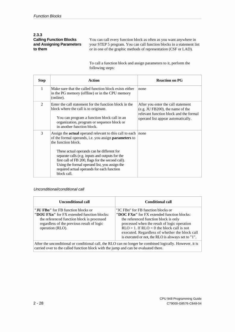
2.3.3Calling Function Blocks and Assigning Parameters to them
You can call every function block as often as you want anywhere inyour STEP 5 program. You can call function blocks in a statement listor in one of the graphic methods of representation (CSF or LAD).
To call a function block and assign parameters to it, perform thefollowing steps:
Step Action Reaction on PG
1 Make sure that the called function block exists eitherin the PG memory (offline) or in the CPU memory(online).
none
2 Enter the call statement for the function block in the block where the call is to originate.
You can program a function block call in anorganization, program or sequence block orin another function block.
After you enter the call statement (e.g. JU FB200), the name of the relevant function block and the formaloperand list appear automatically.
3 Assign the actual operand relevant to this call to eachof the formal operands, i.e. you assign parameters tothe function block.
These actual operands can be different for separate calls (e.g. inputs and outputs for thefirst call of FB 200, flags for the second call).Using the formal operand list, you assign the required actual operands for each functionblock call.
none
Unconditional/conditional call
Unconditional call Conditional call
"JU FBn" for FB function blocks or "DOU FXn" for FX extended function blocks:
the referenced function block is processedregardless of the previous result of logicoperation (RLO).
"JC FBn" for FB function blocks or "DOC FXn" for FX extended function blocks:
the referenced function block is onlyprocessed when the result of logic operationRLO = 1. If RLO = 0 the block call is notexecuted. Regardless of whether the block callis executed or not, the RLO is alsways set to "1".
After the unconditional or conditional call, the RLO can no longer be combined logically. However, it iscarried over to the called function block with the jump and can be evaluated there.
Function Blocks
CPU 948 Programming Guide
2 - 28 C79000-G8576-C848-04

Permitted actual operands Which operands can be assigned as actual operands is shown in thefollowing table.
Parametertype
Data type Actual operands permitted
I, Q BI for an operandwith bit address
BY for an operandwith byte address
W for an operandwith word address
D for an operandwith double word address
I n.m inputQ n.m outputF n.m flag
IB n input byteQB n output byteFY n flag byte DL n data byte leftDR n data byte rightPY n peripheral byteOY n byte from extended periphery
IW n input wordQW n output wordFW n flag wordDW n data wordPW n peripheral wordOW n word from extended periphery
ID n input double wordQD n output double wordFD n flag double wordDD n data double word
D KM for a binary pattern (16 bits)
KY for two absolute numbers,one byte each, each in therange from 0 to 255
KH for a hexadecimal patternwith a maximum of four digits
KS for two alphanumericcharacters
KT for timer value (BCD-coded) units .0 to .3 and values 0 to 999
KC for a counter value0 to 999
Constants
Table 2-6 Permitted actual operands for function blocks
Function Blocks
CPU 948 Programming Guide
C79000-G8576-C848-04 2 - 29
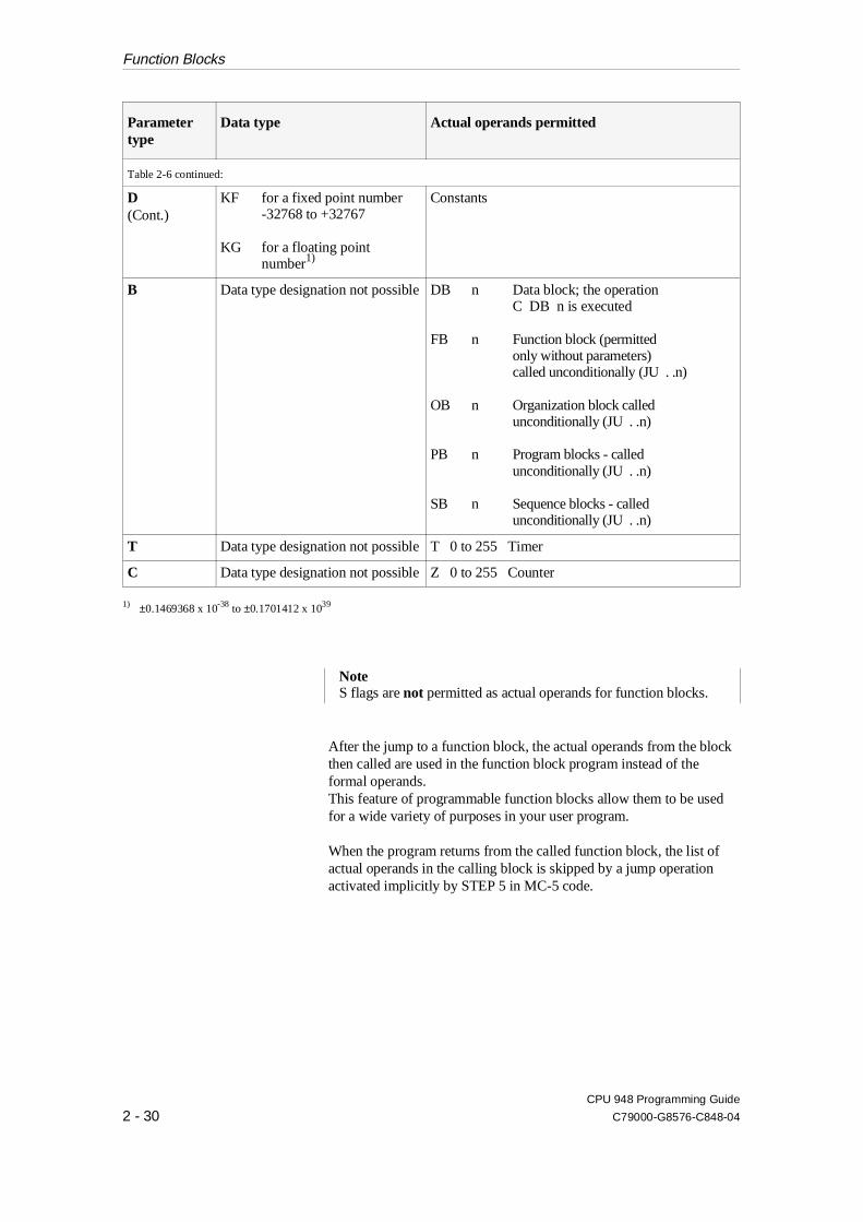
Parametertype
Data type Actual operands permitted
Table 2-6 continued:
D(Cont.)
KF for a fixed point number-32768 to +32767
KG for a floating point number1)
Constants
B Data type designation not possible DB n Data block; the operationC DB n is executed
FB n Function block (permitted only without parameters)called unconditionally (JU . .n)
OB n Organization block calledunconditionally (JU . .n)
PB n Program blocks - calledunconditionally (JU . .n)
SB n Sequence blocks - called unconditionally (JU . .n)
T Data type designation not possible T 0 to 255 Timer
C Data type designation not possible Z 0 to 255 Counter
1) ±0.1469368 x 10-38 to ±0.1701412 x 1039
NoteS flags are not permitted as actual operands for function blocks.
After the jump to a function block, the actual operands from the blockthen called are used in the function block program instead of theformal operands.This feature of programmable function blocks allow them to be usedfor a wide variety of purposes in your user program.
When the program returns from the called function block, the list ofactual operands in the calling block is skipped by a jump operationactivated implicitly by STEP 5 in MC-5 code.
Function Blocks
CPU 948 Programming Guide
2 - 30 C79000-G8576-C848-04
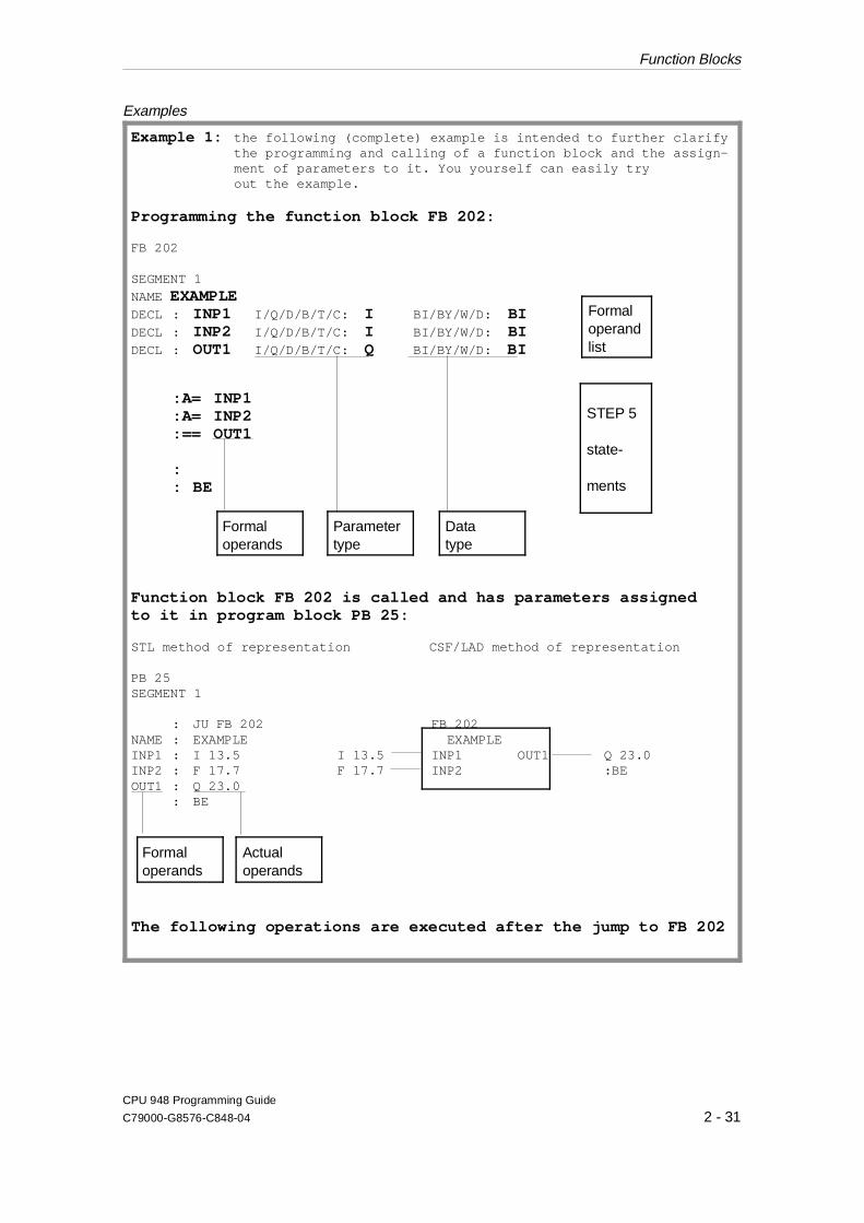
Examples
Example 1: the following (complete) example is intended to further clarifythe programming and calling of a function block and the assign-ment of parameters to it. You yourself can easily tryout the example.
Programming the function block FB 202:
FB 202
SEGMENT 1
NAME EXAMPLEDECL : INP1 I/Q/D/B/T/C: I BI/BY/W/D: BIDECL : INP2 I/Q/D/B/T/C: I BI/BY/W/D: BIDECL : OUT1 I/Q/D/B/T/C: Q BI/BY/W/D: BI
:A= INP1:A= INP2:== OUT1
:: BE
Function block FB 202 is called and has parameters assignedto it in program block PB 25:
STL method of representation CSF/LAD method of representation
PB 25SEGMENT 1
: JU FB 202 FB 202NAME : EXAMPLE EXAMPLEINP1 : I 13.5 I 13.5 INP1 OUT1 Q 23.0INP2 : F 17.7 F 17.7 INP2 :BEOUT1 : Q 23.0
: BE
The following operations are executed after the jump to FB 202
Formaloperandlist
STEP 5
state-
ments
Formaloperands
Parametertype
Datatype
Formaloperands
Actualoperands
Function Blocks
CPU 948 Programming Guide
C79000-G8576-C848-04 2 - 31
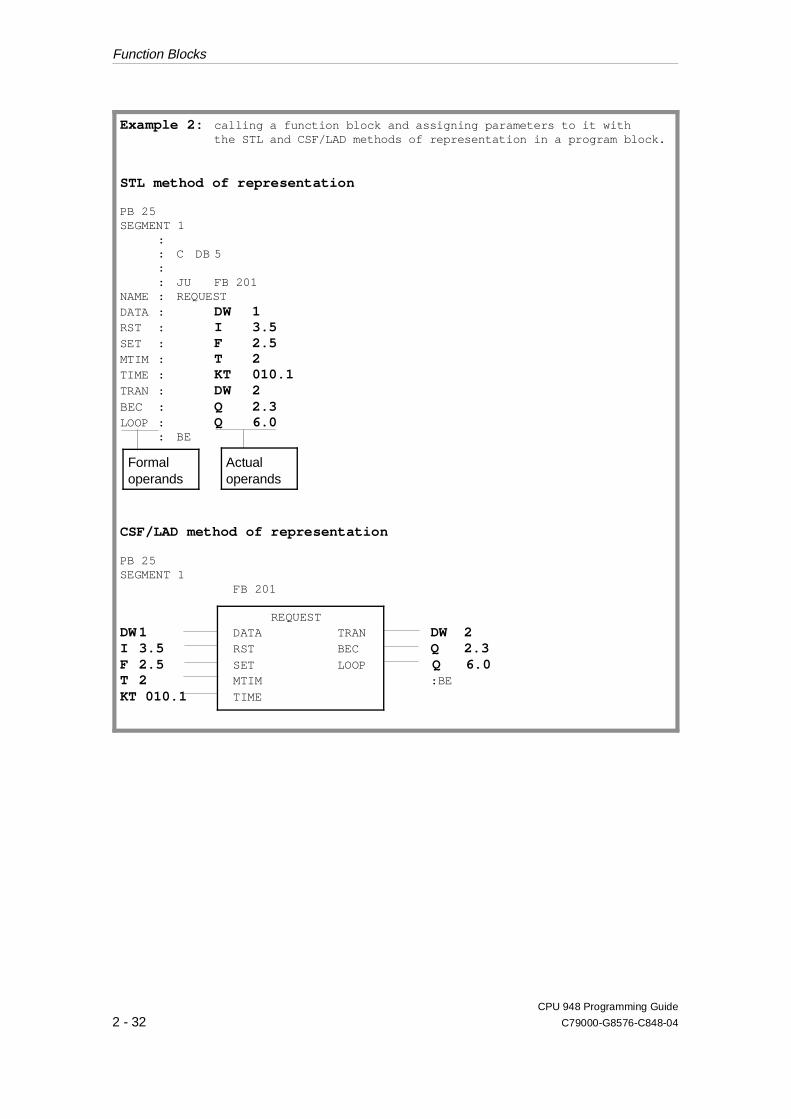
Example 2: calling a function block and assigning parameters to it withthe STL and CSF/LAD methods of representation in a program block.
STL method of representation
PB 25SEGMENT 1
:: C DB 5:: JU FB 201
NAME : REQUESTDATA : DW 1RST : I 3.5SET : F 2.5MTIM : T 2TIME : KT 010.1TRAN : DW 2BEC : Q 2.3LOOP : Q 6.0
: BE
CSF/LAD method of representation
PB 25SEGMENT 1
FB 201
REQUESTDW 1 DATA TRAN DW 2I 3.5 RST BEC Q 2.3F 2.5 SET LOOP Q 6.0T 2 MTIM :BE
KT 010.1 TIME
Formaloperands
Actualoperands
Function Blocks
CPU 948 Programming Guide
2 - 32 C79000-G8576-C848-04
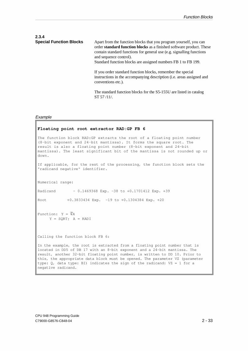
2.3.4Special Function Blocks Apart from the function blocks that you program yourself, you can
order standard function blocks as a finished software product. Thesecontain standard functions for general use (e.g. signalling functionsand sequence control).Standard function blocks are assigned numbers FB 1 to FB 199.
If you order standard function blocks, remember the specialinstructions in the accompanying description (i.e. areas assigned andconventions etc.).
The standard function blocks for the S5-155U are listed in catalog ST 57 /11/.
Example
Floating point root extractor RAD:GP FB 6
The function block RAD:GP extracts the root of a floating point number(8-bit exponent and 24-bit mantissa). It forms the square root. Theresult is also a floating point number (8-bit exponent and 24-bitmantissa). The least significant bit of the mantissa is not rounded up ordown.
If applicable, for the rest of the processing, the function block sets the"radicand negative" identifier.
Numerical range:
Radicand - 0.1469368 Exp. -38 to +0.1701412 Exp. +39
Root +0.3833434 Exp. -19 to +0.1304384 Exp. +20
Function: Y = √AY = SQRT; A = RADI
Calling the function block FB 6:
In the example, the root is extracted from a floating point number that islocated in DD5 of DB 17 with an 8-bit exponent and a 24-bit mantissa. Theresult, another 32-bit floating point number, is written to DD 10. Prior tothis, the appropriate data block must be opened. The parameter VZ (parametertype: Q, data type: BI) indicates the sign of the radicand: VZ = 1 for anegative radicand.
Function Blocks
CPU 948 Programming Guide
C79000-G8576-C848-04 2 - 33
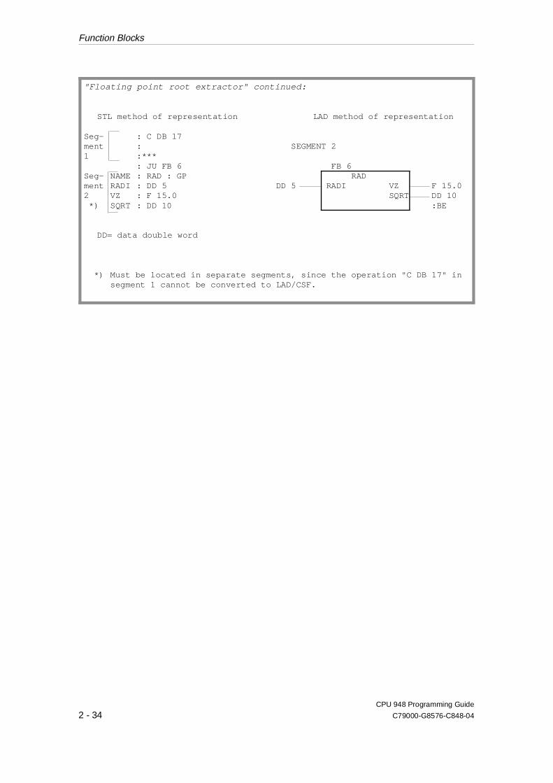
"Floating point root extractor" continued:
STL method of representation LAD method of representation
Seg- : C DB 17ment : SEGMENT 21 :***
: JU FB 6 FB 6Seg- NAME : RAD : GP RADment RADI : DD 5 DD 5 RADI VZ F 15.02 VZ : F 15.0 SQRT DD 10 *) SQRT : DD 10 :BE
DD= data double word
*) Must be located in separate segments, since the operation "C DB 17" insegment 1 cannot be converted to LAD/CSF.
Function Blocks
CPU 948 Programming Guide
2 - 34 C79000-G8576-C848-04
2.4 Data Blocks
Data blocks (DB) or extended data blocks (DX) are used to store thefixed or variable data with which the user program works. No STEP 5operations are processed in data blocks.
The data of a data block includes the following:
•• various bit patterns (e.g. for status of a controlled process)
•• numbers (hexadecimal, binary, decimal) for timer values or arith-metic results
•• alphanumeric characters, e.g. for message texts.
Structure of a data block A data block (DB/DX) consists of the following parts:
•• block preheader (DV, DXV),
•• block header
•• block body.
Block preheader The block preheader is created automatically on the hard or floppydisk of the PG and not transferred to the CPU. It contains the dataformats of the data words entered in the block body. You have noinfluence over the creation of the block preheader.
NoteWhen you transfer a data block from the PLC to diskette or harddisk, the corresponding block preheader can be deleted. For thisreason, you must never modify a data block with different dataformats in the PLC and then transfer it back to diskette, otherwiseall the data words in the DB are automatically assigned the dataformat you selected in the presets screen form.
Data Blocks
CPU 948 Programming Guide
C79000-G8576-C848-04 2 - 35
Block header The block header occupies five words in the memory and containsthe following:
•• the block identifier
•• the programmer identifier
•• the block type and the block number
•• the library number
•• the block length (including the length of the block header).
Block body The block body contains the data words with which the user programworks. These data words are in ascending order in the block body,starting with data word DW 0. Each data word occupies one word(16 bits) in the memory.
Maximum length A data block can occupy a total of maximum 32 767 words (includingheader) in the CPU memory. When you use your programmer to enterand transfer data blocks, remember the size of your CPU memory!
Data Blocks
CPU 948 Programming Guide
2 - 36 C79000-G8576-C848-04
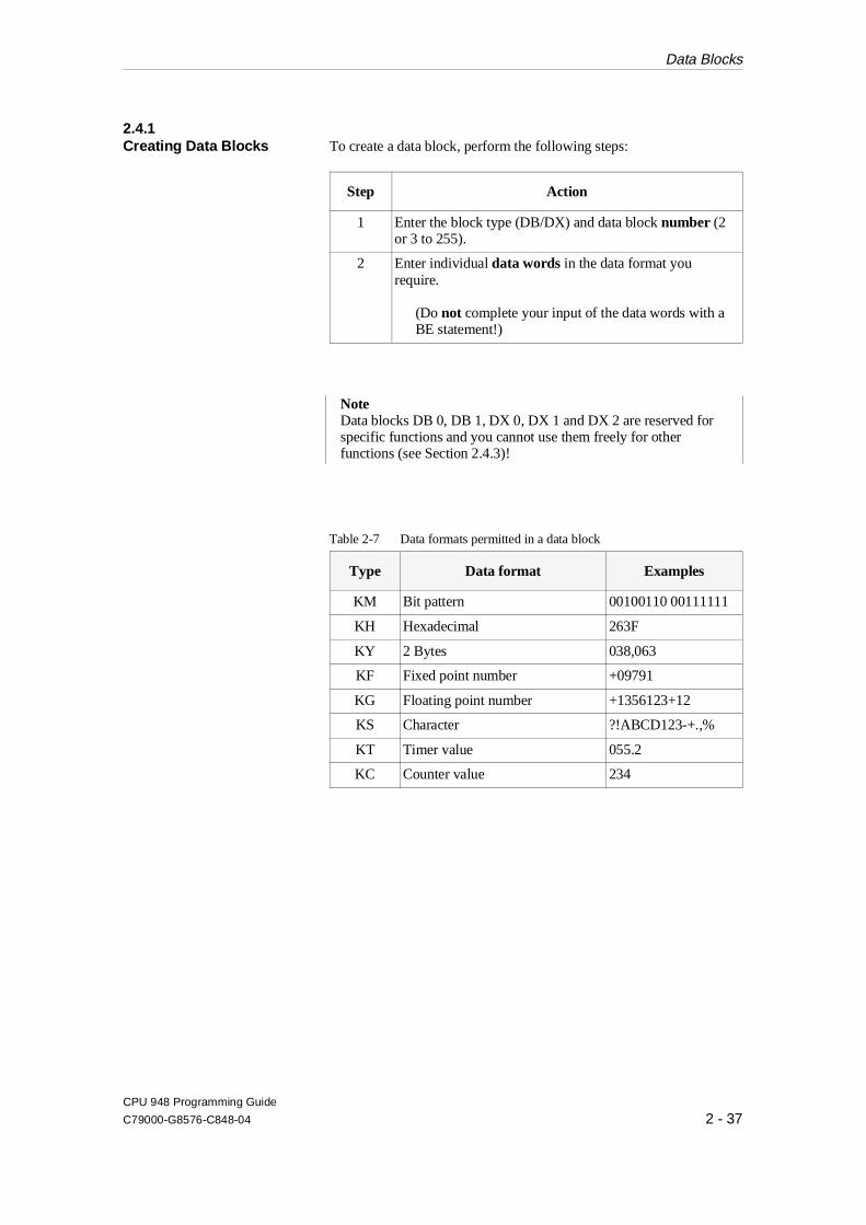
2.4.1Creating Data Blocks To create a data block, perform the following steps:
Step Action
1 Enter the block type (DB/DX) and data block number (2or 3 to 255).
2 Enter individual data words in the data format yourequire.
(Do not complete your input of the data words with aBE statement!)
NoteData blocks DB 0, DB 1, DX 0, DX 1 and DX 2 are reserved forspecific functions and you cannot use them freely for otherfunctions (see Section 2.4.3)!
Type Data format Examples
KM Bit pattern 00100110 00111111
KH Hexadecimal 263F
KY 2 Bytes 038,063
KF Fixed point number +09791
KG Floating point number +1356123+12
KS Character ?!ABCD123-+.,%
KT Timer value 055.2
KC Counter value 234
Table 2-7 Data formats permitted in a data block
Data Blocks
CPU 948 Programming Guide
C79000-G8576-C848-04 2 - 37
2.4.2Opening Data Blocks You can only open a data block (DB/DX) unconditionally. This is
possible within an organization, program, sequence or function block.You can open a specific data block more than once in a program.
To open a data block, perform the following steps:
IF... THEN...
You want to open a DB data block Type in the STEP 5 operation"C DB.."
You want to open a DX datablock
Type in the STEP 5 operation"CX DX."
Validity of a data block After you open a data block, all statements that follow with theoperand area ’D’ refer to the opened data block.
The opened data block also remains valid when the program iscontinued in a different block following a block call.
If a second data block is opened in this new block, the second datablock is only valid in the newly called block from the point at which itis called. After program execution returns to the calling block, the olddata block is once again valid.
Access You can access the data stored in the opened data block duringprogram execution using binary logic operations, set/resetoperations, load or transfer operations (refer to Chapter 3 for moredetailed information).
With a binary operation, the addressed data word bit is used to formthe RLO. The content of the data word is not changed.
With a set/reset operation, the addressed data word bit is assigned thevalue of the RLO. The content of the data word may be changed.
A load operation transfers the contents of the referenced data wordinto ACCU 1. The contents of a data word are not changed.
A transfer operation transfers data from ACCU 1 to the referenceddata word. The old contents of the data word are overwritten.
Data Blocks
CPU 948 Programming Guide
2 - 38 C79000-G8576-C848-04
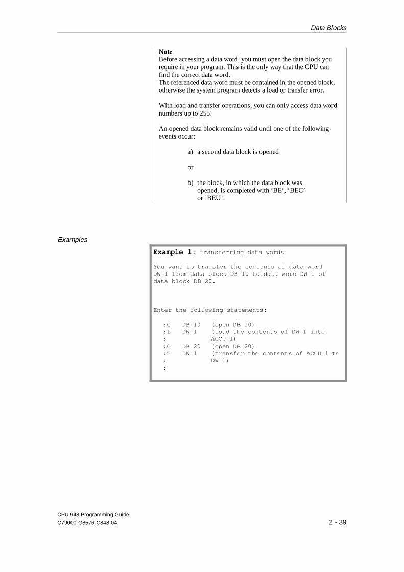
NoteBefore accessing a data word, you must open the data block yourequire in your program. This is the only way that the CPU canfind the correct data word. The referenced data word must be contained in the opened block,otherwise the system program detects a load or transfer error.
With load and transfer operations, you can only access data wordnumbers up to 255!
An opened data block remains valid until one of the followingevents occur:
a) a second data block is opened
or
b) the block, in which the data block wasopened, is completed with ’BE’, ’BEC’ or ’BEU’.
Examples
Example 1: transferring data words
You want to transfer the contents of data wordDW 1 from data block DB 10 to data word DW 1 ofdata block DB 20.
Enter the following statements:
:C DB 10 (open DB 10):L DW 1 (load the contents of DW 1 into : ACCU 1):C DB 20 (open DB 20):T DW 1 (transfer the contents of ACCU 1 to: DW 1) :
Data Blocks
CPU 948 Programming Guide
C79000-G8576-C848-04 2 - 39

Example 2: range of validity of data blocks (Fig. 2-5)
Data block DB 10 is opened in program block PB 7 (C DB 10). During thesubsequent program execution, the data of this data block are processed.
After the call (JU PB 20) program block PB 20 is processed. Data blockDB 10, however, remains valid. The data area only changes when data blockDB 11 (C DB 11) is opened.Data block DB 11 now remains valid until the end of program block PB 20(BE).
After the jump back to program block PB 7, data block DB 10 is once againvalid.
PB 7
C DB 11
BE
PB 20
C DB 10
JU PB 20
BE
Range of val idi ty of DB 10
Range of val idi ty of DB 11
Fig. 2-5 Range of validity of an opened data block
Data Blocks
CPU 948 Programming Guide
2 - 40 C79000-G8576-C848-04

2.4.3Special Data Blocks On the CPU 948 data blocks DB 0, DB 1, DX 0, DX 1 and DX 2 are
reserved for special functions. They are managed by the systemprogram and you cannot use them freely for other functions.
DB 0 •• Data block DB 0 (see Section 8.3.2)
Data block DB 0 contains the address list with the start addressesof all blocks that are located in the data block RAM of the CPU.The system program generates this address list during initialization(following each POWER UP or OVERALL RESET) and it is up-dated automatically when you use a programmer to change datablocks or generate a new data block.
DB 1 •• Data block DB 1 (see Section 10.1.6)
Data block DB 1 contains the list of digital inputs/outputs (P periphe-ral with relative byte addresses from 0 to 127) and the interprocessorcommunication (IPC) flag inputs and outputs that are assigned to theCPU. If applicable, the block may also contain a timer field length.
DB 1 can have parameters assigned and be loaded as follows:to reduce the cycle time in single processor operation, since only the inputs, outputs or timers entered in DB1 are updated.
DB 1 must be assigned parameters and loaded as follows:a) for multiprocessingb) when IPC flags exist with CPs
DX 0 •• Data block DX 0 (see Chapter 7)
If you assign parameters to data block DX 0 and load it, you can chan-ge the defaults of certain system program functions (e.g. the start-upprocedure) and adapt the performance of the system program to yourparticular application.
DX 1 •• Data block DX 1
Reserved.
DX 2 •• Data block DX 2
Reserved for the second serial interface.
Data Blocks
CPU 948 Programming Guide
C79000-G8576-C848-04 2 - 41

Data Blocks
CPU 948 Programming Guide
2 - 42 C79000-G8576-C848-04
Contents of Chapter 3
3.1 Principle of Program Execution . . . . . . . . . . . . . . . . . . . . . . . . . . . . . . . . . . . . . . . . . . . . . 3 - 4
3.2 Program Organization. . . . . . . . . . . . . . . . . . . . . . . . . . . . . . . . . . . . . . . . . . . . . . . . . . . . . 3 - 5
3.3 Storing Program and Data Blocks . . . . . . . . . . . . . . . . . . . . . . . . . . . . . . . . . . . . . . . . . . 3 - 10
3.4 Processing the User Program . . . . . . . . . . . . . . . . . . . . . . . . . . . . . . . . . . . . . . . . . . . . . . 3 - 11
3.4.1 Definition of Terms used in Program Execution. . . . . . . . . . . . . . . . . . . . . . . . . . . . . . . 3 - 12
3.5 STEP 5 Operations with Examples . . . . . . . . . . . . . . . . . . . . . . . . . . . . . . . . . . . . . . . . . 3 - 15
3.5.1 Basic Operations . . . . . . . . . . . . . . . . . . . . . . . . . . . . . . . . . . . . . . . . . . . . . . . . . . . . . . . . 3 - 193.5.2 Programming Examples in the STL, LAD and CSF Methods of Representation . . . . . 3 - 343.5.3 Supplementary Operations . . . . . . . . . . . . . . . . . . . . . . . . . . . . . . . . . . . . . . . . . . . . . . . . 3 - 493.5.4 Executive Operations . . . . . . . . . . . . . . . . . . . . . . . . . . . . . . . . . . . . . . . . . . . . . . . . . . . . 3 - 593.5.5 Semaphore Operations . . . . . . . . . . . . . . . . . . . . . . . . . . . . . . . . . . . . . . . . . . . . . . . . . . . 3 - 75
3Program Execution
CPU 948 Programming Guide
C79000-G8576-C848-04 3 - 1

Contents
CPU 948 Programming Guide
3 - 2 C79000-G8576-C848-04

3Program Execution
This chapter is intended for readers who do not yet have any greatexperience in using the programming language. The chapter thereforedeals with the basics of STEP 5 programming and explains in detail(with examples) the STEP 5 operations for the CPU 948.
Experienced readers who require more information about a specificSTEP 5 operation listed in the Pocket Guide can refer to the referencesection in 3.5.
CPU 948 Programming Guide
C79000-G8576-C848-04 3 - 3

3.1 Principle of Program Execution
You can process your STEP 5 user program in various ways.
Cyclic program execution is most common with programmablecontrollers (PLCs). The system program runs through a program loop(the cycle, refer to Section 3.4) and calls organization block OB 1cyclically in each loop (refer to Fig. 3-1).
Cal l OB1 BE
Cal l PB 20
BE
PB 20
OB 1
Update inter-processor comm.f lag outputs
image outputs(PIQ)
Update process
Tr igger cycle t ime
Update inter-processor comm.f lag inputs
image inputs(PI I )
Update process
from start -up
System program User program
Fig. 3-1 Principle of cyclic program execution
Principle of Program Execution
CPU 948 Programming Guide
3 - 4 C79000-G8576-C848-04
3.2 Program Organization
Program organization allows you to specify which conditions affect theprocessing of your blocks and the order in which they are processed.Organize your program by programming organization blocks withconditional or unconditional calls for the blocks you require.
You can call additional program, function and sequence blocks in anycombination in the program of individual organization, program,function and sequence blocks. You can call these one after another ornested in one another.
For maximum efficiency, you should organize your program toemphasise the most important program structures and in such a waythat you can clearly recognize parts of the controlled system which arerelated in the software.
Figs. 3-2 and 3-3 are examples of a program structure.
Program Organization
CPU 948 Programming Guide
C79000-G8576-C848-04 3 - 5

PB ‘B‘
OB 1 PB ’A’ FB
FB
Go to in i t ia ls tate
Stop to the systemEMERGENCYOFF
PB ‘D‘
Message output
FB
Message outputv ia standardper ipherals
FB
Message outputv ia standardper ipherals
DXMessagetexts
PB ‘C‘
Indiv idualcontro l level
FB
Groupin i t ia l izat ion
DB
Inter face f lagsof the indiv idualcontro le lementsFX
Indiv idualin i t ia l izat ion
FX
Indiv idualin i t ia l izat ion
Sequencecontro l
Contro l ofsequencecascade
FB SB
Sequencestep
SB
Sequencestep
JU PB ’A’
JU PB ‘B‘
JU PB ‘C‘
JU PB ‘D‘
BE
Operat ing modeprogram
Fig. 3-2 Example of the organization of the user program according to the program structure
Program Organization
CPU 948 Programming Guide
3 - 6 C79000-G8576-C848-04
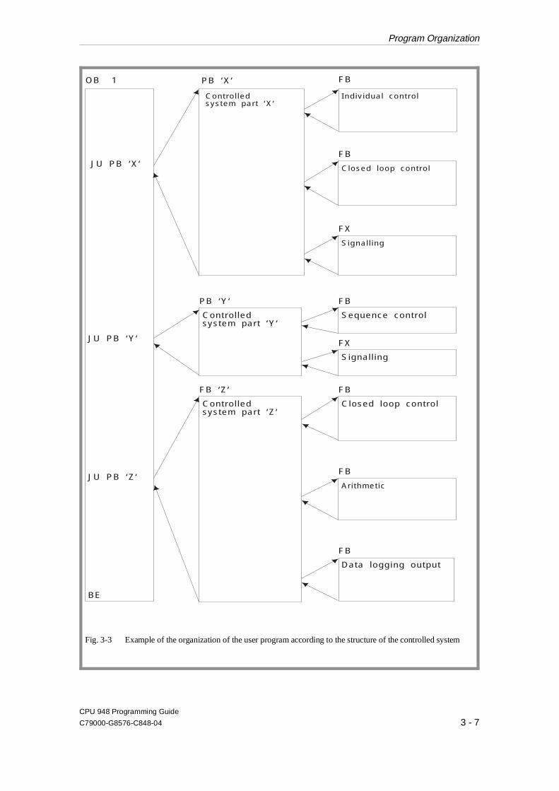
OB 1
JU PB ‘X‘
JU PB ‘Y‘
BE
Control ledsystem part ‘Z‘
PB ‘X‘
Contro l ledsystem part ‘X‘
FB
Indiv idual contro l
FB
Closed loop contro l
FX
Signal l ing
Control ledsystem part ‘Y‘
PB ‘Y‘ FB
Sequence control
FX
Signal l ing
FB
Closed loop control
FB
Ari thmet icJU PB ‘Z‘
FB
Data logging output
FB ‘Z‘
Fig. 3-3 Example of the organization of the user program according to the structure of the controlled system
Program Organization
CPU 948 Programming Guide
C79000-G8576-C848-04 3 - 7
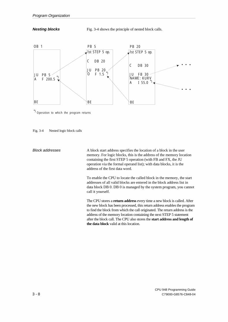
Nesting blocks Fig. 3-4 shows the principle of nested block calls.
Block addresses A block start address specifies the location of a block in the usermemory. For logic blocks, this is the address of the memory locationcontaining the first STEP 5 operation (with FB and FX, the JUoperation via the formal operand list); with data blocks, it is theaddress of the first data word.
To enable the CPU to locate the called block in the memory, the startaddresses of all valid blocks are entered in the block address list indata block DB 0. DB 0 is managed by the system program, you cannotcall it yourself.
The CPU stores a return address every time a new block is called. Afterthe new block has been processed, this return address enables the programto find the block from which the call originated. The return address is theaddress of the memory location containing the next STEP 5 statementafter the block call. The CPU also stores the start address and length ofthe data block valid at this location.
OB 1
BE
PB 20
BE
PB 5
CC
DB 20DB 30
BE
JU PB 5F 200.5
*)
JUJU
PB 20FB 30O F 1.5 *)
NAME: KURVA I 55.0 *)
*) Operat ion to which the program returns
A
1st STEP 5 op. 1st STEP 5 op.
Fig. 3-4 Nested logic block calls
Program Organization
CPU 948 Programming Guide
3 - 8 C79000-G8576-C848-04
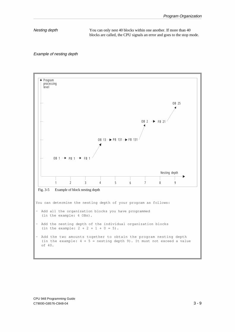
Nesting depth You can only nest 40 blocks within one another. If more than 40blocks are called, the CPU signals an error and goes to the stop mode.
Example of nesting depth
You can determine the nesting depth of your program as follows:
- Add all the organization blocks you have programmed (in the example: 4 OBs).
- Add the nesting depth of the individual organization blocks(in the example: 2 + 2 + 1 + 0 = 5).
- Add the two amounts together to obtain the program nesting depth (in the example: 4 + 5 = nesting depth 9). It must not exceed a valueof 40.
OB 25
Nesting depth
1 2 3 4 5 6 7 8 9
OB 1 PB 1 FB 1
OB 13 PB 131 FB 131
OB 2 FB 21
Programprocessinglevel
Fig. 3-5 Example of block nesting depth
Program Organization
CPU 948 Programming Guide
C79000-G8576-C848-04 3 - 9
3.3 Storing Program and Data Blocks
On the CPU 948, the user program runs solely in the internal RAM.The user program including data blocks must, therefore, be loaded inthe CPU 948 user memory.
How do I load programs anddata blocks in the internalRAM?
You can use the following methods:
•• You can load the individual logic and data blocks in the RAMusing your PG.
•• You can program a memory card (flash EPROM!) with yourcomplete program including data blocks on the PG and then insertthe card in the receptacle on the CPU. If you do an overall reset on the CPU (refer to Chapter 4) thecomplete contents of the memory card are loaded "1:1" in theinternal RAM.
•• You loaded your program in the internal RAM with the PG orfrom the memory card with an OVERALL RESET. You can thenload additional blocks with the PG or replace existing blocks.
NoteYou can only program the memory card on the PG. Use the PGsoftware from version 6 upwards. When programming, the PG mustbe in the mode "WORD FIELD" (refer to the STEP 5 manual /3/).
CautionIf you have changed or added blocks using the PG after loadingyour program from the memory card, these changes are reversedby the next OVERALL RESET , since the memory isoverwritten again with the contents of the memory card.
Storing Program and Data Blocks
CPU 948 Programming Guide
3 - 10 C79000-G8576-C848-04
3.4 Processing the User Program
The complete software on the CPU (consisting of the system programand the STEP 5 user program) has the following tasks:
•• CPU START-UP
•• Controlling an automation process by continuously repeatingoperations (CYCLE).
•• Controlling an automation process by reacting to events occurringsporadically or at certain times (interrupts) and reacting to errors.
For all three tasks, you can select special parts of your program to runon the CPU by programming user interfaces (organization blocks OB 1 to OB 35 - refer to Section 2.2.3).
START-UP Before the CPU can start cyclic program execution, an initializationmust be performed to establish a defined initial status for cyclicprogram execution and, for example, to specify a time base for theexecution of certain functions. The way in which this initialization isperformed depends on the event that led to a START-UP and onsettings that you can make on your CPU. For more detailedinformation, refer to Chapter 4.
You can influence the START-UP procedure of your CPU byprogramming organization blocks OB 20, OB 21 and OB 22 or byassigning parameters in DX 0 (refer to Chapter 7).
CYCLE Following the START-UP, the system program goes over to cyclicprocessing. It is responsible for background functions required for theautomation tasks (refer to Fig. 3-1 at the beginning of this section).After the system functions have been executed at the beginning of aCYCLE, the system program calls organization block OB 1 orfunction block FB 0 as the cyclic user program. You program theSTEP 5 operations for cyclic processing in this block.
Processing the User Program
CPU 948 Programming Guide
C79000-G8576-C848-04 3 - 11
Reactions to interrupts and errors
To allow you to specify the reactions to interrupts or errors, specialorganization blocks (OB 2 to OB 18 for interrupt servicing, OB 19and OB 23 to OB 34 for reactions to errors) are available on theCPU 948. You can store an appropriate STEP 5 program in these blocks.
When interrupts or errors are to be processed, the system programactivates the corresponding organization block during cyclicprocessing. This means that the cyclic processing is interrupted toservice an interrupt or to react to an error. The nesting of theorganization blocks has a fixed priority (for further information, referto Chapters 4 and 5).
In addition to the organization blocks, you can also influence thereaction of the CPU to interrupt servicing by assigning parameters indata block DX 0.
Organization blocks OB 1 to OB 39 can be called by the systemprogram as soon as they are loaded in the program memory (alsoduring operation).If the OBs are not loaded, there is either no reaction from the CPU or(in the event of errors) it goes to the stop mode (refer also to Section5.4).
You can also load data block DX 0 into the program memory duringoperation like the organization blocks. It is, however, only effectiveafter the next COLD RESTART. If DX 0 is not loaded, the standardsettings apply (refer to Chapter 7).
3.4.1Definition of Terms used inProgram Execution
Cycle time The cycle begins when the cycle monitoring time is triggered and endswith the next trigger. The time that the CPU requires to execute theprogram between two triggers is called the cycle time. The cycle timeconsists of the runtime of the system program and the runtime of theuser program.
The cycle time therefore includes the following:
•• the time required to process the cyclic program (system and userprogram),
•• the time required to process interrupts (e.g. time-controlledinterrupt),
•• the time required to process interruptions (errors).
Processing the User Program
CPU 948 Programming Guide
3 - 12 C79000-G8576-C848-04
Cycle time monitoring The CPU monitors the cycle time in case it exceeds a maximum value.The standard setting for this maximum value is 200 ms. You can set thecycle time monitoring yourself or restart it during user program execution(refer to DX 0/Chapter 7 and special function OB OB 222/Section 6.16).
Process input and outputimage (PII and PIQ)
The process image of the inputs and outputs is a memory area in theinternal RAM.Before cyclic execution of the user program begins, the systemprogram reads the signal states of the input peripheral modules andtransfers them to the process input image. The user program evaluatesthe signal states in the process input image and then sets theappropriate signal states for the outputs in the process output image.After the user program has been processed, the system programtransfers the signal states of the process output image to the outputperipheral modules.
Buffering the I/O signals in the process image of the inputs andoutputs avoids a change in a bit within a program cycle from causingthe corresponding output to "flutter".
The process image is therefore a memory area whose contents areoutput to the peripherals and read in from the peripherals once percycle.
NoteThe process image only exists for input and output bytes of the "P"peripherals with byte addresses from 0 to 127!Apart from the process image integrated in the system, you can useOB 126 to define and transfer further process images (refer toSection 6.6)
Interprocessor communication(IPC) flags
IPC flags exchange data between individual CPUs (multiprocessing) orbetween the CPU and some communication processors.
The system program reads the input IPC flags of the CPU before cyclicexecution of the user program begins. After the STEP 5 program isprocessed, the system program transfers the output IPC flags to thecoordinator or to the communications processors.
You define the input and output IPC flags when you create data blockDB 1 (refer to Section 10.1.6).
Processing the User Program
CPU 948 Programming Guide
C79000-G8576-C848-04 3 - 13
Interrupt events Cyclic program execution can be interrupted by the following:
•• time-controlled program execution (delayed interrupt, cyclic timedinterrupts, clock-controlled interrupts),
•• interrupt-driven program execution (process interrupt, systeminterrupt).
The cyclic program can be interrupted or even aborted completely bythe following:
•• a device hardware fault or program error
•• operator intervention (using the PC stop function, or setting themode selector to "stop", multiprocessor stop MP-STP),
•• a stop operation
Processing the User Program
CPU 948 Programming Guide
3 - 14 C79000-G8576-C848-04

3.5 STEP 5 Operations with Examples
A STEP 5 operation consists of the operation and an operand. Theoperation specifies what the CPU is to do (operation). The operandspecifies with what an operation is to be executed.
STEP 5 operations can be divided into the following groups:
•• basic operations (can be used in all logic blocks),
•• supplementary operations,
•• executive operations (can only be used in FB/FX function blocks),
•• semaphore operations (can only be used in FB/FX function blocks).
Accumulators as workingregisters
The CPU 948 has four accumulators, ACCU 1 to ACCU 4. MostSTEP 5 operations use two 32-bit registers (ACCU 1 and ACCU 2) asthe source of operands and the destination for results.
The STEP 5 operation to be carried out affects the accumulators, e.g.:
•• ACCU 1 is always the destination in load operations. A loadoperation shifts the old contents of ACCU 1 to ACCU 2 (stacklift). Accumulators 3 and 4 are not changed by any load operations.
1) analogous for ACCU 2 to ACCU 4
ACCU-1-H
High byte Low byte High byte Low byteACCU 1 1)
High word Low word
31 24 23 16 15 8 7 0
ACCU-1-HL ACCU-1-LH ACCU-1-LL
ACCU-1-L
ACCU-1-HH
STEP 5 Operations with Examples
CPU 948 Programming Guide
C79000-G8576-C848-04 3 - 15
•• Arithmetic operations combine the contents of ACCU 1 with thoseof ACCU 2, write the result to ACCU 1 and transfer the contentsof ACCU 3 to ACCU 2 and the contents of ACCU 4 to ACCU 3(stack drop). In 16-bit fixed point arithmetic, only the low word orACCU 3 is transferred to the low word of ACCU 2 and the lowword of ACCU 4 to the low word of ACCU 3.
•• When a constant is added (ADD BF/KF/DH) to the contents ofACCU 1, the accumulators 2, 3 and 4 are not changed.
Condition codes STEP 5 operations either set or evaluate condition codes. The conditioncodes are written to a condition code byte. Two groups of condition codescan be distinguished: condition codes of digital operations (wordcondition codes - bits 4 to 7 in the condition code byte) and conditioncodes from binary and executive operations (bit condition codes - bits 0 to3 in the condition code byte). You can see how the various conditioncodes are influenced or evaluated by STEP 5 operations be referring tothe operation list /1/.
You can display the condition code byte on a programmer using the"STATUS" online function (refer to Section 11.2.3). The byte has thefollowing structure:
Word condition codes Bit condition codes
CC 1 CC 0 OV OS OR STA RLO ERABBit 7 6 5 4 3 2 1 0
Bit condition codes •• ERAB First bit scan
A logic operation sequence containing binary operations alwaysbegins with the first bit scan, following which a new RLO isformed. The bit condition code ERAB = 1 is then set. While theremaining logic operations in the sequence are being performed,ERAB remains set to 1 and the RLO cannot be changed by theselogic operations.
The active sequence of logic operations is terminated by a binaryset/reset operation (e.g. S Q 5.0). The set/reset operation setsERAB to 0; the RLO can be evaluated (e.g. by RLO-dependentoperations) but can no longer be combined logically. The nextbinary logic operation following a binary set/reset operation isonce again a first bit scan.
STEP 5 Operations with Examples
CPU 948 Programming Guide
3 - 16 C79000-G8576-C848-04

Example of ERAB
Other bit condition codes •• RLO Result of logic operation
This is the result of bit logic operations. It is the truth statement forcomparison operations (refer to operations list, binary logicoperations or comparison operations).
•• STA Status
For bit operations, this indicates the logical status of the bit justscanned or set. The status is updated in binary logic operations -except for A(, O(,), O and for set/reset operations.
•• OR Or
Internal CPU bit for handling "AND before OR" logic operations.
Word condition codes •• OV Overflow
This indicates whether the permissible number range was exceededduring the arithmetic operation just completed.
•• OS Stored overflow
The overflow bit is stored. It can be used in several arithmeticoperations to indicate whether an overflow occurred at any pointduring the operations.
:A I 1.0 ERAB is set to ’1’, : the new RLO is formed by: an AND operation:O I 6.3 The RLO is influenced by : an OR operation:AN I 2.1 The RLO is influenced by: an AND NOT operation.:S Q 2.4 ERAB is set to ’0’, : the sequence is now complete:JC FB 150 The function block is called: dependent on the RLO.::
STEP 5 Operations with Examples
CPU 948 Programming Guide
C79000-G8576-C848-04 3 - 17
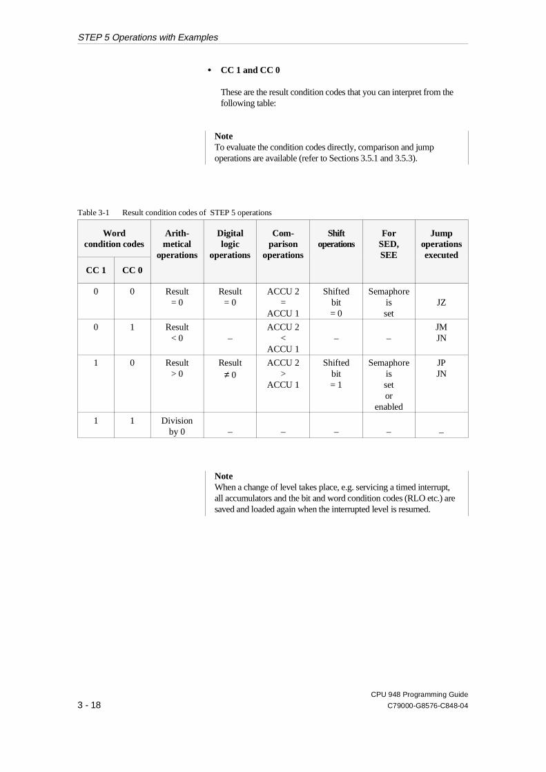
•• CC 1 and CC 0
These are the result condition codes that you can interpret from thefollowing table:
NoteTo evaluate the condition codes directly, comparison and jumpoperations are available (refer to Sections 3.5.1 and 3.5.3).
Wordcondition codes
Arith-metical
operations
Digitallogic
operations
Com-parison
operations
Shiftoperations
ForSED,SEE
Jumpoperationsexecuted
CC 1 CC 0
0 0 Result= 0
Result= 0
ACCU 2=
ACCU 1
Shiftedbit= 0
Semaphoreisset
JZ
0 1 Result< 0 –
ACCU 2<
ACCU 1– –
JMJN
1 0 Result> 0
Result≠ 0
ACCU 2>
ACCU 1
Shiftedbit= 1
Semaphoreissetor
enabled
JPJN
1 1 Divisionby 0 – – – – –
NoteWhen a change of level takes place, e.g. servicing a timed interrupt,all accumulators and the bit and word condition codes (RLO etc.) aresaved and loaded again when the interrupted level is resumed.
Table 3-1 Result condition codes of STEP 5 operations
STEP 5 Operations with Examples
CPU 948 Programming Guide
3 - 18 C79000-G8576-C848-04
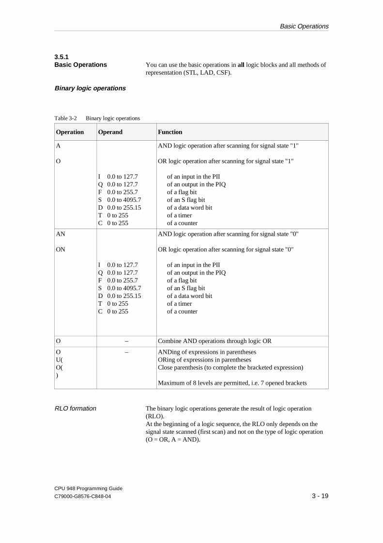
3.5.1Basic Operations You can use the basic operations in all logic blocks and all methods of
representation (STL, LAD, CSF).
Binary logic operations
Operation Operand Function
A
O
I 0.0 to 127.7Q 0.0 to 127.7F 0.0 to 255.7S 0.0 to 4095.7D 0.0 to 255.15T 0 to 255C 0 to 255
AND logic operation after scanning for signal state "1"
OR logic operation after scanning for signal state "1"
of an input in the PIIof an output in the PIQof a flag bitof an S flag bitof a data word bitof a timerof a counter
AN
ON
I 0.0 to 127.7Q 0.0 to 127.7F 0.0 to 255.7S 0.0 to 4095.7D 0.0 to 255.15T 0 to 255C 0 to 255
AND logic operation after scanning for signal state "0"
OR logic operation after scanning for signal state "0"
of an input in the PIIof an output in the PIQof a flag bitof an S flag bitof a data word bitof a timerof a counter
O – Combine AND operations through logic OR
OU(O()
– ANDing of expressions in parenthesesORing of expressions in parentheses Close parenthesis (to complete the bracketed expression)
Maximum of 8 levels are permitted, i.e. 7 opened brackets
RLO formation The binary logic operations generate the result of logic operation(RLO).At the beginning of a logic sequence, the RLO only depends on thesignal state scanned (first scan) and not on the type of logic operation(O = OR, A = AND).
Table 3-2 Binary logic operations
Basic Operations
CPU 948 Programming Guide
C79000-G8576-C848-04 3 - 19
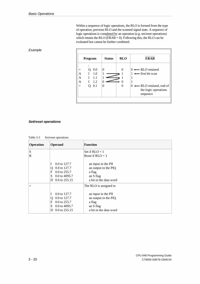
Within a sequence of logic operations, the RLO is formed from the typeof operation, previous RLO and the scanned signal state. A sequence oflogic operations is completed by an operation (e.g. set/reset operations)which retains the RLO (ERAB = 0). Following this, the RLO can beevaluated but cannot be further combined.
Example
Set/reset operations
Operation Operand Function
SR
I 0.0 to 127.7Q 0.0 to 127.7F 0.0 to 255.7S 0.0 to 4095.7D 0.0 to 255.15
Set if RLO = 1Reset if RLO = 1
an input in the PIIan output in the PIQa flagan S flaga bit in the data word
=
I 0.0 to 127.7Q 0.0 to 127.7F 0.0 to 255.7S 0.0 to 4095.7D 0.0 to 255.15
The RLO is assigned to
an input in the PIIan output in the PIQa flagan S flaga bit in the data word
Program Status RLO ERAB
:= Q 0.0A I 1.0A I 1.1A I 1.2= Q 0.1
01100
01100
0 RLO retained1 first bit scan110 RLO retained, end of
the logic operationssequence
Table 3-3 Set/reset operations
Basic Operations
CPU 948 Programming Guide
3 - 20 C79000-G8576-C848-04
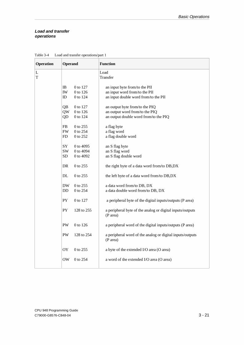
Load and transferoperations
Operation Operand Function
LT
IB 0 to 127IW 0 to 126ID 0 to 124
QB 0 to 127QW 0 to 126QD 0 to 124
FB 0 to 255FW 0 to 254FD 0 to 252
SY 0 to 4095SW 0 to 4094SD 0 to 4092
DR 0 to 255
DL 0 to 255
DW 0 to 255DD 0 to 254
PY 0 to 127
PY 128 to 255
PW 0 to 126
PW 128 to 254
OY 0 to 255
OW 0 to 254
LoadTransfer
an input byte from/to the PIIan input word from/to the PIIan input double word from/to the PII
an output byte from/to the PIQan output word from/to the PIQan output double word from/to the PIQ
a flag bytea flag worda flag double word
an S flag bytean S flag wordan S flag double word
the right byte of a data word from/to DB,DX
the left byte of a data word from/to DB,DX
a data word from/to DB, DXa data double word from/to DB, DX
a peripheral byte of the digital inputs/outputs (P area)
a peripheral byte of the analog or digital inputs/outputs(P area)
a peripheral word of the digital inputs/outputs (P area)
a peripheral word of the analog or digital inputs/outputs(P area)
a byte of the extended I/O area (O area)
a word of the extended I/O area (O area)
Table 3-4 Load and transfer operations/part 1
Basic Operations
CPU 948 Programming Guide
C79000-G8576-C848-04 3 - 21
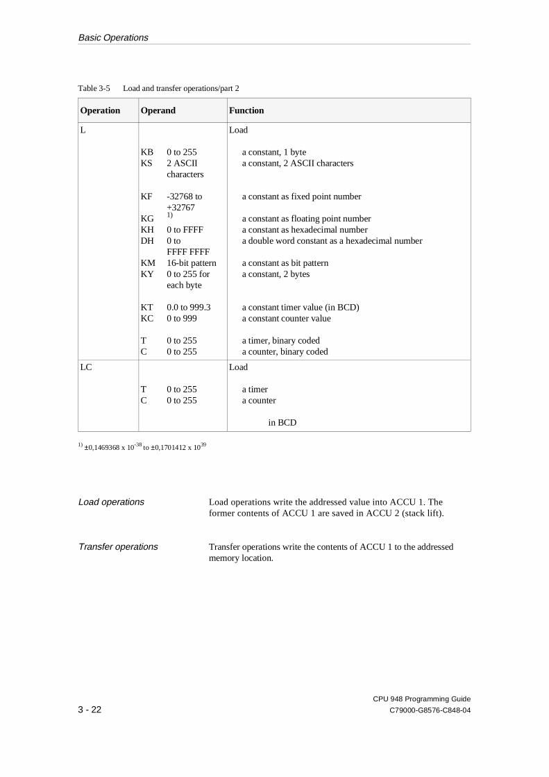
Operation Operand Function
L
KB 0 to 255KS 2 ASCII
characters
KF -32768 to+32767
KG 1)
KH 0 to FFFFDH 0 to
FFFF FFFFKM 16-bit patternKY 0 to 255 for
each byte
KT 0.0 to 999.3KC 0 to 999
T 0 to 255C 0 to 255
Load
a constant, 1 bytea constant, 2 ASCII characters
a constant as fixed point number
a constant as floating point numbera constant as hexadecimal numbera double word constant as a hexadecimal number
a constant as bit patterna constant, 2 bytes
a constant timer value (in BCD)a constant counter value
a timer, binary codeda counter, binary coded
LC
T 0 to 255C 0 to 255
Load
a timera counter
in BCD
1) ±0,1469368 x 10-38 to ±0,1701412 x 1039
Load operations Load operations write the addressed value into ACCU 1. Theformer contents of ACCU 1 are saved in ACCU 2 (stack lift).
Transfer operations Transfer operations write the contents of ACCU 1 to the addressedmemory location.
Table 3-5 Load and transfer operations/part 2
Basic Operations
CPU 948 Programming Guide
3 - 22 C79000-G8576-C848-04
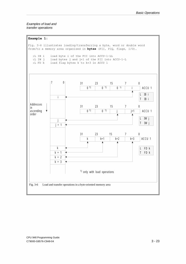
Examples of load andtransfer operations
Example 1:
Fig. 3-6 illustrates loading/transferring a byte, word or double wordfrom/to a memory area organized in bytes (PII, PIQ, flags, I/O).
:L IB i load byte i of the PII into ACCU-1-LL:L IW j load bytes j and j+1 of the PII into ACCU-1-L:L FD k load flag bytes k to k+3 in ACCU 1
ACCU 1
ACCU 1
ACCU 1
jj + 1
i
kk + 1k + 2k + 3
31 23 15 7 0
31 23 15 7 0
31 23 15 7 0k+1 k+2 k+3
0 0 j j+1
0 0 0 i
7 0
Addressesinascendingorder
k
1) 1)
1) 1) 1)
L IB iT IB i
T IW jL IW j
T FD kL FD k
1) only wi th load operat ions
Fig. 3-6 Load and transfer operations in a byte-oriented memory area
Basic Operations
CPU 948 Programming Guide
C79000-G8576-C848-04 3 - 23
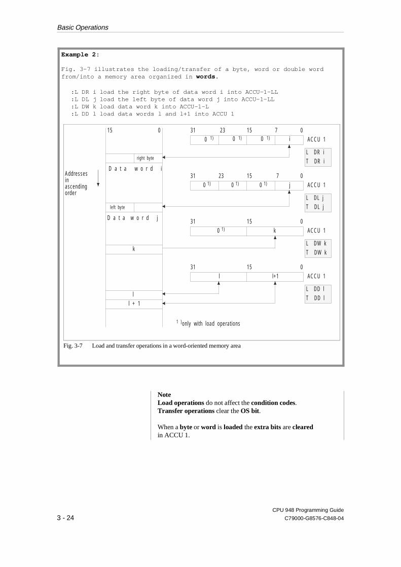
NoteLoad operations do not affect the condition codes. Transfer operations clear the OS bit.
When a byte or word is loaded the extra bits are cleared in ACCU 1.
Example 2:
Fig. 3-7 illustrates the loading/transfer of a byte, word or double wordfrom/into a memory area organized in words .
:L DR i load the right byte of data word i into ACCU-1-LL:L DL j load the left byte of data word j into ACCU-1-LL:L DW k load data word k into ACCU-1-L:L DD l load data words l and l+1 into ACCU 1
ll + 1
k
31 23 15 7 0
31 23 15 7 0
31 15 0
31 15 0
ACCU 1
ACCU 1
ACCU 1
ACCU 1
15 0
l l+1
k
j
0 0 0 i
0 0 0
1) 1) 1)
0
1) 1) 1)
1)
left byte
D a t a w o r d j
L DR iT DR i
L DL jT DL j
L DW kT DW k
L DD lT DD l
right byte
D a t a w o r d iAddressesinascendingorder
1 )only wi th load operat ions
Fig. 3-7 Load and transfer operations in a word-oriented memory area
Basic Operations
CPU 948 Programming Guide
3 - 24 C79000-G8576-C848-04

Addressing I/Os You can use load and transfer operations to address the I/O peripheralsas follows:
•• directly using the following operations:
L../T.. ..PY, ..PW, ..OY, ..OW
or
•• using the process image with the following operations:
L../T.. ..IB, ..IW, ..ID, .QB, ..QW, ..QD
and with logic and set/reset operations
NoteIf you use the transfer operations T PY 0 to 127 and T PW 0 to126, the process output image is updated at the same time.Exception: command output is disabled by the STEP 5 operationBAS (refer to Section 3.5.4).
Note the following points about I/O peripherals:
•• A process input/output image exists for 128 input and 128 outputbytes of the P peripherals with byte addresses from 0 to 127.
•• No process image exists for the entire area of the O peripherals andthe P peripherals with relative byte addresses from 128 to 256.(For more information on address space allocation see Section 8.2.2).
•• I/O modules with addresses of the O peripherals can only be plug-ged into expansion units (not in the central controller).
•• In one expansion unit, you can use either only P peripherals oronly O peripherals.
CautionIf you use relative addresses of the O peripherals in an expansionunit, you can no longer use these addresses for I/O modules in thecentral controller (this would result in double addressing).
Basic Operations
CPU 948 Programming Guide
C79000-G8576-C848-04 3 - 25

Timer and Counteroperations
To load a timer using a start operation or a counter using a setoperation, you must first load the value in ACCU 1.
The following load operations are preferable:
For timers: L KT, L IW, L QW, L FW, L DW, L SW.For counters: L KC, L IW, L QW, L FW, L DW, L SW.
Starting a timer with the selected timer value requires an RLO signalchange.
A counter is set or started with the selected counter value when apositive-going RLO signal edge is detected.
The following table indicates the signal edge change withcorresponding arrows.
Operation Operand RLO1)
Function
SPSESDSSSFR
T 0 to 255T 0 to 255T 0 to 255T 0 to 255T 0 to 255T 0 to 255
↑↑↑↑↓1
Start a timer as a pulseStart a timer as extended pulseStart a timer as ON delayStart a timer as stored ON delayStart a timer as OFF delayReset a timer
SRCUCD
C 0 to 255C 0 to 255C 0 to 255C 0 to 255
↑1↑↑
Set a counter (BCD number from 0 to 999)Reset a counterCount upCount down
1) positive-going edge ( ↑ ): signal change from ’0’ to ’1’negative-going edge ( ↓ ): signal change from ’1’ to ’0’
When executing the timer or counter operations SP T, SE T, SD T, SS T,SF T and S C the value in ACCU 1 is transferred to the timer orcounter (as with the transfer operation) and the appropriate operationis started.
Table 3-6 Timer and counter operations
Basic Operations
CPU 948 Programming Guide
3 - 26 C79000-G8576-C848-04
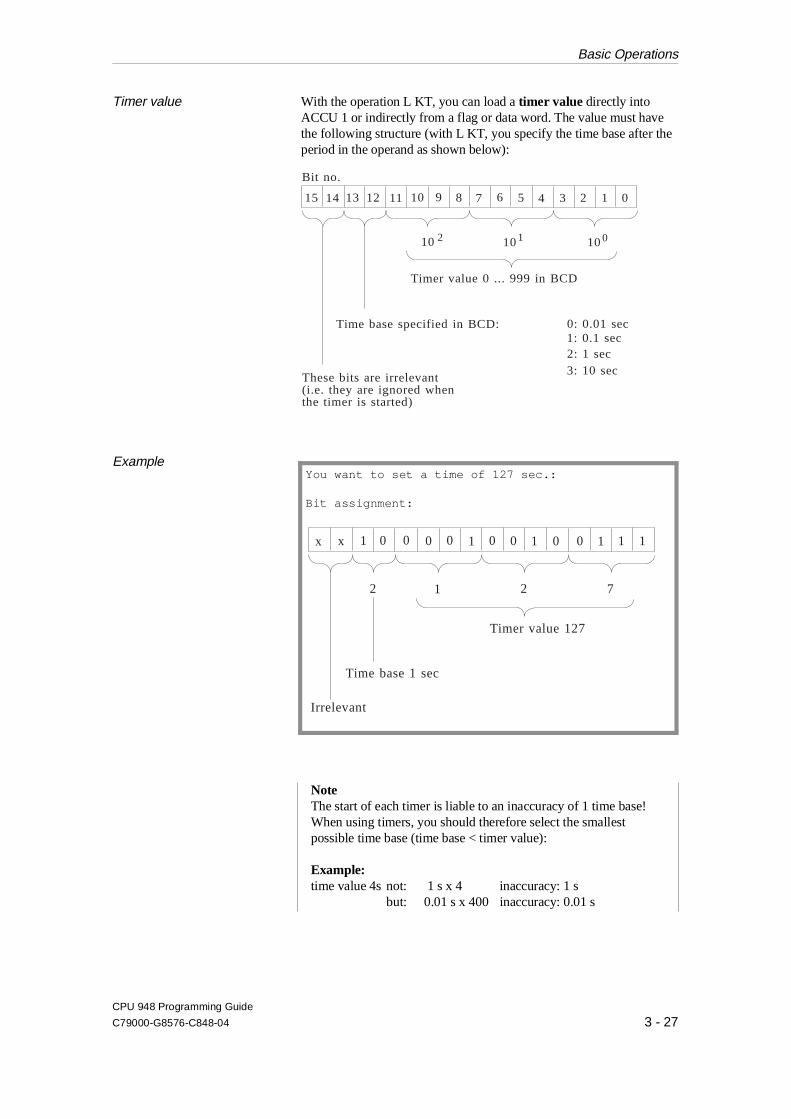
Timer value With the operation L KT, you can load a timer value directly intoACCU 1 or indirectly from a flag or data word. The value must havethe following structure (with L KT, you specify the time base after theperiod in the operand as shown below):
Example
NoteThe start of each timer is liable to an inaccuracy of 1 time base!When using timers, you should therefore select the smallestpossible time base (time base < timer value):
Example:time value 4s not: 1 s x 4 inaccuracy: 1 s
but: 0.01 s x 400 inaccuracy: 0.01 s
You want to set a time of 127 sec.:
Bit assignment:
Timer value 127
0 11 10 0 0 0 0 0 0x x 1 1 1
1 722
Irrelevant
Time base 1 sec
Bit no.
Timer value 0 ... 999 in BCD
012345678910111215 14 13
210 100101
These bits are irrelevant(i.e. they are ignored whenthe timer is started)
Time base specified in BCD: 0: 0.01 sec1: 0.1 sec2: 1 sec3: 10 sec
Basic Operations
CPU 948 Programming Guide
C79000-G8576-C848-04 3 - 27

Counter value With the operation L KC, you can load a counter value directly in ACCU 1 or indirectly from a flag or a data word. The value must have thefollowing structure:
Example
In the timer or counter itself, the value is in binary code. If you want toscan the timer or counter, you can load the actual timer or countervalue into ACCU 1 directly or in BCD code.
Counter value 127
0 11 10 0 0 0 0 0x x x x 1 1
1 72
Irrelevant
Bit no.
Counter value 0 ... 999specified in BCD
012345678910111215 14 13
10 2 100101
These bits are irrelevant,(i.e. they are ignored whenthe counter is set)
You want to specify a counter value of 127:
Bit assignment:
Basic Operations
CPU 948 Programming Guide
3 - 28 C79000-G8576-C848-04
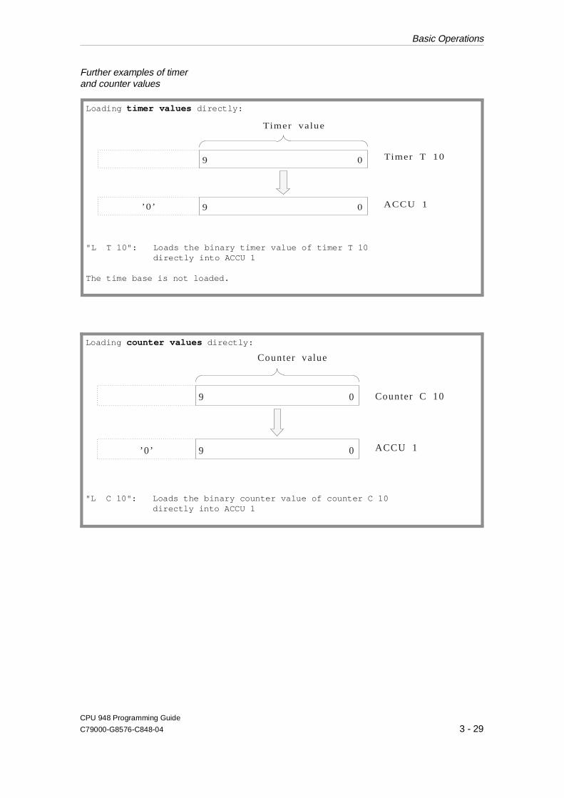
Further examples of timer and counter values
Loading timer values directly:
"L T 10": Loads the binary timer value of timer T 10directly into ACCU 1
The time base is not loaded.
Loading counter values directly:
"L C 10": Loads the binary counter value of counter C 10directly into ACCU 1
Counter value
Counter C 10
ACCU 19 0’0’
9 0
9 0
9 0
Timer value
Timer T 10
ACCU 1’0’
Basic Operations
CPU 948 Programming Guide
C79000-G8576-C848-04 3 - 29
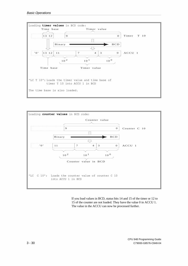
If you load values in BCD, status bits 14 and 15 of the timer or 12 to15 of the counter are not loaded. They have the value 0 in ACCU 1.The value in the ACCU can now be processed further.
Timer value
Timer T 10
ACCU 1
10 2 100101
9 01213
1213 0347811’0’
Time base Timer value
Time base
Binary BCD
Counter value
Counter C 10
ACCU 1
10 2 100101
Counter value in BCD
Binary BCD
9 0
0347811’0’
Loading timer values in BCD code:
"LC T 10": Loads the timer value and time base oftimer T 10 into ACCU 1 in BCD
The time base is also loaded.
Loading counter values in BCD code:
"LC C 10": Loads the counter value of counter C 10into ACCU 1 in BCD
Basic Operations
CPU 948 Programming Guide
3 - 30 C79000-G8576-C848-04

Arithmetic operations
Operation Operand Function
+ F- Fx F: F
+ G- Gx G: G
– Add two fixed point numbers (16 bits)Subtract one fixed point number from another (16 bits)Multiply two fixed point numbers (16 bits)Divide one fixed point number by another (16 bits):
quotient in ACCU-1-L, remainder in ACCU-1-H
Add two floating point numbers (32 bits)Subtract one floating point number from another (32 bits)Multiply two floating point numbers (32 bits)Divide one floating point number by another (32 bits)
Arithmetic operations logically combine the contents of ACCU 1 andACCU 2 (e.g. ACCU 2 - ACCU 1). The result is then contained inACCU 1. An arithmetic operation changes the arithmetic registers asfollows (in fixed point operations only the low word):
NoteWithin the supplementary operations, there are operations forsubtraction and addition of double word fixed point numbers.
Table 3-7 Arithmetic operations
ACCU 1 ACCU 2 ACCU 3 ACCU 4
before: <ACCU 1> <ACCU 2> <ACCU 3> <ACCU 4>
after: <result> <ACCU 3> <ACCU 4> <ACCU 4>
Basic Operations
CPU 948 Programming Guide
C79000-G8576-C848-04 3 - 31
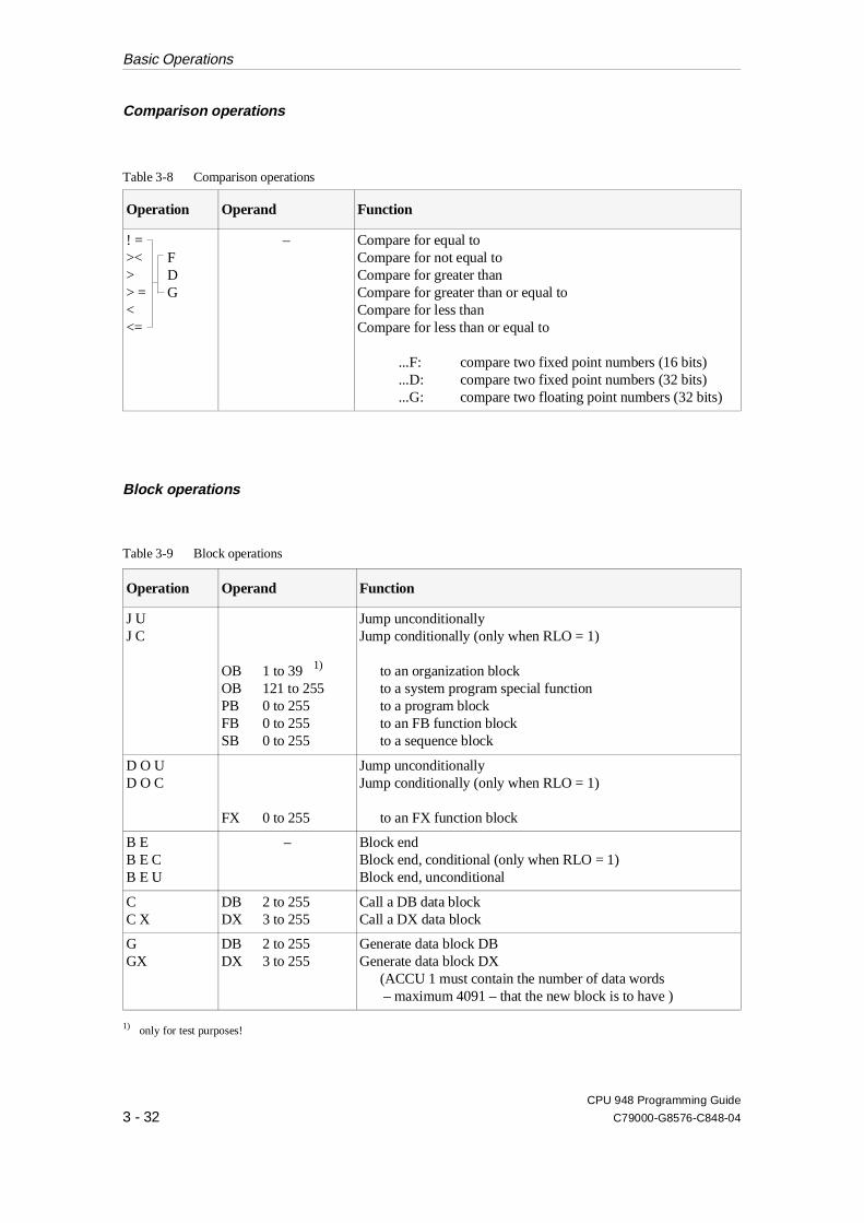
Comparison operations
Operation Operand Function
! =>< F> D> = G<<=
– Compare for equal toCompare for not equal toCompare for greater thanCompare for greater than or equal toCompare for less thanCompare for less than or equal to
...F: compare two fixed point numbers (16 bits)
...D: compare two fixed point numbers (32 bits)
...G: compare two floating point numbers (32 bits)
Block operations
Operation Operand Function
J UJ C
OB 1 to 39 1)
OB 121 to 255PB 0 to 255FB 0 to 255SB 0 to 255
Jump unconditionallyJump conditionally (only when RLO = 1)
to an organization blockto a system program special functionto a program blockto an FB function block to a sequence block
D O UD O C
FX 0 to 255
Jump unconditionallyJump conditionally (only when RLO = 1)
to an FX function block
B EB E CB E U
– Block endBlock end, conditional (only when RLO = 1)Block end, unconditional
CC X
DB 2 to 255DX 3 to 255
Call a DB data blockCall a DX data block
GGX
DB 2 to 255 DX 3 to 255
Generate data block DBGenerate data block DX
(ACCU 1 must contain the number of data words – maximum 4091 – that the new block is to have )
1) only for test purposes!
Table 3-8 Comparison operations
Table 3-9 Block operations
Basic Operations
CPU 948 Programming Guide
3 - 32 C79000-G8576-C848-04
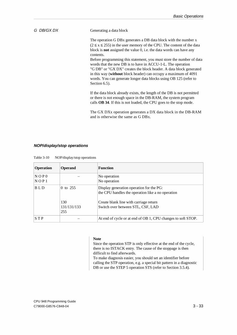
G DB/GX DX Generating a data block
The operation G DBx generates a DB data block with the number x(2 ≤ x ≤ 255) in the user memory of the CPU. The content of the datablock is not assigned the value 0, i.e. the data words can have anycontents.Before programming this statement, you must store the number of datawords that the new DB is to have in ACCU-1-L. The operation"G DB" or "GX DX" creates the block header. A data block generatedin this way (without block header) can occupy a maximum of 4091words. You can generate longer data blocks using OB 125 (refer toSection 6.5).
If the data block already exists, the length of the DB is not permittedor there is not enough space in the DB-RAM, the system programcalls OB 34. If this is not loaded, the CPU goes to the stop mode.
The GX DXx operation generates a DX data block in the DB-RAMand is otherwise the same as G DBx.
NOP/display/stop operations
Operation Operand Function
N O P 0N O P 1
– No operation No operation
B L D 0 to 255
130131/131/133255
Display generation operation for the PG: the CPU handles the operation like a no operation
Create blank line with carriage returnSwitch over between STL, CSF, LAD
S T P – At end of cycle or at end of OB 1, CPU changes to soft STOP.
NoteSince the operation STP is only effective at the end of the cycle,there is no ISTACK entry. The cause of the stoppage is thendifficult to find afterwards.To make diagnosis easier, you should set an identifier beforecalling the STP operation, e.g. a special bit pattern in a diagnosticDB or use the STEP 5 operation STS (refer to Section 3.5.4).
Table 3-10 NOP/display/stop operations
Basic Operations
CPU 948 Programming Guide
C79000-G8576-C848-04 3 - 33

3.5.2Programming Examples inthe STL, LAD and CSFMethods of Representation
Logic operations
I 1.7
I 1.3
I 1.1
Q 3.5
Logical/circuit diagramSTEP 5 representation
Ladder Control system
A I 1.1
A
A
I 1.3
I 1.7
= Q3.5
I 1.1 I 1.3 I 1.7 Q 3.5I 1.1 1.3 1.7
Q 3.5
&
Output Q 3.5 is "1" when all inputs are "1" simultaneously
I 1.1
I 1.3
I 1.7 Q 3.5
&
Statementlist
AND operation
diagram flowchart
Output Q 3.5 is "0" if any of the inputs has signal state "0"
The number of scans and the sequence of the logicstatements are optional
Programming Examples in the STL, LAD and CSF Methods of Representation
CPU 948 Programming Guide
3 - 34 C79000-G8576-C848-04
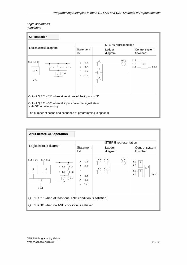
Logic operations (continued)
O I 1.2
O
O
I 1.7
I 1.5
= Q3.2
I 1.2
I 1.7
I 1.5
Q 3.2
state "0" simultaneously
Output Q 3.2 is "1" when at least one of the inputs is "1"
I 1.5I 1.7I 1.2
Q 3.2
I 1.2 1.7 1.5
Q 3.2
I 1.2
I 1.7
I 1.5 Q 3.2
1
1
Logical/circuit diagramSTEP 5 representation
Ladder Control systemStatementlist
OR operation
diagram flowchart
Output Q 3.2 is "0" when all inputs have the signal state
The number of scans and sequence of programming is optional
I 1.5 I 1.6
I 1.4
Q 3.1
Q 3.1 is "1" when at least one AND condition is satisfied
I 1.1
I 1.7
Q 3.1
&
I 1.6
I 1.5
Q 3.1
I 1.3
I 1.4
I 1.5 I 1.6
Q 3.1
&
I 1.4 I 1.3
&
A I 1.5
A
A
I 1.6
I 1.3
= Q3.1
O
A I 1.4
I 1.3I 1.1
I 1.7
&
1
1
Logical/circuit diagramSTEP 5 representation
Ladder Control systemStatementlist
AND-before-OR operation
diagram flowchart
Q 3.1 is "0" when no AND condition is satisfied
Programming Examples in the STL, LAD and CSF Methods of Representation
CPU 948 Programming Guide
C79000-G8576-C848-04 3 - 35

Logic operations (continued)
I 6.0
I 6.3
I 6.2
Q 2.1
Output Q 2.1 is "1" when input I 6.0 or input I 6.1 and oneof the inputs I 6.2 or I 6.3 has signal state "1"
Output Q 2.1 is "0" when input I 6.0 has signal state "0"and the AND condition is not satisfied
I 6.1
&
I 6.0 I 6.1 I 6.2 I 6.3
Q 2.1
I 6.0 I 6.2 I 6.3
I 6.1
Q 2.1
A I 6.0
O
O I 6.2
= Q2.1
A I 6.1
O I 6.3
)
I 6.0
I 6.1
I 6.2
I 6.3
Q 2.1
&1
1
1
1
A (
Logical/circuit diagramSTEP 5 representation
Ladder Control systemStatementlist
OR-before-AND operation /1st example
diagram flowchart
OR-before-AND operation
I 1.4 I 2..0
I 1.5
Q 3.0
Output Q 3.0 is "1" when both OR conditions are satisifed
I 1.4
I 1.5
Q 3.0
I 2.1I 2.0
I 2.1
I 1.4 I 1.5
Q 3.0
I 2.0 I 2.1
&
I 2..0
I 1.4
Q3.0
I 2.1
I 1.5
O I 1.4
O
O
I 1.5
I 2.1
= Q3.0
)
O I 2.0
)
&
1
1 1
A (
1
A (
Logical/circuit diagramSTEP 5 representation
Ladder diagram Control systemStatementlist
/2nd example
flowchart
Output Q 3.0 is "0" when at least one OR condition is not satisfied
Programming Examples in the STL, LAD and CSF Methods of Representation
CPU 948 Programming Guide
3 - 36 C79000-G8576-C848-04
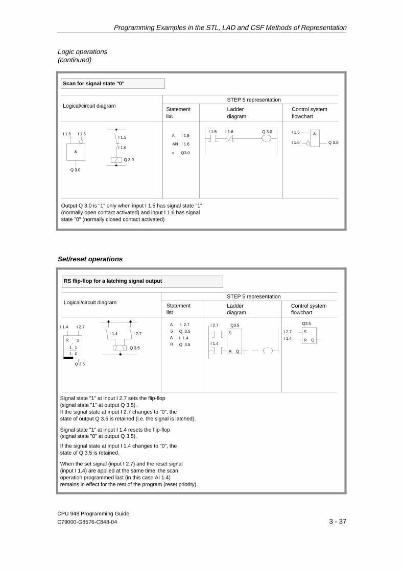
Logic operations (continued)
Set/reset operations
I 1.5 Q 3.0I 1.5 I 1.6
Q 3.0
&I 1.6
I 1.5
Q 3.0
A I 1.5
AN I 1.6
= Q3.0
I 1.6 I 1.5
I 1.6 Q 3.0
&
Output Q 3.0 is "1" only when input I 1.5 has signal state "1"
state "0" (normally closed contact activated)(normally open contact activated) and input I 1.6 has signal
Logical/circuit diagramSTEP 5 representation
Ladder Control systemStatementlist
Scan for signal state "0"
diagram flowchart
I 1.4 I 2.7
I 2.7
Q 3.5
I 1.4
Q 3.5
I 2.7 Q3.5
I 1.4
S
R Q
A I 2.7
I 1.4
Q 3.5
S
R
Q 3.5
AI 2.7
I 1.4
Q3.5
R
S
Q R S
1 1
1 0
Signal state "1" at input I 2.7 sets the flip-flop(signal state "1" at output Q 3.5).If the signal state at input I 2.7 changes to "0", the state of output Q 3.5 is retained (i.e. the signal is latched).
If the signal state at input I 1.4 changes to "0", thestate of Q 3.5 is retained.
Signal state "1" at input I 1.4 resets the flip-flop(signal state "0" at output Q 3.5).
When the set signal (input I 2.7) and the reset signal(input I 1.4) are applied at the same time, the scan operation programmed last (in this case AI 1.4)remains in effect for the rest of the program (reset priority).
Logical/circuit diagramSTEP 5 representation
Ladder Control systemStatementlist
RS flip-flop for a latching signal output
diagram flowchart
Programming Examples in the STL, LAD and CSF Methods of Representation
CPU 948 Programming Guide
C79000-G8576-C848-04 3 - 37
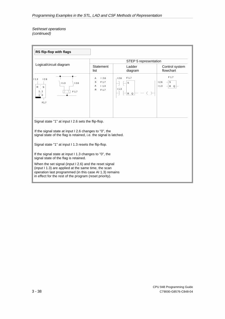
Set/reset operations(continued)
I 1.3 I 2.6
I 2.6
F1.7
I 1.3
F 1.7
I 2.6 F 1.7
I 1.3
S
R Q
A I 2.6
I 1.3
F 1.7
S
R
F 1.7
A
I 2.6
I 1.3
F 1.7
S
R S
1 1
1 0
Signal state "1" at input I 2.6 sets the flip-flop.
If the signal state at input I 1.3 changes to "0", thesignal state of the flag is retained.
When the set signal (input I 2.6) and the reset signal(input I 1.3) are applied at the same time, the scanoperation last programmed (in this case AI 1.3) remainsin effect for the rest of the program (reset priority).
Signal state "1" at input I 1.3 resets the flip-flop.
If the signal state at input I 2.6 changes to "0", thesignal state of the flag is retained, i.e. the signal is latched.
R Q
Logical/circuit diagramSTEP 5 representation
Ladder Control systemStatementlist
RS flip-flop with flags
flowchartdiagram
Programming Examples in the STL, LAD and CSF Methods of Representation
CPU 948 Programming Guide
3 - 38 C79000-G8576-C848-04
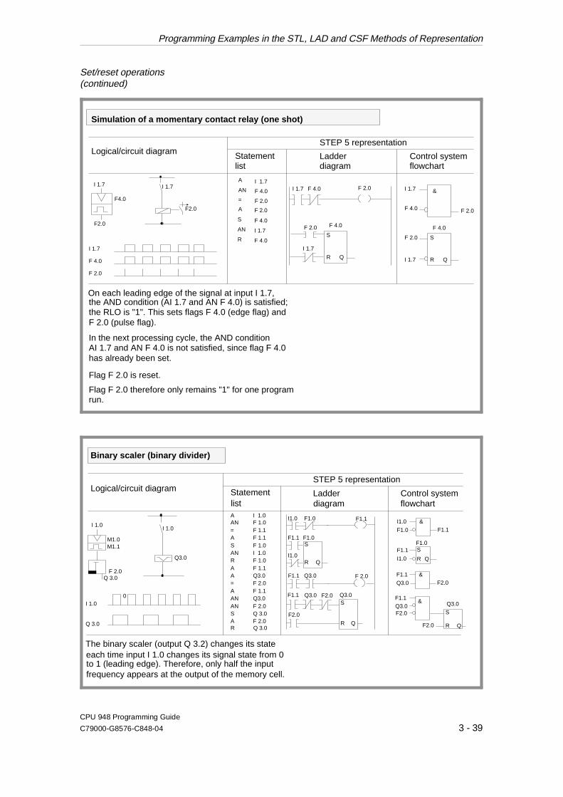
Set/reset operations(continued)
On each leading edge of the signal at input I 1.7,the AND condition (AI 1.7 and AN F 4.0) is satisfied;the RLO is "1". This sets flags F 4.0 (edge flag) andF 2.0 (pulse flag).
Flag F 2.0 is reset.
In the next processing cycle, the AND conditionAI 1.7 and AN F 4.0 is not satisfied, since flag F 4.0has already been set.
Flag F 2.0 therefore only remains "1" for one programrun.
I 1.7
F 4.0
F 2.0
I 1.7
F2.0
F4.0
I 1.7
F2.0
A
AN
=
A
S
AN
R
I 1.7
F 4.0
F 2.0
F 2.0
F 4.0
I 1.7
F 4.0
Logical/circuit diagramSTEP 5 representation
Ladder Control systemStatementlist
Simulation of a momentary contact relay (one shot)
diagram flowchart
I 1.7
F 2.0
I 1.7
F 4.0
F 2.0
F 4.0
S
R Q
&F 2.0I 1.7 F 4.0
S
R Q
F 4.0F 2.0
I 1.7
I 1.0
I 1.0
A I 1.0
Q3.0
I 1.0
M1.0M1.1
F 2.0Q 3.0
AN F 1.0= F 1.1
F 1.1AF 1.0SI 1.0ANF 1.0R
A F 1.1A Q3.0= F 2.0A F 1.1AN Q3.0
Q 3.0SAN F 2.0
A F 2.0R Q 3.0
The binary scaler (output Q 3.2) changes its state
to 1 (leading edge). Therefore, only half the inputfrequency appears at the output of the memory cell.
each time input I 1.0 changes its signal state from 0
F1.1 Q3.0 F 2.0
S
R Q
F1.1
I1.0
F1.0
I1.0 F1.0 F1.1
S
R Q
F1.1 Q3.0 F2.0 Q3.0
F2.0
0
&
I1.0
F1.0
&F1.1
F1.1
I1.0
SF1.0
R Q
F1.1Q3.0F2.0
F2.0
Q3.0
S
R Q
F1.1
Q3.0
&F2.0
Q 3.0
Logical/circuit diagramSTEP 5 representation
Ladder Control systemStatementlist
Binary scaler (binary divider)
diagram flowchart
Programming Examples in the STL, LAD and CSF Methods of Representation
CPU 948 Programming Guide
C79000-G8576-C848-04 3 - 39

Timer operations
Subsequent scans with an RLO of "1" do not affect the
If the RLO is "0", the timer is reset (cleared).
timer.
KT 10.2:
the time base:0 = 0.1sec 2 = 1sec
The timer is loaded with the specified value (10).The number to the right of the decimal point indicates
BI and DE are digital outputs of the timer. The time atoutput BI is in binary code. The time at DE is in BCD codewith time base.
I 3.0
Q4.0
T
as the timer is running.
Q4.0
The timer is started during the first scan if the RLO is "1".
I 3.0
T 1
R S10s
1
I 3.0
T 1
Q4.0
I 3.0
Q
10.2
T1
BI
Q4.0
QW0
DE QW2
I 3.0
Q
10.2
T1
1
TV BI
Q4.0
QW0
DE QW2
R
Logical/circuit diagramSTEP 5 representation
Ladder Control systemStatementlist
Pulse timer
=
SP T 1L KT 10.2A I 3.0
AN I 3.0R T 1L T 1T QW 0LC T 1T QW 2A T 1= Q 4.0
1
TV
R
diagram flowchart
The scan AT or OT produces the signal "1" as long
3 = 10 sec1 = 0.1 sec
KT KT
I 3.0
Programming Examples in the STL, LAD and CSF Methods of Representation
CPU 948 Programming Guide
3 - 40 C79000-G8576-C848-04

Timer operations (continued)
The timer is started during the first scan if the RLO is"1".
A I 3.1L IW 15SE T 2
T 2AQ 4.1=
I 3.1
Q
IW15
T2
1
TW BI
Q4.1
DE
I 3.1
Q
IW15
T2
1
TW BI
Q4.1
DE
R
Q4.1
V
R
V
Q4.1
I 3.1
T 2
R S
1
T2
I 3.1
T 2
(IB 15) (IB 16)An RLO of "0" does not affect the timer.
The scan AT or OT produces a signal "1" as long as the timer is running.
IW 15:Set the timer with the value of the operand I, Q, F orD in BCD code (in this example, input word 15).
I 3.1
Q4.1T T
Timer valueTimebase
5 43 0 7 4 3 0
01010 110 2
Logical/circuit diagramSTEP 5 representation
Ladder Control systemStatementlist
Extended pulse timer
=
diagram flowchart
Programming Examples in the STL, LAD and CSF Methods of Representation
CPU 948 Programming Guide
C79000-G8576-C848-04 3 - 41
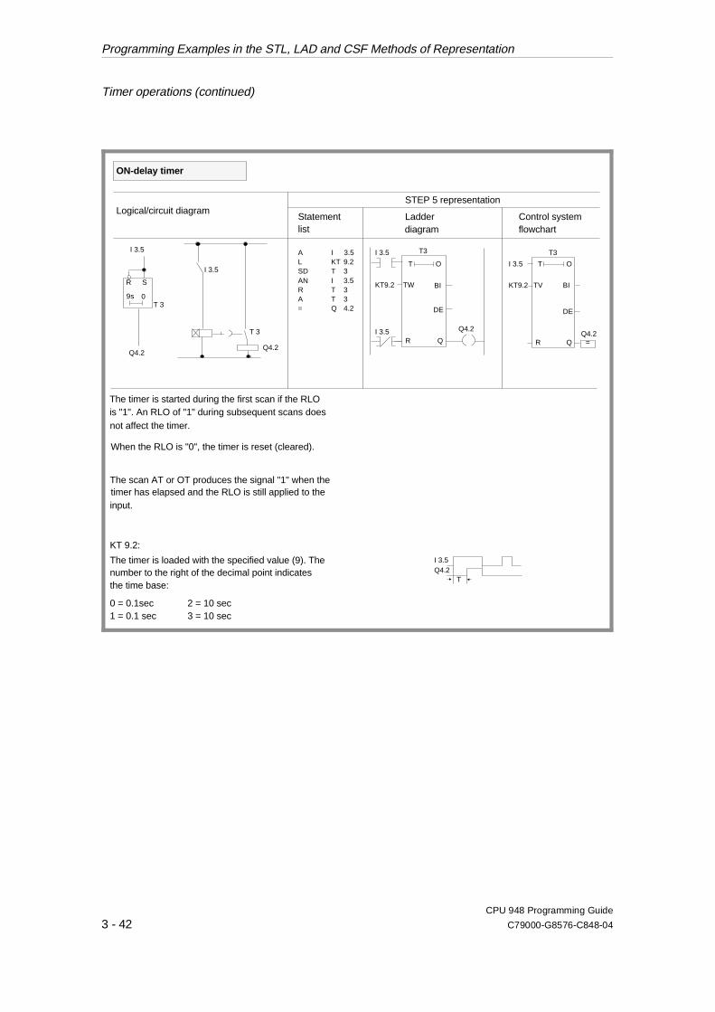
Timer operations (continued)
The timer is started during the first scan if the RLOis "1". An RLO of "1" during subsequent scans does
Q
KT9.2
T3
TW BI
Q4.2
DE
I 3.5
Q
KT9.2
T3
TV
Q4.2
DE
RQ4.2
R
I 3.5
T 3
R S
I 3.5
T 3
9s 0
Q4.2
BI
T O T O
When the RLO is "0", the timer is reset (cleared).
not affect the timer.
KT 9.2:
The timer is loaded with the specified value (9). Thenumber to the right of the decimal point indicates
0 = 0.1sec 2 = 10 sec
I 3.5Q4.2
T
The scan AT or OT produces the signal "1" when thetimer has elapsed and the RLO is still applied to theinput.
Logical/circuit diagramSTEP 5 representation
Ladder Control systemStatementlist
ON-delay timer
IKTTITTQ
3.59.233.5334.2
ALSDANRA=
I 3.5
I 3.5
=
diagram flowchart
the time base:
3 = 10 sec1 = 0.1 sec
Programming Examples in the STL, LAD and CSF Methods of Representation
CPU 948 Programming Guide
3 - 42 C79000-G8576-C848-04
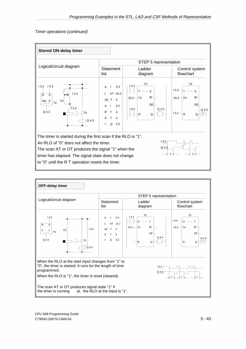
Timer operations (continued)
T S
TV BI
DE
R Q
I 3.3
Q 4.3
I 3.2 I 3.3
Q 4.3 T4
Q 4.3
R S
20s 0
I 3.3
T4
I 3.2 I 3.2
T S
BI
DE
R Q
I 3.3
I 3.2
T4 T4
I 3.3
Q 4.3
T Ttimer has elapsed. The signal state does not change
to "0" until the R T operation resets the timer.
The timer is started during the first scan if the RLO is "1".
An RLO of "0" does not affect the timer.
T4
= Q 4.3
A I 3.3
L KT 20.2
SS T 4
A I 3.2
R T 4
A T 4
E
The scan AT or OT produces the signal "1" when the
Logical/circuit diagramSTEP 5 representation
Ladder Control systemStatementlist
Stored ON-delay timer
20.2 TV
Q 4.3=
20.2
diagram flowchart
I 3.4
Q 4.4
I 3.4
Q 4.4 T5
Q 4.4
R S
0 1 I 3.4T5
O T
TVBI
DE
R Q
O T
BI
DE
R Q
I 3.4
T5 T5
T5
A I
= Q
3.4
L KT 10.1
SF T 5
A T 5
4.3
I 3.4
Q 4.4
T TT
The scan AT or OT produces signal state "1" ifthe timer is running
When the RLO is "1", the timer is reset (cleared).
When the RLO at the start input changes from "1" to"0", the timer is started. It runs for the length of time programmed.
Logical/circuit diagramSTEP 5 representation
Ladder Control systemStatementlist
OFF-delay timer
10.1 TV 10.1
Q 4.4=
diagram flowchart
or the RLO at the input is "1".
Programming Examples in the STL, LAD and CSF Methods of Representation
CPU 948 Programming Guide
C79000-G8576-C848-04 3 - 43
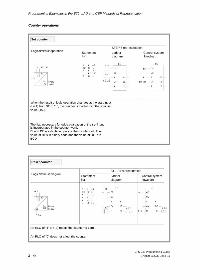
Counter operations
When the result of logic operation changes at the start input(I 4.1) from "0" to "1", the counter is loaded with the specified
is incorporated in the counter word.BI and DE are digital outputs of the counter cell. The value at BI is in binary code and the value at DE is inBCD.
I 4.1
R S
CQ
CI
+
binary16 bits
KC 150
KC 150
CD
BI
DE
R Q
C1
CU
S
CV
I 4.1
CD
BI
DE
R Q
C1
CU
S
CV
value (150).
Logical/circuit operationSTEP 5 representation
Ladder Control systemStatement list
Set counter
I 4.1
I 4.0
I 4.0
ACUALS
I CIKCC
4.014.11501
diagram flowchart
The flag necessary for edge evaluation of the set input
KC 150
I 4.2
R S CI
binary16 bits
CU
BI
DE
R Q
C2
CD
S
CV
An RLO of "1" (I 4.2) resets the counter to zero.
Q 2.4
Q 2.4CQI 4.2
CU
BI
DE
R Q
C2
CD
S
CVQ 2.4=0 /
An RLO of "0" does not affect the counter.
Logical/circuit diagramSTEP 5 representation
Ladder Control systemStatementlist
Reset counter
ACDARA=
I
CICCQ
4.024.2222.4
I 4.2
I 4.0
I 4.0
=
diagram flowchart
Programming Examples in the STL, LAD and CSF Methods of Representation
CPU 948 Programming Guide
3 - 44 C79000-G8576-C848-04
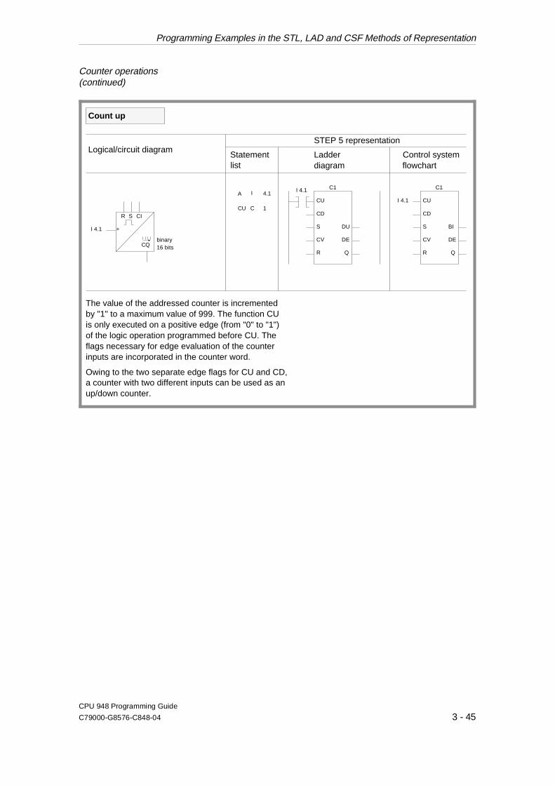
Counter operations(continued)
I 4.1
R S
CQ
CI
+
binary16 bits
CD
BI
DE
R Q
C1
CU
S
CV
Owing to the two separate edge flags for CU and CD,a counter with two different inputs can be used as anup/down counter.
The value of the addressed counter is incremented by "1" to a maximum value of 999. The function CUis only executed on a positive edge (from "0" to "1")of the logic operation programmed before CU. Theflags necessary for edge evaluation of the counterinputs are incorporated in the counter word.
I 4.1
A I 4.1
CU C 1CD
DU
DE
R Q
C1
CU
S
CV
I 4.1
Logical/circuit diagramSTEP 5 representation
Ladder Control systemStatementlist
Count up
diagram flowchart
Programming Examples in the STL, LAD and CSF Methods of Representation
CPU 948 Programming Guide
C79000-G8576-C848-04 3 - 45
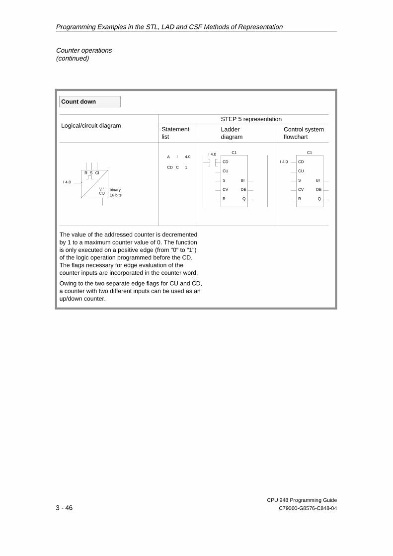
Counter operations(continued)
I 4.0
R S CI
-
binary16 bits
CU
BI
DE
R Q
C1
CD
S
CV
Owing to the two separate edge flags for CU and CD,a counter with two different inputs can be used as anup/down counter.
The value of the addressed counter is decrementedby 1 to a maximum counter value of 0. The functionis only executed on a positive edge (from "0" to "1")of the logic operation programmed before the CD.The flags necessary for edge evaluation of the counter inputs are incorporated in the counter word.
I 4.0
A I 4.0
CD C 1CU
BI
DE
R Q
C1
CD
S
CV
I 4.0
CQ
Logical/circuit diagramSTEP 5 representation
Ladder Control systemStatementlist
Count down
diagram flowchart
Programming Examples in the STL, LAD and CSF Methods of Representation
CPU 948 Programming Guide
3 - 46 C79000-G8576-C848-04
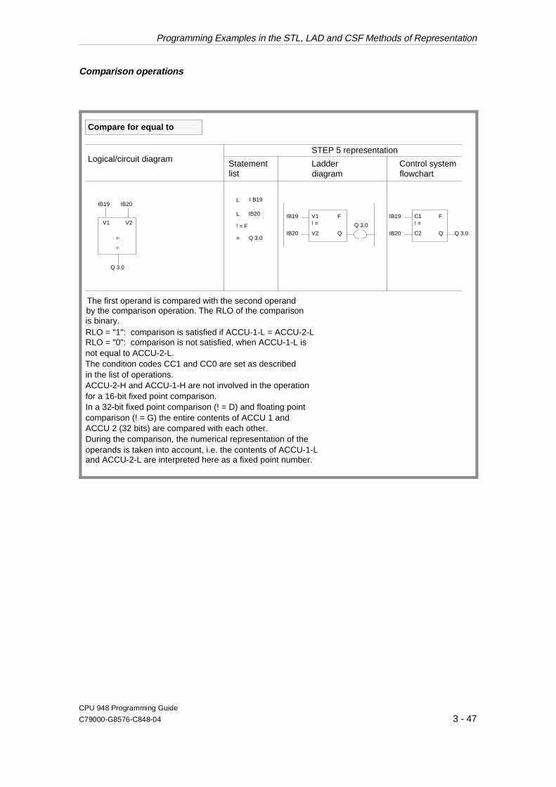
Comparison operations
V1
V2
! =F
QQ 3.0
L I B19
L IB20
! = F
= Q 3.0
IB19
IB20 Q 3.0
IB19
IB20
C1
C2
! =F
Q
not equal to ACCU-2-L.
in the list of operations.ACCU-2-H and ACCU-1-H are not involved in the operationfor a 16-bit fixed point comparison.In a 32-bit fixed point comparison (! = D) and floating pointcomparison (! = G) the entire contents of ACCU 1 and ACCU 2 (32 bits) are compared with each other.During the comparison, the numerical representation of theoperands is taken into account, i.e. the contents of ACCU-1-L
The first operand is compared with the second operandby the comparison operation. The RLO of the comparisonis binary.
Q 3.0
=
V1 V2
=
IB19 IB20
The condition codes CC1 and CC0 are set as described
RLO = "0": comparison is not satisfied, when ACCU-1-L is
Logical/circuit diagramSTEP 5 representation
Ladder Control systemStatementlist
Compare for equal to
RLO = "1": comparison is satisfied if ACCU-1-L = ACCU-2-L
diagram flowchart
and ACCU-2-L are interpreted here as a fixed point number.
Programming Examples in the STL, LAD and CSF Methods of Representation
CPU 948 Programming Guide
C79000-G8576-C848-04 3 - 47
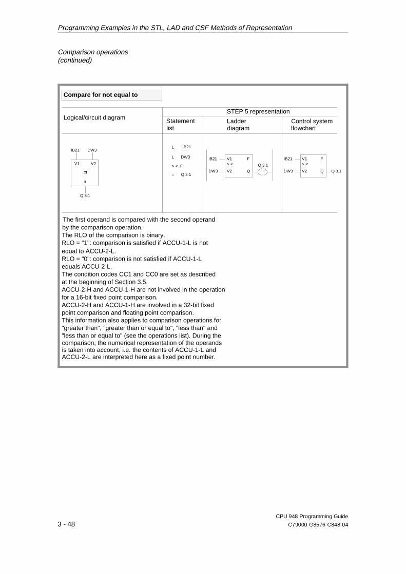
Comparison operations(continued)
Q 3.1
L I B21
L DW3
> < F
= Q 3.1
IB21
DW3
V1
V2
> <F
Q Q 3.1
IB21
DW3
V1
V2
> <F
Q
RLO = "0": comparison is not satisfied if ACCU-1-L equals ACCU-2-L.The condition codes CC1 and CC0 are set as describedat the beginning of Section 3.5.ACCU-2-H and ACCU-1-H are not involved in the operationfor a 16-bit fixed point comparison.
This information also applies to comparison operations for"greater than", "greater than or equal to", "less than" and"less than or equal to" (see the operations list). During the
The first operand is compared with the second operandby the comparison operation.The RLO of the comparison is binary.
Q 3.1
V1 V2
IB21 DW3
=/=/
ACCU-2-H and ACCU-1-H are involved in a 32-bit fixedpoint comparison and floating point comparison.
RLO = "1": comparison is satisfied if ACCU-1-L is notequal to ACCU-2-L.
Logical/circuit diagramSTEP 5 representation
Ladder Control systemStatement list
Compare for not equal to
diagram flowchart
comparison, the numerical representation of the operandsis taken into account, i.e. the contents of ACCU-1-L andACCU-2-L are interpreted here as a fixed point number.
Programming Examples in the STL, LAD and CSF Methods of Representation
CPU 948 Programming Guide
3 - 48 C79000-G8576-C848-04
3.5.3Supplementary Operations You can use the supplementary operations set on the programmer only
in function blocks (FB and FX). This means that the total operationsset for function blocks consists of the basic operations and thesupplementary operations.
The system operations also belong to the supplementary functions.You can use the system operations, for example to overwrite thememory at optional locations or to change the contents of the workingregisters of the CPU. System operations can only be programmed ifthey have been enabled in the presets menu of the programmer (nolonger necessary from S5-DOS Version 2.0 upwards).
If you intend to use system operations, you should be familiar withChapter 9 "Memory access".
CautionOnly experienced system programmers should use the systemoperations and then only with extreme caution.
You can only write operations in function blocks in STL. You cannotprogram function blocks in graphic form (LAD and CSF methods ofrepresentation).This section describes the supplementary operations and covers possiblecombinations of substitution operations with actual operands.
System operations System operations are marked in the first column of the tables with S
Supplementary Operations
CPU 948 Programming Guide
C79000-G8576-C848-04 3 - 49

Binary logic operations
Operation Operand Function
A =
AN =
O =
ON =
AND operation, scan a formal operand for signal state ’1’
AND operation, scan a formal operand for signal state ’0’
OR operation, scan a formal operand for signal state ’1’
OR operation, scan a formal operand for signal state ’0’
Insert formal operand
Inputs, outputs, data and flags addressed in binary (parametertypes: I, Q; data type BI) and timers and counters (parametertype: T, C) are permitted as actual operands.
Digital logic operations
Operation Operand Function
AW
OW
XOW
AND operation on the contents of ACCU-1-L and ACCU-2-L
OR operation on the contents of ACCU-1-L and ACCU-2-L
Exklusive OR operation on the contents of ACCU-1-L andACCU-2-L
ACCUs 2, 3 and 4 are not affected, however, the condition codes CC 1 and CC 0 are affected (see word condition codes).
Table 3-11 Binary logic operations with formal operands
Table 3-12 Digital logic operations
Supplementary Operations
CPU 948 Programming Guide
3 - 50 C79000-G8576-C848-04
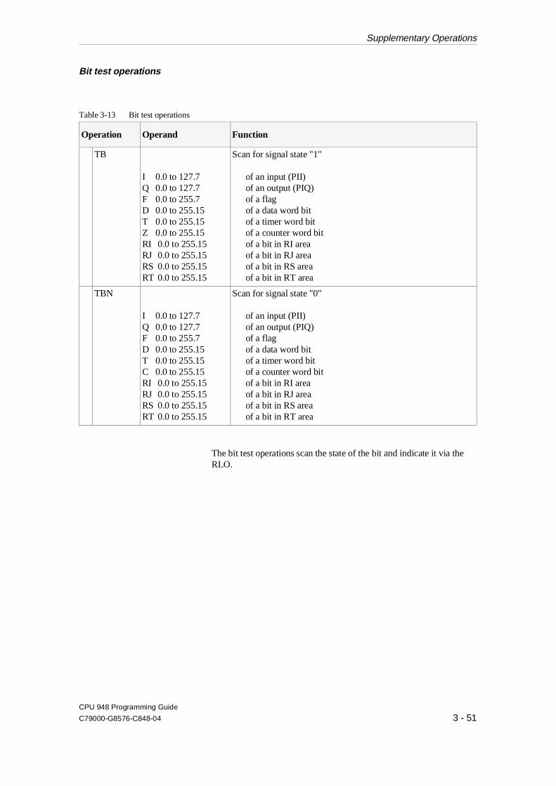
Bit test operations
Operation Operand Function
TB
I 0.0 to 127.7Q 0.0 to 127.7F 0.0 to 255.7D 0.0 to 255.15T 0.0 to 255.15Z 0.0 to 255.15RI 0.0 to 255.15RJ 0.0 to 255.15RS 0.0 to 255.15RT 0.0 to 255.15
Scan for signal state "1"
of an input (PII)of an output (PIQ)of a flagof a data word bitof a timer word bitof a counter word bitof a bit in RI areaof a bit in RJ areaof a bit in RS areaof a bit in RT area
TBN
I 0.0 to 127.7Q 0.0 to 127.7F 0.0 to 255.7D 0.0 to 255.15T 0.0 to 255.15C 0.0 to 255.15RI 0.0 to 255.15RJ 0.0 to 255.15RS 0.0 to 255.15RT 0.0 to 255.15
Scan for signal state "0"
of an input (PII)of an output (PIQ)of a flagof a data word bitof a timer word bitof a counter word bitof a bit in RI areaof a bit in RJ areaof a bit in RS areaof a bit in RT area
The bit test operations scan the state of the bit and indicate it via theRLO.
Table 3-13 Bit test operations
Supplementary Operations
CPU 948 Programming Guide
C79000-G8576-C848-04 3 - 51

Set/reset operations
Operation Operand Function
S =
RB =
RD=
= =
Set a formal operand (binary)
Reset a formal operand (binary)
Reset a formal operand (digital)for timers and counters
Assign the value of the RLO to aformal operand
Insert formal operand
Inputs, outputs and F flags addressed in binary (parameter type: I, Q; data type BI) are permitted as actual operands.
Operation Operand Function
SUI 0.0 to 127.7Q 0.0 to 127.7F 0.0 to 255.7D 0.0 to 255.15T 0.0 to 255.15C 0.0 to 255.15RI 0.0 to 255.15RJ 0.0 to 255.15RS 60.0 to 63.15RT 0.0 to 255.15
Unconditional settingof an input (PII)of an output (PIQ)of a flagof a data word bitof a timer word bitof a counter word bitof a bit in RI areaof a bit in RJ areaof a bit in RS areaof a bit in RT area
RUI 0.0 to 127.7Q 0.0 to 127.7F 0.0 to 255.7D 0.0 to 255.15T 0.0 to 255.15C 0.0 to 255.15RI 0.0 to 255.15RJ 0.0 to 255.15RS 60.0 to 63.15RT 0.0 to 255.15
Unconditional resettingof an input (PII)of an output (PIQ)of a flagof a data word bitof a timer word bitof a counter word bitof a bit in RI areaof a bit in RJ areaof a bit in RS areaof a bit in RT area
Table 3-14 Set/reset operations with formal operands
Table 3-15 Set and reset operations
Supplementary Operations
CPU 948 Programming Guide
3 - 52 C79000-G8576-C848-04
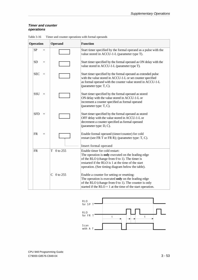
Timer and counteroperations
Operation Operand Function
SP =
SD =
SEC =
SSU =
SFD =
FR =
Start timer specified by the formal operand as a pulse with thevalue stored in ACCU-1-L (parameter type T).
Start timer specified by the formal operand as ON delay with thevalue stored in ACCU-1-L (parameter type T).
Start timer specified by the formal operand as extended pulse with the value stored in ACCU-1-L or set counter specified as formal operand with the counter value stored in ACCU-1-L(parameter type: T, C).
Start timer specified by the formal operand as stored ON delay with the value stored in ACCU-1-L or increment a counter specified as formal operand (parameter type: T, C). Start timer specified by the formal operand as stored OFF delay with the value stored in ACCU-1-L or decrement a counter specified as formal operand (parameter type: D, C).
Enable formal operand (timer/counter) for cold restart (see FR T or FR R); (parameter type: T, C).
Insert formal operand
FR T 0 to 255
C 0 to 255
Enable timer for cold restart:The operation is only executed on the leading edge of the RLO (change from 0 to 1). The timer is restarted if the RLO is 1 at the time of the start operation. (See timing diagram below the table).
Enable a counter for setting or resetting:The operation is executed only on the leading edge of the RLO (change from 0 to 1). The counter is only started if the RLO = 1 at the time of the start operation.
tt
RLOfor SP T
RLOfor FR T
Scanwith A T
Table 3-16 Timer and counter operations with formal operands
Supplementary Operations
CPU 948 Programming Guide
C79000-G8576-C848-04 3 - 53
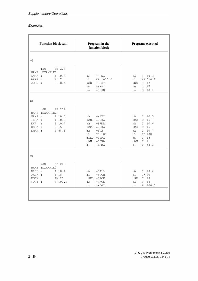
Examples
Function block call Program in the function block
Program executed
a)
:JU FB 203NAME :EXAMPLE1ANNA : I 10.3BERT : T 17JOHN : Q 18.4
:A =ANNA:L KT 010.2:SSU =BERT:U =BERT:= =JOHN
:A I 10.3:L KT 010.2:SS T 17:U T 17:= Q 18.4
b)
:JU FB 204NAME :EXAMPLE2MAXI : I 10.5IRMA : I 10.6EVA : I 10.7DORA : C 15EMMA : F 58.3
:A =MAXI:SSU =DORA:A =IRMA:SFD =DORA:A =EVA:L KC 100:SEC =DORA:AN =DORA:= =EMMA
:A I 10.5:CU C 15:A I 10.6:CD C 15:A I 10.7:L KC 100:S C 15:AN C 15:= F 58.3
c)
:JU FB 205NAME :EXAMPLE3BILL : I 10.4JACK : T 18EGON : IW 20YOGI : F 100.7
:A =BILL:L =EGON:SEC =JACK:A =JACK:= =YOGI
:A I 10.4:L IW 20:SE T 18:A T 18:= F 100.7
Supplementary Operations
CPU 948 Programming Guide
3 - 54 C79000-G8576-C848-04
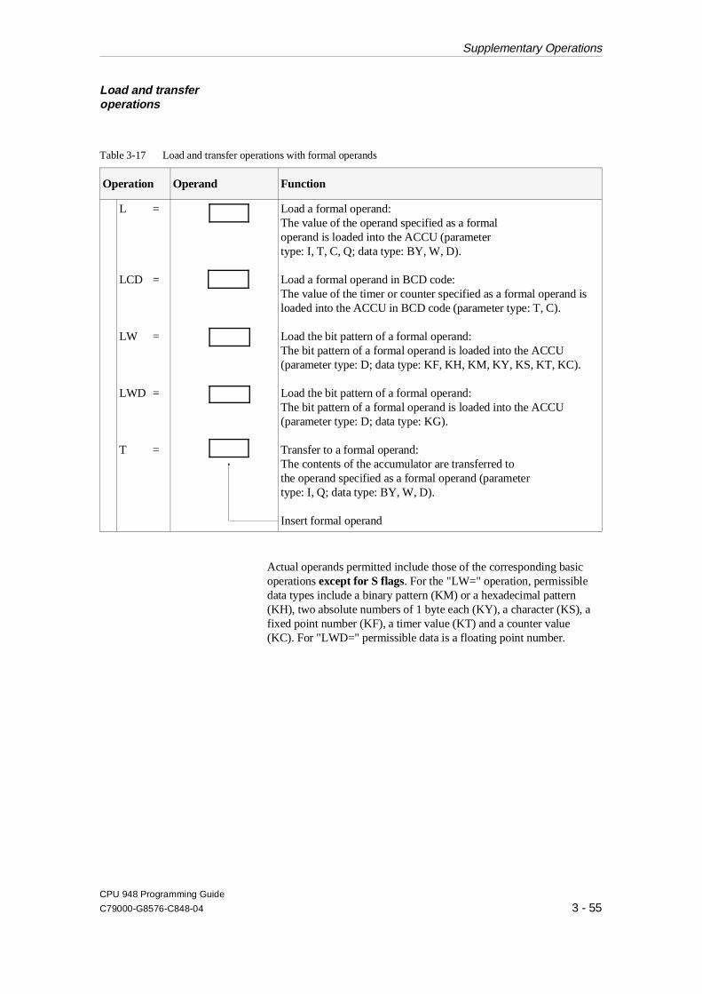
Load and transferoperations
Operation Operand Function
L =
LCD =
LW =
LWD =
T =
Load a formal operand:The value of the operand specified as a formal operand is loaded into the ACCU (parameter type: I, T, C, Q; data type: BY, W, D).
Load a formal operand in BCD code:The value of the timer or counter specified as a formal operand isloaded into the ACCU in BCD code (parameter type: T, C).
Load the bit pattern of a formal operand:The bit pattern of a formal operand is loaded into the ACCU(parameter type: D; data type: KF, KH, KM, KY, KS, KT, KC).
Load the bit pattern of a formal operand:The bit pattern of a formal operand is loaded into the ACCU(parameter type: D; data type: KG).
Transfer to a formal operand:The contents of the accumulator are transferred to the operand specified as a formal operand (parameter type: I, Q; data type: BY, W, D).
Insert formal operand
Actual operands permitted include those of the corresponding basicoperations except for S flags. For the "LW=" operation, permissibledata types include a binary pattern (KM) or a hexadecimal pattern(KH), two absolute numbers of 1 byte each (KY), a character (KS), afixed point number (KF), a timer value (KT) and a counter value(KC). For "LWD=" permissible data is a floating point number.
Table 3-17 Load and transfer operations with formal operands
Supplementary Operations
CPU 948 Programming Guide
C79000-G8576-C848-04 3 - 55
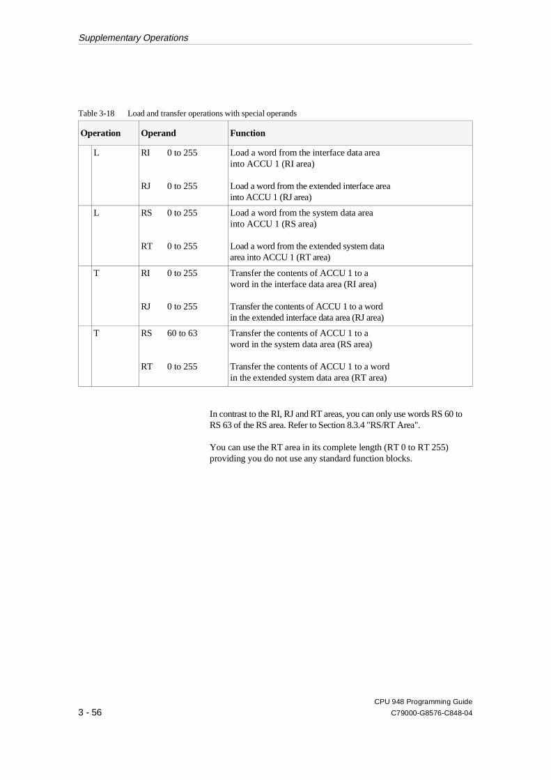
Operation Operand Function
L RI 0 to 255
RJ 0 to 255
Load a word from the interface data area into ACCU 1 (RI area)
Load a word from the extended interface area into ACCU 1 (RJ area)
L RS 0 to 255
RT 0 to 255
Load a word from the system data area into ACCU 1 (RS area)
Load a word from the extended system data area into ACCU 1 (RT area)
T RI 0 to 255
RJ 0 to 255
Transfer the contents of ACCU 1 to a word in the interface data area (RI area)
Transfer the contents of ACCU 1 to a word in the extended interface data area (RJ area)
T RS 60 to 63
RT 0 to 255
Transfer the contents of ACCU 1 to a word in the system data area (RS area)
Transfer the contents of ACCU 1 to a word in the extended system data area (RT area)
In contrast to the RI, RJ and RT areas, you can only use words RS 60 toRS 63 of the RS area. Refer to Section 8.3.4 "RS/RT Area".
You can use the RT area in its complete length (RT 0 to RT 255)providing you do not use any standard function blocks.
Table 3-18 Load and transfer operations with special operands
Supplementary Operations
CPU 948 Programming Guide
3 - 56 C79000-G8576-C848-04
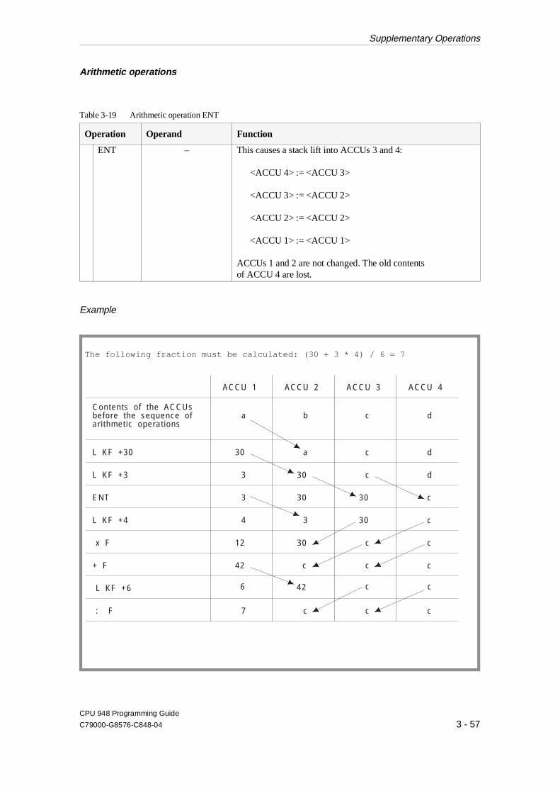
Arithmetic operations
Operation Operand Function
ENT – This causes a stack lift into ACCUs 3 and 4:
<ACCU 4> := <ACCU 3>
<ACCU 3> := <ACCU 2>
<ACCU 2> := <ACCU 2>
<ACCU 1> := <ACCU 1>
ACCUs 1 and 2 are not changed. The old contentsof ACCU 4 are lost.
Example
ACCU 1 ACCU 2 ACCU 3 ACCU 4
L KF +30 d30 ca
L KF +3 d3 c30
aContents of the ACCUsbefore the sequence ofar i thmetic operat ions
b c d
x F c12 c30
+ F c42 cc
L KF +4 c4 303
ENT 3 30 30 c
c7 cc
L KF +6 c6 c42
: F
Table 3-19 Arithmetic operation ENT
The following fraction must be calculated: (30 + 3 * 4) / 6 = 7
Supplementary Operations
CPU 948 Programming Guide
C79000-G8576-C848-04 3 - 57

Operation Operand Function
S ADD BN -128 to+127
Add a byte constant (fixed point) to ACCU-1-L (includessign change)/the condition code in CC 0, CC 1, OV and OS are not affected! – ACCU-1-H and ACCUs 2 to 4 remain unchanged.
S ADD KF -32 768 to+32 767
Add a fixed point constant (word) to ACCU-1-L/ the condition codes in CC 0, CC 1, OV and OS are notaffected! – ACCU-1-H and ACCUs 2 to 4 remain unchanged.
S ADD 1) DH 0000 0000toFFFF FFFF
Add a double word fixed point constant to ACCU 1/thecondition codes in CC 0, CC 1, OV and OS are not affected! –ACCUs 2 to 4 remain unchanged.
S +D 1) Add two double word fixed point constants (ACCU 2 + ACCU 1)/the result can be evaluated in CC 0/CC 1. 2)
S -D 1) Subtract two double word fixed point constants(ACCU 2 - ACCU 1)/the result can be evaluated in CC 0/CC 1. 2)
S TAK Swap the contents of ACCU 1 and ACCU 2
1) Programming is dependent on the PG type and the release of the PG system software.
2) For changes in ACCU 2 and ACCU 3: see Section 3.5.1 "Basic Operations/Arithmetic Operations".
Table 3-20 Supplementary arithmetic operations
Supplementary Operations
CPU 948 Programming Guide
3 - 58 C79000-G8576-C848-04

3.5.4Executive Operations The executive operations also include system operations.
CautionSystem operations should only be used with great care and thenonly by experienced programmers familiar with the system.
System operations are indicated in the table by
Jump operations When you use the supplementary jump operations, you indicate thejump destination for unconditional jumps symbolically. The symbolicparameter of the jump operation is identical to the symbolic address ofthe destination statement. When programming, remember that theabsolute jump distance should not exceed ± 127 words and a STEP 5statement can consist of more than one word. You can only executethese jumps within a block; jumps over segment boundaries are notpermitted ("segment" = structural element in PBs, SBs, FBs, FXs andOBs; see PG description).
NoteThe jump statement and jump destination (symbolic address) mustbe in the same segment. A symbolic address can only be usedonce per segment. Exception: this does not apply to the JUR jump for which youspecify an absolute jump distance as the parameter.
Operation Operand Function
JU =
JC =
JZ =
addr
( addr =symbolicaddress withmaximum 4 characters)
Jump unconditionally: The jump is executed regardless of conditions
Jump conditionally: the conditional jump is executed only if the RLO is 1.If the RLO is 0, the statement is not executed and the RLOis set to 1.
Jump if result is ’0’ :the jump is executed only if CC 1 is 0 and CC 0 is 0. The RLO is not changed.
S
Table 3-21 Jump operations
Executive Operations
CPU 948 Programming Guide
C79000-G8576-C848-04 3 - 59

Operation Operand Function
Table 3-21 continued:
JN =
JP =
JM =
JO =
JOS =
addr
(addr = symbolicaddress withmaximum 4 characters)
Jump if result is not 0 : the jump is executed only if CC1 is not equal to CC0. The RLO is not changed.
Jump if result > ’0’ :the jump is only executed if CC 1 = 1and CC 0 = O. The RLO is not changed.
Jump if result < ’0’:the jump is only executed if CC 1 = 0 and CC 0 = 1. The RLO is not changed.
Jump on overflow:the jump is executed when the OV condition code is 1. Ifthere is no overflow (OV is 0), the jump is not executed. TheRLO is not changed.An overflow occurs when an arithmetic operation exceeds thepermissible range for a given numerical representation.
Jump when the OS (stored overflow) condition code is set:the jump is executed when the condition code OS is 1. Ifthere is no overflow (OS is 0), the jump is not executed. TheRLO is not changed.An overflow occurs when an arithmetic operation exceeds thepermissible range for a given numerical representation.
S JUR -32 768 to+32 767
Relative jump within the user memory or within a functionblock (e.g. to arrive in a different segment). The operation isalways executed regardless of conditions.The operand is the number of words difference between theaddress of the jump destination - the current destination. Thejump is executed either to a higher (positive operand) orlower (negative operand) address than the current operation.
CautionIf you use JUR incorrectly, undefined statuses can occur in thesystem. It should only be used by extremely experiencedprogrammers with detailed knowledge of the system.
Executive Operations
CPU 948 Programming Guide
3 - 60 C79000-G8576-C848-04
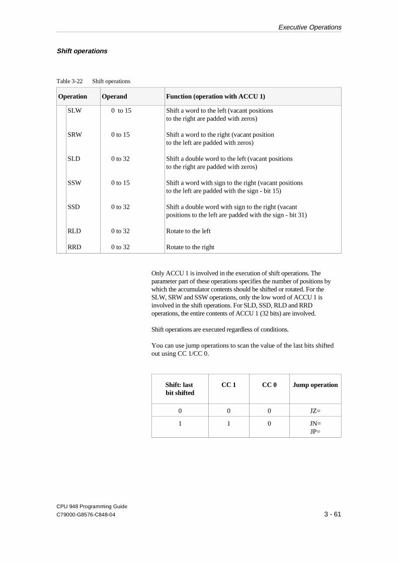
Shift operations
Operation Operand Function (operation with ACCU 1)
SLW
SRW
SLD
SSW
SSD
RLD
RRD
0 to 15
0 to 15
0 to 32
0 to 15
0 to 32
0 to 32
0 to 32
Shift a word to the left (vacant positions to the right are padded with zeros)
Shift a word to the right (vacant position to the left are padded with zeros)
Shift a double word to the left (vacant positionsto the right are padded with zeros)
Shift a word with sign to the right (vacant positionsto the left are padded with the sign - bit 15)
Shift a double word with sign to the right (vacantpositions to the left are padded with the sign - bit 31)
Rotate to the left
Rotate to the right
Only ACCU 1 is involved in the execution of shift operations. Theparameter part of these operations specifies the number of positions bywhich the accumulator contents should be shifted or rotated. For theSLW, SRW and SSW operations, only the low word of ACCU 1 isinvolved in the shift operations. For SLD, SSD, RLD and RRDoperations, the entire contents of ACCU 1 (32 bits) are involved.
Shift operations are executed regardless of conditions.
You can use jump operations to scan the value of the last bits shiftedout using CC 1/CC 0.
Shift: last bit shifted
CC 1 CC 0 Jump operation
0 0 0 JZ=
1 1 0 JN=JP=
Table 3-22 Shift operations
Executive Operations
CPU 948 Programming Guide
C79000-G8576-C848-04 3 - 61
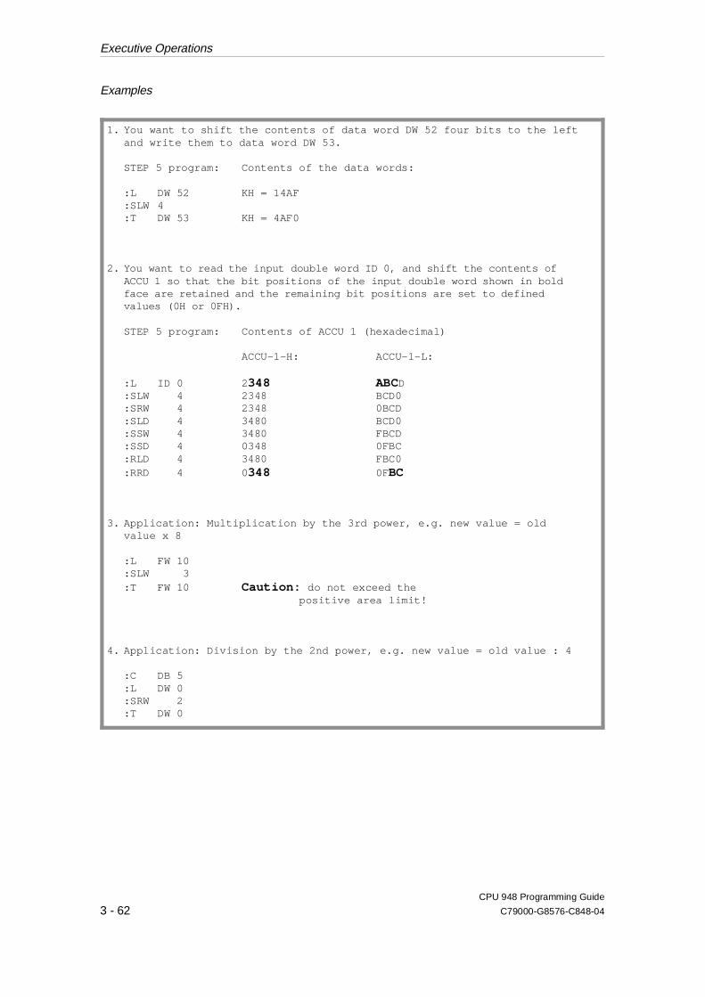
Examples
1. You want to shift the contents of data word DW 52 four bits to the left and write them to data word DW 53.
STEP 5 program: Contents of the data words:
:L DW 52 KH = 14AF:SLW 4:T DW 53 KH = 4AF0
2. You want to read the input double word ID 0, and shift the contents ofACCU 1 so that the bit positions of the input double word shown in bold face are retained and the remaining bit positions are set to defined values (0H or 0FH).
STEP 5 program: Contents of ACCU 1 (hexadecimal)
ACCU-1-H: ACCU-1-L:
:L ID 0 2 348 ABCD:SLW 4 2348 BCD0:SRW 4 2348 0BCD:SLD 4 3480 BCD0:SSW 4 3480 FBCD:SSD 4 0348 0FBC:RLD 4 3480 FBC0:RRD 4 0 348 0FBC
3. Application: Multiplication by the 3rd power, e.g. new value = old value x 8
:L FW 10:SLW 3:T FW 10 Caution: do not exceed the
positive area limit!
4. Application: Division by the 2nd power, e.g. new value = old value : 4
:C DB 5:L DW 0:SRW 2:T DW 0
Executive Operations
CPU 948 Programming Guide
3 - 62 C79000-G8576-C848-04
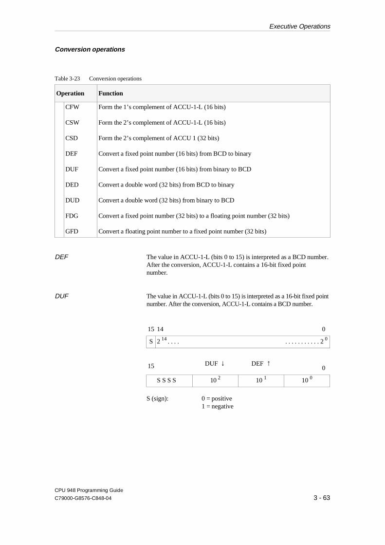
Conversion operations
Operation Function
CFW
CSW
CSD
DEF
DUF
DED
DUD
FDG
GFD
Form the 1’s complement of ACCU-1-L (16 bits)
Form the 2’s complement of ACCU-1-L (16 bits)
Form the 2’s complement of ACCU 1 (32 bits)
Convert a fixed point number (16 bits) from BCD to binary
Convert a fixed point number (16 bits) from binary to BCD
Convert a double word (32 bits) from BCD to binary
Convert a double word (32 bits) from binary to BCD
Convert a fixed point number (32 bits) to a floating point number (32 bits)
Convert a floating point number to a fixed point number (32 bits)
DEF The value in ACCU-1-L (bits 0 to 15) is interpreted as a BCD number.After the conversion, ACCU-1-L contains a 16-bit fixed pointnumber.
DUF The value in ACCU-1-L (bits 0 to 15) is interpreted as a 16-bit fixed pointnumber. After the conversion, ACCU-1-L contains a BCD number.
15 14 0
S 2 14 . . . . . . . . . . . . . . . 2 0
DUF ↓ DEF ↑15 0
S S S S 10 2 10 1 10 0
S (sign): 0 = positive1 = negative
Table 3-23 Conversion operations
Executive Operations
CPU 948 Programming Guide
C79000-G8576-C848-04 3 - 63
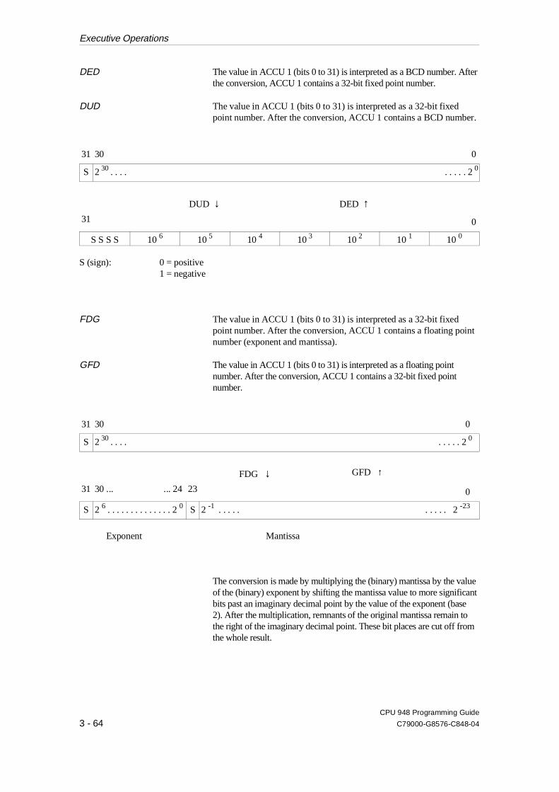
DED The value in ACCU 1 (bits 0 to 31) is interpreted as a BCD number. Afterthe conversion, ACCU 1 contains a 32-bit fixed point number.
DUD The value in ACCU 1 (bits 0 to 31) is interpreted as a 32-bit fixedpoint number. After the conversion, ACCU 1 contains a BCD number.
31 30 0
S 2 30 . . . . . . . . . 2 0
DUD ↓ DED ↑31 0
S S S S 10 6 10 5 10 4 10 3 10 2 10 1 10 0
S (sign): 0 = positive1 = negative
FDG The value in ACCU 1 (bits 0 to 31) is interpreted as a 32-bit fixedpoint number. After the conversion, ACCU 1 contains a floating pointnumber (exponent and mantissa).
GFD The value in ACCU 1 (bits 0 to 31) is interpreted as a floating pointnumber. After the conversion, ACCU 1 contains a 32-bit fixed pointnumber.
31 30 0
S 2 30 . . . . . . . . . 2 0
FDG ↓ GFD ↑
31 30 ... ... 24 23 0
S 2 6 . . . . . . . . . . . . . . 2 0 S 2 -1 . . . . . . . . . . 2 -23
Exponent Mantissa
The conversion is made by multiplying the (binary) mantissa by the valueof the (binary) exponent by shifting the mantissa value to more significantbits past an imaginary decimal point by the value of the exponent (base2). After the multiplication, remnants of the original mantissa remain tothe right of the imaginary decimal point. These bit places are cut off fromthe whole result.
Executive Operations
CPU 948 Programming Guide
3 - 64 C79000-G8576-C848-04

This conversion algorithm produces the following result classes:
•• Floating point numbers ≥ 0 or ≤ -1 result in the next lower number.
•• Floating point numbers < 0 and > -1 result in the value ’0’.
Conversion examples
Examples of CFW, CSW
Floating point number 32-bit fixed point number GFD
+5,7 → 5
-2,3 → -3
-0,6 → 0+0,9 → 0
1. You want the contents of data word DW 64 inverted bit for bit (reversed) and stored in data word DW 78.
STEP 5 program: Assignment of the data words:
:L DW 64 KM = 0011111001011011:CFW:T DW 78 KM = 1100000110100100
2. The contents of data word DW 207 are interpreted as a fixed point number and stored in data word 51 with a reversed sign.
STEP 5 program: Assignment of the data words:
:L DW 207 KF = +51:CSW:T DW 51 KF = -51
Executive Operations
CPU 948 Programming Guide
C79000-G8576-C848-04 3 - 65
Decrement/increment
Operation Operand Function
D
I
1 to 255
1 to 255
Decrement the low byte (bits 0 to 7) of ACCU-1-L by the value of the operand 1)
Increment the low byte (bits 0 to 7) of ACCU-1-Lby the value of the operand 1)
1) The contents of the low byte of ACCU-1-L are decremented or incremented by the number specified as theoperand without a carry. The operation is executed regardless of conditions.
Example
Processing operations
Operation Operand Function
DO
DO =
DW 0 to 255
FW 0 to 254
Process data word:the following operation is combined with the parameter specified in the address data word and executed.
Process flag word:the following operation is combined withthe parameter specified in the addressedF flag and executed.
Process formal operand (parameter type B): Only C DB, JU PB, JU OB, JU FB, JU SB can be substituted.
Insert formal operand
STEP 5 program: Assignment of the data words:
:L DW 7 KH = 1010:I 16:T DW 8 KH = 1020:D 33:T DW 9 KH = 10FF
Table 3-24 Decrement/increment operation
Table 3-25 Processing operations
Executive Operations
CPU 948 Programming Guide
3 - 66 C79000-G8576-C848-04

Operation Operand Function
Table 3-25 continued:
S BI 1) Indirect processing of a formal operand:execute an operation whose operation code is stored in a formal operand. The number of the formal operand must be stored in ACCU 1.
B RS 60 to 63 1) Execute an operation whose operation code is stored in the system data area (RS = free system data: RS 60 to 63). In 2-word operations the 2nd word must be loaded in RS n + 1.
1) The value in the formal operand or system data is interpreted as the operation code of a STEP 5operation and is then executed.
NoteOnly the following operations can be combined with DO DW, orDO FW, DI or DO RS:
- A.. , AN.. , O.. , ON.. , S.. , R.. , =.. with areas I, Q, F, S,
- FR T, R T, SF T, SD T, SP T, SS T, SE T,
- FR C, R C, S C, CD C, CU C,
- L.., T.. with areas P, O, I, Q, F, S, D, RI, RJ, RS, RT,
- L T, L C,
- LC T, LC C,
- JU=, JC=, JZ=, JN=, JP=, JM=, JO=,
- SLW, SRW,
- D, I, SED, SEE,
- C DB, JU.. , JC.., G DB, GX DX, CX DX, DOC FX, DOU FX.
The PG does not check the legality of the combinations!
Executive Operations
CPU 948 Programming Guide
C79000-G8576-C848-04 3 - 67

Examples of DO operations
DO DW/DO FW Operand substitution
Using the statements "DO DW" and "DO FW" you can access data with asubstitution, e.g. in a program loop. The substituted access consists of thestatement DO DW/DO FW followed immediately by one of the STEP 5operations listed above."Substituted" means that the operand for the operation is not programmedas a static value but is fixed during the course of the STEP 5 program.
Select the operand type from the range permitted for the operation whenyou write your program, e.g. PB for the operation "JU PB nn":
You must first load the operand value (nn in the example) in a data wordor F flag word (parameter word) before the substituted access with DO DW/DO FW.
1. Principle of substitution:
:L KF +120:T FW 14 load FW with the value "KF +120":DO FW 14:L IB 0
before the operation "L IB" is executed, theoperand value ’0’ is replaced by the value ’120’;
Operation executed: L IB 120
2. Data word as index register:
The contents of data words DW 20 to DW 100 are set to signal state ’0’. Theindex register for the parameter of the data words is DW 1.
:L KF +20 supply the index register:T DW 1
M001 :L KF +0 reset:DO DW 1:T DW 0:L DW 1 increment the index register:L KF +1:+F:T DW 1:L KF +100:<=F:JC =M001 jump if the index is within the range ... remaining STEP 5 program
Continued on next page
Executive Operations
CPU 948 Programming Guide
3 - 68 C79000-G8576-C848-04
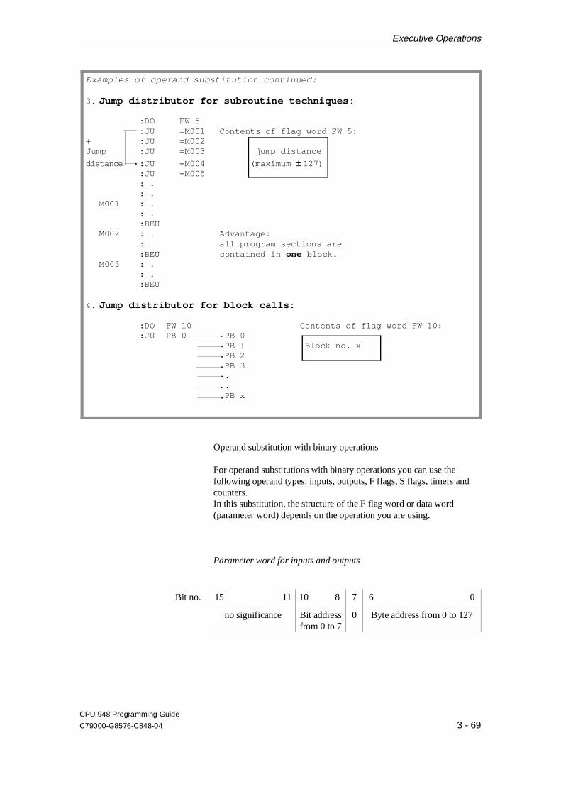
Operand substitution with binary operations
For operand substitutions with binary operations you can use thefollowing operand types: inputs, outputs, F flags, S flags, timers andcounters.In this substitution, the structure of the F flag word or data word(parameter word) depends on the operation you are using.
Parameter word for inputs and outputs
Bit no. 15 11 10 8 7 6 0
no significance Bit addressfrom 0 to 7
0 Byte address from 0 to 127
Examples of operand substitution continued:
3. Jump distributor for subroutine techniques:
:DO FW 5:JU =M001 Contents of flag word FW 5:
+ :JU =M002Jump :JU =M003 jump distance
distance :JU =M004 (maximum ± 127):JU =M005 : .: .
M001 : .: .:BEU
M002 : . Advantage: : . all program sections are:BEU contained in one block.
M003 : .: .:BEU
4. Jump distributor for block calls:
:DO FW 10 Contents of flag word FW 10::JU PB 0 PB 0
PB 1 Block no. x PB 2 PB 3 . . PB x
Executive Operations
CPU 948 Programming Guide
C79000-G8576-C848-04 3 - 69

Parameter word for F flags
Bit no. 15 11 10 8 7 0
no significance Bit addressfrom 0 to 7
Byte address from 0 to 255
Parameter word for S flags
Bit no. 15 14 12 11 0
0 Bit addressfrom 0 to 7
Byte address from 0 to 4095
Parameter word for timers and counters
Bit no. 15 8 7 0
no significance Number of timer orcounter cell from 0 to 255
Principle of the substitutionwith a binary operation
15 8 7 011 10
0 DW 27
DO DW
A I 0.0
27
304
A I 4.30
statement executed
Executive Operations
CPU 948 Programming Guide
3 - 70 C79000-G8576-C848-04
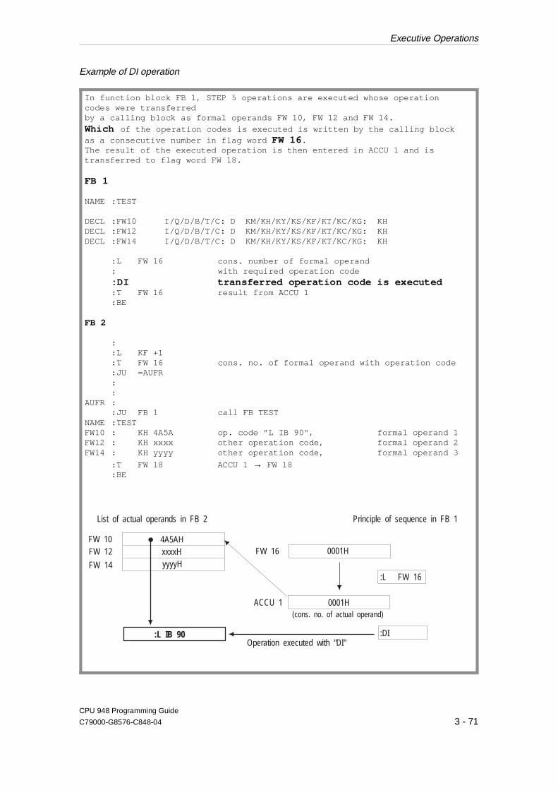
Example of DI operation
In function block FB 1, STEP 5 operations are executed whose operationcodes were transferred by a calling block as formal operands FW 10, FW 12 and FW 14.
Which of the operation codes is executed is written by the calling blockas a consecutive number in flag word FW 16 .The result of the executed operation is then entered in ACCU 1 and istransferred to flag word FW 18.
FB 1
NAME :TEST
DECL :FW10 I/Q/D/B/T/C: D KM/KH/KY/KS/KF/KT/KC/KG: KHDECL :FW12 I/Q/D/B/T/C: D KM/KH/KY/KS/KF/KT/KC/KG: KHDECL :FW14 I/Q/D/B/T/C: D KM/KH/KY/KS/KF/KT/KC/KG: KH
:L FW 16 cons. number of formal operand : with required operation code:DI transferred operation code is executed:T FW 16 result from ACCU 1:BE
FB 2
::L KF +1:T FW 16 cons. no. of formal operand with operation code:JU =AUFR::
AUFR ::JU FB 1 call FB TEST
NAME :TESTFW10 : KH 4A5A op. code "L IB 90", formal operand 1FW12 : KH xxxx other operation code, formal operand 2FW14 : KH yyyy other operation code, formal operand 3
:T FW 18 ACCU 1 → FW 18 :BE
FW 10 4A5AH
:L IB 90
0001H
0001H
List of actual operands in FB 2 Principle of sequence in FB 1
xxxxHyyyyH
Operation executed with "DI"
(cons. no. of actual operand)
FW 12
FW 14
FW 16
ACCU 1
:L FW 16
:DI
Executive Operations
CPU 948 Programming Guide
C79000-G8576-C848-04 3 - 71
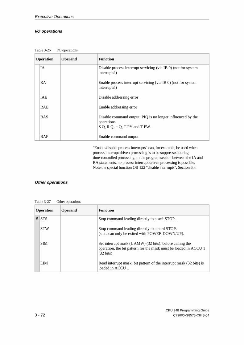
I/O operations
Operation Operand Function
IA
RA
IAE
RAE
BAS
BAF
Disable process interrupt servicing (via IB 0) (not for system interrupts!)
Enable process interrupt servicing (via IB 0) (not for system interrupts!)
Disable addressing error
Enable addressing error
Disable command output: PIQ is no longer influenced by theoperationsS Q, R Q, = Q, T PY and T PW.
Enable command output
"Enable/disable process interrupts" can, for example, be used whenprocess interrupt driven processing is to be suppressed duringtime-controlled processing. In the program section between the IA andRA statements, no process interrupt driven processing is possible.Note the special function OB 122 "disable interrupts", Section 6.3.
Other operations
Operation Operand Function
S STS
STW
SIM
LIM
Stop command leading directly to a soft STOP.
Stop command leading directly to a hard STOP.(state can only be exited with POWER DOWN/UP).
Set interrupt mask (UAMW) (32 bits): before calling theoperation, the bit pattern for the mask must be loaded in ACCU 1(32 bits)
Read interrupt mask: bit pattern of the interrupt mask (32 bits) isloaded in ACCU 1
Table 3-26 I/O operations
Table 3-27 Other operations
Executive Operations
CPU 948 Programming Guide
3 - 72 C79000-G8576-C848-04

SIM/LIM – set/read interruptcondition code mask (UAMW)
The interrupt mask "masks" interrupts in the interrupt condition codeword until the end of the cycle, i.e. all interrupts remain pending, butthe program is not interrupted by them.
Bit in the interrupt condition code mask = 0: interrupt disabledBit in the interrupt condition code mask = 1: interrupt enabled
Meaning of the bits in UAMW-H or ACCU-1-H:
15 8 7 0
INTX INTE INTF INTG WEFE WA PA BULE PEU HALT ES AV INTAS TAU DARY KZU
Meaning of the bits in UAMW-L or ACCU-1-L:
15 8 7 0
– KB KDB STS TLAF SUF STUEBSTUEU NAU ZA QVZ ADF PARE ZYK STOP HOLD
Abbrev. Meaning
High word
INTX
INTEINTFINTGWEFEWAPABULEPEUHALTESAVINTASTAUDARYKZU
S5 bus/system interrupt A, B, C or D (slot-dependent)S5 bus/system interrupt ES5 bus/system interrupt FS5 bus/system interrupt GCollision of timed interruptsTimed interruptProcess interruptBus lock errorI/Os not readyStop instruction from coordinator CORSingle step modeAddress comparison activeInterrupt from SPU processorClock failure of SPU processorContinuous ready (access to faulty memory)Bracket counter overflow
Table 3-28 Meaning of the abbreviations in UAMW
Executive Operations
CPU 948 Programming Guide
C79000-G8576-C848-04 3 - 73
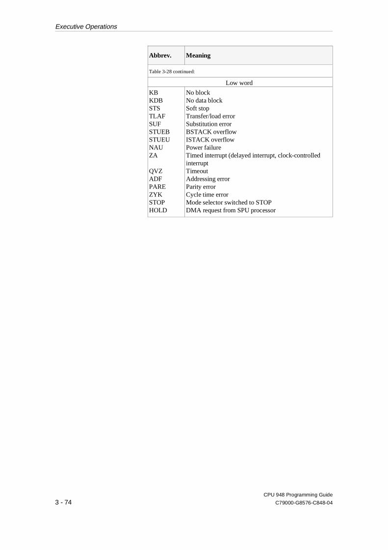
Abbrev. Meaning
Table 3-28 continued:
Low word
KBKDBSTSTLAFSUFSTUEBSTUEUNAUZA
QVZADFPAREZYKSTOPHOLD
No blockNo data blockSoft stopTransfer/load errorSubstitution errorBSTACK overflowISTACK overflowPower failureTimed interrupt (delayed interrupt, clock-controlledinterruptTimeoutAddressing errorParity errorCycle time errorMode selector switched to STOPDMA request from SPU processor
Executive Operations
CPU 948 Programming Guide
3 - 74 C79000-G8576-C848-04
3.5.5Semaphore Operations If two or more CPUs in one programmable controller (see Chapter 10)
require access to the same global memory area (peripherals, CPs, IPs),there is a danger that one CPU will overwrite the data of another CPUor that one CPU could read invalid intermediate data statuses ofanother CPU and misinterpret them. You must therefore coordinateCPU accesses to the common memory areas.
You can coordinate the individual CPUs using the SED and SEEoperations. You can, for example, program the following coordination between twoCPUs: a CPU involved in multiprocessing can only access the commonmemory area after it has successfully set a declared semaphore (SES). Asemaphore xx can only be set by a single CPU. If a CPU fails to set (i.e.disable) the semaphore, it cannot access the memory area. In the sameway, a CPU can no longer access the memory once it has released thesemaphore again (SEE).
SED/SEE disable/enablesemaphore
(non-system operations)
Operation Operand Function
SED
SEE
0 to 31
0 to 31
Disable (set) a semaphore
Enable (release) a semaphore
evaluation of the result of the operation via CC 0/CC 1
NoteThe SED xx and SEE xx operations must be programmed in allCPUs that require synchronized access to a common globalmemory area.
Standard FBs, handling blocks and blocks for multiprocessorcommunication manage the coordination internally. If you usethese blocks, you do not need to program the operations SEE xxand SED xx.
Table 3-29 Disable/enable semaphore
Semaphore Operations
CPU 948 Programming Guide
C79000-G8576-C848-04 3 - 75
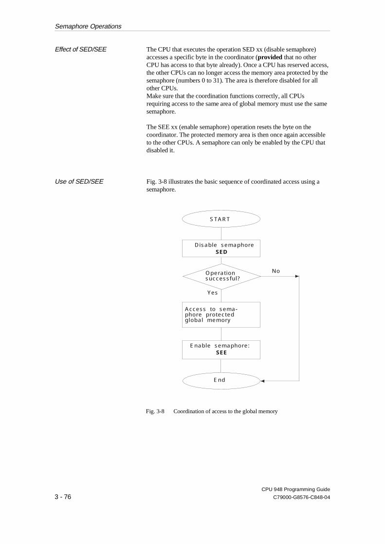
Effect of SED/SEE The CPU that executes the operation SED xx (disable semaphore)accesses a specific byte in the coordinator (provided that no otherCPU has access to that byte already). Once a CPU has reserved access,the other CPUs can no longer access the memory area protected by thesemaphore (numbers 0 to 31). The area is therefore disabled for allother CPUs.Make sure that the coordination functions correctly, all CPUsrequiring access to the same area of global memory must use the samesemaphore.
The SEE xx (enable semaphore) operation resets the byte on thecoordinator. The protected memory area is then once again accessibleto the other CPUs. A semaphore can only be enabled by the CPU thatdisabled it.
Use of SED/SEE Fig. 3-8 illustrates the basic sequence of coordinated access using asemaphore.
START
Operat ionsuccessful?
Disable semaphore
Access to sema-phore protectedglobal memory
Enable semaphore:
No
Yes
End
SED
SEE
Fig. 3-8 Coordination of access to the global memory
Semaphore Operations
CPU 948 Programming Guide
3 - 76 C79000-G8576-C848-04

Before disabling or enabling a particular semaphore, the SED and SEEoperations scan the status of the semaphore. The condition codes CC 0and CC 1 are affected as follows:
CC 1 CC 0 Evaluation Significance
0 0 JZ Semaphore was disabled byanother CPU and cannot bedisabled/enabled.
1 0 JN, JP Semaphore was disabled/enabled.
NoteThe scanning of a particular semaphore (= read procedure) andthe disabling or enabling of the semaphore (=write procedure) areone unit. No other CPU can access the semaphore during theseprocedures!
When using semaphores, remember the following points:
•• A semaphore is a global variable, i.e. the semaphore with number16 exists only once in the entire system, even if your controller isusing three CPUs.
•• All CPUs that require coordinated access to a common memory areamust use the SED and SEE operations.
•• All participating CPUs must execute the same start-up type. Du-ring a COLD RESTART, all the semaphores are cleared. During amanual or automatic warm restart, the semaphores are retained.
•• Start-up in multiprocessor operation must be synchronized. Forthis reason, no test operation is allowed.
Semaphore Operations
CPU 948 Programming Guide
C79000-G8576-C848-04 3 - 77
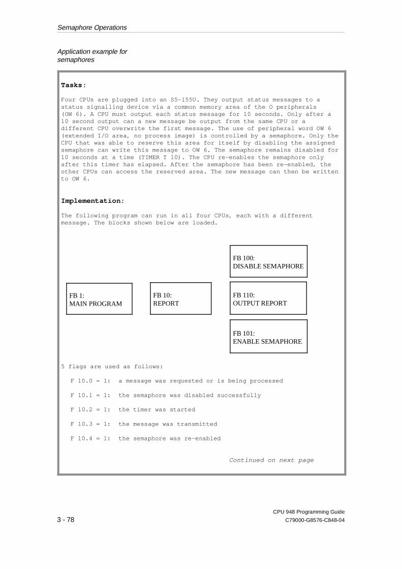
Application example forsemaphores
Tasks:
Four CPUs are plugged into an S5-155U. They output status messages to astatus signalling device via a common memory area of the O peripherals(OW 6). A CPU must output each status message for 10 seconds. Only after a10 second output can a new message be output from the same CPU or adifferent CPU overwrite the first message. The use of peripheral word OW 6(extended I/O area, no process image) is controlled by a semaphore. Only theCPU that was able to reserve this area for itself by disabling the assignedsemaphore can write this message to OW 6. The semaphore remains disabled for10 seconds at a time (TIMER T 10). The CPU re-enables the semaphore onlyafter this timer has elapsed. After the semaphore has been re-enabled, theother CPUs can access the reserved area. The new message can then be writtento OW 6.
Implementation:
The following program can run in all four CPUs, each with a differentmessage. The blocks shown below are loaded.
5 flags are used as follows:
F 10.0 = 1: a message was requested or is being processed
F 10.1 = 1: the semaphore was disabled successfully
F 10.2 = 1: the timer was started
F 10.3 = 1: the message was transmitted
F 10.4 = 1: the semaphore was re-enabled
Continued on next page
FB 1:MAIN PROGRAM
FB 10:REPORT
FB 100:DISABLE SEMAPHORE
FB 110:OUTPUT REPORT
FB 101:ENABLE SEMAPHORE
Semaphore Operations
CPU 948 Programming Guide
3 - 78 C79000-G8576-C848-04

Semaphore application example continued:
FB 1
:A F 10.0:JC =M001 If no message is active,::AN I 0.0:BEC::L KH 2222 generate message and :T FW 12:AN F 10.0:S F 10.0 set "MESSAGE" flag.:
M001 :JU FB10 Call "REPORT" FB NAME :REPORT
::BE
FB 10
NAME :REPORT
:AN F 10.1 If no semaphore is disabled,:JC FB 100 call "disable semaphore" FB.
NAME :SEMADIS::A F 10.1 If the semaphore is disabled:AN F 10.2 and the timer has not started,:S F 10.2:L KT010.2 start the timer.:SE T 10::A F 10.2 If the timer has started :AN F 10.3 and no message is being transmitted,:JC FB 110 call "output message" FB.
NAME :MSGOUT::A F 10.2 If the timer has started:AN F 10.4 and the semaphore is not enabled:AN T 10 and the timer has elapsed, :JC FB 101 call "enable semaphore" FB.
NAME :SEMAENAB::AN F 10.4 If the semaphore is enabled, :BEC::L KH0000:T FY10 reset all flags.:BE
Continued on next page
Semaphore Operations
CPU 948 Programming Guide
C79000-G8576-C848-04 3 - 79
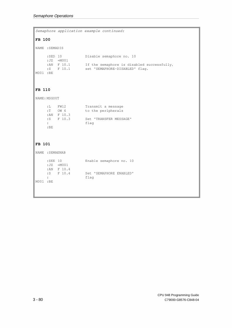
Semaphore application example continued:
FB 100
NAME :SEMADIS
:SED 10 Disable semaphore no. 10 :JZ =M001:AN F 10.1 If the semaphore is disabled successfully,:S F 10.1 set "SEMAPHORE-DISABLED" flag.
M001 :BE
FB 110
NAME: MSGOUT
:L FW12 Transmit a message :T OW 6 to the peripherals:AN F 10.3:S F 10.3 Set "TRANSFER MESSAGE": flag:BE
FB 101
NAME :SEMAENAB
:SEE 10 Enable semaphore no. 10:JZ =M001:AN F 10.4:S F 10.4 Set "SEMAPHORE ENABLED": flag
M001 :BE
Semaphore Operations
CPU 948 Programming Guide
3 - 80 C79000-G8576-C848-04
Contents of Chapter 4
4.1 Program Execution Levels . . . . . . . . . . . . . . . . . . . . . . . . . . . . . . . . . . . . . . . . . . . . . . . . . 4 - 4
4.2 STOP Mode. . . . . . . . . . . . . . . . . . . . . . . . . . . . . . . . . . . . . . . . . . . . . . . . . . . . . . . . . . . . . 4 - 9
4.2.1 SOFT STOP . . . . . . . . . . . . . . . . . . . . . . . . . . . . . . . . . . . . . . . . . . . . . . . . . . . . . . . . . . . . 4 - 94.2.2 HARD STOP . . . . . . . . . . . . . . . . . . . . . . . . . . . . . . . . . . . . . . . . . . . . . . . . . . . . . . . . . . 4 - 134.2.3 OVERALL RESET. . . . . . . . . . . . . . . . . . . . . . . . . . . . . . . . . . . . . . . . . . . . . . . . . . . . . . 4 - 14
4.3 START-UP Mode . . . . . . . . . . . . . . . . . . . . . . . . . . . . . . . . . . . . . . . . . . . . . . . . . . . . . . . 4 - 16
4.3.1 MANUAL and AUTOMATIC COLD RESTART. . . . . . . . . . . . . . . . . . . . . . . . . . . . . . 4 - 174.3.2 MANUAL and AUTOMATIC WARM RESTART . . . . . . . . . . . . . . . . . . . . . . . . . . . . . 4 - 184.3.3 Comparison between COLD RESTART and WARM RESTART. . . . . . . . . . . . . . . . . . 4 - 214.3.4 RETENTIVE COLD RESTART . . . . . . . . . . . . . . . . . . . . . . . . . . . . . . . . . . . . . . . . . . . 4 - 224.3.5 Comparison of COLD RESTART and RETENTIVE COLD RESTART. . . . . . . . . . . . 4 - 234.3.6 User Interfaces for Start-Up . . . . . . . . . . . . . . . . . . . . . . . . . . . . . . . . . . . . . . . . . . . . . . . 4 - 244.3.7 Extended AUTOMATIC WARM RESTART with the CPU 948 (HOT RESTART) . . . 4 - 274.3.8 Interruptions during START-UP . . . . . . . . . . . . . . . . . . . . . . . . . . . . . . . . . . . . . . . . . . . 4 - 28
4.4 RUN Mode . . . . . . . . . . . . . . . . . . . . . . . . . . . . . . . . . . . . . . . . . . . . . . . . . . . . . . . . . . . . 4 - 29
4.4.1 Cyclic Program Execution . . . . . . . . . . . . . . . . . . . . . . . . . . . . . . . . . . . . . . . . . . . . . . . . 4 - 304.4.2 Specifying Time and Interrupt-Driven Program Execution . . . . . . . . . . . . . . . . . . . . . . 4 - 324.4.3 Time-Controlled Program Execution . . . . . . . . . . . . . . . . . . . . . . . . . . . . . . . . . . . . . . . . 4 - 334.4.4 Interrupt-Driven Program Execution . . . . . . . . . . . . . . . . . . . . . . . . . . . . . . . . . . . . . . . . 4 - 41
4Operating Statuses and ProgramExecution Levels
CPU 948 Programming Guide
C79000-G8576-C848-04 4 - 1

Contents
CPU 948 Programming Guide
4 - 2 C79000-G8576-C848-04
4Operating Statuses and ProgramExecution Levels
This chapter provides an overview of the operating statuses andprogram execution levels of the CPU 948. It informs you in detailabout various types of start-up and the organization blocks associatedwith them, in which you can program your own sequences for varioussituations when restarting.
You will also learn the characteristics of the program execution modes"cyclic processing", "time-controlled processing" and"interrupt-driven processing" and will see which blocks are availablefor your user program.
CPU 948 Programming Guide
C79000-G8576-C848-04 4 - 3
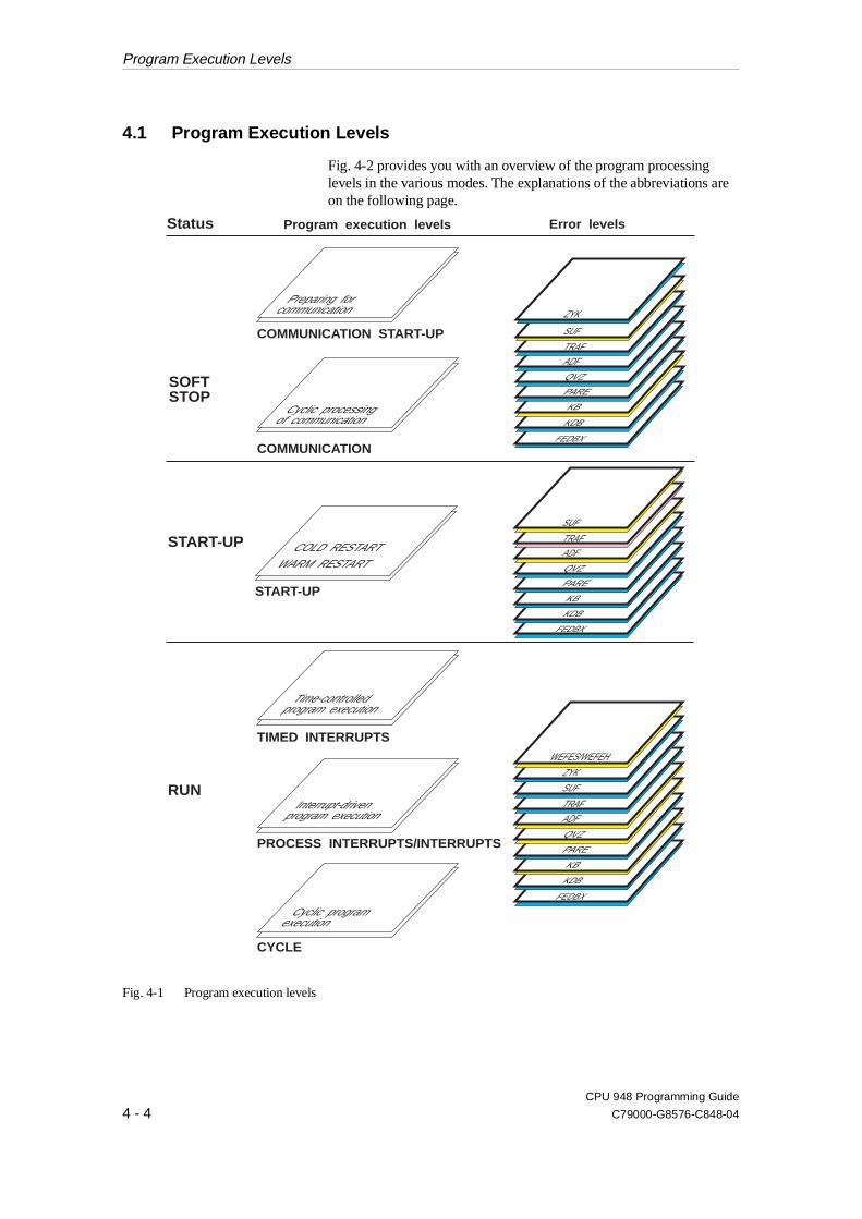
4.1 Program Execution Levels
Fig. 4-2 provides you with an overview of the program processinglevels in the various modes. The explanations of the abbreviations areon the following page.
Error levelsProgram execution levelsStatus
SOFTSTOP
START-UP
RUN
KDBFEDBX
KBPAREQVZADFTRAFSUFZYK
WEFES/WEFEH
FEDBXKDBKB
PAREQVZADFTRAFSUF
COMMUNICATION
Cyclic processingof communication
COMMUNICATION START-UP
Preparing forcommunication
START-UP
WARM RESTARTCOLD RESTART
PROCESS INTERRUPTS/INTERRUPTS
Interrupt-drivenprogram execution
CYCLE
Cyclic programexecution
TIMED INTERRUPTS
Time-controlledprogram execution
FEDBXKDBKB
PAREQVZADFTRAFSUF
ZYK
Fig. 4-1 Program execution levels
Program Execution Levels
CPU 948 Programming Guide
4 - 4 C79000-G8576-C848-04
Level Meaning Priority
Error levels
WEFES/WEFEHZYKSUFTRAFADFQVZPAREKBKDBFEDBX
Collision of timed interruptsCycle errorSubstitution errorTransfer/load errorAddressing errorTimeoutParity errorCalled code block does not existCalled data block does not existError generating a data block, DB or DX
Each error handlingroutine has the highestpriority. If an erroroccurs, thecorresponding errorlevel is nested inimmediately.
Program execution levels in SOFT STOP
COMMUNICATION START-UPCOMMUNICATION
Preparation (start-up) for communicationCyclic processing of communication
–
Program processing levels in START-UP
COLD RESTART
WARM RESTART
Defined start of the user program
Continuation of the user program at thepoint of interruption
–
Program execution levels in RUN
TIMED INTERRUPTSPROCESS INTERRUPTSCYCLE
Time-controlled program executionInterrupt-driven program executionCyclic program execution
Ascending 1)
priority(default)
1) The default can be changed by selecting parameters for DX 0 (refer to Chapter 7).
Processing via the systemprogram
A specific system program is responsible for each level.
Interrupt stack (ISTACK) If an interrupt occurs, the system program sets up an information fieldin the ISTACK for each level, to allow it to continue in the interruptedlevel after servicing the interrupt.
Table 4-1 Program execution levels
Program Execution Levels
CPU 948 Programming Guide
C79000-G8576-C848-04 4 - 5
Nesting other levels When an event occurs, which requires higher priority processing, thecurrent level is interrupted by the system program and the higherpriority level is activated.
This occurs in the following situations:
•• at error levels: always at operation boundaries,
•• all other levels: at block or operation boundaries(depending on the setting in DX 0 refer to Chapter 7)
NoteA maximum of 5 error organization blocks can be nested. If 5error levels are activated simultaneously, this causes an ISTACKoverflow and the CPU changes to the HARD STOP.
A specific program execution level is assigned to one or a group oforganization blocks which are called by the system program after anevent. If, for example, OB 9 is called to process a time-controlledinterrupt, the program execution level TIMED INTERRUPTS isactivated.
After the system program calls an organization block, the CPUexecutes the STEP 5 statements is contains. The current registerrecord is saved in the ISTACK and a new register record is set up(register: ACCU 1 to 4, block stack pointer, block address register,data block start address, data block length, step address counter, baseaddress register and the interrupt condition code words ICMK andICRW).If "normal" program execution is interrupted by the occurrence of anevent, following the execution of the OB, the CPU continues theprogram execution at the point of interruption (including all the blocksnested there) as long as no stop is programmed in the OB.
Program Execution Levels
CPU 948 Programming Guide
4 - 6 C79000-G8576-C848-04

Sub-levels The TIMED INTERRUPTS level contains several sub-levels to whicha specific program (OB) is assigned. Within the TIMEDINTERRUPTS level, the sub-levels have their own priority (refer tothe following table).
TIMED INTERRUPTS level
Sub-level Priority
Delayed interruptcyclic timed interrupt, shortest period......cyclic timed interrupt, longest periodtime-driven interrupt
ascendingpriority(default)
Examples
Example of"Execution by the system program":
At the CYCLE program execution level, the system program updates theprocess image of the inputs and outputs, triggers the cycle monitoring timeand calls the PG interface management (system checkpoint).
Program Execution Levels
CPU 948 Programming Guide
C79000-G8576-C848-04 4 - 7
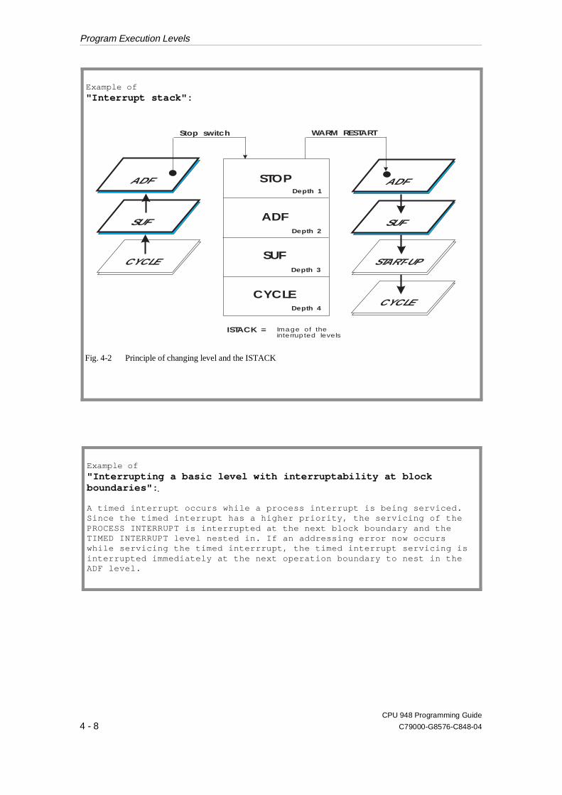
Example of"Interrupt stack":
CYCLE START-UP
CYCLE
SUF SUF
ADFADF
ADF
STOP
SUF
CYCLE
Depth 3
Depth 4
Depth 2
Depth 1
ISTACK = Image of theinterrupted levels
Stop switch WARM RESTART
Fig. 4-2 Principle of changing level and the ISTACK
Example of"Interrupting a basic level with interruptability at blockboundaries":
A timed interrupt occurs while a process interrupt is being serviced.Since the timed interrupt has a higher priority, the servicing of thePROCESS INTERRUPT is interrupted at the next block boundary and theTIMED INTERRUPT level nested in. If an addressing error now occurswhile servicing the timed interrrupt, the timed interrupt servicing isinterrupted immediately at the next operation boundary to nest in theADF level.
Program Execution Levels
CPU 948 Programming Guide
4 - 8 C79000-G8576-C848-04
4.2 STOP Mode
The CPU 948 has two different STOP modes, the "hard" STOP andthe "soft" STOP (= CPU capable of communication).
4.2.1SOFT STOP The SOFT STOP mode has the following features:
The CPU can communicate: the system program calls organizationblock OB 38 once after POWER UP (COMMUNICATIONSTART-UP level in SOFT STOP) and then calls OB 39(COMMUNICATION level in SOFT STOP).
Initialization of communication (OB 38)
To initialize communication, the system program calls OB 38 as theuser interface.
OB 38 is only called after POWER UP . The call is notdependent on the type of start-up (AUTOMATIC COLD/AUTOMATIC WARM RESTART) set in data block DX 0.
Start-up monitoring of OB 38
The time required for the execution of OB 38 is not monitored by thesystem program. You can, however, abort execution by changing themode selector to STOP.
If an error occurs in OB 38, its execution is aborted and OB 39 iscalled if it exists.
Cyclic communication (OB 39)
If the cyclic program is interrupted causing a change to the SOFTSTOP mode, OB 39 is called as the user interface.
If the interruption of the cyclic program means that a handling block(communication) is not completely executed, it is possible andpermitted to re-call the same block or the same block type in OB 39(e.g. SEND).
STOP Mode
CPU 948 Programming Guide
C79000-G8576-C848-04 4 - 9
Monitoring the executiontime of OB 39
The execution time of OB 39 is monitored by the system program. Ifexecution takes longer than 2.55 seconds (fixed value), the systemprogram detects a cycle time error; it then calls the error OB, OB 26,and then processes OB 39 again from the beginning. If a cycle timeerror occurs again, an ISTACK depth > 5 causes an ISTACK overflow(reaction: see following paragraph).
Reaction to anerror in OB 39
If an error occurs in OB 39 or in a handling block called in OB 39(e.g. QVZ), the system program calls the appropriate errororganization block. After this has been executed, the programprocessing is continued in OB 39. If the error OB does not exist,OB 39 is executed again from the beginning. (Exception: with QVZ,KB and errors in the self test there is no reaction).If further errors occur, an ISTACK depth > 5 causes an ISTACKoverflow:the system program aborts program execution (OB 39 is no longercalled), the CPU however remains in the SOFT STOP mode.
Data are not reset If cyclic execution has already taken place in the RUN mode, thevalues of counters, timers, flags and the process image are retainedduring the transition to the stop mode.
Real-time clock The real-time clock continues to run. It is updated in the RS area at10 ms intervals.
BASP signal The BASP (disable output command) signal is active. This disables allthe digital outputs (exception: in the test in multiprocessor operationand with the PG function "force outputs", BASP is not active - refer toSection 10.1.8).
ISTACK If a user program was processed prior to the stop mode, information isentered in the interrupt stack (ISTACK) providing information aboutthe cause of the interruption.
Timer processing in OB 38/39 While OB 38/39 is being executed, the processing of timers andcounters is stopped. If necessary, timer information must beprocessed from system data area RS 96 to RS 99 or with OB 121or OB 150.
STOP Mode
CPU 948 Programming Guide
4 - 10 C79000-G8576-C848-04
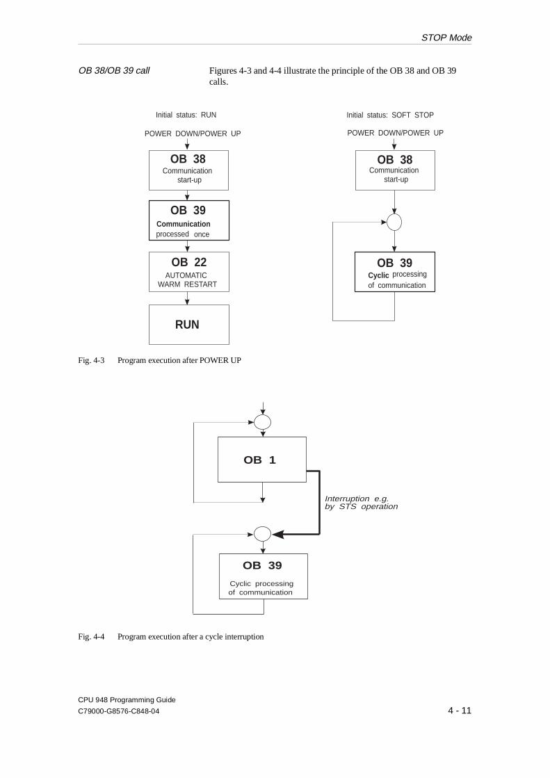
OB 38/OB 39 call Figures 4-3 and 4-4 illustrate the principle of the OB 38 and OB 39calls.
OB 38OB 38
OB 39
OB 22
RUN
OB 39
Communicationstart-up
Communicationstart-up
Initial status: RUN Initial status: SOFT STOP
POWER DOWN/POWER UPPOWER DOWN/POWER UP
Communicationprocessed once
AUTOMATICWARM RESTART
Cyclic processingof communication
Fig. 4-3 Program execution after POWER UP
OB 1
OB 39
Interruption e.g.by STS operation
Cyclic processingof communication
Fig. 4-4 Program execution after a cycle interruption
STOP Mode
CPU 948 Programming Guide
C79000-G8576-C848-04 4 - 11

LED displays The SOFT STOP status can be recognized by the LEDs on the frontpanel of the CPU as follows:
LED Status
RUN off
STOP on (continuous or flashing light)
SYSFAULT off
BASP on (except in test mode with multiprocessor modeor with PG function "force outputs")
The STOP LED signals the possible causes of the current stop status,as follows:
STOP LED lit continuously The SOFT STOP mode was triggered by the following:
in single processor operation:- by changing the mode selector
from RUN to STOP,- by the PG function PLC STOP,- by a device fault (PEU),- following an OVERALL RESET.
in multiprocessor operation:- by changing the mode selector on the COR to STOP,- a different CPU has changed to the STOP mode due to a problem
(each CPU not causing the error has a constantly lit LED) or by the STOP switch,
- PG function PLC STOP- PG function "program test end" on a different CPU
STOP LED flashes slowly(approx. once every 2 sec)
The SOFT STOP was triggered by the following:
- STP or STS statement in the user program,- operator error (DB 1/DX 0 error, selection of an illegal start-up
mode etc.),- BSTACK overflow (STUEB) or bracket counter overflow (KZU),- programming errors or device faults; the following LEDs provide
further information:- "ADF" LED- "QVZ" LED- "ZYK" LED
- by the PG function "program test end" on this CPU.
STOP Mode
CPU 948 Programming Guide
4 - 12 C79000-G8576-C848-04
Exiting the SOFT STOP status
The SOFT STOP status can be exited as follows:
a) by selecting a restart (refer to Section 4.4),
b) by an OVERALL RESET followed by a COLD RESTART.
4.2.2HARD STOP If the system program can no longer be executed properly, the CPU
changes to the HARD STOP mode to ensure a safe mode in thissituation.
A HARD STOP can be caused by the following:
•• stop operation (STW) for the system program
•• ISTACK overflow (STUEU),
•• timeout (QVZ) or parity error (PARE) in the systemRAM/EPROM,
•• error in system program
NoteThe CPU is stopped. You can only exit the HARD STOP modeby switching the power off and then on again!
LED displays The HARD STOP status can be recognized by the following LEDs onthe front panel of the CPU:
LED Status
RUN off
STOP off
SYSFAULT on
BASP on
STOP Mode
CPU 948 Programming Guide
C79000-G8576-C848-04 4 - 13
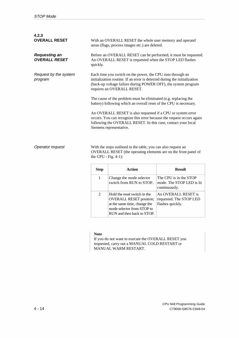
4.2.3OVERALL RESET With an OVERALL RESET the whole user memory and operand
areas (flags, process images etc.) are deleted.
Requesting an OVERALL RESET
Before an OVERALL RESET can be performed, it must be requested.An OVERALL RESET is requested when the STOP LED flashesquickly.
Request by the systemprogram
Each time you switch on the power, the CPU runs through aninitialization routine. If an error is detected during the initialization(back-up voltage failure during POWER OFF), the system programrequires an OVERALL RESET.
The cause of the problem must be eliminated (e.g. replacing thebattery) following which an overall reset of the CPU is necessary.
An OVERALL RESET is also requested if a CPU or system erroroccurs. You can recognize this error because the request occurs againfollowing the OVERALL RESET. In this case, contact your localSiemens representative.
Operator request With the steps outlined in the table, you can also request anOVERALL RESET (the operating elements are on the front panel ofthe CPU - Fig. 4-1):
Step Action Result
1 Change the mode selectorswitch from RUN to STOP.
The CPU is in the STOPmode. The STOP LED is litcontinuously.
2 Hold the reset switch in theOVERALL RESET position;at the same time, change themode selector from STOP toRUN and then back to STOP.
An OVERALL RESET isrequested. The STOP LEDflashes quickly.
NoteIf you do not want to execute the OVERALL RESET yourequested, carry out a MANUAL COLD RESTART orMANUAL WARM RESTART.
STOP Mode
CPU 948 Programming Guide
4 - 14 C79000-G8576-C848-04
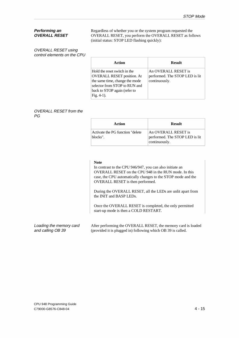
Performing an OVERALL RESET
Regardless of whether you or the system program requested theOVERALL RESET, you perform the OVERALL RESET as follows(initial status: STOP LED flashing quickly):
OVERALL RESET usingcontrol elements on the CPU
Action Result
Hold the reset switch in theOVERALL RESET position. Atthe same time, change the modeselector from STOP to RUN andback to STOP again (refer toFig. 4-1).
An OVERALL RESET isperformed. The STOP LED is litcontinuously.
OVERALL RESET from thePG
Action Result
Activate the PG function "deleteblocks".
An OVERALL RESET isperformed. The STOP LED is litcontinuously.
NoteIn contrast to the CPU 946/947, you can also initiate anOVERALL RESET on the CPU 948 in the RUN mode. In thiscase, the CPU automatically changes to the STOP mode and theOVERALL RESET is then performed.
During the OVERALL RESET, all the LEDs are unlit apart fromthe INIT and BASP LEDs.
Once the OVERALL RESET is completed, the only permittedstart-up mode is then a COLD RESTART.
Loading the memory card and calling OB 39
After performing the OVERALL RESET, the memory card is loaded(provided it is plugged in) following which OB 39 is called.
STOP Mode
CPU 948 Programming Guide
C79000-G8576-C848-04 4 - 15

4.3 START-UP Mode
The START-UP mode has the following features:
Mode change START-UP is the transition from the STOP mode to the RUN mode.
Start-up types The CPU 948 has the following start-up modes:
- COLD RESTART ( manual or automatic)- WARM RESTART (manual or automatic)(You can select the type of start-up with operating elements and byassigning parameters in DX 0)
COLD RESTART The cyclic user program is processed from the beginning.
The system program calls OB 20 as the user interface.
WARM RESTART The execution of the cyclic user program is continued from the pointat which it was interrupted.
The system program calls the following OBs as the user interface:
- OB 21 for a MANUAL WARM RESTART,- OB 22 for an AUTOMATIC WARM RESTART.
No time monitoring of thestart-up OBs
The execution time of the start-up organization blocks is notmonitored. You can call other blocks within these OBs. Make sureyou avoid endless loops!
Counters, timers, flags,process images
The values of counters, timers, flags and process images are handleddifferently in the various start-up types (refer to Section 4.4.3).
BASP The BASP signal (disable output command) is active. This disables allthe digital outputs (exception: in the test mode in multiprocessoroperation, the BASP is not activated - refer to Section 10.1.8).
Interrupts The interrupts (normal interrupts, process interrupts, timed interrupts)are disabled.
Start-up in the multiprocessormode
Starting up in the multiprocessor mode is described in Section 10.1.7.
START-UP Mode
CPU 948 Programming Guide
4 - 16 C79000-G8576-C848-04
4.3.1MANUAL and AUTOMATIC COLD RESTART
When is a COLD RESTARTpermitted?
A COLD RESTART is always permitted provided the system is notrequesting an OVERALL RESET.
When is a COLD RESTARTnecessary?
A COLD RESTART is necessary after the following:
- OVERALL RESET,- loading the user memory with the user program while the CPU
is in the stop mode- ISTACK/BSTACK overflow,- COLD RESTART aborted (by POWER OFF or changing the
mode selector to "STOP"),- stop after PG function "program test end"
MANUAL COLD RESTART You can trigger a MANUAL COLD RESTART as follows:
•• Using the operating elements of the CPU:
Hold the reset switch in the RESET position; at the same time changethe mode selector from STOP to RUN (refer to Fig. 4-1).
•• From the PG:
Select the PG function PLC START/COLD RESTART.
AUTOMATIC COLDRESTART
An AUTOMATIC COLD RESTART is triggered as follows:
At POWER UP, when
- the default "AUTOMATIC WARM RESTART after POWER UP"in DX 0 has been changed to "AUTOMATIC COLD RESTART after POWER UP",
- the mode selector on all CPUs and on the coordinator must remainset to RUN and the CPU was not in the STOP mode when the power was switched off.
NoteIf the CPU was in the STOP mode when the power was switchedoff (for example, following an addressing error), anAUTOMATIC COLD RESTART is not permitted. The STOPmode can only be exited in this case with a MANUAL COLDRESTART.
START-UP Mode
CPU 948 Programming Guide
C79000-G8576-C848-04 4 - 17
Aborting a cold restart You can abort an active COLD RESTART only by changing the modeselector to STOP or by switching off the power. If you abort a COLDRESTART you must repeat it.
4.3.2MANUAL and AUTOMATIC WARM RESTART
When is a WARM RESTARTpossible and permitted?
A MANUAL WARM RESTART is only possible after stoppagescaused by the following:
•• the mode selector was changed from the RUN position to theSTOP position,
•• a stoppage in multiprocessor operation caused by the HALT signalfrom the coordinator,
•• POWER OFF, with the appropriate setting in data block DX 0,
•• PG function PLC STOP.
NoteIf the stoppage was caused by an event other than those listedabove, then no warm restart is possible. The system programwill only permit a COLD RESTART.
A MANUAL or AUTOMATIC WARM RESTART is onlypermitted when
•• the user program was not modified during the stop mode
and
•• a COLD RESTART is not necessary for other reasons (refer toSection 4.4.1).
START-UP Mode
CPU 948 Programming Guide
4 - 18 C79000-G8576-C848-04

MANUAL WARM RESTART You trigger a MANUAL WARM RESTART as follows:
•• using the control elements of the CPU:
initial state: the reset switch is in the mid setting
change the mode selector from STOP to RUN (refer to Fig. 4-1)
•• from the PG:
select the PG function PLC START/WARM RESTART.
AUTOMATIC WARMRESTART
An AUTOMATIC WARM RESTART is triggered as follows:
With POWER UP, when
- the default "AUTOMATIC WARM RESTART after POWER UP"is set in data block DX 0 or DX 0 does not exist,
- the mode selector on all CPUs and on the coordinator remainunchanged and set to RUNand the CPU was not in the STOP mode when the power was switched off,
- no further errors have occurred during the initialization nor beforethe power was switched off,
- no COLD RESTART is required due to the reasons listed above.
Following power failure or switching the power off in the RUN modefollowed by the return of power/POWER UP, the CPU runs throughan initialization routine and then automatically performs a WARMRESTART.
If there is a power failure on an expansion unit, (PEU signal), the CPUchanges to the STOP mode. It remains in this mode until the PEUsignal is switched inactive and then performs an AUTOMATICWARM RESTART or an AUTOMATIC COLD RESTART.
START-UP Mode
CPU 948 Programming Guide
C79000-G8576-C848-04 4 - 19

NoteWith a WARM RESTART note the following special situation:
The CPU is currently processing an error OB (e.g. due to anaddressing error ADF) and then changes to the STOP modeowing to POWER OFF, HALT, stop switch or PG-STP.Following this, a MANUAL or AUTOMATIC WARMRESTART is executed.
Reaction of the CPU:
- Before OB 21/22 is called, the interrupted processing of the error OB is completed.
- If the error OB does not lead to a stop operation, then followingthe processing of the remainder of the error OB, a WARMRESTART is executed.
- If the error OB sets the CPU to the stop mode, then only aCOLD RESTART is possible.
Aborting aWARM RESTART
You can only abort a WARM RESTART after it has started bychanging the mode selector to STOP or by POWER OFF. If you abortthe warm restart in this way, both a COLD RESTART or WARMRESTART is then possible.
START-UP Mode
CPU 948 Programming Guide
4 - 20 C79000-G8576-C848-04
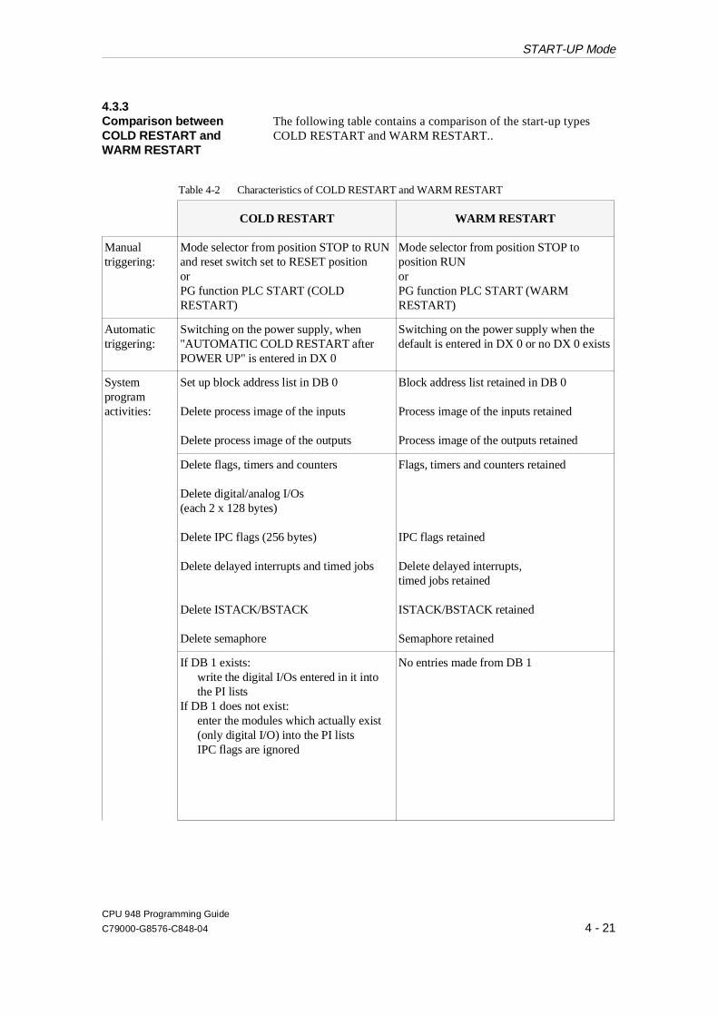
4.3.3Comparison betweenCOLD RESTART and WARM RESTART
The following table contains a comparison of the start-up typesCOLD RESTART and WARM RESTART..
COLD RESTART WARM RESTART
Manualtriggering:
Mode selector from position STOP to RUNand reset switch set to RESET positionorPG function PLC START (COLDRESTART)
Mode selector from position STOP toposition RUNorPG function PLC START (WARMRESTART)
Automatictriggering:
Switching on the power supply, when"AUTOMATIC COLD RESTART afterPOWER UP" is entered in DX 0
Switching on the power supply when thedefault is entered in DX 0 or no DX 0 exists
Systemprogramactivities:
Set up block address list in DB 0
Delete process image of the inputs
Delete process image of the outputs
Block address list retained in DB 0
Process image of the inputs retained
Process image of the outputs retained
Delete flags, timers and counters
Delete digital/analog I/Os (each 2 x 128 bytes)
Delete IPC flags (256 bytes)
Delete delayed interrupts and timed jobs
Delete ISTACK/BSTACK
Delete semaphore
Flags, timers and counters retained
IPC flags retained
Delete delayed interrupts,timed jobs retained
ISTACK/BSTACK retained
Semaphore retained
If DB 1 exists:write the digital I/Os entered in it intothe PI lists
If DB 1 does not exist:enter the modules which actually exist(only digital I/O) into the PI listsIPC flags are ignored
No entries made from DB 1
Table 4-2 Characteristics of COLD RESTART and WARM RESTART
START-UP Mode
CPU 948 Programming Guide
C79000-G8576-C848-04 4 - 21
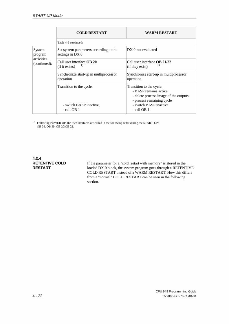
COLD RESTART WARM RESTART
Table 4-3 continued:
Systemprogramactivities(continued):
Set system parameters according to thesettings in DX 0
DX 0 not evaluated
Call user interface OB 20 (if it exists) 1)
Call user interface OB 21/22 (if they exist) 1)
Synchronize start-up in multiprocessoroperation
Synchronize start-up in multiprocessoroperation
Transition to the cycle:
- switch BASP inactive,- call OB 1
Transition to the cycle:- BASP remains active- delete process image of the outputs- process remaining cycle- switch BASP inactive- call OB 1
1) Following POWER UP, the user interfaces are called in the following order during the START-UP:OB 38, OB 39, OB 20/OB 22.
4.3.4RETENTIVE COLD RESTART
If the parameter for a "cold restart with memory" is stored in theloaded DX 0 block, the system program goes through a RETENTIVECOLD RESTART instead of a WARM RESTART. How this differsfrom a "normal" COLD RESTART can be seen in the followingsection.
START-UP Mode
CPU 948 Programming Guide
4 - 22 C79000-G8576-C848-04
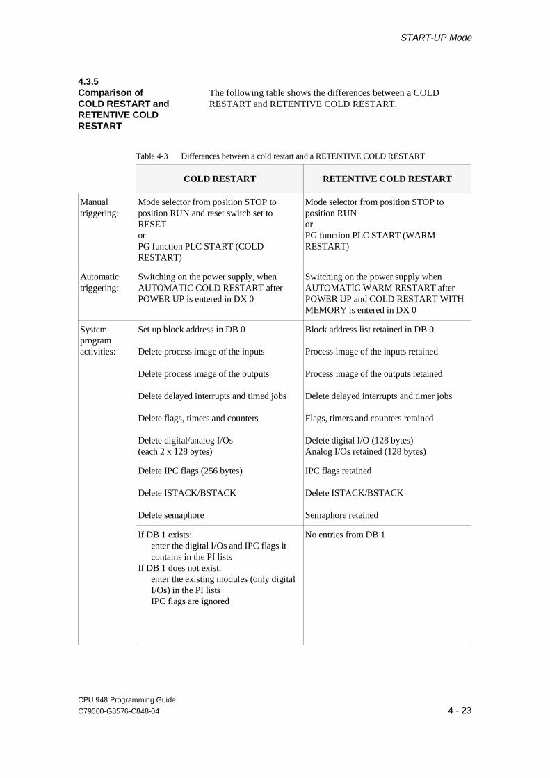
4.3.5Comparison of COLD RESTART and RETENTIVE COLD RESTART
The following table shows the differences between a COLDRESTART and RETENTIVE COLD RESTART.
COLD RESTART RETENTIVE COLD RESTART
Manualtriggering:
Mode selector from position STOP toposition RUN and reset switch set toRESETorPG function PLC START (COLDRESTART)
Mode selector from position STOP toposition RUN orPG function PLC START (WARMRESTART)
Automatictriggering:
Switching on the power supply, whenAUTOMATIC COLD RESTART afterPOWER UP is entered in DX 0
Switching on the power supply whenAUTOMATIC WARM RESTART afterPOWER UP and COLD RESTART WITHMEMORY is entered in DX 0
Systemprogramactivities:
Set up block address in DB 0
Delete process image of the inputs
Delete process image of the outputs
Delete delayed interrupts and timed jobs
Delete flags, timers and counters
Delete digital/analog I/Os (each 2 x 128 bytes)
Block address list retained in DB 0
Process image of the inputs retained
Process image of the outputs retained
Delete delayed interrupts and timer jobs
Flags, timers and counters retained
Delete digital I/O (128 bytes)Analog I/Os retained (128 bytes)
Delete IPC flags (256 bytes)
Delete ISTACK/BSTACK
Delete semaphore
IPC flags retained
Delete ISTACK/BSTACK
Semaphore retained
If DB 1 exists:enter the digital I/Os and IPC flags it contains in the PI lists
If DB 1 does not exist:enter the existing modules (only digitalI/Os) in the PI listsIPC flags are ignored
No entries from DB 1
Table 4-3 Differences between a cold restart and a RETENTIVE COLD RESTART
START-UP Mode
CPU 948 Programming Guide
C79000-G8576-C848-04 4 - 23

COLD RESTART RETENTIVE COLD RESTART
Systemprogramactivities(continued)
Table 4-4 continued:
Set system parameters according to defaultin DX 0
No evaluation of DX 0
Call user interface OB 20 (if it exists) 1)
Call user interface OB 21/22(if it exists) 1)
Synchronize start-up in multiprocessoroperation
Synchronize start-up in multiprocessoroperation
Transition to the cycle:
- switch BASP inactive- call OB 1
Transition to the cycle:
- switch BASP inactive- call OB 1
1) After POWER ON, the user interfaces are called in the following order during START-UP:OB 38, OB 39, OB 20/OB 22.
4.3.6User Interfaces for Start-Up The organization blocks OB 20, OB 21 and OB 22 serve as user
interfaces for the various types of start-up. You can store your STEP 5program for the type of start-up in these blocks.
OB 20 When the CPU executes a MANUAL or AUTOMATIC COLDRESTART, the system program calls OB 20 once. In OB 20, you canstore a STEP 5 program which is responsible for preliminary steps fora cold restart of cyclic processing prior to the execution of the cyclicprogram.
You can, for example:
•• set flags
•• start timers (the start is executed by the system program when it en-ters the RUN mode)
•• set default values for data to be output to I/O modules
•• synchronize CPs.
After processing OB 20, the cyclic program begins by calling OB 1.If OB 20 is not loaded, the CPU begins the cyclic programexecution immediately after the COLD RESTART is completed(following the system activities).
START-UP Mode
CPU 948 Programming Guide
4 - 24 C79000-G8576-C848-04
OB 21 If the CPU performs a MANUAL COLD RESTART or RETENTIVEMANUAL COLD RESTART, the system program calls OB 21 once.Here, you can store a STEP 5 program which executes preliminarysteps for a warm restart of the cyclic program.
MANUAL WARM RESTART With a MANUAL WARM RESTART, the cyclic program iscontinued with the next statement following the point at which it wasinterrupted after processing OB 21, the sequence is as follows:
•• The BASP signal (disable command output) remains active duringthe processing of the remaining cycle and is only switched inactiveat the beginning of the next (complete) cycle.
•• The process image of the outputs is reset at the end of theremaining cycle.
•• If OB 21 is not loaded, the CPU begins again at the point at whichthe program was interrupted on completion of the MANUALWARM RESTART and the system activities.
MANUAL RETENTIVE COLDRESTART
If the parameter "COLD RESTART WITH MEMORY" is entered inthe data block DX 0, after processing OB 21, the system program thengoes through a COLD RESTART (the CPU resumes programexecution with the first STEP 5 statement in OB 1). The signalstates of the flags, IPC flags, semaphore and the block address list(DB 0) are retained.
START-UP Mode
CPU 948 Programming Guide
C79000-G8576-C848-04 4 - 25
OB 22 When the CPU executes an AUTOMATIC WARM RESTART orAUTOMATIC RETENTIVE COLD RESTART, the system programcalls OB 22 once. Here, you can store a STEP 5 program whichexecutes preliminary steps (generally following a power failure) for awarm restart of cyclic program execution.
AUTOMATIC WARMRESTART
Following POWER UP, the CPU executes the system activities listedin Section 4.4.4 for a warm restart and attempts to resume the programat the point at which it was interrupted.
OB 22 is called first.
After executing OB 22, the interrupted program execution is resumedwith the next statement following the point at which the program wasinterrupted.
Following a power failure and the return of power:
•• The BASP signal (disable command output) remains active duringthe remaining cycle and is only switched inactive at the beginningof the first complete cycle.
•• The process image of the outputs is reset at the end of theremaining cycle.
•• If OB 22 is not loaded, the CPU resumes program processingimmediately at the point of interruption at the end of theAUTOMATIC WARM RESTART.
AUTOMATIC RETENTIVECOLD RESTART
If the parameter "COLD RESTART WITH MEMORY" is entered inthe data block DX 0, after processing OB 22, the system program thengoes through a COLD RESTART (the CPU resumes programexecution with the first STEP 5 statement in OB 1). The signalstates of the flags, IPC flags, semaphore and the block address list(DB 0) are retained.
START-UP Mode
CPU 948 Programming Guide
4 - 26 C79000-G8576-C848-04
4.3.7Extended AUTOMATICWARM RESTART with theCPU 948 (HOT RESTART)
The "HOT RESTART" mode specified in the IEC 1131 standard, part1 is also possible in the CPU 948. The "HOT RESTART" is a warmrestart controlled by a battery-backed clock (according to IEC 1131).The clock monitors the time between switching off and switching onthe power supply for the CPU. Whether or not a warm restart is thenpermitted depends on the time elapsed.
The automatic "HOT RESTART" of the CPU 948 is not supporteddirectly by the system program, which means that you must programthis yourself.
The basic functions available are the AUTOMATIC WARMRESTART (OB 22) and the real time clock which although internal isbacked up by an external battery.
A "HOT RESTART" is programmed as shown below:
Mode Activity/block
RUN Save time (time of day and date) regularly from the external clock in defined memorycells (e.g. in data words):
- at the end of the cycle in OB 1
or
- time-controlled by timed interrupts (e.g. OB 10), if higher accuracy is necessary
AUTO-MATICWARMRESTART
OB 22
Calculate down time:Tdown = first time value after return of power - last time value saved before power failure
IF ... THEN...
Down time > default maximum value Stop warm restart (STP operation)
or
execute modified warm restart
Down time ≤ default maximum value Continue warm restart
START-UP Mode
CPU 948 Programming Guide
C79000-G8576-C848-04 4 - 27

4.3.8Interruptions during START-UP
A start-up program can be interrupted by the following: •• power failure in the central controller (NAU) or in the expansion
unit (PEU),•• stop switch, stop command, HALT or PG-STPor•• program errors or device faults (refer to Section 5.5).
Basic rules for an interruptedSTART-UP
The following basic rules apply to the start-up response of theCPU 948:
If the START-UP is interrupted, the subsequent START-UP isalways restarted from the beginning.
The last selected type of start-up is selected. Example:1. POWER DOWN (NAU) in the cycle2. Switch set to STOP3. POWER UP4. Switch set to RUNReaction: the CPU executes a MANUAL WARM RESTART
An interrupted COLD RESTART cannot be continued with aWARM RESTART, but must be repeated.
Following an interrupted WARM RESTART, both a COLDRESTART and a new WARM RESTART are possible.
Response of the CPU on thereturn of power after powerfailure or PEU signal
If the start-up execution is interrupted by a power failure or the PEUsignal, the response of the CPU when power returns depends on theset and interrupted mode. The following table provides an overview.
Mode set in DX 0 Interrupted mode Interruptedstart-up OB
Reaction of the CPU
AUTOMATICCOLD RESTART
MANUALCOLD RESTART
OB 20 Depending on the prior events, anAUTOMATIC COLD RESTART isexecuted (OB 20 is called andprocessed from the beginning).
No "remaining start-up" isprocessed, (OB 20 or OB 21 is notresumed).
MANUALWARM RESTART
OB 21
AUTOMATICCOLD RESTART
OB 20
AUTOMATICWARM RESTART
MANUALCOLD RESTART
OB 20 STOP
MANUALWARM RESTART
OB 21 An AUTOMATIC WARM RESTARTis executed (OB 22 is called andprocessed from the beginning);no "remaining start-up" is processed(OB 21 or OB 22 is not resumed).
AUTOMATICWARM RESTART
OB 22
START-UP Mode
CPU 948 Programming Guide
4 - 28 C79000-G8576-C848-04
4.4 RUN Mode
When the CPU has executed a START-UP (and only then) it changesto the RUN mode. This mode is characterized by the followingfeatures:
Execution of the user program The user program in OB 1 is executed cyclically and additionalinterrupt-driven program sections can be nested in it.
Timers, counters, processimage
All the timers and counters started in the program continue to run, theprocess image is updated cyclically.
BASP The BASP signal (disable command output) is switched inactive. Thisenables all the digital outputs.
IPC flags The IPC flags (if programmed in DB 1) are updated cyclically.
In the RUN mode, the following program execution levels exist:
CYCLE The user program in OB 1 is processed cyclically.
PROCESS INTERRUPTS/INTERRUPTS
The execution of the user program is interrupt-driven (4 interruptlevels or 1 process interrupt level with 8 sub-levels).
TIMED INTERRUPTS The user program is processed time-controlled (9 cyclic timedinterrupts, 1 delayed interrupt, 1 clock-controlled interrupt).
The execution levels differ from each other as follows:
•• they are triggered by different events
•• there are one or more organization blocks serving as userinterfaces for each level of program execution.
All the processing levels in a CPU 948 can be programmedsimultaneously. The levels are called by the system programaccording to the events that occur and the preset priority (refer toSection 4.2).
RUN Mode
CPU 948 Programming Guide
C79000-G8576-C848-04 4 - 29
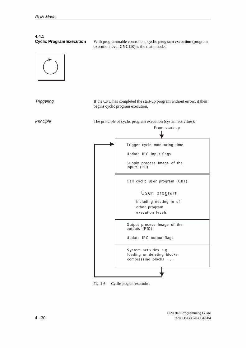
4.4.1Cyclic Program Execution With programmable controllers, cyclic program execution (program
execution level CYCLE ) is the main mode.
Triggering If the CPU has completed the start-up program without errors, it thenbegins cyclic program execution.
Principle The principle of cyclic program execution (system activities):
From start-up
Tr igger cycle monitor ing t ime
Update IPC input f lags
Supply process image of theinputs (PII)
Cal l cycl ic user program (OB1)
User program
other program
execut ion levels
including nest ing in of
Output process image of theoutputs (PIQ)
Update IPC output f lags
System act iv i t ies e.g.loading or delet ing blockscompressing blocks . . .
Fig. 4-6 Cyclic program execution
RUN Mode
CPU 948 Programming Guide
4 - 30 C79000-G8576-C848-04

User interface OB 1 During cyclic program execution, organization block OB 1 is calledregularly as the user interface. The STEP 5 user program in OB 1 isprocessed from the beginning with the block calls you haveprogrammed. After the system activities, the CPU starts again fromthe beginning with the first STEP 5 statement in OB 1.
In OB 1, you program the calls for program, function and sequenceblocks to be executed within the cyclic program.
Interrupt points Cyclic program execution can be interrupted by the following:
•• time-controlled program execution at block or operationboundaries,
•• process interrupt-driven program execution via input byte IB 0 atblock boundaries,
•• interrupt-driven program execution (interrupts INT A/B/C/D, E, F,G) at block or operation boundaries..
You specify the type of interrupt (at block or operation boundaries) indata block DX 0 (refer to Chapter 7).
Cyclic program execution can be interrupted or aborted regardless ofthe parameter setting in DX 0 as follows:
•• when a device fault or program error occurs (at operationboundaries,
•• by operator intervention:- stop switch, HALT (at operation boundaries),- PG function (at checkpoints - refer to Chapter 11),
•• by the stop command STS (at operation boundaries),
•• by a power failure on the central controller or in the expansion unit(at operation boundaries).
RUN Mode
CPU 948 Programming Guide
C79000-G8576-C848-04 4 - 31
4.4.2Specifying Time andInterrupt-Driven ProgramExecution
With time and interrupt-driven program execution, various types areavailable which can at present only be used as alternatives (i.e. notmixed). You decide which of the types of processing you want to useby setting the parameter in data block DX 0 (refer to Chapter 7).
"Process interrupts via IB 0" The execution mode "process interrupts via IB 0" has the followingfeatures:
•• only possible in single processor operation,
•• the nesting of higher priority program levels is only possible atblock boundaries,
•• the delayed interrupt (processed by OB 6) cannot be used,
•• the time-controlled interrupt (processing by OB 9) cannot be used.
"System interrupts" mode The "system interrupts" mode is characterized by the followingfeatures:
•• single or multiprocessor mode possible,
•• higher priority program levels are nested at block or commandboundaries,
•• delayed interrupts are processed by OB 6,
•• time-controlled interrupts are processed by OB 9.
Interrupting time andinterrupt-driven programexecution
Time and interrupt-driven program execution can be interrupted oraborted regardless of the parameter setting in DX 0 as follows:
•• when a device fault or program error occurs (at operationboundaries,
•• by operator intervention:- stop switch, HALT (at operation boundaries),- PG function (at checkpoints - refer to Chapter 11),
•• by the stop command STS (at operation boundaries),
•• by a power failure on the central controller or in the expansion unit(at operation boundaries).
RUN Mode
CPU 948 Programming Guide
4 - 32 C79000-G8576-C848-04
4.4.3Time-Controlled ProgramExecution
This type of program execution includes the delayed interrupt, thetime-controlled interrupt and cyclic timed interrupts.
All these interrupts are time-controlled.
Time-controlled program execution uses the TIMED INTERRUPTSlevel.
Delayed interrupts Triggered once after a selected delay time in the millisecond range.Organization block OB 6 is called with this interrupt.
Clock-controlled interrupt Triggered at a selected interval or once at an absolute point in time.Organization block OB 9 is called with this interrupt.
Cyclic timed interrupt Triggered at 9 different intervals. Each timed interrupt is assigned anorganization block (OB 10 to OB 18). This involves fixed cycles, i.e.the interval between two program stops is fixed.
Priorities Within time-controlled program execution, the following priorities areset:
Delayed interrupt OB 6cyclic timed int., period 1cyclic timed int., period 2cyclic timed int., period 3cyclic timed int., period 4cyclic timed int., period 5cyclic timed int., period 6cyclic timed int., period 7cyclic timed int., period 8cyclic timed int., period 9time-controlled interrupt
OB 6OB 10, shortest periodOB 11OB 12OB 13 ascendingOB 14 priorityOB 15OB 16OB 17OB 18, longest periodOB 9
NoteTime-controlled interrupt servicing in OB 6 and in OB 9 is onlypossible when the parameter "process interrupts via IB 0 = off" isset in DX 0. With the default setting in DX 0 ("process interruptsvia IB 0 = on") the corresponding process interrupts of IB 0 areprocessed using OB 6 and OB 9 (refer to Section 4.5.4).
RUN Mode
CPU 948 Programming Guide
C79000-G8576-C848-04 4 - 33
Delayed interrupt With the delayed interrupt of the CPU 948, small time intervals with aresolution of 1 ms can be set. Once the selected time has elapsed, thesystem program calls OB 6 once.
Resolution The delayed interrupt is generated by calling the special functionorganization block OB 153 (refer to Section 6.14). As soon as thedelay time assigned with OB 153 has elapsed, the system programinterrupts the current program execution and calls OB 6 (programexecution level TIMED INTERRUPTS). Following this, programexecution is resumed at the point at which it was interrupted.
The use of the delayed interrupt is, however, only possible when"process interrupts via IB 0 = off" is set in the data block DX 0.
User interface OB 6
OB 6 is called as the user interface for a delayed interrupt. In OB 6, youwrite a STEP 5 program to be executed in this situation. If OB 6 is notloaded, program execution is not interrupted.
Interruptions With the default setting, the TIMED INTERRUPTS level has thehighest priority of the basic levels (can be modified by changing theparameter assignment in DX 0).
In timed-controlled program execution, the servicing of the delayedinterrupt has highest priority.
Owing to the distribution of priorities, the processing of the delayedinterrupt cannot be interrupted by any other user program.
Special features •• A delayed interrupt is only processed in the RUN mode. Delayedinterrupts owing in the STOP mode, during power down orSTART-UP are discarded.
•• A generated delayed alarm (= OB 153 call was processed) is notretained in the transition to the STOP mode and during POWEROFF.
RUN Mode
CPU 948 Programming Guide
4 - 34 C79000-G8576-C848-04
•• If you generate a new delayed interrupt, i.e. call OB 153 withnew parameters, a previously set delayed interrupt is cancelled.A delayed interrupt currently being processed is continued. Thismeans that only one delayed interrupt is valid at any one time.
•• If a delayed interrupt occurs without the previous one beingcompletely processed, the new interrupt is discarded. Delayedinterrupts are not checked for collisions!
•• Note the special functions OB 122 and OB 142 with which youcan disable or delay the servicing of delayed interrupts.
Clock-controlled interrupt The CPU 948 has a battery-backed clock (central back-up via thepower supply of the central controller), which you can set and read outusing the STEP 5 program. This clock allows time-controlledexecution of a program section.
While the delayed interrupt is used for fast events, time-controlledinterrupts are particularly suitable for processing events which occuronce or which occur at longer intervals, e.g. hourly, daily or monthly.Once the point in time is reached, the system program calls OB 9.
Triggering A clock-controlled interrupt (timed job) is generated by calling thespecial function organization block OB 151 (refer to Section 6.13).Once the time set in OB 151 is reached (a time, a date) the timed job isexecuted. The system program interrupts the current programexecution and calls OB 9 (program execution level TIMEDINTERRUPTS). Following this, program execution is resumed at thepoint at which it was interrupted.
To use the clock-controlled interrupt, "process interrupts via IB 0 =off" must be set in data block DX 0.
User interface OB 9 For a clock-controlled interrupt, OB 9 is called as the user interface. InOB 9, you write a STEP 5 program to be processed when the OB iscalled. If OB 9 is not loaded, program execution is not interrupted.
RUN Mode
CPU 948 Programming Guide
C79000-G8576-C848-04 4 - 35

Interruptions Owing to the default, the TIMED INTERRUPTS layer has the highestpriority of the basic layers (can be modified in DX 0).
In time-controlled program execution, the execution ofclock-controlled interrupts has the lowest priority. This can thereforebe interrupted by the processing of a delayed interrupt or a cyclictimed interrupt.
Special features •• A clock-controlled interrupt is only processed in the RUN mode.Clock-controlled interrupts occurring in the STOP mode, whenthere is a power failure or during START-UP are discarded.
•• Once a clock-controlled interrupt has been generated (= OB 151call has been processed) it is retained in a WARM RESTART andfollowing POWER DOWN/POWER UP; it is, however, deletedduring a COLD RESTART.
•• If you generate a new clock-controlled interrupt, i.e. callOB 151 with new time values, a previously set clock-controlledinterrupt is cancelled. A clock-controlled interrupt currentlybeing processed is continued. This means that only oneclock-controlled interrupt is valid at any one time.
•• If a time-controlled interrupt occurs without the previous onebeing completely processed, the clock time-controlled interrupt isdiscarded. Clock-controlled interrupts are not checked forcollisions!
•• Note the special functions OB 122 and OB 142 with which youcan disable or delay the servicing of clock-controlled interrupts.
RUN Mode
CPU 948 Programming Guide
4 - 36 C79000-G8576-C848-04

Cyclic timed interrupts On the CPU 948, you can process 9 different time-controlledprograms, each being called at a different cyclic interval.
Triggering The basic clock pulse for timed interrupt processing is set to 100 ms.Using a special parameter in data block DX 0, you can adjust this insteps of 10 ms (basic clock pulse = yy * 10 ms where: 01H ≤ yy ≤FFH).
You can base the setting of the clock pulse on the shortest timerequired by your application for cyclic processing.
Time interval Cyclic timed interrupts are processed at fixed intervals with 9 possibleintervals (periods). Each interval is assigned to a specific organizationblock. You can select between two sets of intervals. You select thesets of intervals using a special parameter in data block DX 0.the following table illustrates the two sets of intervals with theassignment of the different intervals to organization blocks.
Interval set 1(default )
Interval set 2 OB called
1x basic clock pulse2 x basic clock pulse5 x basic clock pulse10 x basic clock pulse20 x basic clock pulse50 x basic clock pulse100 x basic clock pulse200 x basic clock pulse500 x basic clock pulse
1 x basic clock pulse2 x basic clock pulse4 x basic clock pulse8 x basic clock pulse16 x basic clock pulse32 x basic clock pulse64 x basic clock pulse128 x basic clock pulse256 x basic clock pulse
OB 10OB 11OB 12OB 13OB 14OB 15OB 16OB 17OB 18
NoteThe first TIMED INTERRUPT OB call following the start-uptakes place within the time assigned to the OB.
If, for example, the interrupt time "500 s" is set for OB 18 (basicclock pulse setting in DX 0 = 1 s and time base = 1), then the firstOB 18 call takes place after approximately 20 s following aCOLD RESTART. All further calls are then at intervals of 500 s.
Table 4-5 Sets of intervals and intervals of the TIMED INTERRUPTS
RUN Mode
CPU 948 Programming Guide
C79000-G8576-C848-04 4 - 37
User interfacesOB 10 to OB 18
When a timed interrupt occurs, the corresponding organization blockis called as the user interface at the next block boundary (or operationboundary).
For example, you would program the routine to be inserted in cyclicprogram execution every 100 ms in OB 10 (default).
The timed interrupt is only processed if the assigned organizationblock is loaded. If none of the organization blocks OB 10 to OB 18are loaded, there is no time-controlled program execution and thecyclic program is not interrupted.
You can disable the execution of timed interrupts by setting aparameter in data block DX 0, e.g. for testing your program.
Interruptions As default, the TIMED INTERRUPTS level has the highest priority ofthe basic levels (can be modified in DX 0).
Owing to the distribution of priority within time-controlled programexecution, the following interruptions in the processing of a cyclictimed interrupt are possible:
•• the processing of a cyclic timed interrupt can be interrupted by theprocessing of a delayed interrupt
•• organization blocks with shorter time bases have higher priorityand can interrupt organization blocks with longer time bases (e.g.OB 12 can interrupt OB 17).
NoteWith the three shortest time bases (OB 10 to 12) multipleprocessing without interruption is possible. If, for example, whileOB 10 is being processed, a further timed interrupt for OB 10occurs, the currently active processing of OB 10 is firstcompleted. Following this, OB 10 is called immediately again. If,however, there are more than three timed interrupts pending forone of the time bases, a collision of timed interrupts error occurs.
RUN Mode
CPU 948 Programming Guide
4 - 38 C79000-G8576-C848-04
Collision of timed interrupts In the CPU 948 there are two different types of collisions of timedinterrupts:
Type of error/cause ISTACK ID Reaction of the CPU
Timed interrupt queue overflow:- there are more than three
timed interrupts pending for one of the three shortest time bases (OB 10to 12),
- one of the other OBs (OB 13 to 18)is called again before it has beencompletely processed.
In the "ISTACK output" ofthe programmer, the error IDWEFES is marked in thecontrol bits.
The system program callsOB 33 as the user interface.If this is not loaded, the CPUchanges to the stop mode.
If the program can be interrupted atblock boundaries, the timed processingis blocked by the run time of a block inthe cyclic user program; the run time ofthe block is longer than the basic clockrate set in DX 0.
In the "ISTACK output" onthe programmer, the error IDWEFEH is marked in thecontrol bits.
The system program callsOB 33 as the user interface.If this is not loaded, thesystem program continuesprogram execution.
Error reactionOB 33
In OB 33, you can program the required reaction to the interruptcollisions listed above. When OB 33 is called, the system programenters a collision ID in ACCU-1-L (bit nos. 0 to 9). You can see themeaning of these bits (bit = ’1’) in the following table.
Bit number Meaning
0
1
2
Queue overflow in timed interrupt period 1 (more than three timed interrupts arepending for OB 10).Queue overflow in timed interrupt period 2 (more than three timed interrupts arepending for OB 11).Queue overflow in timed interrupt period 3 (more than three timed interrupts arepending for OB 12).
3
4
Queue overflow in timed interrupt period 4 (OB 13 has been called again before theprior call was completely executed).Queue overflow in timed interrupt period 5 (OB 14 has been called again before theprior call was completely executed).
Table 4-6 Timed interrupt collision IDs: meaning of the bits in ACCU-1-L
RUN Mode
CPU 948 Programming Guide
C79000-G8576-C848-04 4 - 39
Bit number Meaning
5
6
7
8
Queue overflow in timed interrupt period 6 (OB 15 has been called again before theprior call was completely executed).Queue overflow in timed interrupt period 7 (OB 16 has been called again before theprior call was completely executed).Queue overflow in timed interrupt period 8 (OB 17 has been called again before theprior call was completely executed).Queue overflow in timed interrupt period 9 (OB 18 has been called again before theprior call was completely executed).
9 Timed interrupt clock pulse masked for too long.
After processing OB 33, the program is resumed at the interruptedtimed interrupt OB.
NoteIf "interruptability at block boundaries" is set, following a collisionof timed interrupts, the SAC does not point to the block at whoseboundary the collision of timed interrupts took place (BEstatement) but rather to the block which called the block thatcaused the error (the return address). You can set the followingparameters in data block DX 0 (refer to Chapter 7) fortime-controlled program execution:- setting the basic clock rate- setting the clock distributor,- setting priorities relative to interrupt-driven program execution,- enabling/disabling timed interrupt processing.
RUN Mode
CPU 948 Programming Guide
4 - 40 C79000-G8576-C848-04
4.4.4Interrupt-Driven ProgramExecution
Depending on the selected mode, two different types of interrupt-drivenprogram execution are possible with the CPU 948:
•• PROCESS INTERRUPTS via input byte IB 0 (max. 8 interrupts),
•• INTERRUPTSvia signal lines of the S5 bus (max. 4 interrupts).
PROCESS INTERRUPTS viainput byte IB 0
To service process interrupts, the default "process interrupts via IB 0 =on" must not be changed in the data block DX 0.
Program execution controlled by process interrupts means that asignal change in the input byte IB 0 causes the current programexecution to be interrupted and a special program section to beexecuted.
NoteIf you enable "servicing process interrupts via IB 0" you cannotuse the delayed interrupt, the time-controlled interrupt and thesystem interrupt.
Triggering The signal state change of a bit in input byte IB 0 triggers the processinterrupt.
User interfaces OB 2 to OB 9
If a process interrupt occurs, one of the OBs listed in the followingtable is called as the user interface.
Signal state change in IB 0 with bit OB called
I 0.0I 0.1I 0.2I 0.3I 0.4I 0.5I 0.6I 0.7
OB 2OB 3OB 4OB 5OB 6OB 7OB 8OB 9
Table 4-7 User interfaces for process interrupts
RUN Mode
CPU 948 Programming Guide
C79000-G8576-C848-04 4 - 41

In the organization blocks OB 2 to OB 9, you program the part of yourSTEP 5 program to be executed when one of the process interruptsoccurs indicated by a bit in input byte IB 0.If the corresponding OB is not loaded, program execution is notinterrupted. No interrupt-driven program processing takes place.
NoteIf the I/O module no longer acknowledges when the CPU accessesIB 0, the system program recognizes a timeout and calls the userinterface OB 28. If OB 28 is not loaded, the CPU changes to thestop mode.
Priority of process interrupts The default setting means that PROCESS INTERRUPTS have a lowerpriority than the TIMED INTERRUPTS level.A parameter in data block DX 0 allows you to change the default sothat the PROCESS INTERRUPTS level has a higher priority than theTIMED INTERRUPTS level.
The following priorities are set for process interrupt processing:
I 0.0I 0.1I 0.2I 0.3I 0.4I 0.5I 0.6I 0.7
OB 2OB 3OB 4 ascendingOB 5 priorityOB 6OB 7OB 8OB 9
With process interrupts, no nested execution is possible. When aprocess interrupt OB has been completely processed and there arefurther process interrupts pending, the system program calls the OBwith the next lower priority and processes it.The PROCESS INTERRUPTS level is only exited when each signalchange in input byte IB 0 has been dealt with and the correspondingOB completely processed.
NoteProcess interrupt-driven program execution cannot be interruptedby further process interrupt-driven program execution.
RUN Mode
CPU 948 Programming Guide
4 - 42 C79000-G8576-C848-04
INTERRUPTS via signallines of the S5 bus
Interrupt-driven program execution means that an S5 bus signal froman I/O module with interrupt capability (e.g. digital inputs, IPs, CPs)causes the CPU to interrupt program execution and to process aspecific section of program.
NoteIf you want to use interrupt-driven program execution via S5 bussignal lines on your CPU, you must set "process interrupts via IB 0= off" in DX 0 and activate the individual interrupts by means ofDX 0 parameters. The interrupts must also be enabled withjumpers on the module (refer to the Appendix and /2/). In contrastto the CPU 946/947, you can set "interrupt at block boundaries" or"interrupt at operation boundaries" as the mode in DX 0.
Jumper settings for systeminterrupts
For interrupt-driven program execution with the CPU 948, there arefour system interrupts available to you:
- INT A/B/C/D (dependent on the slot in the CPU, see the SystemManual (Further Reading /2/)),
- INT E- INT F
and- INT G.
The interrupts you want to use must be enabled with the suppliedjumpers. The jumper plug is located on the basic board above thereceptacle for the memory card. The exact position can be seen inAppendix 1.
RUN Mode
CPU 948 Programming Guide
C79000-G8576-C848-04 4 - 43

Triggering The active state of an interrupt line on the S5 bus triggers theinterrupt. The interrupt signal is level-triggered (low level). Toacknowledge the interrupt, please refer to the operating instructionsfor the module which triggers the interrupt.
User interfaces OB 2 to OB 5
If an interrupt occurs, one of the OBs listed in the following table iscalled as the user interface.
Interrupt triggered by OB called
Interrupt signal X (A, B, C or D, slot-dependent) Interrupt signal EInterrupt signal FInterrupt signal G
OB 2
OB 3OB 4OB 5
If, for example, the interrupt signal ’F’ occurs, the system programcalls OB 4.
If the relevant OB is not loaded, program execution is not interrupted.There is no interrupt-driven program execution.
Priority of process interrupts The default setting means that PROCESS INTERRUPTS have a lowerpriority than the TIMED INTERRUPTS level.A parameter in data block DX 0 allows you to change the default sothat the process interrupts level has a higher priority than the TIMEDINTERRUPTS level.
Within interrupt servicing, the priorities of the individual interruptsare specified as follows:
•• If there are several interrupts pending, the correspondingorganization blocks are called according to the order of priorityyou specify in DX 0 (single priority).
You can specify priority levels 1 to 5 for the four interrupts.
Table 4-8 User interfaces for interrupts
RUN Mode
CPU 948 Programming Guide
4 - 44 C79000-G8576-C848-04

When an interrupt OB has been completely executed and there arefurther interrupts pending, the system program calls and processes theOB with the next lowest priority.The INTERRUPTS processing level is only exited when every activesignal state (low level) of an interrupt line on the S5 bus has beendealt with and the corresponding OB has been completely processed.
NoteInterrupt-driven program execution cannot be interrupted by thesame interrupt occurring again.
Disabling interrupt-drivenprocessing
An interrupt-driven program is called at a block or STEP 5 operationboundary in the cyclic program. This interrupt can cause problems whena cyclic section of program must be processed within a certain time (e.g.to achieve a certain reaction time) or when a series of operations must notbe interrupted (e.g. when reading or writing interdependent values).
If a program section must not be interrupted by interrupt-drivenprocessing, the following strategies are possible:
Interrupts at block boundaries •• Program this program section so that it does not contain a blockchange. Program sections that do not contain a block change canthen not be interrupted.
•• Use OB 122 with which you can disable the processing of processinterrupts for a specific program section. Remember, however, thatthe timed interrupts are also disabled (refer to Section 6.3).
•• Program the STEP 5 operation ’IA’ (disable process interrupts).With the operation ’RA’ (enable process interrupts) you can enableinterrupt processing again.
Between these two operations, no process interrupt-drivenprogram execution is permitted. The program section betweenthese two operations cannot be interrupted.
•• ’IA’ and ’RA’ are only possible in function blocks (extendedoperation set - refer to Section 3.5.4) and only apply to processinterrupts via IB 0.
NoteIf a process interrupt is disabled using OB 22 or delayed usingOB 142, the RA operation is not effective.
RUN Mode
CPU 948 Programming Guide
C79000-G8576-C848-04 4 - 45

Interrupts at operationboundaries
•• Program the section that must not be interrupted in an interrupt OBand assign the highest priority to it.
•• Use the special function OB 122. With this, you can disableinterrupts and timed interrupts (refer to Section 6.3).
•• Using the operation LIM and SIM (system operations - refer toSection 3.5.4) read or set the 32-bit interrupt mask.
Interrupt servicing can be disabled completely or separately forindividual interrupts in data block DX 0. This is, however, onlypossible following a COLD RESTART (refer to Chapter 7), sinceDX 0 is only evaluated in a COLD RESTART.
Reaction time The time required to react to a process interrupt/interrupt requestcorresponds to the processing time of a block (for interrupts at blockboundaries) or a STEP 5 operation (for interrupts at operationboundaries). If, however, at the time the cyclic program is interruptedthere are higher priority timed interrupts pending, the interrupt-drivenprogram is only executed when all the pending timed interrupts havebeen completely processed.
The maximum reaction time between the occurrence and execution ofa process interrupt/hardware interrupt is increased in this case by theprocessing time of the higher priority timed interrupts.
Program execution levelsand flags
If you run your user program not only cyclically but also time andinterrupt-driven, you run the risk of overwriting flags.This is the case when the same flag areas are accessed at differentprogram processing levels.
It is therefore advisable to assign flags to individual programprocessing levels or at the beginning of time or interrupt-drivenprogram execution, to "save" the signal states of multiply assignedflags in a data block and to write the values back at the end of theinterrupt servicing. The same applies for a warm restart.
To avoid double use of flags, you can also use the S flags for mostapplications. Special "saving" strategies for flags are then no longernecessary, providing the S flags are assigned exclusively to individualprogram processing levels (there are enough S flags available).
RUN Mode
CPU 948 Programming Guide
4 - 46 C79000-G8576-C848-04
Contents of Chapter 5
5.1 Frequent Errors in the User Program. . . . . . . . . . . . . . . . . . . . . . . . . . . . . . . . . . . . . . . . . 5 - 4
5.2 Error Information . . . . . . . . . . . . . . . . . . . . . . . . . . . . . . . . . . . . . . . . . . . . . . . . . . . . . . . . 5 - 5
5.3 Procedure for Error Analysis . . . . . . . . . . . . . . . . . . . . . . . . . . . . . . . . . . . . . . . . . . . . . . . 5 - 8
5.4 Control Bits and Interrupt Stack . . . . . . . . . . . . . . . . . . . . . . . . . . . . . . . . . . . . . . . . . . . . 5 - 9
5.4.1 Control Bits. . . . . . . . . . . . . . . . . . . . . . . . . . . . . . . . . . . . . . . . . . . . . . . . . . . . . . . . . . . . 5 - 105.4.2 ISTACK Content. . . . . . . . . . . . . . . . . . . . . . . . . . . . . . . . . . . . . . . . . . . . . . . . . . . . . . . . 5 - 145.4.3 Example of Error Diagnosis using the ISTACK . . . . . . . . . . . . . . . . . . . . . . . . . . . . . . . 5 - 19
5.5 Error Handling Using Organization Blocks. . . . . . . . . . . . . . . . . . . . . . . . . . . . . . . . . . . 5 - 20
5.6 Causes of Error and Reactions of the CPU . . . . . . . . . . . . . . . . . . . . . . . . . . . . . . . . . . . 5 - 23
5.6.1 OB 19: Calling a Logic Block That Is Not Loaded (KB). . . . . . . . . . . . . . . . . . . . . . . . 5 - 245.6.2 OB 19: Calling a Data Block That Is Not Loaded (KDB) . . . . . . . . . . . . . . . . . . . . . . . 5 - 245.6.3 OB 23/24, OB 28/29: Timeout Error (QVZ). . . . . . . . . . . . . . . . . . . . . . . . . . . . . . . . . . 5 - 255.6.4 OB 25: Addressing Error (ADF) . . . . . . . . . . . . . . . . . . . . . . . . . . . . . . . . . . . . . . . . . . . 5 - 265.6.5 OB 26: Cycle Time Exceeded Error (ZYK) . . . . . . . . . . . . . . . . . . . . . . . . . . . . . . . . . . 5 - 275.6.6 OB 27: (Substitution Error SUF) . . . . . . . . . . . . . . . . . . . . . . . . . . . . . . . . . . . . . . . . . . . 5 - 285.6.7 OB 30: Parity Error and Timeout Error in the User Memory (PARE). . . . . . . . . . . . . . 5 - 285.6.8 OB 32: Load and Transfer Error (TRAF) . . . . . . . . . . . . . . . . . . . . . . . . . . . . . . . . . . . . 5 - 295.6.9 OB 33: Collision of Timed Interrupts Error (WEFES/WEFEH) . . . . . . . . . . . . . . . . . . 5 - 305.6.10 OB 34: Error with G DB/GX DX (FEDBX). . . . . . . . . . . . . . . . . . . . . . . . . . . . . . . . . . 5 - 325.6.11 OB 35: Communication Errors . . . . . . . . . . . . . . . . . . . . . . . . . . . . . . . . . . . . . . . . . . . . 5 - 325.6.12 OB 36: Error in Self-test . . . . . . . . . . . . . . . . . . . . . . . . . . . . . . . . . . . . . . . . . . . . . . . . . 5 - 33
5.7 Self-Test . . . . . . . . . . . . . . . . . . . . . . . . . . . . . . . . . . . . . . . . . . . . . . . . . . . . . . . . . . . . . . 5 - 34
5.7.1 Overview. . . . . . . . . . . . . . . . . . . . . . . . . . . . . . . . . . . . . . . . . . . . . . . . . . . . . . . . . . . . . . 5 - 345.7.2 Description of the Test Functions. . . . . . . . . . . . . . . . . . . . . . . . . . . . . . . . . . . . . . . . . . . 5 - 355.7.3 Settings . . . . . . . . . . . . . . . . . . . . . . . . . . . . . . . . . . . . . . . . . . . . . . . . . . . . . . . . . . . . . . . 5 - 375.7.4 Error Handling . . . . . . . . . . . . . . . . . . . . . . . . . . . . . . . . . . . . . . . . . . . . . . . . . . . . . . . . . 5 - 38
5Interrupt and Error Diagnostics
CPU 948 Programming Guide
C79000-G8576-C848-04 5 - 1

Contents
CPU 948 Programming Guide
5 - 2 C79000-G8576-C848-04
5Interrupt and Error Diagnostics
This chapter explains how to avoid errors when planning andprogramming your STEP 5 programs. You will see what help you can get from the system program fordiagnosing and reacting to errors and which blocks you can use toprogram reactions to errors.At the end of the chapter, you will learn how to activate integratedsystem functions for a self-test of the CPU 948.
CPU 948 Programming Guide
C79000-G8576-C848-04 5 - 3
5.1 Frequent Errors in the User Program
The system program can detect effects of errors in the user program,faulty operation of the CPU, or errors in the system programprocessing.
The following list describes errors that occur most frequently duringthe start-up of the user program. You can avoid these errors by doingthe following when you write you STEP 5 program.
•• When specifying byte addresses for I/Os, make sure that thecorresponding modules are plugged into the central controller orthe expansion unit.
•• Make sure that you have provided correct parameters for alloperands.
•• Be careful when changing function blocks. Check to see that theFBs/FXs are assigned the correct operands and that the actualoperands are specified.
•• Make sure that outputs, flags, timers, and counters are notprocessed in several locations in the program with operations thatcounteract each other.
•• Make sure that timers are scanned only once per cycle (e.g., A T1).
•• Make sure that all data blocks called in the program exist and are longenough.
•• Check to see if all blocks called are actually in the memory.
•• If required by other blocks (e.g. standard function blocks),scratchpad flags should be saved by interrupt-driven andtime-controlled programs and loaded again when these programsections have been completed.
Frequent Errors in the User Program
CPU 948 Programming Guide
5 - 4 C79000-G8576-C848-04

5.2 Error Information
If an error occurs during system start-up or during cyclic processing ofyour program, the sources of information described in this section canhelp you to find the problem. This includes:
•• LEDs on the front panel of the CPU
•• interrupt stack ISTACK and control bits
•• block stack BSTACK
The following sections explain the ways of evaluating this informationand how to use the information to analyze problems.
LEDs on the front panel of the CPU
If the CPU goes into the STOP mode when you do not want it to,check the LEDs on the front panel. They can indicate the cause of theproblem.
LED display Meaning
STOP LED lit continuously The various states of the STOP LED indicate specific causes of interruptions and errors (see section 4.1).
STOP LED flashes slowly
STOP LED flashes quickly
SYS FAULT LED litcontinuously
ADF LED lit continuously Addressing error
QVZ LED lit continuously Timeout error
ZYK LED lit continuously Cycle time exceeded error
Error Information
CPU 948 Programming Guide
C79000-G8576-C848-04 5 - 5
PG online function OUTPUTISTACK
You can get information about the status of the control bits and thecontents of the interrupt stack (ISTACK) by using die PG onlinefunction OUTPUT ISTACK.
When the CPU goes into the STOP mode, the system program enters allthe information it requires for a warm restart in the ISTACK . Thisinformation includes:
•• contents of registers,
•• contents of accumulators,
•• STEP address counter SAC
and
•• results codes
Depending on where the interruption leading to the STOP occurred,the displayed information refers to user blocks or blocks of the systemprogram (OB 0).
These entries are a valuable aid in error diagnosis.
Before the actual ISTACK is output on the programmer, the status ofthe control bits is displayed. The control bits mark the currentoperating status and specific characteristics of the CPU and the userprogram and provide additional information on the cause of an error.
You can call the ISTACK programmer function not only when theCPU is in the STOP mode, but also when it is in the RESTART orRUN mode. However, in the RESTART and RUN modes, you canonly display the control bits (i.e., the first page of ISTACKinformation).
The meaning of the control bits and structure of the interrupt stack aredescribed in detail in Section 5.4.
Online function OUTPUTBSTACK
You can display the contents of the block stack (BSTACK - seesection 3.2 "Nesting blocks") using the PG online function OUTPUTBSTACK.
The BSTACK contains a listing of all blocks (blocks of the userprogram and organization block OB 0 of the system program) calledin sequence and not completely processed when the CPU went intothe STOP mode. Since the BSTACK is filled from the bottom, the topline of the BSTACK display contains the block that called the blockcontaining an error.
Error Information
CPU 948 Programming Guide
5 - 6 C79000-G8576-C848-04

In the first line, the information shown below is available:
Information Meaning
BLOCK NO Type and number of the block that called thefaulty block
BLOCK ADDR Absolute start address of the calling block inthe program memory
RETURN ADDR Absolute address of the first STEP 5 operationof this block in the user memory.
REL ADDR Relative address (= difference "RETURNADDR - BLOCK ADDR") of the nextoperation to be processed in the calling block.(You can display relative addresses on aprogrammer in the mode "disable input"/keyswitch and with S5-DOS from Stage IVupwards using the function key "addresses").
DB NO Number of the last data block opened in thecalling block
DB ADDR Absolute start address in the program memoryof the last data block opened in the callingblock (address of data word DW 0)
Example
Evaluating the BSTACK function:
BLOCK NO BLOCK ADDR RETURN ADDR REL ADDR DB NO DB ADDR
PB 3PB 2PB 1OB 1OB 66 1)
OB 63OB 62OB 61
00090000500004000010E2B10E0FC0E0490E0010
98514111E2C40E12FAE0CBEE0273
00008000010000100001001300033A0082E00263
00000000
1) The blocks executed before OB 1 are internal blocks belonging to the system program (the BSTACK is structured chronologically).
In the example, PB 3 called the faulty block at relative address "00008 - 1 = 00007".During the jump to this faulty block, no data block was open.
Error Information
CPU 948 Programming Guide
C79000-G8576-C848-04 5 - 7
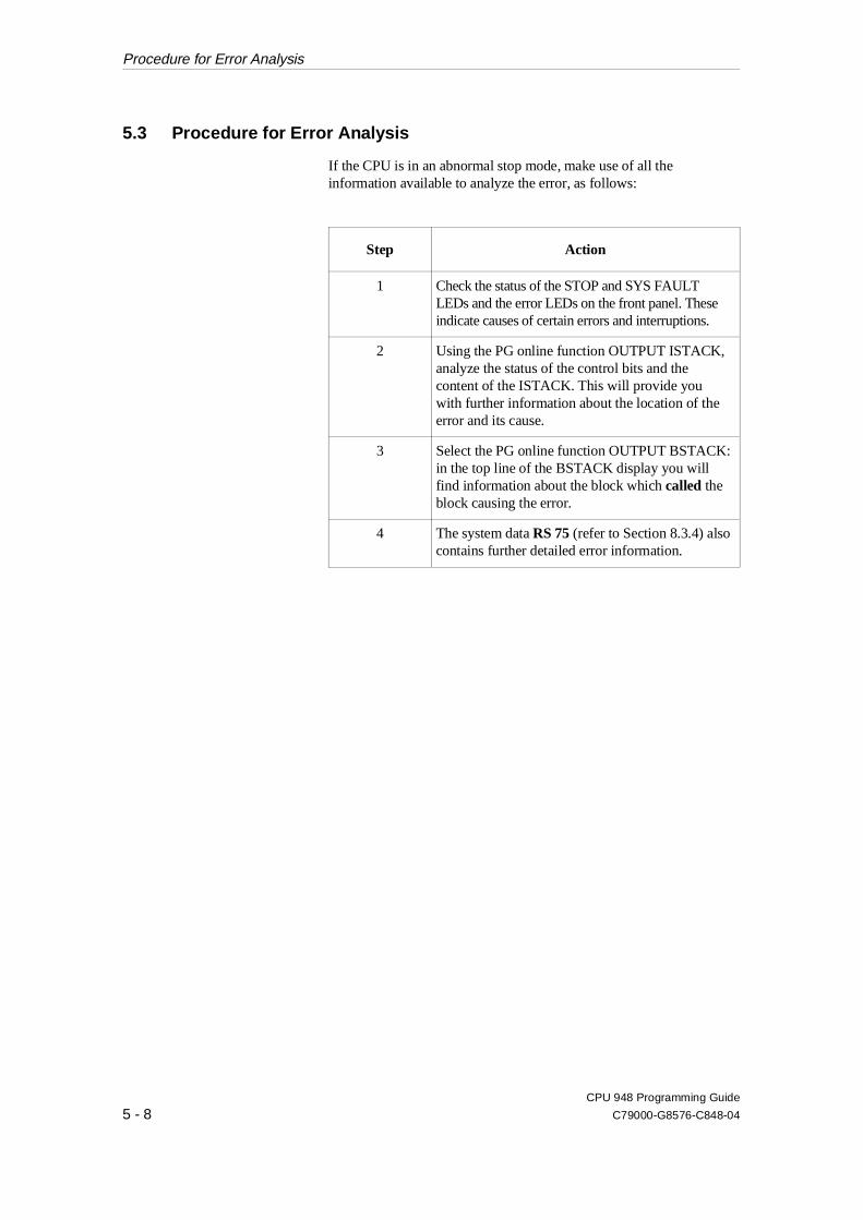
5.3 Procedure for Error Analysis
If the CPU is in an abnormal stop mode, make use of all theinformation available to analyze the error, as follows:
Step Action
1 Check the status of the STOP and SYS FAULTLEDs and the error LEDs on the front panel. Theseindicate causes of certain errors and interruptions.
2 Using the PG online function OUTPUT ISTACK,analyze the status of the control bits and thecontent of the ISTACK. This will provide youwith further information about the location of theerror and its cause.
3 Select the PG online function OUTPUT BSTACK:in the top line of the BSTACK display you willfind information about the block which called theblock causing the error.
4 The system data RS 75 (refer to Section 8.3.4) alsocontains further detailed error information.
Procedure for Error Analysis
CPU 948 Programming Guide
5 - 8 C79000-G8576-C848-04
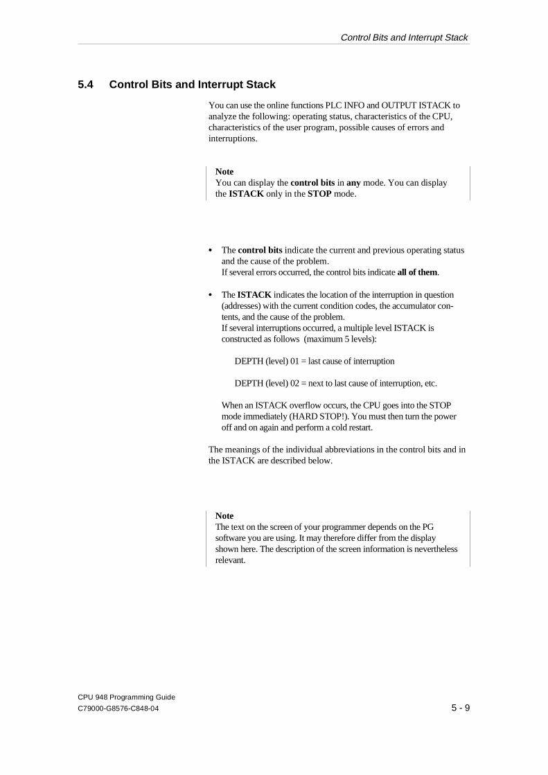
5.4 Control Bits and Interrupt Stack
You can use the online functions PLC INFO and OUTPUT ISTACK toanalyze the following: operating status, characteristics of the CPU,characteristics of the user program, possible causes of errors andinterruptions.
NoteYou can display the control bits in any mode. You can displaythe ISTACK only in the STOP mode.
•• The control bits indicate the current and previous operating statusand the cause of the problem.If several errors occurred, the control bits indicate all of them.
•• The ISTACK indicates the location of the interruption in question(addresses) with the current condition codes, the accumulator con-tents, and the cause of the problem.If several interruptions occurred, a multiple level ISTACK isconstructed as follows (maximum 5 levels):
DEPTH (level) 01 = last cause of interruption
DEPTH (level) 02 = next to last cause of interruption, etc.
When an ISTACK overflow occurs, the CPU goes into the STOPmode immediately (HARD STOP!). You must then turn the poweroff and on again and perform a cold restart.
The meanings of the individual abbreviations in the control bits and inthe ISTACK are described below.
NoteThe text on the screen of your programmer depends on the PGsoftware you are using. It may therefore differ from the displayshown here. The description of the screen information is neverthelessrelevant.
Control Bits and Interrupt Stack
CPU 948 Programming Guide
C79000-G8576-C848-04 5 - 9
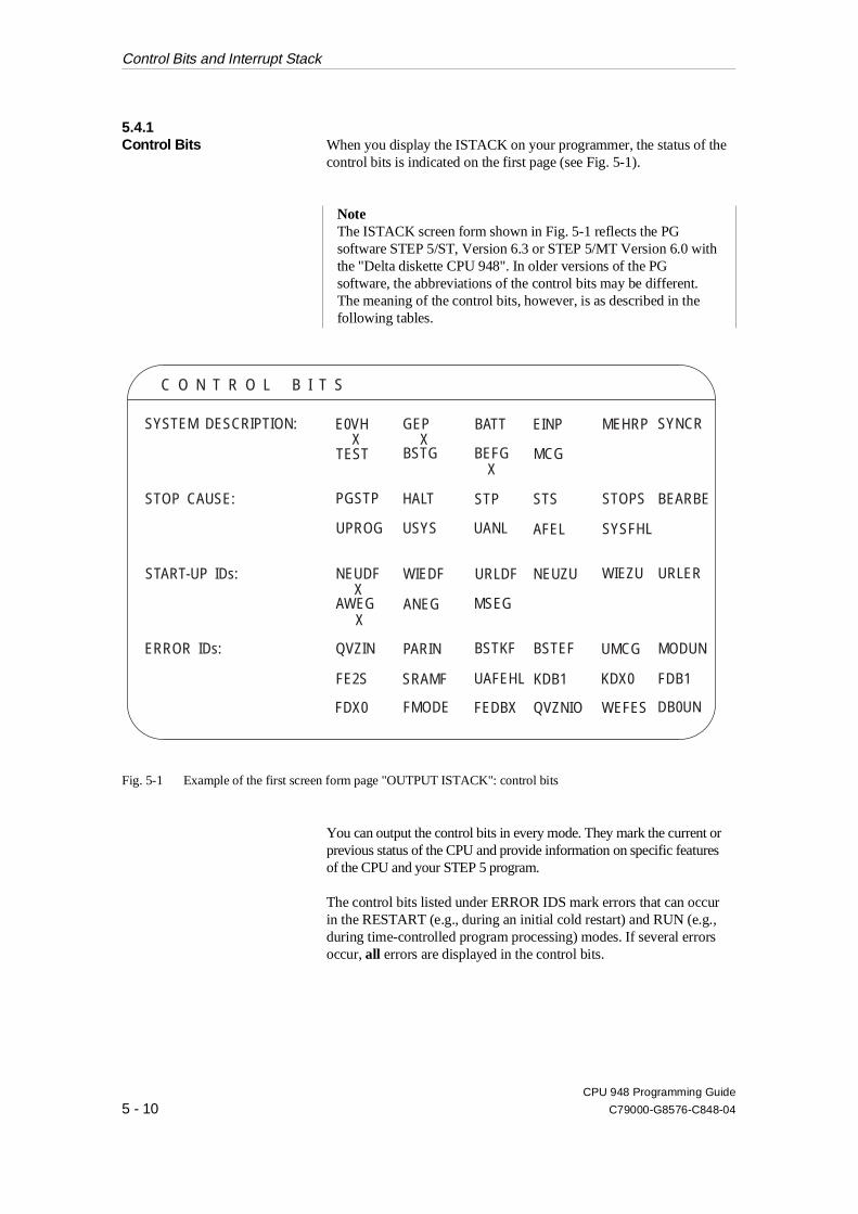
5.4.1Control Bits When you display the ISTACK on your programmer, the status of the
control bits is indicated on the first page (see Fig. 5-1).
NoteThe ISTACK screen form shown in Fig. 5-1 reflects the PGsoftware STEP 5/ST, Version 6.3 or STEP 5/MT Version 6.0 withthe "Delta diskette CPU 948". In older versions of the PGsoftware, the abbreviations of the control bits may be different.The meaning of the control bits, however, is as described in thefollowing tables.
You can output the control bits in every mode. They mark the current orprevious status of the CPU and provide information on specific featuresof the CPU and your STEP 5 program.
The control bits listed under ERROR IDS mark errors that can occurin the RESTART (e.g., during an initial cold restart) and RUN (e.g.,during time-controlled program processing) modes. If several errorsoccur, all errors are displayed in the control bits.
C O N T R O L B I T S
SYSTEM DESCRIPTION: E0VH GEP BATT EINP MEHRP SYNCR
TEST
STOP CAUSE:
START-UP IDs:
ERROR IDs:
PGSTP
UPROG
X
NEUDFX
XAWEG
QVZIN
FE2S
FDX0
XBSTG BEFG MCG
X
HALT STP STS STOPS BEARBE
USYS UANL AFEL SYSFHL
WIEDF URLDF NEUZU WIEZU URLER
ANEG MSEG
PARIN BSTKF BSTEF UMCG MODUN
SRAMF UAFEHL KDB1 KDX0 FDB1
FMODE FEDBX QVZNIO WEFES DB0UN
Fig. 5-1 Example of the first screen form page "OUTPUT ISTACK": control bits
Control Bits and Interrupt Stack
CPU 948 Programming Guide
5 - 10 C79000-G8576-C848-04

The following tables explain the meaning of the individual bits.
SYSTEM DESCRIPTION
Bit Meaning
E0VH Input byte IB 0 (process interrupts) exists, i.e. the digitalinput module addressed with ’0’ was plugged in duringthe last cold restart and the module acknowledged.
GEP Programmable controller has a central back-up battery.
BATT Battery failure in the central controller (BAU)
EINP Single processor operation
MEHRP Multiprocessing operation
SYNCR Start-up of the CPUs in multiprocessing operation issynchronized
TEST Test operation
BSTG DX-0 setting "interrupts at block boundaries"
BEFG DX-0 setting "interrupts at operation boundaries
MCG Memory card inserted
STOP CAUSE (see RS 7)
Bit Meaning
PGSTP STOP mode set from programmer
HALT Multiprocessor STOP mode:a) Selector switch on the coordinator (COR) is
in the STOP positionor
b) Stop status caused by command STOP operation from system program when the corresponding error OB is not loaded and an error occurs
STS STOP mode caused by STEP 5 operation ’STS’ (afterexecuting an operation)
STOPS STOP mode caused by setting the mode selector to theSTOP position
BEARBE STOP mode after the PROGRAM TEST ENDprogrammer function
Table 5-1 Meaning of the control bits SYSTEM DESCRIPTION
Table 5-2 Meaning of the control bits STOP CAUSE
Control Bits and Interrupt Stack
CPU 948 Programming Guide
C79000-G8576-C848-04 5 - 11
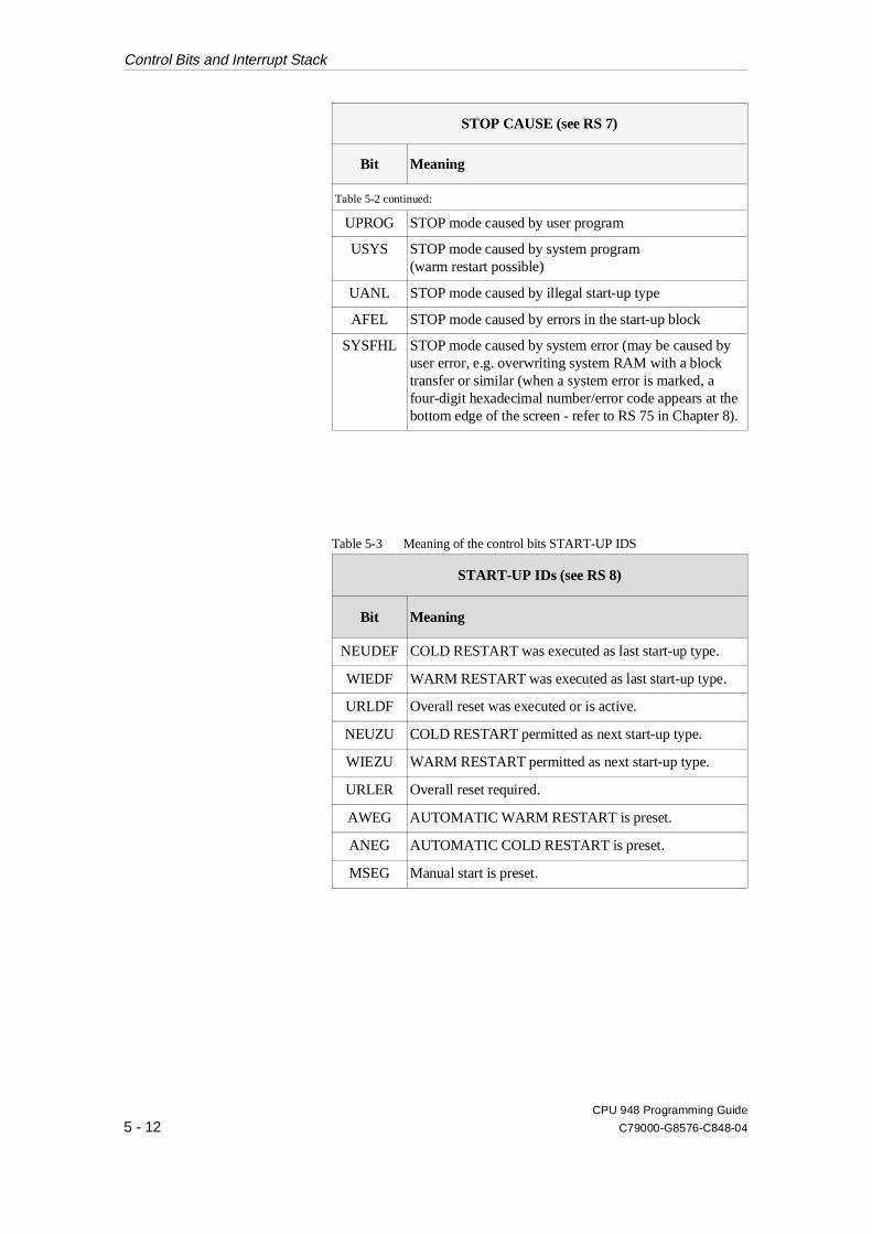
STOP CAUSE (see RS 7)
Bit Meaning
Table 5-2 continued:
UPROG STOP mode caused by user program
USYS STOP mode caused by system program(warm restart possible)
UANL STOP mode caused by illegal start-up type
AFEL STOP mode caused by errors in the start-up block
SYSFHL STOP mode caused by system error (may be caused byuser error, e.g. overwriting system RAM with a blocktransfer or similar (when a system error is marked, afour-digit hexadecimal number/error code appears at thebottom edge of the screen - refer to RS 75 in Chapter 8).
START-UP IDs (see RS 8)
Bit Meaning
NEUDEF COLD RESTART was executed as last start-up type.
WIEDF WARM RESTART was executed as last start-up type.
URLDF Overall reset was executed or is active.
NEUZU COLD RESTART permitted as next start-up type.
WIEZU WARM RESTART permitted as next start-up type.
URLER Overall reset required.
AWEG AUTOMATIC WARM RESTART is preset.
ANEG AUTOMATIC COLD RESTART is preset.
MSEG Manual start is preset.
Table 5-3 Meaning of the control bits START-UP IDS
Control Bits and Interrupt Stack
CPU 948 Programming Guide
5 - 12 C79000-G8576-C848-04
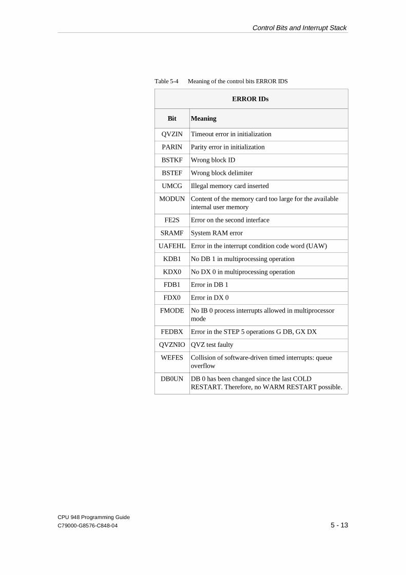
ERROR IDs
Bit Meaning
QVZIN Timeout error in initialization
PARIN Parity error in initialization
BSTKF Wrong block ID
BSTEF Wrong block delimiter
UMCG Illegal memory card inserted
MODUN Content of the memory card too large for the availableinternal user memory
FE2S Error on the second interface
SRAMF System RAM error
UAFEHL Error in the interrupt condition code word (UAW)
KDB1 No DB 1 in multiprocessing operation
KDX0 No DX 0 in multiprocessing operation
FDB1 Error in DB 1
FDX0 Error in DX 0
FMODE No IB 0 process interrupts allowed in multiprocessormode
FEDBX Error in the STEP 5 operations G DB, GX DX
QVZNIO QVZ test faulty
WEFES Collision of software-driven timed interrupts: queueoverflow
DB0UN DB 0 has been changed since the last COLDRESTART. Therefore, no WARM RESTART possible.
Table 5-4 Meaning of the control bits ERROR IDS
Control Bits and Interrupt Stack
CPU 948 Programming Guide
C79000-G8576-C848-04 5 - 13
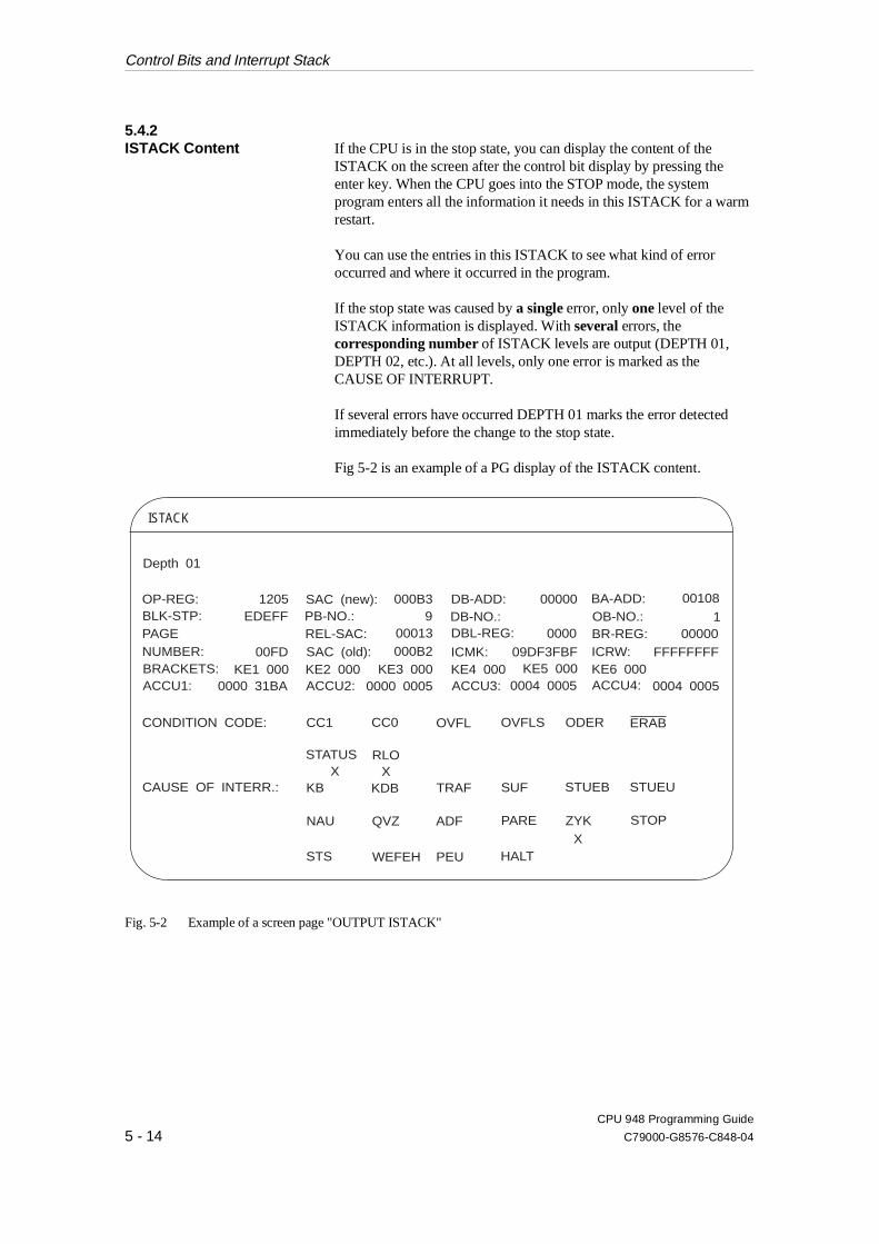
5.4.2ISTACK Content If the CPU is in the stop state, you can display the content of the
ISTACK on the screen after the control bit display by pressing theenter key. When the CPU goes into the STOP mode, the systemprogram enters all the information it needs in this ISTACK for a warmrestart.
You can use the entries in this ISTACK to see what kind of erroroccurred and where it occurred in the program.
If the stop state was caused by a single error, only one level of theISTACK information is displayed. With several errors, thecorresponding number of ISTACK levels are output (DEPTH 01,DEPTH 02, etc.). At all levels, only one error is marked as theCAUSE OF INTERRUPT.
If several errors have occurred DEPTH 01 marks the error detectedimmediately before the change to the stop state.
Fig 5-2 is an example of a PG display of the ISTACK content.
ISTACK
Depth 01
OP-REG:BLK-STP:PAGENUMBER:BRACKETS:ACCU1: 0000 31BA
1205EDEFF
00FDKE1 000
ACCU2:
SAC (new):PB-NO.:REL-SAC:SAC (old):KE2 000 KE3 000
0000 0005
000B39
00013000B2
ACCU3:
DB-ADD:DB-NO.:DBL-REG:
ICMK:KE4 000 KE5 000 KE6 000
0004 0005
00000
09DF3FBF
0000
ACCU4:
BA-ADD:OB-NO.:BR-REG:ICRW:
0004 0005
00108
00000FFFFFFFF
1
CONDITION CODE:
CAUSE OF INTERR.: KB
NAU
STS
KDB
QVZ
WEFEH
TRAF
OVFL
ADF
PEU
SUF
PARE
HALT
OVFLS
STUEB
ZYK
ODER
STUEU
STOP
ERAB
RLO
CC0
STATUSX X
X
CC1
Fig. 5-2 Example of a screen page "OUTPUT ISTACK"
Control Bits and Interrupt Stack
CPU 948 Programming Guide
5 - 14 C79000-G8576-C848-04

Explanation of the ISTACKscreen
DEPTH Information level of the ISTACK when more than one error hasoccurred:
DEPTH 01 = last cause of stop to occurDEPTH 02 = next to last cause of stop to occur......DEPTH05 = ...... (maximum depth)
Information about the error The following table contains information about the ISTACK IDs withwhich the statement in the user program can be found which causedthe CPU to change to the STOP mode.
Information about the error
ISTACK ID Meaning
OP-REG Operation register:Contains machine code (first word of theinstruction processed last in an interruptedprogram processing level.
SAC (new) STEP address counter (new):Contains the absolute address of the nextoperation in the program memory to beprocessed. When a warm restart occurs,the CPU continues the program with thisoperation.
DB-ADD Absolute start address (DW 0) in theprogram memory of the data block currentlyopened (= 0000 if no data block wasopened)
BA-ADD Absolute address in the program memoryfor the operation to be processed next in theblock where the last block call was made
BLK-STP Block stack (BSTACK) pointer:Contains the 20-bit offset address of the last BSTACK entry (always Exxxx).
PB-NO(depending on type
PB, OB ...)
Block type and number of the mostrecently processed block
Table 5-5 Meaning of the ISTACK IDs for errors
Control Bits and Interrupt Stack
CPU 948 Programming Guide
C79000-G8576-C848-04 5 - 15
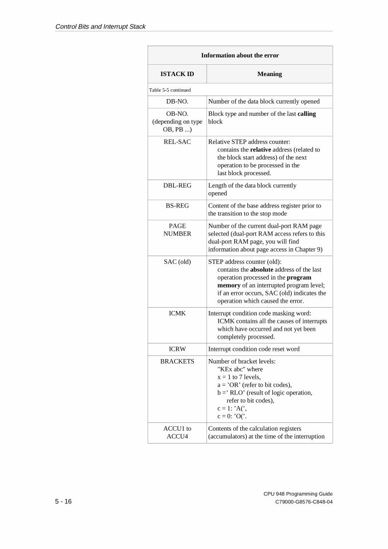
Information about the error
ISTACK ID Meaning
Table 5-5 continued
DB-NO. Number of the data block currently opened
OB-NO.(depending on type
OB, PB ...)
Block type and number of the last callingblock
REL-SAC Relative STEP address counter:contains the relative address (related tothe block start address) of the nextoperation to be processed in thelast block processed.
DBL-REG Length of the data block currentlyopened
BS-REG Content of the base address register prior tothe transition to the stop mode
PAGENUMBER
Number of the current dual-port RAM pageselected (dual-port RAM access refers to thisdual-port RAM page, you will findinformation about page access in Chapter 9)
SAC (old) STEP address counter (old):contains the absolute address of the lastoperation processed in the program memory of an interrupted program level; if an error occurs, SAC (old) indicates theoperation which caused the error.
ICMK Interrupt condition code masking word:ICMK contains all the causes of interruptswhich have occurred and not yet beencompletely processed.
ICRW Interrupt condition code reset word
BRACKETS Number of bracket levels: "KEx abc" where x = 1 to 7 levels,a = ’OR’ (refer to bit codes),b =’ RLO’ (result of logic operation,
refer to bit codes),c = 1: ’A(’,c = 0: ’O(’.
ACCU1 toACCU4
Contents of the calculation registers(accumulators) at the time of the interruption
Control Bits and Interrupt Stack
CPU 948 Programming Guide
5 - 16 C79000-G8576-C848-04
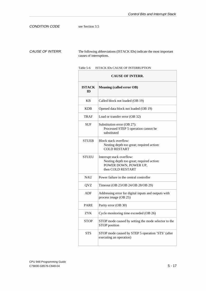
CONDITION CODE see Section 3.5
CAUSE OF INTERR. The following abbreviations (ISTACK IDs) indicate the most importantcauses of interruptions.
CAUSE OF INTERR.
ISTACK ID
Meaning (called error OB)
KB Called block not loaded (OB 19)
KDB Opened data block not loaded (OB 19)
TRAF Load or transfer error (OB 32)
SUF Substitution error (OB 27):Processed STEP 5 operation cannot be substituted
STUEB Block stack overflow:Nesting depth too great; required action:COLD RESTART
STUEU Interrupt stack overflow:Nesting depth too great; required action:POWER DOWN, POWER UP, then COLD RESTART
NAU Power failure in the central controller
QVZ Timeout (OB 23/OB 24/OB 28/OB 29)
ADF Addressing error for digital inputs and outputs withprocess image (OB 25)
PARE Parity error (OB 30)
ZYK Cycle monitoring time exceeded (OB 26)
STOP STOP mode caused by setting the mode selector to theSTOP position
STS STOP mode caused by STEP 5 operation ’STS’ (afterexecuting an operation)
Table 5-6 ISTACK IDs CAUSE OF INTERRUPTION
Control Bits and Interrupt Stack
CPU 948 Programming Guide
C79000-G8576-C848-04 5 - 17
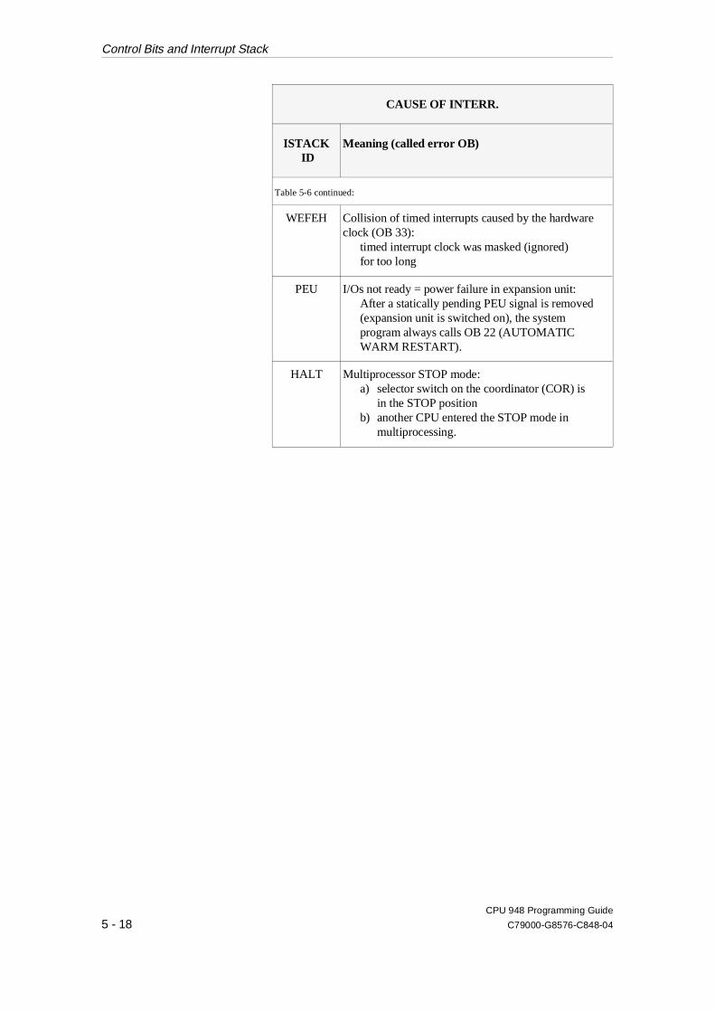
CAUSE OF INTERR.
ISTACK ID
Meaning (called error OB)
Table 5-6 continued:
WEFEH Collision of timed interrupts caused by the hardwareclock (OB 33):
timed interrupt clock was masked (ignored) for too long
PEU I/Os not ready = power failure in expansion unit:After a statically pending PEU signal is removed(expansion unit is switched on), the system program always calls OB 22 (AUTOMATIC WARM RESTART).
HALT Multiprocessor STOP mode:a) selector switch on the coordinator (COR) is
in the STOP positionb) another CPU entered the STOP mode in
multiprocessing.
Control Bits and Interrupt Stack
CPU 948 Programming Guide
5 - 18 C79000-G8576-C848-04

5.4.3Example of Error Diagnosisusing the ISTACK
Fig. 5-3 illustrates the structure of the ISTACK in conjunction with theinterruptions that have occurred.
- The program execution level CYCLE ( OB 1 ) is interrupted by an interrupt.- Following this, the program processing level interrupt is activated and OB 3 called.- The occurrence of a timed interrupt means that the INTERRUPT level is exited and the TIMED INTERRUPT level activated and OB 13 processed. - An incorrect addressing operation leads to the activaton of the ADF level where OB 25 is processed. In the error handling program, the user has programmed a stop operation (STS) the CPU aborts program execution.
Before the final transition to the stop mode, a total of four differentprogram execution levels were interrupted. If you now display the ISTACK onthe PG, you will obtain a four-level ISTACK, at the top the ISTACK withdepth 01, with the ID of the last interrupted program execution level (=ADF). You can page down through the ISTACK until you reach depth 04,representing the CYCLE program execution level, which was interrupted first .
STS
ADF
STS
X
X
Depth 04
Program execution levels ISTACK
Depth 03
Depth 02
Depth 01
CYCLE
TIMED INTERRUPTS
INTERRUPT
ADF
OB 1
OB 3
OB 13
OB 25
Fig. 5-3 Example of evaluating the ISTACK
Control Bits and Interrupt Stack
CPU 948 Programming Guide
C79000-G8576-C848-04 5 - 19

5.5 Error Handling Using Organization Blocks
When the system program detects an error, it calls the appropriateorganization block to handle it. You can determine further operation ofthe CPU by programming the appropriate organization block.Therefore, the CPU can do one of the following:
•• continue normal program processing
•• go into the STOP mode
and/or
•• process a special "error handling program"
For the following causes of error, OBs are available:
Cause of error Organizationblock called
Reaction of CPU if OB is not programmed
Call of a block that is not loaded (KB) OB 19 none
Attempt to open a data block DB/DX that is not loaded(KDB)
OB 19 STOP
Timeout in the user program during access to I/O peripherals(QVZ)
OB 23 none
Timeout during update of the process image table and duringinterprocessor communication flag transfer (QVZ)
OB 24 none
Addressing error (ADF) OB 25 STOP 1)
Cycle time exceeded (ZYK) OB 26 STOP
Substitution error (SUF) OB 27 STOP
Timeout by reading input byte IB 0 (process interrupts – QVZ)
OB 28 STOP
Timeout during access to the distributed I/O peripherals (extendedaddress area — QVZ)
OB 29 none
Parity error and timeout in the user memory (PARE) OB 30 STOP
Table 5-7 The organization blocks called in case of errors
Error Handling Using Organization Blocks
CPU 948 Programming Guide
5 - 20 C79000-G8576-C848-04

Cause of error Organizationblock called
Reaction of CPU if OB is not programmed
Table 5-7 continued:
Load and transfer error (TRAF) OB 32 STOP
Collision of timed interrupts:a) queue overflow (control bit WEFES)b) timed interrupt clock was masked (ignored) for too long
(WEFEH)
OB 33STOPnone
Error during STEP 5 operation "G DB/GX DX"(control bit FEDBX)
OB 34 STOP
Error in self-test (refer to Section 5.7) OB 36 none
1) The CPU changes to the STOP mode only if the addressing error is not disabled by the STEP 5 operation "IAE".
Examples of reactions toorganization blocks which arenot loaded
a) No reaction; cyclic program processing is not interrupted.
If a timeout error occurs and neither OB 23 nor OB 25 is loaded, cyclic program processing is notinterrupted according to the table above. The CPU does not react.If you want the CPU to go into the STOP mode when a timeout error occurs, you must enter a stopstatement (STP for STOP at cycle end) in the appropriate organization block (e.g. OB 23 with QVZ) andterminate it with the block end statement ’BE’.
Example of OB 23:: QVZ has occurred::STP Cyclic processing is aborted:BE CPU changes to the stop mode
b) Reaction : the CPU changes to the STOP mode.
The CPU changes to the STOP mode immediately when a corresponding error (e.g. cycle orload/transfer error) occurs - if you did not load the appropriate organization blocks.
If, as an exception, you do not want one of these errors to interrupt cyclic program processing (e.g. while putting the system into operation), a block end statement in the appropriate organization block is sufficient.
Example of OB 25:: ADF occurred::BE Cyclic processing is continued, no CPU STOP
Error Handling Using Organization Blocks
CPU 948 Programming Guide
C79000-G8576-C848-04 5 - 21

Interruptions duringprocessing of errororganization blocks
After the system program calls the appropriate organization block, theuser program in that block is processed.If another error occurs while that organization block is beingprocessed, the program is interrupted at the next operation boundaryand the appropriate organization block is called, just as in cyclicprogram processing.
The system program processes organization blocks in the order inwhich they are called.
NoteYou can nest a maximum of five error organization blocks. Withmore than 5 errors, the CPU goes into the HARD STOP modebecause of ISTACK overflow.
Error Handling Using Organization Blocks
CPU 948 Programming Guide
5 - 22 C79000-G8576-C848-04
5.6 Causes of Error and Reactions of the CPU
Specific events can interrupt cyclic, time-controlled, or interrupt-driven program processing at operation boundaries when the CPU isin the RUN mode.
During initialization and also in the RESTART mode, interruptionscan stop the start-up program and put the CPU into the STOP mode.The CPU then changes to the stop mode and calls the organizationblock for this particular error. Interruptions during the start-upprogram are handled like those in the RUN mode.
The reaction depends on the cause of the interruption:
•• immediate change to the STOP mode, without calling the error OB(e.g. NAU → hard stop, STUEU → hard stop, PEU → soft stop),
•• before changing to the STOP mode, the system program calls anerror OB which you can program and (depending on the cause ofthe error) avoid a change to the stop mode (e.g. QVZ/IB 0 →OB 28, ADF → OB 25).
If an error occurs, note the entries in the control bits under "Error IDs"and the entries in the ISTACK under CAUSE OF INTERR.
The following sections explain possible causes of error in greaterdetail.
Causes of Error and Reactions of the CPU
CPU 948 Programming Guide
C79000-G8576-C848-04 5 - 23

5.6.1OB 19: Calling a LogicBlock That Is Not Loaded(KB)
If your program jumps to a block that does not exist, the systemprogram detects an error. This applies to all logic blocks and also forconditional and unconditional calls.
When the system program detects the call of a logic block that isnot loaded, it calls OB 19, if this is loaded. In OB 19, you canspecify how the CPU should proceed.
If OB 19 does not exist, the system program continues executing theinterrupted STEP 5 program at the next operation.
5.6.2OB 19: Calling a Data BlockThat Is Not Loaded (KDB)
If you call a data block or an extended data block in your program thatdoes not exist in the memory or is marked as invalid, the CPU detectsan error and the system program calls OB 19, if this is loaded. IfOB 19 is not loaded, the CPU changes to the STOP mode. A zero isentered in the DBA and DBL registers.
NoteOB 19 is called both when a logic or data block is not loaded.You can read system data register RS 75 to determine (via theSTEP 5 program) which type of error occurred. The contents of RS 75 are as follows:- for a KB error: 0101H,- for a KDB error: 0904H.
Causes of Error and Reactions of the CPU
CPU 948 Programming Guide
5 - 24 C79000-G8576-C848-04
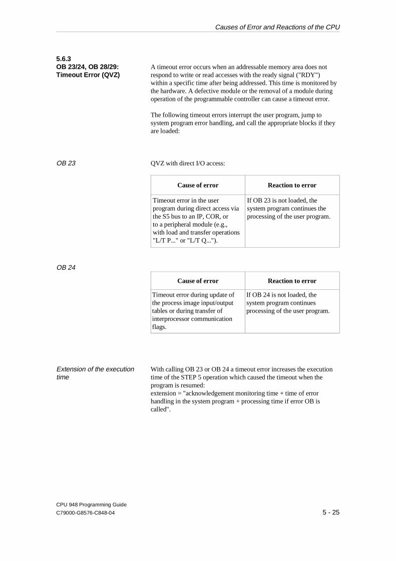
5.6.3OB 23/24, OB 28/29:Timeout Error (QVZ)
A timeout error occurs when an addressable memory area does notrespond to write or read accesses with the ready signal ("RDY")within a specific time after being addressed. This time is monitored bythe hardware. A defective module or the removal of a module duringoperation of the programmable controller can cause a timeout error.
The following timeout errors interrupt the user program, jump tosystem program error handling, and call the appropriate blocks if theyare loaded:
OB 23 QVZ with direct I/O access:
Cause of error Reaction to error
Timeout error in the userprogram during direct access viathe S5 bus to an IP, COR, orto a peripheral module (e.g.,with load and transfer operations "L/T P..." or "L/T Q...").
If OB 23 is not loaded, thesystem program continues theprocessing of the user program.
OB 24
Cause of error Reaction to error
Timeout error during update ofthe process image input/outputtables or during transfer ofinterprocessor communicationflags.
If OB 24 is not loaded, thesystem program continuesprocessing of the user program.
Extension of the executiontime
With calling OB 23 or OB 24 a timeout error increases the executiontime of the STEP 5 operation which caused the timeout when theprogram is resumed:extension = "acknowledgement monitoring time + time of errorhandling in the system program + processing time if error OB iscalled".
Causes of Error and Reactions of the CPU
CPU 948 Programming Guide
C79000-G8576-C848-04 5 - 25

OB 28
Cause of error Reaction to error
Timeout error at input byte IB 0(process interrupts)
If OB 28 is not loaded, the CPUchanges to the STOP mode.
OB 29
Cause of error Reaction to error
Timeout error of the distributedperipherals in the followingaddress areas:
- F 0000H to F EFFFH - F F200H to F FFFFH
If OB 29 is not loaded, thesystem program continuesprocessing of the user program.
Error address When a timeout error occurs, you can read the error address in thesystem data area (see Chapter 8):
RS Contents Address
68 QVZ error address high E F044H
69 QVZ error address low E F045H
5.6.4OB 25: AddressingError (ADF)
An addressing error occurs when a STEP 5 operation references aprocess image input or output to which no I/O module was assigned atthe time of the last COLD RESTART (the module is not plugged in, itis defective, or it is not defined in data block DB 1 of the CPU.
The STEP 5 operation at which the addressing error occurred isprocessed completely: For bit operations, the bit in the process imageis scanned and combined logically or set/reset. Load and transferoperations are also executed. Continued processing can, however,result in incorrect or unwanted reactions.
Causes of Error and Reactions of the CPU
CPU 948 Programming Guide
5 - 26 C79000-G8576-C848-04
When an addressing error occurs, the system program interruptsfurther processing of the user program and calls organization blockOB 25. After running the program contained in OB 25, the program isresumed at the next operation.If OB 25 is not loaded, the CPU changes to the STOP mode with anaddressing error.
The STEP 5 IAE operation disables addressing error monitoring forindividual program parts or for the entire program. You can enable itagain using the RAE operation (see Section 3.5.4 and List ofOperations).
5.6.5OB 26: Cycle TimeExceeded Error (ZYK)
The cycle time is the time between the start of one OB 1 and the next. It includes the entire duration of cyclic program processing includinginterrupts, interrupt servicing and system program activities. The cyclemonitoring time set on the CPU can, for example, be exceeded byincorrect programming (program loop).
NoteHardware faults as the cause of cycle time errors are extremelyrare. Normally, the error is in the user program or the programsand cycle monitoring time are incompatible.
When a cycle time exceeded error (ZYK) occurs, the system programinterrupts the user program and calls OB 26 if this is loaded. Themonitoring time is then restarted (triggered). If the monitoring time isexceeded again, before OB 26 is completed, the CPU changes to thestop mode.
If OB 26 is not loaded, the CPU changes to the STOP mode.
The cycle monitoring time is variable (10 to 2550 msec) and isretriggerable (see above).You can specify the cycle monitoring time individually by making anentry in DX 0 (refer to Chapter 7) or by programming OB 31. The defaultmonitoring time is 200 ms.
In the cyclic program, the cycle monitoring time can be retriggered bycalling the special function OB 222.
Causes of Error and Reactions of the CPU
CPU 948 Programming Guide
C79000-G8576-C848-04 5 - 27
5.6.6OB 27: (SubstitutionError SUF)
If an operation with a formal operand is to be carried out in a functionblock, the CPU replaces (substitutes) this formal operand with theactual operand in the block when the block is called during userprogram processing.
If the CPU detects an illegal substitution, it interrupts the userprogram and calls OB 27, if this is loaded. If OB 27 is not loaded, theCPU changes to the STOP mode.
Apart from an illegal substitution, SUF is also indicated in thefollowing situations:
•• illegal operation code,
•• special situation:you cannot open data blocks DB 0 and DB 1. The CPU handles theoperations "C DB 0" and "C DB 1" like substitution errors. A zerois entered in the DBA and DBL registers.
5.6.7OB 30: Parity Error and Timeout Error in the UserMemory (PARE)
The user memory is protected by a parity bit. The system programchecks whether the parity bit is correct each time the user memory isaccessed. If the parity bit is incorrectly set, a parity error is indicated.
The system program calls OB 30. If OB 30 is not loaded, the CPUchanges to the STOP mode.
The same reaction takes place if a timeout error occurs in the usermemory.
PARE accessing theoperating system RAM
If a parity error occurs when accessing the operating system RAM, thesystem program does not call OB 30, but changes to a HARD STOP.
Causes of Error and Reactions of the CPU
CPU 948 Programming Guide
5 - 28 C79000-G8576-C848-04
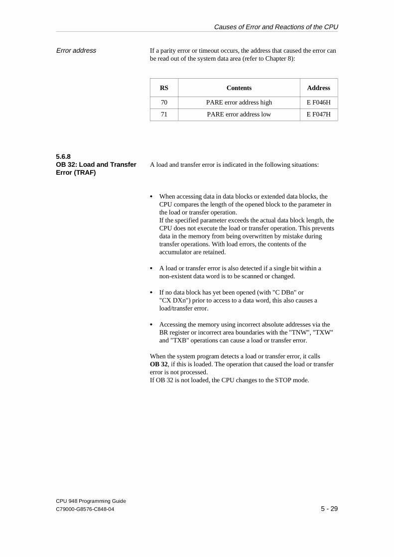
Error address If a parity error or timeout occurs, the address that caused the error canbe read out of the system data area (refer to Chapter 8):
RS Contents Address
70 PARE error address high E F046H
71 PARE error address low E F047H
5.6.8OB 32: Load and TransferError (TRAF)
A load and transfer error is indicated in the following situations:
•• When accessing data in data blocks or extended data blocks, theCPU compares the length of the opened block to the parameter inthe load or transfer operation. If the specified parameter exceeds the actual data block length, theCPU does not execute the load or transfer operation. This preventsdata in the memory from being overwritten by mistake duringtransfer operations. With load errors, the contents of theaccumulator are retained.
•• A load or transfer error is also detected if a single bit within anon-existent data word is to be scanned or changed.
•• If no data block has yet been opened (with "C DBn" or"CX DXn") prior to access to a data word, this also causes aload/transfer error.
•• Accessing the memory using incorrect absolute addresses via theBR register or incorrect area boundaries with the "TNW", "TXW"and "TXB" operations can cause a load or transfer error.
When the system program detects a load or transfer error, it callsOB 32, if this is loaded. The operation that caused the load or transfererror is not processed.If OB 32 is not loaded, the CPU changes to the STOP mode.
Causes of Error and Reactions of the CPU
CPU 948 Programming Guide
C79000-G8576-C848-04 5 - 29
5.6.9OB 33: Collision of TimedInterrupts Error(WEFES/WEFEH)
Time-controlled program processing (timed interrupts) is handled byorganization blocks OB 6, OB 9 and OB 10 to OB 18.
The following types of timed errors can occur on the CPU 948:
Queue overflow Cause:
Queue overflow servicing timed interrupts:
•• there are more than three timed interrupts pending for one of thethree shortest periods (OBs 10 to 12)
or
•• one of the other OBs (OBs 13 to 18) has been called before thefirst call was completely processed.
Reaction:
The system program calls OB 33 as the user interface, if this is loaded.You can program the reaction to this state in this OB.
If OB 33 is not loaded, the CPU changes to the STOP mode.
PG display in "OUTPUT ISTACK":
The bit WEFES is marked in the control bits.
Masking the timed interruptclock
Cause:
The internal timed interrupt clock is masked (ignored) too long(applies to interruptions at block boundaries/process interrupts).
This situation is related to the basic clock rate of the internal timedinterrupts and the scan time of a block in the cyclic user program. Ifthe scan of a cyclic block runs longer than the basic clock rate, acollision of timed interrupts occurs.
Causes of Error and Reactions of the CPU
CPU 948 Programming Guide
5 - 30 C79000-G8576-C848-04
Reaction:
The system program calls OB 33 as user interface, if this is loaded. Here, you can program the reaction to this state.
If OB 33 is not loaded, the CPU continues processing the program.
PG display with "OUTPUT ISTACK":
The bit WEFEH is marked in the control bits.
When the system program calls OB 33, a code for the collision oftimed interrupts is transferred to ACCU-1-L (see Section 4.5.3).
NoteIn the "process interrupt via IB 0" mode and "interruptability atblock boundaries" the step address counter (SAC) does not pointto the block at whose boundary (BE statement) the collision oftimed interrupts took place. It points to the block that called theblock that caused the error (return address).
As long as an error is pending or reoccurs every time the STEP 5operation in question is processed in each scan, the appropriateerror organization block is always called.
This can increase the cycle time considerably, depending on theduration of error handling by the system program and ofprocessing time of the organization block.
Causes of Error and Reactions of the CPU
CPU 948 Programming Guide
C79000-G8576-C848-04 5 - 31

5.6.10OB 34: Error with G DB/GX DX(FEDBX) Causes:
•• with the operation G DB/GX DX, an illegal block number wasspecified (number of a reserved block, number > 255),
•• with the operation G DB/GX DX, an illegal block length wasspecified (> 4091),
•• there is no longer enough space in the user memory for theoperation GDB/GXDX.
Reaction:
The system program calls OB 34 is this is loaded. If OB 34 is notloaded, the CPU changes to the stop mode.
5.6.11OB 35: CommunicationErrors
If problems occur on the second serial interface with an RK 512computer link, data transfer with procedure 3964/3964R, data transferwith an open driver or data transfer with SINEC L1, the systemprogram calls organization block OB 35 and enters additionalinformation about the error in ACCU 1.
Reaction if OB 35 is not loaded If you have not programmed OB 35, the system program does notreact and the CPU does not change to the STOP mode.
Error information in ACCU 1 The system program checks whether errors have occurred on the serialinterface every 100 ms. If an error has occurred, the system programenters error information in ACCU 1.
Error numbers for up to a maximum of three errors can be transferredwhen OB 35 is called. If there are more than three errors, this is indicatedby an overflow identifier.
Causes of Error and Reactions of the CPU
CPU 948 Programming Guide
5 - 32 C79000-G8576-C848-04

Structure of the errorinformation in ACCU 1
31 24 23 18 15 8 7 0
ACCU 1 0 0 0 0 F U B 0 Error number 1 Error number 2 Error number 3
F = ’0’, means no error entry= ’1’, means one or more errors entered
U = ’0’, means no error overflow (maximum three entries)= ‘1‘, means error overflow (more than three entries)
B = ’0’, means no BREAK on the interface= ’1’, means BREAK on the interface
BREAK If there is a BREAK on the interface, OB 35 is only called at thebeginning of the BREAK state.
Error number 1 to errornumber 3
Here, a maximum of three error numbers for errors detected on theinterface are entered in the order in which they were detected by thesystem.
Meaning of the error numbers The meaning of the error numbers and further information aboutdealing with interface errors can be found in the communicationmanual (Further Reading /14/).
5.6.12OB 36: Error in Self-test OB 36 is called if one of the self-test routines detects an error when it
is run (for detailed information, refer to Section 5.7).
Causes of Error and Reactions of the CPU
CPU 948 Programming Guide
C79000-G8576-C848-04 5 - 33
5.7 Self-Test
5.7.1Overview The CPU 948 contains integrated self-test routines in the system
program.
Activating/deactivating You can activate or deactivate the functions of the self-test using bitsin system data RS 137.
Time slice To reduce the cycle load caused by the self-test in the RUN mode,only part of the self-test is carried out within a cycle (time slice). Thetime available for the self-test can be set in RS 136 (refer toSection 5.7.3).
What can be tested? The self-test routines can carry out the following tests:
WHAT IS TESTED? WHEN?
The user memory During OVERALL RESET
The BASP signal (disable command output)
In the STOP mode
The hardware clock During COLD RESTART
The cycle time monitoring During START-UP
The address lines Cyclically in the RUN mode
The code of the system program(checksum)
Cyclically in the RUN mode
The code of the STEP 5 logicblocks in the user memory(checksum)
Cyclically in the RUN mode
Self-Test
CPU 948 Programming Guide
5 - 34 C79000-G8576-C848-04
5.7.2Description of the TestFunctions
Testing the user memory (During OVERALL RESET, without time slice)
The user memory is tested during an OVERALL RESET. This testchecks the user memory, the byte areas, the flags and process images.
During the test, the whole area (including the byte areas) are writtenwith a test pattern and then checked to make sure that they match. Atthe end of the test, the area is written with zeros.
NoteThe user memory test takes time to complete
- CPU 948-1 (640 Kbytes) approx. 5 seconds- CPU 948-2 (1 664 Kbytes) approx. 22 seconds
Testing the BASP signal (In the STOP mode, without time slice)
This test checks whether a BASP signal is output by the CPU. The testfunction runs in the stop loop. The BASP signal is then read cyclically.If an error is detected, an entry is made in the error buffer. At the nextSTART-UP, OB 36 (error in self-test) is called, if it exists. If OB 36 isloaded and contains an STP operation, the START-UP is aborted.Otherwise, the CPU changes to the cyclic mode.
Testing the hardware clock (During START-UP, however, only in CPU COLD RESTART ;without time slice)
This test is made before OB 20 is called and takes one second.
The current time is retained; existing timed jobs (clock-controlledinterrupts - OB 9) on the other hand are deleted.
Self-Test
CPU 948 Programming Guide
C79000-G8576-C848-04 5 - 35
Testing cycle time monitoring (During START-UP, without time slice)
With this function, the cycle time monitoring is checked during thestart-up phase. The cycle monitoring time is set to the minimum value(20 ms) and then a program loop started until the cycle error occurs.
Testing the address lines (Cyclically in RUN mode, with time slice)
In this test, wire breaks and short circuits on the address lines aredetected by writing test patterns via the lines, reading them back andcomparing them.
Testing the system programcode
(Cyclically in the RUN mode, with time slice)
In the operating code test, the content of the CPU operating system inthe internal RAM is checked (test area D 0000H to E 7FFDH).
The test is made by adding the content of the test area and thencomparing this with the checksum in the EPROM.
Testing the block code ofSTEP 5 logic blocks
(Cyclically in the RUN mode, with time slice)
The checksum of each valid STEP 5 logic block is checked.If a memory card is inserted, the checksum of the logic blocks of theCPU 948 is created following an OVERALL RESET and aftercopying the memory card contents to the internal user memory. Logicblocks added at a later point in time are also checked.
NoteIn the code test of the STEP 5 blocks, an error is detected if one ormore logic blocks were modified dynamically.It is possible to modify blocks with the PG. If this is the case, thechecksum is created by the system program of the CPU 948.
Self-Test
CPU 948 Programming Guide
5 - 36 C79000-G8576-C848-04
5.7.3Settings
Calculating and setting thenumber of time slices
The processing time for the self-functions is distributed on time sliceswhich are called once per cycle. The number of time slices can beselected. This means that you can increase the time required for theself-test functions per cycle.
Calculating the number First, you must estimate the time you can leave for the self-test withinthe cycle: the length of a time slice is approximately 500 µs, i.e. theself-test requires 500 µs in each cycle.
Once you have estimated how much time is available, you cancalculate the number of time slices each taking approximately 500 µs.
Setting the number You can set the number of time slices in system data word RS 136(16-bits wide). The default is 1 time slice (minimum value). You canset up to a maximum of 10 time slices (5 ms required in the cycle).
The number of time slices is derived from the value of system dataword RS 136 as follows:
RS 136 = 0 or 1: 1 time sliceRS 136 = 2: 2 time slicesRS 136 = 3: 3 time slicesetc.
Activating/deactivating thetests
You can activate the individual tests, e.g. in a start-up block, by settingthe corresponding bits in RS 137 to ’1’ and deactivate the tests bysetting the bits to ’0’.
NoteAfter an OVERALL RESET on a newly inserted CPU, all the testfunctions are switched off.The next time you make an OVERALL RESET, only the testfunctions to be run in the OVERALL RESET are activated. Allother test functions are deactivated.This means that you can only check the user memory of a newlyinserted CPU by activating the test function in RS 137 followingan OVERALL RESET and then repeating the OVERALL RESET.
Self-Test
CPU 948 Programming Guide
C79000-G8576-C848-04 5 - 37
Assignment of system dataword RS 137
Test function Bit no.
Check the code of the system program 2
Check the code of the STEP 5 logic blocks in theuser memory
5
Check the address lines 7
Check the clock 10
Check the BASP signal 11
Check the cycle time monitoring 13
Test the user memory 15
The bit numbers not listed in the table are not used.
5.7.4Error Handling Providing the test function is not running within an OVERALL
RESET, the test function calls error OB 36 (refer to Section 5.6.11) ifan error is detected and transfers the content of RS 137 containing thebits of the activated test routines to ACCU 1.
All the test routines also enter information about the type of test anderror detected in the system data words RS 75 to RS 78.
For test components which only run in an OVERALL RESET, thecause of the error is indicated in RS 75. The STOP LED then flashesquickly, when the tests are completed with an error in anOVERALL RESET .
Errors detected by the self-test component "BASP signal" in the STOPmode are also indicated in RS 75. The following START-UP onlyleads to cyclic operation if no STP operation is programmed inOB 36.
Self-Test
CPU 948 Programming Guide
5 - 38 C79000-G8576-C848-04
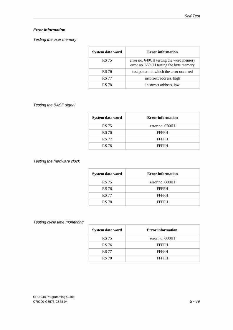
Error information
Testing the user memory
System data word Error information
RS 75 error no. 640CH testing the word memoryerror no. 650CH testing the byte memory
RS 76 test pattern in which the error occurred
RS 77 incorrect address, high
RS 78 incorrect address, low
Testing the BASP signal
System data word Error information
RS 75 error no. 6700H
RS 76 FFFFH
RS 77 FFFFH
RS 78 FFFFH
Testing the hardware clock
System data word Error information
RS 75 error no. 6800H
RS 76 FFFFH
RS 77 FFFFH
RS 78 FFFFH
Testing cycle time monitoring
System data word Error information.
RS 75 error no. 6600H
RS 76 FFFFH
RS 77 FFFFH
RS 78 FFFFH
Self-Test
CPU 948 Programming Guide
C79000-G8576-C848-04 5 - 39

Testing the address lines
System data word Error information
RS 75 error no. 630BH
RS 76 FFFFH
RS 77 incorrect address, high
RS 78 incorrect address, low
Testing the system programcode
System data word Error information
RS 75 error no. 610BH
RS 76 FFFFH
RS 77 actual checksum, high
RS 78 actual checksum, low
Testing the block code ofSTEP 5 logic blocks
System data word Error information
RS 75 error no. 620AH
RS 76 block type/block no. (IDs from block header)
RS 77 expected checksum
RS 78 actual checksum
Self-Test
CPU 948 Programming Guide
5 - 40 C79000-G8576-C848-04

Contents of Chapter 6
6.1 Introduction. . . . . . . . . . . . . . . . . . . . . . . . . . . . . . . . . . . . . . . . . . . . . . . . . . . . . . . . . . . . . 6 - 4
6.2 OB121: Set/Read System Time . . . . . . . . . . . . . . . . . . . . . . . . . . . . . . . . . . . . . . . . . . . . . 6 - 8
6.3 OB 122: "Disable Interrupts" On/Off . . . . . . . . . . . . . . . . . . . . . . . . . . . . . . . . . . . . . . . 6 - 12
6.4 OB 124: Delete STEP 5 Blocks . . . . . . . . . . . . . . . . . . . . . . . . . . . . . . . . . . . . . . . . . . . . 6 - 14
6.5 OB 125: Generate STEP 5 Blocks . . . . . . . . . . . . . . . . . . . . . . . . . . . . . . . . . . . . . . . . . . 6 - 17
6.6 OB 126: Define, Transfer Process Images. . . . . . . . . . . . . . . . . . . . . . . . . . . . . . . . . . . . 6 - 20
6.7 OB 129: Battery State. . . . . . . . . . . . . . . . . . . . . . . . . . . . . . . . . . . . . . . . . . . . . . . . . . . . 6 - 25
6.8 OB 131: Delete ACCUs 1, 2, 3 and 4 . . . . . . . . . . . . . . . . . . . . . . . . . . . . . . . . . . . . . . . 6 - 26
6.9 OB 132/133: Roll-Up ACCU/Roll-Down ACCU . . . . . . . . . . . . . . . . . . . . . . . . . . . . . . 6 - 27
6.10 OB 141: "Disable Single Cyclic Timed Interrupts" On/Off . . . . . . . . . . . . . . . . . . . . . . 6 - 29
6.11 OB 142: "Delay All Interrupts" On/Off . . . . . . . . . . . . . . . . . . . . . . . . . . . . . . . . . . . . . . 6 - 32
6.12 OB 143: "Delay Single Cyclic Timed Interrupts" On/Off . . . . . . . . . . . . . . . . . . . . . . . 6 - 35
6.13 OB 150: Set/Read System Time. . . . . . . . . . . . . . . . . . . . . . . . . . . . . . . . . . . . . . . . . . . . 6 - 38
6.14 OB 151: Set/Read Time for Clock-Controlled Interrupt. . . . . . . . . . . . . . . . . . . . . . . . . 6 - 43
6.15 OB 153: Set/Read Time for Delayed Interrupt . . . . . . . . . . . . . . . . . . . . . . . . . . . . . . . . 6 - 50
6.16 Ob 180: Variable Data Block Access . . . . . . . . . . . . . . . . . . . . . . . . . . . . . . . . . . . . . . . . 6 - 53
6Integrated Special Functions
CPU 948 Programming Guide
C79000-G8576-C848-04 6 - 1
6.17 OB 181: Test Data Blocks (DB/DX) . . . . . . . . . . . . . . . . . . . . . . . . . . . . . . . . . . . . . . . . 6 - 57
6.18 OB 182: Copy Data Area . . . . . . . . . . . . . . . . . . . . . . . . . . . . . . . . . . . . . . . . . . . . . . . . . 6 - 59
6.19 OB 202 to 205: Multiprocessor Communication . . . . . . . . . . . . . . . . . . . . . . . . . . . . . . 6 - 62
6.20 OB 222: Restart Cycle Monitoring Time. . . . . . . . . . . . . . . . . . . . . . . . . . . . . . . . . . . . . 6 - 63
6.21 OB 223: Compare Start-up Modes . . . . . . . . . . . . . . . . . . . . . . . . . . . . . . . . . . . . . . . . . 6 - 64
6.22 OB 254/255: Copy/Duplicate Data Blocks . . . . . . . . . . . . . . . . . . . . . . . . . . . . . . . . . . . 6 - 65
Contents
CPU 948 Programming Guide
6 - 2 C79000-G8576-C848-04
6Integrated Special Functions
The following chapter describes the special functions integrated in thesystem program, where you can use these functions and how to calland assign parameters to the special function OBs.You will also learn how to recognize errors in the execution of aspecial function and possible ways of handling them in the program.
CPU 948 Programming Guide
C79000-G8576-C848-04 6 - 3
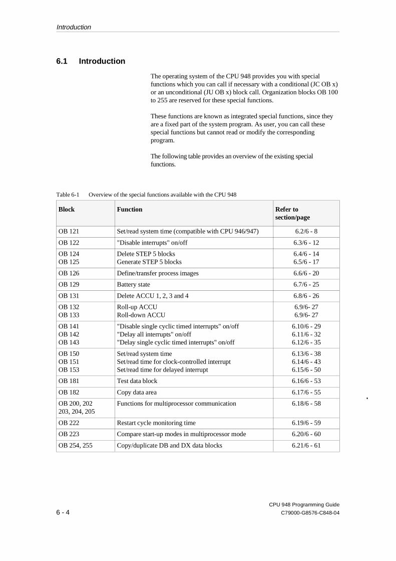
6.1 Introduction
The operating system of the CPU 948 provides you with specialfunctions which you can call if necessary with a conditional (JC OB x)or an unconditional (JU OB x) block call. Organization blocks OB 100to 255 are reserved for these special functions.
These functions are known as integrated special functions, since theyare a fixed part of the system program. As user, you can call thesespecial functions but cannot read or modify the correspondingprogram.
The following table provides an overview of the existing specialfunctions.
Block Function Refer tosection/page
OB 121 Set/read system time (compatible with CPU 946/947) 6.2/6 - 8
OB 122 "Disable interrupts" on/off 6.3/6 - 12
OB 124OB 125
Delete STEP 5 blocksGenerate STEP 5 blocks
6.4/6 - 146.5/6 - 17
OB 126 Define/transfer process images 6.6/6 - 20
OB 129 Battery state 6.7/6 - 25
OB 131 Delete ACCU 1, 2, 3 and 4 6.8/6 - 26
OB 132OB 133
Roll-up ACCURoll-down ACCU
6.9/6- 276.9/6- 27
OB 141OB 142OB 143
"Disable single cyclic timed interrupts" on/off"Delay all interrupts" on/off"Delay single cyclic timed interrupts" on/off
6.10/6 - 296.11/6 - 326.12/6 - 35
OB 150OB 151OB 153
Set/read system timeSet/read time for clock-controlled interruptSet/read time for delayed interrupt
6.13/6 - 386.14/6 - 436.15/6 - 50
OB 181 Test data block 6.16/6 - 53
OB 182 Copy data area 6.17/6 - 55
OB 200, 202203, 204, 205
Functions for multiprocessor communication 6.18/6 - 58
OB 222 Restart cycle monitoring time 6.19/6 - 59
OB 223 Compare start-up modes in multiprocessor mode 6.20/6 - 60
OB 254, 255 Copy/duplicate DB and DX data blocks 6.21/6 - 61
Table 6-1 Overview of the special functions available with the CPU 948
Introduction
CPU 948 Programming Guide
6 - 4 C79000-G8576-C848-04
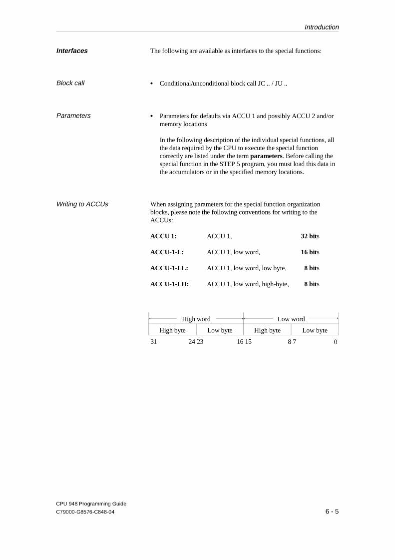
Interfaces The following are available as interfaces to the special functions:
Block call •• Conditional/unconditional block call JC .. / JU ..
Parameters •• Parameters for defaults via ACCU 1 and possibly ACCU 2 and/ormemory locations
In the following description of the individual special functions, allthe data required by the CPU to execute the special functioncorrectly are listed under the term parameters. Before calling thespecial function in the STEP 5 program, you must load this data inthe accumulators or in the specified memory locations.
Writing to ACCUs When assigning parameters for the special function organizationblocks, please note the following conventions for writing to theACCUs:
ACCU 1: ACCU 1, 32 bits
ACCU-1-L: ACCU 1, low word, 16 bits
ACCU-1-LL: ACCU 1, low word, low byte, 8 bits
ACCU-1-LH: ACCU 1, low word, high-byte, 8 bits
High word Low word
High byte Low byte High byte Low byte
31 24 23 16 15 8 7 0
Introduction
CPU 948 Programming Guide
C79000-G8576-C848-04 6 - 5
Error handling An error occurring in the execution of the active special function triggersa special error reaction in the system program.
In terms of this error reaction by the system program, two groups ofspecial functions can be distinguished.
•• Group 1:
ACCU condition code bits Group 1 includes all the special functions with which IDs aretransferred to ACCU 1 if an error occurs to further explain theerror.
•• Group 2:
RLO ,CC0/CC1
With some of the special functions, the RLO or the status bitsCC0/CC1 are written to indicate errors for specific specialfunctions.If an error occurs when using one of these special functions, theRLO is set to "1" in most cases. In your STEP 5 program, you canuse a JC operation (conditional jump) to evaluate the RLO forthese special functions and then react to an error.
In some special functions, the results bits CC0 and CC1 areaffected by the processing of a special function. You can scanthese bits in your STEP 5 program using a compare operation andonce again program a reaction to an error.
Which of the error reactions occurs for the individual special functionOBs is explained in the following sections.
Introduction
CPU 948 Programming Guide
6 - 6 C79000-G8576-C848-04
NoteCalling a special function OB using the "JU OB 131/132/133" or"JC OB 131/132/133" operation does not have the same effect asa "genuine" block change, but functions as a STEP 5 operationwithout block operand. No interrupts are nested (with the default"interrupts at block boundaries").
Introduction
CPU 948 Programming Guide
C79000-G8576-C848-04 6 - 7

6.2 OB 121: Set/Read System Time
Function With OB121 you can set or read the system time (date and time). Thisfunction is compatible with the CPU 946/947.
Parameters 1. Data field
Four words in the word-oriented memory area.With the "set system time" function the area before the OB121 callmust be loaded with the time values to be set. The system programchecks these values to ensure they are logically correct.With the "read system time" function, OB121 enters the current timevalues in this area.
Structure of the data field
Bit no. 15 12 11 9 8 4 3 0
1st word Sec. x 10 Sec. x 1 10th Sec. 100th Sec.
2ndword Hour x 10 Hour x 1 Min. x 10 Min x 1
3rd word Day x 10 Day x 1 Weekday 0
4th word Year x 10 Year x 1 Month x 10 Month x 1
NoteThe structure of the data field corresponds to the structure ofsystem data RS 96 to RS 99 (current time).
Possible time values:
100th seconds: 0 to 910th seconds: 0 to 9
Seconds x 1: 0 to 9Seconds x 10: 0 to 5
Minutes x 1: 0 to 9Minutes x 10: 0 to 5
Hours x 1: 0 to 9Hours x 10:
Bit no. 12 /13: 0 to 1 with 12 hour format
0 to 2 with 24 hour formatBit no. 14: 0 = AM with 12 hour format
1 = PM " "0 in 24 hour format
Bit no. 15: 0 = 12 hour format1 = 24 hour format
OB 121: Set/Read System Time
CPU 948 Programming Guide
6 - 8 C79000-G8576-C848-04
Weekday: 0 to 6 for Mon to Sun
Days x 1: 0 to 9Days x 10: 0 to 3
Month x 1: 0 to 9Month x 10: 0 to 1
Year x 1: 0 to 9Year x 10: 0 to 9
2. BR register (base address register)
Start address of a data field in an area of memory organized in words,from which the time values to be set are read or in which the currenttime values are to be stored. The BR register must be loaded with theaddress before the OB 121 call.
3. ACCU-1-L
Function no.,Permitted values: 1 = set system time
2 = read system time
Result After correct and error-free processing, the system program enters thevalue ’0’ in ACCU-1-L. After the "set" function, the system time is setto the values contained in the data field; after the "read" function, thedata field contains the current time values.
Possible errors The errors listed in the following table can occur. If one of these errorsdoes occur, the system program enters the error ID shown in the tablein ACCU-1-L.
ID Meaning
F001HF00FHF101HF102HF103HF104HF105HF106HF107HF108H
F109H
Illegal function no.Multiple block callYear specification illegalMonth specification illegalDay specification illegalWeekday specification illegalHour specification illegalMinute specification illegalSeconds specification illegal100th to 10th seconds in the data field unequal to 0.Entries from the 100th to the 10th second mustequal 0.Hour format differs from setting in OB 151
Table 6-2 Error IDs of OB 121 in ACCU-1-L
OB 121: Set/Read System Time
CPU 948 Programming Guide
C79000-G8576-C848-04 6 - 9

Examples
Programming example for "set system time"
FB 13 is programmed for the "set system time" function. The new values aretransferred in data block DB 10 (data word DW 0 to DW 3).
STEP 5 program:
FB13NAME :CLKWR
:C DB 10 Open DB 10:L KH 1500 15 seconds (10th .. 100th sec. = 0!):T DW 0:L KH 9555 24 hour mode, 15 hours 55 minutes:T DW 1:L KH 1010 the 10th, Tuesday:T DW 2:L KH 9308 1993, August:T DW 3:MBR EEC00 Load start address of the DB list: in the BR:LRW +10 Load the start address of DB 10 in memory: (paragraph address) in ACCU 1:SLD 4 Absolute address of DB 10 (DW 0):MAB Load content of ACCU 1 into BR register:L KB 1 Load function no. ’1’ in ACCU-1-L:JU OB 121 Set system time:L KB 0:><F Scan error bits:JC =ERRO Jump to error handling:BEU:
ERRO : Error handling::BE
Data block DB 10 contains the following information when OB 121 is called:
0: KH = 1500;1: KH = 9555;2: KH = 1010;3: KH = 9308;4:
OB 121 transfers the required time parameters from DB 10 to the system dataarea RS 96 to RS 99.
OB 121: Set/Read System Time
CPU 948 Programming Guide
6 - 10 C79000-G8576-C848-04
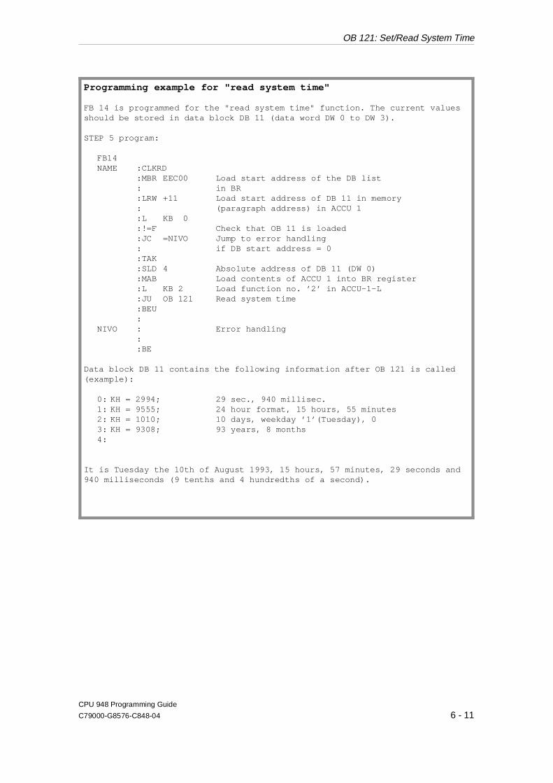
Programming example for "read system time"
FB 14 is programmed for the "read system time" function. The current valuesshould be stored in data block DB 11 (data word DW 0 to DW 3).
STEP 5 program:
FB14NAME :CLKRD
:MBR EEC00 Load start address of the DB list: in BR:LRW +11 Load start address of DB 11 in memory: (paragraph address) in ACCU 1:L KB 0:!=F Check that OB 11 is loaded:JC =NIVO Jump to error handling: if DB start address = 0:TAK:SLD 4 Absolute address of DB 11 (DW 0):MAB Load contents of ACCU 1 into BR register:L KB 2 Load function no. ’2’ in ACCU-1-L:JU OB 121 Read system time:BEU:
NIVO : Error handling::BE
Data block DB 11 contains the following information after OB 121 is called(example):
0: KH = 2994; 29 sec., 940 millisec.1: KH = 9555; 24 hour format, 15 hours, 55 minutes2: KH = 1010; 10 days, weekday ’1’(Tuesday), 03: KH = 9308; 93 years, 8 months4:
It is Tuesday the 10th of August 1993, 15 hours, 57 minutes, 29 seconds and940 milliseconds (9 tenths and 4 hundredths of a second).
OB 121: Set/Read System Time
CPU 948 Programming Guide
C79000-G8576-C848-04 6 - 11

6.3 OB 122: "Disable Interrupts" On/Off
A STEP 5 program can be interrupted at block boundaries or operationboundaries by programs at an execution level with a higher priority.The program execution levels with higher priority include thefollowing:
•• TIMED INTERRUPTS
and
•• PROCESS INTERRUPTS.
The time required to run the interrupted programs is expanded by therun time of the nested programs.
Function Using OB 122, you can prevent interrupt servicing blocks beingnested at one or more consecutive block or operation boundaries.
OB 122 influences the acceptance of interrupts:
•• "Disable interrupts" on means the following:no interrupts will be registered from now on.
•• "Disable interrupts" off means the following:all interrupts occurring will be registered from now on and thecorresponding blocks will be nested and executed at the nextoperation or block boundary (depending on the mode set in DX 0).
Interrupts that have already been registered, are then no longerserviced if the mode "interruptability at block boundaries" is set inDX 0.
Parameters ACCU-1-L
Function no.,Permitted values: 1 = disable all interrupts
2 = enable all interrupts
OB 122: "Disable Interrupts" On/Off
CPU 948 Programming Guide
6 - 12 C79000-G8576-C848-04

Result After correct and error-free processing, the system program enters thevalue ’0’ in ACCU-1-L.
NoteBy calling OB 122, the RLO (undefined) is influenced. The BRregister is not modified.To disable and enable processing interrupts, you can also use theSTEP 5 operations IA and RA instead of OB 122. The blocking ofinterrupts is cleared at the next system checkpoint (refer toChapter 11).
Possible errors The errors listed in the following table can occur. If one of these errordoes occur, the system program writes the error ID shown in the tableinto ACCU-1-L.
ID Meaning
F001H Illegal function number
Example
Table 6-3 Error IDs of OB 122 in ACCU-1-L
Excerpt of a STEP 5 program in which allinterrupts are disabled using OB 122 immediatelybefore a critical program section following whichthey are enabled again:
:L KB 1 Load function ID in ACCU-1-L:JU OB 122 Disable all interrupts: ): ): ): } Critical program section: ): ):L KB 2 Load function ID in ACCU-1-L:JU OB 122 Enable all interrupts::
OB 122: "Disable Interrupts" On/Off
CPU 948 Programming Guide
C79000-G8576-C848-04 6 - 13

6.4 OB 124: Delete STEP 5 Blocks
Function With OB 24, you can delete any STEP 5 blocks (logic and datablocks) in the user memory. The deleted block is removed from theaddress list in DB 0. The gap in memory resulting from deleting a block is used again whennew blocks are loaded.
Parameters 1. ACCU-1-LH
Block type of the block to be deleted
2. ACCU-1-LL
Block number of the block to be deleted
Permitted block types and numbers:
ACCU-1-LH (block type) ACCU-1-LL ( block number)
1 = PB2 = SB3 = FB4 = FX5 = DB6 = DX7 = OB
0 to 2550 to 2550 to 2550 to 2553 to 2553 to 2551 to 39
Result After correct and error-free processing, the system program sets theRLO to ’0’ and clears the condition codes CC 1 and CC 0.
NoteWhile the blocks are actually being deleted, user interrupts aredisabled: no interrupts come through.
By calling OB 124, the contents of ACCU 1 to ACCU 4 aremodified. The BR register is retained.
OB 124: Delete STEP 5 Blocks
CPU 948 Programming Guide
6 - 14 C79000-G8576-C848-04

Possible errors andwarnings
If an error or warning occurs, the system program stops processingOB 124 and continues program execution at the next STEP 5operation. It also sets the RLO to ’1’ and writes an ID to ACCU-1-LL(refer to Table 6-5).
If the function is aborted with a warning, it may be possible to achievecorrect execution of OB 124 by re-calling the special function(possibly several times).
In the following case, OB 124 is aborted with a warning:
During the last 10 ms OB 124, OB 125, OB 254 or OB 255 has beencalled. (Only one call for these special functions is allowed within10 ms. This avoids multiple calls for the OBs listed above blockingthe interface to the PG so that it can no longer be processed.)
Condition code bits After calling OB 124, you can check whether the special function hasbeen executed correctly or was aborted with an "error" or "warning"using the result of logic operation and the condition code bits CC 1and CC 0. The result can be evaluated with conditional jumpoperations.
Results bits
RLO CC 1 CC 0 Meaning Scan
0 0 0 Special function wasprocessed correctly
JCJZ
1 1 0 Processing of specialfunction aborted with"warning"
JCJPJN
1 0 1 Processing of specialfunction aborted with "error"
JCJMJN
Table 6-4 Results bits of OB 124
OB 124: Delete STEP 5 Blocks
CPU 948 Programming Guide
C79000-G8576-C848-04 6 - 15
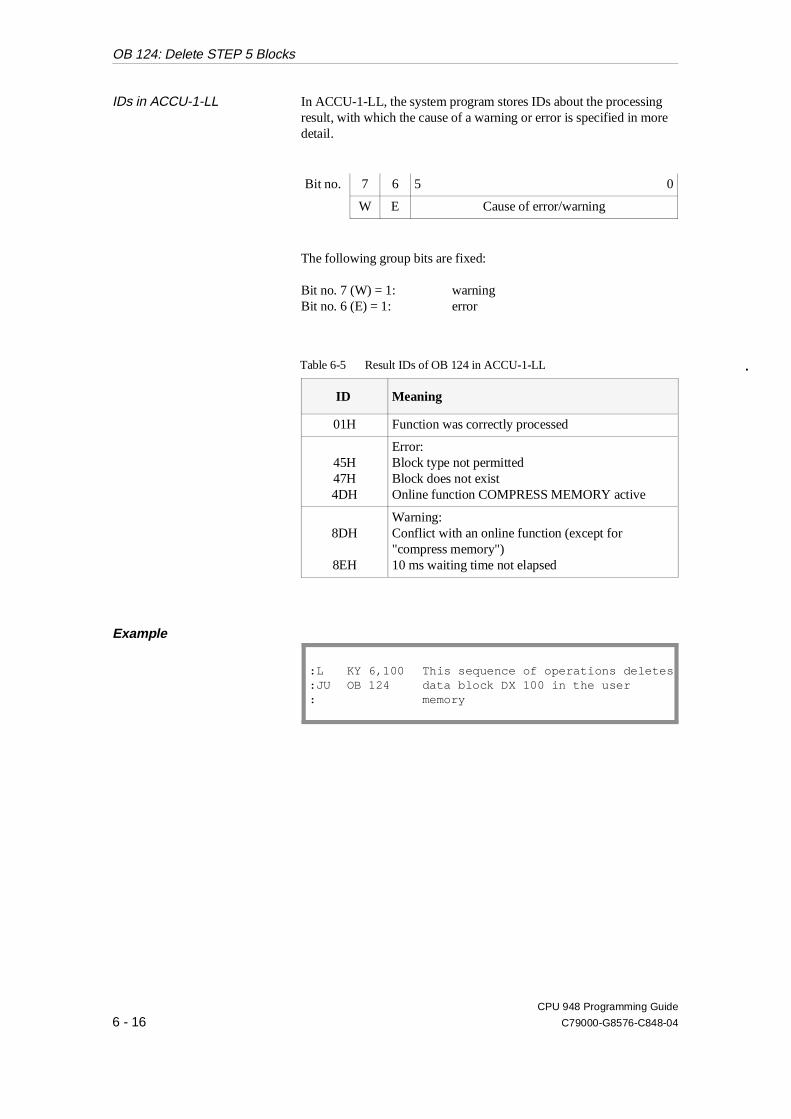
IDs in ACCU-1-LL In ACCU-1-LL, the system program stores IDs about the processingresult, with which the cause of a warning or error is specified in moredetail.
Bit no. 7 6 5 0
W E Cause of error/warning
The following group bits are fixed:
Bit no. 7 (W) = 1: warningBit no. 6 (E) = 1: error
ID Meaning
01H Function was correctly processed
45H47H4DH
Error:Block type not permittedBlock does not existOnline function COMPRESS MEMORY active
8DH
8EH
Warning:Conflict with an online function (except for"compress memory")10 ms waiting time not elapsed
Example
Table 6-5 Result IDs of OB 124 in ACCU-1-LL
:L KY 6,100 This sequence of operations deletes :JU OB 124 data block DX 100 in the user: memory
OB 124: Delete STEP 5 Blocks
CPU 948 Programming Guide
6 - 16 C79000-G8576-C848-04
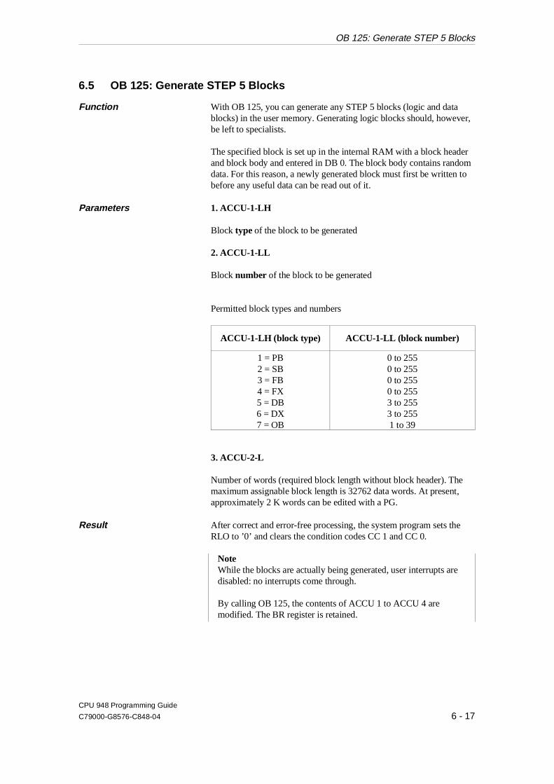
6.5 OB 125: Generate STEP 5 Blocks
Function With OB 125, you can generate any STEP 5 blocks (logic and datablocks) in the user memory. Generating logic blocks should, however,be left to specialists.
The specified block is set up in the internal RAM with a block headerand block body and entered in DB 0. The block body contains randomdata. For this reason, a newly generated block must first be written tobefore any useful data can be read out of it.
Parameters 1. ACCU-1-LH
Block type of the block to be generated
2. ACCU-1-LL
Block number of the block to be generated
Permitted block types and numbers
ACCU-1-LH (block type) ACCU-1-LL ( block number)
1 = PB2 = SB3 = FB4 = FX5 = DB6 = DX7 = OB
0 to 2550 to 2550 to 2550 to 2553 to 2553 to 2551 to 39
3. ACCU-2-L
Number of words (required block length without block header). Themaximum assignable block length is 32762 data words. At present,approximately 2 K words can be edited with a PG.
Result After correct and error-free processing, the system program sets theRLO to ’0’ and clears the condition codes CC 1 and CC 0.
NoteWhile the blocks are actually being generated, user interrupts aredisabled: no interrupts come through.
By calling OB 125, the contents of ACCU 1 to ACCU 4 aremodified. The BR register is retained.
OB 125: Generate STEP 5 Blocks
CPU 948 Programming Guide
C79000-G8576-C848-04 6 - 17
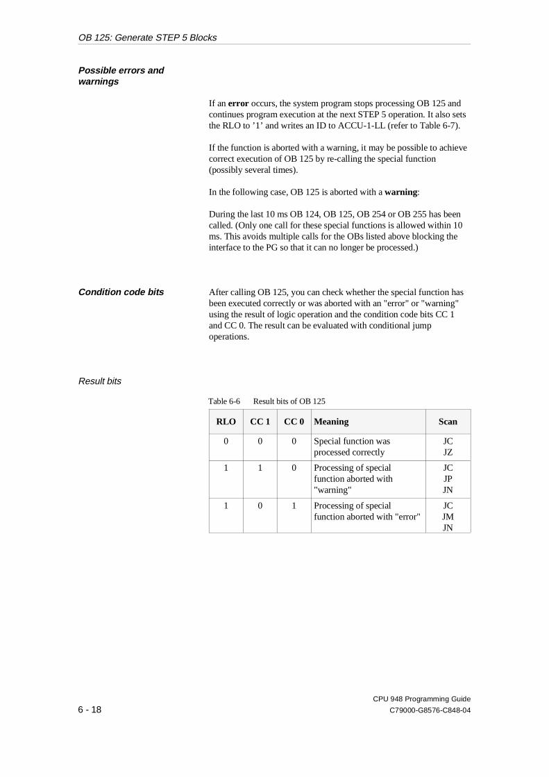
Possible errors andwarnings
If an error occurs, the system program stops processing OB 125 andcontinues program execution at the next STEP 5 operation. It also setsthe RLO to ’1’ and writes an ID to ACCU-1-LL (refer to Table 6-7).
If the function is aborted with a warning, it may be possible to achievecorrect execution of OB 125 by re-calling the special function(possibly several times).
In the following case, OB 125 is aborted with a warning:
During the last 10 ms OB 124, OB 125, OB 254 or OB 255 has beencalled. (Only one call for these special functions is allowed within 10ms. This avoids multiple calls for the OBs listed above blocking theinterface to the PG so that it can no longer be processed.)
Condition code bits After calling OB 125, you can check whether the special function hasbeen executed correctly or was aborted with an "error" or "warning"using the result of logic operation and the condition code bits CC 1and CC 0. The result can be evaluated with conditional jumpoperations.
Result bits
RLO CC 1 CC 0 Meaning Scan
0 0 0 Special function wasprocessed correctly
JCJZ
1 1 0 Processing of specialfunction aborted with"warning"
JCJPJN
1 0 1 Processing of specialfunction aborted with "error"
JCJMJN
Table 6-6 Result bits of OB 125
OB 125: Generate STEP 5 Blocks
CPU 948 Programming Guide
6 - 18 C79000-G8576-C848-04
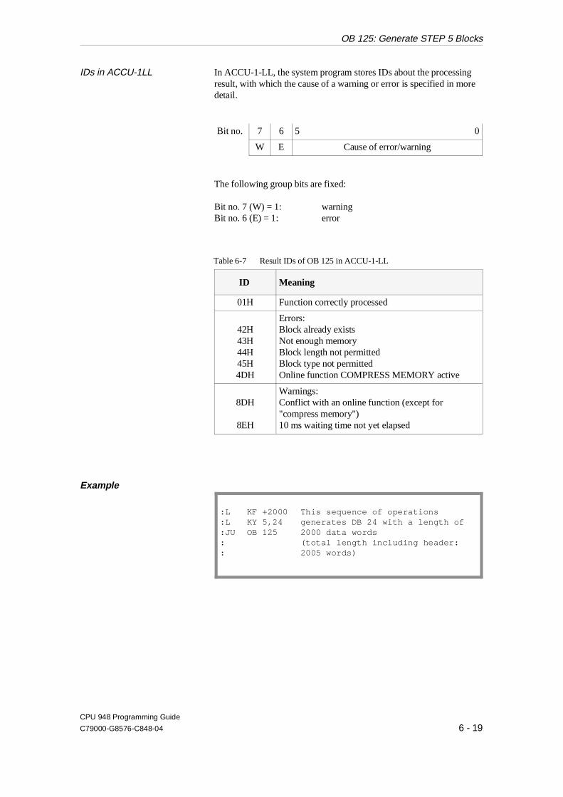
IDs in ACCU-1LL In ACCU-1-LL, the system program stores IDs about the processingresult, with which the cause of a warning or error is specified in moredetail.
Bit no. 7 6 5 0
W E Cause of error/warning
The following group bits are fixed:
Bit no. 7 (W) = 1: warningBit no. 6 (E) = 1: error
ID Meaning
01H Function correctly processed
42H43H44H45H4DH
Errors:Block already existsNot enough memoryBlock length not permittedBlock type not permittedOnline function COMPRESS MEMORY active
8DH
8EH
Warnings:Conflict with an online function (except for"compress memory")10 ms waiting time not yet elapsed
Example
Table 6-7 Result IDs of OB 125 in ACCU-1-LL
:L KF +2000 This sequence of operations :L KY 5,24 generates DB 24 with a length of:JU OB 125 2000 data words: (total length including header: : 2005 words)
OB 125: Generate STEP 5 Blocks
CPU 948 Programming Guide
C79000-G8576-C848-04 6 - 19

6.6 OB 126: Define, Transfer Process Images
Each time the cycle is run through, the system program updates theprocess image of the digital inputs and outputs and IPC flags. Theinputs, outputs and IPC flags included in the process image are storedin system data block DB 1 (refer to Chapter 10).With OB 126, you can use additional process images.
Function Using OB 126, you can program up to four further process images inaddition to the process image in DB 1 during a COLD RESTART .These additional process images can be read in and output with theSTEP 5 program at any program execution level.
Parameters 1. Data field
6 flags with the following structure:
Bit no. 7 0
FY n Function no.
FY n+1 Address list no.
FY n+2 Block type
FY n+3 Block number
FY n+4 Data word no. of the first ID word
FY n+5 in the address list
Parameters of the data field:
Function no. With the function number, you stipulate which job OB 126 is toperform (refer to the table).
Permitted values: 1 to 5
Function no. Function
1234
Read in the process image of the digital inputsOutput the process image of the digital outputsRead in the process image of the IPC input flagsOutput the process image of the IPC output flags
5 Set up system internal address list (analogous toDB 1)
(only permitted in COLD RESTART OB 20)
OB 126: Define, Transfer Process Images
CPU 948 Programming Guide
6 - 20 C79000-G8576-C848-04
Address list number Number of the address list for the additionally defined process image;
permitted values: 1 to 4
Block type Type of data block containing the address list;
permitted values: 1 = DB2 = DX
Block number Number of the data block containing the address list;
permitted values: 3 to 255
DW no. 1st ID word Here, you enter the number of the data word in which the first IDword of the address list is located (refer to structure of DB 1,Section 10.1.6).The following ID words are possible:
KH = DE00 (digital inputs)KH = DA00 (digital outputs)KH = CE00 (IPC input flags)KH = CA00 (IPC output flags)
The parameter occupies 2 flag bytes!
NoteThe complete data field only needs to be set up when OB 26 is togenerate the address list during a COLD RESTART (= function5). To execute functions 1 to 4 it is adequate to simply enter theaddress list number alongside the function number in the datafield. The remaining entries are then not needed.
You must structure the data block with which you want to set upthe address list for an additional process image (= function 5)analogous to DB 1.You can store the address list information for each of theadditional process images in this data block by adding an end IDto each field of information as in DB 1.To set up the address list, you must however call OB 126 for eachadditional process image using function "5" singly (only in COLDRESTART).
2. ACCU-1-L
No. of the flag byte FY n, at which the data field begins
permitted values: 0 to 250
OB 126: Define, Transfer Process Images
CPU 948 Programming Guide
C79000-G8576-C848-04 6 - 21
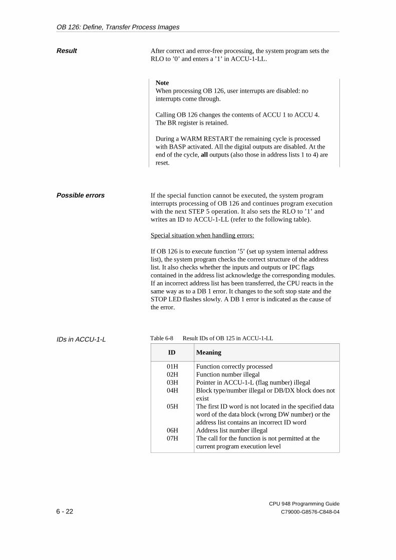
Result After correct and error-free processing, the system program sets theRLO to ’0’ and enters a ’1’ in ACCU-1-LL.
NoteWhen processing OB 126, user interrupts are disabled: nointerrupts come through.
Calling OB 126 changes the contents of ACCU 1 to ACCU 4.The BR register is retained.
During a WARM RESTART the remaining cycle is processedwith BASP activated. All the digital outputs are disabled. At theend of the cycle, all outputs (also those in address lists 1 to 4) arereset.
Possible errors If the special function cannot be executed, the system programinterrupts processing of OB 126 and continues program executionwith the next STEP 5 operation. It also sets the RLO to ’1’ andwrites an ID to ACCU-1-LL (refer to the following table).
Special situation when handling errors:
If OB 126 is to execute function ’5’ (set up system internal addresslist), the system program checks the correct structure of the addresslist. It also checks whether the inputs and outputs or IPC flagscontained in the address list acknowledge the corresponding modules.If an incorrect address list has been transferred, the CPU reacts in thesame way as to a DB 1 error. It changes to the soft stop state and theSTOP LED flashes slowly. A DB 1 error is indicated as the cause ofthe error.
IDs in ACCU-1-L
ID Meaning
01H02H03H04H
05H
06H07H
Function correctly processedFunction number illegalPointer in ACCU-1-L (flag number) illegalBlock type/number illegal or DB/DX block does notexistThe first ID word is not located in the specified dataword of the data block (wrong DW number) or theaddress list contains an incorrect ID wordAddress list number illegalThe call for the function is not permitted at thecurrent program execution level
Table 6-8 Result IDs of OB 125 in ACCU-1-LL
OB 126: Define, Transfer Process Images
CPU 948 Programming Guide
6 - 22 C79000-G8576-C848-04
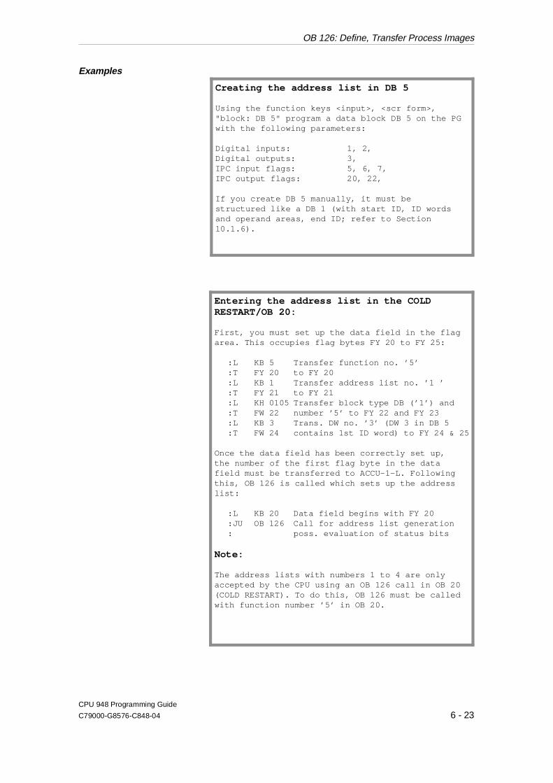
Examples
Creating the address list in DB 5
Using the function keys <input>, <scr form>,"block: DB 5" program a data block DB 5 on the PGwith the following parameters:
Digital inputs: 1, 2, Digital outputs: 3,IPC input flags: 5, 6, 7,IPC output flags: 20, 22,
If you create DB 5 manually, it must bestructured like a DB 1 (with start ID, ID wordsand operand areas, end ID; refer to Section10.1.6).
Entering the address list in the COLDRESTART/OB 20:
First, you must set up the data field in the flagarea. This occupies flag bytes FY 20 to FY 25:
:L KB 5 Transfer function no. ’5’:T FY 20 to FY 20:L KB 1 Transfer address list no. ’1 ’:T FY 21 to FY 21:L KH 0105 Transfer block type DB (’1’) and:T FW 22 number ’5’ to FY 22 and FY 23:L KB 3 Trans. DW no. ’3’ (DW 3 in DB 5:T FW 24 contains 1st ID word) to FY 24 & 25
Once the data field has been correctly set up,the number of the first flag byte in the datafield must be transferred to ACCU-1-L. Followingthis, OB 126 is called which sets up the addresslist:
:L KB 20 Data field begins with FY 20:JU OB 126 Call for address list generation: poss. evaluation of status bits
Note:
The address lists with numbers 1 to 4 are onlyaccepted by the CPU using an OB 126 call in OB 20(COLD RESTART). To do this, OB 126 must be calledwith function number ’5’ in OB 20.
OB 126: Define, Transfer Process Images
CPU 948 Programming Guide
C79000-G8576-C848-04 6 - 23
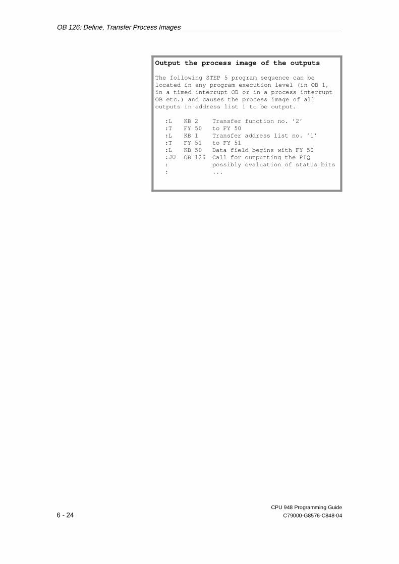
Output the process image of the outputs
The following STEP 5 program sequence can belocated in any program execution level (in OB 1,in a timed interrupt OB or in a process interruptOB etc.) and causes the process image of alloutputs in address list 1 to be output.
:L KB 2 Transfer function no. ’2’:T FY 50 to FY 50:L KB 1 Transfer address list no. ’1’ :T FY 51 to FY 51:L KB 50 Data field begins with FY 50:JU OB 126 Call for outputting the PIQ: possibly evaluation of status bits: ...
OB 126: Define, Transfer Process Images
CPU 948 Programming Guide
6 - 24 C79000-G8576-C848-04
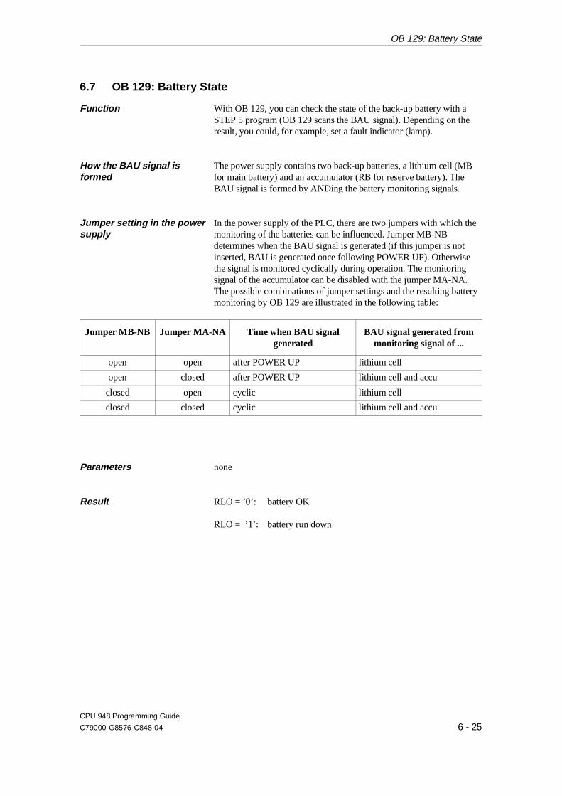
6.7 OB 129: Battery State
Function With OB 129, you can check the state of the back-up battery with aSTEP 5 program (OB 129 scans the BAU signal). Depending on theresult, you could, for example, set a fault indicator (lamp).
How the BAU signal isformed
The power supply contains two back-up batteries, a lithium cell (MBfor main battery) and an accumulator (RB for reserve battery). TheBAU signal is formed by ANDing the battery monitoring signals.
Jumper setting in the powersupply
In the power supply of the PLC, there are two jumpers with which themonitoring of the batteries can be influenced. Jumper MB-NBdetermines when the BAU signal is generated (if this jumper is notinserted, BAU is generated once following POWER UP). Otherwisethe signal is monitored cyclically during operation. The monitoringsignal of the accumulator can be disabled with the jumper MA-NA.The possible combinations of jumper settings and the resulting batterymonitoring by OB 129 are illustrated in the following table:
Jumper MB-NB Jumper MA-NA Time when BAU signalgenerated
BAU signal generated frommonitoring signal of ...
open open after POWER UP lithium cell
open closed after POWER UP lithium cell and accu
closed open cyclic lithium cell
closed closed cyclic lithium cell and accu
Parameters none
Result RLO = ’0’: battery OK
RLO = ’1’: battery run down
OB 129: Battery State
CPU 948 Programming Guide
C79000-G8576-C848-04 6 - 25

Example
6.8 OB 131: Delete ACCUs 1, 2, 3 and 4
Function By calling special function organization block OB 131 once, you candelete the contents of ACCUs 1 to 4 extremely simply. OB 131overwrites all four registers with ’0’.
Parameters None
Result The ACCUs 1 to 4 (each 32 bit) are deleted (’0’).
Possible errors None
With the following sequence of operations, youcan check whether or not the battery is OK and ifit is not, you can energize a lamp:
::JU OB 129:JC =BATL RLO = 1 -> battery run down:::BEU
BATL :SU Q 22.5 switch on warning lamp at: output byte 22, bit 5:BE
OB 131: Delete ACCUs 1, 2, 3 and 4
CPU 948 Programming Guide
6 - 26 C79000-G8576-C848-04
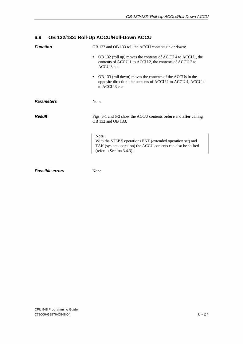
6.9 OB 132/133: Roll-Up ACCU/Roll-Down ACCU
Function OB 132 and OB 133 roll the ACCU contents up or down:
•• OB 132 (roll up) moves the contents of ACCU 4 to ACCU1, thecontents of ACCU 1 to ACCU 2, the contents of ACCU 2 toACCU 3 etc.
•• OB 133 (roll down) moves the contents of the ACCUs in theopposite direction: the contents of ACCU 1 to ACCU 4, ACCU 4to ACCU 3 etc.
Parameters None
ResultResult Figs. 6-1 and 6-2 show the ACCU contents before and after callingOB 132 and OB 133.
NoteWith the STEP 5 operations ENT (extended operation set) andTAK (system operation) the ACCU contents can also be shifted(refer to Section 3.4.3).
Possible errors None
OB 132/133: Roll-Up ACCU/Roll-Down ACCU
CPU 948 Programming Guide
C79000-G8576-C848-04 6 - 27
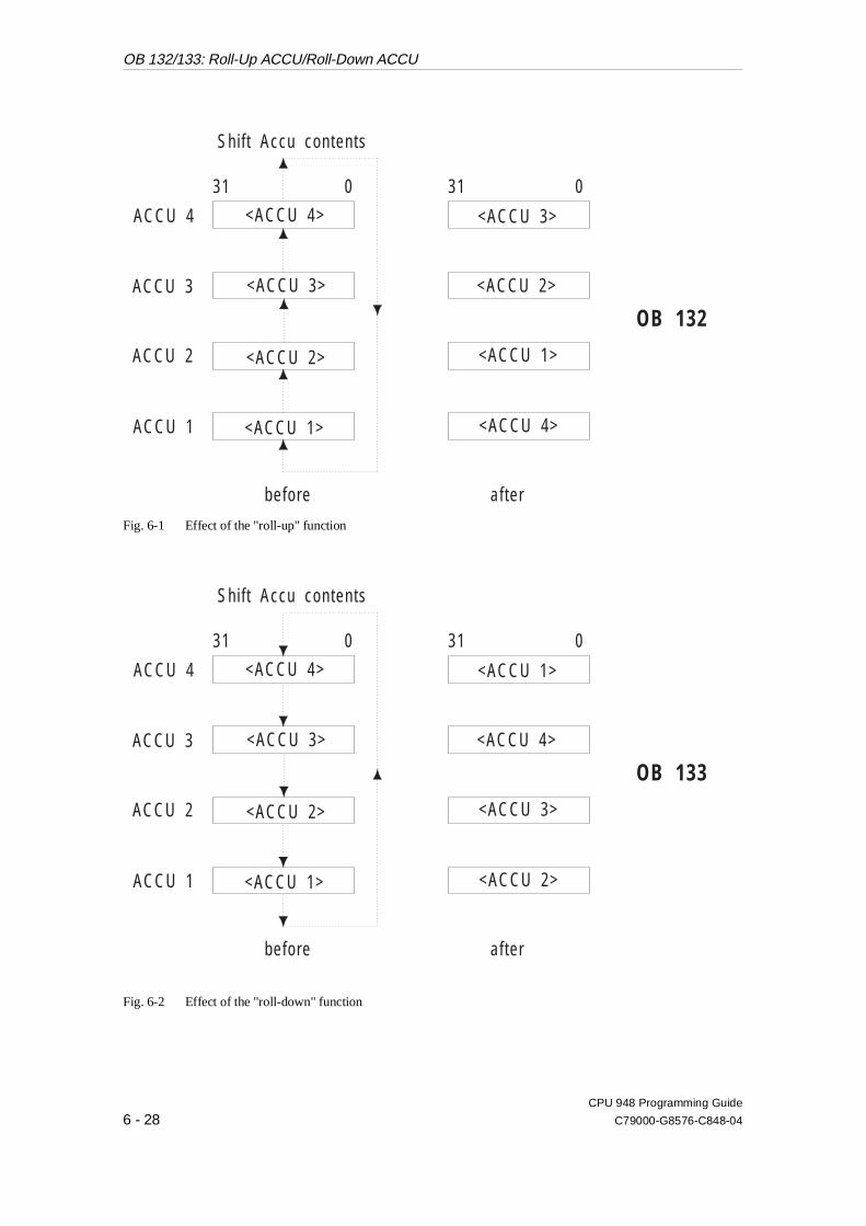
ACCU 4
ACCU 2
ACCU 3
ACCU 1
31 0 31 0
<ACCU 4>
<ACCU 2>
<ACCU 3>
<ACCU 1>
<ACCU 4>
<ACCU 2>
<ACCU 3>
<ACCU 1>
OB 132
before after
Shi f t Accu contents
Fig. 6-1 Effect of the "roll-up" function
ACCU 4
ACCU 2
ACCU 3
ACCU 1
31 0 31 0
<ACCU 2>
<ACCU 4>
<ACCU 1>
<ACCU 3>
<ACCU 4>
<ACCU 2>
<ACCU 3>
<ACCU 1>
OB 133
before after
Shi f t Accu contents
Fig. 6-2 Effect of the "roll-down" function
OB 132/133: Roll-Up ACCU/Roll-Down ACCU
CPU 948 Programming Guide
6 - 28 C79000-G8576-C848-04
6.10 OB 141: "Disable Single Cyclic Timed Interrupts" On/Off
Using OB 141, you can prevent certain cyclic timed interrupt OBs (timedinterrupts at fixed intervals ) from being called at one or moreconsecutive block or operation boundaries. For example, you can preventan OB 10 (period 1) and an OB 11 (period 2) from being called in aparticular program section that must not be interrupted. On the otherhand, all remaining programmed timed interrupts are processed as usual.
Function OB 141 affects the reaction to cyclic timed interrupts.
"Disable single cyclic timed interrupts" on means that none of thespecified cyclic timed interrupts are registered from this point onwardsand the interrupts that were already registered (e.g. those waiting for ablock boundary) are deleted. If a timed interrupt OB (for processing atimed interrupt with a fixed interval) has already been started, it isprocessed completely.
"Disable single cyclic timed interrupts" off means that all cyclic timedinterrupts are registered again and are processed at the next block oroperation boundary (depending on the setting in DX 0).
Parameters 1. Control word
OB 141 records the timed interrupts to be disabled in a system-internalcontrol word:
Bit no. 15 0
C o n t r o l w o r d
The bits of the control word have the following significance:
Bit no. Interrupt
0 to 2 Reserved, these bits must be ’0’
3 = ’1’4 = ’1’5 = ’1’6 = ’1’7 = ’1’8 = ’1’9 = ’1’10 = ’1’11 = ’1’
Cyclic timed interrupts with fixed interval:period 1 (OB 10)period 2 (OB 11)period 3 (OB 12)period 4 (OB 13)period 5 (OB 14)period 6 (OB 15)period 7 (OB 16)period 8 (OB 17)period 9 (OB 18)
12 to 15 Reserved; these bits must be ’0’
As long as a bit is set to ’1’ the corresponding interrupt is disabled.
OB 141: "Disable Single Cyclic Timed Interrupts" On/Off
CPU 948 Programming Guide
C79000-G8576-C848-04 6 - 29

2. ACCUs
2a) ACCU-2-L
Function no.,Permitted values: 1, 2 or 3 where:
1: The contents of ACCU 1 are loaded in thecontrol word.
2: All the bits marked ’1’ in the mask in ACCU 1 are set to ’1’ in the control word.The new control word is loaded in ACCU 1
3: All the bits marked ’1’ in the mask in ACCU 1 are set to ’0’ in the control word.The new control word is loaded in ACCU 1
2b) ACCU 1
New control word or mask depending on the required function.
Result After correct and error-free processing the system program sets theRLO to ’0’.Calling OB 141 has the following results:
Funct. no.in ACCU-2-L
Contents of ACCU 1
before after
1
2
3
control word
mask
mask
control word
newcontrol word
newcontrol word
OB 141: "Disable Single Cyclic Timed Interrupts" On/Off
CPU 948 Programming Guide
6 - 30 C79000-G8576-C848-04

Possible errors If an error occurs, the system program sets the RLO to ’1’.The errors listed in the following table can occur. If an error occurs,the system program enters the error ID listed below in ACCU-1-L.
ID Meaning
8D01H8D02H
illegal function no. in ACCU-2-L 1)
one of the reserved bits in ACCU 1 is ’1’ 1)
1) the incorrect value is located in ACCU-2-L
Scan control word •• The status of the control word can be scanned with the followingprogram sequence:
1. load function no. ’2’ or ’3’ in ACCU-2-L,
2. load value ’0’ in ACCU 1,
3. call OB 141,
4. read out ACCU 1.
Table 6-9 Error IDs of OB 141 in ACCU-1-L
OB 141: "Disable Single Cyclic Timed Interrupts" On/Off
CPU 948 Programming Guide
C79000-G8576-C848-04 6 - 31

6.11 OB 142: "Delay All Interrupts" On/Off
A STEP 5 program can be interrupted at block or operation boundariesby programs with a higher priority. The process interrupts and alltimed interrupts belong to these higher priority program executionlevels. The runtime of the interrupted program is extended by theruntime of the nested programs. Using OB 142, you can prevent thenesting of higher priority program execution levels at one or moreconsecutive block or operation boundaries (depending on the settingin DX 0).
Function OB 142 affects the servicing of interrupts:
"Delay interrupts" on means that all interrupts occurring are registeredand pending interrupts remain registered. The registered interrupts are,however, initially not serviced. The operation or block boundaries forservicing interrupts are temporarily made ineffective. If an OB for processinterrupt servicing or an OB for timed interrupt servicing has alreadystarted, this is processed completely.
"Delay interrupts" off means that all registered interrupts are processed atthe next block or operation boundary.
NoteThe time in which the interrupts are delayed must be shorter thanthree times the value of the shortest timed interrupt period. Ifthis is not the case, a collision of timed interrupts occurs.
Parameters 1. Control word
OB 142 enters the interrupts to be delayed in a system-internal controlword, as follows:
Bit no. 15 0
C o n t r o l w o r d
OB 142: "Delay All Interrupts" On/Off
CPU 948 Programming Guide
6 - 32 C79000-G8576-C848-04
The bits in the control word have the following meaning:
Bit no. Type of interrupt
0 = ’1’ Cyclic timed interrupts, fixed period
1 = ’1’ Clock-controlled interrupt
2 = ’1’ Process interrupts
3 = ’1’ Delayed interrupt
4 to 15 Reserved: these bits must be ’0’
As long as a bit is set to ’1’, the corresponding interrupt is disabled.
2. ACCUs
2a) ACCU-2-L
Function no.,Permitted values: 1, 2 or 3 where:
1: The contents of ACCU 1 are loaded in thecontrol word.
2: All the bits marked ’1’ in the mask in ACCU 1 are set to ’1’ in the control word.The new control word is loaded in ACCU 1
3: All the bits marked ’1’ in the mask in ACCU 1 are set to ’0’ in the control word.The new control word is loaded in ACCU 1
2b) ACCU 1
New control word or mask depending on the required function.
OB 142: "Delay All Interrupts" On/Off
CPU 948 Programming Guide
C79000-G8576-C848-04 6 - 33
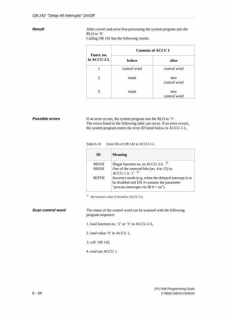
Result After correct and error-free processing the system program sets theRLO to ’0’.Calling OB 142 has the following results:
Funct. no.in ACCU-2-L
Contents of ACCU 1
before after
1
2
3
control word
mask
mask
control word
newcontrol word
newcontrol word
Possible errors If an error occurs, the system program sets the RLO to ’1’.The errors listed in the following table can occur. If an error occurs,the system program enters the error ID listed below in ACCU-1-L.
ID Meaning
8E01H8E02H
8EFFH
Illegal function no. in ACCU-2-L 1)
One of the reserved bits (no. 4 to 15) inACCU 1 is ’1’ 1)
Incorrect mode (e.g. when the delayed interrupt is tobe disabled and DX 0 contains the parameter"process interrupts via IB 0 = on")
1) the incorrect value is located in ACCU-2-L
Scan control word The status of the control word can be scanned with the followingprogram sequence:
1. load function no. ’2’ or ’3’ in ACCU-2-L,
2. load value ’0’ in ACCU 1,
3. call OB 142,
4. read out ACCU 1.
Table 6-10 Error IDs of OB 142 in ACCU-1-L
OB 142: "Delay All Interrupts" On/Off
CPU 948 Programming Guide
6 - 34 C79000-G8576-C848-04
6.12 OB 143: "Delay Single Cyclic Timed Interrupts" On/Off
Using OB 143, you can prevent certain cyclic timed interrupt OBs(timed interrupt OBs with a fixed period) from being called at one ormore consecutive block or operation boundaries. For example, youcan select a program section which cannot be interrupted by an OB 10(period 1) and an OB 11 (period 2). On the other hand, all theremaining programmed timed interrupts are processed as usual.
Function OB 143 affects the processing of cyclic timed interrupts:"Delay single cyclic timed interrupts" on means that all interrupts areregistered and pending timed interrupts remain registered. The timedinterrupts specified in the control word are, however, not processedimmediately. Temporarily, all the operation and block boundaries forprocessing these timed interrupts are made ineffective. If a timed interruptOB (for processing a timed interrupt with fixed period) has alreadystarted, it is processed completely.
"Delay single cyclic timed interrupts" off means that all registeredinterrupts are serviced at the next block or operation boundary (dependingon the setting in DX 0).
Parameters 1. Control word
OB 143 enters the timed interrupts to be delayed in a system-internalcontrol word:
Bit no. 15 0
C o n t r o l w o r d
The bits in the control word have the following meaning:
Bit no. Interrupt
0 to 2 Reserved, these bits must be ’0’
3 = ’1’4 = ’1’5 = ’1’6 = ’1’7 = ’1’8 = ’1’9 = ’1’
Cyclic timed interrupts with fixed periodperiod 1 (OB 10)period 2 (OB 11)period 3 (OB 12)period 4 (OB 13)period 5 (OB 14)period 6 (OB 15)period 7 (OB 16)
10 = ’1’11 = ’1’
period 8 (OB 17)period 9 (OB 18)
12 to 15 Reserved, these bits must be ’0’
As long as a bit is set to ’1’, the corresponding interrupt is disabled.
OB 143: "Delay Single Cyclic Timed Interrupts" On/Off
CPU 948 Programming Guide
C79000-G8576-C848-04 6 - 35
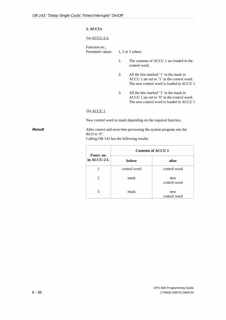
2. ACCUs
2a) ACCU-2-L
Function no.,Permitted values: 1, 2 or 3 where:
1: The contents of ACCU 1 are loaded in thecontrol word.
2: All the bits marked ’1’ in the mask in ACCU 1 are set to ’1’ in the control word.The new control word is loaded in ACCU 1
3: All the bits marked ’1’ in the mask in ACCU 1 are set to ’0’ in the control word.The new control word is loaded in ACCU 1
2b) ACCU 1
New control word or mask depending on the required function.
Result After correct and error-free processing the system program sets theRLO to ’0’.Calling OB 143 has the following results:
Funct. no.in ACCU-2-L
Contents of ACCU 1
before after
1
2
3
control word
mask
mask
control word
newcontrol word
newcontrol word
OB 143: "Delay Single Cyclic Timed Interrupts" On/Off
CPU 948 Programming Guide
6 - 36 C79000-G8576-C848-04
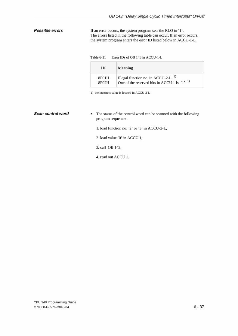
Possible errors If an error occurs, the system program sets the RLO to ’1’.The errors listed in the following table can occur. If an error occurs,the system program enters the error ID listed below in ACCU-1-L.
ID Meaning
8F01H8F02H
Illegal function no. in ACCU-2-L 1)
One of the reserved bits in ACCU 1 is ’1’ 1)
1) the incorrect value is located in ACCU-2-L
Scan control word •• The status of the control word can be scanned with the followingprogram sequence:
1. load function no. ’2’ or ’3’ in ACCU-2-L,
2. load value ’0’ in ACCU 1,
3. call OB 143,
4. read out ACCU 1.
Table 6-11 Error IDs of OB 143 in ACCU-1-L
OB 143: "Delay Single Cyclic Timed Interrupts" On/Off
CPU 948 Programming Guide
C79000-G8576-C848-04 6 - 37

6.13 OB 150: Set/Read System Time
Features of the system time
•• The system time is backed up by the battery in the PLC rack. If thetime is set, it therefore remains correct even following a powerfailure.
•• The resolution is 10 ms for reading and 1 s for setting.
•• Leap years are taken into account.
•• Hours can be represented either using the 24 hour clock or the 12hour clock "am" and "pm".
•• The weekday is specified.
•• Input and output is BCD coded.
Function Using OB 150, you can set or read out the date and time of the CPU 948in your user program. The date and time are known as the "system time".
NoteThe system time is started (initially with a default value) after theCPU is plugged in.
Parameters 1. Data field for the time parameters
When setting the system time, OB 150 reads in the values to be setfrom a data field, when reading the time, OB 150 transfers the currenttime to the data field. You can set up this data field in a data block orin one of the two flag areas (F or S flags).
The data field consists of four words.
1a) Format of the data field for setting the system time.
Bit no. 15 12 11 8 7 4 3 0
word 1 Seconds 0
word 2 Format Hours Minutes
word 3 Day of month Weekday 0
word 4 Year Month
OB 150: Set/Read System Time
CPU 948 Programming Guide
6 - 38 C79000-G8576-C848-04

1b) Format of the data field when reading the system time
Bit no. 15 12 11 8 7 4 3 0
word 1 Seconds 1/100 seconds
word 2 Format Hours Minutes
word 3 Day of month Weekday 0
word 4 Year Month
The time parameters have the following meaning, range of values andrepresentation:
Parameter Permitted range of values Value in
Seconds1/100 secondsMinutesHours
WeekdayDay of month1)
MonthYear
0 to 590 to 99 (with "set system time" = 00 to 590 to 23 or 1 to 12, depending on the"format"0 to 6 for Mon to Sun1 to 31 1 to 120 to 99
BCD format
Format Format for the hour field with thefollowing meaning:Bit 15 = 0: 12 hour format
("am" or "pm"selected in bit 14)
Bit 15 = 1: 24 hour format(bit 14 = 0)
Bit 14 = 0: "am"Bit 14 = 1: "pm"
–
1) After OB 150 is called, the specified value is checked logically for the correct datataking into account leap years.
Data field in the flag area If you set up the data field in a flag area, you must take into account thefollowing assignment of the data field words to the flag bytes. ’x’ is theparameter "number of 1st data field word" which must be written toACCU-1-L when OB 150 is called:
Bit no. 15 8 7 0
Data field word 1 Flag byte x Flag byte x+1
Data field word 2 Flag byte x+2 Flag byte x+3
Data field word 3 Flag byte x+4 Flag byte x+5
Data field word 4 Flag byte x+6 Flag byte x+7
OB 150: Set/Read System Time
CPU 948 Programming Guide
C79000-G8576-C848-04 6 - 39

2. ACCUs
2a) ACCU-2-L
ACCU-2-L contains information about the required function and thedata field used. It must have the following structure:
Bit no. 15 12 11 8 7 4 3 0
Function no. Address area type Data block no.
Parameters in ACCU-2-L
Function no.,Permitted values: 1 = set system time
2 = read system time
Address area type,Permitted values: 1 = DB data block
2 = DX data block3 = F flag area4 = S flag area
Data block no.,Permitted values: 3 to 255 (only with address area type ’1’ or ’2’;
with address area type ’3’ or ’4’ irrelevant)
2b) ACCU-1-L
Number of the 1st data field wordPermitted values (depending on the address area type):
DB, DX: 0 to 2039F flags: 0 to 248
(= no. of flag byte ’x ’)S flags 0 to 4088
(= no. of flag byte ’x ’)
Result After correct processing of OB 150, the RLO, the condition code bitsOR, ERAB and OS = 0.
Possible errors The errors listed in the following table may occur. If an error occurs,the system program sets the RLO to ’1’ and stores the error IDs listedin the table in ACCU 1.
OB 150: Set/Read System Time
CPU 948 Programming Guide
6 - 40 C79000-G8576-C848-04
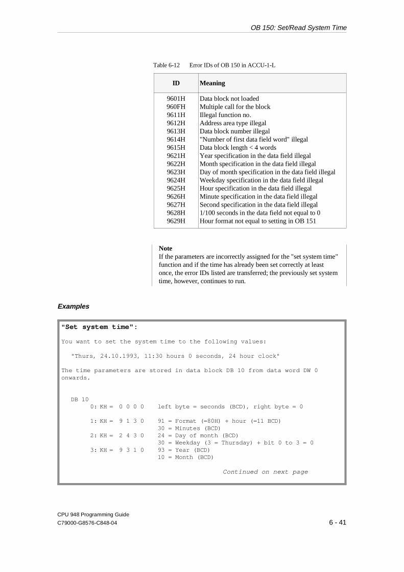
ID Meaning
9601H960FH9611H9612H9613H9614H9615H9621H9622H9623H9624H9625H9626H9627H9628H9629H
Data block not loadedMultiple call for the blockIllegal function no.Address area type illegalData block number illegal"Number of first data field word" illegalData block length < 4 wordsYear specification in the data field illegalMonth specification in the data field illegalDay of month specification in the data field illegalWeekday specification in the data field illegalHour specification in the data field illegalMinute specification in the data field illegalSecond specification in the data field illegal1/100 seconds in the data field not equal to 0Hour format not equal to setting in OB 151
NoteIf the parameters are incorrectly assigned for the "set system time"function and if the time has already been set correctly at leastonce, the error IDs listed are transferred; the previously set systemtime, however, continues to run.
Examples
Table 6-12 Error IDs of OB 150 in ACCU-1-L
" Set system time":
You want to set the system time to the following values:
"Thurs, 24.10.1993, 11:30 hours 0 seconds, 24 hour clock"
The time parameters are stored in data block DB 10 from data word DW 0onwards.
DB 100: KH = 0 0 0 0 left byte = seconds (BCD), right byte = 0
1: KH = 9 1 3 0 91 = Format (=80H) + hour (=11 BCD) 30 = Minutes (BCD)
2: KH = 2 4 3 0 24 = Day of month (BCD)30 = Weekday (3 = Thursday) + bit 0 to 3 = 0
3: KH = 9 3 1 0 93 = Year (BCD)10 = Month (BCD)
Continued on next page
OB 150: Set/Read System Time
CPU 948 Programming Guide
C79000-G8576-C848-04 6 - 41
"Read out system time":
You want the current system time to be written to data block DB 10 from dataword DW 4 onwards. You must therefore call OB 150 with the followingparameters:
:::L KH 2 1 0 A Values for ACCU-2-L:: DB no. = 10: Address area type = 1 for "data field in DB": Function no. = 2 for "read":L KF +4 ACCU-1-L:: No. of 1st data field word = 4:JU OB 150 Call OB 150:C DB 10 Open DB 10: Evaluate DB 10
After OB 150 is called, the current system time is written to data block DB10 in the following form ("Thurs, 24.10.93, 11:30 hours 20 seconds, 13/100of a second, 24 hour clock"):
DW 4: KH = 2 0 1 3 Seconds = 20 (BCD)1/100 seconds = 13 (BCD)
DW 5: KH = 9 1 3 0 Format = 24 hour (bit 15 = 1, bit 14 = 0), Hour = 11(BCD), minutes = 30 (BCD)
DW 6: KH = 2 4 3 0 Day of month = 24 (BCD)Weekday = 3 = Thursday
DW 7: KH = 9 3 1 0 Year = 93 (BCD)Month = 10 (BCD)
" Set system time" (continued)
STEP 5 operations in OB 1 for calling OB 150:
: ::L KH 1 1 0 A Values for ACCU-2-L:: DB no. = 10: Address area type = 1 for "data field in DB": Function no. = 1 for "set":L KF +0 ACCU-1-L: : No. of 1st data field word = 0:JU OB 150 Call OB 150:
OB 150: Set/Read System Time
CPU 948 Programming Guide
6 - 42 C79000-G8576-C848-04

6.14 OB 151: Set/Read Time for Clock-Controlled Interrupt
Function By calling OB 151 you can do the following:
•• cause the CPU 948 to activate the clock-controlled interrupt ("timedjob" - OB 9, refer to Section 4.5.3) at a selected time:
- every minute- every hour- every day- every week - every month- every year- once,
•• read out the current status of a timed job,
•• cancel a previously generated timed job.
OB 151 can be called in the START-UP and RUN modes. A generatedclock-controlled interrupt is retained when a WARM RESTART(automatic or manual) is carried out. A COLD RESTART deletes anexisting timed job.
If you generate a new timed job, an existing timed job is automaticallycancelled. This means that only one clock-controlled interrupt can beactive.
Parameters 1. Data field for job parameters
When generating or cancelling a timed job, OB 151 takes therequired job parameters from a data field. When reading out thecurrent status of the job management, OB 151 transfers the current jobparameters to a data field.
You can set up this data field in a data block or in one of the two flagareas (F or S flags).
The data field consists of four words and has the following formatwhen generating and reading out a timed job:
Bit no. 15 12 11 8 7 4 3 0
Word 1 Seconds 0
Word 2 Format Hours Minutes
Word 3 Day of month Weekday Job type
Word 4 Year Month
OB 151: Set/Read Time for Clock-Controlled Interrupt
CPU 948 Programming Guide
C79000-G8576-C848-04 6 - 43
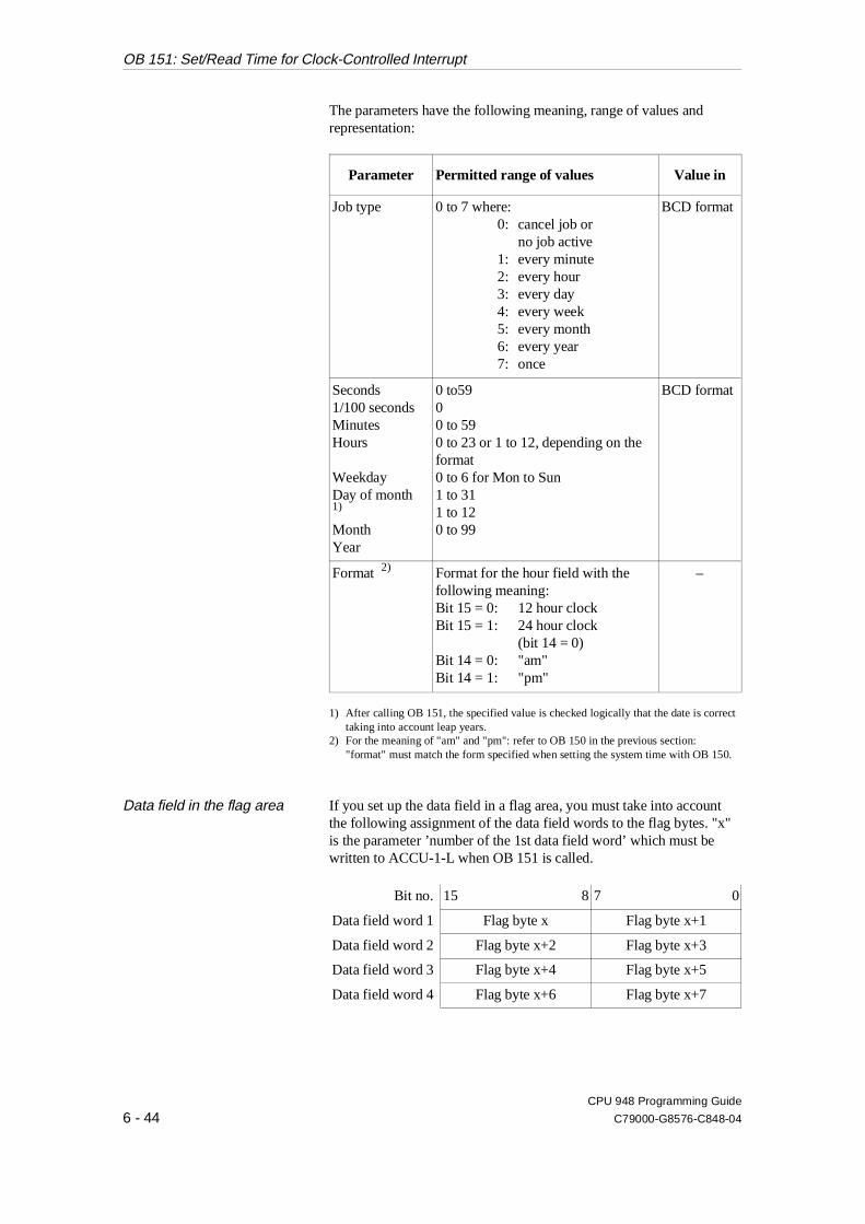
The parameters have the following meaning, range of values andrepresentation:
Parameter Permitted range of values Value in
Job type 0 to 7 where:0: cancel job or
no job active1: every minute2: every hour3: every day4: every week5: every month6: every year7: once
BCD format
Seconds1/100 secondsMinutesHours
WeekdayDay of month1)
MonthYear
0 to590 0 to 590 to 23 or 1 to 12, depending on theformat0 to 6 for Mon to Sun1 to 31 1 to 120 to 99
BCD format
Format 2) Format for the hour field with thefollowing meaning:Bit 15 = 0: 12 hour clockBit 15 = 1: 24 hour clock
(bit 14 = 0)Bit 14 = 0: "am"Bit 14 = 1: "pm"
–
1) After calling OB 151, the specified value is checked logically that the date is correcttaking into account leap years.
2) For the meaning of "am" and "pm": refer to OB 150 in the previous section:"format" must match the form specified when setting the system time with OB 150.
Data field in the flag area If you set up the data field in a flag area, you must take into accountthe following assignment of the data field words to the flag bytes. "x"is the parameter ’number of the 1st data field word’ which must bewritten to ACCU-1-L when OB 151 is called.
Bit no. 15 8 7 0
Data field word 1 Flag byte x Flag byte x+1
Data field word 2 Flag byte x+2 Flag byte x+3
Data field word 3 Flag byte x+4 Flag byte x+5
Data field word 4 Flag byte x+6 Flag byte x+7
OB 151: Set/Read Time for Clock-Controlled Interrupt
CPU 948 Programming Guide
6 - 44 C79000-G8576-C848-04
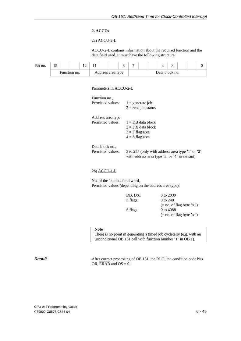
2. ACCUs
2a) ACCU-2-L
ACCU-2-L contains information about the required function and thedata field used. It must have the following structure:
Bit no. 15 12 11 8 7 4 3 0
Function no. Address area type Data block no.
Parameters in ACCU-2-L
Function no.,Permitted values: 1 = generate job
2 = read job status
Address area type,Permitted values: 1 = DB data block
2 = DX data block3 = F flag area4 = S flag area
Data block no.,Permitted values: 3 to 255 (only with address area type ’1’ or ’2’;
with address area type ’3’ or ’4’ irrelevant)
2b) ACCU-1-L
No. of the 1st data field word,Permitted values (depending on the address area type):
DB, DX: 0 to 2039F flags: 0 to 248
(= no. of flag byte ’x ’)S flags 0 to 4088
(= no. of flag byte ’x ’)
NoteThere is no point in generating a timed job cyclically (e.g. with anunconditional OB 151 call with function number ’1’ in OB 1).
Result After correct processing of OB 151, the RLO, the condition code bitsOR, ERAB and OS = 0.
OB 151: Set/Read Time for Clock-Controlled Interrupt
CPU 948 Programming Guide
C79000-G8576-C848-04 6 - 45
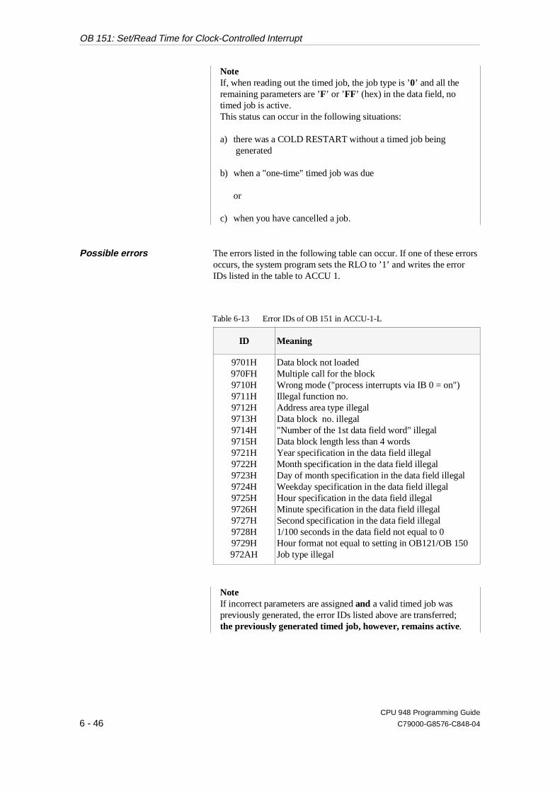
NoteIf, when reading out the timed job, the job type is ’0’ and all theremaining parameters are ’F’ or ’FF’ (hex) in the data field, notimed job is active.This status can occur in the following situations:
a) there was a COLD RESTART without a timed job being generated
b) when a "one-time" timed job was due
or
c) when you have cancelled a job.
Possible errors The errors listed in the following table can occur. If one of these errorsoccurs, the system program sets the RLO to ’1’ and writes the errorIDs listed in the table to ACCU 1.
ID Meaning
9701H970FH9710H9711H9712H9713H9714H9715H9721H9722H9723H9724H9725H9726H9727H9728H9729H972AH
Data block not loadedMultiple call for the blockWrong mode ("process interrupts via IB 0 = on")Illegal function no.Address area type illegalData block no. illegal"Number of the 1st data field word" illegalData block length less than 4 wordsYear specification in the data field illegal Month specification in the data field illegalDay of month specification in the data field illegalWeekday specification in the data field illegalHour specification in the data field illegalMinute specification in the data field illegalSecond specification in the data field illegal1/100 seconds in the data field not equal to 0Hour format not equal to setting in OB121/OB 150Job type illegal
NoteIf incorrect parameters are assigned and a valid timed job waspreviously generated, the error IDs listed above are transferred;the previously generated timed job, however, remains active.
Table 6-13 Error IDs of OB 151 in ACCU-1-L
OB 151: Set/Read Time for Clock-Controlled Interrupt
CPU 948 Programming Guide
6 - 46 C79000-G8576-C848-04

Points to note with the timeparameters
Regardless of when a clock-controlled interrupt (timed job) is to betriggered, the individual time parameters must be specified in certaincombinations. Depending on the selected time for the clock-controlledinterrupt, certain parameters must be specified, while others are notevaluated by the system program.
The following table shows which time parameters must be specifiedfor which timed job (XXX = must be specified, --- = irrelevant).
Interval Seconds Minu-tes
Hours Week-day
Day ofmonth
Month Year
every minuteevery hourevery dayevery weekevery monthevery yearonce
XXXXXXXXXXXXXXXXXXXXX
---XXXXXXXXXXXXXXXXXX
------
XXXXXXXXXXXXXXX
---------
XXX---------
------------
XXXXXXXXX
---------------
XXXXXX
------------------
XXX
When reading out the time parameters, the irrelevant parameters areassigned the value FFH.
Special situations •• If the "29th of February" is selected with the job type "every year"(= 6), this means that OB 9 is only called every leap year.
•• If the value "29", "30" or "31" is selected with the job type "everymonth" (= 5), OB 9 is only called in the months which have thesedates.
Table 6-14 Assignment of "timed job - time parameters"
OB 151: Set/Read Time for Clock-Controlled Interrupt
CPU 948 Programming Guide
C79000-G8576-C848-04 6 - 47
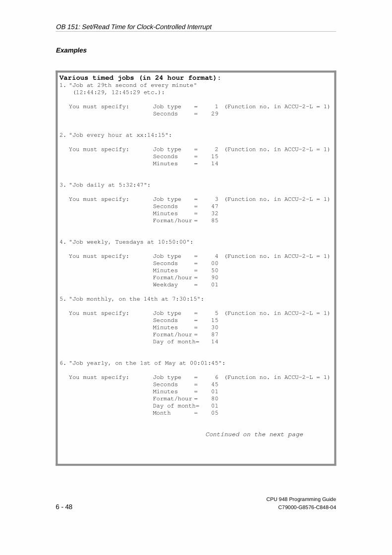
Examples
Various timed jobs (in 24 hour format):1. "Job at 29th second of every minute"
(12:44:29, 12:45:29 etc.):
You must specify: Job type = 1 (Function no. in ACCU-2-L = 1)Seconds = 29
2. "Job every hour at xx:14:15":
You must specify: Job type = 2 (Function no. in ACCU-2-L = 1)Seconds = 15Minutes = 14
3. "Job daily at 5:32:47":
You must specify: Job type = 3 (Function no. in ACCU-2-L = 1)Seconds = 47Minutes = 32Format/hour = 85
4. "Job weekly, Tuesdays at 10:50:00":
You must specify: Job type = 4 (Function no. in ACCU-2-L = 1)Seconds = 00Minutes = 50Format/hour = 90Weekday = 01
5. "Job monthly, on the 14th at 7:30:15":
You must specify: Job type = 5 (Function no. in ACCU-2-L = 1)Seconds = 15Minutes = 30Format/hour = 87Day of month= 14
6. "Job yearly, on the 1st of May at 00:01:45":
You must specify: Job type = 6 (Function no. in ACCU-2-L = 1)Seconds = 45Minutes = 01Format/hour = 80Day of month= 01Month = 05
Continued on the next page
OB 151: Set/Read Time for Clock-Controlled Interrupt
CPU 948 Programming Guide
6 - 48 C79000-G8576-C848-04

Various timed jobs (in 24 hour format), continued :7. "Job once on the 31.12.1999 at 23:55:00":
You must specify: Job type = 7 (Function no. in ACCU-2-L = 1)Seconds = 00Minutes = 55Format/hour = A3Day of month= 31Month = 12Year = 99
8. "Cancel job":
You must specify: Job type = 0 (Function no. in ACCU-2-L = 1)
9. "Read out time job":
You must specify: Function no. in ACCU-2-L = 2
If no job is active, you obtain the following result in the data field:
Data field word 0: FFFF HData field word 1: FFFF HData field word 2: FFF0 HData field word 3: FFFF H
OB 151: Set/Read Time for Clock-Controlled Interrupt
CPU 948 Programming Guide
C79000-G8576-C848-04 6 - 49
6.15 OB 153: Set/Read Time for Delayed Interrupt
Using OB 153, you can transfer so-called "delay jobs" to the systemprogram. After a specified delay time "a delayed interrupt" is thenprocessed (refer to OB 6, Section 4.5.3).
Function By calling OB 153, you can do the following:
•• define and start a delay time,
•• stop an activated delay time (cancel delay job),
•• read how long the delay time still has to run.
A delay job can be activated in the START UP and RUN modes.
Life of a delay job The delayed interrupt triggered by a delay job is only activated by thesystem program in the RUN mode (OB 6 call).Jobs which become due in a mode other than RUN are discarded bythe system program without any message.A currently active (but not yet due) job is also discarded if the CPUchanges to the STOP mode or if the power is switched off.
Parameters ACCUs
a) ACCU-2-L
ACCU-2-L only needs to be supplied with the function number ’1’("define delay time") when OB 153 is called, as follows:
Delay time in milliseconds (max. 65535)
Permitted values: 0001H to FFFFH
b) ACCU-1-L
Function no.
Permitted values: 1 = define and start delay time2 = stop delay time (= cancel job)3 = read remaining delay time
OB 153: Set/Read Time for Delayed Interrupt
CPU 948 Programming Guide
6 - 50 C79000-G8576-C848-04
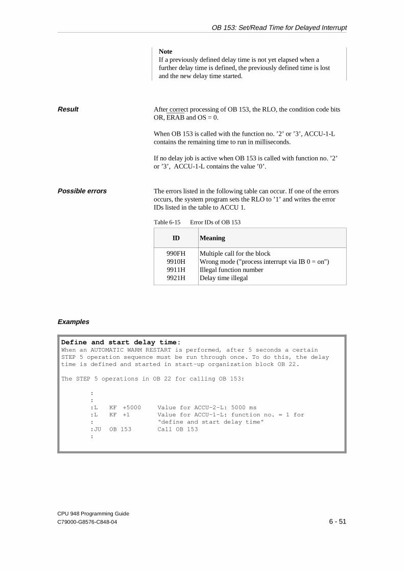
NoteIf a previously defined delay time is not yet elapsed when afurther delay time is defined, the previously defined time is lostand the new delay time started.
Result After correct processing of OB 153, the RLO, the condition code bitsOR, ERAB and OS = 0.
When OB 153 is called with the function no. ’2’ or ’3’, ACCU-1-Lcontains the remaining time to run in milliseconds.
If no delay job is active when OB 153 is called with function no. ’2’or ’3’, ACCU-1-L contains the value ’0’.
Possible errors The errors listed in the following table can occur. If one of the errorsoccurs, the system program sets the RLO to ’1’ and writes the errorIDs listed in the table to ACCU 1.
ID Meaning
990FH9910H9911H9921H
Multiple call for the blockWrong mode ("process interrupt via IB 0 = on")Illegal function numberDelay time illegal
Examples
Table 6-15 Error IDs of OB 153
Define and start delay time:When an AUTOMATIC WARM RESTART is performed, after 5 seconds a certainSTEP 5 operation sequence must be run through once. To do this, the delaytime is defined and started in start-up organization block OB 22.
The STEP 5 operations in OB 22 for calling OB 153:
: ::L KF +5000 Value for ACCU-2-L: 5000 ms:L KF +1 Value for ACCU-1-L: function no. = 1 for: "define and start delay time":JU OB 153 Call OB 153:
OB 153: Set/Read Time for Delayed Interrupt
CPU 948 Programming Guide
C79000-G8576-C848-04 6 - 51

Stop delay time (cancel job)STEP 5 operations for calling OB 153:
: ::L KF +2 Value for ACCU-1-L: function no. = 2 for: "stop delay time":JU OB 153 Call OB 153::
Read out remaining time of a delay job:STEP 5 operations for calling OB 153:
: ::L KF +3 Value for ACCU-1-L: function no. = 3 for: "read out remaining time":JU OB 153 Call OB 153:: ACCU-1-L contains the time the delay job still: has to run.:
OB 153: Set/Read Time for Delayed Interrupt
CPU 948 Programming Guide
6 - 52 C79000-G8576-C848-04
6.16 OB 180: Variable Data Block Access
Using OB 180 You can use OB 180 when working with data blocks that are longerthan 261 words (incl. 5 words header).Using OB 180, you can shift an "access window" of 256 data words insteps of 16 words over a data block (at paragraph addresses). CallOB 180 each time you want to shift the access window further.
In contrast to the CPU 928B, you cannot shift the access windowcontinuously but only in steps that are multiples of 16.
Function When you use OB 180, the start address of the current data block isshifted towards the end of the block by the specified value. This takesinto account that the length of DB still available is reduced (DBA andDBL registers are loaded in keeping with the shift, see Sections 8.3and 9.2.1).
NoteBefore calling OB 180, a data block (DB or DX) with an adequatelength must already be open.
Parameters ACCU-1-L
Shift number S: Number of data words, by which the data block startaddress will be shifted.
Permitted values: 0 ≤ V < DBL, S = n * 16 (16, 32, 48 ...)
Result After you have called OB 180 succesfully:
•• the relative address of DW 0 is shifted by the value contained inACCU-1-L (the DBA and DBL registers are updated accordingly),
•• the RLO is cleared (RLO = 0),
•• all other bit and word codes are cleared,
•• the content of ACCU-1-L = 0.
OB 180: Variable Data Block Access
CPU 948 Programming Guide
C79000-G8576-C848-04 6 - 53

Possible errors The errors listed in the following table can occur. If an error doesoccur, the system program sets the RLO to ’1’ and enters the error IDslisted in the table in ACCU 1. The other bit and word codes arecleared.The values of the DBA and DBL remain unchanged.
ID Meaning
B401HB410HB411H
No data block is openThe shift number S is not a multiple of 16a) The shift number is too high; the block end is exceeded by the new window position.b) The shift number is negative.
Setting the access windowback to the start value
Opening the data block again with the operations C DB or C DXreturns the access window to its original position.
Reaction to nesting If the access window is shifted by calling OB 180 in a logic block anda further logic block is then called, the position of the access windowremains where it is in the called logic block until OB 180 is calledagain (the DBA/DBL values do not change).
If, on the other hand, the access window is shifted in a called logicblock by calling OB 180, when program execution returns from thecalled block (block end operation), it is returned to the position ithad when the nested logic block was called.
Table 6-16 Error IDs of OB 180
OB 180: Variable Data Block Access
CPU 948 Programming Guide
6 - 54 C79000-G8576-C848-04

Example
You want the data block start address (DBA = 4152H in DB 17, length = 256DW) to be shifted by 32 data words relative to the end of the block.
:C DB 17 open DB 17:L KB 32 shift value as constant:JU OB 180 call OB 180: shift access window
After OB 180 has been called, the data word, for example, at address 41543H can no longer be addressed with DW 35 but only with DW 3 etc. (seeFig. 6-3).
Due to the change made at the same time in the DBL register, error monitoringis not affected: the operation T DW 223 is permitted, while T DW 224/L DW 224causes an error.
By calling OB 180 again, the DBA can be increased again (and the DBLreduced). The operation C DB 17 returns the block to its original settings(DBA = 4152H, length 256 DW).If DB 17 had a length of 256 data words for example, you could then nolonger access DW 256 and DW 257 using STEP 5 operations. By shifting theDBA resgister by 16, data words 256 and 257 can be addressed as "DW 240"and "DW 241".
Continued on next page
OB 180: Variable Data Block Access
CPU 948 Programming Guide
C79000-G8576-C848-04 6 - 55
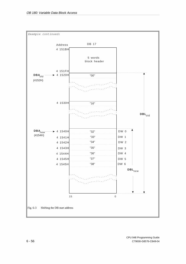
Example continued:
4 1520H
4 1530H
4 1540H
4 1541H
4 1542H
4 1543H
4 1544H
4 1545H
4 1545H
4 151FH
4 151BH
DW 0
DW 1
DW 2
DW 3
DW 4
DW 5
DW 6
Address DB 17
DBAnew
5 wordsblock header
DBAold
DBLold
DBLnew
15 0
"32"
"16"
"00"
"33"
"34"
"35"
"36"
"37"
"38"
(4152H)
(4154H)
Fig. 6-3 Shifting the DB start address
OB 180: Variable Data Block Access
CPU 948 Programming Guide
6 - 56 C79000-G8576-C848-04
6.17 OB 181: Test Data Blocks (DB/DX)
With the special function organization block OB 181, you can testdata blocks as follows:
•• whether or not a particular DB or DX data block exists,
•• the address at which the first data word of the data block is stored,
•• how many data words the data block contains.
Using OB 181 The function "test DB/DX" is useful before the operations TNB/TNW,G DB/GX DX and before calling special function organization blocksOB 182, OB 254 and OB 255.
Before transferring data words, for example, you can call OB 181 tocheck that the destination data block is valid and long enough for thetransfer.
Function OB 181 checks whether a specified data block exists and returns thecharacteristic parameters of a data block.
Parameters ACCU-1-L
a) ACCU-1-LL
Block number, Permitted values: 1 to 255
b) ACCU-1-LH
Block ID, Permitted values: 1 = DB
2 = DX
OB 181: Test Data Blocks (DB/DX)
CPU 948 Programming Guide
C79000-G8576-C848-04 6 - 57

Result If the function is executed without any error and if the block exists onthe CPU, the system program transfers the following values:
- ACCU-1-L: Address of the 1st data word (DW 0),20-bit address,
- ACCU-2-L: Length of the data block in words (withoutblock header)Example: ACCU-2-L contains the value’7’:
The data block consists of datawords DW 0 to DW 6,
- RLO: = 0.
Possible errors The errors listed in the table below can occur. If an error occurs, thesystem program sets the RLO to ’1’ and the following condition codebits as shown in the table. It also enters an error ID in ACCU-1-L.
RLO CC 1 CC 0 ACCU-1-L Meaning Scan
1 0 1 B501H Block does not exist JCJMJN
1 1 0 B502H Wrong block number JCJPJN
1 1 0 B503H Wrong block ID JCJPJN
Table 6-17 Error codes of OB 181 and their scans
OB 181: Test Data Blocks (DB/DX)
CPU 948 Programming Guide
6 - 58 C79000-G8576-C848-04
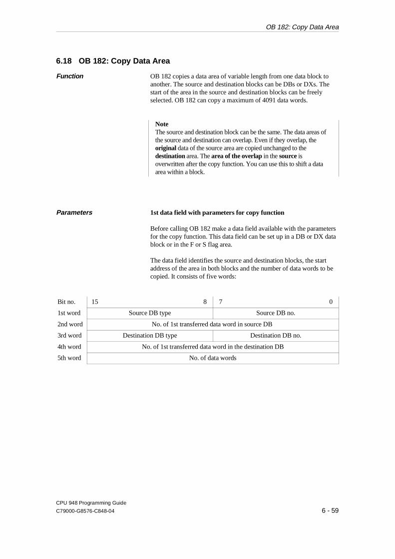
6.18 OB 182: Copy Data Area
Function OB 182 copies a data area of variable length from one data block toanother. The source and destination blocks can be DBs or DXs. Thestart of the area in the source and destination blocks can be freelyselected. OB 182 can copy a maximum of 4091 data words.
NoteThe source and destination block can be the same. The data areas ofthe source and destination can overlap. Even if they overlap, theoriginal data of the source area are copied unchanged to thedestination area. The area of the overlap in the source isoverwritten after the copy function. You can use this to shift a dataarea within a block.
Parameters 1st data field with parameters for copy function
Before calling OB 182 make a data field available with the parametersfor the copy function. This data field can be set up in a DB or DX datablock or in the F or S flag area.
The data field identifies the source and destination blocks, the startaddress of the area in both blocks and the number of data words to becopied. It consists of five words:
Bit no. 15 8 7 0
1st word Source DB type Source DB no.
2nd word No. of 1st transferred data word in source DB
3rd word Destination DB type Destination DB no.
4th word No. of 1st transferred data word in the destination DB
5th word No. of data words
OB 182: Copy Data Area
CPU 948 Programming Guide
C79000-G8576-C848-04 6 - 59
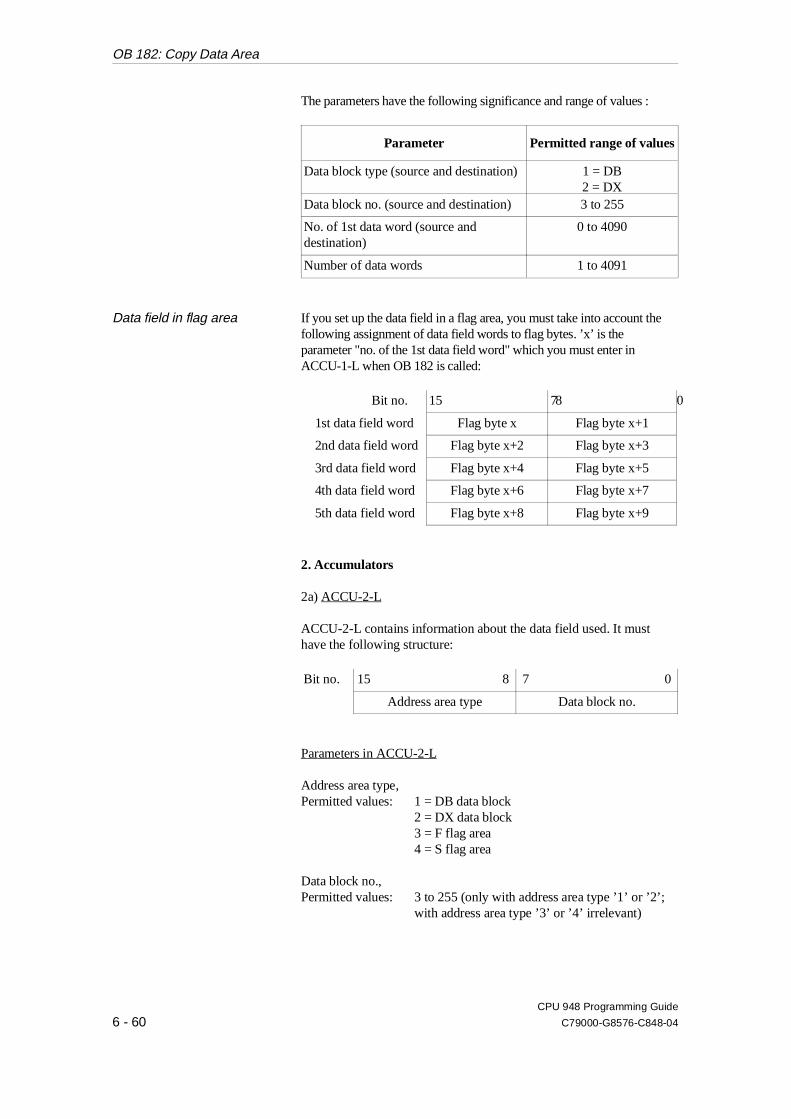
The parameters have the following significance and range of values :
Parameter Permitted range of values
Data block type (source and destination) 1 = DB2 = DX
Data block no. (source and destination) 3 to 255
No. of 1st data word (source anddestination)
0 to 4090
Number of data words 1 to 4091
Data field in flag area If you set up the data field in a flag area, you must take into account thefollowing assignment of data field words to flag bytes. ’x’ is theparameter "no. of the 1st data field word" which you must enter inACCU-1-L when OB 182 is called:
Bit no. 15 87 0
1st data field word Flag byte x Flag byte x+1
2nd data field word Flag byte x+2 Flag byte x+3
3rd data field word Flag byte x+4 Flag byte x+5
4th data field word Flag byte x+6 Flag byte x+7
5th data field word Flag byte x+8 Flag byte x+9
2. Accumulators
2a) ACCU-2-L
ACCU-2-L contains information about the data field used. It musthave the following structure:
Bit no. 15 8 7 0
Address area type Data block no.
Parameters in ACCU-2-L
Address area type,Permitted values: 1 = DB data block
2 = DX data block3 = F flag area4 = S flag area
Data block no.,Permitted values: 3 to 255 (only with address area type ’1’ or ’2’;
with address area type ’3’ or ’4’ irrelevant)
OB 182: Copy Data Area
CPU 948 Programming Guide
6 - 60 C79000-G8576-C848-04

2b) ACCU-1-L
Number of the 1st data field word,possible values (depending on theaddress area type:
DB, DX: 0 to 2038F flags: 0 to 246
(= No. of flag byte ’x ’)S flags 0 to 4086
(= No. of flag byte ’x ’)
Result After correctly processing OB 182: RLO, condition code bits OR,ERAB and OS = 0.
Possible errors If an error occurs, an error ID is entered in ACCU 1 (see table below).
ACCU-1-L Meaning
B601HB60FHB611HB612HB613HB621HB622HB623HB624H
B625H
B626HB627HB628H
B629HB62AH
B62BHB62CH
Data block not loadedMultiple block callIncorrect content in the data fieldAddress area type illegalData block no. illegal"Number of the 1st data field word" illegal"Source data block type" illegal"Source data block no." illegal"No. of the 1st data word to be transmitted in source DB" illegalLength of the source data block in the block header< 5 words"Destination data block type" illegal"Destination data block no." illegal"No. of 1st data word to written in destination DB" illegalLength of the destination block in block header < 5words"Number of data words to be transmitted" illegal(= 0 or > 4091)Source data block too shortDestination data block too short
Table 6-18 Error IDs of OB 182 in ACCU-1-L
OB 182: Copy Data Area
CPU 948 Programming Guide
C79000-G8576-C848-04 6 - 61
6.19 OB 202 to 205: Multiprocessor Communication
A detailed description of these special function organization blockscan be found in Chapter 10.
The special function organization blocks OB 200 and OB 202 toOB 205 allow data transfer between the individual CPUs using thecoordinator COR C in multiprocessor operation.
•• OB 200: initialize
This special function organization block sets up the memory in theCOR C coordinator in which the blocks of data to be transferred arebuffered.
•• OB 202: send
This function transfers a block of data to the buffer of the COR Cand specifies how many blocks of data can still be sent.
•• OB 203: send test
The special function OB 203 checks the number of free memoryfields in the buffer of the COR C.
•• OB 204: receive
This function accepts a block of data from the COR C buffer andindicates how many blocks of data can still be received.
•• OB 205: receive test
The special function organization block OB 205 checks the numberof occupied memory fields in the COR C buffer.
OB 202 to 205: Multiprocessor Communication
CPU 948 Programming Guide
6 - 62 C79000-G8576-C848-04
6.20 OB 222: Restart Cycle Monitoring Time
The special function OB 222 causes the cycle monitoring time to berestarted, i.e. the timer for monitoring is started from the beginning.By calling this special function, the maximum permitted cycle time forthe current cycle is extended by the value selected at the time of thecall.
Parameters none
Possible errors none
OB 222: Restart Cycle Monitoring Time
CPU 948 Programming Guide
C79000-G8576-C848-04 6 - 63
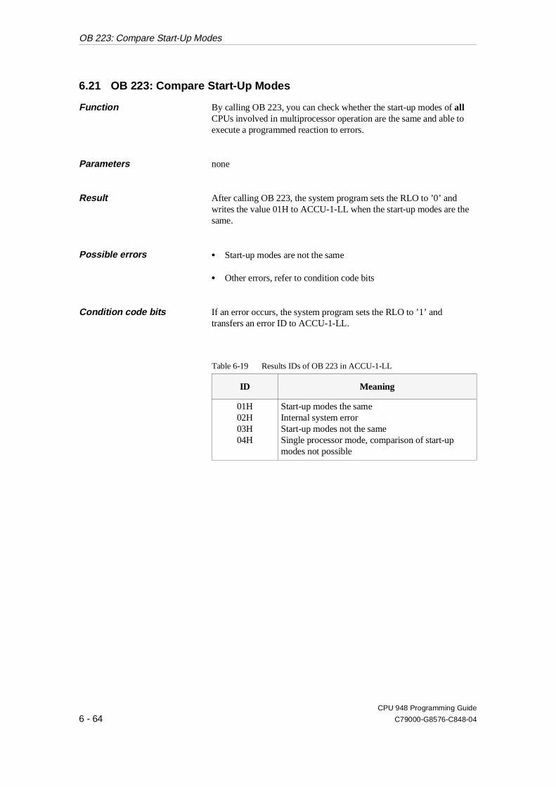
6.21 OB 223: Compare Start-Up Modes
Function By calling OB 223, you can check whether the start-up modes of allCPUs involved in multiprocessor operation are the same and able toexecute a programmed reaction to errors.
Parameters none
Result After calling OB 223, the system program sets the RLO to ’0’ andwrites the value 01H to ACCU-1-LL when the start-up modes are thesame.
Possible errors •• Start-up modes are not the same
•• Other errors, refer to condition code bits
Condition code bits If an error occurs, the system program sets the RLO to ’1’ andtransfers an error ID to ACCU-1-LL.
ID Meaning
01H02H03H04H
Start-up modes the sameInternal system errorStart-up modes not the sameSingle processor mode, comparison of start-upmodes not possible
Table 6-19 Results IDs of OB 223 in ACCU-1-LL
OB 223: Compare Start-Up Modes
CPU 948 Programming Guide
6 - 64 C79000-G8576-C848-04
6.22 OB 254/255: Copy/Duplicate Data Blocks
With the special functions OB 254/255, you copy individual datablocks from a memory card to the user memory or duplicate individualdata blocks within the user memory. The special function OB 254 and OB 255 work identically, withOB 254 exclusively for DX data blocks and OB 255 for DB datablocks.
NoteDuring the copying or duplication, the user interrupts are blocked.No timed interrupts or process interrupts are accepted.
Application Copying data blocks from the memory card or duplicating data blocksin the user memory and assigning a new block number.
Copying
Conditions By using the "copy" function of the two special function OBs(OB 254 or OB 255 call), remember the following conditions:
•• The memory card must be plugged in before the OVERALLRESET and must not be removed afterwards
•• The destination data block must not yet exist
•• The online function "compress memory" must not be active
Function A data block is copied from the memory card to the user memory andretains its original block number. The start address is entered in theaddress list in DB 0.
OB 254/255: Copy/Duplicate Data Blocks
CPU 948 Programming Guide
C79000-G8576-C848-04 6 - 65
Parameters 1. ACCU-1-LL
Number of the block to be copied.
The following block numbers are possible:
Block type Block number
DB (OB 255)DX (OB 254)
3 to 2553 to 255
2. ACCU-1-LH
ACCU-1-LH must be zero.
Duplicating
Function A data block is duplicated within the user memory and it is assigned adifferent block number. The start address of the new data block isentered in the address list in DB 0. The start address of the old block isretained, i.e. the original data block remains valid.
The start address is entered in DB 0 only after the transfer iscompleted and all the IDs are correctly entered in the block header.The duplicated block is therefore only declared valid or existent by thesystem program after it has been completely transferred.
Parameters 1. ACCU-1-LL
Number of the block to be duplicated (source).
2. ACCU-1-LH
Number of the new block (destination).
The following block numbers are possible:
Block type Block number
DB (OB 255)DX (OB 254)
3 to 2553 to 255
OB 254/255: Copy/Duplicate Data Blocks
CPU 948 Programming Guide
6 - 66 C79000-G8576-C848-04
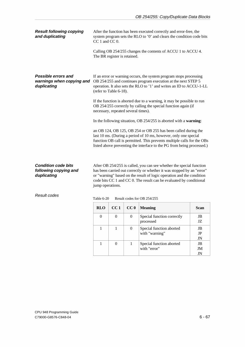
Result following copyingand duplicating
After the function has been executed correctly and error-free, thesystem program sets the RLO to ’0’ and clears the condition code bitsCC 1 and CC 0.
Calling OB 254/255 changes the contents of ACCU 1 to ACCU 4.The BR register is retained.
Possible errors andwarnings when copying andduplicating
If an error or warning occurs, the system program stops processingOB 254/255 and continues program execution at the next STEP 5operation. It also sets the RLO to ’1’ and writes an ID to ACCU-1-LL(refer to Table 6-18).
If the function is aborted due to a warning, it may be possible to runOB 254/255 correctly by calling the special function again (ifnecessary, repeated several times).
In the following situation, OB 254/255 is aborted with a warning:
an OB 124, OB 125, OB 254 or OB 255 has been called during thelast 10 ms. (During a period of 10 ms, however, only one specialfunction OB call is permitted. This prevents multiple calls for the OBslisted above preventing the interface to the PG from being processed.)
Condition code bitsfollowing copying andduplicating
After OB 254/255 is called, you can see whether the special functionhas been carried out correctly or whether it was stopped by an "error"or "warning" based on the result of logic operation and the conditioncode bits CC 1 and CC 0. The result can be evaluated by conditionaljump operations.
Result codes
RLO CC 1 CC 0 Meaning Scan
0 0 0 Special function correctlyprocessed
JBJZ
1 1 0 Special function abortedwith "warning"
JBJPJN
1 0 1 Special function abortedwith "error"
JBJMJN
Table 6-20 Result codes for OB 254/255
OB 254/255: Copy/Duplicate Data Blocks
CPU 948 Programming Guide
C79000-G8576-C848-04 6 - 67

IDs in ACCU-1-LL The system program sets IDs in ACCU-1-LL which specify the causesof a warning or error in more detail.
Bit no. 7 6 5 0
W E Cause of error/warning
The following group codes apply:
Bit no. 7 (W) = 1:warningBit no. 6 (E) = 1:error
ID Meaning
01H Function correctly executed
41H43H48H4AH4BH4CH
4DH4EH
Error:Block header on memory card invalidNot enough memory spaceSource data block does not existBlock number or type illegal/source DBBlock number or type illegal/destination DBDestination data block already exists in the usermemoryOnline function COMPRESS MEMORY activeNo memory card plugged in
8DH
8EH
Warnings:Conflict with an online function except "compressmemory"10 ms waiting time not yet elapsed
Examples
Table 6-21 Result IDs for OB 254/255 in ACCU-1-LL
1. "Copy" :
:L KY 0,120 This sequence of operations copies:JU OB 254 the data block DX 120 from the: memory card to the user memory:
2. "Duplicate":
:L KY 80,85 This sequence of operations :JU OB 255 duplicates data block DB 85; the: new data block has the number 80.: The contents of DB 80 and DB 85: are identical.:
OB 254/255: Copy/Duplicate Data Blocks
CPU 948 Programming Guide
6 - 68 C79000-G8576-C848-04
Contents of Chapter 7
7.1 Application . . . . . . . . . . . . . . . . . . . . . . . . . . . . . . . . . . . . . . . . . . . . . . . . . . . . . . . . . . . . . 7 - 4
7.2 Structure of DX 0 . . . . . . . . . . . . . . . . . . . . . . . . . . . . . . . . . . . . . . . . . . . . . . . . . . . . . . . . 7 - 5
7.2.1 Example of Input in DX 0 . . . . . . . . . . . . . . . . . . . . . . . . . . . . . . . . . . . . . . . . . . . . . . . . . 7 - 7
7.3 Parameters for DX 0 . . . . . . . . . . . . . . . . . . . . . . . . . . . . . . . . . . . . . . . . . . . . . . . . . . . . . 7 - 8
7.4 Examples of Parameter Assignment. . . . . . . . . . . . . . . . . . . . . . . . . . . . . . . . . . . . . . . . . 7 - 12
7.4.1 STEP 5 Programming. . . . . . . . . . . . . . . . . . . . . . . . . . . . . . . . . . . . . . . . . . . . . . . . . . . . 7 - 127.4.2 Parameter Assignment using the PG Screen Form . . . . . . . . . . . . . . . . . . . . . . . . . . . . . 7 - 14
7Extended Data Block DX 0
CPU 948 Programming Guide
C79000-G8576-C848-04 7 - 1

Contents
CPU 948 Programming Guide
7 - 2 C79000-G8576-C848-04
7Extended Data Block DX 0
The following chapter explains how to use the data block DX 0 andhow it is structured. You will find information about the meaning ofthe various DX 0 parameters and will learn how to create and how toassign parameters for a DX 0 data block based on examples.
CPU 948 Programming Guide
C79000-G8576-C848-04 7 - 3
7.1 Application
You can adapt certain system program functions to meet your ownrequirements by selecting alternative defaults in DX 0 compared to thestandard defaults (marked in the parameter table by "D").
The defaults of the system program (D) are automatically set duringeach COLD RESTART and DX 0 is then evaluated. If you have notassigned parameters in DX 0 and loaded it, the defaults remain valid;otherwise the defaults you have selected in DX 0 become the validsettings.
You can make settings in DX 0 by programming the values just as inany normal data block (refer to Section 7.2 to 7.4.1) or using the PGsystem software S5-DOS from Version 3.0 onwards, you can enter thevalues as parameters in a special screen form on your PG (refer toSection 7.4.2).You can make use of the full range of functions of the DX 0 screenform if the PG software STEP 5/ST, Version 6.3 or STEP 5/MT,Version 6.0 plus the corresponding "Delta diskette CPU 948" isinstalled on your PG.
NoteThe settings or modifications made in DX 0 only become effectivefollowing a COLD RESTART. If a modified DX 0 is read during a COLD RESTART, theunmodified parameter assignments are retained.
Differences compared withthe CPU 946/947
Compared with DX 0 parameter assignment for the CPU 946/947,there are various differences when assigning DX 0 parameters for theCPU 948, as follows:
•• Modes:There is no longer a 150U/155U mode, instead of this, there isnow "interruptability at block boundaries " and"interruptability at operation boundaries".
•• Processing system interrupts:With the CPU 948, you can now also combine "process interruptsvia IB 0 = off" (= system interrupt processing) with"interruptability at block boundaries ".This means that multiprocessor operation is now also possible inthe "interruptability at block boundaries" mode.
•• Additional timed interrupts:If you switch off the mode "process interrupts via IB 0", theadditional timed interrupts the delayed interrupt (OB 6) and theclock-controlled interrupt (OB 9) are available.
Application
CPU 948 Programming Guide
7 - 4 C79000-G8576-C848-04
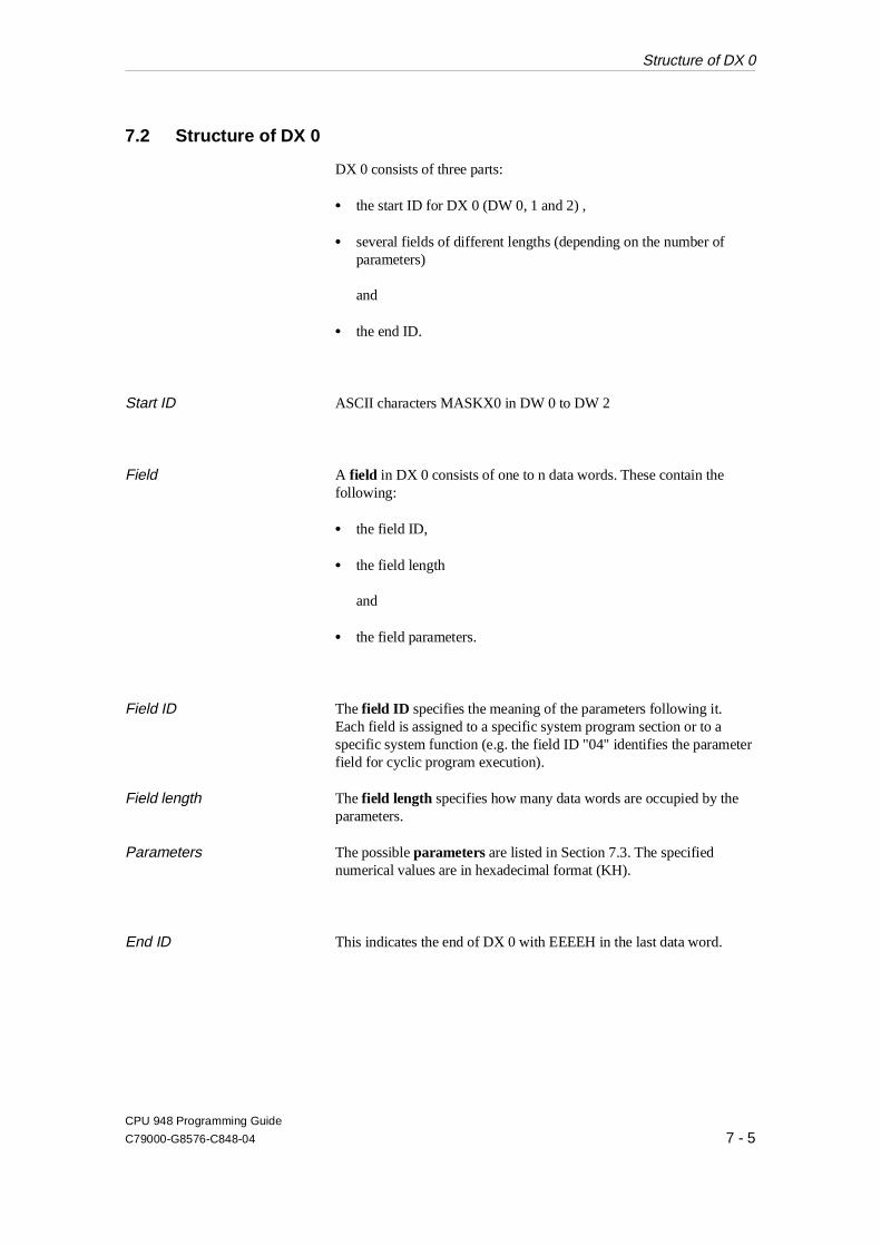
7.2 Structure of DX 0
DX 0 consists of three parts:
•• the start ID for DX 0 (DW 0, 1 and 2) ,
•• several fields of different lengths (depending on the number ofparameters)
and
•• the end ID.
Start ID ASCII characters MASKX0 in DW 0 to DW 2
Field A field in DX 0 consists of one to n data words. These contain thefollowing:
•• the field ID,
•• the field length
and
•• the field parameters.
Field ID The field ID specifies the meaning of the parameters following it.Each field is assigned to a specific system program section or to aspecific system function (e.g. the field ID "04" identifies the parameterfield for cyclic program execution).
Field length The field length specifies how many data words are occupied by theparameters.
Parameters The possible parameters are listed in Section 7.3. The specifiednumerical values are in hexadecimal format (KH).
End ID This indicates the end of DX 0 with EEEEH in the last data word.
Structure of DX 0
CPU 948 Programming Guide
C79000-G8576-C848-04 7 - 5
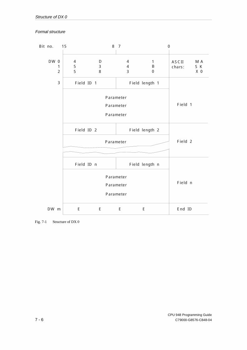
Formal structure
1B0
443
D38
455
Field ID 1 Field length 1
Field ID 2
Field ID n Field length n
Field length 2
Parameter
Parameter
Parameter
Parameter
Parameter
Parameter
ASCIIchars:
Fie ld 1
Field 2
Field n
End ID
15 8 7 0Bit no.
012
3
DW
DW m E E E E
Parameter
M AS KX 0
Fig. 7-1 Structure of DX 0
Structure of DX 0
CPU 948 Programming Guide
7 - 6 C79000-G8576-C848-04
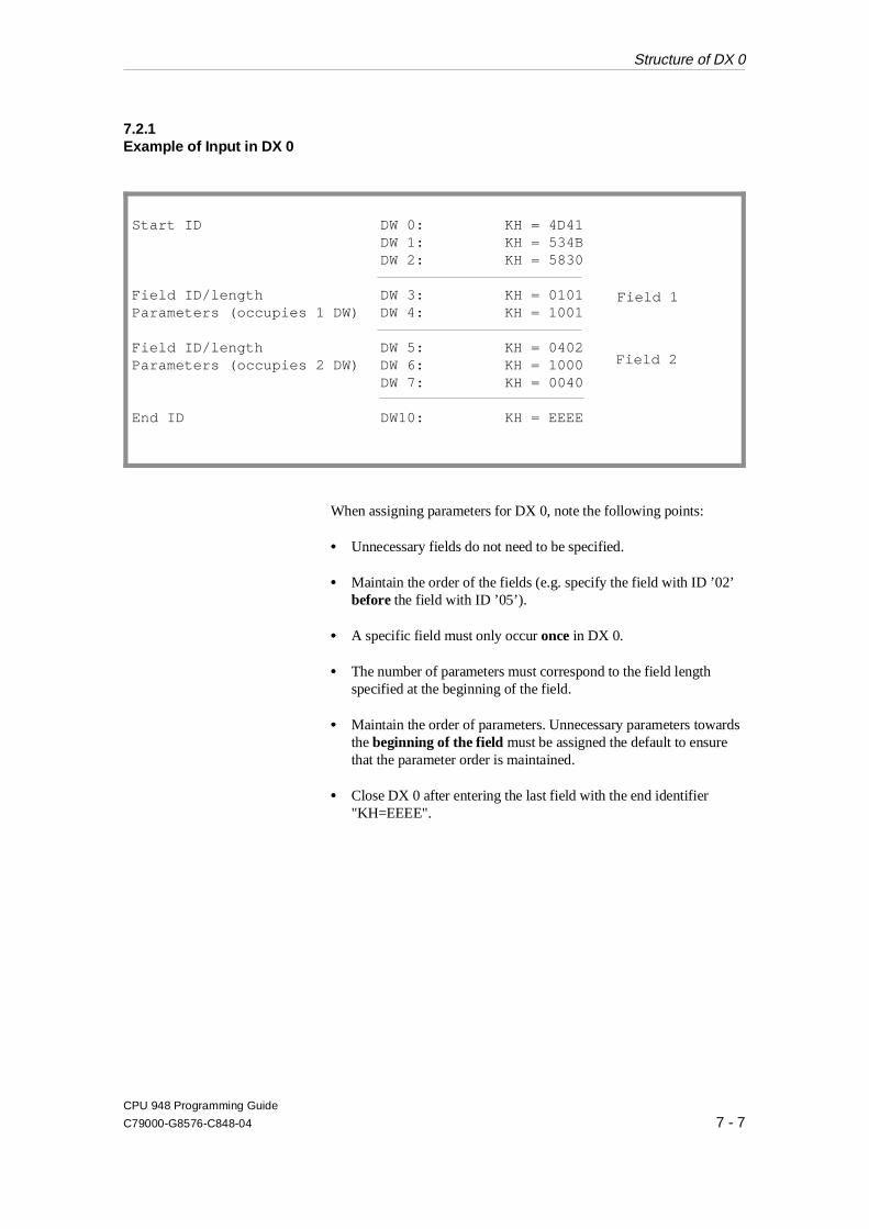
7.2.1Example of Input in DX 0
When assigning parameters for DX 0, note the following points:
•• Unnecessary fields do not need to be specified.
•• Maintain the order of the fields (e.g. specify the field with ID ’02’before the field with ID ’05’).
•• A specific field must only occur once in DX 0.
•• The number of parameters must correspond to the field lengthspecified at the beginning of the field.
•• Maintain the order of parameters. Unnecessary parameters towardsthe beginning of the field must be assigned the default to ensurethat the parameter order is maintained.
•• Close DX 0 after entering the last field with the end identifier"KH=EEEE".
Start ID DW 0: KH = 4D41DW 1: KH = 534B DW 2: KH = 5830
Field ID/length DW 3: KH = 0101Parameters (occupies 1 DW) DW 4: KH = 1001
Field ID/length DW 5: KH = 0402 Parameters (occupies 2 DW) DW 6: KH = 1000
DW 7: KH = 0040
End ID DW10: KH = EEEE
Field 1
Field 2
Structure of DX 0
CPU 948 Programming Guide
C79000-G8576-C848-04 7 - 7
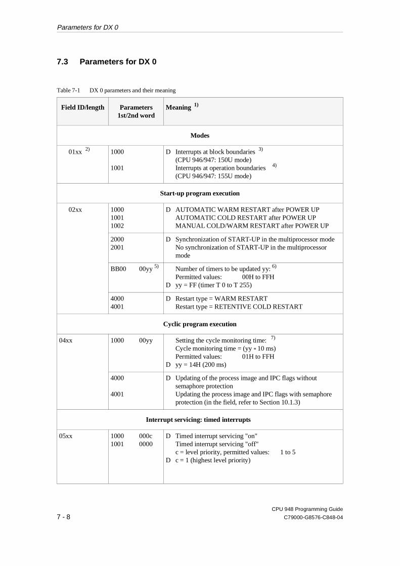
7.3 Parameters for DX 0
Field ID/length Parameters1st/2nd word
Meaning 1)
Modes
01xx 2) 1000
1001
D Interrupts at block boundaries 3)
(CPU 946/947: 150U mode)Interrupts at operation boundaries 4)
(CPU 946/947: 155U mode)
Start-up program execution
02xx 100010011002
D AUTOMATIC WARM RESTART after POWER UPAUTOMATIC COLD RESTART after POWER UPMANUAL COLD/WARM RESTART after POWER UP
20002001
D Synchronization of START-UP in the multiprocessor modeNo synchronization of START-UP in the multiprocessor mode
BB00 00yy 5) Number of timers to be updated yy: 6)
Permitted values: 00H to FFHD yy = FF (timer T 0 to T 255)
40004001
D Restart type = WARM RESTARTRestart type = RETENTIVE COLD RESTART
Cyclic program execution
04xx 1000 00yy Setting the cycle monitoring time: 7)
Cycle monitoring time = (yy * 10 ms)Permitted values: 01H to FFH
D yy = 14H (200 ms)
4000
4001
D Updating of the process image and IPC flags withoutsemaphore protectionUpdating the process image and IPC flags with semaphoreprotection (in the field, refer to Section 10.1.3)
Interrupt servicing: timed interrupts
05xx 1000 000c1001 0000
D Timed interrupt servicing "on"Timed interrupt servicing "off"c = level priority, permitted values: 1 to 5
D c = 1 (highest level priority)
Table 7-1 DX 0 parameters and their meaning
Parameters for DX 0
CPU 948 Programming Guide
7 - 8 C79000-G8576-C848-04

Field ID/length Parameters1st/2nd word
Meaning 1)
Table 7-1 continued:
05xx Interrupt servicing: timed interrupts (cont.)
2000 00yy Basic clock rate for timed interrupt servicing:Basic clock rate = (yy * 10 ms)Permitted values: 01H to FFH
D yy = 0A (100 ms)
30003001
D Clock rate distribution according to interval 1 (1, 2, 5, 10)Clock rate distribution according to interval 2 (2n)(Refer to Section 4.5.2)
Interrupt servicing: process interrupts via S5 bus/system interrupts
4000 000c4001 0002
System interrupt X "on"D System interrupt X "off"
c = level priority,Permitted values: 1 to 5X = A, B, C or D
V c = 2 (level priority 2)
(The servicing of system interrupts can also be combined with "interruptability at block boundaries" with the CPU 948.)
5000 000c5001 0002
System interrupt E "on"D System interrupt E "off"
6000 000c6001 0002
System interrupt F "on"D System interrupt F "off"
7000 000c7001 0002
System interrupt G "on"D System interrupt G "off"
8000 000c8001 0000
D Process interrupts via IB 0 "off"Process interrupts via IB 0 "on"c = level priority, permitted values 1 to 2
D c = 2 (level priority 2)When "process interrupts via IB 0 = on":- only single processor mode,- only "interruptability at block boundaries".
EEEE End ID
1) D = default with DX 0 not loaded or not present.
2) xx = field length (number of data words occupied by the parameters).
3) With the CPU 948, can also be combined with a system interrupt.
4) Must not be combined with process interrupts via IB 0.
5) When specifying the field length, the value "2" must be taken into account for parameters occupying two data words.
6) For updating the timers, please read the explanation on the following page.
7) Set cycle monitoring time with OB 31 or DX 0: If the cycle monitoring time is set both with OB 31 and with DX 0, the system program uses the setting made in OB 31 since it has already evaluated DX 0. For this reason, you should only use one of these possibilities. We recommend setting the cycle monitoring time using DX 0.
Parameters for DX 0
CPU 948 Programming Guide
C79000-G8576-C848-04 7 - 9
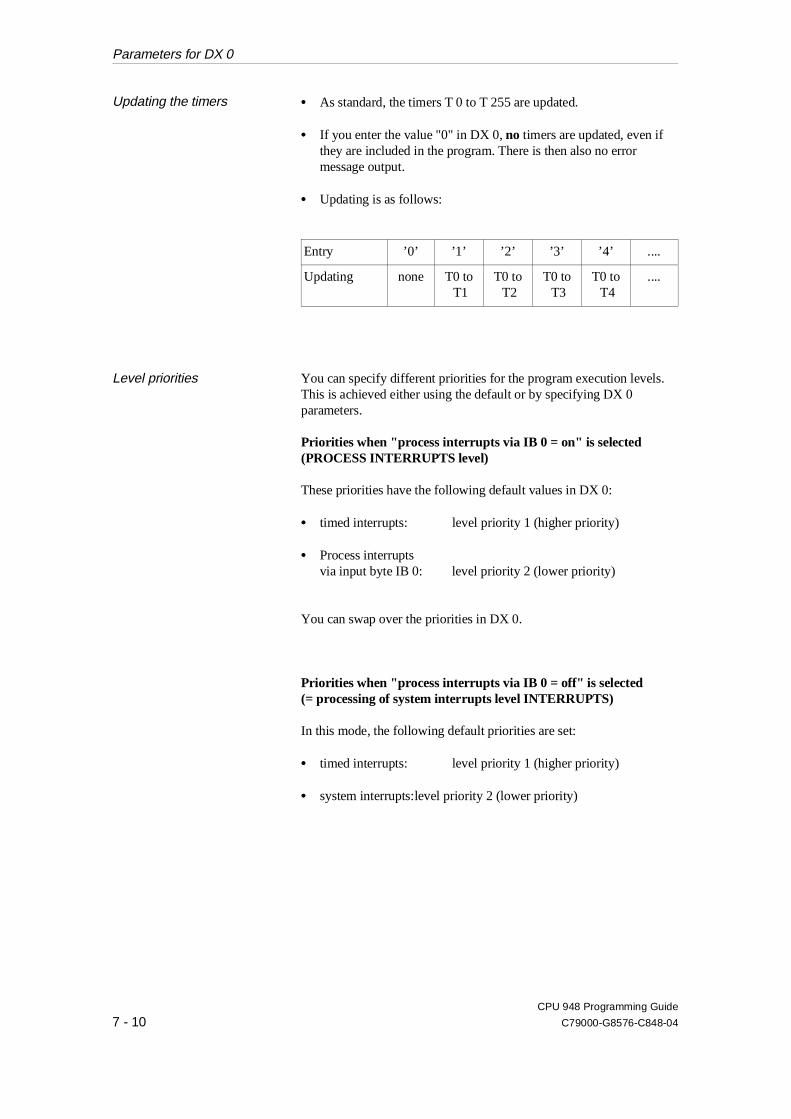
Updating the timers •• As standard, the timers T 0 to T 255 are updated.
•• If you enter the value "0" in DX 0, no timers are updated, even ifthey are included in the program. There is then also no errormessage output.
•• Updating is as follows:
Entry ’0’ ’1’ ’2’ ’3’ ’4’ ....
Updating none T0 to T1
T0 to T2
T0 to T3
T0 to T4
....
Level priorities You can specify different priorities for the program execution levels.This is achieved either using the default or by specifying DX 0parameters.
Priorities when "process interrupts via IB 0 = on" is selected(PROCESS INTERRUPTS level)
These priorities have the following default values in DX 0:
•• timed interrupts: level priority 1 (higher priority)
•• Process interruptsvia input byte IB 0: level priority 2 (lower priority)
You can swap over the priorities in DX 0.
Priorities when "process interrupts via IB 0 = off" is selected (= processing of system interrupts level INTERRUPTS)
In this mode, the following default priorities are set:
•• timed interrupts: level priority 1 (higher priority)
•• system interrupts:level priority 2 (lower priority)
Parameters for DX 0
CPU 948 Programming Guide
7 - 10 C79000-G8576-C848-04
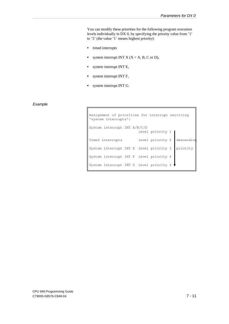
You can modify these priorities for the following program executionlevels individually in DX 0, by specifying the priority value from ’1’to ’5’ (the value ’1’ means highest priority):
•• timed interrupts
•• system interrupt INT X (X = A, B, C or D),
•• system interrupt INT E,
•• system interrupt INT F,
•• system interrupt INT G.
Example
Assignment of priorities for interrupt servicing"system interrupts":
System interrupt INT A/B/C/Dlevel priority 1
Timed interrupts level priority 2 descending
System interrupt INT E level priority 3 priority
System interrupt INT F level priority 4
System interrupt INT G level priority 5
Parameters for DX 0
CPU 948 Programming Guide
C79000-G8576-C848-04 7 - 11

7.4 Examples of Parameter Assignment
7.4.1STEP 5 Programming
Example A:
You want to use three CPUs in the multiprocessor mode: CPU A, B and C. CPUA and B work closely with each other, often exchange data and execute acomplicated start-up program.
CPU C executes a short, time-critical program largely independent of A andB.
As standard, all CPUs operating in the multiprocessor mode start cyclicprogram execution together, i.e. the CPUs wait for each other until theyhave all completed their start-up and then change to cyclic programexecution together.
Since CPU C executes its program independently of the other CPUs and has avery short start-up program , there is no need to synchronize its start-upwith the others. By assigning parameters in DX 0, CPU C can start itscyclic program immediately after completing the start-up without waitingfor CPU A and B.
The parameter for synchronizing the CPUs in the multiprocessor mode is thesecond parameter in the first field. To maintain the order of theparameters, the first parameter for the start up must have the defaultvalue (AUTOMATIC WARM RESTART after POWER UP).
Program DX 0 for CPU C as follows:
DX 0 Start ID "MASKX0" DW 0: KH = 4D41DW 1: KH = 534B DW 2: KH = 5830
1st field ID/length DW 3: KH = 0202Parameter 1 DW 4: KH = 1000Parameter 2 DW 4: KH = 2001End ID DW 5: KH = EEEE
Once you have loaded this DX 0 in the program memory, it becomes effectiveat the next COLD RESTART. Since CPU C runs through a very short start-upprogram and does not wait for A and B, its green RUN LED lights upimmediately following start-up. The BASP signal (disable command output)is, however, only deactivated when all three CPUs have completed theirstart-up. This means that CPU C cannot access the digital I/Os.
Examples of Parameter Assignment
CPU 948 Programming Guide
7 - 12 C79000-G8576-C848-04

Example B:
The parameter assignment for DX 0 shown below achieves the following:
- the mode "interrupts at operation boundaries" is set,
- the timer updating is switched off,
- the cycle time is set to 2.5 seconds,
- the level priority of timed interrupts is set to ’2’
and
- the system interrupt INT E is activated with level priority ’1’.
DX 0 Start ID "MASKX0" DW 0: KH = 4D41 DW 1: KH = 534B DW 2: KH = 5830
1st field ID/length DW 3: KH = 0101Parameters DW 4: KH = 10012nd field ID/length DW 5 KH = 0202Parameters 1) DW 6: KH = BB00
DW 7: KH = 00003rd field ID/length DW 8 KH = 0402Parameters 1) DW 9: KH = 1000
DW10: KH = 00FA 4th field ID/length DW11: KH = 0504Parameters 1) DW12: KH = 1000
DW13: KH = 0002Parameters 1) DW14: KH = 5000
DW15: KH = 0001 End ID DW16: KH = EEEE
This parameter assignment in DX 0 has the following effects on programexecution:
Program execution is interrupted by higher priority levels at operationboundaries instead of at block boundaries.
The runtime of the system program is slightly reduced since no timers areupdated.
A cycle error is only recognized when the runtime of the user program andthe system program together exceeds 2.5 seconds.
No process interrupts from input byte IB 0 are processed, but rather systeminterrupt INT E. Owing to its higher priority, this interrupts timedinterrupt servicing, the processing of the delayed interrupt and theprocessing of a timed job.
1) Under "field length", specify the number of data words occupied by aparameter!
Examples of Parameter Assignment
CPU 948 Programming Guide
C79000-G8576-C848-04 7 - 13

7.4.2Parameter Assignmentusing the PG Screen Form
With the PG system software, screen forms are available for assigningparameters in DX 0 for the CPU 948. The PG software automaticallygenerates data block DX 0 according to the default parameters (valuesin bold face)and parameters you have specified. To assign parametersto DX 0, two screen forms are required.
How to select and complete the PG screen forms is explained in yourSTEP 5 manual.
Structure of the screen forms Two screen forms are required for completing parameter assignmentto DX 0:
The first screen form (Fig. 7-2) contains the parameter groups
- Interruptability,- Restart after power up,- Warm restart procedure,- Number of timer cells,- Cycle time monitoring,- Synchronize multiprocessor restart,- Block transfer of the IPC flags.
DX 0 - param. ass. (S5-155U CPU 948)
Restart after power up:
Interruptability:
(1 = warm restart
(1 = warm restart
2 = cold restart
2 = cold restart with memory)
(0...256)
DX 0
1)
1)
for "interruptability at operation boundaries"
for "interruptability at block boundaries"
Mode 155U
Mode 150U
with older PG-software versions the following is displayed:
(1...255)
3 = manual start)
Warm restart procedure:
Number of timer cells:
Cycle time monitoring (x 10 ms):
Synchronize multiprocessor restart:
Block transfer of the IPC flags:
F1 F2 F3 F4 F5 F6ContinueSelect
F7 F8
1
at block bounds.
1
256
20
YES
NO
Fig. 7-2 PG screen form for assigning parameters to DX 0 / Part 1
Examples of Parameter Assignment
CPU 948 Programming Guide
7 - 14 C79000-G8576-C848-04
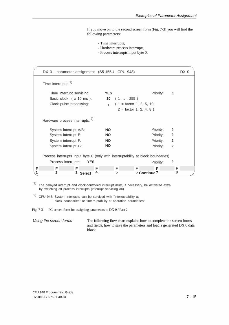
If you move on to the second screen form (Fig. 7-3) you will find thefollowing parameters:
- Time interrupts,- Hardware process interrupts,- Process interrupts input byte 0.
Using the screen forms The following flow chart explains how to complete the screen formsand fields, how to save the parameters and load a generated DX 0 datablock.
DX 0 - parameter assignment (S5-155U CPU 948) DX 0
YES
YES 1
22
22
2
NONO
NONO
Process interrupts:
Process interrupts input byte 0 (only with interruptability at block boundaries)
Hardware process interrupts:
System interrupt G:
System interrupt F:
System interrupt E:System interrupt A/B:
Time interrupts:
Time interrupt servicing:
Priority:
Priority:
Priority:
Priority:
Priority:
Priority:
( 1 . . . 255 )
2)
2) CPU 948: System interrupts can be serviced with "interruptability atblock boundaries" or "interruptability at operation boundaries"
1)
1)The delayed interrupt and clock-controlled interrupt must, if necessary, be activated extraby switching off process interrupts (interrupt servicing on)
( 1 = factor 1, 2, 5, 10
2 = factor 1, 2, 4, 8 )
Basic clock ( x 10 ms ):
Clock pulse processing: 1
10
F1
F2
F3
F4
F5
F6 ContinueSelect
F7
F8
Fig. 7-3 PG screen form for assigning parameters to DX 0 / Part 2
Examples of Parameter Assignment
CPU 948 Programming Guide
C79000-G8576-C848-04 7 - 15
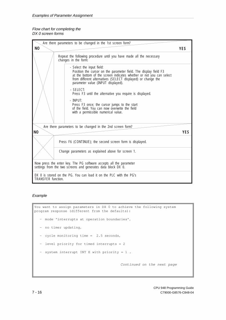
Flow chart for completing theDX 0 screen forms
Example
NO YES
Repeat the following procedure until you have made all the necessarychanges in the form:
Position the cursor on the parameter field. The display field F3at the bottom of the screen indicates whether or not you can selectfrom different alternatives (SELECT displayed) or change theparameter value (INPUT displayed).
Are there parameters to be changed in the 2nd screen form?
Are there parameters to be changed in the 1st screen form?
NO YES
Press F6 (CONTINUE); the second screen form is displayed.
Change parameters as explained above for screen 1.
Now press the enter key. The PG software accepts all the parametersettings from the two screens and generates data block DX 0.
DX 0 is stored on the PG. You can load it on the PLC with the PG’sTRANSFER function.
- Select the input field:
- SELECT:Press F3 until the alternative you require is displayed.
- INPUT:Press F3 once; the cursor jumps to the startof the field. You can now overwrite the fieldwith a permissible numerical value.
You want to assign parameters in DX 0 to achieve the following systemprogram response (different from the defaults):
- mode "interrupts at operation boundaries",
- no timer updating,
- cycle monitoring time = 2.5 seconds,
- level priority for timed interrupts = 2
- system interrupt INT E with priority = 1 .
Continued on the next page
Examples of Parameter Assignment
CPU 948 Programming Guide
7 - 16 C79000-G8576-C848-04
Continuation of the example
Complete the screen form as follows to obtain this response:
First DX 0 screen form:
•• For the MODE parameter, select "interruptability at operation boundaries"with function key F3.
•• For the parameter NUMBER OF TIMER CELLS first press function key F3 andthen type in the number 0 (= no timer).
•• For the CYCLE MONITORING parameter, first press function key F3 and thentype in the number 250 (= 2.5 seconds).
•• Press function key F6 (CONTINUE). The second DX 0 screen form isdisplayed.
Second DX 0 screen form:
•• For the TIMED INTERRUPT/PRIORITY parameter, select the value ’2’ withfunction key F3.
•• For the SYSTEM INTERRUPT E parameter, select the setting ’yes’ withfunction key F3.
•• For the SYSTEM INTERRUPT E/PRIORITY parameter, select the value ’1’ withfunction key F3.
•• For the PROCESS INTERRUPTS parameter, select the setting ’no’ withfunction key F3.
•• Press the enter key to confirm your input. Data block DX 0 is thengenerated by the system software.
Examples of Parameter Assignment
CPU 948 Programming Guide
C79000-G8576-C848-04 7 - 17

Examples of Parameter Assignment
CPU 948 Programming Guide
7 - 18 C79000-G8576-C848-04
Contents of Chapter 8
8.1 Structure of the Memory Area . . . . . . . . . . . . . . . . . . . . . . . . . . . . . . . . . . . . . . . . . . . . . 8 - 4
8.2 Memory Assignment in the CPU 948 . . . . . . . . . . . . . . . . . . . . . . . . . . . . . . . . . . . . . . . . 8 - 5
8.2.1 Memory Assignment for the System RAM . . . . . . . . . . . . . . . . . . . . . . . . . . . . . . . . . . . 8 - 68.2.2 Memory Assignment for the Peripherals . . . . . . . . . . . . . . . . . . . . . . . . . . . . . . . . . . . . . 8 - 8
8.3 User Memory Organization in the CPU 948 . . . . . . . . . . . . . . . . . . . . . . . . . . . . . . . . . . 8 - 10
8.3.1 Block Headers in User Memory. . . . . . . . . . . . . . . . . . . . . . . . . . . . . . . . . . . . . . . . . . . . 8 - 128.3.2 Block Address List in Data Block DB 0 . . . . . . . . . . . . . . . . . . . . . . . . . . . . . . . . . . . . . 8 - 138.3.3 RI/RJ Area. . . . . . . . . . . . . . . . . . . . . . . . . . . . . . . . . . . . . . . . . . . . . . . . . . . . . . . . . . . . . 8 - 148.3.4 RS/RT Area . . . . . . . . . . . . . . . . . . . . . . . . . . . . . . . . . . . . . . . . . . . . . . . . . . . . . . . . . . . . 8 - 158.3.5 Bit Assignment of the System Data Words . . . . . . . . . . . . . . . . . . . . . . . . . . . . . . . . . . . 8 - 188.3.6 Addressable System Data Area . . . . . . . . . . . . . . . . . . . . . . . . . . . . . . . . . . . . . . . . . . . . 8 - 42
8Memory Assignment andMemory Organization
CPU 948 Programming Guide
C79000-G8576-C848-04 8 - 1

Contents
CPU 948 Programming Guide
8 - 2 C79000-G8576-C848-04

8Memory Assignment and Memory Organization
You can use this chapter as a reference section to check on theorganization of the CPU 948 memory. The chapter also includesimportant information contained in some of the system data words.
CPU 948 Programming Guide
C79000-G8576-C848-04 8 - 3
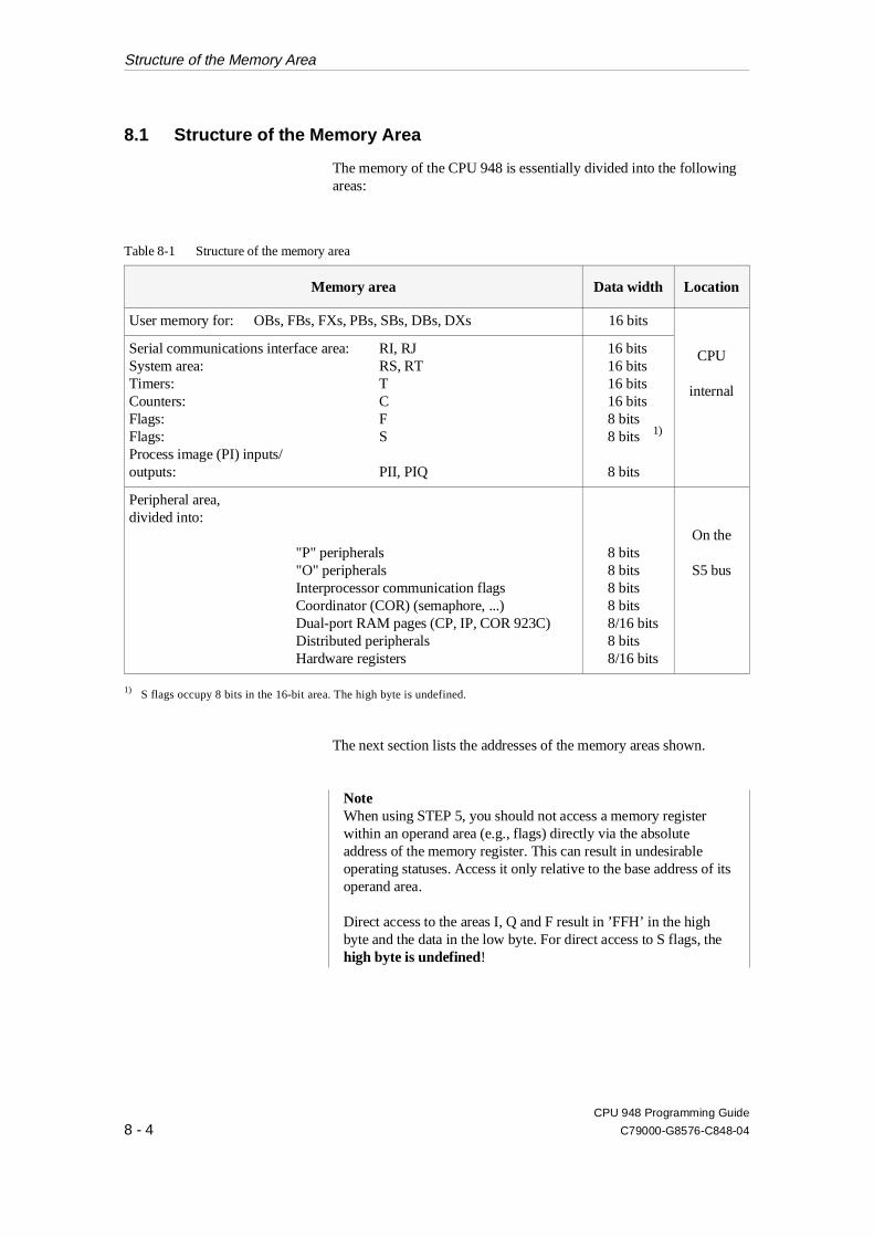
8.1 Structure of the Memory Area
The memory of the CPU 948 is essentially divided into the followingareas:
Memory area Data width Location
User memory for: OBs, FBs, FXs, PBs, SBs, DBs, DXs 16 bits
CPU
internal
Serial communications interface area: RI, RJSystem area: RS, RTTimers: TCounters: CFlags: FFlags: S Process image (PI) inputs/ outputs: PII, PIQ
16 bits16 bits16 bits16 bits8 bits8 bits 1)
8 bits
Peripheral area, divided into:
"P" peripherals"O" peripheralsInterprocessor communication flagsCoordinator (COR) (semaphore, ...)Dual-port RAM pages (CP, IP, COR 923C)Distributed peripheralsHardware registers
8 bits8 bits8 bits8 bits8/16 bits8 bits8/16 bits
On the
S5 bus
1) S flags occupy 8 bits in the 16-bit area. The high byte is undefined.
The next section lists the addresses of the memory areas shown.
NoteWhen using STEP 5, you should not access a memory registerwithin an operand area (e.g., flags) directly via the absoluteaddress of the memory register. This can result in undesirableoperating statuses. Access it only relative to the base address of itsoperand area.
Direct access to the areas I, Q and F result in ’FFH’ in the highbyte and the data in the low byte. For direct access to S flags, thehigh byte is undefined!
Table 8-1 Structure of the memory area
Structure of the Memory Area
CPU 948 Programming Guide
8 - 4 C79000-G8576-C848-04
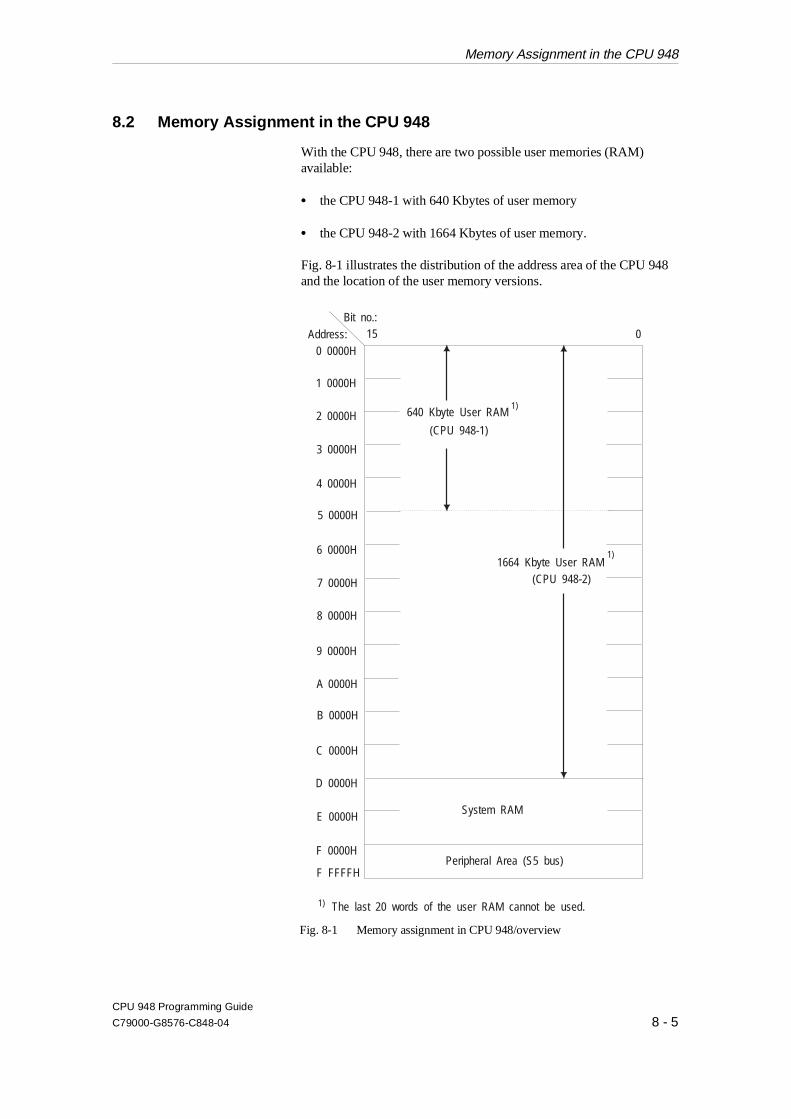
8.2 Memory Assignment in the CPU 948
With the CPU 948, there are two possible user memories (RAM)available:
•• the CPU 948-1 with 640 Kbytes of user memory
•• the CPU 948-2 with 1664 Kbytes of user memory.
Fig. 8-1 illustrates the distribution of the address area of the CPU 948and the location of the user memory versions.
Peripheral Area (S5 bus)
System RAM
The last 20 words of the user RAM cannot be used.
640 Kbyte User RAM
(CPU 948-1)
1664 Kbyte User RAM(CPU 948-2)
Bit no.:
Address:0 0000H
1 0000H
2 0000H
3 0000H
4 0000H
5 0000H
6 0000H
7 0000H
8 0000H
9 0000H
A 0000H
B 0000H
C 0000H
D 0000H
E 0000H
F 0000H
F FFFFH
15 0
1)
1)
1)
Fig. 8-1 Memory assignment in CPU 948/overview
Memory Assignment in the CPU 948
CPU 948 Programming Guide
C79000-G8576-C848-04 8 - 5
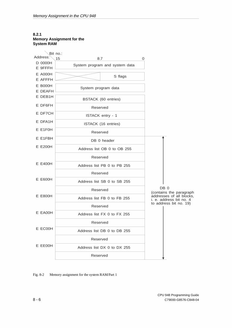
8.2.1Memory Assignment for theSystem RAM
Bit no.:Address:
D 0000HE 9FFFH
E A000H
E AFFFH
E B000H
E DEAFH
E DEB1H
E DF6FH
E DF7CH
E DFA1H
E E1F0H
E E1FBH
E E200H
E E400H
E E600H
E E800H
E EA00H
E EC00H
E EE00H
Reserved
Reserved
Reserved
Reserved
Reserved
Reserved
Reserved
Reserved
Reserved
DB 0 header
DB 0(contains the paragraphaddresses of all blocks,i. e. address bit no. 4to address bit no. 19)
Address list OB 0 to OB 255
Address list PB 0 to PB 255
Address list SB 0 to SB 255
Address list FB 0 to FB 255
Address list FX 0 to FX 255
Address list DB 0 to DB 255
Address list DX 0 to DX 255
ISTACK entry - 1
ISTACK (16 entries)
BSTACK (60 entries)
S flags
System program and system data
System program data
15 8 7 0
Fig. 8-2 Memory assignment for the system RAM/Part 1
Memory Assignment in the CPU 948
CPU 948 Programming Guide
8 - 6 C79000-G8576-C848-04
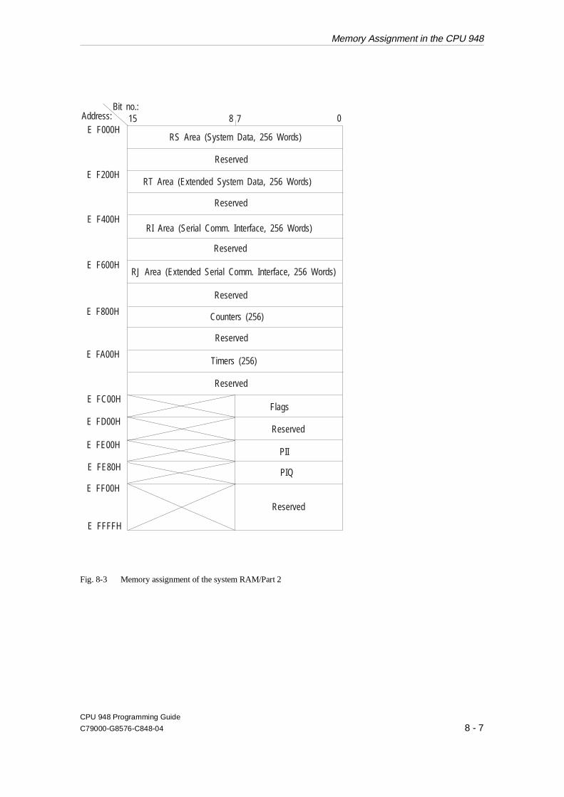
Bit no.:
Address:E F000H
E F200H
E F400H
E F600H
E F800H
E FA00H
E FC00H
E FD00H
E FE00H
E FE80H
E FF00H
E FFFFH
Reserved
Reserved
Reserved
Reserved
Reserved
Reserved
Reserved
Reserved
PII
PIQ
Flags
Counters (256)
Timers (256)
RT Area (Extended System Data, 256 Words)
RJ Area (Extended Serial Comm. Interface, 256 Words)
RI Area (Serial Comm. Interface, 256 Words)
RS Area (System Data, 256 Words)
15 8 7 0
Fig. 8-3 Memory assignment of the system RAM/Part 2
Memory Assignment in the CPU 948
CPU 948 Programming Guide
C79000-G8576-C848-04 8 - 7
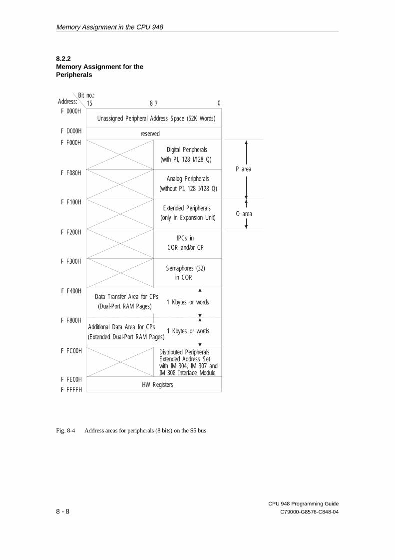
8.2.2Memory Assignment for thePeripherals
Bit no.:Address:
F 0000H
F D000H
F F000H
F F080H
F F100H
F F200H
F F300H
F F400H
F F800H
F FC00H
HW RegistersF FE00H
F FFFFH
reserved
Data Transfer Area for CPs
Additional Data Area for CPs
Distributed PeripheralsExtended Address Setwith IM 304, IM 307 andIM 308 Interface Module
(Dual-Port RAM Pages)1 Kbytes or words
1 Kbytes or words(Extended Dual-Port RAM Pages)
(with PI, 128 I/128 Q)Digital Peripherals
P area
O area
(without PI, 128 I/128 Q)
Analog Peripherals
Extended Peripherals
IPCs in
Semaphores (32)in COR
COR and/or CP
(only in Expansion Unit)
Unassigned Peripheral Address Space (52K Words)
15 8 7 0
Fig. 8-4 Address areas for peripherals (8 bits) on the S5 bus
Memory Assignment in the CPU 948
CPU 948 Programming Guide
8 - 8 C79000-G8576-C848-04
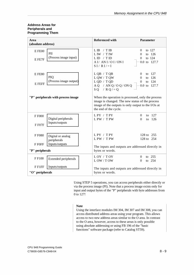
Address Areas forPeripherals andProgramming Them
Using STEP 5 operations, you can access peripherals either directly orvia the process image (PI). Note that a process image exists only forinput and output bytes of the "P" peripherals with byte addresses from 0 to 127!
NoteUsing the interface modules IM 304, IM 307 and IM 308, you canaccess distributed address areas using your program. This allowsaccess to two new address areas similar to the O area. In contrastto the O area, however, access to these areas is only possibleusing absolute addressing or using FB 196 of the "basicfunctions" software package (refer to Catalog ST59).
Area(absolute address)
Referenced with Parameter
"P" peripherals with process image
L IB / T IB 0 to 127L IW / T IW 0 to 126L ID / T ID 0 to 124A I / AN I / O I / ON I 0.0 to 127.7S I / R I / = I
L QB / T QB 0 to 127L QW / T QW 0 to 126L QD / T QD 0 to 124A Q / AN Q / O Q / ON Q 0.0 to 127.7S Q / R Q / = Q
When the operation is processed, only the processimage is changed. The new status of the processimage of the outputs is only output to the I/Os atthe end of the cycle.
"P" peripherals
L PY / T PY 0 to 127L PW / T PW 0 to 126
L PY / T PY 128 to 255L PW / T PW 128 to 254
The inputs and outputs are addressed directly inbytes or words.
"O" peripherals
L OY / T OY 0 to 255L OW / T OW 0 to 254
The inputs and outputs are addressed directly inbytes or words.
PII(Process image input)
PIQ(Process image output)
Digital peripheralsInputs/outputs
Digital or analogperipheralsInputs/outputs
Extended peripherals
Inputs/outputs
E FE00
E FEFF
E FE80
E FE7F
F F000
F F07F
F F080
F F0FF
F F100
F F1FF
Memory Assignment in the CPU 948
CPU 948 Programming Guide
C79000-G8576-C848-04 8 - 9
8.3 User Memory Organization in the CPU 948
Depending on the version of the CPU 948 used, the user memoryoccupies the memory area from 0 0000H to C FFFFH. When youload the individual blocks of your program, they are stored in thememory in random order (with addresses in ascending order).
Block management When you correct a block, the old block in the memory is declaredinvalid (i.e., the start ID is overwritten) and a new block is entered inthe memory and the address list. This also applies when you deleteblocks. The blocks are not really deleted in the memory but simplydeclared invalid. Gaps created by deleting are managed as availablememory locations and are used again when you load new blocks.
Compressing memory The online COMPRESS MEMORY PG function pushes all validblocks in the memory together. When you activate the COMPRESSMEMORY while the CPU is in the STOP mode, all blocks that are notdirectly next to each other are shifted. However, when you activatethis function while the CPU is in the RUN mode, long data andextended data blocks (i.e., longer than 512 data words) are not shiftedbecause of data length consistency. Compressing produces largeavailable memory areas which you can use for loading new blocks.
If the online COMPRESS MEMORY PG function is interrupted (e.g.,when the power is turned off), compressing is terminated and does notresume automatically when power is turned on.
Location of blocks in theuser memory
In the CPU 948, blocks are stored so that data word DW 0 or the firstSTEP 5 statement of each block is located at a paragraph address.Paragraph addresses are at 16-word boundaries. Therefore, all blocksbegin in the memory at the address xxxxBH (bit no. 0 to 3 = BH) andall block bodies at the address yyyy0H (bit no. 0 to 3 = 0H). The gapsthat result between blocks are filled in by invalid data blocks, so thatall blocks continue to exist in consecutive order.
Filler blocks These invalid data blocks are known as "filler blocks". They aretreated in the same way as the other blocks by the memorymanagement and have the following structure:
Start ID: 7070H ;Block type/block number: 01FBH ;DB 251 invalidProgrammer ID: 00FFH ;irrelevantLibrary number: FFFFH ;irrelevantBlock length: 00XXH ;length 5 to 20 wordsData: FFFFH ;according
: ;to: ;length;FFFFH ;can be left out entirely
User Memory Organization in the CPU 948
CPU 948 Programming Guide
8 - 10 C79000-G8576-C848-04
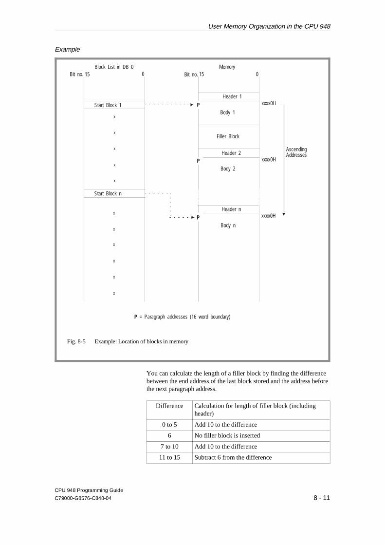
Example
You can calculate the length of a filler block by finding the differencebetween the end address of the last block stored and the address beforethe next paragraph address.
Difference Calculation for length of filler block (includingheader)
0 to 5 Add 10 to the difference
6 No filler block is inserted
7 to 10 Add 10 to the difference
11 to 15 Subtract 6 from the difference
Bit no. Bit no.Block List in DB 0 Memory
Header 1
Header 2
Header n
Body 1
Filler Block
xxxx0H
xxxx0H
AscendingAddresses
xxxx0H
Body 2
Body n
= Paragraph addresses (16 word boundary)
Start Block 1
Start Block n
15 150 0
P
P
P
P
x
x
x
x
x
x
x
x
x
x
x
Fig. 8-5 Example: Location of blocks in memory
User Memory Organization in the CPU 948
CPU 948 Programming Guide
C79000-G8576-C848-04 8 - 11
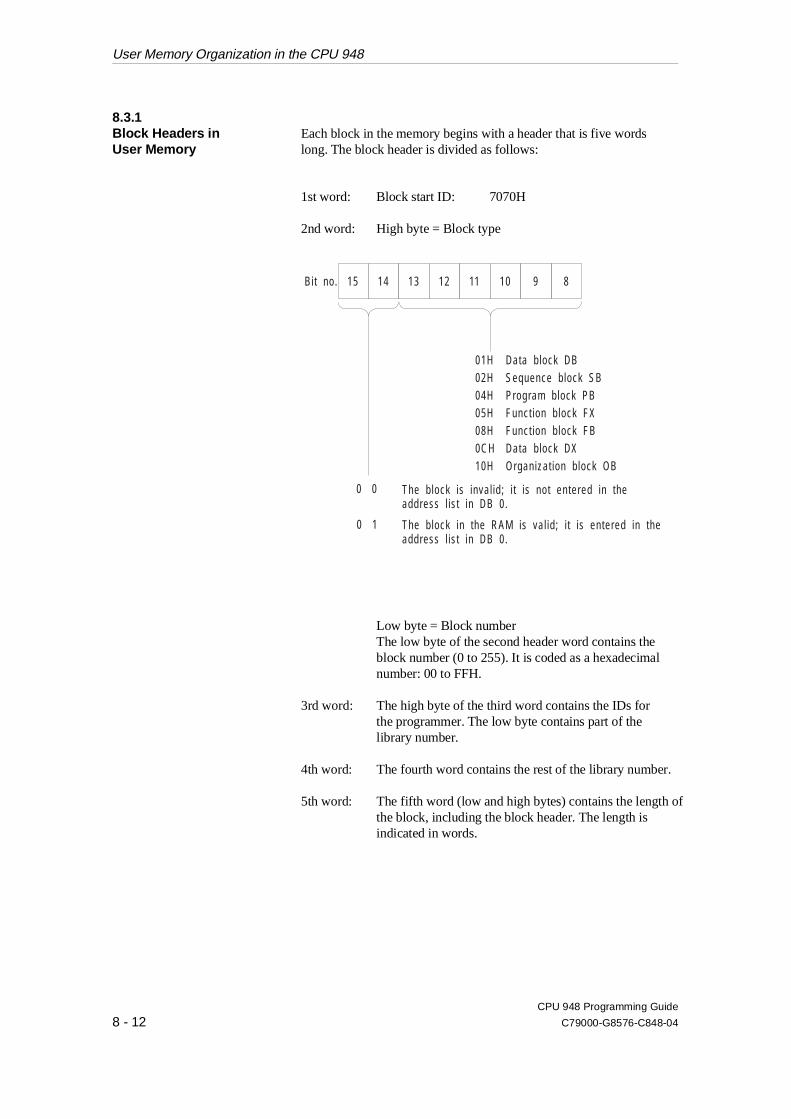
8.3.1Block Headers inUser Memory
Each block in the memory begins with a header that is five wordslong. The block header is divided as follows:
1st word: Block start ID: 7070H
2nd word: High byte = Block type
Low byte = Block numberThe low byte of the second header word contains the block number (0 to 255). It is coded as a hexadecimal number: 00 to FFH.
3rd word: The high byte of the third word contains the IDs for the programmer. The low byte contains part of thelibrary number.
4th word: The fourth word contains the rest of the library number.
5th word: The fifth word (low and high bytes) contains the length ofthe block, including the block header. The length is indicated in words.
01H Data block DB02H Sequence block SB
Program block PBFunct ion block FXFunct ion block FBData block DXOrganizat ion block OB
04H05H08H0CH10H
0 0address l is t in DB 0.
address l is t in DB 0.0 1
The block is inval id; i t is not entered in the
The block in the RAM is val id; i t is entered in the
Bit no. 15 14 13 12 11 10 9 8
User Memory Organization in the CPU 948
CPU 948 Programming Guide
8 - 12 C79000-G8576-C848-04
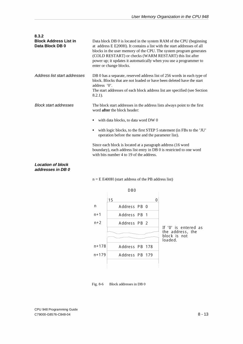
8.3.2Block Address List inData Block DB 0
Data block DB 0 is located in the system RAM of the CPU (beginningat address E E200H). It contains a list with the start addresses of allblocks in the user memory of the CPU. The system program generates(COLD RESTART) or checks (WARM RESTART) this list afterpower up; it updates it automatically when you use a programmer toenter or change blocks.
Address list start addresses DB 0 has a separate, reserved address list of 256 words in each type ofblock. Blocks that are not loaded or have been deleted have the startaddress ’0’.The start addresses of each block address list are specified (see Section8.2.1).
Block start addresses The block start addresses in the address lists always point to the firstword after the block header:
•• with data blocks, to data word DW 0
•• with logic blocks, to the first STEP 5 statement (in FBs to the ’JU’operation before the name and the parameter list).
Since each block is located at a paragraph address (16 wordboundary), each address list entry in DB 0 is restricted to one wordwith bits number 4 to 19 of the address.
Location of blockaddresses in DB 0
n = E E400H (start address of the PB address list)
Address PB 0
Address PB 1
Address PB 2
Address PB 178
Address PB 179
If ’0 ’ is entered asthe address, theblock is notloaded.
DB0
n
n+1
n+2
n+178
n+179
15 0
Fig. 8-6 Block addresses in DB 0
User Memory Organization in the CPU 948
CPU 948 Programming Guide
C79000-G8576-C848-04 8 - 13
Example of how to obtain ablock address
8.3.3RI/RJ Area The RI area is an area that is 256 words long in the internal system
RAM of the CPU. RI occupies addresses E F400H to E F4FFH.
The RJ area is an area that is 256 words long in the internal systemRAM of the CPU. RJ occupies addresses E F600H to E F6FFH.
You can use the entire RI area (RI 0 to RI 255) and the entire RJ area(RJ 0 to RJ 255) for your own purposes.
The RI/RJ area is only filled with zeros following OVERALL RESET.
The block start addresses of the program blocksare located in DB 0 and begin at address E E400H.The start address of PB 22 can therefore be readout by accessing memory at address E E416H(= start address of the PB + 16H).
User Memory Organization in the CPU 948
CPU 948 Programming Guide
8 - 14 C79000-G8576-C848-04
8.3.4RS/RT Area The RS and RT areas contain information for the system programmer and
system internal data.
The RS area is an area that is 256 words long in the internal systemRAM of the CPU. RS occupies addresses E F000H to E F0FFH.
CautionYou should only write to system data words RS 60 to RS 63:
All other system data should only be read:
Writing to the system data area can affect the functional capabilityof your programmable controller and connected programmers:serious disturbances can occur which may put both people andmachines in danger.
The RT area is an area that is 256 words long in the internal systemRAM of the CPU. RT occupies addresses E F200H to E F2FFH.
You can use the whole RT area (RT 0 to RT 255) for your ownpurposes if
1. you do not use standard FBs
and
2. you do not use PG functions via SINEC H1 and the parallel S5 bus.
Only an overall reset can clear the RS/RT areas.
RS/RT Area
CPU 948 Programming Guide
C79000-G8576-C848-04 8 - 15

Using the online function SYSTEM PARAMETERS, you can obtainthe information contained in some of the system data (about theinternal structure of the CPU, the software release, the CPU identifieretc.)
Assignment of the RS area
RS Name Address
0 Input byte IB 0 image table(external process interrupts)
E F000H
1 External process interrupts in theprocessing queue (IB 0)
E F001H
2 to 4 System program
5 Current cycle time E F005H
6 System program
7 STOP mode ID (ISTACK) E F007H
8 Start/restart IDs (ISTACK) E F008H
9 to15 System program
16 Error area: output bytes 0 to 15 E F010H
17 to 23 Error area: output bytes 16 to 127E F011H
toE F017H
24 to 31 Error area: input bytes 0 to 127E F018H
toE F01FH
32 to 47 Error area: interprocessor communication flag bytes 0 to 255
E F020Hto
E F02FH
48 to 49 System program
50 PAFE byte for "backplane bus functions" E F032H
51 to 59 System program
60 to 63 Available to userE F03CH
toE F03FH
64 to 67 System program
68 to 71 Error address with QVZ and PARE errorsE F044H
toE F047H
72 to 74 System program
Table 8-2 Assignment of the RS area
RS/RT Area
CPU 948 Programming Guide
8 - 16 C79000-G8576-C848-04
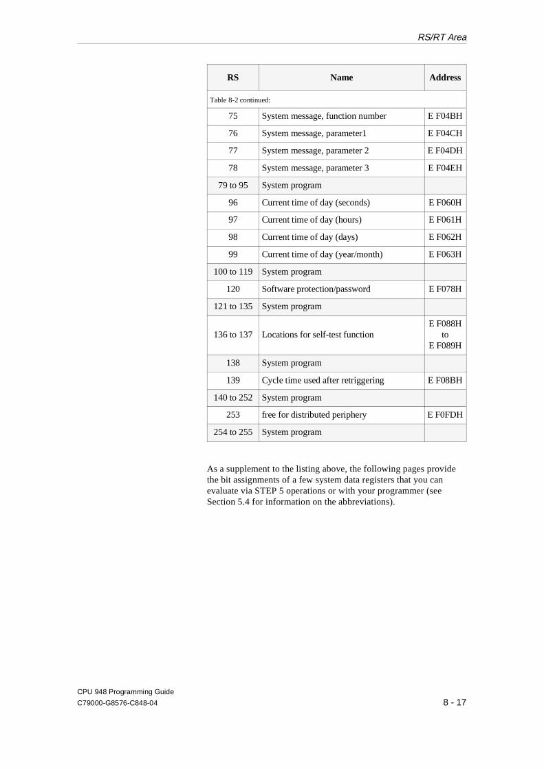
RS Name Address
Table 8-2 continued:
75 System message, function number E F04BH
76 System message, parameter1 E F04CH
77 System message, parameter 2 E F04DH
78 System message, parameter 3 E F04EH
79 to 95 System program
96 Current time of day (seconds) E F060H
97 Current time of day (hours) E F061H
98 Current time of day (days) E F062H
99 Current time of day (year/month) E F063H
100 to 119 System program
120 Software protection/password E F078H
121 to 135 System program
136 to 137 Locations for self-test functionE F088H
toE F089H
138 System program
139 Cycle time used after retriggering E F08BH
140 to 252 System program
253 free for distributed periphery E F0FDH
254 to 255 System program
As a supplement to the listing above, the following pages providethe bit assignments of a few system data registers that you canevaluate via STEP 5 operations or with your programmer (seeSection 5.4 for information on the abbreviations).
RS/RT Area
CPU 948 Programming Guide
C79000-G8576-C848-04 8 - 17
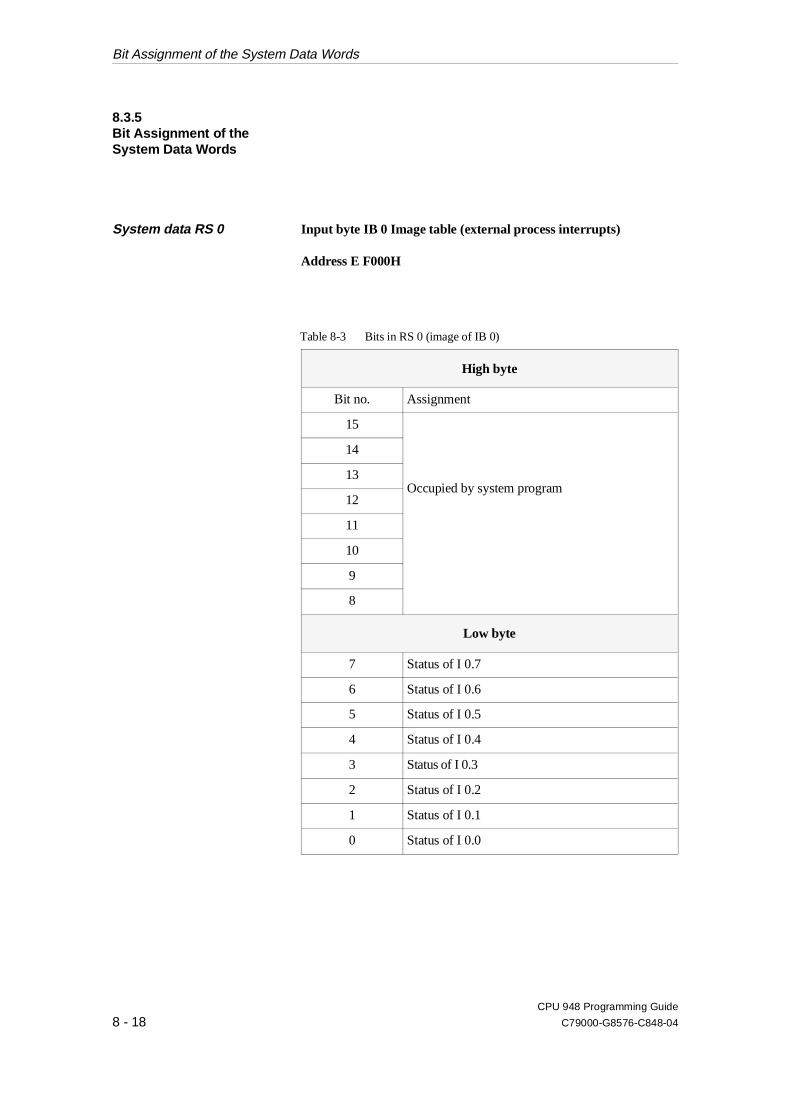
8.3.5Bit Assignment of theSystem Data Words
System data RS 0 Input byte IB 0 Image table (external process interrupts)
Address E F000H
High byte
Bit no. Assignment
15
Occupied by system program
14
13
12
11
10
9
8
Low byte
7 Status of I 0.7
6 Status of I 0.6
5 Status of I 0.5
4 Status of I 0.4
3 Status of I 0.3
2 Status of I 0.2
1 Status of I 0.1
0 Status of I 0.0
Table 8-3 Bits in RS 0 (image of IB 0)
Bit Assignment of the System Data Words
CPU 948 Programming Guide
8 - 18 C79000-G8576-C848-04

System data RS 1 Condition code of external process interrupts currently inprocessing queue
Address: E F001H
High byte
Bit no. Assignment
15
All the bits have the value ’0’
14
13
12
11
10
9
8
Low byte
7 Bit = ’1’: edge I 0.7
6 Bit = ’1’: edge I 0.6
5 Bit = ’1’: edge I 0.5
4 Bit = ’1’: edge I 0.4
3 Bit = ’1’: edge I 0.3
2 Bit = ’1’: edge I 0.2
1 Bit = ’1’: edge I 0.1
0 Bit = ’1’: edge I 0.0
Table 8-4 Bits of RS 1 (current process interrupts)
Bit Assignment of the System Data Words
CPU 948 Programming Guide
C79000-G8576-C848-04 8 - 19
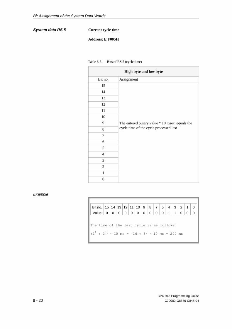
System data RS 5 Current cycle time
Address: E F005H
High byte and low byte
Bit no. Assignment
15
The entered binary value * 10 msec. equals thecycle time of the cycle processed last
14
13
12
11
10
9
8
7
6
5
4
3
2
1
0
Example
Table 8-5 Bits of RS 5 (cycle time)
Bit no. 15 14 13 12 11 10 9 8 7 5 4 3 2 1 0
Value 0 0 0 0 0 0 0 0 0 0 1 1 0 0 0
The time of the last cycle is as follows:
(2 4 + 2 3) * 10 ms = (16 + 8) * 10 ms = 240 ms
Bit Assignment of the System Data Words
CPU 948 Programming Guide
8 - 20 C79000-G8576-C848-04

System data RS 7 Programmable controller STOP mode IDs (ISTACK)
Address: E F007H
High byte
Bit no. Assignment
15Reserved
14
13
12 Faulty ISTACK level
11 Illegal start-up type (UANL)
10 Interruption in stop loop
9 Illegal call of system block (SYSFHL)
8 Error in start-up block (AFEL)
Low byte
7 Interruption by system (USYS –warm restartpossible)
6 Interruption by programming error(UPROG – cold restart)
5 "End of program test" (BEARBE)
4 Stop switch (STOPS)
3 End of operation stop (STS)
2 End of cycle stop (STP)
1 Multiprocessing stop (HALT)
0 PG stop (PGSTP)
Table 8-6 Bits of RS 7 (PLC stop IDs)
Bit Assignment of the System Data Words
CPU 948 Programming Guide
C79000-G8576-C848-04 8 - 21
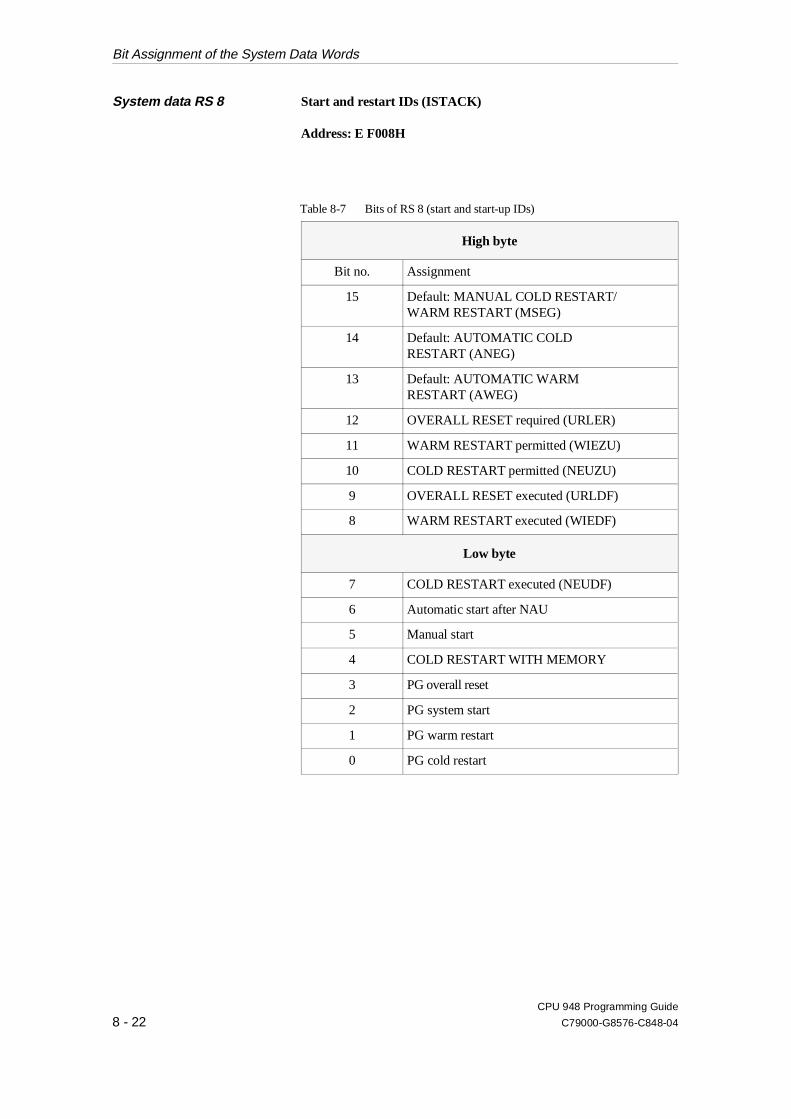
System data RS 8 Start and restart IDs (ISTACK)
Address: E F008H
High byte
Bit no. Assignment
15 Default: MANUAL COLD RESTART/WARM RESTART (MSEG)
14 Default: AUTOMATIC COLDRESTART (ANEG)
13 Default: AUTOMATIC WARMRESTART (AWEG)
12 OVERALL RESET required (URLER)
11 WARM RESTART permitted (WIEZU)
10 COLD RESTART permitted (NEUZU)
9 OVERALL RESET executed (URLDF)
8 WARM RESTART executed (WIEDF)
Low byte
7 COLD RESTART executed (NEUDF)
6 Automatic start after NAU
5 Manual start
4 COLD RESTART WITH MEMORY
3 PG overall reset
2 PG system start
1 PG warm restart
0 PG cold restart
Table 8-7 Bits of RS 8 (start and start-up IDs)
Bit Assignment of the System Data Words
CPU 948 Programming Guide
8 - 22 C79000-G8576-C848-04
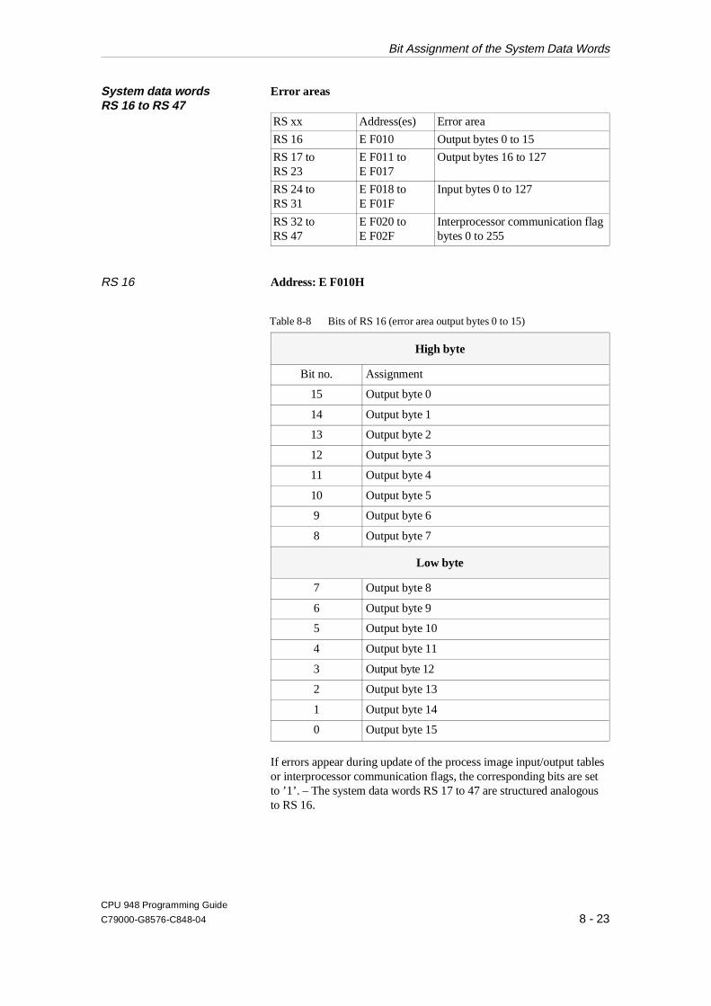
System data wordsRS 16 to RS 47
Error areas
RS xx Address(es) Error area
RS 16 E F010 Output bytes 0 to 15
RS 17 toRS 23
E F011 toE F017
Output bytes 16 to 127
RS 24 toRS 31
E F018 toE F01F
Input bytes 0 to 127
RS 32 toRS 47
E F020 toE F02F
Interprocessor communication flagbytes 0 to 255
RS 16 Address: E F010H
High byte
Bit no. Assignment
15 Output byte 0
14 Output byte 1
13 Output byte 2
12 Output byte 3
11 Output byte 4
10 Output byte 5
9 Output byte 6
8 Output byte 7
Low byte
7 Output byte 8
6 Output byte 9
5 Output byte 10
4 Output byte 11
3 Output byte 12
2 Output byte 13
1 Output byte 14
0 Output byte 15
If errors appear during update of the process image input/output tablesor interprocessor communication flags, the corresponding bits are setto ’1’. – The system data words RS 17 to 47 are structured analogousto RS 16.
Table 8-8 Bits of RS 16 (error area output bytes 0 to 15)
Bit Assignment of the System Data Words
CPU 948 Programming Guide
C79000-G8576-C848-04 8 - 23
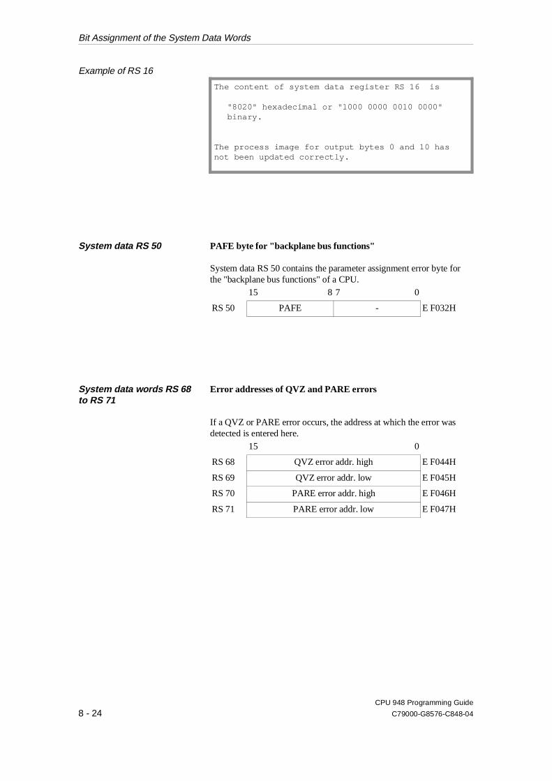
Example of RS 16
System data RS 50 PAFE byte for "backplane bus functions"
System data RS 50 contains the parameter assignment error byte forthe "backplane bus functions" of a CPU.
15 8 7 0
RS 50 PAFE - E F032H
System data words RS 68to RS 71
Error addresses of QVZ and PARE errors
If a QVZ or PARE error occurs, the address at which the error wasdetected is entered here.
15 0
RS 68 QVZ error addr. high E F044H
RS 69 QVZ error addr. low E F045H
RS 70 PARE error addr. high E F046H
RS 71 PARE error addr. low E F047H
The content of system data register RS 16 is
"8020" hexadecimal or "1000 0000 0010 0000" binary.
The process image for output bytes 0 and 10 hasnot been updated correctly.
Bit Assignment of the System Data Words
CPU 948 Programming Guide
8 - 24 C79000-G8576-C848-04
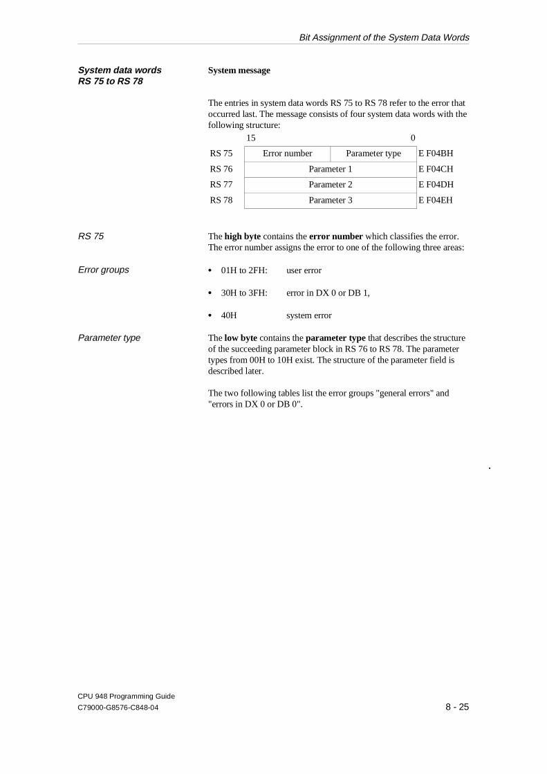
System data words RS 75 to RS 78
System message
The entries in system data words RS 75 to RS 78 refer to the error thatoccurred last. The message consists of four system data words with thefollowing structure:
15 0
RS 75 Error number Parameter type E F04BH
RS 76 Parameter 1 E F04CH
RS 77 Parameter 2 E F04DH
RS 78 Parameter 3 E F04EH
RS 75 The high byte contains the error number which classifies the error.The error number assigns the error to one of the following three areas:
Error groups •• 01H to 2FH: user error
•• 30H to 3FH: error in DX 0 or DB 1,
•• 40H system error
Parameter type The low byte contains the parameter type that describes the structureof the succeeding parameter block in RS 76 to RS 78. The parametertypes from 00H to 10H exist. The structure of the parameter field isdescribed later.
The two following tables list the error groups "general errors" and"errors in DX 0 or DB 0".
Bit Assignment of the System Data Words
CPU 948 Programming Guide
C79000-G8576-C848-04 8 - 25

General errors
Errornumber
Parametertype
Meaning
01H 01H Block called is not loaded
02H 01H Addressing error
03H 01H Cycle time error
04H 01H Substitution error
05H 02H Timeout distributed peripherals
06H 03H Timeout user memory
07H 01H Load/transfer error with data blocksand extended data blocks
08H 01H Bracket counter overflow
09H 04H Data block to be opened does not exist
0AH 05H Error with internal time interrupts/other interrupts
0BH 03H Timeout page frame area
0CH 03H Timeout global communication area
0DH 07H Timeout in process image updating
0EH 03H Timeout in IPC flag synchronization error
0FH 03H Timeout "P"/"O" peripherals
10H 03H Timeout since interface module (IM 3/IM 4)missing
11H 03H Parity error in user memory
12H 01H Timeout process image transfer
13H 01H Timeout input byte IB 0
14H 01H BSTACK overflow
15H 01H STS operation
16H 01H RUN/STOP switch set to STOP position
17H 01H Halt signal from the coordinator
18H 01H Not used
19H 01H Load/transfer error with L BY/T BY(process image update)
1AH 01H Load/transfer error during addressingvia the BR register
1BH 01H I/Os not ready
1CH 08H Timeout/parity error duringinitialization
Table 8-9 RS 75: general errors
Bit Assignment of the System Data Words
CPU 948 Programming Guide
8 - 26 C79000-G8576-C848-04
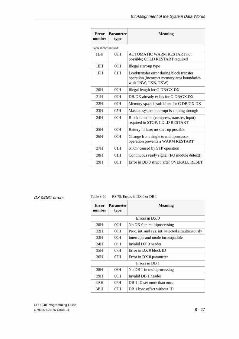
Errornumber
Parametertype
Meaning
Table 8-9 continued:
1DH 08H AUTOMATIC WARM RESTART notpossible; COLD RESTART required
1EH 00H Illegal start-up type
1FH 01H Load/transfer error during block transferoperation (incorrect memory area boundarieswith TNW, TXB, TXW)
20H 09H Illegal length for G DB/GX DX
21H 09H DB/DX already exists for G DB/GX DX
22H 09H Memory space insufficient for G DB/GX DX
23H 05H Masked system interrupt is coming through
24H 00H Block function (compress, transfer, input)required in STOP, COLD RESTART
25H 00H Battery failure; no start-up possible
26H 00H Change from single to multiprocessoroperation prevents a WARM RESTART
27H 01H STOP caused by STP operation
28H 01H Continuous ready signal (I/O module defect))
29H 08H Error in DB 0 struct. after OVERALL RESET
DX 0/DB1 errors
Errornumber
Parametertype
Meaning
Errors in DX 0
30H 00H No DX 0 in multiprocessing
32H 00H Proc. int. and sys. int. selected simultaneously
33H 00H Interrupts and mode incompatible
34H 06H Invalid DX 0 header
35H 07H Error in DX 0 block ID
36H 07H Error in DX 0 parameter
Errors in DB 1
38H 06H No DB 1 in multiprocessing
39H 06H Invalid DB 1 header
3AH 07H DB 1 ID set more than once
3BH 07H DB 1 byte offset without ID
Table 8-10 RS 75: Errors in DX 0 or DB 1
Bit Assignment of the System Data Words
CPU 948 Programming Guide
C79000-G8576-C848-04 8 - 27
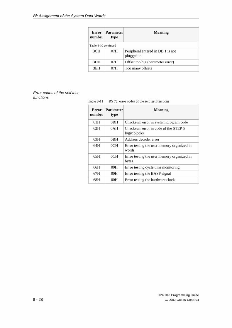
Errornumber
Parametertype
Meaning
Table 8-10 continued
3CH 07H Peripheral entered in DB 1 is notplugged in
3DH 07H Offset too big (parameter error)
3EH 07H Too many offsets
Error codes of the self testfunctions
Errornumber
Parametertype
Meaning
61H 0BH Checksum error in system program code
62H 0AH Checksum error in code of the STEP 5logic blocks
63H 0BH Address decoder error
64H 0CH Error testing the user memory organized inwords
65H 0CH Error testing the user memory organized inbytes
66H 00H Error testing cycle time monitoring
67H 00H Error testing the BASP signal
68H 00H Error testing the hardware clock
Table 8-11 RS 75: error codes of the self test functions
Bit Assignment of the System Data Words
CPU 948 Programming Guide
8 - 28 C79000-G8576-C848-04

Structure of the parameterfield (RS 76 to RS 78)
Parametertype
Structure of the parameter field
00H No parameter; parameter 1, 2, 3 = 0
01H Parameter 1: block type/block number (IDs from block header)
Parameter 2: operation that caused an interruption
02H Parameter 1: interface module number (IM 302) (distributed periphery)
Parameter 2: number of the defective interface
Parameter 3: incorrect byte offset
03H Parameter 1: not used
Parameter 2: error address high
Parameter 3: error address low
04H Parameter 1: block type/block number (IDs from block header)
Parameter 2: operation that caused the interruption
Parameter 3: number of the DB/DX to be opened
05H Parameter 1: The following bits are set depending on the error:
Bit no. 0 = 1: timed interrupt/period 1
Bit no. 1 = 1: timed interrupt/period 2
: : : :
Bit no. 7 = 1: timed interrupt/period 8
Bit no. 8 = 1: timed interrupt/period 9
Bit no. 9 = 1: clock masked (ignored) for too long= 0: queue overflow
Bit no. 10 reserved
Bit no. 11 reserved
Bit no. 12 = 1: interrupt G
Bit no. 13 = 1: interrupt F
Bit no. 14 = 1: interrupt E
Bit no. 15 = 1: interrupt X
06H Parameter 1 data word expected in DX 0 or DB 1 header
Parameter 2 actual data word in DX 0 or DB 1 header
07H Parameter 1 block ID or code word in DX 0 or DB 1
Parameter 2 incorrect parameter 1 in DX 0 or DB 1(FFFFH: parameter irrelevant)
Parameter 3 incorrect parameter 2 in DX 0 or DB 1(FFFFH: parameter irrelevant)
Table 8-12 RS 76 to RS 78: Parameter types
Bit Assignment of the System Data Words
CPU 948 Programming Guide
C79000-G8576-C848-04 8 - 29
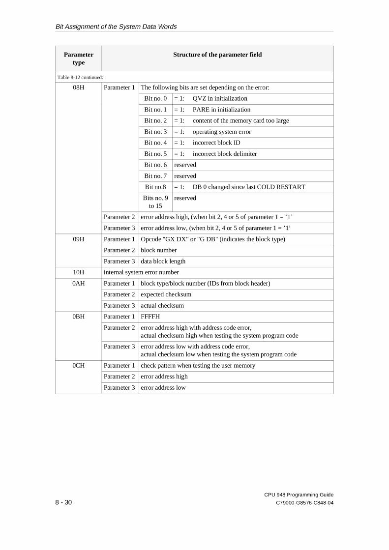
Parametertype
Structure of the parameter field
Table 8-12 continued:
08H Parameter 1 The following bits are set depending on the error:
Bit no. 0 = 1: QVZ in initialization
Bit no. 1 = 1: PARE in initialization
Bit no. 2 = 1: content of the memory card too large
Bit no. 3 = 1: operating system error
Bit no. 4 = 1: incorrect block ID
Bit no. 5 = 1: incorrect block delimiter
Bit no. 6 reserved
Bit no. 7 reserved
Bit no.8 = 1: DB 0 changed since last COLD RESTART
Bits no. 9to 15
reserved
Parameter 2 error address high, (when bit 2, 4 or 5 of parameter 1 = ’1’
Parameter 3 error address low, (when bit 2, 4 or 5 of parameter 1 = ’1’
09H Parameter 1 Opcode "GX DX" or "G DB" (indicates the block type)
Parameter 2 block number
Parameter 3 data block length
10H internal system error number
0AH Parameter 1 block type/block number (IDs from block header)
Parameter 2 expected checksum
Parameter 3 actual checksum
0BH Parameter 1 FFFFH
Parameter 2 error address high with address code error,actual checksum high when testing the system program code
Parameter 3 error address low with address code error,actual checksum low when testing the system program code
0CH Parameter 1 check pattern when testing the user memory
Parameter 2 error address high
Parameter 3 error address low
Bit Assignment of the System Data Words
CPU 948 Programming Guide
8 - 30 C79000-G8576-C848-04
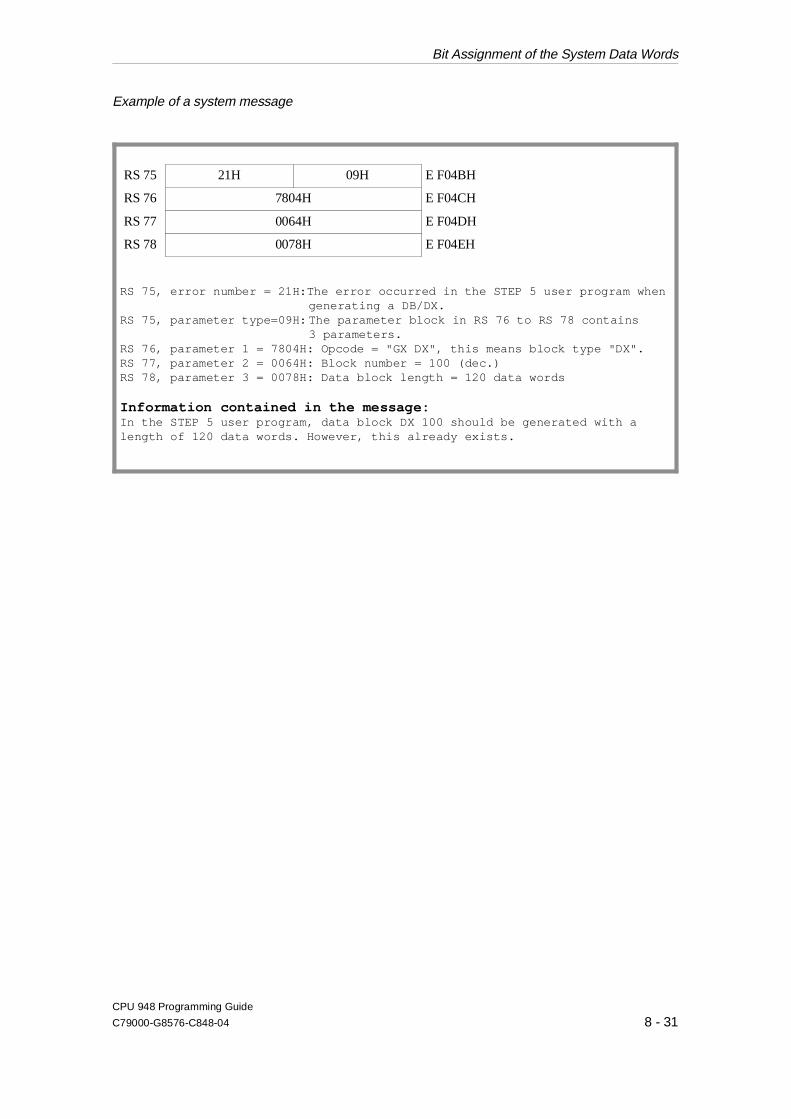
Example of a system message
RS 75 21H 09H E F04BH
RS 76 7804H E F04CH
RS 77 0064H E F04DH
RS 78 0078H E F04EH
RS 75, error number = 21H:The error occurred in the STEP 5 user program whengenerating a DB/DX.
RS 75, parameter type=09H: The parameter block in RS 76 to RS 78 contains 3 parameters.
RS 76, parameter 1 = 7804H: Opcode = "GX DX", this means block type "DX".RS 77, parameter 2 = 0064H: Block number = 100 (dec.)RS 78, parameter 3 = 0078H: Data block length = 120 data words
Information contained in the message: In the STEP 5 user program, data block DX 100 should be generated with alength of 120 data words. However, this already exists.
Bit Assignment of the System Data Words
CPU 948 Programming Guide
C79000-G8576-C848-04 8 - 31

System data wordsRS 96 to RS 99
Real-time clock
The current date and time of day are kept in system data areas RS 96to RS 99 and can if necessary be read out from these locations.
15 0
RS 96 Seconds 1/10, 1/100 seconds E F060H
RS 97 Hours Minutes E F061H
RS 98 Day Day of the week E F062H
RS 99 Year Month E F063H
The clock is updated by a 10 msec. pulse.
RS 96 Seconds and 1/100 seconds (address: E F060H):
High byte
Bit no. Assignment
15Seconds, tens,permitted: 00H to 05H
14
13
12
11Seconds, units,permitted: 00H to 09H
10
9
8
Low byte
71/10 second,permitted: 00H to 09H
6
5
4
31/100 second,permitted: 00H to 09H
2
1
0
Table 8-13 Structure of RS 96 (real-time clock: seconds, 1/100 seconds)
Bit Assignment of the System Data Words
CPU 948 Programming Guide
8 - 32 C79000-G8576-C848-04

RS 97 Hours and minutes (address: E F061H):
High byte
Bit no. Assignment15 0 = 12 hour format, 1 = 24 hour format14 0 = AM, 1= PM13 Hours, tens, permitted: 00/01H with
12 hour format, 00/02H with 24 hour format1211
Hours, units,permitted: 00H to 09H
1098
Low byte
7Minutes, tens,permitted: 00H to 05H
6543
Minutes, units,permitted: 00H to 09H
210
RS 98 Current date and day of the week (address: E F062H):
High byte
Bit no. Assignment15
Date, tens,permitted: 00H to 03H
14131211
Date, units,permitted: 00H to 09H
1098
Low byte
7Day of the week,permitted: 00H to 06H for Mon. to Sun.
6543
0210
Table 8-14 Structure of RS 97 (real-time clock: hours, minutes)
Table 8-15 Structure of RS 98 (real-time clock: date, day of the week)
Bit Assignment of the System Data Words
CPU 948 Programming Guide
C79000-G8576-C848-04 8 - 33

RS 99 Current year and month (address: E F063H):
High byte
Bit no. Assignment
15Year, tens,permitted: 00H to 09H
14
13
12
11Year, units,permitted: 00H to 09H
10
9
8
Low byte
7Month, tens,permitted: 00/01H
6
5
4
3Month, units,permitted: 00 to 09H
2
1
0
Table 8-16 Structure of RS 99 (real-time clock: year, month)
Bit Assignment of the System Data Words
CPU 948 Programming Guide
8 - 34 C79000-G8576-C848-04
System data RS 120 Software protection
System data RS 120 controls the system function "softwareprotection". With this function, you can prevent blocks being read,overwritten or deleted by the PG (e.g. by unauthorized personnel) byspecifying a password.
Password The "software protection" function is linked to a password. Thesystem program is informed of this via RS 120.
Specifying thepassword/activating protection
By specifying a password in RS 120, the password protection isautomatically activated.You can specify a new password after deleting the old one.
Deleting thepassword/deactivatingprotection
If you delete the password, password protection is automaticallydeactivated.When the password is deleted, the system program must be informedvia RS 120.
Maximum of five attempts todelete
If you attempt to delete the password and specify the wrong password,the attempt is rejected by the system program and a count started.After a maximum of five unsuccessful attempts, the system programwill no longer accept password entries. The password can then only bedeleted after a COLD RESTART.If the password is successfully deleted, the error counter is reset.
How to specify or delete thepassword
The password is specified/deleted (and the software protectionactivated/deactivated) by writing a bit pattern in RS 120 (seeAssignment when writing) in one of the following ways:
•• by the STEP 5 program or
•• with a PG job "output address".
NoteWhen you first receive your CPU and following an overall reset,the password is deleted and the software protection switched off.
Bit Assignment of the System Data Words
CPU 948 Programming Guide
C79000-G8576-C848-04 8 - 35
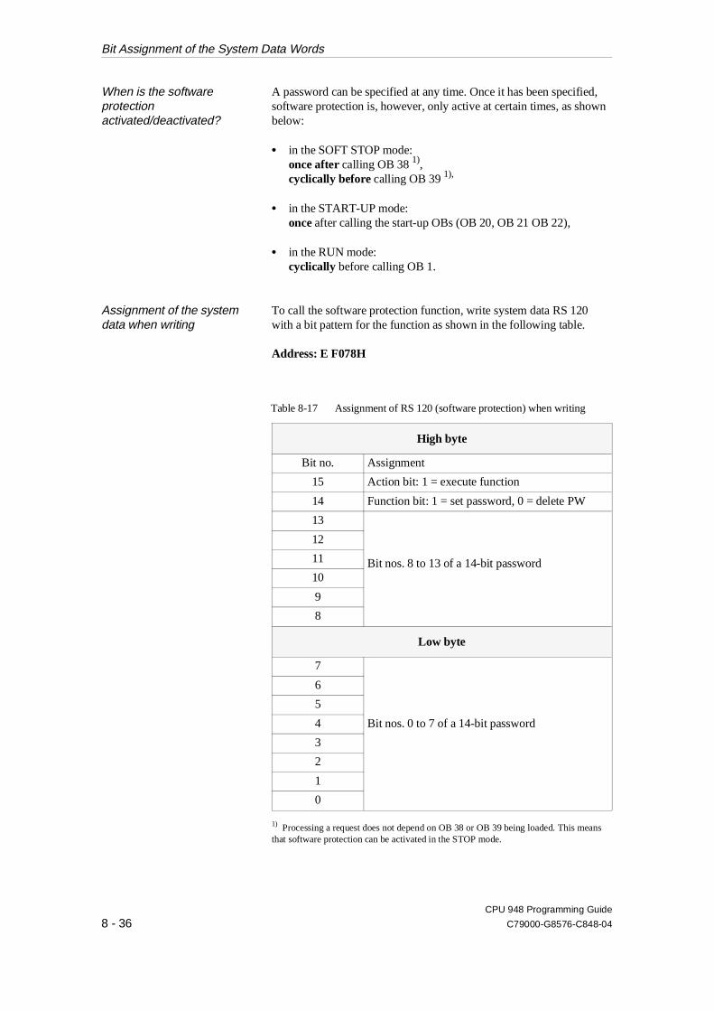
When is the softwareprotectionactivated/deactivated?
A password can be specified at any time. Once it has been specified,software protection is, however, only active at certain times, as shownbelow:
•• in the SOFT STOP mode:once after calling OB 38 1),cyclically before calling OB 39 1),
•• in the START-UP mode:once after calling the start-up OBs (OB 20, OB 21 OB 22),
•• in the RUN mode:cyclically before calling OB 1.
Assignment of the systemdata when writing
To call the software protection function, write system data RS 120with a bit pattern for the function as shown in the following table.
Address: E F078H
High byte
Bit no. Assignment
15 Action bit: 1 = execute function
14 Function bit: 1 = set password, 0 = delete PW
13
Bit nos. 8 to 13 of a 14-bit password
12
11
10
9
8
Low byte
7
Bit nos. 0 to 7 of a 14-bit password
6
5
4
3
2
1
0
1) Processing a request does not depend on OB 38 or OB 39 being loaded. This meansthat software protection can be activated in the STOP mode.
Table 8-17 Assignment of RS 120 (software protection) when writing
Bit Assignment of the System Data Words
CPU 948 Programming Guide
8 - 36 C79000-G8576-C848-04
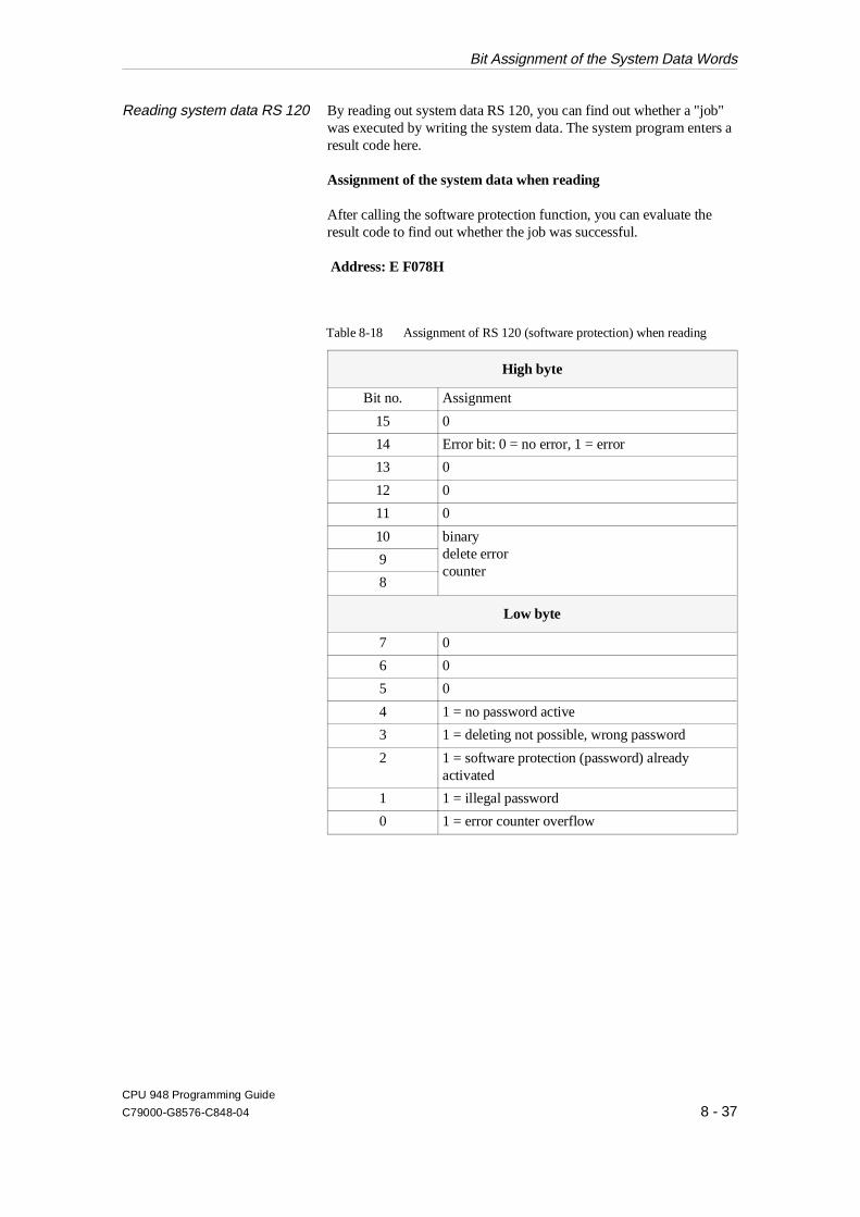
Reading system data RS 120 By reading out system data RS 120, you can find out whether a "job"was executed by writing the system data. The system program enters aresult code here.
Assignment of the system data when reading
After calling the software protection function, you can evaluate theresult code to find out whether the job was successful.
Address: E F078H
High byte
Bit no. Assignment
15 0
14 Error bit: 0 = no error, 1 = error
13 0
12 0
11 0
10 binary delete errorcounter
9
8
Low byte
7 0
6 0
5 0
4 1 = no password active
3 1 = deleting not possible, wrong password
2 1 = software protection (password) alreadyactivated
1 1 = illegal password
0 1 = error counter overflow
Table 8-18 Assignment of RS 120 (software protection) when reading
Bit Assignment of the System Data Words
CPU 948 Programming Guide
C79000-G8576-C848-04 8 - 37
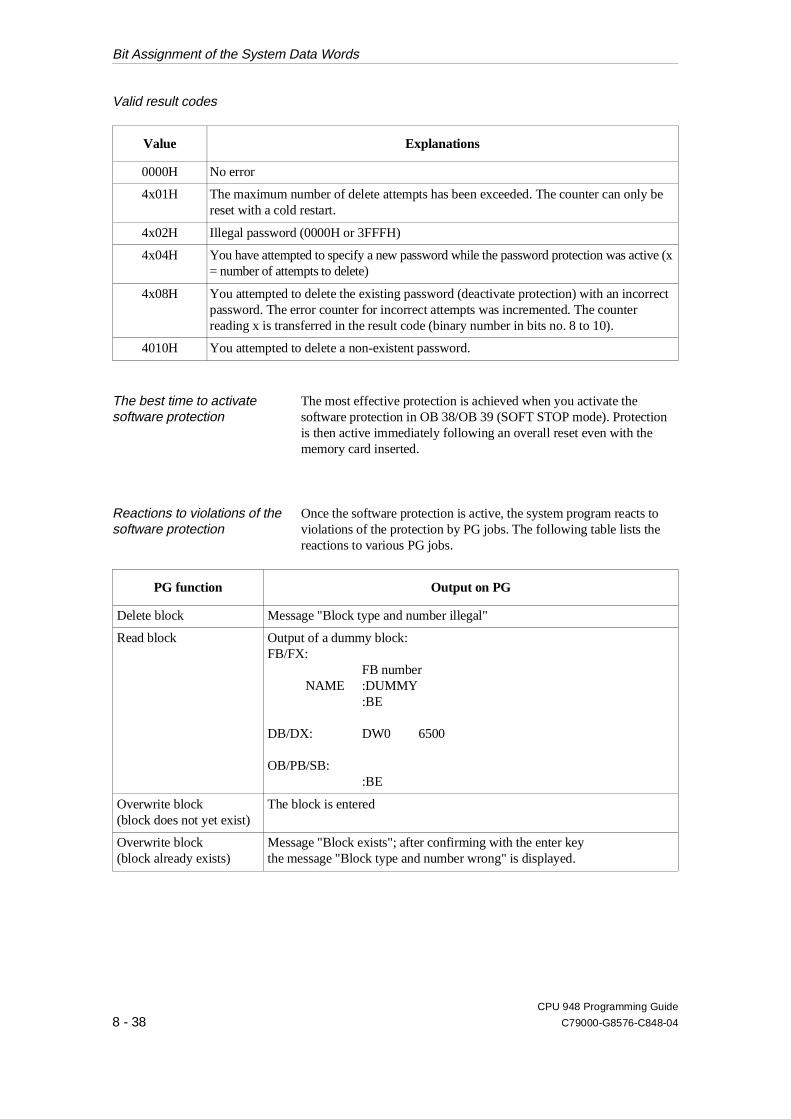
Valid result codes
Value Explanations
0000H No error
4x01H The maximum number of delete attempts has been exceeded. The counter can only bereset with a cold restart.
4x02H Illegal password (0000H or 3FFFH)
4x04H You have attempted to specify a new password while the password protection was active (x= number of attempts to delete)
4x08H You attempted to delete the existing password (deactivate protection) with an incorrectpassword. The error counter for incorrect attempts was incremented. The counterreading x is transferred in the result code (binary number in bits no. 8 to 10).
4010H You attempted to delete a non-existent password.
The best time to activatesoftware protection
The most effective protection is achieved when you activate thesoftware protection in OB 38/OB 39 (SOFT STOP mode). Protectionis then active immediately following an overall reset even with thememory card inserted.
Reactions to violations of thesoftware protection
Once the software protection is active, the system program reacts toviolations of the protection by PG jobs. The following table lists thereactions to various PG jobs.
PG function Output on PG
Delete block Message "Block type and number illegal"
Read block Output of a dummy block:FB/FX:
FB numberNAME :DUMMY
:BE
DB/DX: DW0 6500
OB/PB/SB::BE
Overwrite block(block does not yet exist)
The block is entered
Overwrite block(block already exists)
Message "Block exists"; after confirming with the enter keythe message "Block type and number wrong" is displayed.
Bit Assignment of the System Data Words
CPU 948 Programming Guide
8 - 38 C79000-G8576-C848-04
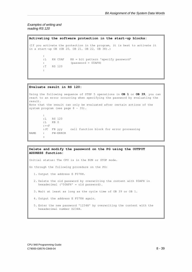
Examples of writing andreading RS 120
Activating the software protection in the start-up blocks:
(If you activate the protection in the program, it is best to activate itin a start-up OB (OB 20, OB 21, OB 22, OB 38).)
::L KH C0AF KH = bit pattern "specify password": (password = 00AFH) :T RS 120:
Evaluate result in RS 120:
Using the following sequence of STEP 5 operations in OB 1 or OB 39 , you canreact to an error occurring when specifying the password by evaluating theresult.Note that the result can only be evaluated after certain actions of thesystem program (see page 8 - 35).
::L RS 120:L KB 0:><F :JC FB yyy call function block for error processing
NAME : PW-ERROR:
Delete and modify the password on the PG using the OUTPUTADDRESS function:
Initial status: The CPU is in the RUN or STOP mode.
Go through the following procedure on the PG:
1. Output the address E F078H.
2. Delete the old password by overwriting the content with 80AFH inhexadecimal ("00AFH" = old password).
3. Wait at least as long as the cycle time of OB 39 or OB 1.
4. Output the address E F078H again.
5. Enter the new password "1234H" by overwriting the content with thehexadecimal number D234H.
Bit Assignment of the System Data Words
CPU 948 Programming Guide
C79000-G8576-C848-04 8 - 39

System data words RS 136 to RS 137
For self-test function
The system data words RS 136 to RS 137 are used for the self-test.
RS 136 Number of time slices (address: E F088H)
RS 137 Control bits (address: E F089H)
Using the control bits, the individual self-test functions can beincluded or excluded (refer to Section 5.7).Bit = ’1’: self-test function is includedBit = ’0’: self-test function is excluded
High byte
Bit no. Assignment
15 Memory test
14 Not used
13 Test cycle time monitoring
12 Not used
11 Test BASP signal
10 Clock test
9 Not used
8 Not used
Low byte
7 Test address lines
6 Not used
5 Code test of the STEP 5 logic blocks inthe user memory
4 Not used
3 Not used
2 Code test of the system program
1 Not used
0 Not used
Table 8-19 Bits of RS 137 (control bits for self-test functions)
Bit Assignment of the System Data Words
CPU 948 Programming Guide
8 - 40 C79000-G8576-C848-04
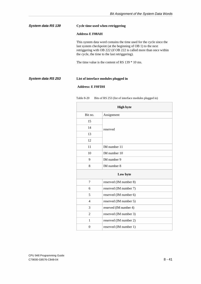
System data RS 139 Cycle time used when retriggering
Address E F08AH
This system data word contains the time used for the cycle since thelast system checkpoint (at the beginning of OB 1) to the nextretriggering with OB 222 (if OB 222 is called more than once withinthe cycle, the time to the last retriggering).
The time value is the content of RS 139 * 10 ms.
System data RS 253 List of interface modules plugged in
Address: E F0FDH
High byte
Bit no. Assignment
15
reserved14
13
12
11 IM number 11
10 IM number 10
9 IM number 9
8 IM number 8
Low byte
7 reserved (IM number 8)
6 reserved (IM number 7)
5 reserved (IM number 6)
4 reserved (IM number 5)
3 reserved (IM number 4)
2 reserved (IM number 3)
1 reserved (IM number 2)
0 reserved (IM number 1)
Table 8-20 Bits of RS 253 (list of interface modules plugged in)
Bit Assignment of the System Data Words
CPU 948 Programming Guide
C79000-G8576-C848-04 8 - 41
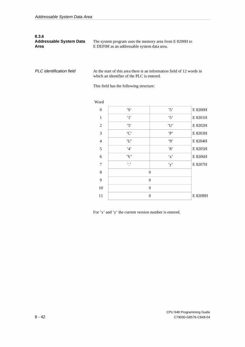
8.3.6Addressable System DataArea
The system program uses the memory area from E 8200H to E DEF0H as an addressable system data area.
PLC identification field At the start of this area there is an information field of 12 words inwhich an identifier of the PLC is entered.
This field has the following structure:
Word
0 ’S’ ’5’ E 8200H
1 ’1’ ’5’ E 8201H
2 ’5’ ’U’ E 8202H
3 ’C’ ’P’ E 8203H
4 ’U’ ’9’ E 8204H
5 ’4’ ’8’ E 8205H
6 ’V’ ’x’ E 8206H
7 ’.’ ’y’ E 8207H
8 0
9 0
10 0
11 0 E 820BH
For ’x’ and ’y’ the current version number is entered.
Addressable System Data Area
CPU 948 Programming Guide
8 - 42 C79000-G8576-C848-04

System parameters System parameters in the memory area beginning with the address E 8210H:
Word
0 Start add. interface module input E 8210H
1 Start add. interface module output E 8211H
2 Start add. process image input table E 8212H
3 Start add. process image output table E 8213H
4 Start add. flags E 8214H
5 Start add. timers E 8215H
6 Start add. counters E 8216H
7 Start add. system data E 8217H
8 Status ID PLC software version E 8218H
9 User memory end address E 8219H
10 System program memory E 821AH
11 Length of DB list E 821BH
12 Length of SB list E 821CH
13 Length of PB list E 821DH
14 Length of FB list E 821EH
15 Length of OB list E 821FH
16 Length of FX list E 8220H
17 Length of DX list E 8221H
18 Length of DB address list (DB 0) E 8222H
19 Slot ID (see below) CPU ID 2 (see below) E 8223H
20 Block header length E 8224H
21 CPU ID 1 (see below) Programmer interfacesoftware version
E 8225H
You can also use the SYSTEM PARAMETER PG online function tofind the information contained in a few system data registers (e.g.,concerning the internal structure of the CPU, the software version, theCPU ID).
Addressable System Data Area
CPU 948 Programming Guide
C79000-G8576-C848-04 8 - 43

Word 19 and word 21 Structure of words 19 and 21:
Word 19
Bit no. High byte
15 0
14 0
13 0
12 0
11 Slot ID CPU 4
10 Slot ID CPU 3
9 Slot ID CPU 2
8 Slot ID CPU 1
Low byte
7 CPU type:0010 = CPU 948(only valid in conjunction with the CPU ID)
6
5
4
3 CPU-ID 2:1000 = S5-155U
2
1
0
Addressable System Data Area
CPU 948 Programming Guide
8 - 44 C79000-G8576-C848-04

Word 21
Bit no. High byte
15 reserved
14
13
12
11
10
9
8
Bit no. Low byte
7
Release of the PG interface softwarein the form "xyH"
Example:13H corresponds to release "V1.3"
6
5
4
3
2
1
0
Addressable System Data Area
CPU 948 Programming Guide
C79000-G8576-C848-04 8 - 45

Addressable System Data Area
CPU 948 Programming Guide
8 - 46 C79000-G8576-C848-04
Contents of Chapter 9
9.1 Introduction. . . . . . . . . . . . . . . . . . . . . . . . . . . . . . . . . . . . . . . . . . . . . . . . . . . . . . . . . . . . . 9 - 4
9.2 Memory Access via Addresses in ACCU 1 . . . . . . . . . . . . . . . . . . . . . . . . . . . . . . . . . . . . 9 - 8
9.2.1 LIR/TIR: Loading to or Transferring from a 16-Bit Memory Area Indirectly. . . . . . . . . 9 - 99.2.2 Examples of Access to DW > 255 . . . . . . . . . . . . . . . . . . . . . . . . . . . . . . . . . . . . . . . . . 9 - 159.2.3 LDI/TDI: Loading to or Transferring from a 32-Bit Memory Area Indirectly . . . . . . . 9 - 17
9.3 Transferring Memory Blocks . . . . . . . . . . . . . . . . . . . . . . . . . . . . . . . . . . . . . . . . . . . . . . 9 - 19
9.4 Operations with the Base Address Register (BR Register). . . . . . . . . . . . . . . . . . . . . . . 9 - 22
9.4.1 Operations for Transfer between Registers . . . . . . . . . . . . . . . . . . . . . . . . . . . . . . . . . . . 9 - 239.4.2 Accessing the Local Memory. . . . . . . . . . . . . . . . . . . . . . . . . . . . . . . . . . . . . . . . . . . . . . 9 - 249.4.3 Accessing the Global Memory. . . . . . . . . . . . . . . . . . . . . . . . . . . . . . . . . . . . . . . . . . . . . 9 - 259.4.4 Accessing the Dual-Port RAM Memory . . . . . . . . . . . . . . . . . . . . . . . . . . . . . . . . . . . . . 9 - 29
9Memory Access UsingAbsolute Addresses
CPU 948 Programming Guide
C79000-G8576-C848-04 9 - 1

Contents
CPU 948 Programming Guide
9 - 2 C79000-G8576-C848-04
9Memory Access Using Absolute Addresses
This chapter explains how to use STEP 5 operations and specialSTEP 5 registers to address data in certain memory areas usingabsolute addresses.
CPU 948 Programming Guide
C79000-G8576-C848-04 9 - 3

9.1 Introduction
The STEP 5 programming language contains operations with whichyou can access the entire memory area. These operations belong to the"system operations".
The operations described in this chapter work with 20-bit absoluteaddresses. Consequently, they are dependent on the memory size andtype, the peripherals, CPs, and IPs of your programmable controller.
WarningIf the operations described in this chapter are not used properly,STEP 5 blocks and system data can be overwritten. Therefore,only experienced programmers should use operations that workwith absolute addresses.
Local memory Local memory is the memory area that is available in each CPU. Itincludes the following: user submodule, RI/RJ area, RS/RT area,counters, timers, flags, process images.
Global memory Global memory exists only once for all CPUs. You address it via theS5 bus.
Memory organization Memory areas are organized in bytes or in words as follows:
•• Bytes: Each address addresses a byte.
•• Words: Each address addresses a 16-bit word(= 2 bytes).
Organization of the local memory is fixed (see Chapter 8)
Organization of the global memory depends on the type of modulesthat are plugged into the programmable controller:
Introduction
CPU 948 Programming Guide
9 - 4 C79000-G8576-C848-04
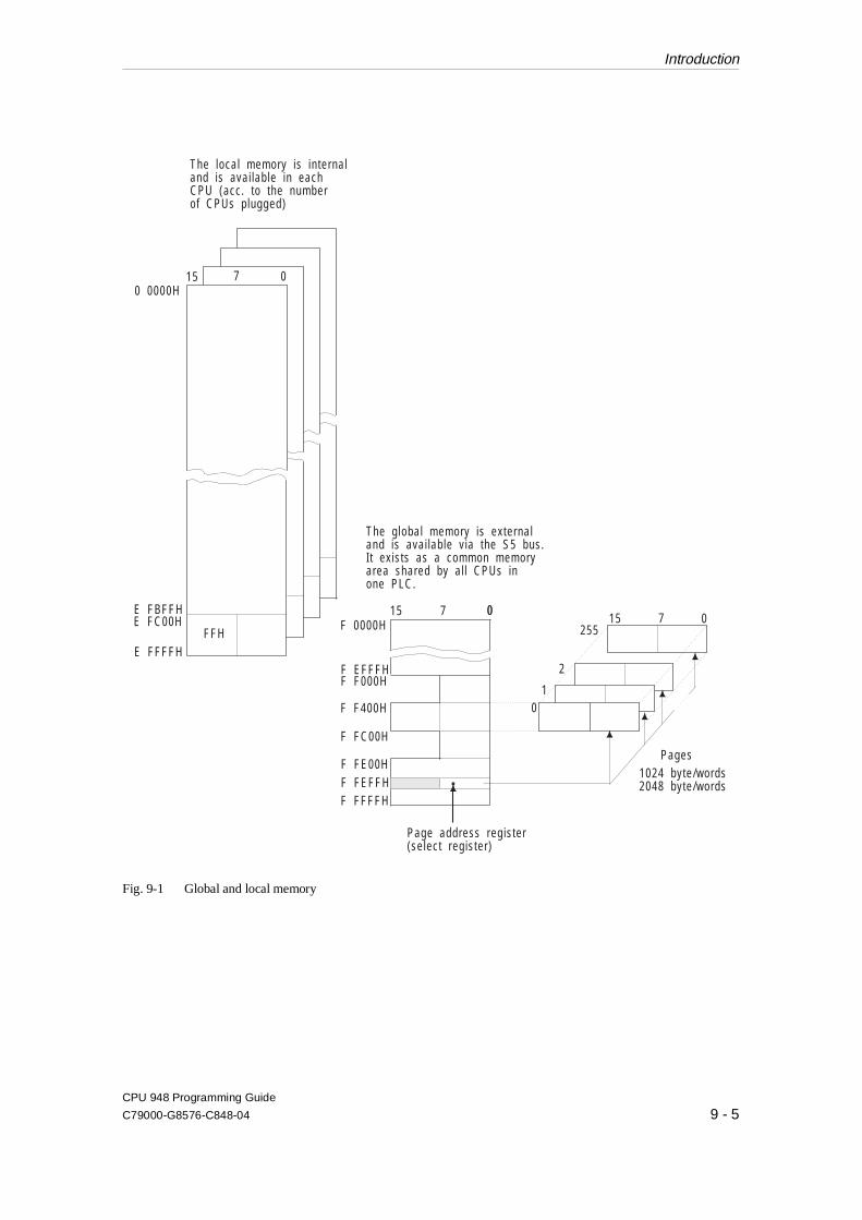
015
Pages
7
1024 byte/words2048 byte/words
F 0000H
F F000H
F F400H
F FC00H
F FE00H
F FFFFHF FEFFH
F EFFFH
Page address register(select register)
The global memory is externaland is avai lable via the S5 bus.I t exists as a common memoryarea shared by al l CPUs inone PLC.
The local memory is internaland is avai lable in eachCPU (acc. to the numberof CPUs plugged)
715 00 0000H
E FBFFHE FC00H
E FFFFHFFH
0715 0
255
2
10
Fig. 9-1 Global and local memory
Introduction
CPU 948 Programming Guide
C79000-G8576-C848-04 9 - 5
Memory access Using absolute addresses, you can access the following local or globalmemory areas with the operations indicated (refer to Fig. 9-2).
Access to the local and globalarea
You can access both the local and global areas:
•• Local area (addresses 0 0000H to E FFFFH) and global area(addresses F 0000H to F FFFFH) with:
LIR, TIR, LDI, TDI, TNW, TXB, TXW,
•• Section of the local area organized in words (addresses 0 0000Hto E FBFFH) or in bytes (addresses E FC000 to E FFFF) with:
LRW, TRW, LRD, TRD.
Access only to the global area You can access the following parts of the global area:
•• Section of the global area organized in bytes (addresses F 0000Hto F FFFFH) with:
LY GB, LY GW, LY GD, TY GB, TY GW, TY GD, TSG,
•• Section of the global area organized in words (addresses F 0000Hto F FFFFH) with:
LW GW, LW GD, TW GW, TW GD, TSG .
Access to the page area You can access the following parts of the page area:
•• Section of the global area organized in bytes (addresses F F400Hto F FBFFH, = dual-port RAM area) with:
LY CB, LY CW, LY CD, TY CB, TY CW, TY CD, TSC,
•• Section of the global area organized in words (addresses F F400Hto F FBFFH, = dual-port RAM area) with:
LW CW, LW CD, TW CW, TW CD, TSC
Introduction
CPU 948 Programming Guide
9 - 6 C79000-G8576-C848-04
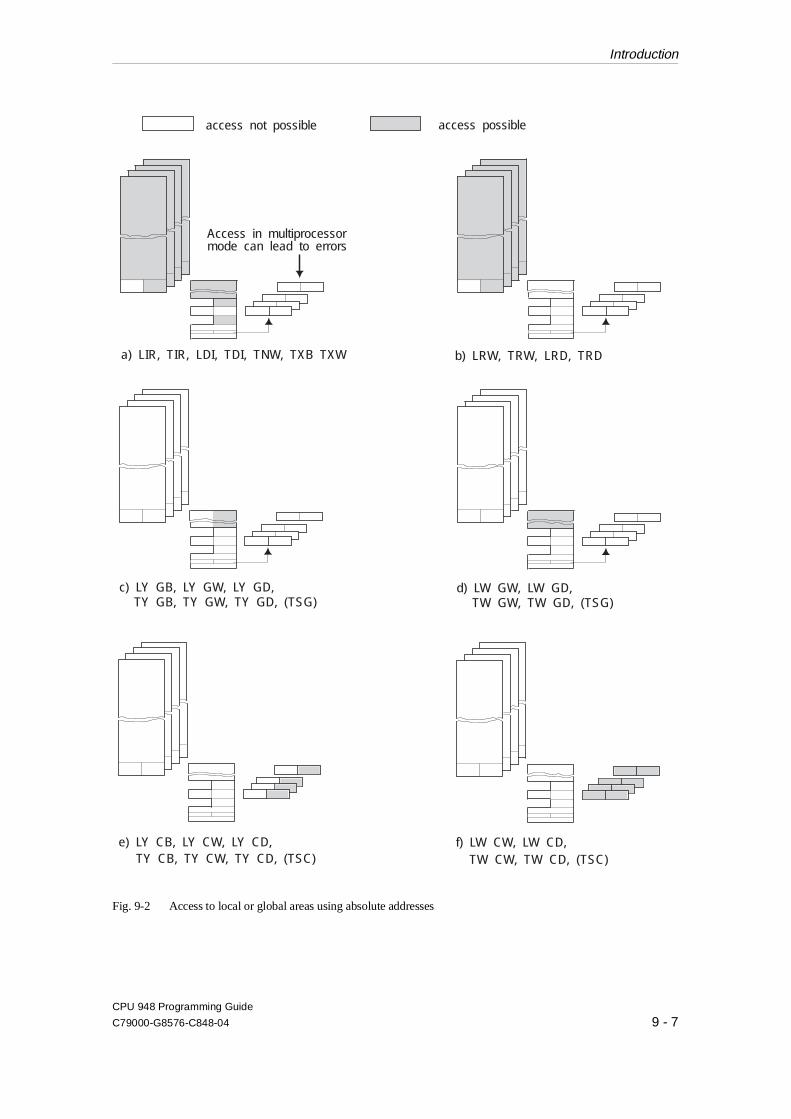
access not possible access possible
c) LY GB, LY GW, LY GD,
e) LY CB, LY CW, LY CD,TY CB, TY CW, TY CD, (TSC)
f) LW CW, LW CD,TW CW, TW CD, (TSC)
TY GB, TY GW, TY GD, (TSG)d) LW GW, LW GD,
TW GW, TW GD, (TSG)
b) LRW, TRW, LRD, TRDa) LIR, TIR, LDI, TDI, TNW, TXB TXW
Access in multiprocessormode can lead to errors
Fig. 9-2 Access to local or global areas using absolute addresses
Introduction
CPU 948 Programming Guide
C79000-G8576-C848-04 9 - 7
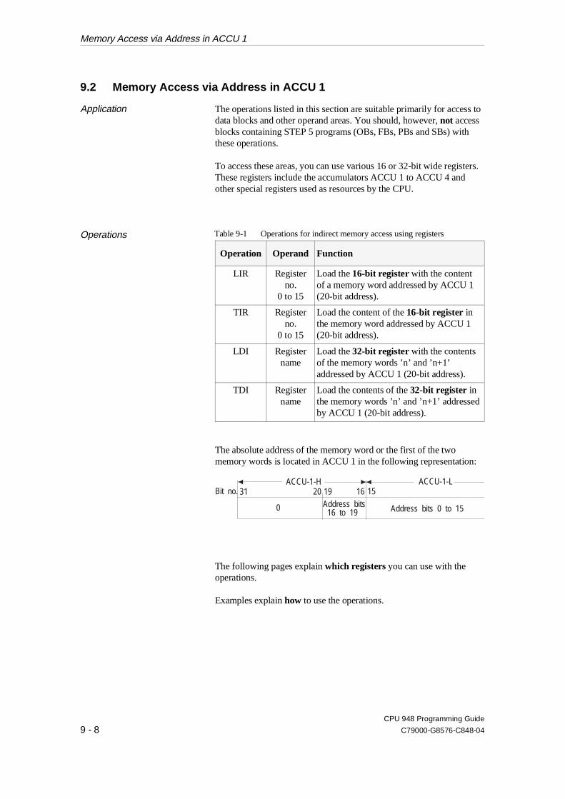
9.2 Memory Access via Address in ACCU 1
Application The operations listed in this section are suitable primarily for access todata blocks and other operand areas. You should, however, not accessblocks containing STEP 5 programs (OBs, FBs, PBs and SBs) withthese operations.
To access these areas, you can use various 16 or 32-bit wide registers.These registers include the accumulators ACCU 1 to ACCU 4 andother special registers used as resources by the CPU.
Operations
Operation Operand Function
LIR Registerno.
0 to 15
Load the 16-bit register with the contentof a memory word addressed by ACCU 1(20-bit address).
TIR Registerno.
0 to 15
Load the content of the 16-bit register inthe memory word addressed by ACCU 1(20-bit address).
LDI Registername
Load the 32-bit register with the contentsof the memory words ’n’ and ’n+1’addressed by ACCU 1 (20-bit address).
TDI Registername
Load the contents of the 32-bit register inthe memory words ’n’ and ’n+1’ addressedby ACCU 1 (20-bit address).
The absolute address of the memory word or the first of the twomemory words is located in ACCU 1 in the following representation:
The following pages explain which registers you can use with theoperations.
Examples explain how to use the operations.
Table 9-1 Operations for indirect memory access using registers
Bit no.ACCU-1-H ACCU-1-L
31 20 19 16 15
0 Address bits Address bits 0 to 1516 to 19
Memory Access via Address in ACCU 1
CPU 948 Programming Guide
9 - 8 C79000-G8576-C848-04

9.2.1LIR/TIR: Loading to or Transferring from a 16-BitMemory Area Indirectly
The following table shows which register numbers you can use withthe CPU 948 for the LIR and TIR operations and how these areassigned.
Register no. Register assignment (each 16 bits wide)
0 ACCU-1-H (left word of ACCU1, bits 16 to 31)1)
1 ACCU-1-L (right word of ACCU1, bits 0 to 15)1)
2 ACCU-2-H
3 ACCU-2-L
5 Block stack pointer (offset)
6 DBA (data block start address register)
8 DBL (data block length register)
9 ACCU-3-H
10 ACCU-3-L
11 ACCU-4-H
12 ACCU-4-L
1) Loading the contents of an addressed memory register into register ’0’or ’1 overwrites the address stored in ACCU 1.
Registers 4, 7, 13, 14 and 15 do not exist on the CPU 948. LIR/TIRoperations with these register numbers must not be used.
LIR/TIR: with 8-bitmemory areas
If you use the LIR and TIR operations to access memory areas that areonly 8 bits wide, remember that
•• the LIR operation overwrites the high byte of the registers withnon-defined values (except for flags, PIQ, PII; with these areas,FFH is written in the high byte)
and
•• the TIR operation transfers only the low byte of the register. Thehigh byte of the register is lost.
Figs. 9-3 and 9-4 illustrate the difference when accessing word andbyte-oriented memory areas using LIR/TIR.
Table 9-2 16-bit register for LIR/TIR
Memory Access via Address in ACCU 1
CPU 948 Programming Guide
C79000-G8576-C848-04 9 - 9

19 0 15 0
19 0
ACCU 1
ACCU 1
Register n
Register n
addressedmemorylocat ion
addressedmemorylocat ion
15 0
LIR n
TIR n
15 0
Fig. 9-3 LIR/TIR with 16-bit memory areas (word-oriented)
19 0 15 0
19 0
ACCU 1
ACCU 1
Register n
Register n
addressedmemorylocat ion
addressedmemorylocat ion
15 0
LIR n
x x
x x
TIR n
7 0
Fig. 9-4 LIR/TIR with 8-bit memory areas (byte-oriented)
Memory Access via Address in ACCU 1
CPU 948 Programming Guide
9 - 10 C79000-G8576-C848-04
Registers 0 to 3 and 9 to 12:ACCUs 1, 2, 3 and 4
During program processing, the accumulators are used as buffers forthe CPU. The TIR operation transfers the contents of the accumulatorsinto absolutely addressed memory registers. The LIR operation loadsthe contents of absolutely addressed memory registers into theaccumulators. The absolute address of the memory locations is inACCU 1, bit number 0 to 19.
Examples
Register 6: DBA (Data BlockStart Address)
When you open a data block or an extended data block using the C DB or CX DX operations, the address of DW 0 in the opened datablock is loaded into register 6. The block address list in DB 0 containsthis address.The DBA register is set to ’0’ before each OB 1 call.
The DBA register remains the same if one of the following occurs:
•• a jump operation (JU/JC) causes program processing to continue ina different block,
or
•• the CPU activates a different program processing level.
The contents of the memory location with address E F800 are loaded in flagword FW 100.
:L DH 000E F800 Load address E F800 of the memory location in ACCU 1:LIR 1 Load the contents of the memory location addressed by: ACCU 1 in register 1 (= ACCU-1-L):T FW 100 Store the contents of address E F800 in flag word FW 100:BE
The content of the flag word 200 is transferred to the memory location withaddress E F800.
:L FW 200 Load flag word FW 200 in ACCU 1:L DH 000E F800 Load address E F800 to which the data will be trans-: ferred in ACCU 1 (flag word FW 200 to ACCU 2):TIR 3 Transfer the contents of register 3 = ACCU-2-L in to : the memory location addressed by ACCU 1:BE
Memory Access via Address in ACCU 1
CPU 948 Programming Guide
C79000-G8576-C848-04 9 - 11
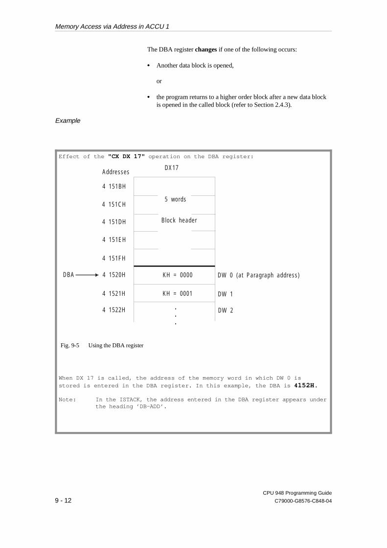
The DBA register changes if one of the following occurs:
•• Another data block is opened,
or
•• the program returns to a higher order block after a new data blockis opened in the called block (refer to Section 2.4.3).
Example
Effect of the "CX DX 17" operation on the DBA register:
When DX 17 is called, the address of the memory word in which DW 0 isstored is entered in the DBA register. In this example, the DBA is 4152H.
Note: In the ISTACK, the address entered in the DBA register appears underthe heading ’DB-ADD’.
5 words
Block header
KH = 0000
KH = 0001
4 151BH
4 151CH
4 151DH
4 151EH
4 151FH
4 1520H
4 1521H
4 1522H
DW 0 (at Paragraph address)
DW 1
DW 2
DBA
AddressesDX17
.
.
.
Fig. 9-5 Using the DBA register
Memory Access via Address in ACCU 1
CPU 948 Programming Guide
9 - 12 C79000-G8576-C848-04

Register 8: DBL = Data Block Length
In addition to the DBA register, a DBL register is loaded every time adata block is called. It contains the length (in words) of the data blockcalled, without the block header. The DBL register is set to ’0’ beforeeach OB 1 call.
DBL register is retained, when
•• program execution is continued in a different block following ajump statement (JU/JC)
or
•• a different program execution level is nested in.
It changes when
•• a different data block is opened
or
•• program execution returns to a higher order block after a new datablock is opened in the called block (refer to Section 2.4.2).
NoteYou can change the DBA and DBL registers using LIR operationsto address data block addresses higher than 255. The DBAregister contains paragraph addresses. Make sure that a changein the DBA register does not automatically cause a change in theDBL register and vice-versa. This would mean that transfererror monitoring is no longer guaranteed.On the CPU 948, changes in the DBA/DBL registers are undone,as soon as the current block is completed (BSTACK entries).Manipulations on the DBA/DBL registers are therefore onlyeffective in the block in which they were made.
Memory Access via Address in ACCU 1
CPU 948 Programming Guide
C79000-G8576-C848-04 9 - 13
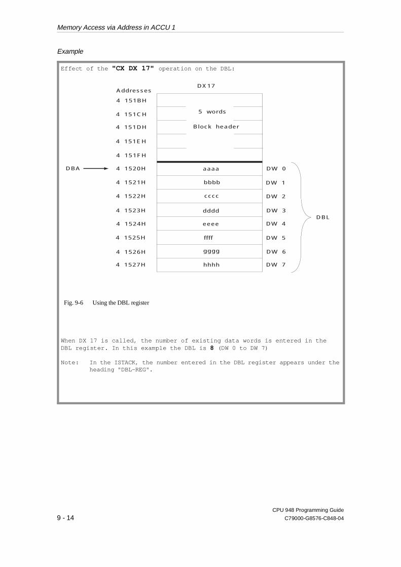
Example
Effect of the "CX DX 17" operation on the DBL:
When DX 17 is called, the number of existing data words is entered in theDBL register. In this example the DBL is 8 (DW 0 to DW 7)
Note: In the ISTACK, the number entered in the DBL register appears under theheading "DBL-REG".
5 words
Block header
eeee
ffff
gggg
aaaa
bbbb
cccc
dddd
hhhh
4 151BH
4 151CH
4 151DH
4 151EH
4 151FH
4 1520H
4 1521H
4 1522H
4 1523H
4 1524H
4 1525H
4 1526H
4 1527H
DW 0
DW 1
DW 2
DW 3
DW 4
DW 5
DW 6
DW 7
DBA
DBL
AddressesDX17
Fig. 9-6 Using the DBL register
Memory Access via Address in ACCU 1
CPU 948 Programming Guide
9 - 14 C79000-G8576-C848-04
9.2.2Examples of Access toDW > 255
Example 1:
The content of data word DW 300 in DB 100 is read and transferred to flagword FW 100 (by changing the STEP 5 operation shown in bold face, it canalso be used to read other data blocks (DB or DX)).
FB 5
SEGMENT 1 0000 Reading out DW 300 from DB 100NAME :LIR DW
0005 :L DH 000E EC00 Start addr. of the DB list0008 :L KF +100 plus the DB number000A :+D = Address list entry of DB 100000B : (Bits 4 to 19)000C :LIR 1 Start addr. DB 100 to ACCU 1000D :SLD 4 Convert addr. to physical addr.000E :L KF +300 DW 300 is read out0010 :+D Addr. = start addr. of DB + DW addr.0011 :LIR 1 Store content of DW 300 to ACCU 10012 :T FW 100 in FW 1000013 :BE
Example 2:
All the data words of a data block will have a constant written to them.
The program shown below writes the constant KH = A5A5 to all data words ofDB 100. After changing the STEP 5 operations shown in bold face, it canalso be used to write values to other data blocks (DB or DX). Non-existentdata blocks are detected and cause a jump to the NIVO marker.
The program uses three accumulators. Within the loop, the accumulatorcontents do not change.ACCU 1 initially contains the address of the first data word and isincremented by one each time the loop is run through.ACCU 2 contains the address of the last data word + 1. The loop isterminated as soon as the content of ACCU 1 is the same as the content ofACCU 2.
To write the data words, the operation TIR 10 is used which stores thecontent of ACCU-3-L (the constant) at the address contained in ACCU 1.
ACCU contents within the loop:
ACCU 1: address of the current data word to be written toACCU 2: address of the last data word to be written to + 1ACCU 3: constant
Continued on the next page
Memory Access via Address in ACCU 1
CPU 948 Programming Guide
C79000-G8576-C848-04 9 - 15

Example 2 continued:
Flag assignment:
FW 10: Bits 4 to 19 of the start address of the DB/DX (points to DW 0)FW 12: Length of the DB/DX (number of data words)FD 14: Address of the last data word in the DB/DX + 1 (physical address)
FB 6
SEGMENT 1 0000 Writing a DB with a constantNAME :FILL DB0005 : ! Required flags: FY 10 to FY 17 !
0006 :L DH 000E EC00 Start addr. of the DB list0009 :L KF +100 plus the DB number000B :+D = Address list entry of DB 100000C : (Bits 4 to 19)000D :LIR 1 Start addr. DB 100 to ACCU 1000E :T FW 10 Buffer start addr.000F :L KB 0 (Paragraph address)0010 :!=F If start addr. = 0, then0011 :JC =NIVO DB does not exist0012 :0013 :L FW 10 Start addr. of DB (1st DW)0014 :SLD 4 Convert addr. to physical address0015 :L KB 1 Find out DB length via0016 :-D 5th word in block header0017 :LIR 1 Length including block header to ACCU 10018 :ADD BN -5 Number of DWs = total length - 5 words (header)0019 :001A :T FW 12 Buffer length001B :001C :L FW 12 Number of data words +001D :L FW 10 start address (DW 0 converted to001E :SLD 4 physical address) 001F :+D produces0020 :T FD 14 address of the last DW + 10021 :
0022 :L KH A5A5 Constant, written to all data words0024 : 0025 :L FD 14 Address of the last DW + 10026 :ENT Shift constant to ACCU-3-L0027 : (= register 10)0028 :L FW 10 Convert address of 1st data word (DW 0)0029 :SLD 4 to physical address002A :002B SCHL : Loop:002C : ACCU 1: address of DW to be written to002D : ACCU 2: address of last DW + 1002E : ACCU 3: constant002F :TIR 10 Store the value of ACCU-3-L in the DW with0030 : the address in ACCU 10031 :0032 :ADD DH 0000 0001 Increment address by 10035 :0036 :><D Scan whether last DW reached0037 :JC =SCHL (if not, return to the loop)0038 :0039 WEIT : Continue the program ...003A : after all DWs have been written to ...003B :003C :BEU003D :003E NIVO : If DB 100 does not exist003F :BE
Memory Access via Address in ACCU 1
CPU 948 Programming Guide
9 - 16 C79000-G8576-C848-04

9.2.3LDI/TDI: Loading to orTransferring from a 32-BitMemory Area Indirectly
The following table shows which register names you can use on theCPU 948 for the LDI and TDI operations and how these are assigned.
Register name Register assignment (each 32 bits wide)
A1 ACCU 1 (ACCU1, bits 0 to 31) 1)
A2 ACCU 2 (ACCU1, bits 0 to 31)
SA STEP address counter (bits 0 to 19)
BA BA register (block start address, bits 0 to 19)
BR BR register (base address register, bits 0 to 19)
1) Loading the contents of an addressed memory register into the A1 register overwritesthe address stored in ACCU 1.
Byte addresses If you reference byte addresses with the LDI or TDI operations, notethe following:
•• the LDI operation overwrites the high byte of the register with non-defined values (except for flags, PIQ, PII; with these areas, FFH iswritten in the high byte)
and
•• the TDI operation transfers only the low bytes of the register (thehigh bytes are lost – refer to the example on the following page
Data storage with LDI/TDI
Table 9-3 32-bit register for LDI/TDI
High register Low register31 16 15
15
DW n
Address
DW n+1
0
0
aaaa
aaaa
bbbb
bbbb
Memory Access via Address in ACCU 1
CPU 948 Programming Guide
C79000-G8576-C848-04 9 - 17
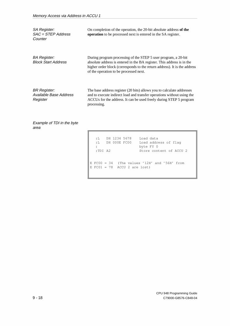
SA Register: SAC = STEP AddressCounter
On completion of the operation, the 20-bit absolute address of theoperation to be processed next is entered in the SA register.
BA Register:Block Start Address
During program processing of the STEP 5 user program, a 20-bitabsolute address is entered in the BA register. This address is in thehigher order block (corresponds to the return address). It is the addressof the operation to be processed next.
BR Register:Available Base AddressRegister
The base address register (20 bits) allows you to calculate addressesand to execute indirect load and transfer operations without using theACCUs for the address. It can be used freely during STEP 5 programprocessing.
Example of TDI in the bytearea
:L DH 1234 5678 Load data:L DH 000E FC00 Load address of flag: byte FY 0:TDI A2 Store content of ACCU 2
E FC00 = 34 (The values ’12H’ and ’56H’ fromE FC01 = 78 ACCU 2 are lost)
Memory Access via Address in ACCU 1
CPU 948 Programming Guide
9 - 18 C79000-G8576-C848-04

9.3 Transferring Memory Blocks
Application With the operations explained in this section, you can re-store dataareas with a length of up to 255 words located in certain address areas.
Operations
Operation Operand Function
TNW 0 to 255 Field transfer 0 to 255 words 1)
(in the 16-bit memory area)
TXB -- Field transfer from 8-bit to the 16-bitmemory
TXW -- Field transfer from the 16-bit to the8-bit memory
1) Can also be used for transfer from the byte to the byte area.
Parameters Field length
For TNW: Operand = number of words (0 to 255)
For TXB/TXW ACCU 3 = number of words (0 to 127)
End address of the source area
ACCU 2 = end address of the source area (20 bits)
End address of the destination area
ACCU 1 = end address of the destination area (20 bits)
The entire source and destination areas must be located in one of thememory areas listed in Table 9-5 and cannot overlap.
Permitted memory areas
Addresses Memory area
0 0000H to C FFFFHUser memory:16-bit area (dependent on memoryconfiguration)
Table 9-4 Operations for field transfer
Table 9-5 Memory areas permitted for TNW, TXB and TXW
Transferring Memory Blocks
CPU 948 Programming Guide
C79000-G8576-C848-04 9 - 19
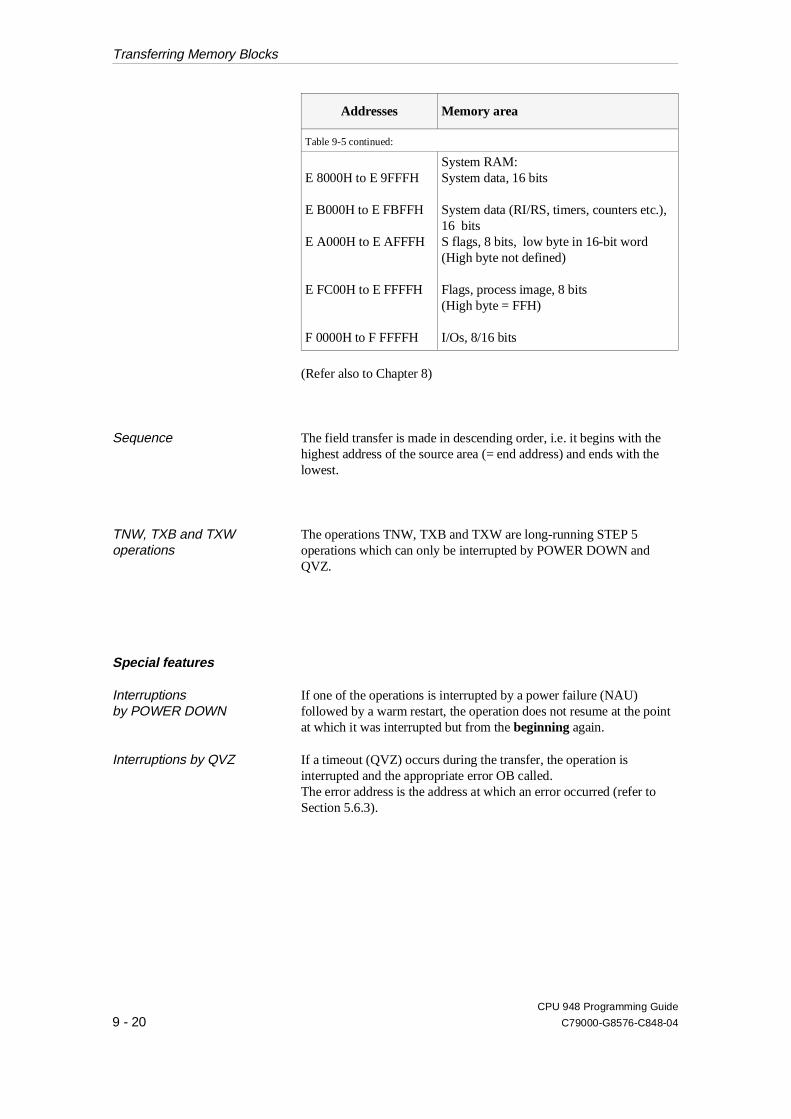
Addresses Memory area
Table 9-5 continued:
E 8000H to E 9FFFH
E B000H to E FBFFH
E A000H to E AFFFH
E FC00H to E FFFFH
F 0000H to F FFFFH
System RAM:System data, 16 bits
System data (RI/RS, timers, counters etc.),16 bitsS flags, 8 bits, low byte in 16-bit word(High byte not defined)
Flags, process image, 8 bits(High byte = FFH)
I/Os, 8/16 bits
(Refer also to Chapter 8)
Sequence The field transfer is made in descending order, i.e. it begins with thehighest address of the source area (= end address) and ends with thelowest.
TNW, TXB and TXW operations
The operations TNW, TXB and TXW are long-running STEP 5operations which can only be interrupted by POWER DOWN andQVZ.
Special features
Interruptionsby POWER DOWN
If one of the operations is interrupted by a power failure (NAU)followed by a warm restart, the operation does not resume at the pointat which it was interrupted but from the beginning again.
Interruptions by QVZ If a timeout (QVZ) occurs during the transfer, the operation isinterrupted and the appropriate error OB called.The error address is the address at which an error occurred (refer toSection 5.6.3).
Transferring Memory Blocks
CPU 948 Programming Guide
9 - 20 C79000-G8576-C848-04

ADF during execution If an addressing error (ADF) occurs once or more than once during thetransfer, all the part fields are first transferred and then OB 25 is calledbefore the next operation is executed.
Example
TXB and TXW between 8 and 16-bit memory areas:
Transferring bytes 1 to 6 from an 8-bit to a 16-bit area:
:L <field length in words> e.g. :L KH 0003:L <source address> :L DH EFC10:ENT :ENT:L <destination address> :L DH EF208:TXB :TXB
Transferring bytes 1 to 6 from a 16-bit to an 8-bit area:
:L <field length in words> e.g. :L KH 0003:L <source address> :L DH EF008:ENT :ENT:L <destination address> :L DH EFC10:TXW :TXW
7 0
AscendingAddresses
Byte 5
Byte 6 TXB
TXW
Byte 4Byte 3Byte 2Byte 1
Source/Dest inat ionAddress
15 7 0
AscendingAddresses
Source/Dest inat ionAddress
Byte 4
Byte 2
Byte 5Byte 6Byte 3Byte 1
8
Fig. 9-7 Transferring memory fields
Transferring Memory Blocks
CPU 948 Programming Guide
C79000-G8576-C848-04 9 - 21
9.4 Operations with the Base Address Register (BR Register)
Application The base address register (20 bits) allows you to calculate addressesand use indirect register load and transfer operations without using theACCUs.The memory location whose absolute address is calculated as the sumof the BR register content plus a constant is accessed.
Absolute address = BR register content + constant
Operations
Operation Operand Function
MBR
ABR
Constant(0H to F FFFFH)
Constant(-32 768 to+32 767)
Load the BR register with a 20-bit constant
Add a 16-bit constant to the contentsof the BR register
Changing the BR register •• The BR register is retained, when the program is continued in adifferent block of the same program execution level due to ajump statement (’JU FB’/’JC FB’).
•• The BR register is retained after nesting in a different programexecution level.
•• If a different program execution level is called by the systemprogram, the BR register is set to ’0’ .
Table 9-6 Load and arithmetic operations with the BR register
Operations with the Base Address Register (BR Register)
CPU 948 Programming Guide
9 - 22 C79000-G8576-C848-04
9.4.1Operations for Transfer between Registers
Application You can use the operations described in this section for the fastexchange of values between the registers ACCU 1 (32 bits), stepaddress counter (SAC - 20 bits) and BR register (20 bits).
Operations
Operation Operand Function
MAS
MAB
MSA
MSB
MBA
MBS
--
--
--
--
--
---
Transfer the contents of ACCU 1 tothe STEP address counter (20 bits)
Transfer the contents of ACCU 1 tothe base address register (20 bits)
Transfer the contents of the STEP address counter (20 bits) to ACCU 1 1)
Transfer the contents of the STEPaddress counter (20 bits) to the baseaddress register (20 bits)
Transfer the contents of the baseaddress register (20 bits) to ACCU 1 1)
Transfer the contents of the baseaddress register (20 bits) to the STEPaddress counter (20 bits)
1) Bits 220 to 231 are set to ’0’.
The following figure illustrates how the registers are changed by theoperations.
Table 9-7 Register-register operations
Operations with the Base Address Register (BR Register)
CPU 948 Programming Guide
C79000-G8576-C848-04 9 - 23
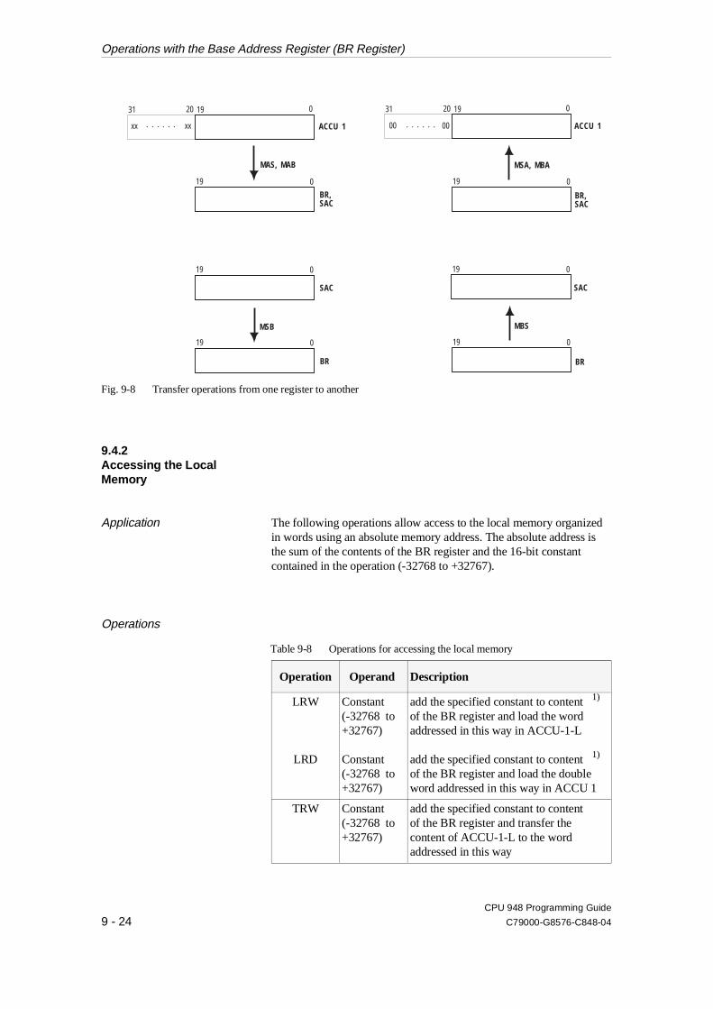
9.4.2Accessing the Local Memory
Application The following operations allow access to the local memory organizedin words using an absolute memory address. The absolute address isthe sum of the contents of the BR register and the 16-bit constantcontained in the operation (-32768 to +32767).
Operations
Operation Operand Description
LRW
LRD
Constant(-32768 to+32767)
Constant(-32768 to+32767)
add the specified constant to content 1)
of the BR register and load the wordaddressed in this way in ACCU-1-L
add the specified constant to content 1)
of the BR register and load the doubleword addressed in this way in ACCU 1
TRW Constant(-32768 to+32767)
add the specified constant to contentof the BR register and transfer thecontent of ACCU-1-L to the wordaddressed in this way
31
xx 00 00. . . . . . . . . . . .xx
20 19 0
ACCU 1
MAS, MAB MSA, MBA
BR,SAC
BR,SAC
ACCU 1
31 20 19 0
19 0 19 0
MSB MBS
SAC
BR BR
SAC
19 0
19 0 19 0
19 0
Fig. 9-8 Transfer operations from one register to another
Table 9-8 Operations for accessing the local memory
Operations with the Base Address Register (BR Register)
CPU 948 Programming Guide
9 - 24 C79000-G8576-C848-04
Operation Operand Description
Table 9-8 continued:
TRD Constant(-32768 to+32767)
add the specified constant to contentof the BR register and transfer thecontent of ACCU 1 to the double wordaddressed in this way
1) ACCU 2 new = ACCU 1old
Error reaction If the calculated address of the memory location is not between0 0000H and E FFFFH, the CPU detects a load/transfer error (TRAF)and calls OB 32. If OB 32 is not loaded, the CPU changes to the stopmode with the error code TRAF (ISTACK).
9.4.3Accessing the GlobalMemory
Application This section describes the operations you can use with absolutememory addresses to access the global memory organized in bytes orwords. The absolute address is the sum of the contents of the BRregister and the constants contained in the operation (-32768 to 32767).
Testing and setting an"occupied" register in the global area
You can control access of individual CPUs to commonly used memoryareas by using an "occupied" register. An "occupied" register is assignedto each commonly used memory area. Each participating CPU must testthis register before accessing the memory area. The "occupied" registercontains either the value ’0’ or the slot ID of the CPU that is presentlyusing the memory area. When the CPU is finished using the memoryarea, it writes ’0’ to the "occupied" register to re-enable the memoryarea. (Note the explanations for the operations "set semaphore/SED" and"enable semaphore/SEE" in Section 3.5.5.)
The TSG operation enables testing and setting of "occupied" registers.
Operation Operand Description
TSG -32768 to+32767
Add the specified constant to the contentof the BR register and test and set thelocation addressed in this way.
Operations with the Base Address Register (BR Register)
CPU 948 Programming Guide
C79000-G8576-C848-04 9 - 25

Sequence The location used is the low byte of the word addressed by the BRregister plus the constant. If the content of the low byte is ’0’, the TSGoperation enters the slot ID in the location.
Testing (reading) and possible occupation of the location (writing)form a program unit that cannot be interrupted.
Result You can evaluate the result of the test using condition codes CC 0 andCC 1:
CC 1 CC 0 Description
0
1
0
0
0
1
The "occupied" register contains ’0’. The CPUenters its own slot ID.
The slot ID of the CPU is already enteredin the "occupied" register.
The "occupied" register contains adifferent slot ID.
NoteAll CPUs that require synchronized access to a common globalmemory area must use the TSG operation.
Error reaction The absolute address must be between F 0000H and F FFFFH. If theabsolute addresses are not in the range shown, the CPU detects atransfer error (TRAF) and calls OB 32. If OB 32 is not loaded, theCPU changes to the STOP mode with the error code TRAF (ISTACK).
Operations with the Base Address Register (BR Register)
CPU 948 Programming Guide
9 - 26 C79000-G8576-C848-04
Load and transferoperations on the global memory organized in bytes
Operation Operand Description
LY GB
LY GW
LY GD
TY GB
TY GW
TY GD
-32768 to+32767
-32768 to+32767
-32768 to+32767
-32768 to+32767
-32768 to+32767
-32768 to+32767
add the specified constant to contentof the BR register and load the byteaddressed in this way in ACCU-1-LL 1)
3)
add the specified constant to contentof the BR register and load the wordaddressed in this way in ACCU-1-L 2) 3)
add the specified constant to contentof the BR register and load the doubleword addressed in this way in ACCU 13)
add the specified constant to contentof the BR register and transfer thecontent of ACCU-1-LL to the byteaddressed in this way
add the specified constant to contentof the BR register and transfer thecontent of ACCU-1-L to the wordaddressed in this way
add the specified constant to contentof the BR register and transfer thecontent of ACCU 1 to the doubleword addressed in this way
1) ACCU-1-LH and ACCU-1-H are set to ’0’.
2) ACCU-1-H is set to ’0’.
3) ACCU 2 new : = ACCU 1old
Error reaction The range of absolute addresses for the load and transfer operationsfor the global memory organized in bytes
•• between F 0000H and F FFFFH (LY GB, TY GB),
•• between F 0000H and F FFFEH (LY GW, TY GW)
or
•• between F 0000H and F FFFCH (LY GD, TY GD).
Table 9-9 Operations for access to the global memory organized in bytes
Operations with the Base Address Register (BR Register)
CPU 948 Programming Guide
C79000-G8576-C848-04 9 - 27
If the absolute addresses are not in the range shown, the CPU detects aload/transfer error (TRAF) and calls OB 32. If OB 32 is not loaded,the CPU changes to the STOP mode with the error code TRAF(ISTACK).
Load and transferoperations for the global memory organized in words
Operation Operand Description
LW GW
LW GD
TW GW
TW GD
-32768 to+32767
-32768 to+32767
-32768 to+32767
-32768 to+32767
add the specified constant to contentof the BR register and load the wordaddressed in this way in ACCU-1-L 1) 2)
add the specified constant to contentof the BR register and load the doubleword addressed in this way in ACCU 1 2)
add the specified constant to contentof the BR register and transfer thecontent of ACCU-1-L to the wordaddressed in this way
add the specified constant to contentof the BR register transfer thecontent of ACCU 1 to the doubleword addressed in this way
1) ACCU-1-H is set to ’0’.
2) ACCU 2 new : = ACCU 1old
Error reaction The range of absolute addresses must be located
•• between F 0000H and F FFFFH (LW GW, TW GW)
or
•• between F 0000H and F FFFEH (LW GD, TW GD).
If the absolute addresses are not in the range shown, the CPU detects aload/transfer error (TRAF) and calls OB 32. ACCU 1 contains theerror ID 1A01H. If OB 32 is not loaded, the CPU changes to theSTOP mode with the error code TRAF (ISTACK).
Table 9-10 Operations for access to the global memory organized in words
Operations with the Base Address Register (BR Register)
CPU 948 Programming Guide
9 - 28 C79000-G8576-C848-04

9.4.4Accessing the Dual-PortRAM Memory
Application With the following operations, you can access pages organized asbytes or words using an absolute memory address. The absoluteaddress is the sum of the BR register content and the constantcontained in the operation (-32768 to 32767).
Sequence of page access Between the addresses F F400H to F FBFFH, the global memory areahas a window for accessing one of a maximum of 256 memory areascalled dual-port RAM pages. One dual-port RAM page can occupy amaximum of 2K addresses and can be organized in either bytes orwords. Before access to the dual-port RAM area, one of the 256 pagesmust be selected by entering its number in the select register (pageaddress register ). The procedure of writing to the select register andthen accessing the dual-port RAM area cannot be interrupted.
Before you can access the dual-port RAM area (load/transfer), you mustselect one of the 256 dual-port RAM pages. Do this by putting thenumber of the dual-port RAM page that you want to open intoACCU-1-L. Use the ACR operation to enter this number into theCPU-internal dual-port RAM register. All dual-port RAM operationsthat follow ACR write the contents of the dual-port RAM register intothe select register of the corresponding modules on the S5 bus beforedual-port RAM access.
Changing the page register •• The page register is retained when another block is called.
•• If the page register is changed in a block, its value is retainedwhen the program returns to the calling block at the end of theblock.
•• The page register is retained after nesting in another programexecution level.
Operations with the Base Address Register (BR Register)
CPU 948 Programming Guide
C79000-G8576-C848-04 9 - 29
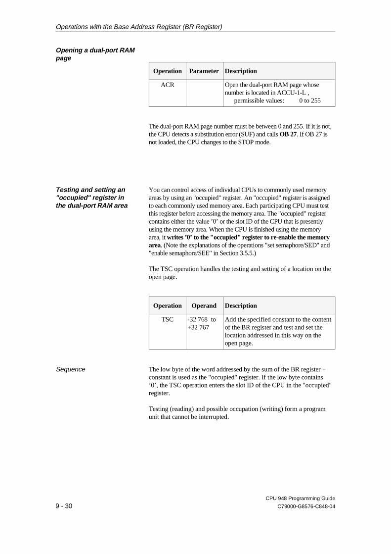
Opening a dual-port RAMpage
Operation Parameter Description
ACR Open the dual-port RAM page whosenumber is located in ACCU-1-L ,
permissible values: 0 to 255
The dual-port RAM page number must be between 0 and 255. If it is not,the CPU detects a substitution error (SUF) and calls OB 27. If OB 27 isnot loaded, the CPU changes to the STOP mode.
Testing and setting an"occupied" register inthe dual-port RAM area
You can control access of individual CPUs to commonly used memoryareas by using an "occupied" register. An "occupied" register is assignedto each commonly used memory area. Each participating CPU must testthis register before accessing the memory area. The "occupied" registercontains either the value ’0’ or the slot ID of the CPU that is presentlyusing the memory area. When the CPU is finished using the memoryarea, it writes ’0’ to the "occupied" register to re-enable the memoryarea. (Note the explanations of the operations "set semaphore/SED" and"enable semaphore/SEE" in Section 3.5.5.)
The TSC operation handles the testing and setting of a location on theopen page.
Operation Operand Description
TSC -32 768 to+32 767
Add the specified constant to the contentof the BR register and test and set thelocation addressed in this way on theopen page.
Sequence The low byte of the word addressed by the sum of the BR register +constant is used as the "occupied" register. If the low byte contains’0’, the TSC operation enters the slot ID of the CPU in the "occupied"register.
Testing (reading) and possible occupation (writing) form a programunit that cannot be interrupted.
Operations with the Base Address Register (BR Register)
CPU 948 Programming Guide
9 - 30 C79000-G8576-C848-04

Result You can evaluate the result of the TSC operation using conditioncodes CC 0 and CC 1:
CC 1 CC 0 Description
0
1
0
0
0
1
The "occupied" register contains ’0’. The CPUenters its own slot ID.
The slot ID of the CPU is already entered inthe "occupied" register.
The "occupied" register contains adifferent slot ID.
NoteAll CPUs that require synchronized access to a common globalmemory area (dual-port RAM area) must use the TSC operation.
Error reaction The location must be on the corresponding module and on thecommon page between F F400H and F FBFFH. If this is not the case,the CPU recognizes a transfer error (TRAF) and calls OB 32. IfOB 32 is not loaded, the CPU changes to the stop mode with the errorcode TRAF (ISTACK).
Load and transferoperations for the dual-port RAM memory organized in bytes
Operation Operand Description
LY CB
LY CW
LY CD
-32768 to+32767
-32768 to+32767
-32768 to+32767
add the specified constant to contentof the BR register and load the byteaddressed in this way in the open pageinto ACCU-1-LL 1) 3)
add the specified constant to contentof the BR register and load the wordaddressed in this way in the open pageinto ACCU-1-L 2) 3)
add the specified constant to contentof the BR register and load the doubleword addressed in this way in the openpage into ACCU 1 3)
Table 9-11 Operations for access to pages organized in bytes
Operations with the Base Address Register (BR Register)
CPU 948 Programming Guide
C79000-G8576-C848-04 9 - 31
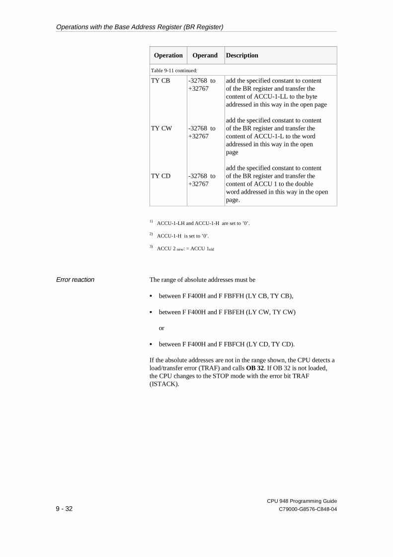
Operation Operand Description
Table 9-11 continued:
TY CB
TY CW
TY CD
-32768 to+32767
-32768 to+32767
-32768 to+32767
add the specified constant to contentof the BR register and transfer thecontent of ACCU-1-LL to the byte addressed in this way in the open page
add the specified constant to contentof the BR register and transfer thecontent of ACCU-1-L to the wordaddressed in this way in the openpage
add the specified constant to contentof the BR register and transfer thecontent of ACCU 1 to the doubleword addressed in this way in the openpage.
1) ACCU-1-LH and ACCU-1-H are set to ’0’.
2) ACCU-1-H is set to ’0’.
3) ACCU 2 new: = ACCU 1old
Error reaction The range of absolute addresses must be
•• between F F400H and F FBFFH (LY CB, TY CB),
•• between F F400H and F FBFEH (LY CW, TY CW)
or
•• between F F400H and F FBFCH (LY CD, TY CD).
If the absolute addresses are not in the range shown, the CPU detects aload/transfer error (TRAF) and calls OB 32. If OB 32 is not loaded,the CPU changes to the STOP mode with the error bit TRAF(ISTACK).
Operations with the Base Address Register (BR Register)
CPU 948 Programming Guide
9 - 32 C79000-G8576-C848-04
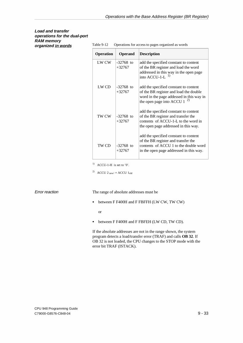
Load and transferoperations for the dual-portRAM memoryorganized in words
Operation Operand Description
LW CW
LW CD
TW CW
TW CD
-32768 to+32767
-32768 to+32767
-32768 to+32767
-32768 to+32767
add the specified constant to contentof the BR register and load the wordaddressed in this way in the open pageinto ACCU-1-L 1)
add the specified constant to contentof the BR register and load the doubleword in the page addessed in this way inthe open page into ACCU 1 2)
add the specified constant to contentof the BR register and transfer thecontents of ACCU-1-L to the word inthe open page addressed in this way.
add the specified constant to contentof the BR register and transfer thecontents of ACCU 1 to the double wordin the open page addressed in this way.
1) ACCU-1-H is set to ’0’.
2) ACCU 2 new: = ACCU 1old
Error reaction The range of absolute addresses must be
•• between F F400H and F FBFFH (LW CW, TW CW)
or
•• between F F400H and F FBFEH (LW CD, TW CD).
If the absolute addresses are not in the range shown, the systemprogram detects a load/transfer error (TRAF) and calls OB 32. IfOB 32 is not loaded, the CPU changes to the STOP mode with theerror bit TRAF (ISTACK).
Table 9-12 Operations for access to pages organized as words
Operations with the Base Address Register (BR Register)
CPU 948 Programming Guide
C79000-G8576-C848-04 9 - 33

Operations with the Base Address Register (BR Register)
CPU 948 Programming Guide
9 - 34 C79000-G8576-C848-04

Contents of Chapter 10
10.1 Multiprocessor Mode . . . . . . . . . . . . . . . . . . . . . . . . . . . . . . . . . . . . . . . . . . . . . . . . . . . . 10 - 4
10.1.1 When to use the Multiprocessor Mode . . . . . . . . . . . . . . . . . . . . . . . . . . . . . . . . . . . . . . 10 - 410.1.2 What Communications Mechanisms are Available? . . . . . . . . . . . . . . . . . . . . . . . . . . . . 10 - 410.1.3 Exchanging Data via IPC Flags . . . . . . . . . . . . . . . . . . . . . . . . . . . . . . . . . . . . . . . . . . . . 10 - 510.1.4 Exchanging Data via Handling Blocks . . . . . . . . . . . . . . . . . . . . . . . . . . . . . . . . . . . . . . 10 - 810.1.5 What needs to be Programmed for the Multiprocessor Mode? . . . . . . . . . . . . . . . . . . . 10 - 910.1.6 How to Create Data Block DB 1 . . . . . . . . . . . . . . . . . . . . . . . . . . . . . . . . . . . . . . . . . . . 10 - 910.1.7 Starting up in the Multiprocessor Mode . . . . . . . . . . . . . . . . . . . . . . . . . . . . . . . . . . . . 10 - 1310.1.8 Test Mode . . . . . . . . . . . . . . . . . . . . . . . . . . . . . . . . . . . . . . . . . . . . . . . . . . . . . . . . . . . . 10 - 14
10.2 Multiprocessor Communication . . . . . . . . . . . . . . . . . . . . . . . . . . . . . . . . . . . . . . . . . . . 10 - 15
10.2.1 Introduction. . . . . . . . . . . . . . . . . . . . . . . . . . . . . . . . . . . . . . . . . . . . . . . . . . . . . . . . . . . 10 - 1510.2.2 How the Transmitter and Receiver are Identified . . . . . . . . . . . . . . . . . . . . . . . . . . . . . 10 - 1610.2.3 Why Data is Buffered. . . . . . . . . . . . . . . . . . . . . . . . . . . . . . . . . . . . . . . . . . . . . . . . . . . 10 - 1710.2.4 How the Buffer is Processed and Managed. . . . . . . . . . . . . . . . . . . . . . . . . . . . . . . . . . 10 - 1810.2.5 System Start-Up . . . . . . . . . . . . . . . . . . . . . . . . . . . . . . . . . . . . . . . . . . . . . . . . . . . . . . . 10 - 2110.2.6 Calling Communication OBs . . . . . . . . . . . . . . . . . . . . . . . . . . . . . . . . . . . . . . . . . . . . . 10 - 2210.2.7 How to Assign Parameters to Communication OBs . . . . . . . . . . . . . . . . . . . . . . . . . . 10 - 2310.2.8 How to Evaluate the Output Parameters . . . . . . . . . . . . . . . . . . . . . . . . . . . . . . . . . . . . 10 - 24
10.3 Runtimes of the Communication OBs . . . . . . . . . . . . . . . . . . . . . . . . . . . . . . . . . . . . . . 10 - 31
10.4 INITIALIZE Function (OB 200) . . . . . . . . . . . . . . . . . . . . . . . . . . . . . . . . . . . . . . . . . . 10 - 33
10.4.1 Function. . . . . . . . . . . . . . . . . . . . . . . . . . . . . . . . . . . . . . . . . . . . . . . . . . . . . . . . . . . . . . 10 - 3310.4.2 Call Parameters . . . . . . . . . . . . . . . . . . . . . . . . . . . . . . . . . . . . . . . . . . . . . . . . . . . . . . . . 10 - 3510.4.3 Input Parameters . . . . . . . . . . . . . . . . . . . . . . . . . . . . . . . . . . . . . . . . . . . . . . . . . . . . . . . 10 - 3510.4.4 Output Parameters. . . . . . . . . . . . . . . . . . . . . . . . . . . . . . . . . . . . . . . . . . . . . . . . . . . . . . 10 - 38
10Multiprocessor Mode andCommunication in the S5-155U
CPU 948 Programming Guide
C79000-G8576-C848-04 10 - 1
10.5 SEND Function (OB 202) . . . . . . . . . . . . . . . . . . . . . . . . . . . . . . . . . . . . . . . . . . . . . . . 10 - 40
10.5.1 Function. . . . . . . . . . . . . . . . . . . . . . . . . . . . . . . . . . . . . . . . . . . . . . . . . . . . . . . . . . . . . . 10 - 4010.5.2 Call Parameters . . . . . . . . . . . . . . . . . . . . . . . . . . . . . . . . . . . . . . . . . . . . . . . . . . . . . . . . 10 - 4010.5.3 Input Parameters . . . . . . . . . . . . . . . . . . . . . . . . . . . . . . . . . . . . . . . . . . . . . . . . . . . . . . . 10 - 4010.5.4 Output Parameters. . . . . . . . . . . . . . . . . . . . . . . . . . . . . . . . . . . . . . . . . . . . . . . . . . . . . . 10 - 42
10.6 SEND TEST Function (OB 203) . . . . . . . . . . . . . . . . . . . . . . . . . . . . . . . . . . . . . . . . . 10 - 45
10.6.1 Function. . . . . . . . . . . . . . . . . . . . . . . . . . . . . . . . . . . . . . . . . . . . . . . . . . . . . . . . . . . . . . 10 - 4510.6.2 Call Parameters . . . . . . . . . . . . . . . . . . . . . . . . . . . . . . . . . . . . . . . . . . . . . . . . . . . . . . . . 10 - 4510.6.3 Input Parameters . . . . . . . . . . . . . . . . . . . . . . . . . . . . . . . . . . . . . . . . . . . . . . . . . . . . . . . 10 - 4510.6.4 Output Parameters. . . . . . . . . . . . . . . . . . . . . . . . . . . . . . . . . . . . . . . . . . . . . . . . . . . . . . 10 - 45
10.7 RECEIVE Function (OB 204) . . . . . . . . . . . . . . . . . . . . . . . . . . . . . . . . . . . . . . . . . . . . 10 - 47
10.7.1 Function. . . . . . . . . . . . . . . . . . . . . . . . . . . . . . . . . . . . . . . . . . . . . . . . . . . . . . . . . . . . . . 10 - 4710.7.2 Call Parameters . . . . . . . . . . . . . . . . . . . . . . . . . . . . . . . . . . . . . . . . . . . . . . . . . . . . . . . . 10 - 4710.7.3 Input Parameters . . . . . . . . . . . . . . . . . . . . . . . . . . . . . . . . . . . . . . . . . . . . . . . . . . . . . . . 10 - 4710.7.4 Output Parameters. . . . . . . . . . . . . . . . . . . . . . . . . . . . . . . . . . . . . . . . . . . . . . . . . . . . . . 10 - 48
10.8 RECEIVE TEST Function (OB 205). . . . . . . . . . . . . . . . . . . . . . . . . . . . . . . . . . . . . . . 10 - 51
10.8.1 Function. . . . . . . . . . . . . . . . . . . . . . . . . . . . . . . . . . . . . . . . . . . . . . . . . . . . . . . . . . . . . . 10 - 5110.8.2 Call Parameters . . . . . . . . . . . . . . . . . . . . . . . . . . . . . . . . . . . . . . . . . . . . . . . . . . . . . . . . 10 - 5110.8.3 Input Parameters . . . . . . . . . . . . . . . . . . . . . . . . . . . . . . . . . . . . . . . . . . . . . . . . . . . . . . . 10 - 5110.8.4 Output Parameters. . . . . . . . . . . . . . . . . . . . . . . . . . . . . . . . . . . . . . . . . . . . . . . . . . . . . . 10 - 51
10.9 Applications . . . . . . . . . . . . . . . . . . . . . . . . . . . . . . . . . . . . . . . . . . . . . . . . . . . . . . . . . . 10 - 53
10.9.1 Calling the Special Function OB using Function Blocks . . . . . . . . . . . . . . . . . . . . . . . 10 - 5310.9.2 Transferring Data Blocks . . . . . . . . . . . . . . . . . . . . . . . . . . . . . . . . . . . . . . . . . . . . . . . . 10 - 6010.9.3 Extending the IPC Flag Area . . . . . . . . . . . . . . . . . . . . . . . . . . . . . . . . . . . . . . . . . . . . . 10 - 66
Contents
CPU 948 Programming Guide
10 - 2 C79000-G8576-C848-04
10Multiprocessor Mode and Communication in the S5-155U
At the beginning of this chapter, you will see when you can use themultiprocessor mode and which data exchange is possible in thismode. The chapter provides you with information about programmingfor multiprocessor operation (Section 10.1).The second part of the chapter provides you with detailed instructionsand examples of exchanging larger amounts of data in themultiprocessor mode (multiprocessor communication Sections 10.2 to10.9).
CPU 948 Programming Guide
C79000-G8576-C848-04 10 - 3
10.1 Multiprocessor Mode
Definitions of terms The S5-155U is set up for multiprocessor operation as soon as youplug in a coordinator module, regardless of how many CPUs orCP/IPs are plugged in. The CPUs must be plugged in without anygaps between them.
10.1.1When to use theMultiprocessor Mode
•• If your user program is too large for one CPU and there is notenough memory, distribute your program on several CPUs.
•• When a particular part of your system has to be processedespecially fast, separate the appropriate program part from the totalprogram and run it on its own fast CPU.
•• When your system consists of several parts that you can separateeasily and control independently, let CPU 1 process system part 1,CPU 2 process system part 2, etc.
For more information on multiprocessing, read the information in yoursystem manual. This will help you to decide which CPUs are best suitedfor your problem.
10.1.2What CommunicationsMechanisms are Available?
•• "Interprocessor communication flags" are available for cyclicexchange of binary data between CPUs (CPU 948, CPU 946/947,CPU 928B, CPU 928 and CPU 922) or between CPUs andcommunications processors (CPs).
•• For the exchange of large amounts of data (e.g., entire data blocks)between the CPU 948, CPU 946/947, CPU 928B, CPU 928 andCPU 922 you are supported by the "special functions formultiprocessing" OB 200 to OB 205 (for more information refer toSection 10.2).
•• "Handling blocks" are available for communication withintelligent input/output modules (IPs) and with CPs (Thesehandling blocks must be ordered separately).
Multiprocessor Mode
CPU 948 Programming Guide
10 - 4 C79000-G8576-C848-04
10.1.3Exchanging Data via IPCFlags
Interprocessor communication (IPC) flags are available for cyclicexchange of binary data. They are used mainly for transmittinginformation byte by byte.
Data is transferred as follows:
CPU(s) ↔ CPU(s)
CPU(s) ↔ Communications processor(s)
The system program transfers IPC flags once per cycle. For datatransfer between CPUs, the IPC flags are buffered physically on thecoordinator.
IPC flags are bytes that are transferred. You define them in DB 1 foreach CPU as IPC input or output flags. If, for example, you havedefined flag byte 50 on the CPU 1 as an IPC output flag byte, itssignal state is transferred cyclically via the coordinator to the CPU onwhich the flag byte F 50 is defined as an IPC input flag byte.
NoteThere is no error message when the IPC flag byte existsphysically but is only written by one CPU and never read out andvice-versa.
Memory area With the CPU 948 the memory area for the IPC flags in thecoordinator and the CPs covers the addresses F F200H to F F2FFH.On a CPU/communications processor there are 256 available IPC flagbytes.
Jumper settings To avoid double assignments you must group the 256 available IPCflag bytes on the COR or CP modules. Fields of 32 bytes can beenabled or disabled (your system manual contains information aboutsetting the jumpers).
Multiprocessor Mode
CPU 948 Programming Guide
C79000-G8576-C848-04 10 - 5
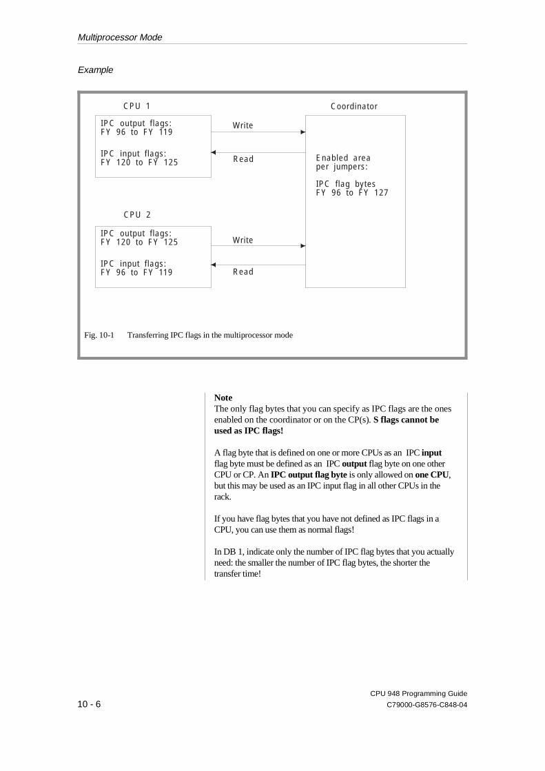
Example
NoteThe only flag bytes that you can specify as IPC flags are the onesenabled on the coordinator or on the CP(s). S flags cannot beused as IPC flags!
A flag byte that is defined on one or more CPUs as an IPC inputflag byte must be defined as an IPC output flag byte on one otherCPU or CP. An IPC output flag byte is only allowed on one CPU,but this may be used as an IPC input flag in all other CPUs in therack.
If you have flag bytes that you have not defined as IPC flags in aCPU, you can use them as normal flags!
In DB 1, indicate only the number of IPC flag bytes that you actuallyneed: the smaller the number of IPC flag bytes, the shorter thetransfer time!
CPU 1
IPC output f lags:FY 96 to FY 119
IPC input f lags:FY 120 to FY 125
CPU 2
Coordinator
IPC output f lags:FY 120 to FY 125
IPC input f lags:FY 96 to FY 119
Wri te
Read
Wri te
Read
Enabled areaper jumpers:
IPC flag bytesFY 96 to FY 127
Fig. 10-1 Transferring IPC flags in the multiprocessor mode
Multiprocessor Mode
CPU 948 Programming Guide
10 - 6 C79000-G8576-C848-04
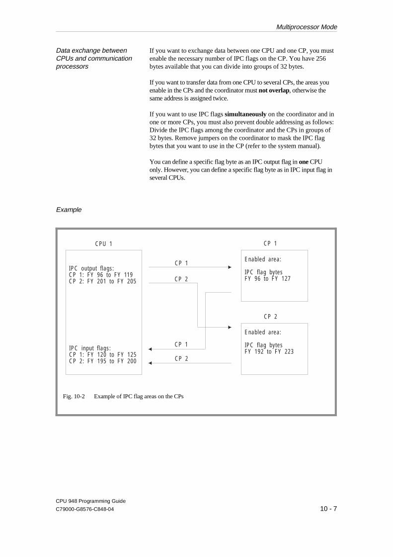
Data exchange betweenCPUs and communicationprocessors
If you want to exchange data between one CPU and one CP, you mustenable the necessary number of IPC flags on the CP. You have 256bytes available that you can divide into groups of 32 bytes.
If you want to transfer data from one CPU to several CPs, the areas youenable in the CPs and the coordinator must not overlap, otherwise thesame address is assigned twice.
If you want to use IPC flags simultaneously on the coordinator and inone or more CPs, you must also prevent double addressing as follows: Divide the IPC flags among the coordinator and the CPs in groups of32 bytes. Remove jumpers on the coordinator to mask the IPC flagbytes that you want to use in the CP (refer to the system manual).
You can define a specific flag byte as an IPC output flag in one CPUonly. However, you can define a specific flag byte as in IPC input flag inseveral CPUs.
Example
CPU 1
Enabled area:
IPC flag bytesFY 96 to FY 127
Enabled area:
IPC flag bytesFY 192 to FY 223
CP 1
CP 2
CP 1
CP 2
CP 1
CP 2
IPC output f lags:CP 1: FY 96 to FY 119CP 2: FY 201 to FY 205
IPC input f lags:CP 1: FY 120 to FY 125CP 2: FY 195 to FY 200
Fig. 10-2 Example of IPC flag areas on the CPs
Multiprocessor Mode
CPU 948 Programming Guide
C79000-G8576-C848-04 10 - 7

Transmitting IPC flags inmultiprocessor operation
At the end of each program cycle, along with the updating of theprocess image, the CPU transmits the IPC flags specified in DB 1when the coordinator signals the CPU that it can access the S5 bus.
The coordinator allocates the bus enable signal to each CPU insequence. When a CPU has access to the S5 bus, it can transmit onlyone byte. Because of this interleaved transmission, related (bytegroups) IPC flag information can be separated and subsequentlyprocessed with old or incorrect values.
If you want to transfer information that takes up more than one byte,you can prevent corruption of data by setting a parameter in extendeddata block DX 0. This parameter uses semaphores to ensure that allIPC flags specified in DB 1 are transferred in groups (see Chapter 7).While one CPU is transmitting IPC flags, another CPU cannotinterrupt it. Because the next CPU has to wait to transmit its data,cyclic program processing of this CPU is delayed accordingly.Under certain circumstances, the setting you make in DX 0 canincrease the cycle time considerably.
Multiprocessorcommunication
For transferring data blocks or more exactly fields of data with a sizeof max. 64 byte (= 32 data words), the following special functions areintegrated in the CPU:
•• OB 200: INITIALIZE: preassign
•• OB 202: SEND: send a data field
•• OB 203: SEND TEST: test sending capacity
•• OB 204: RECEIVE: receive a data field
•• OB 205: RECEIVE TEST: test receiving capacity
10.1.4Exchanging Data viaHandling Blocks
Handling blocks are capable of multiprocessing. A special parameterassignment for the multiprocessor mode is not necessary. For moreinformation on handling blocks refer to the appropriate manual.
Multiprocessor Mode
CPU 948 Programming Guide
10 - 8 C79000-G8576-C848-04

10.1.5What needs to beProgrammed for theMultiprocessor Mode?
•• To allow the coordinator to coordinate access by the individualCPUs to the I/O area, you must program data block DB 1. Evenif the CPU does not use I/Os or the IPC flags, a (empty) DB 1must exist (for more information refer to Section 10.1.6)
•• Data block DX 0 must also exist. Program this so that processinterrupts via input byte IB 0 are disabled and the system interruptsare activated.
10.1.6How to Create Data BlockDB 1
For multiprocessing, you must program DB 1 for each CPU. Thisestablishes the inputs, outputs (byte addresses 0 to 127) and IPCinput and output flags with which each CPU works.
NoteThe system program recognizes only the inputs and outputsdefined in DB 1 when it updates the process image!
Inputting or changing DB 1 •• Create/modify DB 1 on the PG using the DB 1 screen form
or
•• by editing DB 1 as a data block on the PG and then transferring itto the CPU.
NoteThe CPU accepts the entered or changed DB 1 only after a coldrestart!
Using the DB 1 screen form 1. Select the editor for the DB 1 screen form on your PG(refer to Fig. 10-3).
2. Enter the required values for "digital inputs" etc. as decimal numbers.
Multiprocessor Mode
CPU 948 Programming Guide
C79000-G8576-C848-04 10 - 9
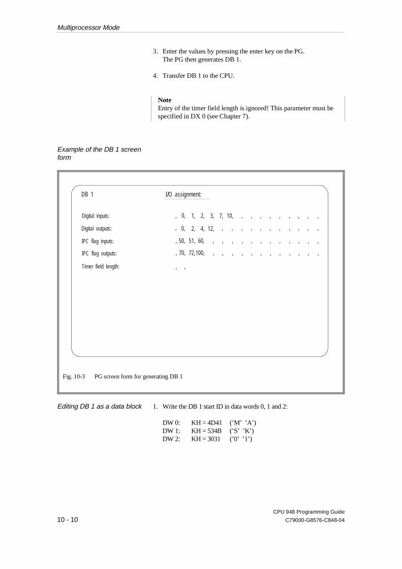
3. Enter the values by pressing the enter key on the PG.The PG then generates DB 1.
4. Transfer DB 1 to the CPU.
NoteEntry of the timer field length is ignored! This parameter must bespecified in DX 0 (see Chapter 7).
Example of the DB 1 screenform
Editing DB 1 as a data block 1. Write the DB 1 start ID in data words 0, 1 and 2:
DW 0: KH = 4D41 (’M’ ’A’)DW 1: KH = 534B (’S’ ’K’)DW 2: KH = 3031 (’0’ ’1’)
DB 1
0, 1, 2, 3, 7, 10,
2, 4, 12,0,
50, 51, 60,
70, 72,100,
,
,
,
,
,
,
,
,
,
,
,
,
,
,
,
,
,
,
,
,
,
,
,
,
,
,
,
,
,
,
,
,
,
,
,
,
,
,
,
,
,
,
,
,
,
,
,
,
,
,
I/O assignment:
Digital inputs:
Digital outputs:
IPC flag inputs:
IPC flag outputs:
Timer field length:
Fig. 10-3 PG screen form for generating DB 1
Multiprocessor Mode
CPU 948 Programming Guide
10 - 10 C79000-G8576-C848-04

2. Type in the individual operand areas (from data word 3 onwards).Before each operand area, you must specify an ID. The possible ID words are as follows:
ID word for digital inputs KH = DE00ID word for digital outputs KH = DA00ID word for IPC input flags KH = CE00ID word for IPC output flags KH = CA00
After each ID word, use fixed-point format to list the numbers of theinputs and outputs used.
3. Complete the entries with the DB 1 end ID "KH = EEEE" andtransfer DB 1 to the CPU.
NoteYou can make the DB 1 entries in any order. Remember that theprocess image of the inputs and outputs is updated in the reverseorder to which you store the addresses in DB 1 (i.e. the last entryis updated first).Multiple entries of the same bytes (e.g., for test purposes) arepossible. The system program makes multiple updates of the processimages of bytes that are entered more than once.
Example of editing DB 1
DB1 FD: CPU948ST.S5D
0: KH = 4D41; DW 0-2: 1: KH = 534B; Start ID 2: KH = 3031; for DB 1 3: KH = DE00; ID word for digital inputs 4: KF = +00000; Input byte 0 5: KF = +00001; Input byte 1 6: KF = +00002; Input byte 2 7: KF = +00003; Input byte 3 8: KF = +00007; . 9: KF = +00010; Input byte 1010: KH = DA00; ID word for digital outputs11: KF = +00000; Output byte 012: KF = +00002; Output byte 213: KF = +00004; .14: KF = +00012; Output byte 1215: KH = CE00; ID word for IPC flag inputs16: KF = +00050; Flag byte 5017: KF = +00051; .18: KF = +00060; Flag byte 6019: KH = CA00; ID word for IPC flag outputs20: KF = +00070; Flag byte 7021: KF = +00072; .22: KF = +00100; Flag byte 10023: KH = EEEE; End ID24:
Multiprocessor Mode
CPU 948 Programming Guide
C79000-G8576-C848-04 10 - 11

Entering DB 1 The system program adopts DB 1 during a cold restart. The systemprogram checks to see if the inputs and outputs or IPC flags indicatedin DB 1 exist in their corresponding modules. If they are not presentthere, a DB 1 error causes the CPU to go into the STOP mode and theSTOP LED flashes slowly. The CPU no longer processes yourprogram.
After you program DB 1 and the CPU accepts it during a cold restart,the following rules apply:
•• Only the inputs and outputs indicated in DB 1 can access peripheralmodules via the process images (L.../T... ...IB, ...IW, ...ID, ...QB,...QW, ...QD operations and logic operations with inputs and outputs).Access to process image addresses not entered in DB 1 causeaddressing errors.
•• You can load peripheral bytes directly by bypassing the processimage using the L PB/L PY, L PW, L OY, L OW operations for allacknowledging inputs, regardless of entries in DB 1.
•• You can transfer directly (T PB/T PY, T PW) to bytes 0 to 127 onlyfor the outputs indicated in DB 1. This is because the process image isalso written to during direct transfer. Writing to I/O addresses notentered in DB 1 causes an addressing error.
•• Transfer without a process image :Direct transfer to byte addresses >127 is possible regardless of theentries in DB 1.Direct transfer of byte addresses of the extended I/Os (T OY,T OW) is also possible regardless of the entries in DB 1.
Multiprocessor Mode
CPU 948 Programming Guide
10 - 12 C79000-G8576-C848-04
10.1.7Starting up in theMultiprocessor Mode
You can start the coordinator for multiprocessing in one of thefollowing ways:
Initial status: The RUN/STOP switch of each CPU is in the RUN position. The RUN/STOP switch
on the coordinator is in the STOP position.
Handling: Move the RUN/STOP switch on the coordinatorfrom STOP to RUN. (Starting the S5-155U in multiprocessor operation simply by starting the coordinator is possible only if the coordinator itself caused the controller to change to the STOP mode).
or:
Initial status: The RUN/STOP switch of each CPU is inthe RUN position as well as that of thecoordinator.
Handling: Use the PG START function to start the CPU that caused the STOP in the requiredrestart type.
Starting up individual CPUs The restart type that each CPU now uses depends on what took placewhile the CPU was in the STOP mode. Some CPUs need MANUALWARM RESTART, others, a COLD RESTART.
If the CPU settings were not changed in that time, execute a manualwarm restart.
NoteDue to the various restart types, incorrect signal statuses can betransferred from one CPU to another via the IPC flags. This couldhappen if the controller was in cycle prior to entering the STOPmode. Prevent this by programming the start-up organizationblocks OB 20, OB 21 and OB 22 appropriately.
You can call special function block OB 223 to check whether thestart-up types of all the CPUs are the same (refer to Chapter 6).
Multiprocessor Mode
CPU 948 Programming Guide
C79000-G8576-C848-04 10 - 13

Power failure/return of power When power is shut off and then restored, the coordinator startsautomatically. In this case, all CPUs execute an AUTOMATICWARM RESTART or an AUTOMATIC COLD RESTART ,depending on the setting in DX 0 (see Chapter 7).
The start-up of the individual CPUs in multiprocessor operation issynchronized. Each CPU waits until all others have ended theirinitialization phase. Then they begin their cycle simultaneously.However, you can use a setting in DX 0 to cancel start-upsynchronization.
10.1.8Test Mode Proceed as follows:
1. Make sure that the "test mode" function is enabled on the coordinator.
2. Switch the mode selector on the COR from STOP to TEST.The BASP LED goes off.
3. Go through a COLD RESTART or WARM RESTART on theCPUs you want to change to the RUN mode.
Special features of testoperation
In test operation, you can run CPUs individually or in any combination.CPUs in the STOP mode cannot disable the entire PLC.
Start-up of individual CPUs is not synchronized in test operation. TheCPUs begin their cyclic operation at different times according to thelength of the start-up organization blocks OB 20, OB 21 or OB 22.
If an error occurs in one CPU during test operation, only that CPU goesinto the STOP mode. The error does not affect the other CPUs.
WarningSince no CPU can output the BASP signal in case of an errorin the test mode, the test mode must be switched inactive aftersuccessful installation to avoid a critical or even dangeroussituation arising in the system.
Multiprocessor Mode
CPU 948 Programming Guide
10 - 14 C79000-G8576-C848-04

10.2 Multiprocessor Communication
Definition Multiprocessor communication means the exchange of largeramounts of data (data blocks) between CPUs operating in themultiprocessor mode. The COR C is necessary for multiprocessorcommunication.
10.2.1Introduction To transfer data blocks, or to be more precise, blocks of data with a
maximum length of 64 bytes (= 32 data words), you can use thefollowing special functions that are integrated in the CPU:
•• OB 200: INITIALIZE: preassign
•• OB 202: SEND: send a field of data
•• OB 203: SEND TEST: test sending capacity
•• OB 204: RECEIVE: receive a data field
•• OB 205: RECEIVE TEST: test receiving capacity
The special function OBs, OB 200 and OB 202 to OB 205 are simplycalled "communication OBs" in the following sections.
Required knowledge To use these functions, you only require basic knowledge of the STEP 5 programming language and the way in which SIMATIC S5programmable controllers operate. You can obtain this basicinformation from the publications listed in the Further Reading.
Basic sequence To transfer data, you must activate the SEND function on thetransmitting CPU and the RECEIVE function on the receiving CPU.The data words of a DB or DX data block located in the transmittingCPU are transported via the coordinator 923C to the receiving CPUone after the other and written to the DB or DX data block with thesame number and under the same data word address; i.e. thisrepresents a "1:1" copy operation.
Data fields The amount of data that can be transferred with the SEND and RECEIVE functions is normally 32 words. If the block length (without header) is not a multiple of 32 words, thelast field of data to be transferred is an exception and is less than 32words long.
Multiprocessor Communication
CPU 948 Programming Guide
C79000-G8576-C848-04 10 - 15
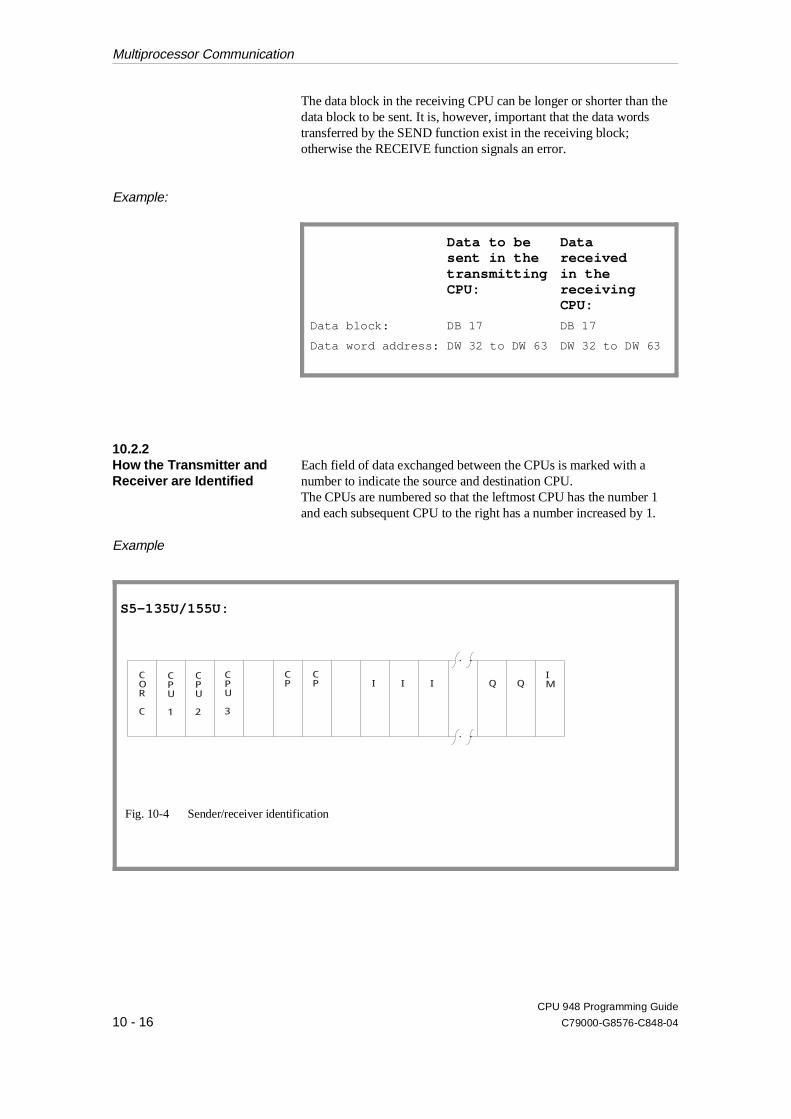
The data block in the receiving CPU can be longer or shorter than thedata block to be sent. It is, however, important that the data wordstransferred by the SEND function exist in the receiving block;otherwise the RECEIVE function signals an error.
Example:
10.2.2How the Transmitter andReceiver are Identified
Each field of data exchanged between the CPUs is marked with anumber to indicate the source and destination CPU.The CPUs are numbered so that the leftmost CPU has the number 1and each subsequent CPU to the right has a number increased by 1.
Example
S5-135U/155U:
Data to besent in the transmitting CPU:
Datareceivedin thereceivingCPU:
Data block: DB 17 DB 17
Data word address: DW 32 to DW 63 DW 32 to DW 63
COR
C
CPU
1
CPU
2
CPU
3
CP
CP
IM
. .
. .
I QI I Q
Fig. 10-4 Sender/receiver identification
Multiprocessor Communication
CPU 948 Programming Guide
10 - 16 C79000-G8576-C848-04
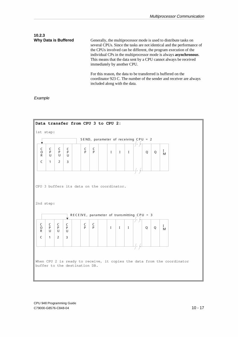
10.2.3Why Data is Buffered Generally, the multiprocessor mode is used to distribute tasks on
several CPUs. Since the tasks are not identical and the performance ofthe CPUs involved can be different, the program execution of theindividual CPs in the multiprocessor mode is always asynchronous.This means that the data sent by a CPU cannot always be receivedimmediately by another CPU.
For this reason, the data to be transferred is buffered on thecoordinator 923 C. The number of the sender and receiver are alwaysincluded along with the data.
Example
Data transfer from CPU 3 to CPU 2:
1st step:
CPU 3 buffers its data on the coordinator.
2nd step:
When CPU 2 is ready to receive, it copies the data from the coordinatorbuffer to the destination DB.
COR
C
CPU
1
CPU
2
CPU
3
CP
CP I
M
. .
. .
I
SEND, parameter of receiv ing CPU = 2
QI I Q
COR
C
CPU
1
CPU
2
CPU
3
CP
CP I
M
. .
. .
I
RECEIVE, parameter of t ransmit t ing CPU = 3
QI I Q
Multiprocessor Communication
CPU 948 Programming Guide
C79000-G8576-C848-04 10 - 17
10.2.4How the Buffer isProcessed and Managed
Principle The buffer is based on the FIFO principle (first in - first out, queueprinciple). The data is received in the order in which it is sent. Thisapplies to each individual link (identified by the transmitting andreceiving CPU) and is independent of other links.
Data protection The buffer is battery-backed; this means that the "automatic warmrestart following a power down" is possible without any restrictions. Aloss of power during a data transfer does not cause any loss of data inthe programmable controller.
Management The coordinator 923 C has a memory capacity of 48 data fields eachwith a fixed length of 32 words. The INITIALIZE function assignsthese fields to individual CPU links.Each memory field can receive exactly one field of data. The lengthof the data can be from 1 data word to 32 data words. A data field isentered in a memory field by a SEND function and read out again by aRECEIVE function.The number of memory fields assigned to a link is directly related to theparameters for the transmitting capacity (SEND, SEND TEST function)and receiving capacity (RECEIVE, RECEIVE TEST function).
The transmitting capacity indicates how many of the memory fieldsreserved for a link are free at any particular time.
The receiving capacity indicates how many of the memory fieldsreserved for a link are occupied at any particular time.
The sum of the transmitting and receiving capacity is always equal tothe number of memory fields reserved for a link.
Multiprocessor Communication
CPU 948 Programming Guide
10 - 18 C79000-G8576-C848-04
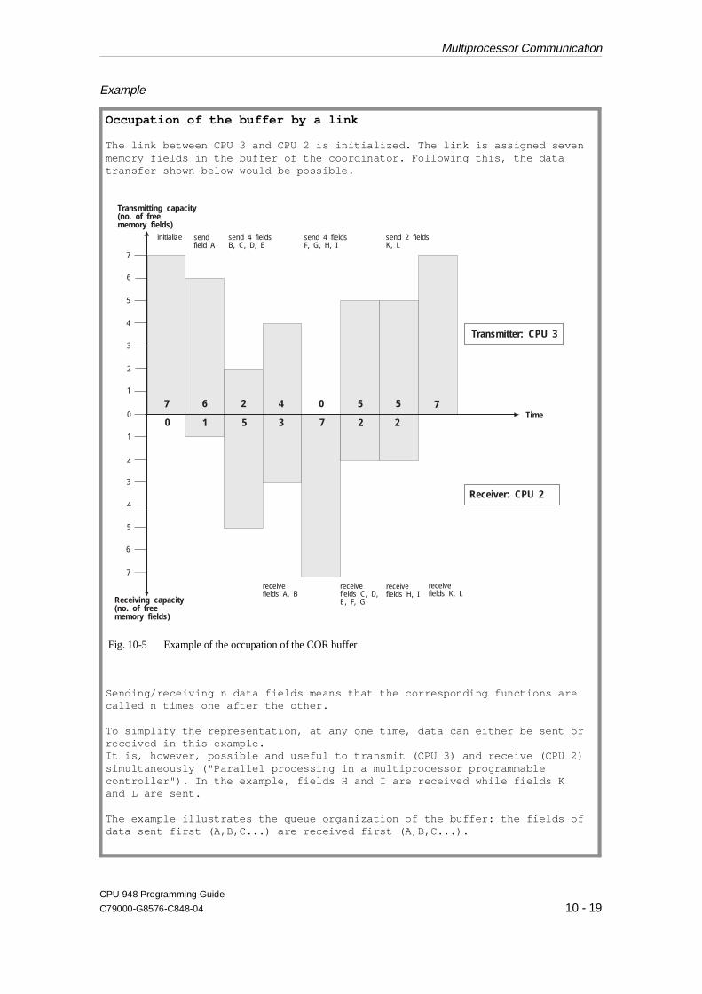
Example
Occupation of the buffer by a link
The link between CPU 3 and CPU 2 is initialized. The link is assigned sevenmemory fields in the buffer of the coordinator. Following this, the datatransfer shown below would be possible.
Sending/receiving n data fields means that the corresponding functions arecalled n times one after the other.
To simplify the representation, at any one time, data can either be sent orreceived in this example. It is, however, possible and useful to transmit (CPU 3) and receive (CPU 2)simultaneously ("Parallel processing in a multiprocessor programmablecontroller"). In the example, fields H and I are received while fields Kand L are sent.
The example illustrates the queue organization of the buffer: the fields ofdata sent first (A,B,C...) are received first (A,B,C...).
7
7
6
6
5
5
4
4
3
3
2
2
1
1
0
Transmitter: CPU 3
initialize
0
0
sendfield A
send 4 fieldsB, C, D, E
send 4 fieldsF, G, H, I
send 2 fieldsK, L
Time
receivefields A, B
receivefields C, D,E, F, G
receivefields H, I
receivefields K, L
Transmitting capacity(no. of freememory fields)
Receiving capacity(no. of freememory fields)
6 2
5
7 7
1
4
3 7 2 2
5 5
Receiver: CPU 2
Fig. 10-5 Example of the occupation of the COR buffer
Multiprocessor Communication
CPU 948 Programming Guide
C79000-G8576-C848-04 10 - 19
Summary Buffering data on the coordinator COR 923C allows the asynchronousoperation of transmitting and receiving CPUs and compensates fortheir different processing speeds.
Since the capacity of the buffer is limited, the receiver should check"often" and "regularly" whether there are data in the buffer (RECEIVETEST function, receiving capacity > 0) and should attempt to fetchstored data (RECEIVE function). Ideally, the RECEIVE functionshould be repeated until the receiving capacity is zero. This means thatthe transmitted data are not buffered for a longer period of time andthat the receiver always has the current data. This also means thatmemory fields remain free (the transmitting capacity is increased) andprevents the sender from being blocked (i.e. when the transmittingcapacity is zero).
NoteA receiving capacity of zero represents the ideal state (i.e. alltransmitted data have been fetched by the receiver), on the otherhand a transmitting capacity of zero indicates incorrect planning,as follows:
- the SEND function is called too often,
- the RECEIVE function is not called often enough
or
- there are not enough memory fields assigned to the link.The capacity of the buffer is insufficient to compensate tempo-rary imbalances in the frequency with which the CPUs trans- mit and receive data.
Multiprocessor Communication
CPU 948 Programming Guide
10 - 20 C79000-G8576-C848-04

10.2.5System Start-Up If you require multiprocessor communication, then all CPUs involved
must go through the same STOP-RUN transition (= RESTART), i.e.all the CPUs go through a COLD RESTART or all CPUs go through aWARM RESTART.
You must make sure that the restart of at least all the CPUs involvedin the communication is uniform (see Section 10.1.7), in thefollowing ways:
•• direct operation (front switch, programmer),
•• parameter assignment (DX 0)
and/or
•• programming (using the special function organization block OB 223"stop if non-uniform restarts occur in the multiprocessor mode")
COLD RESTART In organization block OB 20 (COLD RESTART) only one CPU mustset up the buffer (in the COR 923C) using the INITIALIZE function.Any existing data is lost.Following this, i.e. during the RESTART, you can call the SEND,SEND TEST, RECEIVE, RECEIVE TEST functions in the individualCPUs. With appropriate programming, you must make sure that thisonly occurs after the buffer in the coordinator has been correctlyinitialized.On completion of the RESTART, i.e. in the RUN mode, the userprogram is processed from the beginning, i.e. from the first operationin OB 1.
WARM RESTART You must not use the INITIALIZE function in the organization blocksOB 21 (MANUAL WARM RESTART) and OB 22 (AUTOMATICWARM RESTART). Calling the SEND, SEND TEST, RECEIVE,RECEIVE TEST functions can cause problems (refer to the followingsections).
On completion of the WARM RESTART, i.e. in the RUN mode, theuser program is not processed from the start, but from the point atwhich it was interrupted. The point of interruption can, for example,be within the SEND function.
Multiprocessor Communication
CPU 948 Programming Guide
C79000-G8576-C848-04 10 - 21
10.2.6Calling Communication OBs
Proceed as follows:
1. Call the INITIALIZE function only in the cold restartorganization block OB 20 on one CPU.
2. Call the SEND, SEND TEST, RECEIVE, RECEIVE TEST functions either only within the cyclic program or only within thetime-driven program.
Double call Depending on the assignment of parameters in DX 0 ("interrupts atoperation boundaries"), and the type of program execution (WARMRESTART, interrupt handling, e.g. OB 26 for cycle time error) it ispossible that one of the functions INITIALIZE, SEND, SEND TEST,RECEIVE and RECEIVE TEST can be interrupted. If a user interface inserted at the point of interruption also contains oneof the functions SEND, SEND TEST, RECEIVE and RECEIVETEST an illegal call (double call) is recognized and an error issignalled (error number 67, Section 10.2.8).
Parallel processing Once you have completed the assignment of the buffer (INITIALIZEfunction), you can execute the functions SEND, SEND TEST, RECEIVE and RECEIVE TEST in any combination and with anyparameter assignment in all the CPUs simultaneously and parallel toeach other.
Taking a single link (e.g. from CPU 2 to CPU 3) it is possible toexecute the SEND function (CPU 2) and the RECEIVE function(CPU 3) simultaneously. While CPU 2 is sending data fields to thecoordinator, CPU 3 can already receive (fetch) buffered data filedsfrom the coordinator.
Areas occupied The communication OBs do not require a working area (for bufferingvariables) and do not call data blocks. They do, of course, access areascontaining parameters, although only the parameters marked as outputparameters are modified.
Multiprocessor Communication
CPU 948 Programming Guide
10 - 22 C79000-G8576-C848-04

Results bits The results bits (CC 1/CC 0, RLO etc.) are influenced by thecommunication OBs. For more detailed information refer to Section10.2.8.
Changes in the ACCUs •• CPU 922, CPU 928, CPU 928B: The contents of ACCU 1 to ACCU 4 and the
contents of the registers are not affected by the communication OBs.
•• CPU 946/947,CPU 948: The contents of all registers and ACCU 1, 2
and 3 remain the same, only the contents ofACCU 4 are affected.
10.2.7How to Assign Parametersto Communication OBs The communication OBs have the following types of parameter:
•• input parameters,
•• output parameters
and
•• call parameters.
Input and output parameters are located in a maximum 10 byte longdata field in the F flag area. The data field is divided into an area forinput parameters and an area for output parameters.
Input parameters The input parameters specify how a function is handled. All or part ofthe parameters are read out by communication OBs and evaluated, nowrite access takes place.
Output parameters The output parameters contain all the information that the callingprogram needs about the result of a job, e.g. error bits.Some or all of the output parameters are written to by thecommunication OBs, this area is not read.
NoteYou can assign a flag area with 10 flag bytes for allcommunications functions. The functions themselves requiredifferent numbers of bytes. Refer to the description of the singlefunctions (Section 10.4ff).
Multiprocessor Communication
CPU 948 Programming Guide
C79000-G8576-C848-04 10 - 23
Call parameters For all communication OBs the number of the first flag byte in thedata field (= pointer to data field) in ACCU-1-L is transferred as thecall parameter. Permitted values are 0 to 246.
Example
10.2.8How to Evaluate the Output Parameters
Among other things, the output parameters indicate whether or not afunction could be executed and if not they indicate the reason for thetermination of the function.
Condition codes The INITIALIZE, SEND, SEND TEST, RECEIVE and RECEIVETEST functions affect the condition codes (see programminginstructions for your CPUs, general notes on the STEP 5 operations):
•• the OV and OS bits (word condition codes) are always cleared,
•• the OR, STA, ERAB bits (bit condition codes) are always cleared,
•• RLO, CC 1 and CC 0 indicate whether a function has been executedcorrectly and completely.
Data field with parameters for the RECEIVE function (OB 204)
FY x + 0: transmitting CPU input parameterFY x + 1: — not used
FY x + 2: condition code byte output parameterFY x + 3: receiving capacity output parameter
FY x + 4: block ID output parameterFY x + 5: block number output parameter
FY x + 6: address of the first output parameterFY x + 7: received data word output parameter
FY x + 8: address of the last output parameterFY x + 9: received data word output parameter
This example illustrates that the number of the first F flag byte in thedata field must not be higher than FY 246, since otherwise the parameterfield of up to 10 bytes would exceed the limits of the flag area (FY 255).
Multiprocessor Communication
CPU 948 Programming Guide
10 - 24 C79000-G8576-C848-04
Condition codesEvaluation Meaning
RLO CC 1 CC 0
0 0 0 JC= Function executedcompletely and correctly
1 0 0 JC= Function aborted,pointer to data fieldillegal (>246)
Function abortedowing to an initializationconflict
1 0 1 JC= andJM=
Function abortedowing to an error(error number 1 to 9)
1 1 0 JC= andJP=
Function abortedowing to a warning(warning number 1 or 2)
In the following sections, it is assumed that the pointer to the datafield contains a correct value. The first byte of the output parameterprovides detailed information about the cause of termination.
Condition code byte Bit no. 7 6 5 4 3 2 1 0
W E I 0 Number
W = 1: Warning
E = 1: Error
I = 1: Initialization conflict
Number: - of a warning- of an error- of an initialization conflict
Table 10-1 Condition codes of the communication OBs
Multiprocessor Communication
CPU 948 Programming Guide
C79000-G8576-C848-04 10 - 25

The first byte in the field of the output parameters (condition codebyte) also indicates whether or not a function has been correctly andcompletely executed. This byte contains detailed information aboutthe cause of termination of a function.Assuming that at least the pointer to the data field contains a correctvalue, this byte is always relevant.
If the function has been executed correctly and completely, all the bitsare cleared (= 0), and all other output parameters are relevant.
If the function is aborted with a warning (bit number 7 = 1), only thecondition code for the transmitting/receiving capacity is relevant,other output parameters (if they exist) are unchanged.
If the function is aborted owing to an error (bit number 6 = 1) or aninitialization conflict (bit number 5 = 1), all other output parametersremain unchanged.
Evaluation of the code byte The identifiers ’W’, ’E’ and ’I’ indicate the significance of thenumbers.Apart from this bit-by-bit evaluation, it is also possible to interpret thewhole condition code byte as a fixed point number without sign. Ifyou interpret the condition code byte as a byte, the groups of numbershave the following significance:
Number group Significance
0
33 to 42
65 to 73
129 to 130
Function executed correctly and completely
Function aborted owing to an initializationconflict
Function aborted owing to an error
Function aborted owing to a warning
Errors are detected and indicated in the ascending order of the errornumbers. This means that several errors may have occurred although(currently) only one is indicated. The other errors are then indicated byfurther calls.
Table 10-2 Code byte for the communication OBs/number groups
Multiprocessor Communication
CPU 948 Programming Guide
10 - 26 C79000-G8576-C848-04

Example
Initialization conflict An initialization conflict can only occur with the INITIALIZATIONfunction. If a conflict occurs, you must modify the program or theparameters.
Initialization conflict numbers (evaluation of the condition code byteas a byte):
Cond.codebyte
Significance
33 The pages required for multiprocessor communication(numbers 252 to 255) are not or not all available.
34 The pages required for multiprocessor communication(numbers 252 to 255) are defective.
35 The parameter "automatic/manual" is illegal.The following errors are possible:
- the "automatic/manual" ID is less than 1,- the "automatic/manual" ID is greater than 2.
36 The parameter "number of CPUs" is illegal.The following errors are possible:
- the number of CPUs is less than 2,- the number of CPUs is greater than 4.
37 The parameter "block ID" is illegal.The following errors are possible:
- the block ID is less than 1,- the block ID is greater than 2.
38 The parameter "block number" is incorrect, since it is a datablock with a special significance.The following errors are possible:
- if block ID = 1 DB 0, DB 1- if block ID = 2 : DX 0
39 The parameter "block number " is incorrect, since the datablock does not exist.
40 The parameter "start address of the assignment list" is toohigh or the data block is too short.
The SEND function indicates an error and is notexecuted. If you then make program and/orparameter modifications and the SEND functionagain indicates an error with a higher numberthan previously, you can assume that you havecorrected one of several errors.
Table 10-3 Condition code byte: Initialization conflict numbers
Multiprocessor Communication
CPU 948 Programming Guide
C79000-G8576-C848-04 10 - 27
Cond.codebyte
Significance
Table 10-3 continued:
41 The assignment list in the data block is not correctlystructured.
42 The sum of the assigned memory fields is greater than 48.
Errors If an error occurs, you must change the program/parameters.
Error numbers (evaluation of the condition code byte as a byte):
Cond.codebyte
Significance
65 The parameter "receiving CPU" (SEND, SEND TEST)is illegal. The following errors are possible:
- The number of the receiving CPU is greater than 4,- the number of the receiving CPU is less than 1,- the number of the receiving CPU is the same as the
CPU’s own number.
66 The parameter "transmitting CPU" (RECEIVE, RECEIVETEST) is illegal. The following errors are possible:
- The number of the transmitting CPU is greater than 4,- the number of the transmitting CPU is less than 1,- the number of the transmitting CPU is the same as the
CPU’s own number.
67 The special function organization block call is wrong(SEND, RECEIVE, SEND TEST, RECEIVE TEST). Thefollowing errors are possible:
- Secondary error, since the INITIALIZE function couldnot be called or was terminated by an initializationconflict.
- Double call: the call for this function (SEND, SEND TEST, RECEIVE or RECEIVE TEST) is illegal, since one of these functions INITIALIZE, SEND, SEND TEST, RECEIVE or RECEIVE TEST has already been called in this CPU in a lower processing level (i.e. cyclic program execution).
- The CPU’s own number is incorrect (system datacorrupted); following power down/power up the CPUnumber is generated again by the system program.
Table 10-4 Condition code byte: Error numbers
Multiprocessor Communication
CPU 948 Programming Guide
10 - 28 C79000-G8576-C848-04
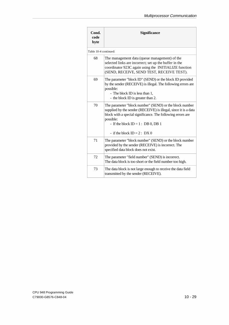
Cond.codebyte
Significance
Table 10-4 continued:
68 The management data (queue management) of theselected links are incorrect; set up the buffer in thecoordinator 923C again using the INITIALIZE function(SEND, RECEIVE, SEND TEST, RECEIVE TEST).
69 The parameter "block ID" (SEND) or the block ID providedby the sender (RECEIVE) is illegal. The following errors arepossible:
- The block ID is less than 1,- the block ID is greater than 2.
70 The parameter "block number" (SEND) or the block numbersupplied by the sender (RECEIVE) is illegal, since it is a datablock with a special significance. The following errors arepossible:
- If the block ID = 1 : DB 0, DB 1
- if the block ID = 2 : DX 0
71 The parameter "block number" (SEND) or the block numberprovided by the sender (RECEIVE) is incorrect. Thespecified data block does not exist.
72 The parameter "field number" (SEND) is incorrect.The data block is too short or the field number too high.
73 The data block is not large enough to receive the data fieldtransmitted by the sender (RECEIVE).
Multiprocessor Communication
CPU 948 Programming Guide
C79000-G8576-C848-04 10 - 29
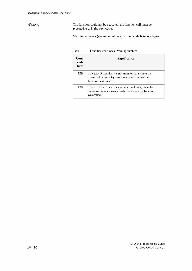
Warning The function could not be executed; the function call must berepeated, e.g. in the next cycle.
Warning numbers (evaluation of the condition code byte as a byte):
Cond.codebyte
Significance
129 The SEND function cannot transfer data, since the transmitting capacity was already zero when the function was called.
130 The RECEIVE function cannot accept data, since thereceiving capacity was already zero when the function was called.
Table 10-5 Condition code bytes: Warning numbers
Multiprocessor Communication
CPU 948 Programming Guide
10 - 30 C79000-G8576-C848-04
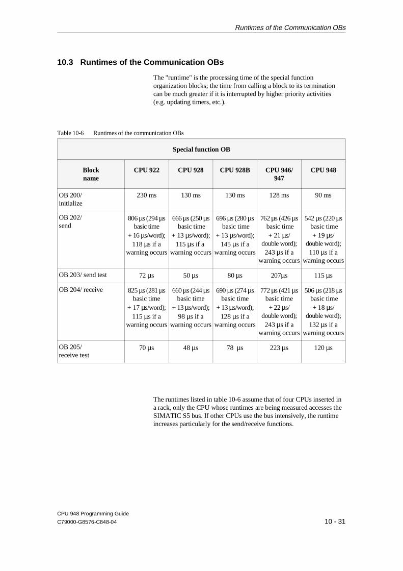
10.3 Runtimes of the Communication OBs
The "runtime" is the processing time of the special functionorganization blocks; the time from calling a block to its terminationcan be much greater if it is interrupted by higher priority activities(e.g. updating timers, etc.).
Special function OB
Blockname
CPU 922 CPU 928 CPU 928B CPU 946/947
CPU 948
OB 200/initialize
230 ms 130 ms 130 ms 128 ms 90 ms
OB 202/send
806 µs (294 µsbasic time
+ 16 µs/word);118 µs if a
warning occurs
666 µs (250 µs basic time
+ 13 µs/word);115 µs if a
warning occurs
696 µs (280 µs basic time
+ 13 µs/word);145 µs if a
warning occurs
762 µs (426 µs basic time+ 21 µs/
double word);243 µs if a
warning occurs
542 µs (220 µs basic time+ 19 µs/
double word);110 µs if a
warning occurs
OB 203/ send test 72 µs 50 µs 80 µs 207µs 115 µs
OB 204/ receive 825 µs (281 µsbasic time
+ 17 µs/word);115 µs if a
warning occurs
660 µs (244 µsbasic time
+ 13 µs/word);98 µs if a
warning occurs
690 µs (274 µsbasic time
+ 13 µs/word);128 µs if a
warning occurs
772 µs (421 µsbasic time+ 22 µs/
double word);243 µs if a
warning occurs
506 µs (218 µs basic time+ 18 µs/
double word);132 µs if a
warning occurs
OB 205/receive test
70 µs 48 µs 78 µs 223 µs 120 µs
The runtimes listed in table 10-6 assume that of four CPUs inserted ina rack, only the CPU whose runtimes are being measured accesses theSIMATIC S5 bus. If other CPUs use the bus intensively, the runtimeincreases particularly for the send/receive functions.
Table 10-6 Runtimes of the communication OBs
Runtimes of the Communication OBs
CPU 948 Programming Guide
C79000-G8576-C848-04 10 - 31

Transfer time An important factor of a link (e.g. from CPU 1 to CPU 2) is the totaldata transfer time. This is made up of the following components:
•• time required to send (see runtime),
•• length of time the data are buffered (on the COR 923C coordinator)
and
•• the time required to receive data (see runtime)
The length of time that the data are "in transit" is largelydependent on the length of time that the data is buffered andtherefore on the structure of the user program (see "BufferingData").
Runtimes of the Communication OBs
CPU 948 Programming Guide
10 - 32 C79000-G8576-C848-04
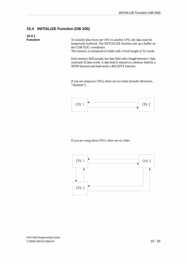
10.4 INITIALIZE Function (OB 200)
10.4.1Function To transfer data from one CPU to another CPU, the data must be
temporarily buffered. The INITIALIZE function sets up a buffer onthe COR 923C coordinator.The memory is initialized in fields with a fixed length of 32 words.
Each memory field accepts one data field with a length between 1 dataword and 32 data words. A data field is entered in a memory field by aSEND function and read out by a RECEIVE function.
If you are using two CPUs, there are two links (transfer directions,"channels"):
If you are using three CPUs, there are six links:
CPU 1 CPU 2
CPU 2
CPU 3
CPU 1
INITIALIZE Function (OB 200)
CPU 948 Programming Guide
C79000-G8576-C848-04 10 - 33
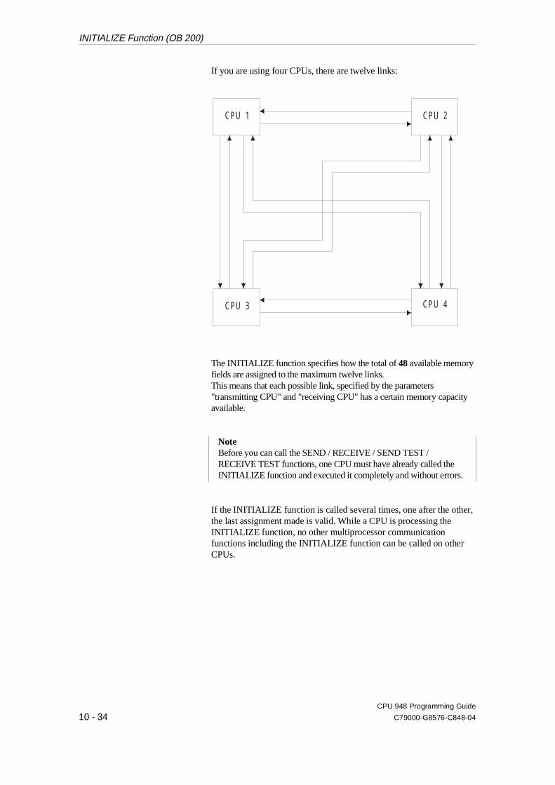
If you are using four CPUs, there are twelve links:
The INITIALIZE function specifies how the total of 48 available memoryfields are assigned to the maximum twelve links.This means that each possible link, specified by the parameters"transmitting CPU" and "receiving CPU" has a certain memory capacityavailable.
NoteBefore you can call the SEND / RECEIVE / SEND TEST /RECEIVE TEST functions, one CPU must have already called theINITIALIZE function and executed it completely and without errors.
If the INITIALIZE function is called several times, one after the other,the last assignment made is valid. While a CPU is processing theINITIALIZE function, no other multiprocessor communicationfunctions including the INITIALIZE function can be called on otherCPUs.
CPU 3 CPU 4
CPU 1 CPU 2
INITIALIZE Function (OB 200)
CPU 948 Programming Guide
10 - 34 C79000-G8576-C848-04
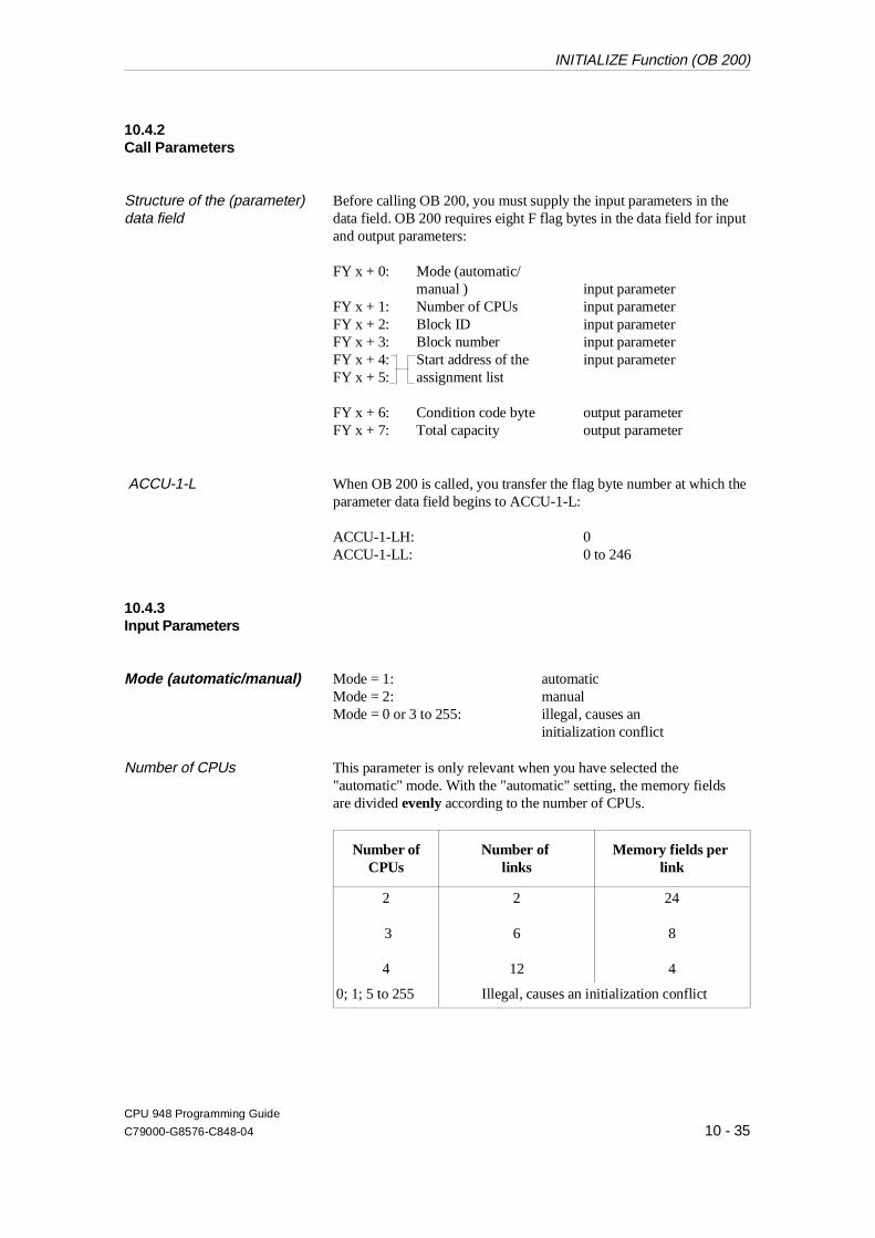
10.4.2Call Parameters
Structure of the (parameter)data field
Before calling OB 200, you must supply the input parameters in thedata field. OB 200 requires eight F flag bytes in the data field for inputand output parameters:
FY x + 0: Mode (automatic/manual ) input parameter
FY x + 1: Number of CPUs input parameterFY x + 2: Block ID input parameterFY x + 3: Block number input parameterFY x + 4: Start address of the input parameterFY x + 5: assignment list
FY x + 6: Condition code byte output parameterFY x + 7: Total capacity output parameter
ACCU-1-L When OB 200 is called, you transfer the flag byte number at which theparameter data field begins to ACCU-1-L: ACCU-1-LH: 0ACCU-1-LL: 0 to 246
10.4.3Input Parameters
Mode (automatic/manual) Mode = 1: automatic Mode = 2: manualMode = 0 or 3 to 255: illegal, causes an
initialization conflict
Number of CPUs This parameter is only relevant when you have selected the"automatic" mode. With the "automatic" setting, the memory fieldsare divided evenly according to the number of CPUs.
Number ofCPUs
Number of links
Memory fields per link
2
3
4
2
6
12
24
8
4
0; 1; 5 to 255 Illegal, causes an initialization conflict
INITIALIZE Function (OB 200)
CPU 948 Programming Guide
C79000-G8576-C848-04 10 - 35
Block ID, block number,address assignment list
The parameters are only relevant if you select the "manual" mode.You must then create an assignment list in a data block in which the48 available memory fields (or less) are assigned to the maximum 12links. This function is particularly useful when some CPUs transfermore data than others. The CPUs not involved in the multiprocessor communication do notneed and should not have memory fields assigned to them.The parameters
•• block ID,
•• block number
and
•• start address of the assignment list
specify where the assignment list is stored.
Block ID ID = 1: DB data blockID = 2: DX data blockID = 0 or 3 to 255 : illegal, causes an
initialization conflict
Block number For the block number, you specify the number of the DB or DX datablock in which the assignment list is stored.
Start address of theassignment list:
Along with the block ID and number, this specifies the area (or moreprecisely, the start address of the area) in the data block in which theassignment list is stored.As the address of the assignment list, specify the data word number atwhich the assignment list begins in flag bytes FY x+4 (high byte) andFY x+5 (low byte).
INITIALIZE Function (OB 200)
CPU 948 Programming Guide
10 - 36 C79000-G8576-C848-04

Assignment list With the assignment list, you specify how many of the existing 48memory fields are to be assigned to the links.
The list is not changed by the system program. It has the followingstructure.
Data word Format Value Significance
DW n + 0DW n + 1DW n + 2DW n + 3
KSKYKYKY
S12 , a3 , b4 , c
Transmitter = CPU 1Receiver = CPU 2Receiver = CPU 3Receiver = CPU 4
DW n + 4DW n + 5DW n + 6DW n + 7
KSKYKYKY
S21 , d3 , e4 , f
Transmitter = CPU 2Receiver = CPU 1Receiver = CPU 3Receiver = CPU 4
DW n + 8DW n + 9DW n + 10DW n + 11
KSKYKYKY
S31 , g2 , h4 , i
Transmitter = CPU 3Receiver = CPU 1Receiver = CPU 2Receiver = CPU 4
DW n + 12DW n + 13DW n + 14DW n + 15
KSKYKYKY
S41 , k2 , l3 , m
Transmitter = CPU 4Receiver = CPU 1Receiver = CPU 2Receiver = CPU 3
Instead of the lower case letters a to m (in bold face) numbers between 0and 48 must be inserted depending on the number of assigned memoryfields. The sum of these numbers must not exceed 48.
NoteYou must keep to the structure shown in table 10-7 even if you haveless than four CPUs.
Table 10-7 Assignment list for OB 200 (initialize)
INITIALIZE Function (OB 200)
CPU 948 Programming Guide
C79000-G8576-C848-04 10 - 37
Example
10.4.4Output Parameters
Condition code byte This byte informs you whether the INITIALIZE function wasexecuted correctly and completely.
Initialization conflict The initialization conflicts listed are recognized and indicated by thefunction in the ascending order of their numbers.
If an initialization conflict occurs, you must change theprogram/parameters.
All the numbers listed in Table 10-3 can occur in the condition codebyte.
You have three CPUs in your rack, CPU 2 sends a lot of data to the othertwo CPUs. The other two CPUs, however, only send a small amount of databack to CPU 2 as acknowledgements in a logical handshake. There is no dataexchange between CPU 1 and CPU 3 .
The assignment list is stored in data block DB 40 from DW 0 onwards and hasthe following parameters:
DB40 FD: CPU948ST.S5D
0: KS = S1; Transmitter: CPU 1 1: KY = 2, 2; Receiver: CPU 2/2 fields 2: KY = 3, 0; Receiver: CPU 3/no field 3: KY = 4, 0; Receiver: CPU 4 (does not exist)/no field 4: KS = S2; Transmitter: CPU 2 5: KY = 1, 22 ; Receiver: CPU 1/22 fields 6: KY = 3, 22; Receiver: CPU 3/22 fields 7: KY = 4, 0; Receiver: CPU 4 (does not exist)/no field 8: KS = S3; Transmitter: CPU 3 9: KY = 1, 0; Receiver: CPU 1/no field10: KY = 2, 2; Receiver: CPU 2/2 fields11: KY = 4, 0; Receiver: CPU 4 (does not exist)/no field12: KS = S4; Transmitter: CPU 4 (does not exist)13: KY = 1, 0; Receiver: CPU 1/no field14: KY = 2, 0; Receiver: CPU 2/no field15: KY = 3,0; Receiver: CPU 3/no field16:
INITIALIZE Function (OB 200)
CPU 948 Programming Guide
10 - 38 C79000-G8576-C848-04
Errors The "error" number group cannot occur with the INITIALIZEfunction.
Warning The "warning" number group cannot occur with the INITIALIZEfunction.
Total capacity This parameter specifies how many of the 48 available memory fieldsare assigned to links.In the "automatic" mode, this parameter always has the value 48. In the"manual" mode, it can have a value less than 48. This means that existingmemory capacity is not used.
INITIALIZE Function (OB 200)
CPU 948 Programming Guide
C79000-G8576-C848-04 10 - 39
10.5 SEND Function (OB 202)
10.5.1Function The SEND function transfers a data field to the buffer of the
COR 923C coordinator. It also indicates how many data fields can stillbe sent or buffered.
10.5.2Call Parameters
Structure of the (parameter)data field
Before calling OB 202 you must specify the input parameters in the datafield. OB 202 requires six F flag bytes in the data field for input andoutput parameters:
FY x + 0: receiving CPU input parameterFY x + 1: block ID input parameterFY x + 2: block number input parameterFY x + 3: field number input parameter
FY x + 4: condition code byte output parameterFY x + 5: transmitting capacity output parameter
ACCU-1-L When OB 202 is called, transfer the flag byte at which the parameterdata field begins to ACCU-1-L:
ACCU-1-LH: 0ACCU-1-LL: 0 to 246
10.5.3Input Parameters
Receiving CPU CPU number of the receiver (destination); the permitted value is between1 and 4 but must be different from the CPU’s own number.
SEND Function (OB 202)
CPU 948 Programming Guide
10 - 40 C79000-G8576-C848-04

Block ID ID = 1: DB data blockID = 2: DX data blockID = 0 or 3 to 255: illegal, causes an
error message
Block number The block number, along with the block ID and the field numberspecifies the area from which the data to be sent is taken (and where itis to be stored in the receiving CPU).
Remember that certain data blocks have a special significance, forexample, DB 0, DB 1 or DX 0 (see programming instructions for yourCPUs). These data blocks must therefore not be used for the datatransfer described here!If you attempt to use these block numbers, the function is aborted withan error message.
Field number The field number indicates the area in which the data to be sent islocated.
Field number
Data area
First data word Last data word
01
23
45
67
89::
DW 0DW 32
DW 64DW 96
DW 128DW 160
DW 192DW 224
DW 256DW 288
::
DW 31DW 63
DW 95DW 127
DW 159DW 191
DW 223DW 255
DW 287DW 319
::
SEND Function (OB 202)
CPU 948 Programming Guide
C79000-G8576-C848-04 10 - 41

The following situations are possible:
•• DB is longer than source area:If the data block is sufficiently long, you obtain a 32-word longarea per field as shown in the table above.
•• DB is too short:If the end of the data block is within the selected field, in the lastfield an area with a length between 1 and 32 words will betransferred.
•• Field is outside the DB:If the first data word address of a field is not within the length ofthe data block, the SEND function detects and indicates an error.
Example
10.5.4Output Parameters
Condition code byte This byte informs you whether the SEND function was executedcorrectly and completely.
Initialization conflict Has no significance with the SEND function.
Data block with a length of 80 words: DW 0 to DW 74, 5 words are required for the block header.
Field no.: First data word: Last data word: Length:
0 DW 0 DW 31 32 words1 DW 32 DW 63 32 words
2 DW 64 DW 74 11 words
3 andhigher Incorrect parameter assignment
SEND Function (OB 202)
CPU 948 Programming Guide
10 - 42 C79000-G8576-C848-04
Errors When the SEND function is called, the following error numbers(evaluation of the condition code byte) can occur:
Conditioncode byte
Significance
65 The parameter "receiving CPU" is illegal.The following errors are possible:
- The number of the receiving CPU is greater than 4,- The number of the receiving CPU is less than 1,- The number of the receiving CPU is the same as
the CPU’s own number.
67 The special function organization block call is wrong.The following errors are possible:
- Secondary error, since the INITIALIZE functioncould not be called or was terminated by aninitialization conflict.
- Double call: the call for this function, SEND, SENDTEST, RECEIVE or RECEIVE TEST is illegal,since one of the functions INITIALIZE, SEND, SEND TEST, RECEIVE or RECEIVE TEST hasalready been called in this CPU in a lower processinglevel (e.g. cyclic program processing).
- The CPU’s own number is incorrect (system datacorrupted)following power down/power up the CPU numberis generated again by the system program.
68 The management data (queue management) of the selected links are incorrect; set up the buffer inthe coordinator 923C again using the INITIALIZEfunction.
69 The parameter "block ID" is illegal.The following errors are possible:
- The block ID is less than 1,- the block ID is greater than 2.
70 The parameter "block number" is illegal, since it is a datablock with a special significance.The following errors are possible:
- If the block ID = 1 : DB 0, DB 1- If the block ID = 2 : DX 0
71 The parameter "block number" is incorrect.The specified data block does not exist.
72 The parameter "field number" is incorrect. The datablock is too short or the field number too high.
SEND Function (OB 202)
CPU 948 Programming Guide
C79000-G8576-C848-04 10 - 43
Warning The function could be executed; the function call must be repeated,e.g. in the next cycle.
The following warning numbers (evaluation of the condition codebyte) can occur:
Conditioncode byte
Significance
129 The SEND function cannot transfer data, since thetransmitting capacity was already zero when thefunction was called.
Transmitting capacity The "transmitting capacity" indicates how many data fileds can still besent and buffered.
SEND Function (OB 202)
CPU 948 Programming Guide
10 - 44 C79000-G8576-C848-04

10.6 SEND TEST Function (OB 203)
10.6.1Function The SEND TEST function determines the number of free memory
fields in the buffer of the COR 923C coordinator.Depending on this number m, the SEND function can be called mtimes to transfer m data fields.
10.6.2Call Parameters
Structure of the (parameter)data field
Before calling OB 203, you must specify the input parameters in thedata field. OB 203 requires 4 F flag bytes in the data field for inputand output parameters:
FY x + 0: receiving CPU input parameterFY x + 1: — not used
FY x + 2: condition code byte output parameterFY x + 3: transmitting capacity output parameter
ACCU-1-L When OB 203 is called, transfer the flag byte number at which theparameter data field begins to ACCU-1-L:
ACCU-1-LH: 0ACCU-1-LL: 0 to 246
10.6.3Input Parameters
Receiving CPU The CPU’s own number and the number of the receiving CPU identifythe link for which the transmitting capacity is determined.
10.6.4Output Parameters
Condition code byte This byte indicates whether the SEND TEST function was executedcorrectly and completely.
SEND TEST Function (OB 203)
CPU 948 Programming Guide
C79000-G8576-C848-04 10 - 45
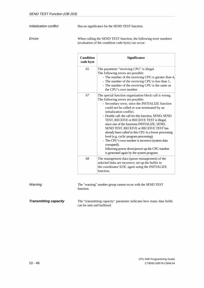
Initialization conflict Has no significance for the SEND TEST function.
Errors When calling the SEND TEST function, the following error numbers(evaluation of the condition code byte) can occur:
Conditioncode byte
Significance
65 The parameter "receiving CPU" is illegal.The following errors are possible:
- The number of the receiving CPU is greater than 4,- The number of the receiving CPU is less than 1,- The number of the receiving CPU is the same as
the CPU’s own number.
67 The special function organization block call is wrong.The following errors are possible:
- Secondary error, since the INITIALIZE functioncould not be called or was terminated by aninitialization conflict.
- Double call: the call for this function, SEND, SENDTEST, RECEIVE or RECEIVE TEST is illegal,since one of the functions INITIALIZE, SEND, SEND TEST, RECEIVE or RECEIVE TEST hasalready been called in this CPU in a lower processinglevel (e.g. cyclic program processing).
- The CPU’s own number is incorrect (system datacorrupted);following power down/power up the CPU numberis generated again by the system program.
68 The management data (queue management) of the selected links are incorrect; set up the buffer inthe coordinator 923C again using the INITIALIZEfunction.
Warning The "warning" number group cannot occur with the SEND TESTfunction.
Transmitting capacity The "transmitting capacity" parameter indicates how many data fieldscan be sent and buffered.
SEND TEST Function (OB 203)
CPU 948 Programming Guide
10 - 46 C79000-G8576-C848-04
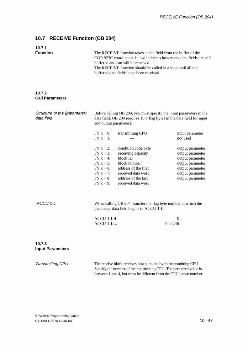
10.7 RECEIVE Function (OB 204)
10.7.1Function The RECEIVE function takes a data field from the buffer of the
COR 923C coordinator. It also indicates how many data fields are stillbuffered and can still be received.The RECEIVE function should be called in a loop until all thebuffered data fields have been received.
10.7.2Call Parameters
Structure of the (parameter)data field
Before calling OB 204, you must specify the input parameters in thedata field. OB 204 requires 10 F flag bytes in the data field for inputand output parameters:
FY x + 0: transmitting CPU input parameterFY x + 1: — not used
FY x + 2: condition code byte output parameterFY x + 3: receiving capacity output parameterFY x + 4: block ID output parameterFY x + 5: block number output parameterFY x + 6: address of the first output parameterFY x + 7: received data word output parameterFY x + 8: address of the last output parameterFY x + 9: received data word
ACCU-1-L When calling OB 204, transfer the flag byte number at which theparameter data field begins to ACCU-1-L:
ACCU-1-LH: 0ACCU-1-LL: 0 to 246
10.7.3Input Parameters
Transmitting CPU The receive block receives data supplied by the transmitting CPU.Specify the number of the transmitting CPU. The permitted value isbetween 1 and 4, but must be different from the CPU’s own number.
RECEIVE Function (OB 204)
CPU 948 Programming Guide
C79000-G8576-C848-04 10 - 47
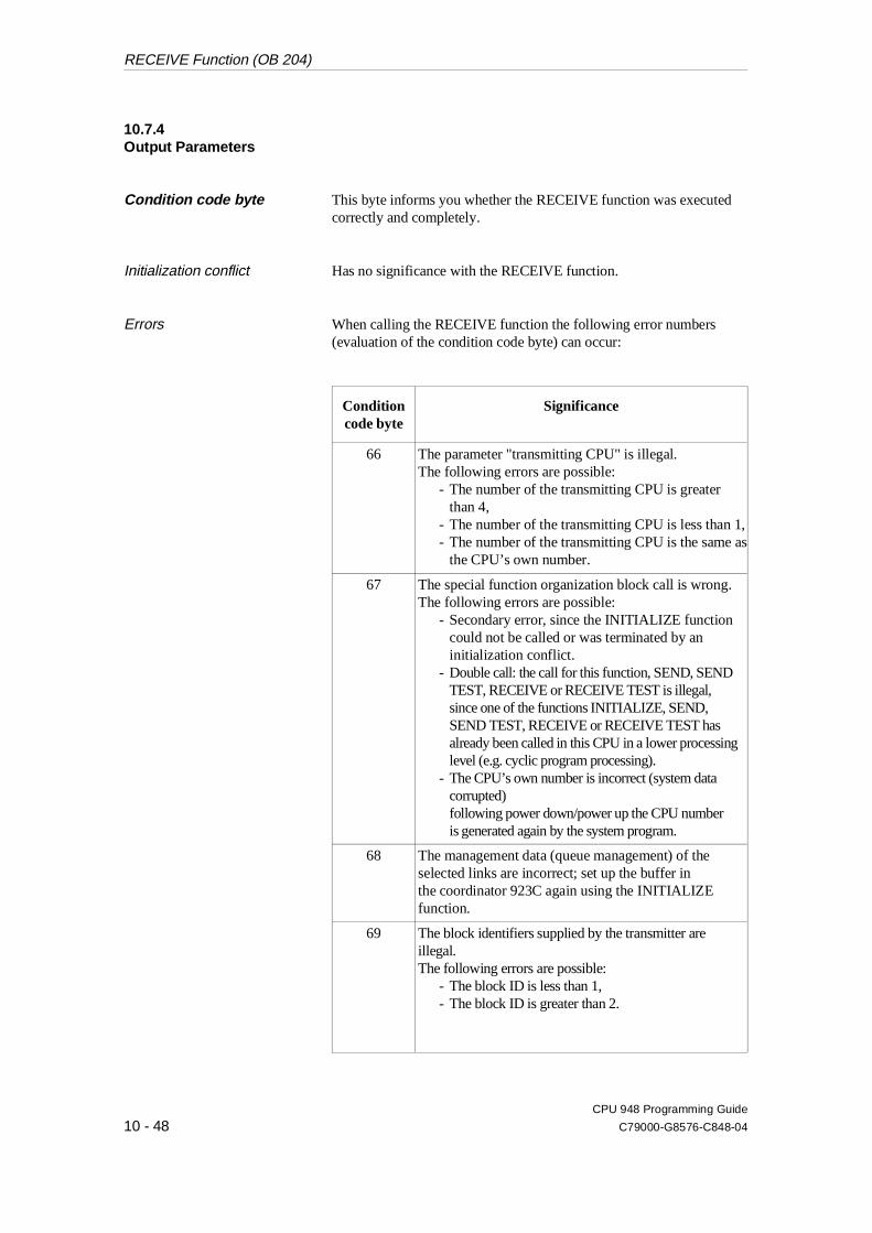
10.7.4Output Parameters
Condition code byte This byte informs you whether the RECEIVE function was executedcorrectly and completely.
Initialization conflict Has no significance with the RECEIVE function.
Errors When calling the RECEIVE function the following error numbers(evaluation of the condition code byte) can occur:
Conditioncode byte
Significance
66 The parameter "transmitting CPU" is illegal.The following errors are possible:
- The number of the transmitting CPU is greater than 4,
- The number of the transmitting CPU is less than 1,- The number of the transmitting CPU is the same as
the CPU’s own number.
67 The special function organization block call is wrong.The following errors are possible:
- Secondary error, since the INITIALIZE functioncould not be called or was terminated by aninitialization conflict.
- Double call: the call for this function, SEND, SENDTEST, RECEIVE or RECEIVE TEST is illegal,since one of the functions INITIALIZE, SEND, SEND TEST, RECEIVE or RECEIVE TEST hasalready been called in this CPU in a lower processinglevel (e.g. cyclic program processing).
- The CPU’s own number is incorrect (system datacorrupted)following power down/power up the CPU numberis generated again by the system program.
68 The management data (queue management) of the selected links are incorrect; set up the buffer inthe coordinator 923C again using the INITIALIZEfunction.
69 The block identifiers supplied by the transmitter areillegal.The following errors are possible:
- The block ID is less than 1,- The block ID is greater than 2.
RECEIVE Function (OB 204)
CPU 948 Programming Guide
10 - 48 C79000-G8576-C848-04
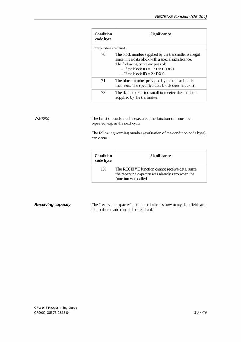
Conditioncode byte
Significance
Error numbers continued:
70 The block number supplied by the transmitter is illegal,since it is a data block with a special significance.The following errors are possible:
- If the block ID = 1 : DB 0, DB 1- If the block ID = 2 : DX 0
71 The block number provided by the transmitter isincorrect. The specified data block does not exist.
73 The data block is too small to receive the data fieldsupplied by the transmitter.
Warning The function could not be executed; the function call must berepeated, e.g. in the next cycle.
The following warning number (evaluation of the condition code byte)can occur:
Conditioncode byte
Significance
130 The RECEIVE function cannot receive data, since the receiving capacity was already zero when the function was called.
Receiving capacity The "receiving capacity" parameter indicates how many data fields arestill buffered and can still be received.
RECEIVE Function (OB 204)
CPU 948 Programming Guide
C79000-G8576-C848-04 10 - 49
Block ID: ID = 1: DB data blockID = 2: DX data blockID = 0 or 3 to 255: illegal, causes an
error message
Block number Block number of the DB/DX in which the received data are stored(and from which they are taken by the SEND function in thetransmitting CPU).
Remember that the receive data blocks must be in a random accessmemory, using read-only memories (EPROM) might possibly serve apractical purpose for transmit data blocks only.
Address of the first received data word
Data word number within the DB/DX in which the firsttransferred/received data word was stored.
Address of the last received data word
Data word number within the DB/DX in which the lasttransferred/received data word was stored.
NoteThe difference between the addresses of the first and last dataword transferred is a maximum of 31, since a maximum of 32data words can be transferred per function call.
RECEIVE Function (OB 204)
CPU 948 Programming Guide
10 - 50 C79000-G8576-C848-04

10.8 RECEIVE TEST Function (OB 205)
10.8.1Function The RECEIVE TEST function determines the number of occupied
memory fields in the buffer of the COR 923C coordinator. Dependingon this number m, the RECEIVE function can be called m times toreceive m data fields.
10.8.2Call Parameters
Structure of the (parameter)data field
Before calling OB 205, you must specify the input parameters in thedata field. OB 205 requires 4 F flag bytes in the data field for inputand output parameters:
FY x + 0: transmitting CPU input parameterFY x + 1: — not used
FY x + 2: condition code byte output parameterFY x + 3: receiving capacity output parameter
ACCU-1-L When calling OB 204, transfer the flag byte number at which theparameter data field begins to ACCU-1-L:
ACCU-1-LH: 0ACCU-1-LL: 0 to 246
10.8.3Input Parameters
Transmitting CPU The CPU’s own number and the number of the transmitting CPU identifythe link for which the receiving capacity is determined.
10.8.4Output Parameters
Condition code byte This byte indicates whether the RECEIVE TEST function was executedcorrectly and completely.
Initialization conflict Has no significance with the RECEIVE TEST function.
RECEIVE TEST Function (OB 205)
CPU 948 Programming Guide
C79000-G8576-C848-04 10 - 51
Errors When calling the RECEIVE TEST function, the following errornumbers (evaluation of the condition code byte) can occur:
Conditioncode byte
Significance
66 The parameter "transmitting CPU" is illegal.The following errors are possible:
- The number of the transmitting CPU is greater than 4,
- The number of the transmitting CPU is less than 1,- The number of the transmitting CPU is the same as
the CPU’s own number.
67 The special function organization block call is wrong.The following errors are possible:
- Secondary error, since the INITIALIZE functioncould not be called or was terminated by aninitialization conflict.
- Double call: the call for this function, SEND, SENDTEST, RECEIVE or RECEIVE TEST is illegal,since one of the functions INITIALIZE, SEND, SEND TEST, RECEIVE or RECEIVE TEST hasalready been called in this CPU in a lower processinglevel (e.g. cyclic program processing).
- The CPU’s own number is incorrect (system datacorrupted);following power down/power up the CPU numberis generated again by the system program.
68 The management data (queue management) of the selected links are incorrect; set up the buffer inthe coordinator 923C again using the INITIALIZEfunction.
Warning The "warning" number group cannot occur with the RECEIVE TESTfunction.
Receiving capacity The "receiving capacity" parameter indicates how many data fields can bereceived and buffered.
RECEIVE TEST Function (OB 205)
CPU 948 Programming Guide
10 - 52 C79000-G8576-C848-04
10.9 Applications
Based on examples, this section explains how to programmultiprocessor communication.
NoteIf you use the function blocks listed below and service interruptson your CPU (e.g. with OB 2) remember to save the "scratchpadflags" at the start of interrupt servicing and to write them backwhen the interrupt is completed.This also applies to the setting "interrupts at block boundaries",since the call of the special function organization blocksrepresents a block boundary.
10.9.1Calling the Special Function OB using Function Blocks
The following five function blocks (FB 200 and FB 202 to FB 205)contain the call for the corresponding special function organization blockfor multiprocessor communication (OB 200 and OB 202 to OB 205). The numbers of the function blocks are not fixed and can be changed.The parameters of the special function OBs are transferred as actualparameters when the function blocks are called. The direct call of thespecial function organization blocks is faster, however, is more difficultto read owing to the absence of formal parameters
FB no. FB name Function
FB 200
FB 202
FB 203
FB 204
FB 205
INITIAL
SEND
SEND-TST
RECEIVE
RECV-TST
Set up buffer
Send a data field
Test sending capacity
Receive a data field
Test receiving capacity
The flag area from FY 246 to maximum FY 255 is used by the functionblocks as a parameter field for the special function organization blocks.
The exact significance of the input and output parameters is explainedin the description of the special function organization blocks.
Applications
CPU 948 Programming Guide
C79000-G8576-C848-04 10 - 53
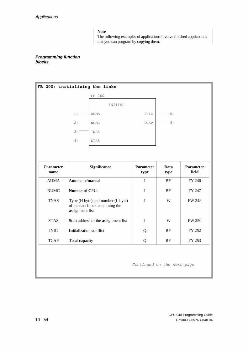
NoteThe following examples of applications involve finished applicationsthat you can program by copying them.
Programming functionblocks
FB 200: initializing the links
FB 200
INITIAL
(1) AUMA INIC (5)
(2) NUMC TCAP (6)
(3) TNAS
(4) STAS
Parametername
Significance Parametertype
Datatype
Parameterfield
AUMA
NUMC
TNAS
STAS
INIC
TCAP
Automatic/manual
Number of CPUs
Type (H byte) and number (L byte)of the data block containing theassignment list
Start address of the assignment list
Ini tialization conflict
Total capacity
I
I
I
I
Q
Q
BY
BY
W
W
BY
BY
FY 246
FY 247
FW 248
FW 250
FY 252
FY 253
Continued on the next page
Applications
CPU 948 Programming Guide
10 - 54 C79000-G8576-C848-04
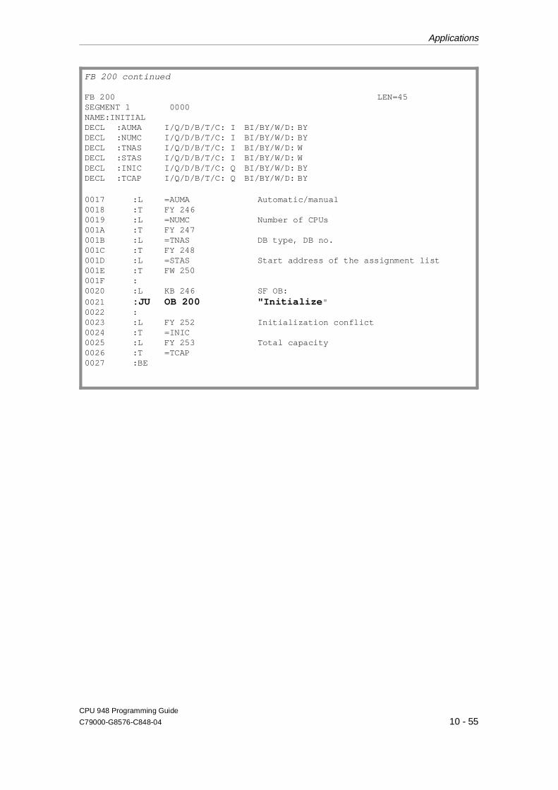
FB 200 continued
FB 200 LEN=45SEGMENT 1 0000NAME:INITIALDECL :AUMA I/Q/D/B/T/C: I BI/BY/W/D: BYDECL :NUMC I/Q/D/B/T/C: I BI/BY/W/D: BYDECL :TNAS I/Q/D/B/T/C: I BI/BY/W/D: WDECL :STAS I/Q/D/B/T/C: I BI/BY/W/D: WDECL :INIC I/Q/D/B/T/C: Q BI/BY/W/D: BYDECL :TCAP I/Q/D/B/T/C: Q BI/BY/W/D: BY
0017 :L =AUMA Automatic/manual0018 :T FY 2460019 :L =NUMC Number of CPUs001A :T FY 247001B :L =TNAS DB type, DB no.001C :T FY 248001D :L =STAS Start address of the assignment list001E :T FW 250001F :0020 :L KB 246 SF OB:0021 :JU OB 200 "Initialize "0022 :0023 :L FY 252 Initialization conflict0024 :T =INIC0025 :L FY 253 Total capacity0026 :T =TCAP0027 :BE
Applications
CPU 948 Programming Guide
C79000-G8576-C848-04 10 - 55
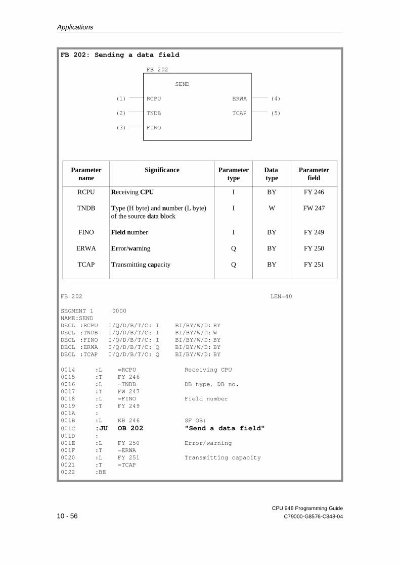
FB 202: Sending a data field
FB 202
SEND
(1) RCPU ERWA (4)
(2) TNDB TCAP (5)
(3) FINO
Parametername
Significance Parametertype
Data type
Parameterfield
RCPU
TNDB
FINO
ERWA
TCAP
Receiving CPU
Type (H byte) and number (L byte)of the source data block
Field number
Error/warning
Transmitting capacity
I
I
I
Q
Q
BY
W
BY
BY
BY
FY 246
FW 247
FY 249
FY 250
FY 251
FB 202 LEN=40
SEGMENT 1 0000NAME:SEND DECL :RCPU I/Q/D/B/T/C: I BI/BY/W/D: BYDECL :TNDB I/Q/D/B/T/C: I BI/BY/W/D: WDECL :FINO I/Q/D/B/T/C: I BI/BY/W/D: BYDECL :ERWA I/Q/D/B/T/C: Q BI/BY/W/D: BYDECL :TCAP I/Q/D/B/T/C: Q BI/BY/W/D: BY
0014 :L =RCPU Receiving CPU0015 :T FY 2460016 :L =TNDB DB type, DB no.0017 :T FW 2470018 :L =FINO Field number0019 :T FY 249001A :001B :L KB 246 SF OB:001C :JU OB 202 "Send a data field"001D :001E :L FY 250 Error/warning001F :T =ERWA0020 :L FY 251 Transmitting capacity0021 :T =TCAP0022 :BE
Applications
CPU 948 Programming Guide
10 - 56 C79000-G8576-C848-04
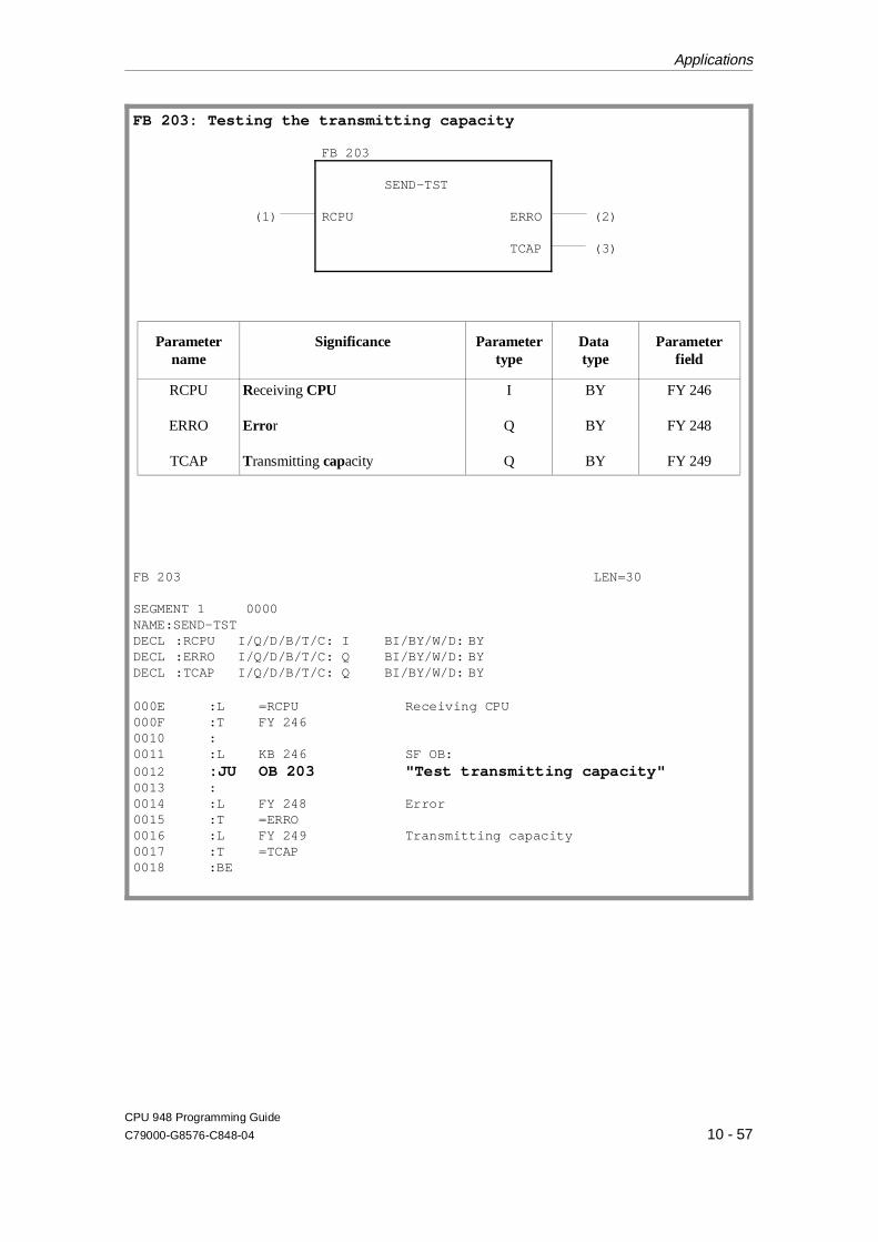
FB 203: Testing the transmitting capacity
FB 203
SEND-TST
(1) RCPU ERRO (2)
TCAP (3)
Parametername
Significance Parametertype
Data type
Parameterfield
RCPU
ERRO
TCAP
Receiving CPU
Erro r
Transmitting capacity
I
Q
Q
BY
BY
BY
FY 246
FY 248
FY 249
FB 203 LEN=30
SEGMENT 1 0000NAME:SEND-TSTDECL :RCPU I/Q/D/B/T/C: I BI/BY/W/D: BYDECL :ERRO I/Q/D/B/T/C: Q BI/BY/W/D: BYDECL :TCAP I/Q/D/B/T/C: Q BI/BY/W/D: BY
000E :L =RCPU Receiving CPU000F :T FY 2460010 :0011 :L KB 246 SF OB:0012 :JU OB 203 "Test transmitting capacity"0013 :0014 :L FY 248 Error0015 :T =ERRO0016 :L FY 249 Transmitting capacity0017 :T =TCAP0018 :BE
Applications
CPU 948 Programming Guide
C79000-G8576-C848-04 10 - 57
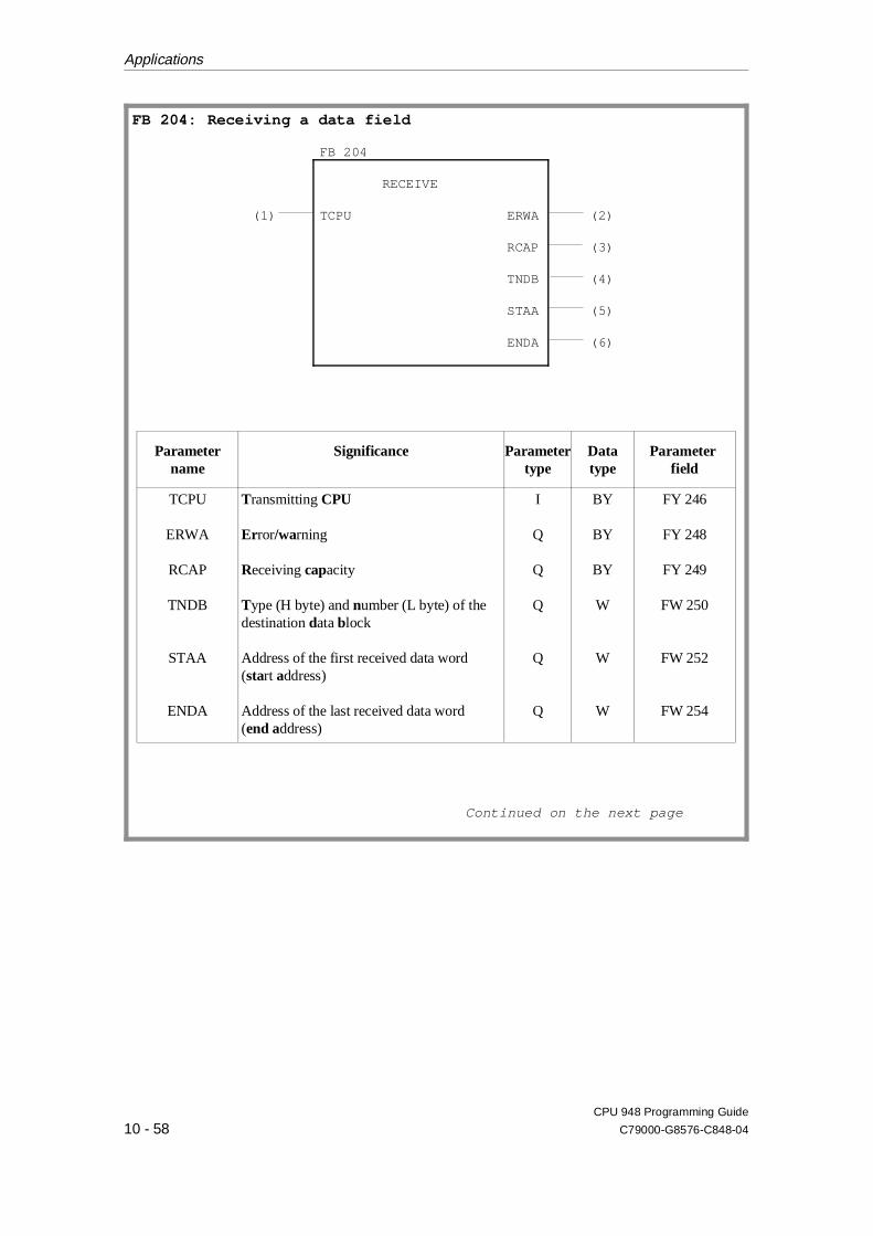
FB 204: Receiving a data field
FB 204
RECEIVE
(1) TCPU ERWA (2)
RCAP (3)
TNDB (4)
STAA (5)
ENDA (6)
Parametername
Significance Parametertype
Datatype
Parameter field
TCPU
ERWA
RCAP
TNDB
STAA
ENDA
Transmitting CPU
Error/warning
Receiving capacity
Type (H byte) and number (L byte) of thedestination data block
Address of the first received data word (start address)
Address of the last received data word (end address)
I
Q
Q
Q
Q
Q
BY
BY
BY
W
W
W
FY 246
FY 248
FY 249
FW 250
FW 252
FW 254
Continued on the next page
Applications
CPU 948 Programming Guide
10 - 58 C79000-G8576-C848-04

FB 204 continued:
FB 204 LEN=45
SEGMENT 1 0000NAME:RECEIVEDECL :TCPU I/Q/D/B/T/C: I BI/BY/W/D: BYDECL :ERWA I/Q/D/B/T/C: Q BI/BY/W/D: BYDECL :RCAP I/Q/D/B/T/C: Q BI/BY/W/D: BYDECL :TNDB I/Q/D/B/T/C: Q BI/BY/W/D: WDECL :STAA I/Q/D/B/T/C: Q BI/BY/W/D: WDECL :ENDA I/Q/D/B/T/C: Q BI/BY/W/D: W
0017 :L =TCPU Transmitting CPU0018 :T FY 2460019 :001A :L KB 246 SF OB:001B :JU OB 204 "Receive a data field"001C :001D :L FY 248 Error/warning001E :T =ERWA001F :L FY 249 Receiving capacity0020 :T =RCAP0021 :L FW 250 DB type, DB no.0022 :T =TNDB0023 :L FW 252 Start address0024 :T =STAA0025 :L FW 254 End address0026 :T =ENDA0027 :BE
FB 205: Testing the receiving capacity
FB 205
RECV-TST
(1) TCPU ERRO (2)
RCAP (3)
Parametername
Significance Parametertype
Datatype
Parameterfield
TCPU
ERRO
RCAP
Transmitting CPU
Erro r
Receiving capacity
I
Q
Q
BY
BY
BY
FY 246
FY 248
FY 249
Applications
CPU 948 Programming Guide
C79000-G8576-C848-04 10 - 59
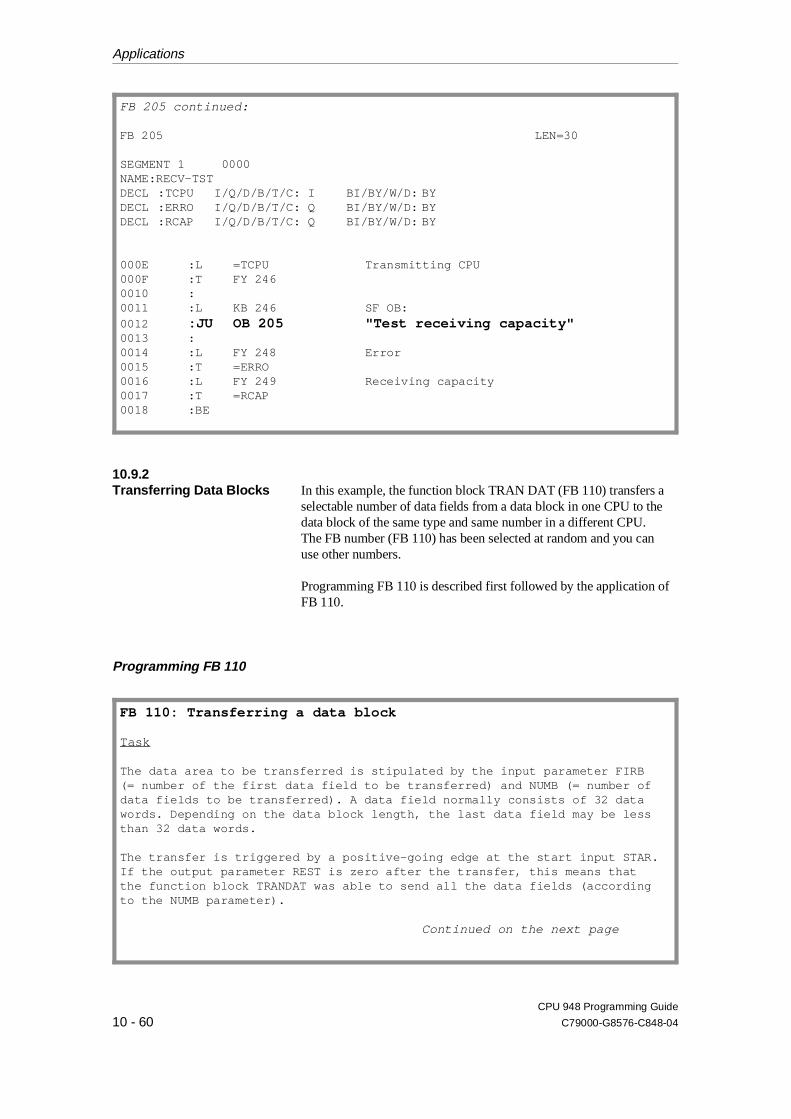
10.9.2Transferring Data Blocks In this example, the function block TRAN DAT (FB 110) transfers a
selectable number of data fields from a data block in one CPU to thedata block of the same type and same number in a different CPU. The FB number (FB 110) has been selected at random and you canuse other numbers.
Programming FB 110 is described first followed by the application ofFB 110.
Programming FB 110
FB 205 continued:
FB 205 LEN=30
SEGMENT 1 0000NAME:RECV-TSTDECL :TCPU I/Q/D/B/T/C: I BI/BY/W/D: BYDECL :ERRO I/Q/D/B/T/C: Q BI/BY/W/D: BYDECL :RCAP I/Q/D/B/T/C: Q BI/BY/W/D: BY
000E :L =TCPU Transmitting CPU000F :T FY 2460010 :0011 :L KB 246 SF OB:0012 :JU OB 205 "Test receiving capacity"0013 :0014 :L FY 248 Error0015 :T =ERRO0016 :L FY 249 Receiving capacity0017 :T =RCAP0018 :BE
FB 110: Transferring a data block
Task
The data area to be transferred is stipulated by the input parameter FIRB (= number of the first data field to be transferred) and NUMB (= number ofdata fields to be transferred). A data field normally consists of 32 datawords. Depending on the data block length, the last data field may be lessthan 32 data words.
The transfer is triggered by a positive-going edge at the start input STAR.If the output parameter REST is zero after the transfer, this means thatthe function block TRANDAT was able to send all the data fields (accordingto the NUMB parameter).
Continued on the next page
Applications
CPU 948 Programming Guide
10 - 60 C79000-G8576-C848-04

FB 110 continued:
If, however, the REST output parameter has a value greater than zero, thismeans that the function block must be called again, for example in the nextcycle. This means that you or the user program can only change the setparameters (i.e. the values of all parameters) when the REST parameterindicates zero showing that the data transfer is complete.
You can call the function block TRANDAT several times with differentparameters. In this case, various data areas are transferred simultaneously(interleaved in each other). The special function organization blocks formultiprocessor communication OB 202 to OB 205 can also be used "directly".This possibly is illustrated in the application example.
If the SEND function (OB 202) is not correctly executed with the TRANDATfunction block, the error number is entered in the output parameter ERRO, theRLO = ’1’ and the output parameter REST is set to ’0’.
The TRANDAT function block uses flag bytes FY 246 to FY 251 as scratchpadflags. All other variables whose value is significant as long as the outputparameter REST = ’0’ continue to have memory assigned to them using themechanism of formal/actual parameters. This is necessary to allow variousdata blocks to be transferred simultaneously.
Implementation
FB 110
TRAN-DAT
(1) STAR ERRO (6)
(2) RCPU REST (7)
(3) TNDB CUBN (8)
(4) NUMB EDGF (9)
(5) FIRB
Continued on the next page
Applications
CPU 948 Programming Guide
C79000-G8576-C848-04 10 - 61
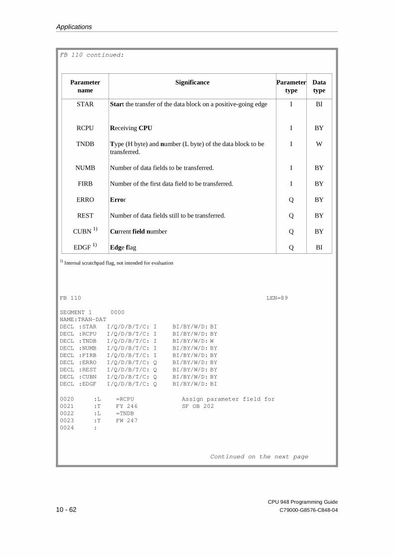
FB 110 continued:
Parametername
Significance Parametertype
Datatype
STAR
RCPU
TNDB
NUMB
FIRB
ERRO
REST
CUBN 1)
EDGF 1)
Start the transfer of the data block on a positive-going edge
Receiving CPU
Type (H byte) and number (L byte) of the data block to betransferred.
Number of data fields to be transferred.
Number of the first data field to be transferred.
Erro r
Number of data fields still to be transferred.
Current field number
Edge flag
I
I
I
I
I
Q
Q
Q
Q
BI
BY
W
BY
BY
BY
BY
BY
BI
1) Internal scratchpad flag, not intended for evaluation
FB 110 LEN=89
SEGMENT 1 0000NAME:TRAN-DATDECL :STAR I/Q/D/B/T/C: I BI/BY/W/D: BIDECL :RCPU I/Q/D/B/T/C: I BI/BY/W/D: BYDECL :TNDB I/Q/D/B/T/C: I BI/BY/W/D: WDECL :NUMB I/Q/D/B/T/C: I BI/BY/W/D: BYDECL :FIRB I/Q/D/B/T/C: I BI/BY/W/D: BYDECL :ERRO I/Q/D/B/T/C: Q BI/BY/W/D: BYDECL :REST I/Q/D/B/T/C: Q BI/BY/W/D: BYDECL :CUBN I/Q/D/B/T/C: Q BI/BY/W/D: BYDECL :EDGF I/Q/D/B/T/C: Q BI/BY/W/D: BI
0020 :L =RCPU Assign parameter field for0021 :T FY 246 SF OB 2020022 :L =TNDB0023 :T FW 2470024 :
Continued on the next page
Applications
CPU 948 Programming Guide
10 - 62 C79000-G8576-C848-04

FB 110 continued:
0025 :L =REST First send any remaining 0026 :L KB 0 data fields0027 :><F0028 :JC =TRAN0029 :002A :AN =STAR Positive edge at start002B :RB =EDGF input ?002C :ON =STAR002D :O =EDGF002E :JC =GOOD002F :S =EDGF0030 :0031 :L =NUMB Initialize the global flags0032 :T =REST after postive edge at0033 :L =FIRB START input0034 :T =CUBN0035 :0036 :L =REST As long as REST ><0, 0038 LOOP :L KF+0 continue to attempt to0039 :!=F send data fields003A :JC =GOOD003B TRAN :L =CUBN003C :T FY 249003D :L KB 246 SF OB:003E :JU OB 202 "Send a data field"003F :L FY 2500040 :JM =ERRO Abort if error0041 :JP =GOOD Abort if trans-cap. = 00042 :L =CUBN Increment0043 :I 1 field number0044 :T =CUBN0045 :L =REST Decrement number of0046 :D 1 remaining data fields0047 :T =REST0048 :JU =LOOP 0049 : 004A GOOD :A F 0.0 Regular end of program:004B :AN F 0.0004C :L KB 0 RLO = 0, ERRO = 0004D :T =ERRO004E :BE004F :0050 ERRO :T =ERRO Program end if error:0051 :L KB 00052 :T =REST RLO = 1, ERRO contains error number0053 :BE
Applications
CPU 948 Programming Guide
C79000-G8576-C848-04 10 - 63

Application of FB 110
Application of FB 110 on the S5-155U
Task
You want CPU 1 to transfer data blocks DB 3 ( data fields 2 to 5) and DB 4(data fields 1 to 3) to CPU 2 during the cyclic user program. The RECEIVEfunction (OB 204) is also called in the cyclic user program.
Implementation
Function CPU 1 CPU 2
called in: called in:
Initialization (OB 200)
Send organization (FB 1)
Receive organization (FB 2)
OB 20
OB 1
–
–
–
OB 1
exists: exists:
Send DB
Receive DB
DB 3; DB 4
–
–
DB 3; DB 4
The user program in function block FB 1 of CPU 1 contains two calls for thefunction block TRANDAT in each case with different sets of parameters.The transfer of the first data block DB 3 begins after a positive edgeafter input I 2.0. A positive edge at input I 2.1 starts the transfer ofthe second data block.
FB 1 LEN=yy
SEGMENT 1 0000NAME:S-ORG0000 :L KB 2 To CPU 2 ..0001 :T FY 00002 :L KY 1,3 .. from data block DB 30003 :T FW 10004 :L KB 4 .. four data fields0005 :T FY 30006 :L KB 2 .. send from 2nd data field0007 :T FY 40008 :
Continued on the next page
Applications
CPU 948 Programming Guide
10 - 64 C79000-G8576-C848-04
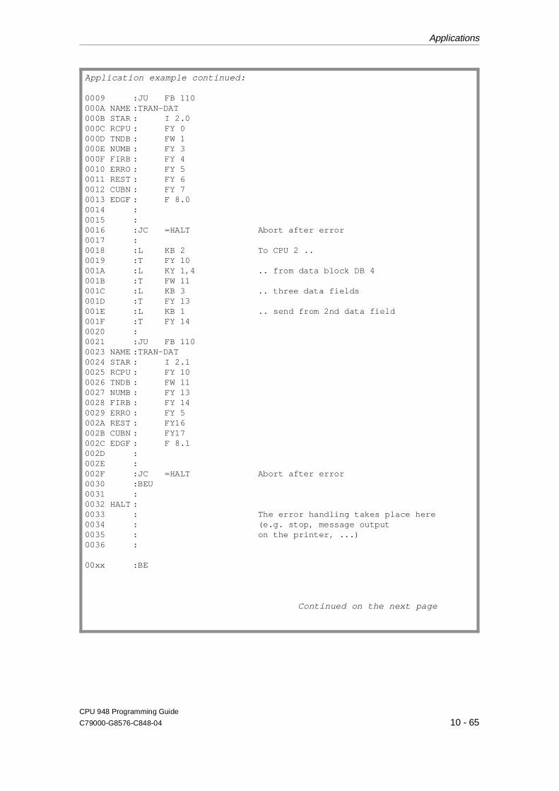
Application example continued:
0009 :JU FB 110000A NAME :TRAN-DAT000B STAR : I 2.0000C RCPU : FY 0000D TNDB : FW 1000E NUMB : FY 3000F FIRB : FY 40010 ERRO : FY 50011 REST : FY 60012 CUBN : FY 70013 EDGF : F 8.00014 :0015 :0016 :JC =HALT Abort after error0017 :0018 :L KB 2 To CPU 2 ..0019 :T FY 10001A :L KY 1,4 .. from data block DB 4001B :T FW 11001C :L KB 3 .. three data fields001D :T FY 13001E :L KB 1 .. send from 2nd data field001F :T FY 140020 :0021 :JU FB 1100023 NAME :TRAN-DAT0024 STAR : I 2.10025 RCPU : FY 100026 TNDB : FW 110027 NUMB : FY 130028 FIRB : FY 140029 ERRO : FY 5002A REST : FY16002B CUBN : FY17002C EDGF : F 8.1002D :002E :002F :JC =HALT Abort after error0030 :BEU0031 :0032 HALT :0033 : The error handling takes place here0034 : (e.g. stop, message output0035 : on the printer, ...)0036 :
00xx :BE
Continued on the next page
Applications
CPU 948 Programming Guide
C79000-G8576-C848-04 10 - 65
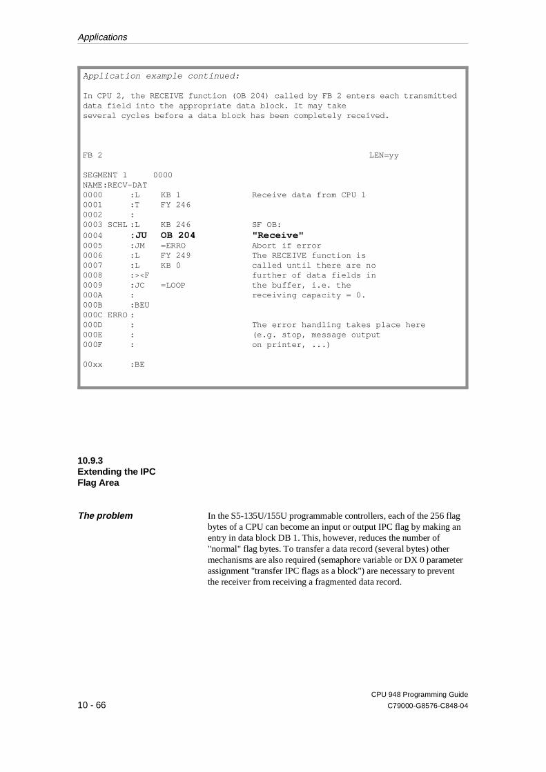
10.9.3Extending the IPCFlag Area
The problem In the S5-135U/155U programmable controllers, each of the 256 flagbytes of a CPU can become an input or output IPC flag by making anentry in data block DB 1. This, however, reduces the number of"normal" flag bytes. To transfer a data record (several bytes) othermechanisms are also required (semaphore variable or DX 0 parameterassignment "transfer IPC flags as a block") are necessary to preventthe receiver from receiving a fragmented data record.
Application example continued:
In CPU 2, the RECEIVE function (OB 204) called by FB 2 enters each transmitteddata field into the appropriate data block. It may take several cycles before a data block has been completely received.
FB 2 LEN=yy
SEGMENT 1 0000NAME:RECV-DAT0000 :L KB 1 Receive data from CPU 10001 :T FY 2460002 :0003 SCHL :L KB 246 SF OB:0004 :JU OB 204 "Receive"0005 :JM =ERRO Abort if error0006 :L FY 249 The RECEIVE function is 0007 :L KB 0 called until there are no 0008 :><F further of data fields in 0009 :JC =LOOP the buffer, i.e. the 000A : receiving capacity = 0.000B :BEU000C ERRO :000D : The error handling takes place here000E : (e.g. stop, message output 000F : on printer, ...)
00xx :BE
Applications
CPU 948 Programming Guide
10 - 66 C79000-G8576-C848-04
The solution Consecutive data words of a DB or DX data block are defined fromDW 0 onwards as "IPC data words". Each link is assigned its owndata block and is totally independent of the other links.
At the beginning of the cycle block, the IPC data words are received withthe aid of the special function organization blocks for multiprocessorcommunication. This is followed by the "regular" cyclic program, thatevaluates the received data and generates the data to be sent. At the endof the cycle, this data is then sent with the aid of the special organizationblocks for multiprocessor communication. It can therefore be received bythe other CPUs at the beginning of their cycles.
The following applies for each of the maximum 12 possible linksregardless of the other links:
•• The transmitting CPU is only active when the receiving CPU hasread out all the "old" data from the COR 923C buffer.
•• The receiving CPU is only active when the transmitting CPU haswritten all the "new" data in the COR 923C buffer.
This means that the receiving CPU can either receive a complete newdata record or the old data record remains unchanged: no mixing of"old" and "new" data.
Data structure Which data words (for the data word area below) are to be transferredfrom which CPU to which CPU is described in the link list (see the tableon the following page). This is located in an additional data block thatmust exist in all the CPUs involved.
The data word areas always begin from data word DW 0, and theirlengths are specified in data fields. Remember the following points:
•• A complete data field consists of 32 data words.
•• If the last data field is "truncated", i.e. it contains between 1 and 31data words, less data words are transferred.
•• If a send data block is longer than the number of fields of dataspecified in the link list, the excess data words can be used in thecorresponding CPU.
•• If a receive data block is longer than the received data word area,the excess data words can be used in the corresponding CPU.
Applications
CPU 948 Programming Guide
C79000-G8576-C848-04 10 - 67
Structure of thelink list
SUB-LIST 1 SUB-LIST 2
Link DB type DBnumber
No. of datafields
from CPU 1 to ...
DW 0 S 1 DW 16 S 1
... CPU 2 DW 1 ... ... DW 17 2 ...
... CPU 3 DW 2 ... ... DW 18 3 ...
...CPU 4 DW 3 ... ... DW 19 4 ...
from CPU 2to ...
DW 4 S 2 DW 20 S 2
... CPU 1 DW 5 ... ... DW 21 1 ...
... CPU 3 DW 6 1 1) 10 1) DW 22 3 2 1)
... CPU 4 DW 7 ... ... DW 23 4 ...
from CPU 3to ...
DW 8 S 3 DW 24 S 3
... CPU 1 DW 9 ... ... DW 25 1 ...
... CPU 2 DW 10 ... ... DW 26 2 ...
... CPU 4 DW 11 ... ... DW 27 4 ...
from CPU 4to ...
DW 12 S 4 DW 28 S 4
... CPU 1 DW 13 ... ... DW 29 1 ...
... CPU 2 DW 14 ... ... DW 30 2 ...
... CPU 3 DW 15 ... ... DW 31 3 ...
2 15 2 0 2 15 2 0
1) Refer to the example on the following page
Table 10-8 Link list for extending the IPC flag area
Applications
CPU 948 Programming Guide
10 - 68 C79000-G8576-C848-04
The link consists of two similarly structured sub-lists, each with 16 datawords. For each of the four sender CPUs (S1, S2, S3, S4) three entries arerequired to describe a link.
•• Number of data fields
The number of data fields specifies the size (= the number of datawords) of the data word area to be transferred. (If links do not existor you do not require them, enter 0 for the number of data fields,and for the DB type and DB number.)
•• DB type
Type of data block containing the data word area to be transferred.
•• DB number
Number of the data block containing the data word area to be trans-ferred.
As shown in the table, these entries can be read in and completed in lines.If, for example, you want to transfer the first two data fields in data blockDB 10 from CPU 2 (S2) to CPU 3, make the following entries:
CPU 2 (S 2) sends ..
Sub-list 2 is identical to the assignment ("manual" mode) required forthe INITIALIZE function (OB 200). Within the data block, sub-list 2must occupy data words 0 to 15 and sub-list 2 data words 16 to 31.You must not alter the entries shown in bold face.
DW 22 3 2 DW 6 1 10
..to CPU 3 2 data fields from DB 10
Applications
CPU 948 Programming Guide
C79000-G8576-C848-04 10 - 69

Program structure During restart, one of the CPUs calls the INITIALIZE function (OB200) to reserve exactly the same number of coordinator memory fieldsper link as data fields to be transmitted on this link.
To send and receive data word areas, each CPU uses two functionblocks:
FB no. Name Function
FB 100
FB 101
SEND-DAT
RECV-DAT
Send data word areasto the other CPUs
Receive data word areas from the other CPUs
These FB numbers have been selected at random and you can useothers.
The function blocks SEND-DAT and RECV-DAT read the link list todetermine which data word areas are to be sent from or received by whichdata blocks. The whole data word area is always sent or received. If thisis not possible owing to insufficient transmitting or receiving capacity, thesend or receive function is not executed.
NoteThis example (IPC flag extension using function blocksSEND-DAT and RECV-DAT) can only run correctly when thespecial function organization blocks for multiprocessorcommunication OB 202 to OB 205 are not called in any of theCPUs.
The function blocks SEND-DAT and RECV-DAT contain thespecial function organization blocks for multiprocessorcommunication OB 202 to OB 205. You cannot call theseorganization blocks outside SEND-DAT/RECV-DAT.
Applications
CPU 948 Programming Guide
10 - 70 C79000-G8576-C848-04

OB 20
Restart OB to reservethe buffer on the923C coordinator JU OB 200
BE
Cycl ic user programextended by the cal ls forthe RECV-DAT and SEND-DATfunct ion blocks.
OB 1
CJU
DB xxxFB 101
CJU
DB xxxFB 100
BE
FB 100
FB 101
Funct ion block: SEND-DATSend data blocks
Funct ion block: RECV-DATReceive data blocks
Data block containingthe l ink l is t
Maximum three input andthree output blocks
DB xxx
BE
BE
KS = S1KY = 1,. . . evalu-
ated
by .. .
DB yyyor/andDX zzz
.
.
.
.
.
.
.
.
.
.
.
.
OB 200 mustonly be cal ledin one processor.
1)
1)
Fig. 10-6 Overview of the blocks required in each CPU
Applications
CPU 948 Programming Guide
C79000-G8576-C848-04 10 - 71
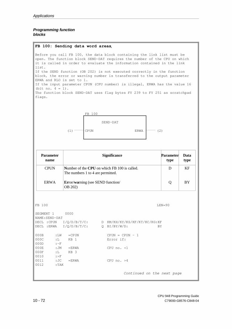
Programming functionblocks
FB 100: Sending data word areas
Before you call FB 100, the data block containing the link list must beopen. The function block SEND-DAT requires the number of the CPU on whichit is called in order to evaluate the information contained in the linklist. If the SEND function (OB 202) is not executed correctly in the functionblock, the error or warning number is transferred to the output parameterERWA and RLO is set to 1.If the input parameter CPUN (CPU number) is illegal, ERWA has the value 16(bit no. 4 = 1).The function block SEND-DAT uses flag bytes FY 239 to FY 251 as scratchpadflags.
FB 100
SEND-DAT
(1) CPUN ERWA (2)
Parametername
Significance Parametertype
Datatype
CPUN
ERWA
Number of the CPU on which FB 100 is called.The numbers 1 to 4 are permitted.
Error/warning (see SEND function/OB 202)
D
Q
KF
BY
FB 100 LEN=90
SEGMENT 1 0000NAME:SEND-DATDECL :CPUN I/Q/D/B/T/C: D KM/KH/KY/KS/KF/KT/KC/KG:KFDECL :ERWA I/Q/D/B/T/C: Q BI/BY/W/D: BY
000B :LW =CPUN CPUN = CPUN - 1000C :L KB 1 Error if:000D :-F000E :JM =ERWA CPU no. <1000F :L KB 30010 :>F0011 :JC =ERWA CPU no. >40012 :TAK
Continued on the next page
Applications
CPU 948 Programming Guide
10 - 72 C79000-G8576-C848-04

FB 100 continued:
0013 :0014 :SLW 2 CPUN = CPUN * 40015 :T FY 245 Base address0016 :0017 :L KB 10018 :T FY 244 Link counter0019 :001A LOOP :L FY 245 Base address001B :L FY 244 + counter001C :+F001D :T FW 240001E :ADD BN+16 + offset001F :T FW 2420020 :0021 :DO FW 2420022 :L DR 0 Number of reserved0023 :T FY 239 fields = 0 ?0024 :L KB 00025 :!=F0026 :JC =EMPT0027 :0028 :B FW 2420029 :L DL 0 No. of the receiving CPU002A :T FY 246002B :L KB 246 SF OB:002C :JU OB 203 "Test sending capacity"002D :L FY 248 Abort if error002E :JC =OBER002F :0030 :L FY 249 Transmitting capacity >< no.0031 :L FY 239 of reserved fields?0032 :><F0033 :JC =EMPT0034 :0035 :L KB 0 Field counter0036 :T FY 2490037 :0038 :B FY 2400039 :L DW 0 Type and number of 003A :T FW 247 the source DB003B :003C TRAN :L KB 246 SF OB:003D :JU OB 202 Send a data field003E :L FY 250 Abort if error/warning003F :JC =OBER0040 :0041 :L FY 249 Field no. = field no. + 10042 :I 10043 :T FY 249 All data fields transferred?0044 :L FY 2390045 :<F0046 :JC =TRAN0047 :
Continued on the next page
Applications
CPU 948 Programming Guide
C79000-G8576-C848-04 10 - 73
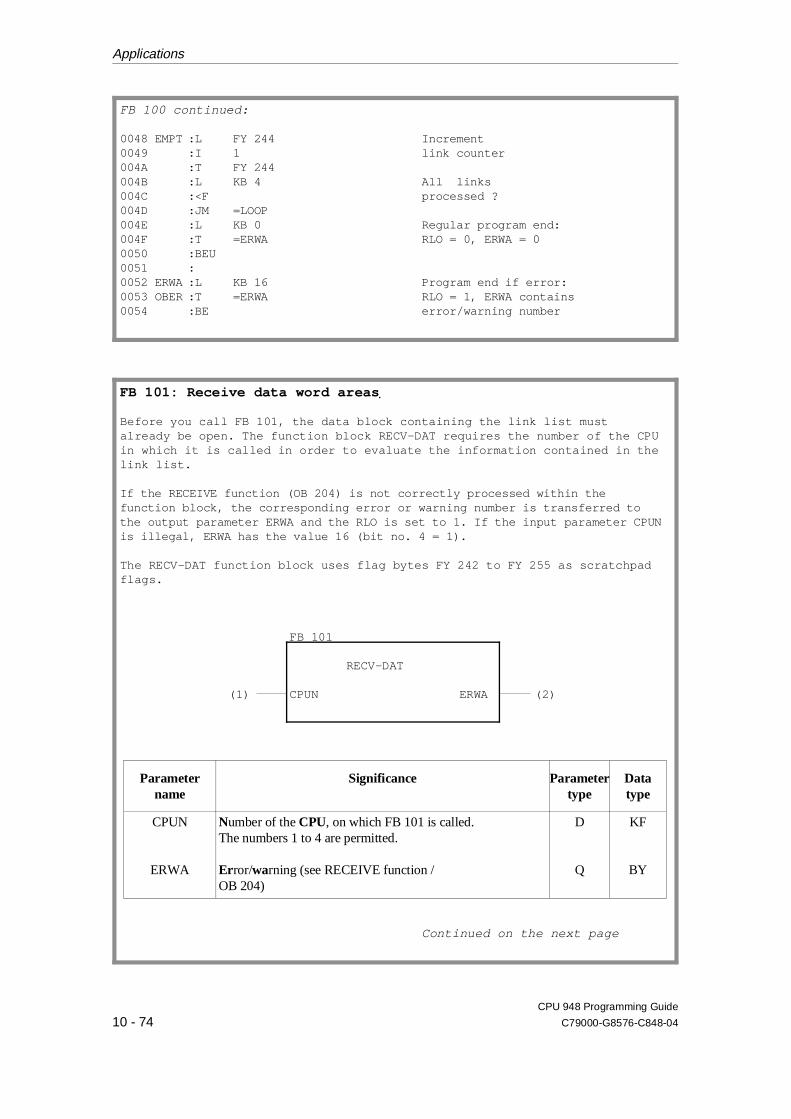
FB 100 continued:
0048 EMPT :L FY 244 Increment0049 :I 1 link counter004A :T FY 244004B :L KB 4 All links004C :<F processed ?004D :JM =LOOP004E :L KB 0 Regular program end:004F :T =ERWA RLO = 0, ERWA = 00050 :BEU0051 :0052 ERWA :L KB 16 Program end if error:0053 OBER :T =ERWA RLO = 1, ERWA contains0054 :BE error/warning number
FB 101: Receive data word areas
Before you call FB 101, the data block containing the link list mustalready be open. The function block RECV-DAT requires the number of the CPUin which it is called in order to evaluate the information contained in thelink list.
If the RECEIVE function (OB 204) is not correctly processed within thefunction block, the corresponding error or warning number is transferred tothe output parameter ERWA and the RLO is set to 1. If the input parameter CPUNis illegal, ERWA has the value 16 (bit no. 4 = 1).
The RECV-DAT function block uses flag bytes FY 242 to FY 255 as scratchpadflags.
FB 101
RECV-DAT
(1) CPUN ERWA (2)
Parametername
Significance Parametertype
Datatype
CPUN
ERWA
Number of the CPU, on which FB 101 is called. The numbers 1 to 4 are permitted.
Er ror/warning (see RECEIVE function /OB 204)
D
Q
KF
BY
Continued on the next page
Applications
CPU 948 Programming Guide
10 - 74 C79000-G8576-C848-04

FB 101 continued:
FB 101 LEN=88
SEGMENT 1 0000NAME:RECV-DATDECL :CPUN I/Q/D/B/T/C: D KM/KH/KY/KS/KF/KT/KC/KG: KFDECL :ERWA I/Q/D/B/T/C: Q BI/BY/W/D: BY
000B :LW =CPUN Error if:000C :L KB 1000D :<F000E :JC =ERWA CPU no. <1000F :LW =CPUN0010 :L KB 40011 :>F0012 :JC =ERWA CPU no. >40013 :0014 :L KB 1 Link counter0015 :T FY 2420016 :0017 :L KB 160018 :T FW 244 Pointer to sub-list 20019 :001A SRCH :L FW 244 Search sub-list 2 until001B :I 1 the next entry for the001C :T FW 244 receiving CPU with the001D :DO FW 244 number ’CPUN’ is found.001E :L DL 0001F :LW =CPUN0020 :><F0021 :JC =SRCH0022 :0023 :DO FW 2440024 :L DR 0 Number of reserved0025 :T FY 243 memory fields = 0 ?0026 :L KB 00027 :!=F0028 :JC =EMPT0029 :002A :L FW 244 Determine the number of the002B :L KM 00000000 00001100 transmitting CPU from the002D :AW pointer to sub-list 2.002E :SRW 2002F :I 10030 :T FY 2460031 :0032 :L KB 246 SF OB:0033 :JU OB 205 "Test receiving capacity" 0034 :L FY 2480035 :JC = OBER Abort if error0036 :
Continued on the next page
Applications
CPU 948 Programming Guide
C79000-G8576-C848-04 10 - 75
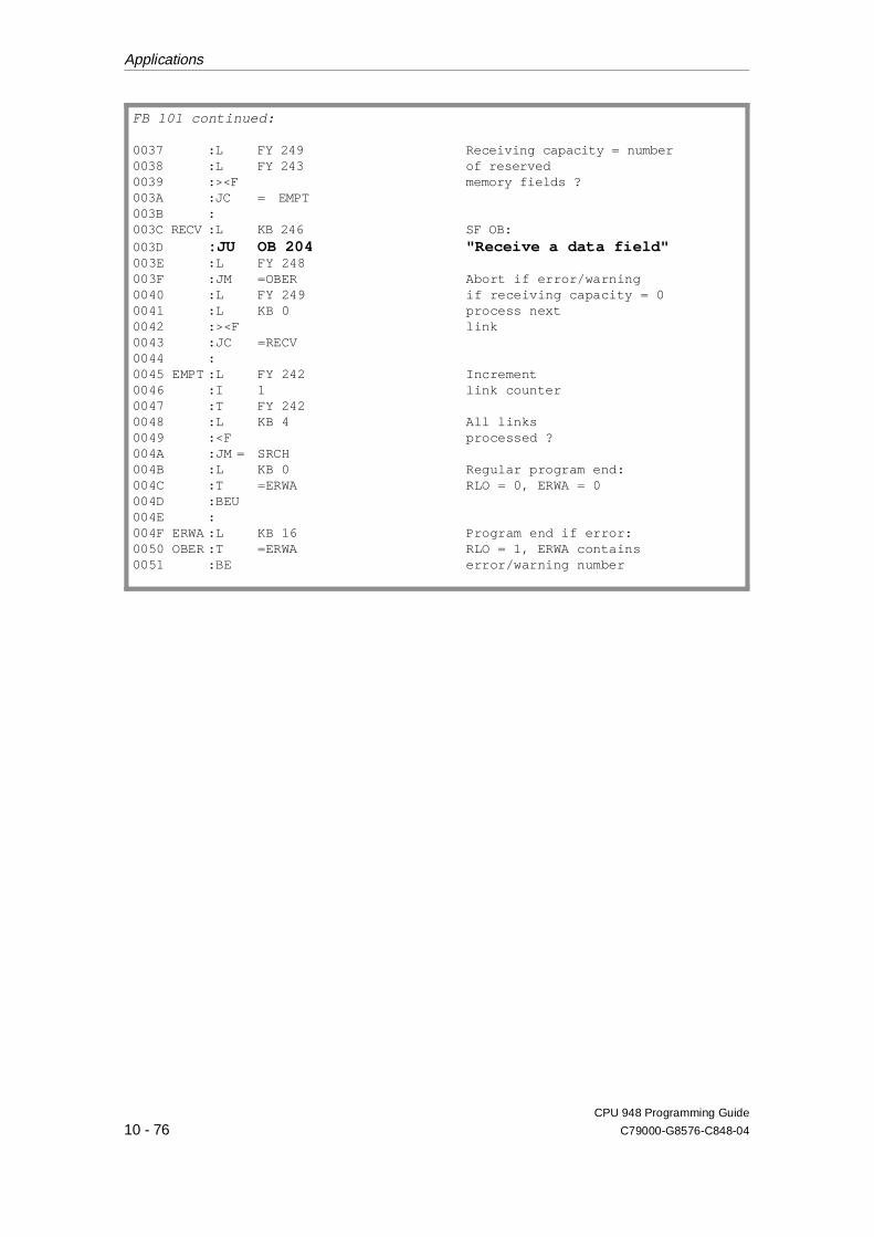
FB 101 continued:
0037 :L FY 249 Receiving capacity = number 0038 :L FY 243 of reserved0039 :><F memory fields ?003A :JC = EMPT003B :003C RECV :L KB 246 SF OB:003D :JU OB 204 "Receive a data field"003E :L FY 248003F :JM =OBER Abort if error/warning 0040 :L FY 249 if receiving capacity = 00041 :L KB 0 process next0042 :><F link0043 :JC =RECV0044 :0045 EMPT :L FY 242 Increment0046 :I 1 link counter0047 :T FY 2420048 :L KB 4 All links0049 :<F processed ?004A :JM = SRCH004B :L KB 0 Regular program end:004C :T =ERWA RLO = 0, ERWA = 0004D :BEU004E :004F ERWA :L KB 16 Program end if error:0050 OBER :T =ERWA RLO = 1, ERWA contains0051 :BE error/warning number
Applications
CPU 948 Programming Guide
10 - 76 C79000-G8576-C848-04

Application example
Application of FB 100/101 on the S5-155U
Task
You want to exchange data between three CPUs:
- From CPU 1 to CPU 2: data block DB 3, DW 0 to DW 127 (= 4 data fields)
- From CPU 1 to CPU 3: data block DX 4, DW 0 to DW 63 (= 2 data fields)
- From CPU 2 to CPU 1 and CPU 3: data block DB 5, DW 0 to DW 95 (= 3 data fields)
Function block FB 1 is the interface for the cyclic user program on allthree CPUs. CPU 1 calls the INITIALIZE function (OB 200) during the coldrestart. The link list is in data block DB 100.
Continued on the next page
DB 5, 3 data f ie lds
DB 3,4 dataf ie lds
DB 5,3 dataf ie lds
DX 4, 2 data f ie lds
CPU 2 CPU 3
CPU 1
Fig. 10-7 Data exchange between 3 CPUs
Applications
CPU 948 Programming Guide
C79000-G8576-C848-04 10 - 77
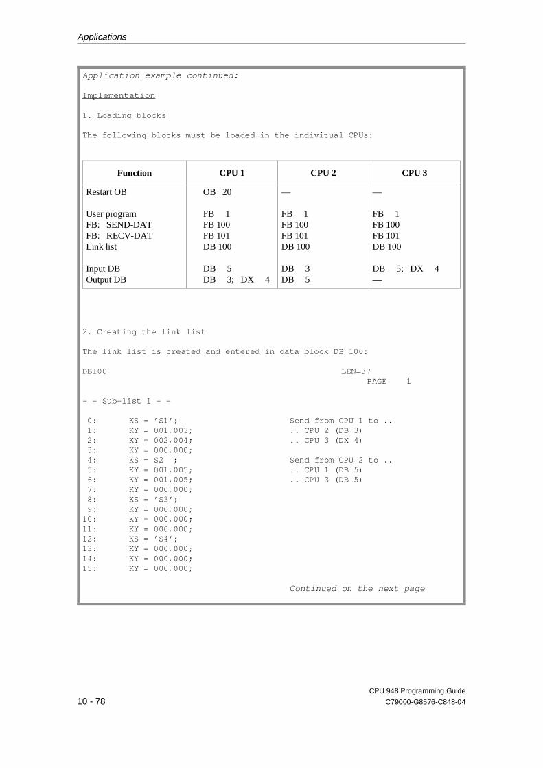
Application example continued:
Implementation
1. Loading blocks
The following blocks must be loaded in the indivitual CPUs:
Function CPU 1 CPU 2 CPU 3
Restart OB
User programFB: SEND-DATFB: RECV-DATLink list
Input DBOutput DB
OB 20
FB 1FB 100FB 101DB 100
DB 5DB 3; DX 4
—
FB 1FB 100FB 101DB 100
DB 3DB 5
—
FB 1FB 100FB 101DB 100
DB 5; DX 4—
2. Creating the link list
The link list is created and entered in data block DB 100:
DB100 LEN=37PAGE 1
– – Sub-list 1 – –
0: KS = ’S1’; Send from CPU 1 to .. 1: KY = 001,003; .. CPU 2 (DB 3) 2: KY = 002,004; .. CPU 3 (DX 4) 3: KY = 000,000; 4: KS = S2 ; Send from CPU 2 to .. 5: KY = 001,005; .. CPU 1 (DB 5) 6: KY = 001,005; .. CPU 3 (DB 5) 7: KY = 000,000; 8: KS = ’S3’; 9: KY = 000,000;10: KY = 000,000;11: KY = 000,000;12: KS = ’S4’;13: KY = 000,000;14: KY = 000,000;15: KY = 000,000;
Continued on the next page
Applications
CPU 948 Programming Guide
10 - 78 C79000-G8576-C848-04

Application example continued:
– – Sub-list 1 – –
16: KS = ’S1’; Send from CPU 1 to ..17: KY = 002,004; .. CPU 2 (four data fields)18: KY = 003,002; .. CPU 3 (two data fields)19: KY = 004,000;20: KS = S2’; Send from CPU 2 to ..21: KY = 001,003; .. CPU 1 (three data fields)22: KY = 003,003; .. CPU 3 (three data fields)23: KY = 004,000;24: KS = ’S3’;25: KY = 001,000;26: KY = 002,000;27: KY = 004,000;28: KS = ’S4’;29: KY = 001,000;30: KY = 002,000;31: KY = 003,000;
Data words DW 16 to DW 31 contain the assignment list required for themanual INITIALIZATION function (OB 200).
3. Program OB 200 call in the start-up block OB 20 for CPU 1
OB 200 is called by the OB 20 shown below in CPU 1 during the restart.
OB 20 LEN=yyABS
SEGMENT 10000 :L KB 2 Manual initialization of0001 :T FY 246 the pages0002 :0003 :L KY 1,100 The assignment list is entered0005 :T FW 248 in DB 100 from data word 160006 :L KF+16 onwards0008 :T FW 2500009 :000A :L KB 246 SF OB:000B :JU OB 200 "Initialize"000C :000D :AN F 252.5 Block end if there is no000E :BEC initialization conflict000F :0010 : The error handling routine 0011 : is inserted here if an0012 : initialization clonflict 0013 : occurs (e.g. stop, output 0014 : message on printer, or ...)
00xx :BE
Continued on the next page
Applications
CPU 948 Programming Guide
C79000-G8576-C848-04 10 - 79
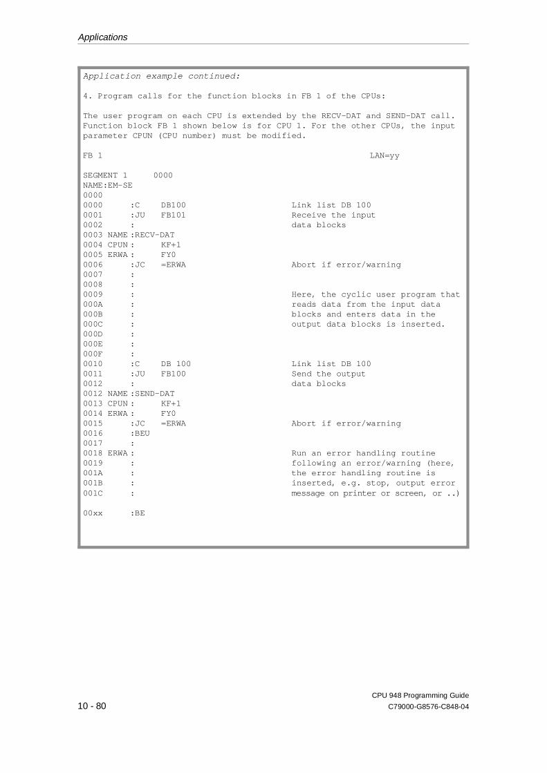
Application example continued:
4. Program calls for the function blocks in FB 1 of the CPUs:
The user program on each CPU is extended by the RECV-DAT and SEND-DAT call.Function block FB 1 shown below is for CPU 1. For the other CPUs, the inputparameter CPUN (CPU number) must be modified.
FB 1 LAN=yy
SEGMENT 1 0000NAME:EM-SE00000000 :C DB100 Link list DB 1000001 :JU FB101 Receive the input0002 : data blocks0003 NAME :RECV-DAT0004 CPUN : KF+10005 ERWA : FY00006 :JC =ERWA Abort if error/warning0007 :0008 :0009 : Here, the cyclic user program that000A : reads data from the input data 000B : blocks and enters data in the 000C : output data blocks is inserted.000D :000E :000F :0010 :C DB 100 Link list DB 1000011 :JU FB100 Send the output0012 : data blocks0012 NAME :SEND-DAT0013 CPUN : KF+10014 ERWA : FY00015 :JC =ERWA Abort if error/warning0016 :BEU0017 :0018 ERWA : Run an error handling routine0019 : following an error/warning (here,001A : the error handling routine is001B : inserted, e.g. stop, output error001C : message on printer or screen, or ..)
00xx :BE
Applications
CPU 948 Programming Guide
10 - 80 C79000-G8576-C848-04
Contents of Chapter 11
11.1 Overview. . . . . . . . . . . . . . . . . . . . . . . . . . . . . . . . . . . . . . . . . . . . . . . . . . . . . . . . . . . . . . 11 - 4
11.2 PG Functions. . . . . . . . . . . . . . . . . . . . . . . . . . . . . . . . . . . . . . . . . . . . . . . . . . . . . . . . . . . 11 - 5
11.2.1 Info . . . . . . . . . . . . . . . . . . . . . . . . . . . . . . . . . . . . . . . . . . . . . . . . . . . . . . . . . . . . . . . . . . 11 - 611.2.2 Installation. . . . . . . . . . . . . . . . . . . . . . . . . . . . . . . . . . . . . . . . . . . . . . . . . . . . . . . . . . . . . 11 - 711.2.3 Program Test . . . . . . . . . . . . . . . . . . . . . . . . . . . . . . . . . . . . . . . . . . . . . . . . . . . . . . . . . . . 11 - 8
11.3 Serial Link PG - PLC via 1st or 2nd Serial Interface . . . . . . . . . . . . . . . . . . . . . . . . . . 11 - 16
11.4 Parallel Operation of Two Serial PG Interfaces . . . . . . . . . . . . . . . . . . . . . . . . . . . . . . 11 - 17
11.4.1 Installation. . . . . . . . . . . . . . . . . . . . . . . . . . . . . . . . . . . . . . . . . . . . . . . . . . . . . . . . . . . . 11 - 1911.4.2 Operation. . . . . . . . . . . . . . . . . . . . . . . . . . . . . . . . . . . . . . . . . . . . . . . . . . . . . . . . . . . . . 11 - 1911.4.3 Sequence in Certain Operating Situations . . . . . . . . . . . . . . . . . . . . . . . . . . . . . . . . . . . 11 - 21
11.5 PG Functions via the S5 Bus . . . . . . . . . . . . . . . . . . . . . . . . . . . . . . . . . . . . . . . . . . . . . 11 - 27
11.5.1 Application . . . . . . . . . . . . . . . . . . . . . . . . . . . . . . . . . . . . . . . . . . . . . . . . . . . . . . . . . . . 11 - 2711.5.2 How the PG Functions Work via the S5 Bus . . . . . . . . . . . . . . . . . . . . . . . . . . . . . . . . 11 - 2911.5.3 Installation and Getting Started . . . . . . . . . . . . . . . . . . . . . . . . . . . . . . . . . . . . . . . . . . . 11 - 3111.5.4 Condition Codes Indicating Problems . . . . . . . . . . . . . . . . . . . . . . . . . . . . . . . . . . . . . . 11 - 35
PG Interfaces and Functions 11
CPU 948 Programming Guide
C79000-G8576-C848-04 11 - 1

Contents
CPU 948 Programming Guide
11 - 2 C79000-G8576-C848-04
11PG Interfaces and Functions
This chapter explains how to connect your PG to the CPU 948 and thefunctions provided by the PG software with which you can test yourSTEP 5 program.If you only use the standard PG interface (1st serial PG interface) youdo not need to read Sections 11.4 and 11.5. These sections tell youabout further interfaces with which you can connect a PG to yourCPU. These sections also contain points to note if you use PGfunctions on both interfaces.
CPU 948 Programming Guide
C79000-G8576-C848-04 11 - 3
11.1 Overview
You can load and test your user program using the online functions ofthe STEP 5 software.
To use these functions, the CPU must be connected to the PG. Thefollowing interfaces are available for this link:
•• link via the serial standard interface "PG - PLC",
•• link via the 2nd serial interface of the CPU 948,
•• link via the S5 bus with SINEC H1.
The PG functions can operate simultaneously on the two serialinterfaces, however, via the SINEC H1 link, the PG functions can onlybe used alternately with those on the serial interfaces
PG functions provide the following support for installing and testingyour STEP 5 program:
Function Section
Info
Size of the internal RAM and freeuser memory
"Memory configuration"
List of loaded blocks "Output DIR"
Display contents of memorywords/bytes and I/O bytes
"Output address"
Memory management
Delete the whole memory "Overall reset"
Create more memory space "Compress memory
Manage blocks "Transfer/delete blocks"
Program test
Start/stop CPU "Start/stop"
Test the operation sequence in ablock
"Status block"
Test single program steps "Program test"
Display signal state of processvariables
"Status variables"
Output signals in the stop mode "Force"
Display/change process variables "Force variables"
Table 11-1 Functions for installation and testing
Overview
CPU 948 Programming Guide
11 - 4 C79000-G8576-C848-04
11.2 PG Functions
NoteThe terms used in this section for the PG functions may in somecases differ from the terms in your PG software. Please refer toyour STEP 5 manual.
Calling and using functions How to call and use the individual PG functions is described in themanual for your PG.
Checkpoint The PG functions are performed at defined checkpoints in the CPU.In the CPU 948 there are four different checkpoints. Each of thesecheckpoints has certain test functions assigned to it.
Checkpoint "Stop"
You can access PG functions that are permissible only in the STOPmode at checkpoint "stop" (e.g. "start", "overall reset", "compressmemory" in the stop mode). The "stop" checkpoint is located immediately before OB 39 is called(the block for cyclic processing in the soft STOP mode).
Checkpoint "Cycle"
PG functions that you want to execute during cyclic programprocessing are called at checkpoint "cycle" (e.g. "compress memory"in the RUN mode, "stop", "status"). The "cycle" checkpoint is locatedimmediately before the updating of the process image of the inputs(PII). At this point, the system program has not updated the PII yet.
Checkpoint "Test"
PG functions that you want to execute as soon as the next breakpointis reached are called at checkpoint "test" (in the program test), seeSection 11.2.3).
Checkpoint "General Functions"
This checkpoint exists both in the STOP and the RUN mode. OnlinePG functions that can be executed in all operating modes of theprogrammable controller are called at checkpoint "general functions".These functions include "transfer block", "delete block", "statusvariables". In the STOP mode, this checkpoint is located immediatelybefore OB 39 is called (the block for cyclic processing in the softSTOP mode). During cyclic program processing, the checkpoint islocated after updating the process image of the inputs and beforecalling OB 1.
PG Functions
CPU 948 Programming Guide
C79000-G8576-C848-04 11 - 5

11.2.1Info
Memory configuration The CPU 948 is available with two memory versions and you cancheck the memory capacity using the PG function "memoryconfiguration". With this function, the following information aboutthe CPU user memory is transferred to the PG (from PG softwareversion V6.0 upwards with "Delta diskette" for the CPU 948):
•• memory capacity (640 Kbytes/1664 Kbytes)
•• longest free block of user memory
•• sum of all free blocks of user memory.
The PG software V6.3 with "Delta diskette" for the CPU 948 displaysthe memory configuration exactly.With older PG software versions (e.g. V3.0 or MT1.0) the memoryconfiguration is as for the CPU 946/947 (refer to Fig. 11-1). The totalmemory configuration of the CPU 948 must then be calculated fromthe total of the submodule values.
P L C i n f o SIMATIC S5 / OES0C
M e m o r y configuration S 5 1 5 5 U
Module Submod Type Start address End address Length
0 1
1
2
2
2
2
2
3
3
Longest free block of RAM
Sum of all free blocks of RAM
1
1
1
1
RAM
RAM
RAM
00000
10000
30000
Submod. empty / not plugged in
Submod. empty / not plugged in
Submod. empty / not plugged in
Submod. empty / not plugged in
0FFFF
2FFFF
4FFFF
64 KW
1)
1) corresponds to the memory configuration of the CPU 948-1: 320 Kw = 640 Kbytes
128 KW
128 KW
: 314800 Words
: 315664 Words
F1 F2 F3 F4 F5 F6OUTP ADDR MEM CONF SYSPAR BSTACK ISTACK RETURN
F7 F8
Fig. 11-1 PG display of the memory configuration
PG Functions
CPU 948 Programming Guide
11 - 6 C79000-G8576-C848-04

Output DIR If you want to display a list of all the programmed blocks on the PGwith the CPU 948, OB 0 is displayed instead of the system programblocks.
The function is permitted in the operating modes RUN, SOFT STOP,HARD STOP and can also be called within the "program test"function.
Output address With the "output address" function, you can display the contents ofmemory and I/O addresses in hexadecimal format. You can access alladdresses (RAM, S5 bus, areas with no modules assigned). In theprocess image area no ADF is triggered, in the I/O area there is noQVZ.
In the areas addressed as bytes (flags, process image) the high byte isrepresented as ’FF’.
11.2.2Installation
Overall reset With the function "delete all blocks" you can carry out an overall resetof the CPU from the PG. The overall reset is carried outunconditionally (refer to Section 4.2).
Compress memory This function shifts all valid blocks in the user memory to thebeginning of the user memory. Unused areas that resulted fromdeleting or correcting blocks are eliminated. This function shiftscomplete blocks to the beginning of the memory area. Ideally, onelarge free area results from many small unused areas. You can loadblocks into the resulting large space.
You can call this function in the RUN and soft STOP modes. In theRUN mode, DBs and DXs that are longer than 512 data words are notshifted. In the STOP mode, all blocks are shifted.
The blocks are shifted via a buffer so that no data is lost if there is apower failure. If this buffer is insufficient for intermediate storage of ablock, compressing continues at the next unused memory area.Consequently, some unused areas can still remain after compressing.
See also Section 8.3.
PG Functions
CPU 948 Programming Guide
C79000-G8576-C848-04 11 - 7
Transfer block With this function you can transfer new or existing logic and datablocks to the user memory of the CPU.
If a block already exists in the user memory of the CPU, it is declaredinvalid and the new block becomes valid.
Delete block With this function you declare a logic or data block in the usermemory as invalid.
The space taken up by such blocks is released and can be used again.
11.2.3Program Test
Start/stop When you use the START and STOP PG functions, operating the PGcorresponds to manual operation.
You can put the programmable controller into the STOP mode bycalling the STOP function while the controller is in the RUN mode.
PGSTP is marked in the control bit display. In multiprocessoroperation, the HALT control bit is set for the other CPUs.
You exit the SOFT STOP status with a COLD RESTART or WARMRESTART. In the single processor mode, the CPU exits the stopmode. In multiprocessor operation, the restart type is registeredinitially (the NEUDF or WIEDF control bit is set). However, the CPUstays in the soft STOP mode until all CPUs are initialized formultiprocessing. With the next operation "system start" you can startthe programmable controller. This corresponds to switching thecoordinator switch to RUN.
You can call the START PG function in the multiprocessor mode toselect the restart type you want for all the CPUs you are using. Afterthat, you can start the programmable controller with the last CPU.
PG Functions
CPU 948 Programming Guide
11 - 8 C79000-G8576-C848-04
Status block You can call the "status" PG function to test related operationalsequences (STEP 5 operations) in one block at any location in the userprogram. The current signal status of operands, the accumulator contents, andthe RLO are output on the PG screen for every executed operation inthe block (i.e., step mode). You can also use this function to test theparameter assignment of function blocks (i.e., field operation): The signal status of the actual operands is displayed.
Calling the function andspecifying a breakpoint
When you call the "status" function on a PG and enter the type andnumber of the block you want to test (possibly including the nestingsequence and search key), you enter a breakpoint.
When the "status" function is called during program processing in theRUN mode, program processing continues until it reaches theoperation marked by the specified breakpoint in the correct nestingsequence. Then the system program executes each of the monitoredoperations up to the operation boundary, outputting the processingresults to the PG.
NoteThe results of operation processing are not output in each of thesubsequent cycles.
Nesting and interruptions A sequence of operations marked by a breakpoint is completed even ifa different program execution level (e.g., an error OB or interrupt OB)is activated and processed. With this you can see whether data hasbeen changed by nested program sections.
If an interruption in a nested program execution level puts the CPUinto the STOP mode, data is output up to the operation that wasexecuted before the program execution levels changed. The data of theremaining operations is padded with zeros (the SAC is also 0).
The "status" function is possible in the following modes. RUN,RESTART (OB 20, OB 21, OB 22) soft STOP (OB 39 only).
DO FW/DO DW operations While the "status block" function is active, if the cursor is positionedexactly on the operation following DO FW or DO DW, the message"Statement not processed" appears on the PG.
Remedy:Avoid positioning the cursor on the operation following DO FW orDO DW.
PG Functions
CPU 948 Programming Guide
C79000-G8576-C848-04 11 - 9

Older PG software versions If you move the cursor quickly in the "status block" function witholder PG software versions, each cursor movement means a wait of 3to 5 seconds.
Remedy:Cancel the status with the abort key, reposition the cursor and thencontinue the status function again. There are then no waiting times.
Program test You can call the "program test" function to test individual programsteps anywhere in your user program. When you do this, you stopprogram processing and allow the CPU to process one operation afterthe other. The PG outputs the current signal status of operands, theaccumulator contents, and the RLO for each operation executed.
Calling the program testand specifying the first breakpoint
You can call the "program test" function in the RUN and soft STOPmodes. To call the function, specify the type and number of the blockyou want to test. You may also want to include the nesting sequence.At the PG, mark the first operation you want to test. This is how youspecify the first breakpoint.
When you specify the first breakpoint during program processing,the CPU continues processing the program until it reaches theoperation marked by the specified breakpoint. The operation isexecuted up to the operation boundary. (The DO FW and DO DWoperations are processed including the substituted operation.) TheCPU checks to see if the current block nesting sequence matches theblock nesting sequence that you specified. If the nesting sequences donot match, the CPU continues program processing.
If program processing does not reach the specified breakpoint (e.g.,because the CPU goes into the STOP mode or there is a continuousloop in the user program), the PG displays the message "Statement notprocessed". However, the function and the specified stopping pointremain active.
If the nesting depths match, the output command is disabled (the"BASP" LED is on) and the PG displays the data of the processedoperation. The CPU waits for further instructions from the PG.
DO FW/DO DW operations When the "program test" function is active, the cursor cannot bemoved beyond the operation following DO FW/DO DW.
Remedy:Cancel the function, skip the sequence of operations mentioned aboveand set a new breakpoint after the operation followingDO FW/DO DW
PG Functions
CPU 948 Programming Guide
11 - 10 C79000-G8576-C848-04
Calling test functions in SOFTSTOP
You can also call the "program test" function and specify an initialbreakpoint when the CPU is in the soft STOP mode. The CPUremains in the soft STOP mode, and you can execute either a COLDRESTART or a MANUAL WARM RESTART. The CPU processesthe program up to the marked operation and it proceeds as outlinedabove.
Executing the function andspecifying another breakpoint
Initial situation: the CPU has processed the 1st break point.
To continue the function, you have two possibilities:
1. Specify the next operation as the following breakpoint:
Move the cursor down to the next operation to specify the followingbreakpoint.The CPU continues by processing this operation up to the operationboundary. Then the CPU outputs the data and waits for furtherinstructions from the PG. However, if a nested programexecution level interrupts operation processing at the followingbreakpoint, the CPU processes the nested program first. Thenthe CPU returns to the 2nd breakpoint that you specified.
NoteYou cannot specify a following breakpoint when the CPU is inthe STOP mode.
2. Specify a new breakpoint:
At the PG, specify any other operation in the same blockor in a different block. The CPU continues program processinguntil it reaches the new breakpoint. The CPU processes theoperation up to the operation boundary, then it outputs the data.
Cancelling the breakpoint
You can cancel the breakpoint by pressing the <BREAK> key if theCPU has not reached this breakpoint. After that you can specify a newbreakpoint or terminate the program test.
Aborting the function You can abort the "program test" function during program processingand when the CPU is in the soft STOP mode by calling the "programtest end" function. The CPU goes into the STOP mode (or stays inSTOP). The STOP-LED flashes slowly. BEARBE is marked in thecontrol bits display. Afterwards a COLD RESTART is required.The function is also aborted if an interface error occurs during the"program test" function (i.e., the cable between the PG and theprogrammable controller is disconnected).
PG Functions
CPU 948 Programming Guide
C79000-G8576-C848-04 11 - 11
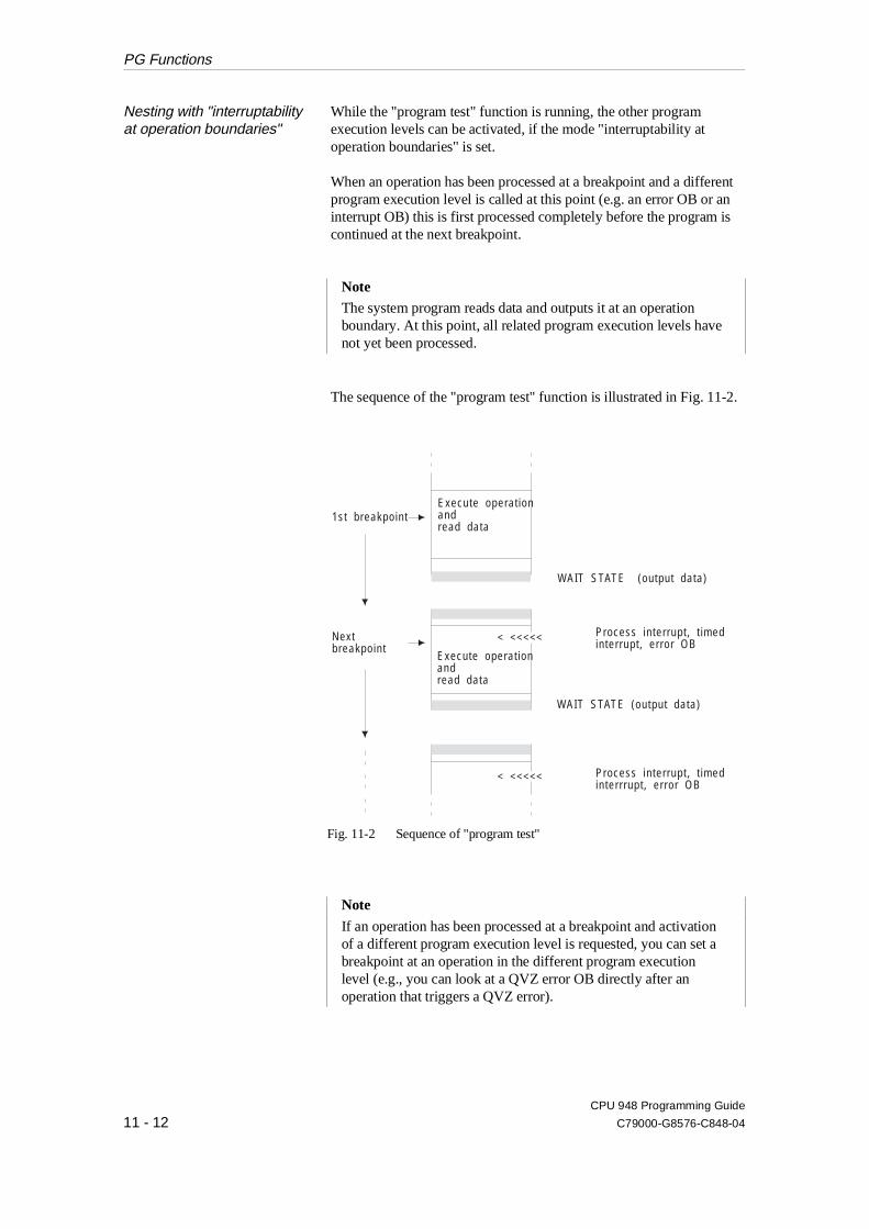
Nesting with "interruptability at operation boundaries"
While the "program test" function is running, the other programexecution levels can be activated, if the mode "interruptability atoperation boundaries" is set.
When an operation has been processed at a breakpoint and a differentprogram execution level is called at this point (e.g. an error OB or aninterrupt OB) this is first processed completely before the program iscontinued at the next breakpoint.
NoteThe system program reads data and outputs it at an operationboundary. At this point, all related program execution levels havenot yet been processed.
The sequence of the "program test" function is illustrated in Fig. 11-2.
Note
If an operation has been processed at a breakpoint and activationof a different program execution level is requested, you can set abreakpoint at an operation in the different program executionlevel (e.g., you can look at a QVZ error OB directly after anoperation that triggers a QVZ error).
Execute operat ionandread data
Execute operat ionandread data
< <<<<<
< <<<<<
1st breakpoint
WAIT STATE (output data)
WAIT STATE (output data)
Process interrupt , t imedinterrrupt, error OB
Process interrupt , t imedinterrupt, error OB
Nextbreakpoint
Fig. 11-2 Sequence of "program test"
PG Functions
CPU 948 Programming Guide
11 - 12 C79000-G8576-C848-04
Interruptions •• Program processing → STOP mode:If an interruption occurs during program processing (e.g., multi-processor stop, I/O not ready/STOP, error OB not programmedetc.) before the program reaches the specified breakpoint, the CPUgoes into the STOP mode immediately. If you execute a COLDRESTART or a MANUAL WARM RESTART, the "program test"function is still in effect and the breakpoint is still set.
•• Program processing at breakpoint → STOP mode:
If stop conditions occur at the breakpoint or following breakpointduring program processing, the CPU goes directly into the softSTOP mode and outputs the data.If you do not specify a new breakpoint while the CPU is in theSTOP mode, the "program test" function is still in effect after therestart.
While the "program test" function is in effect, you can execute thefollowing other functions on your PG
- Output ISTACK
- Output BSTACK
- Load block
- Read block
- Delete block
- Output block list
- Force variables
- Force
In rare situations, the function may be terminated and the CPU issubsequently in the STOP mode.
PG Functions
CPU 948 Programming Guide
C79000-G8576-C848-04 11 - 13
Status variables Using the "status variables" function, you can display the currentsignal states of certain operands (process variables).
When a checkpoint is reached, the PG displays the present signalstatus of the desired process variable. You can display the followingprocess variables: inputs, outputs, flags, timers, counters and datawords. No addressing error (ADF) is triggered in the process imagearea.
Sequence in RUN If the function is active in the RUN mode, the signal states of theoperands are scanned and displayed when the checkpoint is reached.The system program reads inputs from the process image. As long asthe function is not aborted, signal states are updated cyclically.
NoteIf the program does not reach the system checkpoint, the systemprogram does not output the signal states (e.g., in a continuousloop in the user program).
Sequence in SOFT STOP
When the function is active in the STOP mode, the signal states of theoperands are displayed when they exist at the system checkpoint. It isimportant to note that the inputs are scanned and output directly on theI/O module.
Force You can call the "force" PG function to manually set the output bytesof the programmable controller to the signal states you want.
Note
The "force" function is only permitted in the stop mode (SOFTSTOP mode or within the "program test" function).
Sequence of the function When you call the "force" function in the STOP mode, the disableoutput command signal is suppressed (i.e., the BASP LED is off). Alldigital peripherals are cleared (i.e., the value 0 is written to eachaddress). While the peripherals are being cleared, this function cannotbe interrupted. If any timeout signals (QVZs) occur while the outputsare being cleared, they are ignored.
PG Functions
CPU 948 Programming Guide
11 - 14 C79000-G8576-C848-04
The peripheral outputs are forced byte by byte.
In multiprocessor operation, you can force all peripheral outputs(regardless of the peripheral assignment in DB 1).
Timeout errors that occur are detected when outputs are changed (PGmessage "I/O module does not exist").
Terminating the function You can terminate the function by pressing the <BREAK> key on thePG. The disable output command signal is active again (i.e., the"BASP" LED is on). The function also ends if the CPU goes into theRUN mode between calling the function and actually forcing outputs.
Force variables You can call the "force variables" function to look at the values ofoperands (process variables) in the process image table and changethem. You can use this function in the RUN and soft STOP modes andwithin the "program test" function. You can display the followingprocess variables: inputs, outputs, flags, timers, counters and datawords.
Special features Any change becomes effective at the next system checkpoint, i.e.regardless of the system checkpoint (start of cycle or end).
Note that the forced values can be overwritten again (e.g. by the userprogram or by the process image updating).
NoteThe PG forces process variables in bytes.
If you are forcing several operands, the bytes are changed inmemory one after the other distributed over several cycles.
PG Functions
CPU 948 Programming Guide
C79000-G8576-C848-04 11 - 15
11.3 Serial Link PG - PLC via 1st or 2nd Serial Interface
For the serial link PG - PLC there are the following possibilities:
•• Direct link to the CPU via the standard cable.
•• Link to the PG via the coordinator COR C. In this case the PG isconnected via the cable to the coordinator. This means that the 1stserial interface is no longer available.
•• Link to the PG via a PG multiplexer 757. The permitted cables canbe found in the system manual 135U/155U /2/.
•• Link to the PG via SINEC H1/L2/L1 and "swing cable"; theCOR C or PG multiplexer can be connected in the link.
Serial Link PG - PLC via 1st or 2nd Serial Interface
CPU 948 Programming Guide
11 - 16 C79000-G8576-C848-04
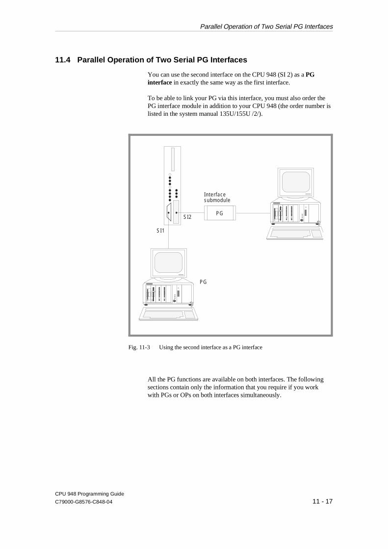
11.4 Parallel Operation of Two Serial PG Interfaces
You can use the second interface on the CPU 948 (SI 2) as a PGinterface in exactly the same way as the first interface.
To be able to link your PG via this interface, you must also order thePG interface module in addition to your CPU 948 (the order number islisted in the system manual 135U/155U /2/).
All the PG functions are available on both interfaces. The followingsections contain only the information that you require if you workwith PGs or OPs on both interfaces simultaneously.
PG
SI1
SI2PG
Inter facesubmodule
Fig. 11-3 Using the second interface as a PG interface
Parallel Operation of Two Serial PG Interfaces
CPU 948 Programming Guide
C79000-G8576-C848-04 11 - 17
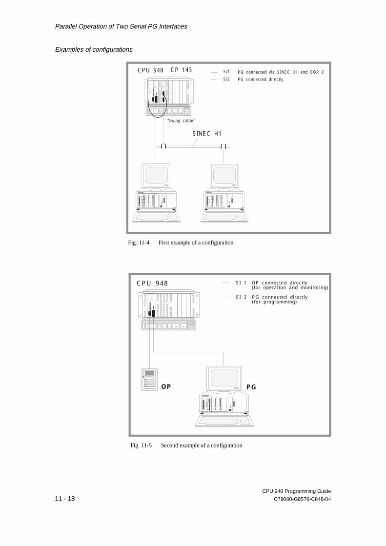
Examples of configurations
CPU 948 CP 143
SINEC H1
SI1 PG connected via SINEC H1 and COR C
SI2
"swing cable"
PG connected direct ly
Fig. 11-4 First example of a configuration
CPU 948
OP PG
SI 2 PG connected direct ly( for programming)
SI 1 OP connected direct ly( for operat ion and monitor ing)
Fig. 11-5 Second example of a configuration
Parallel Operation of Two Serial PG Interfaces
CPU 948 Programming Guide
11 - 18 C79000-G8576-C848-04

11.4.1Installation To use the second interface of the CPU 948 as a PG interface, follow
the steps outlined below:
Step Action
1 Install the PG submodule in the CPU 948.
(refer to the instructions in the Appendix)
2 Connect the PG to the serial interface SI2.
11.4.2Operation If you use the second interface as a PG interface then initially the full
range of functions of the standard PG interface is available on eachinterface. This remains true, providing the individual functions do notinfluence each other, i.e., called sequentially one after the other.
To understand the exceptions to this, the PG functions can be dividedinto three groups:
Group Name
Short-running functions Functions that execute a job and then areterminated. (e.g. "transfer", "delete" etc.)
Long-running functions Functions that process a fixed number ofjobs:
- "force",- "program test".
Cyclic functions Functions that execute a job repeatedlyuntil you terminate them:
- "status block", - "status variables",- "force variables".
Caution
With long-running and cyclic functions you must coordinate theactivation of these functions on both PGs.
Parallel Operation of Two Serial PG Interfaces
CPU 948 Programming Guide
C79000-G8576-C848-04 11 - 19

The table below lists the pairs of functions that you cannot work withsimultaneously.
Function activeon the first PG:
You must not activate this function on the second PG
"Force" Any function
"Program test" Any function
A "status" function" "Force"
A "status" function" "Program test"
A "status" function" "Overall reset"
"Status" on long running blocksor blocks which are not processed
Any function
If you attempt to start one of the illegal functions, the second PGdisplays an error message, e.g.: "AS function disabled: functionactive".
The same error message or "Overflow in data exchange with PG"appears if the CPU 948 is currently processing functions of the otherPG, which prevent your PG accessing the CPU within the monitoringtime. Your input is then rejected. Repeat your input once the functionsare completed on the other PG.
Note
Owing to the different performances and range of functions, timemonitoring and the response to errors is not identical in all PGsand OPs.
If you activate the function "memory configuration"simultaneously on both PGs, the displays may be incorrect.
Caution
If you input, correct or delete blocks online on both PGssimultaneously, you must make sure that the blocks are notprotected by the other PG before you access them."Status" of a block which is not processed or "status" in the STOPmode blocks the other interface for all functions.
Table 11-2 Functions which cannot run simultaneously on both PGs
Parallel Operation of Two Serial PG Interfaces
CPU 948 Programming Guide
11 - 20 C79000-G8576-C848-04
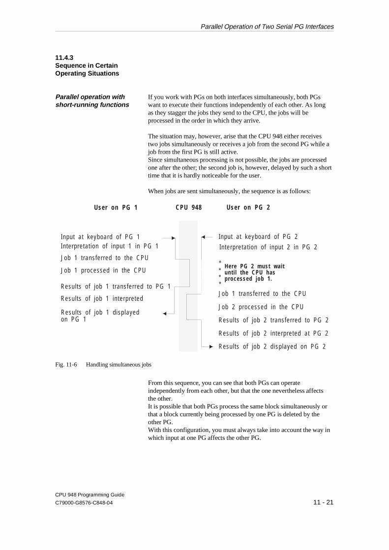
11.4.3Sequence in Certain Operating Situations
Parallel operation withshort-running functions
If you work with PGs on both interfaces simultaneously, both PGswant to execute their functions independently of each other. As longas they stagger the jobs they send to the CPU, the jobs will beprocessed in the order in which they arrive.
The situation may, however, arise that the CPU 948 either receivestwo jobs simultaneously or receives a job from the second PG while ajob from the first PG is still active.Since simultaneous processing is not possible, the jobs are processedone after the other; the second job is, however, delayed by such a shorttime that it is hardly noticeable for the user.
When jobs are sent simultaneously, the sequence is as follows:
From this sequence, you can see that both PGs can operateindependently from each other, but that the one nevertheless affectsthe other. It is possible that both PGs process the same block simultaneously orthat a block currently being processed by one PG is deleted by theother PG.With this configuration, you must always take into account the way inwhich input at one PG affects the other PG.
Input at keyboard of PG 1Interpretat ion of input 1 in PG 1
Job 1 transferred to the CPU
Job 1 processed in the CPU
Resul ts of job 1 transferred to PG 1
Resul ts of job 1 interpreted
Resul ts of job 1 displayedon PG 1
CPU 948User on PG 1
Job 1 transferred to the CPU
Job 2 processed in the CPU
Resul ts of job 2 transferred to PG 2
Resul ts of job 2 interpreted at PG 2
Resul ts of job 2 displayed on PG 2
Input at keyboard of PG 2
Interpretat ion of input 2 in PG 2
****
User on PG 2
Here PG 2 must waitunti l the CPU hasprocessed job 1.
Fig. 11-6 Handling simultaneous jobs
Parallel Operation of Two Serial PG Interfaces
CPU 948 Programming Guide
C79000-G8576-C848-04 11 - 21
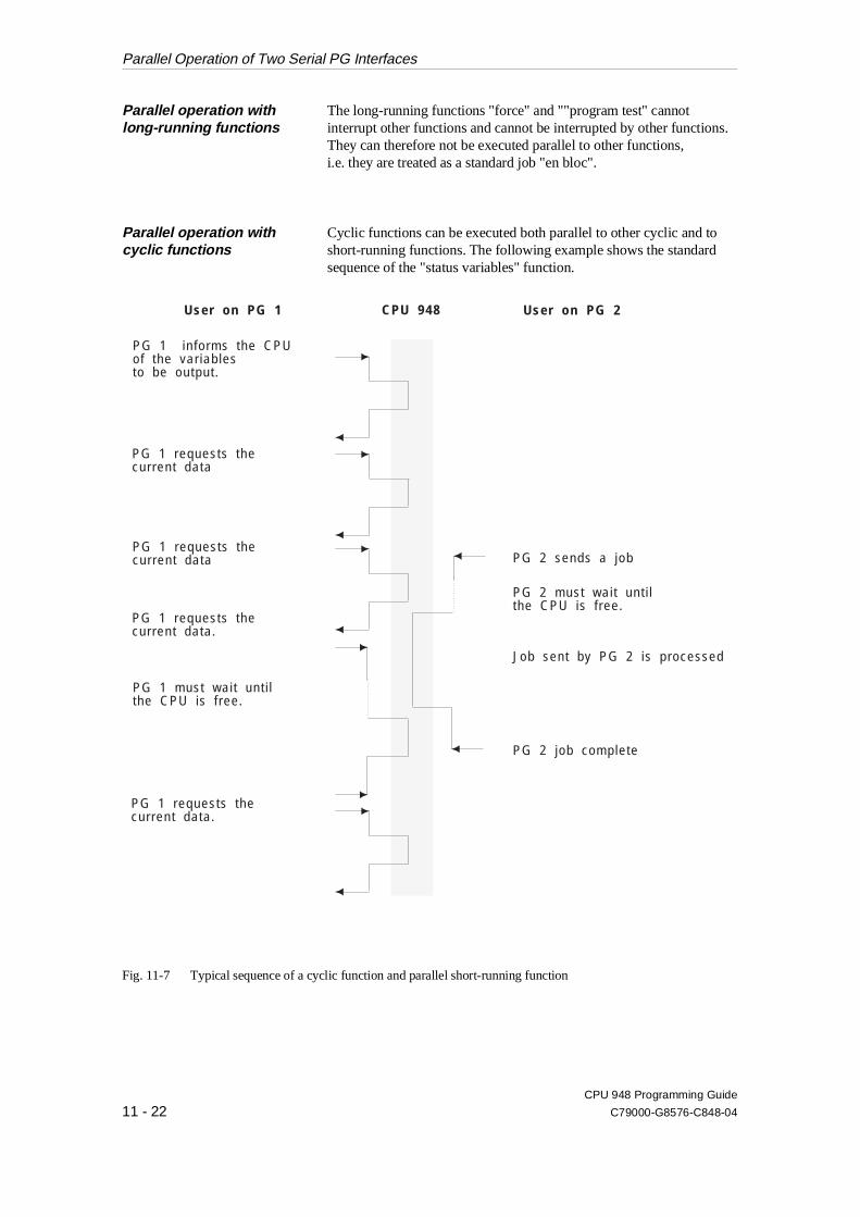
Parallel operation withlong-running functions
The long-running functions "force" and ""program test" cannotinterrupt other functions and cannot be interrupted by other functions.They can therefore not be executed parallel to other functions, i.e. they are treated as a standard job "en bloc".
Parallel operation withcyclic functions
Cyclic functions can be executed both parallel to other cyclic and toshort-running functions. The following example shows the standardsequence of the "status variables" function.
PG 1 informs the CPUof the var iablesto be output.
PG 1 requests thecurrent data
PG 1 requests thecurrent data
PG 1 requests thecurrent data.
PG 1 requests thecurrent data.
PG 1 must wait unt i lthe CPU is free.
Job sent by PG 2 is processed
PG 2 must wait unt i lthe CPU is free.
PG 2 sends a job
PG 2 job complete
CPU 948User on PG 1 User on PG 2
Fig. 11-7 Typical sequence of a cyclic function and parallel short-running function
Parallel Operation of Two Serial PG Interfaces
CPU 948 Programming Guide
11 - 22 C79000-G8576-C848-04
To allow a second PG to send a job to the CPU, the status function isinterrupted between two requests and then continued on completion ofthe inserted job. Since the interrupting function requires CPUfacilities, the whole CPU system facilities must be divided betweenthe two functions, e.g. the updating of the data output by the "statusvariables" function takes somewhat longer.
With both PGs working simultaneously, the sequence shown in figure11.8 results.
This also applies when cyclic functions are active on both PGs; thetwo PGs then access the PLC alternately.
Parallel Operation of Two Serial PG Interfaces
CPU 948 Programming Guide
C79000-G8576-C848-04 11 - 23
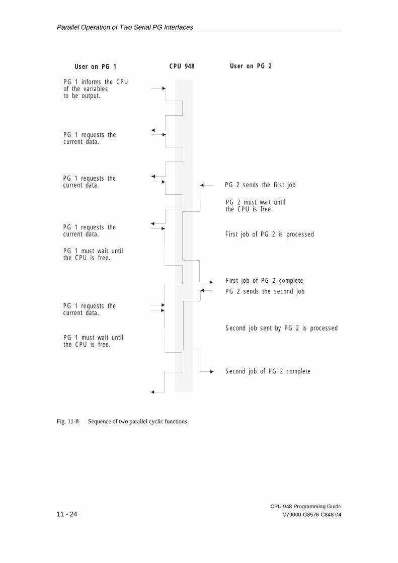
PG 1 informs the CPUof the var iablesto be output.
PG 1 requests thecurrent data.
PG 1 requests thecurrent data.
PG 1 requests thecurrent data.
PG 1 requests thecurrent data.
F irst job of PG 2 is processed
Second job sent by PG 2 is processed
PG 2 sends the f i rst job
PG 2 sends the second job
First job of PG 2 complete
Second job of PG 2 complete
PG 1 must wait unt i lthe CPU is free.
PG 2 must wait unt i lthe CPU is free.
PG 1 must wait unt i lthe CPU is free.
CPU 948User on PG 1 User on PG 2
Fig. 11-8 Sequence of two parallel cyclic functions
Parallel Operation of Two Serial PG Interfaces
CPU 948 Programming Guide
11 - 24 C79000-G8576-C848-04

Special feature with cyclicfunctions on both PGs
If the interrupting function blocks the CPU 948 ("status" in a blockthat is not executed) the interrupted function is also blocked. It canonly be resumed when the interrupting function is terminated.
When working simultaneously with two PGs, the following sequenceresults:
PG 1 informs the CPUof the var iablesto be output.
PG 1 requests thecurrent data.(PG signals: statusprocessing act ive)
PG 1 requests thecurrent data.
PG 1 requests thecurrent data.
PG 1 must wait unt i lthe CPU is free.
PG 2 must wait unt i lthe CPU is free.
Job sent by PG 2 is processed
(PG signals: status processing act ive
(PG signals: statementnot processed)
PG2 sends a new job(e.g. "Status PB 9").
PG 2 job complete
PG 1 receives new data
PG 2 aborts the STATUS funct ion;The CPU processes the abort reques
CPU 948User on PG 1 User on PG 2
Fig. 11-9 Sequence when a function blocks the CPU 948
Parallel Operation of Two Serial PG Interfaces
CPU 948 Programming Guide
C79000-G8576-C848-04 11 - 25

General notes If "status variables", "force variables" (with the status display) or"status" is output on one interface and "compress memory", "deleteblock" or "transfer block" on the other, the status display can becorrupted.
Parallel Operation of Two Serial PG Interfaces
CPU 948 Programming Guide
11 - 26 C79000-G8576-C848-04

11.5 PG Functions via the S5 Bus
11.5.1Application The PG functions via the S5 bus allow you to load and control
S5-155U programmable controllers with the CPU 948 connected viaSINEC H1 using the PG 7xx. With the PG functions via the S5 bus,the CPU 948 can be loaded up to eight times faster than via the PGinterface. The actual speed depends on the length of the blocks to betransferred.
You can also use the PG functions via the S5 bus in the multiprocessormode.
The PG functions via the S5 bus are a component of the systemprogram of the CPU 948.
CautionThe PG functions via the S5 bus can only be used alternatelywith the PG functions via the first and second serial interface (i.e.one function only at a time).With some functions,(simultaneous/nested functions) data or blocks may be corrupted.
With the CPU 948 numbers > 232 are reserved for the PGfunctions via the S5 bus. These numbers are not freely availablefor handling blocks.!
PG Functions via the S5 Bus
CPU 948 Programming Guide
C79000-G8576-C848-04 11 - 27
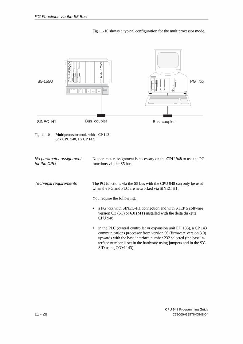
Fig 11-10 shows a typical configuration for the multiprocessor mode.
No parameter assignment for the CPU
No parameter assignment is necessary on the CPU 948 to use the PGfunctions via the S5 bus.
Technical requirements The PG functions via the S5 bus with the CPU 948 can only be usedwhen the PG and PLC are networked via SINEC H1.
You require the following:
•• a PG 7xx with SINEC-H1 connection and with STEP 5 softwareversion 6.3 (ST) or 6.0 (MT) installed with the delta disketteCPU 948
•• in the PLC (central controller or expansion unit EU 185), a CP 143communications processor from version 06 (firmware version 3.0)upwards with the base interface number 232 selected (the base in-terface number is set in the hardware using jumpers and in the SY-SID using COM 143).
Bus couplerBus couplerSINEC H1
CP143
COR923C PG 7xxS5-155U
Fig. 11-10 Multi processor mode with a CP 143(2 x CPU 948, 1 x CP 143)
PG Functions via the S5 Bus
CPU 948 Programming Guide
11 - 28 C79000-G8576-C848-04

11.5.2How the PG Functions Workvia the S5 Bus
Using pages For communication with the CPUs, the CP 143 has four pages(interfaces). If you do not use the PG functions via the S5 bus, all thepages are available for communication using handling blocks (HDBs).
When using the S5 bus functions, the pages of the CPU are dividedinto two pages for user HDBs and two pages for PG functions.The pages for user HDBs can be used as previously for SINEC H1applications. Remember, however, the special features listed inSection 11.5.3.The pages for PG functions are used by the CP 143 and the CPU 948for the PG functions via the S5 bus and are therefore no longeravailable for communication via handling blocks.
Interface numbers (SSNR) The PG functions via the S5 bus are activated automatically in the CP143 when you set the base interface number of the CP to 232 or 236(jumpers and SYSID). You then occupy interface numbers 232 to239. Interface numbers 240 to 247 are intended for later expansions(e.g. CPs with eight pages/interfaces).
SINEC H1
CP 1
CP 2
SINEC H1
SINEC H1
SINEC H1
232
233
234
235
236
237
238
239
.
.
PG functions
PG functions
PG functions
PG functions
reserved (8 pages)
Fig. 11-11 Interface assignment of the PG functions via the S5 bus
PG Functions via the S5 Bus
CPU 948 Programming Guide
C79000-G8576-C848-04 11 - 29

Parameters for the CP 143 Assigning parameters for the CP 143 is described in the CP 143manual (Further Reading /6/).
CautionThe interface numbers 232ff and 236ff must not be assigned onthe CP 143 when operating with other SIMATIC CPUs. Whenoperating the CPU 948 with other CPs, the use of interfacenumbers 232 to 247 is restricted.
Multiprocessor mode The PG functions via the S5 bus can also be used in themultiprocessor mode with the CPU 948.
With one CP 143, two CPUs (948) can use the online functions in theS5-155U. The CP 143 can also be used in the expansion unit (EU 185).In the multiprocessor mode, CPU 1 uses the page with SSNR 234,and CPU 2 the page with SSNR 235.
If a second CP 143 is inserted and has appropriate parametersassigned, this is reserved for the online functions via the S5 bus withCPU 3 and CPU 4 (with SSNR 238 and 239).
PG Functions via the S5 Bus
CPU 948 Programming Guide
11 - 30 C79000-G8576-C848-04
11.5.3Installation and GettingStarted
During installation, remember the following alternatives.
The CP 143 is usedexclusively for PG Functions
If the CP 143 is used exclusively for PG functions via the S5 bus, nofurther parameters other than the SINEC H1 parameters must be set.
After POWER UP, the PG functions are always available on CPU 948via the S5 bus without the CP 143 previously being synchronized withthe HDB SYNCHRON (FB 125). The mode selector on the CPUmust, however, be set to RUN.An "empty" CPU 948 can be started up via the S5 bus without anOVERALL RESET.
After POWER UP, the CPU 948 automatically synchronizes the pagesassigned to it on the CP 143 for PG functions via the S5 bus.
The following steps are necessary for starting up:
Step Action
1 Set the interface number (SSNR) on the CP 143 (jumpers):Select the SSNR according to the existing hardware configuration as shown below.Keep in mind the explanations in Further Reading /6/.
Possible hardware configuration Corresponding SSNR on the CP 143
1 x CPU 948, 1 x CP 143
1 x CPU 948, 2 x CP 143
2 x CPU 948, 1 x CP 143
3 x CPU 948, 2 x CP 143
4 x CPU 948, 2 x CP 143
232
232 on 1st CP, 236 on 2nd CP
232
232 on 1st CP, 236 on 2nd CP
232 on 1st CP, 236 on 2nd CP
2 Insert the CP 143 in the S5-155U (power supply to the PLC must be off).
3 Connect the PG to the PG interface of the CP 143 and load the COM program.
4 Set the interface number selected in step 1 in the SYSID of the CP 143 using COM 143and set the Ethernet address.
PG Functions via the S5 Bus
CPU 948 Programming Guide
C79000-G8576-C848-04 11 - 31
Step Action
5 Load the parameter data on the CP 143:The parameter data of the CP 143 can either be stored- in an EPROM cartridge
or- in the RAM of the CP 143.
You can transfer the parameter data via the serial interface of the PG 7xx. The operations necessary for loading the parameter data of the CP 143 are described in /6/.
6 Perform an overall reset on the CPU, switch the power supply to the PLC off and onagain.
7 Edit the path to the CPU 948 in the bus selection screen form of STEP 5.
8 Select the path to the CPU 948 via SINEC H1/CP 143 in the presets screen form of STEP 5.
Once these actions have been performed, the PG functions can be usedvia the S5 bus. You can now load your user program and run or test it.
Alternative operation via theserial PG interface
At any one time, the CPU 948 only processes one PG function. If youattempt to activate further PG functions on a second PG via the serialPG interface while a PG function is already being processed, amessage, for example, "AS function disabled: function active" isdisplayed on this PG.
Notes If a PG function is aborted by switching the mode selector on the CPUfrom RUN to STOP or by an error, wait times of greater than 15seconds are activated for communication via SINEC H1.
If you make a mistake on the PG (e.g. switching off the PG with a PGfunction still active) it is possible that the "selection" function must berepeated when the path is re-established.
PG Functions via the S5 Bus
CPU 948 Programming Guide
11 - 32 C79000-G8576-C848-04
The CP 143 is used for PGFunctions andCommunication viaSINEC H1
If you use the CP 143 for communication via SINEC H1 as well as forPG functions via the S5 bus, you must make further settings inaddition to those described in Section 3.1 and must take certain specialfeatures into account.
During installation follow the procedure outlined below:
Step Action
1 to 8 Steps 1 to 8 are identical to those described for the alternative "The CP 143 is used exclusivelyfor PG functions"
9 Program the HDB SYNCHRON (FB 125) call in the start-up OBs OB 20 and OB 22 sothat the CP 143 is synchronized for SINEC H1 communication duringMANUAL/AUTOMATIC COLD RESTART and AUTOMATIC WARM RESTART.The HDB SYNCHRON should only be called when the interface is actually used, since theconnection to the PG is subsequently terminated and must then be re-established manually onthe PG.
Using pages forcommunication via handlingblocks
The following diagram illustrates how the PG functions via the S5 bususe the pages of the CP 143. The free pages for user HDBs can beused by CPUs 1 to 4 for communication via SINEC H1.
PG Functions via the S5 Bus
CPU 948 Programming Guide
C79000-G8576-C848-04 11 - 33
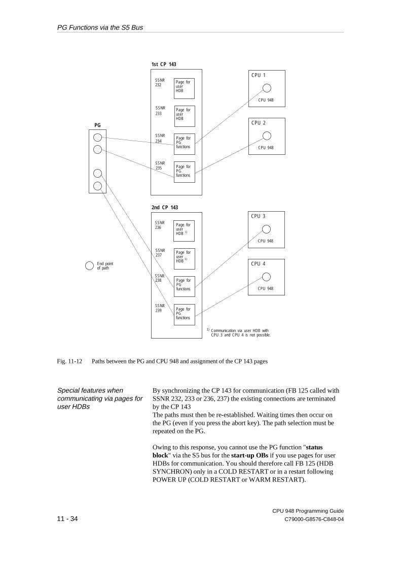
Special features whencommunicating via pages foruser HDBs
By synchronizing the CP 143 for communication (FB 125 called withSSNR 232, 233 or 236, 237) the existing connections are terminatedby the CP 143The paths must then be re-established. Waiting times then occur onthe PG (even if you press the abort key). The path selection must berepeated on the PG.
Owing to this response, you cannot use the PG function "statusblock" via the S5 bus for the start-up OBs if you use pages for userHDBs for communication. You should therefore call FB 125 (HDBSYNCHRON) only in a COLD RESTART or in a restart followingPOWER UP (COLD RESTART or WARM RESTART).
End pointof path
Communication via user HDB withCPU 3 and CPU 4 is not possible.
SSNR
SSNR
SSNR
SSNR
CPU 948
233
237
235
239
234
238
SSNR232
SSNR236
Page foruserHDB
Page foruserHDB
Page foruserHDB
Page foruserHDB
Page forPGfunctions
Page forPGfunctions
Page forPGfunctions
Page forPGfunctions
PG
1)
1)
1)
1st CP 143
2nd CP 143
CPU 1
CPU 948
CPU 2
CPU 948
CPU 3
CPU 948
CPU 4
SSNR
SSNR
Fig. 11-12 Paths between the PG and CPU 948 and assignment of the CP 143 pages
PG Functions via the S5 Bus
CPU 948 Programming Guide
11 - 34 C79000-G8576-C848-04

11.5.4Condition Codes IndicatingProblems
Each of the maximum four CPUs (CPU 948), for which the PGfunctions via the S5 bus are activated, writes condition codes to its RSand RT areas if an error occurs in the PG functions via the S5 bus.
These condition codes consist of a parameter assignment error byte(PAFE) for each possible connection and a condition code word(ANZW) to indicate the current sequence of the transmit and receiveblocks. These codes largely correspond to those of the handling blocks.
RS 50 PAFE codes set during the synchronization of the PG functions arestored in system data word RS 50 (address E F032H).
Evaluating PAFE in RS 50 The PAFE byte is always in the high byte of RS 50.
CPU no. RS 50high byte
RS 50low byte
1 PAFESSNR 234
-
2 PAFESSNR 235
-
3 PAFESSNR 238
-
4 PAFESSNR 239
-
Significance of the PAFEcodes
All errors are indicated which occur in the interaction with theCP 143. The following PAFE codes are then set:
PAFE value Significance
00H No error
71H Interface (page) does not exist
81H Interface not ready
91H Interface overloaded
A1H Interface being used by a different CPU
B1H Job number or field size illegal (FB SYNCHRON)
C1H Interface not responding or not in time
D1H Other interface errors, also error code for the CP
PG Functions via the S5 Bus
CPU 948 Programming Guide
C79000-G8576-C848-04 11 - 35

Meaning of the code 71H:
The code 71H means that the page does not exist. If this error occurs,the PG functions cannot be used via the S5 bus. In this case, check theinterface assignment of the CP 143. Interface numbers 232ff or 236ffmust be set (jumpers and SYSID!).
RT area If the pages for PG functions exist and the connection to the CP 143 isestablished, an information field consisting of 16 words is set up in theRT area of the CPU 948 with the structure shown below.
NoteAs long as there is no connection to the CP 143 (PAFE = 71), e.g.because there is no page with SSNR 232ff or 236ff, no additionalinformation is stored in the RT area.
Address
E F2E8H Data sent from CPU to PG forinterface 234 or 238
RT 232
E F2E9H Data sent from CPU to PG forinterface 235 or 239
RT 233
E F2EAH reserved RT 234
E F2EBH reserved RT 235
E F2ECH Data sent from PG to CPU forinterface 234 or 238
RT 236
E F2EDH Data sent from PG to CPU forinterface 235 or 239
RT 237
E F2EEH reserved RT 238
E F2EFH reserved RT 239
E F2F0H reserved PAFE 234 RT 240
E F2F1H reserved reserved RT 241
E F2F2H reserved PAFE 235 RT 242
E F2F3H reserved reserved RT 243
E F2F4H reserved PAFE 238 RT 244
E F2F5H reserved reserved RT 245
E F2F6H reserved PAFE 239 RT 246
E F2F7H reserved reserved RT 247
PG Functions via the S5 Bus
CPU 948 Programming Guide
11 - 36 C79000-G8576-C848-04
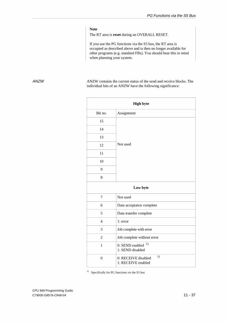
NoteThe RT area is reset during an OVERALL RESET.
If you use the PG functions via the S5 bus, the RT area isoccupied as described above and is then no longer available forother programs (e.g. standard FBs). You should bear this in mindwhen planning your system.
ANZW ANZW contains the current status of the send and receive blocks. Theindividual bits of an ANZW have the following significance:
High byte
Bit no. Assignment
15
Not used
14
13
12
11
10
9
8
Low byte
7 Not used
6 Data acceptance complete
5 Data transfer complete
4 1: error
3 Job complete with error
2 Job complete without error
1 0: SEND enabled 1)
1: SEND disabled
0 0: RECEIVE disabled 1)
1: RECEIVE enabled
1) Specifically for PG functions via the S5 bus
PG Functions via the S5 Bus
CPU 948 Programming Guide
C79000-G8576-C848-04 11 - 37

PG Functions via the S5 Bus
CPU 948 Programming Guide
11 - 38 C79000-G8576-C848-04
Contents of Chapter 12
Appendix 1: Jumper Settings for System Interrupts . . . . . . . . . . . . . . . . . . . . . . . . . . . . . . . . . . . . . . . 12 - 4
Appendix 2: Inserting and Removing the PG Submodule. . . . . . . . . . . . . . . . . . . . . . . . . . . . . . . . . . . 12 - 5
Appendix 3: Technical Data of the CPU 948 and CPU 928B . . . . . . . . . . . . . . . . . . . . . . . . . . . . . . . . 12 - 7
Appendix 4: Results IDs of some of the Special Function OBs in ACCU 1 . . . . . . . . . . . . . . . . . . . 12 - 10
12Appendix
CPU 948 Programming Guide
C79000-G8576-C848-04 12 - 1

Contents
CPU 948 Programming Guide
12 - 2 C79000-G8576-C848-04
12Appendix
This chapter provides additional information about the CPU 948 suchas jumper settings for system interrupts, notes on inserting andremoving the PG submodule, comparisons of runtimes withCPU 946/947 and CPU 928B, and results IDs of some of the specialfunction OBs .
CPU 948 Programming Guide
C79000-G8576-C848-04 12 - 3
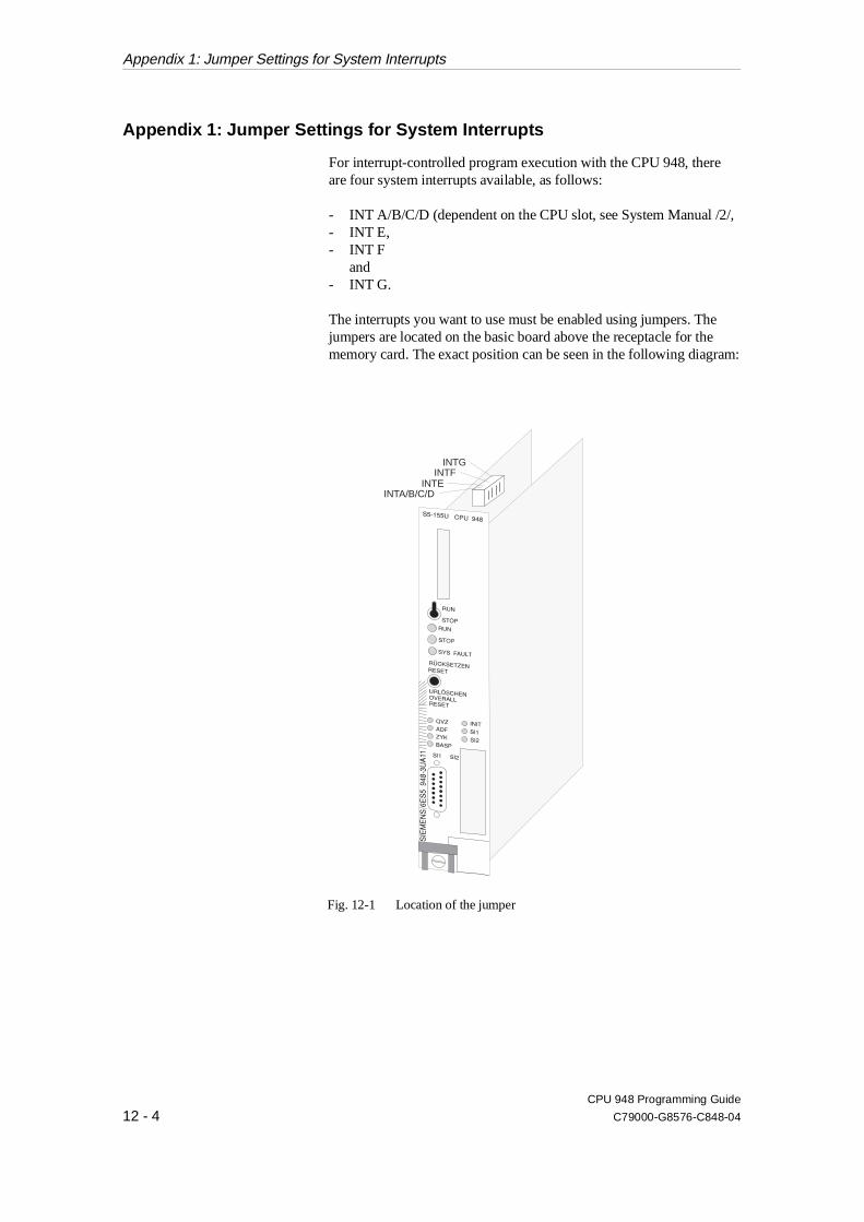
Appendix 1: Jumper Settings for System Interrupts
For interrupt-controlled program execution with the CPU 948, thereare four system interrupts available, as follows:
- INT A/B/C/D (dependent on the CPU slot, see System Manual /2/,- INT E,- INT F
and- INT G.
The interrupts you want to use must be enabled using jumpers. Thejumpers are located on the basic board above the receptacle for thememory card. The exact position can be seen in the following diagram:
INTFINTG
INTEINTA/B/C/D
Fig. 12-1 Location of the jumper
Appendix 1: Jumper Settings for System Interrupts
CPU 948 Programming Guide
12 - 4 C79000-G8576-C848-04
Appendix 2: Inserting and Removing the PG Submodule
If you want to use a PG submodule, this must first be added to theCPU (before the CPU is installed in the central controller).
CautionSwitch off the power supply to the programmable controllerbefore you remove the CPU.
Inserting the submoduleNoteThe jumpers on the PG submodule are already correctly set whensupplied. If, following installation you encounter difficulties,compare the jumper setting with the settings shown in the SystemManual /2/.
Insert your PG submodule as follows:
Step Action
1 Switch off the power supply to your PLC.
2 Remove the CPU from the central controller.
3 Undo the two screws securing the cover of the submodulereceptacle on the CPU and remove the cover.
4 Insert the PG submodule through the front panel into theconnector (components in the same direction as those ofthe CPU).
5 Secure the submodule with the two screws previouslyused for the cover.
6 Insert the CPU in the central controller.
7 Switch on the power supply to your PLC again.
Appendix 2: Inserting and Removing the PG Submodule
CPU 948 Programming Guide
C79000-G8576-C848-04 12 - 5

Removing the submodule You remove the PG submodule as follows:
Step Action
1 Switch off the power supply to your PLC.
2 Remove the CPU from the central controller.
3 Undo the two screws securing the submodule and removethe submodule from the receptacle.
4 Insert a further submodule (as described above) or closethe submodule receptacle with the cover. Use the samescrews used to secure the submodule.
6 Insert the CPU in the central controller.
7 Switch the power supply to your PLC on again.
NoteScrewing the interface submodule to the CPU diverts disturbancepulses via the screen of the CPU. The CPU must only be operatedwith the submodule receptacle closed (cover or submodule).
Appendix 2: Inserting and Removing the PG Submodule
CPU 948 Programming Guide
12 - 6 C79000-G8576-C848-04

Appendix 3: Technical Data of the CPU 948 and CPU 928B
Operation / Processing CPU 948 CPU 928B
Typical command execution times for bit commands:
withF, I, Q
DFormal operand
0.18 µs 0.7 µs 0.91 µs
0.57 µs 3.4 µs 2.4 µs
Typical command execution times for word commands:
- Load operations L FY (byte) L FW (word) L FD (double word)
0.18 µs0.5 µs0.71 µs
0.81 µs0.9 µs1.6 µs
- Fixed point arithmetic- Floating point arithmetic
0.55 ... 3.8 µs 3.3 ... 6.3 µs
0.9 ... 10.4 µs 9.1 ... 15.6 µs
Cyclic program execution (single processor mode)
Basic overhead calling OB 1/FB 0: 65/– µs 104/106 µs
Extra time for process image updating depending onthe number of I/O bytes (n)
where 0 < n ≤128
n ≤ 64: 64 µs + n * 2.3 µs
n > 64: 92 µs + n * 2.3 µs
I: 14 µs + n * 1.1 µs
Q: 5 µs + n * 4.1 µs
Extra time for IPC flag transfer depending on thenumber of IPC flags (n)
where 0 < n ≤ 256
n ≤ 64: 64 µs + n * 2.1 µs
n > 64: 92 µs + n * 2.1 µs
I: 14 µs + n * 1.4 µs
Q: 5 µs + n * 4.3 µs
Extra time for timer processing depending on thetimer block length
Timer block length (TBL) = 0 every 10 ms
11.6 µs every 10 ms
10 µs
timer block length #0n = number of timers running(steps: 10 ms)
11.6 µs + TBL* 0.32 µs 16 µs + TBL * 0.2 µs(no difference between running and stopped
timers)
Interrupt driven program execution
Cycle time extension from nesting an empty OB 2(without STEP 5 operations) at a block boundary 262 µs 300 µs
Reaction time 175 µs 270 µs
Appendix 3: Technical Data of the CPU 948 and CPU 928B
CPU 948 Programming Guide
C79000-G8576-C848-04 12 - 7

Operation / Processing CPU 948 CPU 928B
Time-driven program execution
Cycle time extension from nesting an empty OB 13(without STEP 5 operations) at a block boundary 287 µs
310 µs for the 1st timedint. OB
170 µs for each furthertimed int. OB due at the
same time
Clock rate for time-driven program (timed interrupts OB 10 to OB 18)
Variablebasic clock rate
from 1 to 255 ms.Spec. in steps of
10 ms:10, 20, 50, 100200, 500 ms,
1, 2, 5 sor
10, 20, 40, 80, 160,320, 640 ms,1.28, 2.56 s
10, 20, 50, 100, 200, 500 ms,
1, 2, 5 sec
Resolution for clock-driven timed interrupts(OB 9)
every minute,hourly,daily,
weekly,monthly,yearly,once
every minute,hourly,daily,
weekly,monthly,yearly,once
Resolution for delayed interrupt (OB 6) 1 ms 1 ms
Cycle time monitoring
Defaultselectable betweentriggerable
200 ms1 to 2550 ms
yes
150 ms1 to 13000 ms
yes
Memory sizes
Size of the user memory module(in Kbytes) 640 or
166464
Size of memory for data blocks (DB-RAM, inKbytes)
– approx. 46.6
Timers, counters and flags
Number of timers and counters 256 of each 256 of each
Number of flags 2048 flags+ 32768 S flags
2048 flags+ 8192 S flags
Appendix 3: Technical Data of the CPU 948 and CPU 928B
CPU 948 Programming Guide
12 - 8 C79000-G8576-C848-04
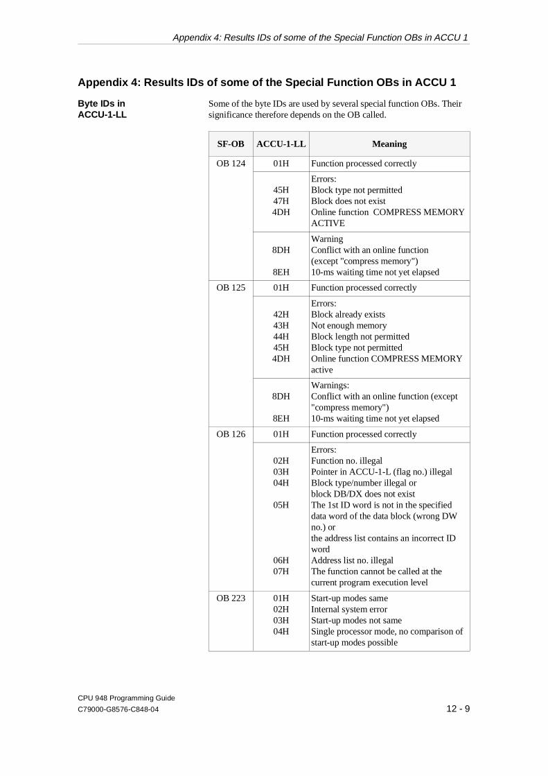
Appendix 4: Results IDs of some of the Special Function OBs in ACCU 1
Byte IDs in ACCU-1-LL
Some of the byte IDs are used by several special function OBs. Theirsignificance therefore depends on the OB called.
SF-OB ACCU-1-LL Meaning
OB 124 01H Function processed correctly
45H47H4DH
Errors:Block type not permittedBlock does not existOnline function COMPRESS MEMORYACTIVE
8DH
8EH
WarningConflict with an online function(except "compress memory")10-ms waiting time not yet elapsed
OB 125 01H Function processed correctly
42H43H44H45H4DH
Errors:Block already existsNot enough memoryBlock length not permittedBlock type not permittedOnline function COMPRESS MEMORYactive
8DH
8EH
Warnings:Conflict with an online function (except"compress memory")10-ms waiting time not yet elapsed
OB 126 01H Function processed correctly
02H03H04H
05H
06H07H
Errors:Function no. illegalPointer in ACCU-1-L (flag no.) illegalBlock type/number illegal orblock DB/DX does not existThe 1st ID word is not in the specifieddata word of the data block (wrong DWno.) orthe address list contains an incorrect IDwordAddress list no. illegalThe function cannot be called at thecurrent program execution level
OB 223 01H02H03H04H
Start-up modes sameInternal system errorStart-up modes not sameSingle processor mode, no comparison ofstart-up modes possible
Appendix 4: Results IDs of some of the Special Function OBs in ACCU 1
CPU 948 Programming Guide
C79000-G8576-C848-04 12 - 9

SF-OB ACCU-1-LL Meaning
OB 254/255
01H Function processed correctly
41H
43H48H4AH
4BH
4CH
4DH
4EH
Errors:Block header on memory cardinvalidNot enough memorySource data block does not existBlock number or type illegal/source DBBlock number or typeillegal/destination DBDestination data block already exists inuser memoryOnline function COMPRESS MEMORYactiveNo memory card inserted
8DH
8EH
Warnings:Conflict with an online function(except COMPRESS MEMORY)10-ms waiting time not yet elapsed
Appendix 4: Results IDs of some of the Special Function OBs in ACCU 1
CPU 948 Programming Guide
12 - 10 C79000-G8576-C848-04
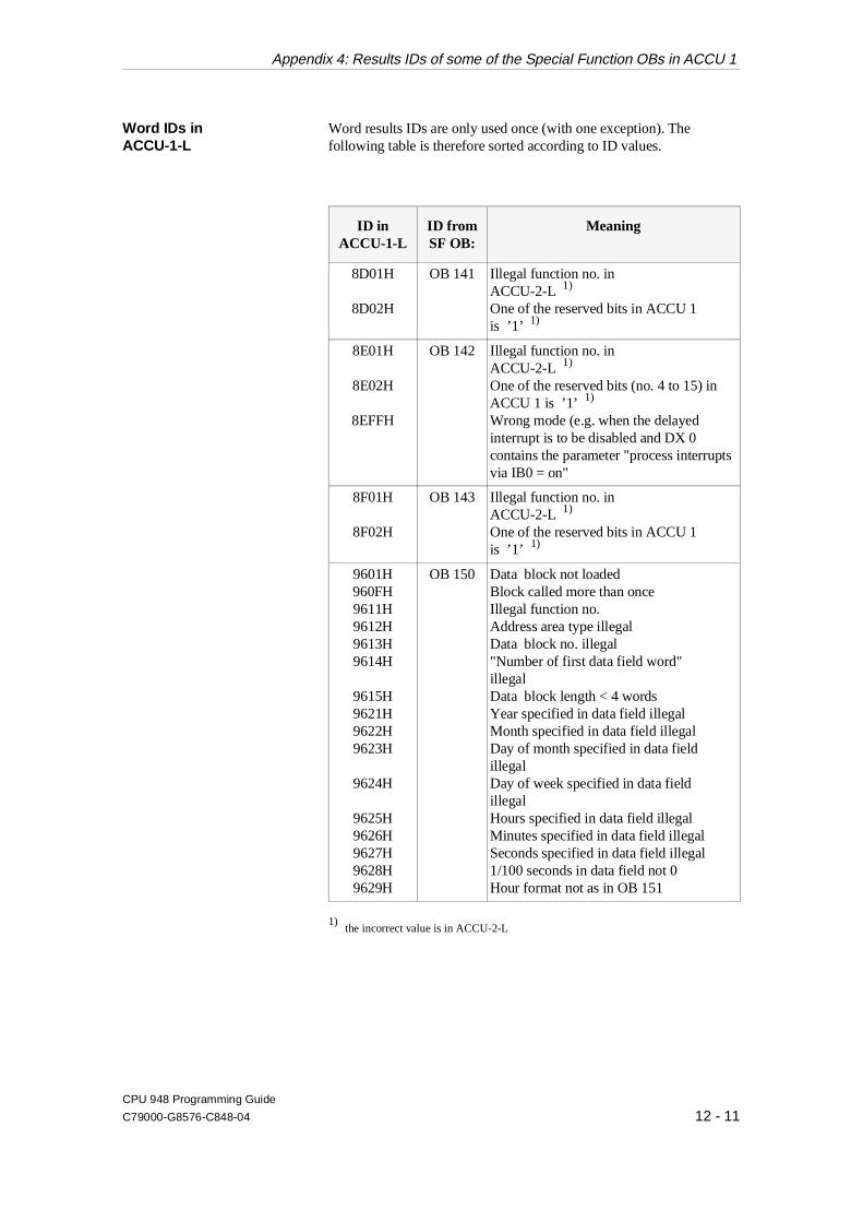
Word IDs in ACCU-1-L
Word results IDs are only used once (with one exception). Thefollowing table is therefore sorted according to ID values.
ID inACCU-1-L
ID fromSF OB:
Meaning
8D01H
8D02H
OB 141 Illegal function no. in ACCU-2-L 1)
One of the reserved bits in ACCU 1 is ’1’ 1)
8E01H
8E02H
8EFFH
OB 142 Illegal function no. in ACCU-2-L 1)
One of the reserved bits (no. 4 to 15) inACCU 1 is ’1’ 1)
Wrong mode (e.g. when the delayedinterrupt is to be disabled and DX 0contains the parameter "process interruptsvia IB0 = on"
8F01H
8F02H
OB 143 Illegal function no. in ACCU-2-L 1)
One of the reserved bits in ACCU 1 is ’1’ 1)
9601H960FH9611H9612H9613H9614H
9615H9621H9622H9623H
9624H
9625H9626H9627H9628H9629H
OB 150 Data block not loadedBlock called more than onceIllegal function no.Address area type illegalData block no. illegal"Number of first data field word"illegalData block length < 4 wordsYear specified in data field illegalMonth specified in data field illegalDay of month specified in data fieldillegalDay of week specified in data fieldillegalHours specified in data field illegalMinutes specified in data field illegalSeconds specified in data field illegal1/100 seconds in data field not 0Hour format not as in OB 151
1) the incorrect value is in ACCU-2-L
Appendix 4: Results IDs of some of the Special Function OBs in ACCU 1
CPU 948 Programming Guide
C79000-G8576-C848-04 12 - 11
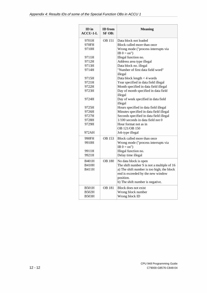
ID inACCU-1-L
ID fromSF OB:
Meaning
9701H970FH9710H
9711H9712H9713H9714H
9715H9721H9722H9723H
9724H
9725H9726H9727H9728H9729H
972AH
OB 151 Data block not loadedBlock called more than onceWrong mode ("process interrupts viaIB 0 = on")Illegal function no.Address area type illegalData block no. illegal"Number of first data field word"illegalData block length < 4 wordsYear specified in data field illegalMonth specified in data field illegalDay of month specified in data fieldillegalDay of week specified in data fieldillegalHours specified in data field illegalMinutes specified in data field illegalSeconds specified in data field illegal1/100 seconds in data field not 0Hour format not as in OB 121/OB 150Job type illegal
990FH9910H
9911H9921H
OB 153 Block called more than onceWrong mode ("process interrupts viaIB 0 = on")Illegal function no.Delay time illegal
B401HB410HB411H
OB 180 No data block is openThe shift number S is not a multiple of 16a) The shift number is too high; the blockend is exceeded by the new windowposition.b) The shift number is negative.
B501HB502HB503H
OB 181 Block does not existWrong block numberWrong block ID
Appendix 4: Results IDs of some of the Special Function OBs in ACCU 1
CPU 948 Programming Guide
12 - 12 C79000-G8576-C848-04
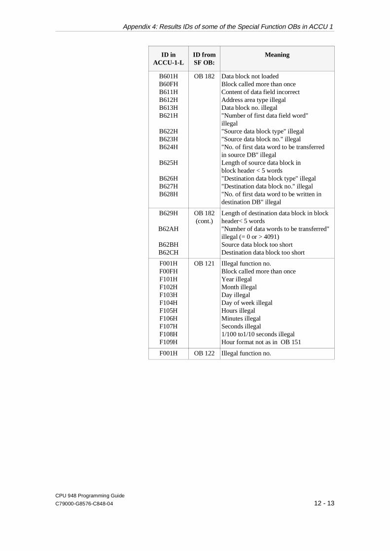
ID inACCU-1-L
ID fromSF OB:
Meaning
B601HB60FHB611HB612HB613HB621H
B622HB623HB624H
B625H
B626HB627HB628H
OB 182 Data block not loadedBlock called more than onceContent of data field incorrectAddress area type illegalData block no. illegal"Number of first data field word"illegal"Source data block type" illegal"Source data block no." illegal"No. of first data word to be transferredin source DB" illegalLength of source data block inblock header < 5 words"Destination data block type" illegal"Destination data block no." illegal"No. of first data word to be written indestination DB" illegal
B629H
B62AH
B62BHB62CH
OB 182(cont.)
Length of destination data block in blockheader< 5 words"Number of data words to be transferred"illegal (= 0 or > 4091)Source data block too shortDestination data block too short
F001HF00FHF101HF102HF103HF104HF105HF106HF107HF108HF109H
OB 121 Illegal function no.Block called more than onceYear illegalMonth illegalDay illegalDay of week illegalHours illegalMinutes illegalSeconds illegal1/100 to1/10 seconds illegalHour format not as in OB 151
F001H OB 122 Illegal function no.
Appendix 4: Results IDs of some of the Special Function OBs in ACCU 1
CPU 948 Programming Guide
C79000-G8576-C848-04 12 - 13

Appendix 4: Results IDs of some of the Special Function OBs in ACCU 1
CPU 948 Programming Guide
12 - 14 C79000-G8576-C848-04

Contents of Chapter 13
List of Abbreviations . . . . . . . . . . . . . . . . . . . . . . . . . . . . . . . . . . . . . . . . . . . . . . . . . . . . . A - 1
List of Key Words. . . . . . . . . . . . . . . . . . . . . . . . . . . . . . . . . . . . . . . . . . . . . . . . . . . . Index - 1
13Indexes
CPU 948 Programming Guide
C79000-G8576-C848-04 13 - 1

Contents
CPU 948 Programming Guide
13 - 2 C79000-G8576-C848-04

Abbreviations
(An explanation of the ISTACK abbreviations can be found in Section 5.4)
ACCU-1 (2, 3, 4)-L low word in accumulator 1 (2, 3, 4), 16 bitACCU-1 (2, 3, 4)-H high word in accumulator 1 (2, 3, 4), 16 bitACCU-1 (2 ,3, 4)-LL low byte of low word in accumulator 1 (2, 3, 4), 8 bitACCU-1 (2, 3, 4)-LH high byte of low word in accumulator 1 (2, 3, 4), 8 bitADF addressing errorANZW condition code word
BASP disable command output (signal on S5 bus)BCD binary coded decimalBR base address registerBSTACK block stack
CC 1, CC 0 condition code bits for digital operationsCOR coordinator moduleCP communications processorCPU central processing unit CSF control system flowchart
DB data blockDBA data block start address (in register 6)DBL data block length (in register 8)DX extended data block
EPROM erasable programmable read only memoryERAB first scan (bit code)EU expansion unit
FB function blockFX extended function block
IM interface moduleINT (system)interruptIP intelligent peripheral moduleISTACK interrupt stack
List of Abbreviations
List of Abbreviations
CPU 948 Programming Guide
C79000-G8576-C848-04 A - 1
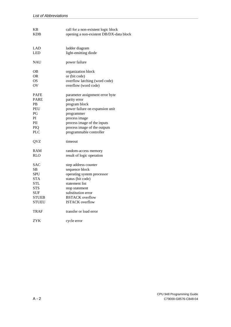
KB call for a non-existent logic blockKDB opening a non-existent DB/DX-data block
LAD ladder diagramLED light-emitting diode
NAU power failure
OB organization blockOR or (bit code)OS overflow latching (word code)OV overflow (word code)
PAFE parameter assignment error bytePARE parity errorPB program blockPEU power failure on expansion unit PG programmer PI process imagePII process image of the inputsPIQ process image of the outputsPLC programmable controller
QVZ timeout
RAM random-access memoryRLO result of logic operation
SAC step address counterSB sequence blockSPU operating system processorSTA status (bit code)STL statement listSTS stop statementSUF substitution errorSTUEB BSTACK overflowSTUEU ISTACK overflow
TRAF transfer or load error
ZYK cycle error
List of Abbreviations
CPU 948 Programming Guide
A - 2 C79000-G8576-C848-04
List of Key Words
A
access to DW 255 9-15ACCU writing conventions 6-5accumulators 6-26actual operands
of function blocks 2-29ADF (addressing error) 5-26arithmetic operations 3-57assignment list 2-24
B
basic operations 2-4, 3-19BASP signal 4-26, 4-29binary logic operations 3-50binary numbers 2-8block
block preheader 2-35body 2-13, 2-24, 2-36formal operands (block parameters) 2-27header 2-13, 2-36number 2-12, 2-36, 3-33preheader 2-14
block address list 3-8, 8-13block calls 2-16, 3-8, 3-32block ID 2-36block operations 3-32blocks
deleting 6-14generating 6-17
BR register 9-22BSTACK (block stack) 5-5
evaluating 5-7output 5-6
C
CC 1 and CC 0see results codes
checkpoints 11-5clock-controlled interrupt 4-33, 4-35, 6-43clock-controlled interrupts 4-29
COLD RESTART 4-21collision of timed interrupts 4-39communication OBs 10-22
condition code byte 10-25parameters 10-23runtimes 10-31
communication processors (CPs) 10-7comparison operations 3-32control bits 5-5, 5-9correcting blocks 2-15counter value 3-28counters C 1-13CPU type and ID 8-44CSF (control system flowchart) 2-4CYCLE 3-11, 4-30
interrupt points 4-31program execution level 4-29user interface OB 1 4-31
cycle monitoring time 6-63cycle time
used 8-41cyclic communication 4-9cyclic processing 1-5cyclic program execution 1-16, 4-30cyclic timed interrupt 4-33cyclic timed interrupts 4-29, 4-37
D
data area 6-59data block DB 0 2-41, 3-8, 8-13data block DB 1 2-41data block DB 2 2-41data block DX 0 2-41, 7-4
parameters 7-8structure 7-5
data block DX 1 2-41data blocks
general 1-13data blocks (DB/DX)
copying from memory card 6-65copying/duplicating 6-65general 2-13, 2-35generating 3-33programming 2-37structure 2-35
List of Key Words
CPU 948 Programming GuideC79000-G8576-C848-04 Index - 1
testing 6-57validity 2-38
data word 1-13, 2-35, 2-39date 6-38DBA (data block start address) 9-11DBL (data block length) 9-13decimal numbers 2-8decrementing 3-66defaults, modifying 1-8delay interrupts 6-32, 6-35delayed interrupt 4-29, 4-33 - 4-34, 6-50digital logic operations 3-50disable interrupts 6-12, 6-29dual-port RAM 9-29
E
ERABsee results codes
error analysis 5-8error in self-test 5-33error information 5-5errors
avoiding 5-4cause 5-23handling 5-20
F
F flags 1-12, 10-23FEDBX (error in G DB/GX DX) 5-32fixed point numbers 2-9flags
multiple use 4-46floating point numbers 2-8formal operands 2-25, 3-52function blocks (FB/FX)
general 2-13, 2-23programming 2-25standard function blocks 2-23, 2-33structure 2-24
G
global memoryaccess 9-25general 9-4
GRAPH 5 2-5
H
hot restart 4-27
I
I/Osmodules 1-11O area 1-11P area 1-11
incrementing 3-66interface to system program 1-8, 1-10, 2-18interprocessor communication flags
data exchange via IPCs 10-5general 3-13, 10-5jumper settings 10-5
interrupt-driven processing 1-6interrupt-driven program execution 4-32, 4-41interrupts
jumper settings 12-4interrupts
general 4-43ISTACK 4-5ISTACK (interrupt stack)
code bits 5-15contents 5-14error information 5-5information in ISTACK 5-15output 5-6, 5-9
J
jump operations 3-59
L
LAD (ladder diagram) 2-4LED display 4-12 - 4-13library number 2-36load operations 3-21, 3-55local memory
access 9-24general 9-4
logic operations 3-50
List of Key Words
CPU 948 Programming GuideIndex - 2 C79000-G8576-C848-04
M
mantissasee floating point number
memory access 9-6via the BR register 9-22via address in ACCU 1 9-8
memory card 3-10memory organization 9-4mode of operation of CPU 1-5multiprocessor communication 6-62
application examples 10-53assignment list 10-37buffering data 10-17data amount 10-15initializing 10-33modes 10-35receive data 10-47send data 10-40sequence 10-15test mode 10-14
multiprocessor modedata exchange between CPUs and CPs 10-7data exchange with HDBs 10-8programming 10-9
N
NAU (power failure) 4-19, 4-28nesting depth 3-9nesting program execution levels 4-6no operation 3-33
O
O area see I/Osoperand areas 1-11OR see results codesorganization block (OB)
general 2-12, 2-16organization blocks
for communication in SOFT STOP 2-20organization blocks (OB)
as user interfaces 2-18for processing errors 2-20special function organization blocks 6-4
OS (overflow latching)see results codes
OV (overflow) see results codesOVERALL RESET 4-14
P
P areasee I/Os
page area/DPRoccupied register 9-30
pagesaccessing 9-29
parameters for DX 0 1-8PARE (parity error) 5-28PG functions 11-4PG functions via S5 bus 11-27PG interface module 11-17PG screen form
for DX 0 parameter assignment 7-14for generating DB1 10-10
PG software 1-18PG submodule
installing 12-5removing 12-6
PLC identification field 8-42priority 1-6, 4-5, 4-7, 4-33, 4-42, 7-10process image
outputs (PIQ) 1-5defining/transferring 6-20inputs (PII) 1-5general 1-11inputs (PII) 1-11outputs (PIQ) 1-11updating 4-29
PROCESS INTERRUPT 4-29process interrupts
disable 3-72enable 3-72, 4-45
process interrupts via input byte IB 0general 4-41user interfaces 4-41
programstoring 3-10program blocks (PB) 2-12, 2-16program execution level
general 4-6, 6-32program execution levels 4-4programming
general 1-15programming language
C with S5-C compiler 1-18GRAPH 5 1-18SCL 1-18STEP 5 1-18
programming language SCL 1-18programming tools 1-18
List of Key Words
CPU 948 Programming GuideC79000-G8576-C848-04 Index - 3

Q
QVZ (timeout error) 5-25
R
reaction time 4-46reactions with error OBs not loaded 5-21real-time clock 8-32results codes
ERAB 3-16, 3-20CC 1 and CC 0 3-18, 3-61OR 3-17OS 3-17OV 3-17RLO 2-7, 3-17, 3-20STA 3-17, 3-20
RI/RJ area 8-14RLO
see results codesRS/RT area 8-15
assignment of RS area 8-16RUN
general 4-29
S
S flags 1-12S-6 (communication error) 5-32scratchpad flags 10-53self-test 5-34
activating/deactivating tests 5-37control bits 8-40error handling 5-38error information 5-39
sequence blocks (SB) 2-12serial link PG - PLC 11-16set/reset operation 3-20shift operations 3-61software protection 8-35special functions
calling 6-5errors in processing 6-6general 6-4interfaces to special functions 6-5
STA (status)see results codes
standard function blockssee also function blocks
START-UP 3-11general 3-11, 4-16
interruptions 4-28triggering 4-17, 4-19
start-up typescomparing 6-64
starting up 10-13STEP 5 operations 3-15STL (statement list) 2-4STOP
mode 4-9stop operations 3-33structure of the memory area 8-4 - 8-5structured programming 2-5sub-level 4-7SUF (substitution error) 5-28suitability of the CPU 948 1-4supplementary operations 2-4system data 8-15system data words
bit assignment 8-18system interrupt
see interrupt 12-4system interrupts 7-9system operations 2-4, 3-59, 9-4system program 1-7system program defaults 1-8system RAM 8-6system time 6-8, 6-38
T
testing address lines 5-36testing the block code 5-36testing the hardware clock 5-35testing the system program code 5-36testing the user memory 5-35time slice 5-34
calculating 5-37setting the number 5-37
time-controlled processing 1-6time-controlled program execution 4-33timed interrupts 4-29, 7-8timed job 4-35, 6-43timer and counter operations 3-26, 3-53timers T 1-13TRAF (load and transfer error) 5-29transfer operations 3-21, 3-55transferring memory fields 9-19
U
user interfacesfor clock-controlled interrupt 4-35
List of Key Words
CPU 948 Programming GuideIndex - 4 C79000-G8576-C848-04

for cyclic program execution 4-31for delayed interrupt 4-34for interrupts 4-44for process interrupts 4-41for start-up 4-24for timed interrupts 4-38
user memory 1-14, 3-10user program 1-7, 1-9
processing 3-4, 3-11see programstoring 1-10tasks 1-9
W
WARM RESTART 4-21WEFES/WEFEH (collision of timed interrupts) 5-30
Z
ZYK (cycle time error) 5-27
List of Key Words
CPU 948 Programming GuideC79000-G8576-C848-04 Index - 5

List of Key Words
CPU 948 Programming GuideIndex - 6 C79000-G8576-C848-04

CPU 948 Programming GuideC79000-G8576-C848-04 1�
Siemens AG
A&D AS E 81
Östliche Rheinbrückenstr. 50
D-76181 Karlsruhe
Federal Republic of Germany
Please check any industry that applies to you:
� Automotive
� Chemical
� Electrical Machinery
� Food
� Instrument and Control
� Nonelectrical Machinery
� Petrochemical
� Pharmaceutical
� Plastic
� Pulp and Paper
� Textiles
� Transportation
� Other _ _ _ _ _ _ _ _ _ _ _
From:
Your Name: _ _ _ _ _ _ _ _ _ _ _ _ _ _ _ _ _ _ _ _ _ _ _ _ _ _ _ _ _
Your Title: _ _ _ _ _ _ _ _ _ _ _ _ _ _ _ _ _ _ _ _ _ _ _ _ _ _ _ _ _
Company Name: _ _ _ _ _ _ _ _ _ _ _ _ _ _ _ _ _ _ _ _ _ _ _ _ _ _
Street: _ _ _ _ _ _ _ _ _ _ _ _ _ _ _ _ _ _ _ _ _ _ _ _ _ _
City, Zip Code_ _ _ _ _ _ _ _ _ _ _ _ _ _ _ _ _ _ _ _ _ _ _ _ _ _
Country: _ _ _ _ _ _ _ _ _ _ _ _ _ _ _ _ _ _ _ _ _ _ _ _ _ _
Phone: _ _ _ _ _ _ _ _ _ _ _ _ _ _ _ _ _ _ _ _ _ _ _ _ _ _

2CPU 948 Programming Guide
C79000-G8576-C848-04
Additional comments:
_ _ _ _ _ _ _ _ _ _ _ _ _ _ _ _ _ _ _ _ _ _ _ _ _ _ _ _ _ _ _ _ _ _ _
_ _ _ _ _ _ _ _ _ _ _ _ _ _ _ _ _ _ _ _ _ _ _ _ _ _ _ _ _ _ _ _ _ _ _
_ _ _ _ _ _ _ _ _ _ _ _ _ _ _ _ _ _ _ _ _ _ _ _ _ _ _ _ _ _ _ _ _ _ _
_ _ _ _ _ _ _ _ _ _ _ _ _ _ _ _ _ _ _ _ _ _ _ _ _ _ _ _ _ _ _ _ _ _ _
_ _ _ _ _ _ _ _ _ _ _ _ _ _ _ _ _ _ _ _ _ _ _ _ _ _ _ _ _ _ _ _ _ _ _
_ _ _ _ _ _ _ _ _ _ _ _ _ _ _ _ _ _ _ _ _ _ _ _ _ _ _ _ _ _ _ _ _ _ _
_ _ _ _ _ _ _ _ _ _ _ _ _ _ _ _ _ _ _ _ _ _ _ _ _ _ _ _ _ _ _ _ _ _ _
_ _ _ _ _ _ _ _ _ _ _ _ _ _ _ _ _ _ _ _ _ _ _ _ _ _ _ _ _ _ _ _ _ _ _
_ _ _ _ _ _ _ _ _ _ _ _ _ _ _ _ _ _ _ _ _ _ _ _ _ _ _ _ _ _ _ _ _ _ _
_ _ _ _ _ _ _ _ _ _ _ _ _ _ _ _ _ _ _ _ _ _ _ _ _ _ _ _ _ _ _ _ _ _ _
_ _ _ _ _ _ _ _ _ _ _ _ _ _ _ _ _ _ _ _ _ _ _ _ _ _ _ _ _ _ _ _ _ _ _
_ _ _ _ _ _ _ _ _ _ _ _ _ _ _ _ _ _ _ _ _ _ _ _ _ _ _ _ _ _ _ _ _ _ _
Remarks Form
Your comments and recommendations will help us to improve the quality and usefulnessof our publications. Please take the first available opportunity to fill out this questionnaireand return it to Siemens.
Please give each of the following questions your own personal mark within the rangefrom 1 (very good) to 5 (poor).
1. Do the contents meet your requirements?
2. Is the information you need easy to find?
3. Is the text easy to understand?
4. Does the level of technical detail meet your requirements?
5. Please rate the quality of the graphics/tables: