sample bachelor of engineering -...
TRANSCRIPT

SAMPLE
A MODIFIED LOW POWER BIST TEST
PATTERN GENERATOR
A PROJECT REPORT
Submitted by
DINESHPRABHU.R.N
DINESHWARAN.U
LOGANATHAN.J
LOGESH.D
in partial fulfillment for the award of the degree
of
BACHELOR OF ENGINEERING
in
ELECTRONICS AND COMMUNICATION ENGINEERING
CHETTINAD COLLEGE OF ENGINEERING & TECHNOLOGY,
KARUR
ANNA UNIVERSITY:: CHENNAI 600 025
APRIL 2014

SAMPLE
ANNA UNIVERSITY: CHENNAI 600 025
BONAFIDE CERTIFICATE Certified that this project report “A MODIFIED LOW POWER BIST PATTERN
GENERATOR” is the bonafide work of “DINESHPRABHU.R.N,
DINESHWARAN.U, LOGANATHAN.J, LOGESH.D” who carried out the project
work under my supervision.
SIGNATURE SIGNATURE
Dr. A.Kavitha, M.E.,Ph.D., Mr.B.Syed Ibrahim, M.E., HEAD OF THE DEPARTMENT SUPERVISOR
Senior Assistant Professor
Department of Electronics and Department of Electronics and Communication Engineering Communication Engineering
Chettinad College of Engineering & Chettinad College of Engineering &
Technology, Technology,
Puliyur CF, Puliyur CF,
Karur-639 114. Karur-639 114.
Submitted for University Exam Held On……………..
INTERNAL EXAMINER EXTERNAL EXAMINER

SAMPLE
ACKNOWLEDGEMENT
At this pleasing movement of having successfully completed our project, we wish
to convey our sincere thanks and gratitude to our beloved founder & chairman
Dr. M.A.M. Ramaswamy, Vice-Chairman Mr.M.A.M.R.Muthiah, President
Ms. Geetha Muthiah, and Secretary Sri L. Muthukrishnan, who provided all
the facilities to us.
We would like to express our sincere thanks to our Principal
Dr.C.Jegadheesan, for forwarding us to do our project.
We are also grateful to our Head of the Department Prof. Dr.A.Kavitha, for her
constructive suggestions & encouragement during our project.
With deep sense of gratitude, we extend our earnest and sincere thanks to our
project guide Mr.B.Syed Ibrahim, Department of ECE.
We would like to extend our warmest thanks to our staff members, our family
members and our friends for supporting us to complete our project work

SAMPLE
iv
ABSTRACT
This paper is about to perform the testing of an device using Built In Self
Test technique. In this approach, there are three main blocks such as low power
pattern generator, Device under test and Output response analyzer. The low
power pattern generator is designed using buffer as a main component. The
delay of the buffer is adjusted such a way that test pattern are produced in a
regular delay. Output pattern from the device is given as an input to delay line
in order to separate the bits. The output response analyzer block is designed
using checksum technique circuit. The checksum technique is used to find out
the error in the device .This block consist of an adder, NOT gate for
complementing and finally an adder. This technique is used to find out whether
the device under test is an faulty or fault free. Thus the proposed test pattern
generator is of asynchronous type which is about 50 percent faster when
compare with normal test pattern generator.

SAMPLE
TABLE OF CONTENTS
CHAPTER
NO
TITLE PAGE
NO
ABSTRACT iv
LIST OF TABLES x
LIST OF FIGURES xi
LIST OF ABBREVIATIONS xiv
1. INTRODUCTION 1
1.1 LOW POWER VLSI 1
1.2 AUTOMATIC TEST EQUIPMENT (ATE) 1
1.2.1 Disadvantage of external ATE testing 2
1.3 BUIT-IN-SELF-TEST 2
1.3.1 Serial in serial out 4
1.3.2 Serial in parallel out 5
1.3.3 Parallel in serial out 5
1.3.4 Parallel in parallel out 6
1.3.5 Xor 6
1.3.6 Fibonacci LFSR 7
1.4 TEST-PER-CLOCK AND TEST-PER-SCAN 8
1.5 FAULT MODELING AND FAULT 9
COVERAGE
1.6 FAULT SIMULATION 10

SAMPLE
TABLE OF CONTENTS (Cont.…..)
CHAPTER
NO
TITLE PAGE
NO
2. LITERATURE SURVEY 11
2.1 EXISTING TECHNOLOGY 11
2.2 TEST PATTERN GENERATOR 11
2.2.1 Test-per-clock design 12
2.3 AUTOMATIC TEST PATTERN 13
GENERATOR
2.4 PSEUDO RANDOM PATTERN
GENERATOR
15
2.4.1 Working of LFSR 16
2.5 EXHAUSTIVE PATTERN GENERATOR 18
2.6 OUTPUT RESPONSE ANALYZER 18
2.7 TYPES OF ORA 19
2.7.1 One’s count compression method 19
2.7.2 Transition compression method 19
2.7.3 Parity checking compression method 19
2.7.4 Signature analysis compression method 19
2.8 DESIGN OF SWITCHING CLOCK SIGNAL 20
2.9 DESIGN OF LOW POWER FLIP FLOP 23
2.9.1 Leakage power analysis 23
2.9.1.1 Sub threshold leakage 24
2.9.1.2 The gate oxide leakage 24
2.9.1.3 Channel punch through 25
2.10 REVIEW OF LEAKAGE CURRENT 25
2.10.1 Reduction techniques 25

SAMPLE
TABLE OF CONTENTS (Cont.…..)
CHAPTER
NO
TITLE PAGE
NO
2.10.2 Sleep transistor approach 25
2.10.3 Sleepy stacked approach 26
2.10.4 Dual stacked sleep approach 27
2.11 ADVANCED APPROACHES 27
2.11.1 Sleepy keeper approach 27
2.11.2 Forced sleepy approach 28
3. PROPOSED TECHNIQUE 30
3.1 BLOCK DIAGRAM OF PROPOSED 30
MODEL
3.2 LOW POWER PATTERN GENERATOR 30
3.3 OUTPUT RESPONSE ANALYZER 32
3.4 CHECKSUM TECHNIQUES 33
4. RESULTS AND PERFORMANCE ANALYSIS 35
4.1 PERFORMANCE ANALYSIS OF 35
DIFFERENT D FLIP FLOP
4.2 TOTAL POWER CONSUMPTION OF 36
CONVENTIONAL LFSR AND LFSR
WITH MODIFIED CLOCK
4.3 COMPARISON OF SYNCHRONOUS AND 37
ASYNCHRONOUS TPG
4.4 COMPARISON OF PROPOSED ORA AND 39
EXISTING ORA
SAMPLE
TABLE OF CONTENTS (Cont.…..)
CHAPTER
NO
TITLE PAGE
NO
4.5 COMPARISON OF SYNCHRONOUS AND 40
ASYNCHRONOUS TPG
4.6 COMPARISON OF EXISTING ORA AND 40
PROPOSED ORA
APPENDIX 1 42
A1.1 SNAP SHOT FOR PSEUDO RANDOM 42
PATTERN GENERATOR
A1.2 SNAP SHOT FOR EXHAUSTIVE 42
PATTERN GENERATOR
A1.3 SNAP SHOT FOR EXTERNAL
PATTERN GENERATOR
43
A1.4 SNAP SHOT FOR LOW POWER D FLIP 43
FLOP
A1.5 SNAP SHOT FOR PROPOSED TPG 44
A1.6 SNAP SHOT FOR EXISTING TPG 44
A1.7 SNAP SHOT FOR 8 BIT DELAY LINE 45
A1.8 SNAP SHOT FOR FAULT FREE 45
CIRCUIT
A1.9 SNAP SHOT FOR FAULTY CIRCUIT 46
A1.10 SNAP SHOT FOR EXISTING TPG 46
LAYOUT
A1.11 SNAP SHOT FOR ORA LAYOUT 1 47
A1.12 SNAP SHOT FOR ORA LAYOUT 2 47
SAMPLE
TABLE OF CONTENTS (Cont.…..)
CHAPTER
NO
TITLE PAGE
NO
A1.14 SNAP SHOT FOR PROPOSED
OUTPUT
48
A1.15 SNAP SHOT FOR PROPOSED TPG 49
LAYOUT
A1.16 SNAP SHOT FOR 8 BIT ADDER 49
A1.17 SNAP SHOT FOR 8 BIT DELAY LINE 49
USING MICRO WIND
A1.18 SNAP SHOT FOR PROPOSED 50
TPG(10S)
A1.19 SNAP SHOT FOR EXISTING TPG(10S) 50
A1.20 SNAP SHOT FOR EXISTING TPG 51
VOLT VS TIME GRAPH
A1.21 SNAP SHOT FOR MISR TPG VOLT 52
VS CURRENT GRAPH
A1.22 SNAP SHOT FOR MISR TPG VOLT VS 52
TIME GRAPH
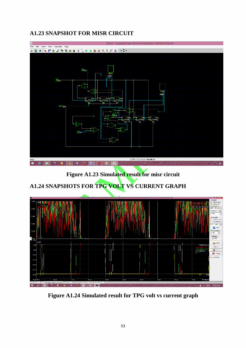
A1.23 SNAP SHOT FOR MISR CIRCUIT 53
A1.24 SNAP SHOT FOR TPG VOLT VS 53
CURRENT GRAPH
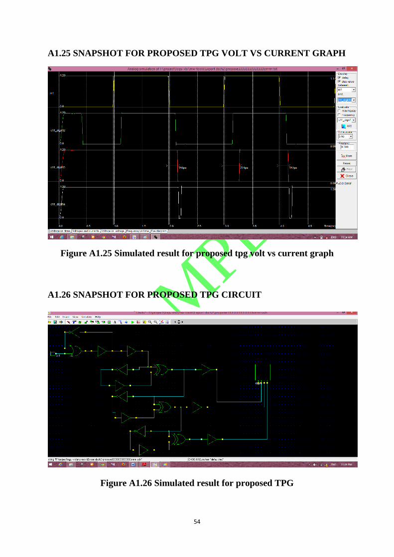
A1.25 SNAP SHOT FOR PROPOSED TPG 54
VOLT VS CURRENT GRAPH
A1.26 SNAP SHOT FOR PROPOSED TPG 54
REFERENCES 55

SAMPLE
LIST OF TABLES
TABLE
NO
TITLE PAGE
NO
1.1 Xor truth table 6
2.1 Truth table for modified clock 21
2.2 Total hamming distance reduction for 3BIT LFSR 22
3.1 Pattern produced by low power pattern generator 32
3.2 Checksum calculation 34
4.1 Performance analysis of different D flip flop
architectures
36
4.2 Total power consumption of conventional LFSR
and LFSR with modified clock
37
4.3 Comparison of average power between
conventional LFSR
37

SAMPLE
LIST OF FIGURES (Cont.…..)
FIGURE
NO
TITLE PAGE
NO
1.1 External testing using ATE 2
1.2 External (a)&(b) internal LFSR 4
1.3 Serial in serial out 4
1.4 Serial in parallel out 5
1.5 Parallel in serial out 5
1.6 Parallel in parallel out 6
1.7 Fibonacci LFSR 7
1.8 Test-per-clock configuration 9
1.9 Test-per-scan configuration 9
2.1 Test-per-clock design 12
2.2 Test pattern generator 15
2.3 LFSR with 16,14,13,11 bits 17
2.4 Exhaustive pattern generator block diagram 18
2.5 Multiple input signature register 20
2.6 Switching unit of LFSR 21
2.7 Proposed general modified TPG architecture 23
2.8 Model diagram of 12T DFF 28
2.9 Model diagram of 8T DFF 29
2.10 Model diagram of 5T DFF 29
SAMPLE
LIST OF FIGURES (Cont.…..)
FIGURE
NO
TITLE PAGE
NO
3.1 Block diagram for proposed model 30
3.2 Low power Pattern generator 31
3.3 Generation of test pattern 31
3.4 8 bit delay line 33
4.1 Normal test pattern generator 38
4.2 Asynchronous low power pattern generator 38
4.3 ORA circuit 39
4.4 ORA output 39
4.5 Comparison of synchronous and asynchronous
TPG
40
4.6 Comparison of existing ORA and proposed ORA 41
A1.1 Simulated result for pseudo random pattern 42
Generator
A1.2 Simulated result for exhaustive pattern generator 42
A1.3 Simulated result for external pattern generators 43
A1.4 Simulated result for low power D-FlipFlop 43
A1.5 Simulated result for low power proposed TPG 44
A1.6 Simulated result for low power existing TPG 44
A1.7 Simulated result for delay line 45
A1.8 Simulated result for fault free 45
A1.9 Simulated result for faulty 46
A1.10 Simulated result for existing layout 46

SAMPLE
LIST OF FIGURES (Cont.…..)
FIGURE
NO
TITLE PAGE
NO
A1.11 Simulated result for ORA layout 47
A1.12 Simulated result for layout 2 47
A1.13 Simulated result for layout 3 48
A1.14 Simulated result for full output 48
A1.15 Simulated result for proposed TPG 49
A1.16 Simulated result for adder 49
A1.17 Simulated result for delay line 50
A1.18 Simulated result for 10s proposed delay 50
A1.19 Simulated result for 10s existing 51
A1.20 Simulated result for existing TPG volt vs time 51
A1.21 Simulated result for misr tpg volt vs current graph 52
A1.22 Simulated result for misr tpg volt vs time graph 52
A1.23 Simulated result for misr circuit 53
A1.24 Simulated result for TPG volt vs current grap 53
A1.25 Simulated result for proposed tpg volt vs current 54
Graph
A1.26 Simulated result for proposed TPG circuit 54

SAMPLE
1
CHAPTER 1
INTRODUCTION
1.1 LOW POWER VLSI
Low power has emerged as a principal theme in today‟s electronics
industry. The need for low power has caused a major paradigm shift where
power dissipation has become as important a consideration as performance and
area. Our report reviews various strategies and methodologies for designing low
power circuits and systems. It describes the many issues facing designers at
architectural, logic, circuit and device levels and presents some of the
techniques that have been proposed to overcome these difficulties. The article
concludes with the future challenges that must be met to design low power, high
performance systems.
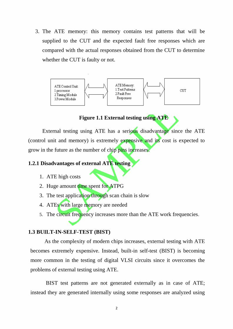
1.2 AUTOMATIC TEST EQUIPMENT (ATE)
Automatic test equipment (ATE) is instrumentation that is used in
external testing to apply test patterns to the CUT, to analyze the response from
the CUT and to mark the CUT as good or bad according to the analyzed
responses. Figure 1.2 shows basic diagram for external testing using ATE with
its three basic components:
1. The CUT: this is the integrated circuit (IC) part which is tested for
manufacturing defects.
2. The ATE control unit: this unit includes the control processor, the timing
module, and the power module.
SAMPLE
2
3. The ATE memory: this memory contains test patterns that will be
supplied to the CUT and the expected fault free responses which are
compared with the actual responses obtained from the CUT to determine
whether the CUT is faulty or not.
Figure 1.1 External testing using ATE
External testing using ATE has a serious disadvantage since the ATE
(control unit and memory) is extremely expensive and its cost is expected to
grow in the future as the number of chip pins increases.
1.2.1 Disadvantages of external ATE testing
1. ATE high costs
2. Huge amount time spent for ATPG
3. The test application through scan chain is slow
4. ATEs with large memory are needed
5. The circuit frequency increases more than the ATE work frequencies.
1.3 BUILT-IN-SELF-TEST (BIST)
As the complexity of modern chips increases, external testing with ATE
becomes extremely expensive. Instead, built-in self-test (BIST) is becoming
more common in the testing of digital VLSI circuits since it overcomes the
problems of external testing using ATE.
BIST test patterns are not generated externally as in case of ATE;
instead they are generated internally using some responses are analyzed using
SAMPLE
3
other parts of mode, test patterns generators (TPGs) generate patterns that are
applied to the CUT, while the output response analyzer (ORA) evaluates the
CUT responses. One of the most common TPGs for exhaustive, pseudo-
exhaustive, and pseudorandom TPG is the linear feedback shift register
(LFSR). LFSRs are used as TPGs for BIST circuits because, with little
overhead in hardware area, a normal register can be configured to work as a
test generator, and with an appropriate choice of the location of the XOR gates,
the LFSR can generate all possible output test vectors (with the exception of
the 0s-vector, since this will lock the LFSR). The pseudorandom properties of
LFSRs lead to high fault coverage when a set of test vectors is applied to the
CUT compared with the fault coverage obtained using normal counters as
TPGs. Also LFSRs can be configured to act as output response analyzers for
the responses obtained from the CUT. Despite their simple appearance, LFSRs
are based on complex mathematical theory that helps explain the behavior as
TPGs or ORAs.
The characteristic polynomial of an LFSR determines which flip-flop
locations of the LFSR feed the inputs of the XOR gates in the feedback path. If
the characteristic polynomial of an LFSR is primitive, then the LFSR will
generate the maximum length non-repeating sequence called an m-sequence.
LFSRs can be divided into two main categories: external-XOR LFSR (simply
external LFSR) and internal-XOR LFSR (simply internal LFSR). These are
distinguished by the way in which XOR gates are inserted into the system. In
an external LFSR only in the feedback, while in the internal LFSR the XORs
appear between flip-flops. As a simple example, the characteristic polynomial
p(x) = x3
+ x + 1 is a primitive polynomial of degree 3 (i.e. 3 flip-flops are
needed for implementation).

SAMPLE
4
Figure 1.2 External (a) & Internal (b) LFSRs
1.3.1 Serial in serial out (SISO)
Figure 1.3 Serial in serial out
A basic four-bit shift register can be constructed using four D flip-flops,
as shown below. The operation of the circuit is as follows. The register is first
cleared, forcing all four outputs to zero. The input data is then applied
sequentially to the D input of the first flip-flop on the left (FF0). During each
clock pulse, one bit is transmitted from left to right.
SAMPLE
5
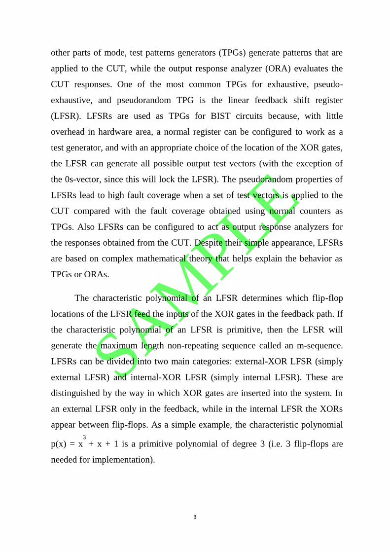
1.3.2 Serial in parallel out (SIPO)
Once the data has been input, it may be either read off at each output
simultaneously, or it can be shifted out and replace.
Figure 1.4 Serial in parallel out
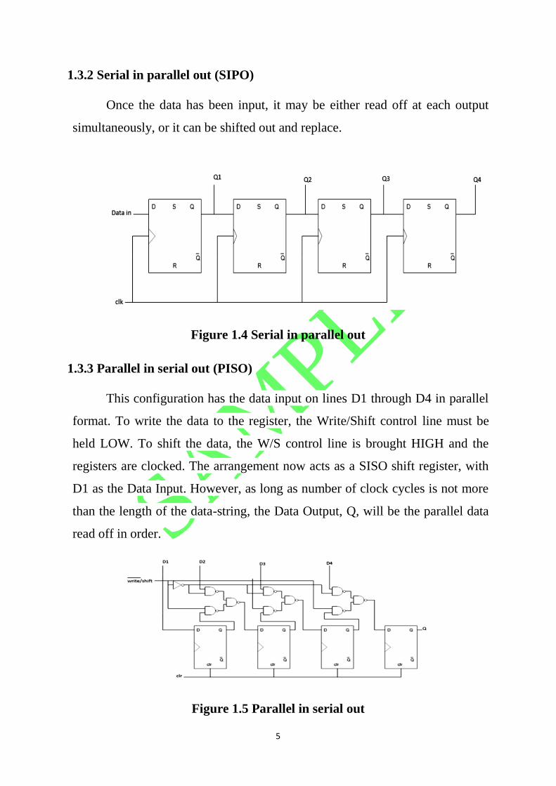
1.3.3 Parallel in serial out (PISO)
This configuration has the data input on lines D1 through D4 in parallel
format. To write the data to the register, the Write/Shift control line must be
held LOW. To shift the data, the W/S control line is brought HIGH and the
registers are clocked. The arrangement now acts as a SISO shift register, with
D1 as the Data Input. However, as long as number of clock cycles is not more
than the length of the data-string, the Data Output, Q, will be the parallel data
read off in order.
Figure 1.5 Parallel in serial out
SAMPLE
6
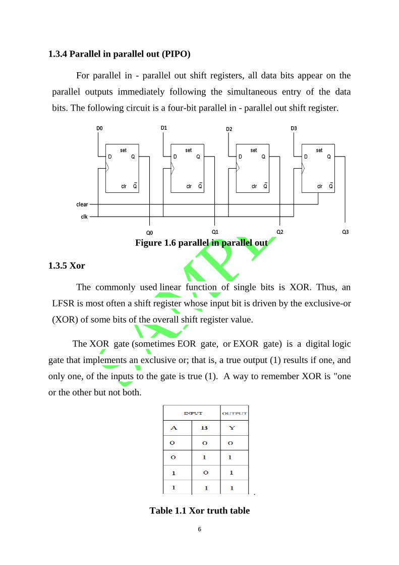
1.3.4 Parallel in parallel out (PIPO)
For parallel in - parallel out shift registers, all data bits appear on the
parallel outputs immediately following the simultaneous entry of the data
bits. The following circuit is a four-bit parallel in - parallel out shift register.
Figure 1.6 parallel in parallel out
1.3.5 Xor
The commonly used linear function of single bits is XOR. Thus, an
LFSR is most often a shift register whose input bit is driven by the exclusive-or
(XOR) of some bits of the overall shift register value.
The XOR gate (sometimes EOR gate, or EXOR gate) is a digital logic
gate that implements an exclusive or; that is, a true output (1) results if one, and
only one, of the inputs to the gate is true (1). A way to remember XOR is "one
or the other but not both.
.
Table 1.1 Xor truth table

SAMPLE
7
1.3.6 Fibonacci LFSR
Named after the French mathematician Évariste Galois, an LFSR in
Galois configuration, which is also known as modular, internal XORs as well
as one-to-many LFSR, is an alternate structure that can generate.
The same output stream as a conventional LFSR (but offset in time). In
the Galois configuration, when the system is clocked, bits that are not taps are
shifted one position to the right unchanged. The taps, on the other hand, are
XOR with the output bit before they are stored in the next position[8]. The new
output bit is the next input bit. The effect of this is that when the output bit is
zero all the bits in the register shift to the right unchanged, and the input bit
becomes zero. When the output bit is one, the bits in the tap positions all flip (if
they are 0, they become 1, and if they are 1, they become 0), and then the entire
register is shifted to the right and the input bit becomes 1.
To generate the same output stream, the order of the taps is
the counterpart of the order for the conventional LFSR; otherwise the stream
will be in reverse.
Figure 1.7 Fibonacci LFSR
A linear feedback shift register sequence is a pseudo-random sequence of
numbers that is often created in a hardware implementation of a linear feedback
shift register. A LFSR is an algorithm which yields a sequence of numbers
which is eventually periodic. When a LFSR is implemented in hardware, a
LFSR sequence is recursively generated by taking the output from the last stage
of a given LFSR to compute the next stage. This LFSR is of length , and each
state cell's current state is used as the input to the mod 2 adder. This adder is

SAMPLE
8
implemented in hardware with an exclusive-or function. Since this is a shift
register, each iteration of the register causes the state of each state cell to shift to
the next cell. We use the output of the last state cell to provide the next term of
the sequence after each iteration.
This hardware LFSR can be modeled mathematically to generate a LFSR
sequence. In order to build this sequence, three pieces of information are
needed. They are the key, the initial fill, and an algorithm to obtain the next
term of the sequence. In the hardware implementation, the connections between
the state cells and the mod 2 adder determines how the outputs of the cells are
used as inputs to the mod 2 adder. In the same way, the key determines how the
previous terms of the LFSR sequence are used to compute the next term in the
sequence. The key may be represented as a vector, but is more often defined by
a polynomial, known as the connection polynomial.
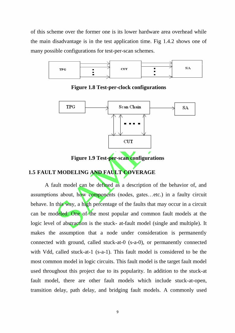
1.4 TEST-PER-CLOCK AND TEST-PER-SCAN
The BIST design methodology has been widely adopted in the design of
VLSI circuits in order to enable the chip to test itself and to evaluate its
response with an acceptable cost [5, 7]. BIST schemes can be divided into two
main types according to the way in which test patterns are applied to the CUT.
The first scheme is test-per-clock, in which the outputs of a TPG directly feed
the inputs of the CUT, and the outputs of the CUT are directly connected to an
SA. In this scheme a test vector is applied to the CUT, and a response is
captured from the CUT on each clock cycle. Fig 1.4.1 shows a test-per-clock
configuration. The second scheme is test-per-scan, in which a scan path is used
to shift test patterns into a CUT. A full scan cycle requires m+1 clock cycles,
where m is the number of flip-flops in the scan chain. The response to an
applied test pattern is captured into a scan chain and scanned out in the next
scan cycle in parallel with scanning in another test pattern. The main advantage
SAMPLE
9
of this scheme over the former one is its lower hardware area overhead while
the main disadvantage is in the test application time. Fig 1.4.2 shows one of
many possible configurations for test-per-scan schemes.
Figure 1.8 Test-per-clock configurations
Figure 1.9 Test-per-scan configurations
1.5 FAULT MODELING AND FAULT COVERAGE
A fault model can be defined as a description of the behavior of, and
assumptions about, how components (nodes, gates…etc.) in a faulty circuit
behave. In this way, a high percentage of the faults that may occur in a circuit
can be modeled. One of the most popular and common fault models at the
logic level of abstraction is the stuck- at-fault model (single and multiple). It
makes the assumption that a node under consideration is permanently
connected with ground, called stuck-at-0 (s-a-0), or permanently connected
with Vdd, called stuck-at-1 (s-a-1). This fault model is considered to be the
most common model in logic circuits. This fault model is the target fault model
used throughout this project due to its popularity. In addition to the stuck-at
fault model, there are other fault models which include stuck-at-open,
transition delay, path delay, and bridging fault models. A commonly used
SAMPLE
10
metric to represent the percentage of faults detected using a fault model is the
fault coverage (FC).
Where DF represents the number of detected faults, TF represents the
total number of faults in the CUT. However, most CUTs contain redundant
faults (RF) that are not detectable due to the presence of redundant hardware in
the circuit hence another way to represent fault coverage (EFC)
1.6 FAULT SIMULATION
In order to determine the fault coverage for a specified set of test vectors
applied to a CUT, fault simulation is carried out. For each fault expected in the
CUT (excluding redundant faults), the output produced when a test vector is
applied to a faulty circuit differs from the output produced in a fault-free
circuit. Thus, fault simulation produces a list of detected faults for each test
vector. There are many fault simulators that can be used for this purpose, some
commercial and others academic. The fault simulator that is predominantly
used within this thesis is an academic tool called FSIM [11] which is based on
parallel pattern single fault propagation for stuck-at faults defects.
SAMPLE
11
CHAPTER 2
LITERATURE SURVEY
2.1 EXISTING TECHNOLOGY
We have done a survey on the exhisting techniques in pattern
generator.Our survey on exhisting techniques are as follows
2.2 TEST PATTERN GENERATOR
The test pattern generator (TPG) consists of two parts: the pseudorandom
pattern generator (PRPG), which is usually an LFSR and the output decoder.
The output decoder is a combinational block transforming pseudorandom
vectors into deterministic test patterns pre-computed by an ATPG tool. The
method is designed for a test per-clock BIST, i.e., the test patterns are fed to the
circuit in parallel. Thus, the output decoder has as many inputs, as there are the
PRPG outputs (LFSR bits) and as many outputs as there are CUT inputs.
The earliest and most well-known fault model is the single stuck-at (SSA)
fault model (also called single stuck line(SSL) fault model), which assumes that
the defect will cause a line in the circuit to behave as if it is permanently stuck
at a logic value 0 (stuck-at-0) or 1 (stuck-at-1). This means that with the SSA
fault model it is assumed that the elementary components are fault-free and only
their interconnects are affected.
This will reduce the number of faults to 2n, where n is the number of
lines on which SSA faults can be defined. Experiments have shown that this
SAMPLE
12
fault model is useful (providing relatively high defect coverage, while being
technology-independent) and can be used even for identifying the presence of
multiple faults that can mask each other‟s impact on the circuit behavior.
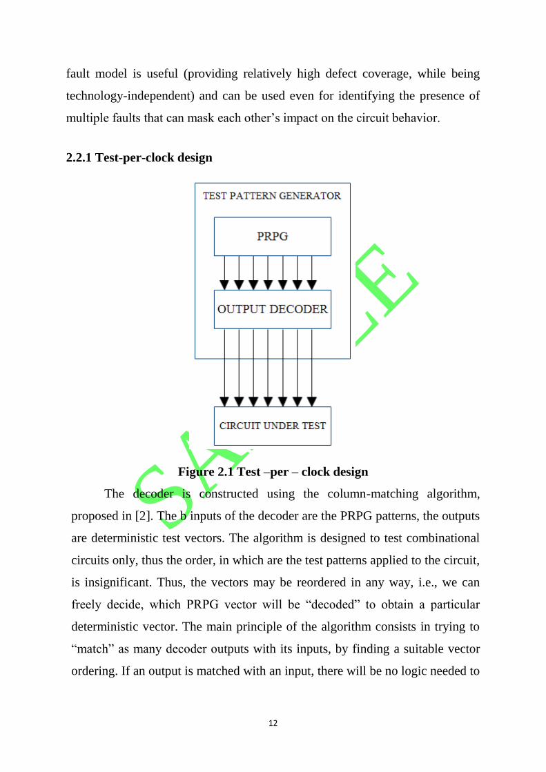
2.2.1 Test-per-clock design
Figure 2.1 Test –per – clock design
The decoder is constructed using the column-matching algorithm,
proposed in [2]. The b inputs of the decoder are the PRPG patterns, the outputs
are deterministic test vectors. The algorithm is designed to test combinational
circuits only, thus the order, in which are the test patterns applied to the circuit,
is insignificant. Thus, the vectors may be reordered in any way, i.e., we can
freely decide, which PRPG vector will be “decoded” to obtain a particular
deterministic vector. The main principle of the algorithm consists in trying to
“match” as many decoder outputs with its inputs, by finding a suitable vector
ordering. If an output is matched with an input, there will be no logic needed to

SAMPLE
13
implement this output; it will be implemented as a mere wire. Finding these
matches is a simple permutation problem.
Let us have an n-bit PRPG and an m-output CUT. The decoder will be
an n-input and m-output combinational block. There are n possibilities for a
column match for each of the m outputs. Thus, there are nm combinations to
test, to obtain an optimum matching. Such an algorithm complexity is
prohibitively large, thus some heuristic must be used instead of a brute force
approach. We use a thorough search algorithm, having an asymptotic=
complexity O (n·m2 ·p·s2), where p is the number of PRPG patterns and s the
number of deterministic vectors. For more details see .Then the algorithm has
been extended to support a mixed-mode BIST [4]. Here the BIST is divided in
to two phases: the pseudorandom and deterministic one. The difference
between our mixed-mode BIST method and the others is that the two phases
are disjoint. First, the easy-to-detect faults are covered in the pseudo-random
phase. Then, a set of deterministic test vectors covering the undetected faults is
computed and these tests are then generated by a transformation of the
subsequent PRPG patterns. This significantly reduces the decoder logic. A
general scheme of the column-matching mixed-mode BIST For sake of
simplicity the number of LFSR bits (and thus the Decoder inputs) was set
equal to the number of CUT inputs (m) here.
2.3 AUTOMATIC TEST PATTERN GENERATOR (ATPG)
The automatic test pattern generator (ATPG) is software dedicated to the
generation of test vectors that are used to detect the modeled faults in a CUT.
Since in many cases the generated vectors do not achieve 100% fault
coverage, the ATPG gives statistics about the FC achieved, the percentage of
redundant faults, and the aborted faults (which will therefore not be detected)
for these test vectors.

SAMPLE
14
Combinational ATPG is dedicated to generating test sets for
combinational circuits, or scan- ATPG tools can be divided into two types:
combinational ATPG and sequential ATPG. The based sequential circuits
where all of the state elements can be accessed directly through the scan-chain.
This ATPG, if it is well- designed, can generate test vectors that achieve high
fault coverage. Most of the combinational ATPGs depend on random and
deterministic phases in the generation of test vectors [1, 3].
In the random phase, the ATPG applies pseudo-random vectors to inputs
of the CUT and then performs fault simulation to check the fault coverage and
the faults remaining undetected. Normally, most of the faults are detected in
this phase. In the deterministic phase, the ATPG generates test vectors for
specific faults (that are hard to detect by pseudorandom means) and normally
uses algorithms such as the path sensitization method for this purpose.
The sequential ATPG, which is dedicated to the generation of test vectors
for sequential circuits, is more complicated as a result of the timing signals and
memory elements present in the circuit. In general, two test vectors are needed
to test a fault (or group of faults). The first test vector is used to initialize the
memory elements to a specified state, and then the next is used to detect the
presence of the fault(s). One of the aims of design for testability techniques is
to reduce the complexity of test generation for sequential circuits. One
common technique to achieve this is to change the sequential circuit to a scan-
based circuit.
In the random phase, the ATPG applies pseudo-random vectors to inputs
of the CUT and then performs fault simulation to check the fault coverage and
the faults remaining undetected. Normally, most of the faults are detected in
this phase. In the deterministic phase, the ATPG generates test vectors for

SAMPLE
15
specific faults (that are hard to detect by pseudorandom means) and normally
uses algorithms such as the path sensitization method for this purpose.
Figure 2.2 Test Pattern Generation
2.4 PSEUDO RANDOM PATTERN GENERATOR
LFSR is a shift register whose input bit is a linear function unlike most
everyday devices whose inputs and operations are effectively predefined, It is a
shift register that, when clocked moves the signal through the register from one
flip flop to next. Some of the outputs are combined in exclusive-OR
configuration to form a feedback mechanism. A LFSR can be formed by
performing exclusive-OR on the outputs of two or more of the flip-flops
together and feeding those outputs back into the input of one of the flip flops.

SAMPLE
16
The initial value of the LFSR is called the seed, and because the operation
of the register is deterministic, the sequence of values produced by the register
is completely determined by its current (or previous) state. Likewise, because
the register has a finite number of possible states, it must eventually enter a
repeating cycle. However, a LFSR with a well-chosen feedback function can
produce a sequence of bits which appears random in nature & which has a very
long cycle.
The list of bits position that affects the next state is called the tap
sequence. The outputs that influence the input are called taps. A maximal
LFSR produces an n-sequence (i.e. cycles through all possible 2n-1 states
within the shift register except the state where all bits are zero), unless it
contains all zeros, in which case it will never change. The sequence of numbers
generated by a LFSR can be considered a binary numeral system just as valid
as Gray code or the natural binary code.
2.4.1 Working of LFSR
Linear Feedback Shift Registers sequence through (2n-1) states, where
n is the number of registers in the LFSR. At each clock edge, the contents of the
registers are shifted right by one position. There is feedback from predefined
registers or taps to the left most register through an exclusive-NOR (XNOR) or
an exclusive-OR (XOR) gate. A value of all "1"s is illegal in the case of a
XNOR feedback. A count of all "0"s is illegal for an XOR feedback. This state
is illegal because the counter would remain locked-up in this state. The LFSR
shown below is implemented with XNOR feedback. A 4-bit LFSR sequences
through (24 - 1) = 15 states (the state 1111 is in the lock-up/illegal state). From
(Table 1) the feedback taps are 4, 3. On the other hand, a 4-bit binary up-
counter would sequence through 24 = 16 states with no illegal states. LFSR
counters are very fast since they use no carry signals.

SAMPLE
17
However, the dedicated carry in Vertex devices is rarely a speed limiting
factor because it is intrinsically fast. LFSRs can replace conventional binary
counters in performance critical applications where the count sequence is not
important (e.g., FIFO). LFSRs are also used as pseudo-random bit stream
generators. They are important building blocks in the implementation of
encryption and decryption algorithms. The list of the bits positions that affect
the next state is called the tap sequence. In the diagram below, the sequence is
(16, 14, 13,11).
The outputs that influence the input are called taps. A maximal LFSR
produces an n-sequence (i.e. cycles through all possible state within the shift
register), unless it contains all zeros, in which case it will never change.
The sequence of numbers generated by a LFSR can be considered a
binary numeral system just as valid as Gray code or the natural binary code. The
tap sequence of an LFSR can be represented as a polynomial mod 2. This means
that the coefficients of the polynomial must be 1's or 0's. This is called the
feedback polynomial or characteristic polynomial.
For example, if the taps are at the 16th, 14th, 13th and 11th bits (as
below), the resulting LFSR polynomial is x11 + x13 + x14 + x16 + 1
Figure 2.3 LFSR With 16,14,13,11 Bits
The 'one' in the polynomial does not correspond to a tap. The powers of
the terms represent the tapped bits, counting from the left.
If (and only if) this polynomial is a primitive, then the LFSR

SAMPLE
18
The LFSR will only be maximal if the number of taps is even.
The tap values in a maximal LFSR will be relatively prime.
There can be more than one maximal tap sequence
2.5 EXHAUSTIVE PATTERN GENERATOR
The generic pseudo-exhaustive two-pattern generator is consists of a
generic counter, 1‟s complement adder, a controller and a carry generator. The
7-bit pattern PE [7:1] is given as an input to the controller, generic counter and
C gen and the output A [7:1] is taken from the Accumulator. The operation of
the GPET varies based on the PE value. If the value PE 4 is enabled, a (7,3)-
pseudo-exhaustive test set is generated and a 3-bit exhaustive test set is applied
to the 2-bit groups A[3:1] ,A[6:4] , and a single bit test set is generated at A[7].
Figure 2.4 Exhaustive pattern generator block diagram
2.6 OUTPUT RESPONSE ANALYZER
The ORA compacts the output response of the CUT to the many test
patterns produced by the TPG into a single pass/fail indication (usually a
multiple-bit signature). The ORA is sometimes referred to as an output data
compaction circuit. The significance of the ORA is that there is no need to
compare every output response from the CUT with the expected output
response external to the device. Only the pass/fail indication needs to be

SAMPLE
19
checked at the end of the BIST sequence in order to determine the fault-
free/faulty state of the CUT.
2.7 TYPES OF ORA
2.7.1 One’s Count Compression method
The number of 1s in each output sequence are counted and compared
with the fault-free output of the CUT.
2.7.2 Transition Count Compression method
The number of transitions from 0 to 1 or from 1 to 0 are counted and
checked with the already known fault-free output of the circuit.
2.7.3 Parity Checking Compression method
The parity of each output sequence from the DUT is determined and
compared with the parity of the fault-free/good circuit. If they match, then
there is no error.
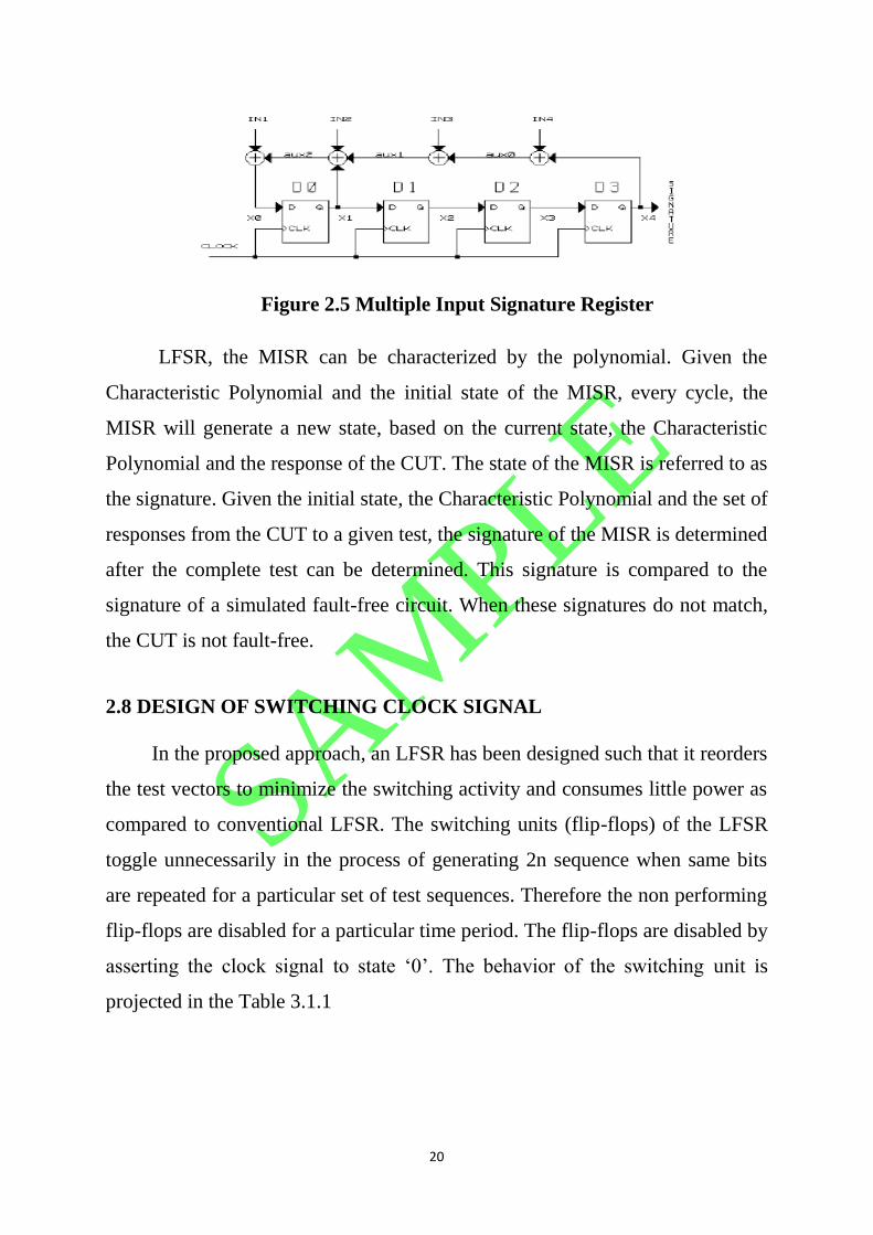
2.7.4 Signature Analysis Compression method
Signature analysis is performed only by Signature Register which is
similar in structure to LFSR. BIST requires ability to capture the test results
without the need for an external tester. This is often achieved by using a multi-
input signature register (MISR) to capture individual test results and compress
these into an overall value called the test signature. A MISR is quite similar to
an in-tapping LFSR, it consists of n memory cells (M1…Mn) with linear
feedbacks from cell Mn (n is the number of output of the CUT).
SAMPLE
20
Figure 2.5 Multiple Input Signature Register
LFSR, the MISR can be characterized by the polynomial. Given the
Characteristic Polynomial and the initial state of the MISR, every cycle, the
MISR will generate a new state, based on the current state, the Characteristic
Polynomial and the response of the CUT. The state of the MISR is referred to as
the signature. Given the initial state, the Characteristic Polynomial and the set of
responses from the CUT to a given test, the signature of the MISR is determined
after the complete test can be determined. This signature is compared to the
signature of a simulated fault-free circuit. When these signatures do not match,
the CUT is not fault-free.
2.8 DESIGN OF SWITCHING CLOCK SIGNAL
In the proposed approach, an LFSR has been designed such that it reorders
the test vectors to minimize the switching activity and consumes little power as
compared to conventional LFSR. The switching units (flip-flops) of the LFSR
toggle unnecessarily in the process of generating 2n sequence when same bits
are repeated for a particular set of test sequences. Therefore the non performing
flip-flops are disabled for a particular time period. The flip-flops are disabled by
asserting the clock signal to state „0‟. The behavior of the switching unit is
projected in the Table 3.1.1
SAMPLE
21
Table 2.1 Truth table for modified clock
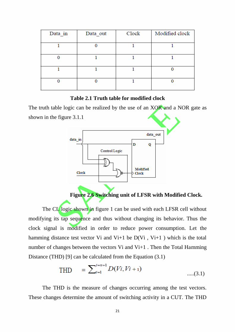
The truth table logic can be realized by the use of an XOR and a NOR gate as
shown in the figure 3.1.1
Figure 2.6 Switching unit of LFSR with Modified Clock.
The CL logic shown in figure 1 can be used with each LFSR cell without
modifying its tap sequence and thus without changing its behavior. Thus the
clock signal is modified in order to reduce power consumption. Let the
hamming distance test vector Vi and Vi+1 be D(Vi , Vi+1 ) which is the total
number of changes between the vectors Vi and Vi+1 . Then the Total Hamming
Distance (THD) [9] can be calculated from the Equation (3.1)
.....(3.1)
The THD is the measure of changes occurring among the test vectors.
These changes determine the amount of switching activity in a CUT. The THD

SAMPLE
22
can be minimized if test vectors are shifted in a proper order. The LFSR with
control logic is used along with a reordering algorithm based on bit
interchanging method in [5]. In an n-bit LFSR with bits 1, 2, 3, 4…q, q+1, n, if
the bit n (the selection bit) has a value „0‟ (or „1‟) the interchanging is
performed between bit 1 & bit 2, between bit 3 & bit 4 and so on. If bit n has a
value of 1(or 0) then no interchanging is performed. The process ultimately
generates a new order of test vectors[10]. Let us illustrate the point with an
example. We have a set of test vectors generated from a maximal length 3-bit
LFSR. Applying the bit interchanging methodology a new order of the same
test vectors is obtained. The resultant reduction in the hamming distance is
depicted in the Table 3.1.2.
Table 2.2 Total hamming distance reduction for 3-BIT LFSR

SAMPLE
23
Here a case of odd n is considered. When n is even the
interchanging is performed up to third and fourth last FF outputs. Embedding
the Bit Interchanging Module with the modified clock LFSR makes the design
more power efficient as in Figure 3.1.2.
In this architecture the CL block contains the XOR and NOR logic for
controlling the clock as shown in Figure. 2.7. The output from the LFSR is
passed to the bit inter-changing module which constitutes of multiplexers. It
interchanges the bits as per the proposed methodology and finally generates a
set of reordered test vectors.
Figure 2.7 Existing general Modified TPG Architecture
2.9 DESIGN OF LOW POWER FLIP-FLOP
2.9.1 Leakage power analysis
We have different types of leakage components. They are

SAMPLE
24
1. Sub-threshold leakage (weak inversion current)
2. Gate oxide leakage (Tunneling current)
3. Channel punch through
4. Drain induced barrier lowering
2.9.1.1 Sub Threshold Leakage
One of the main reasons causing the leakage power increase is increase
of sub threshold leakage power. The Sub-threshold conduction or the sub-
threshold leakage or the sub threshold drain current is the current that flows
between the source and drain of a MOSFET when the transistor is in sub-
threshold region, or weak-inversion region, that is, for gate-to source voltages
below the threshold voltage. The sub-threshold region is often referred to as the
weak inversion region. When technology feature size scales down, supply
voltage and threshold voltage also scale down. Sub-threshold leakage power
increases exponentially a sub threshold voltage decreases which increases the
sub-threshold leakage power Sub threshold or weak inversion conduction
current between source and drain in a MOS transistor occurs when gate voltage
is below the transistor threshold voltage (Vt). The Sub threshold or weak
inversion current (Ids) can be and is threshold voltage and is the thermal
voltage. is the gate oxide capacitance, is the zero bias mobility and is the body
effect coefficient. Is the maximum depiction layer width and is the gate oxide
thickness is the capacitance of the depletion layer. Reverse biasing well to
source junction of a MOSFET widens the bulk depletion region and increases.
2.9.1.2 The Gate Oxide Leakage
The gate oxide, which serves as insulator between the gate and channel,
should be made as thin as possible to increase the channel conductivity and
performance. But as the gate oxide is made thinner the barrier voltage of the
oxide changes. For the positive gate voltage thus some positive charges get

SAMPLE
25
stuck in the oxide.Therefore, current flows through the oxide. This is also
known as tunneling current.
2.9.1.3 Channel Punch Through
Punch through in a MOSFET is an extreme case of channel length
modulation where the depletion layers around the drain and source regions
merge into a single depletion region. The field underneath the gate then
becomes strongly dependent on the drain-source voltage, as is the drain current.
Punch through causes a rapidly increasing current with increasing drain-source
voltage. This effect is undesirable as it increases the output conductance and
limits the maximum operating voltage of the device
2.10 REVIEW OF LEAKAGE CURRENT
2.10.1 Reduction techniques
For a CMOS circuit, the total power dissipation includes dynamic and
static components during the active mode of operation. In the standby mode, the
power dissipation is due to the standby leakage current. Dynamic power
dissipation consists of two components. One is the switching power due to
charging and discharging of load capacitance. The other is short circuit power
due to the nonzero rise and fall time of input waveforms. The static power of a
CMOS circuit is determined by the leakage at the circuit level.
2.10.2 Sleep transistor approach
In previous MTCMOS approach, sleep and sleep bar transistors of high
threshold voltages are inserted in series between the circuit and VDD and
ground due to this high threshold voltage the additional delay will add to the
main circuit so in sleep transistor approach we use same threshold voltage to
sleep transistors When sleep input is OFF and sleep bar input is ON, there is no
current flow in the low threshold voltage main circuit. When sleep is ON and

SAMPLE
26
sleep bar is OFF then the circuit works in normal mode, the sleep transistor
technique dramatically reduces leakage power during sleep mode. , the
additional sleep transistors increase area and delay but it is low compare to
MTCMOS.
2.10.3 Sleepy stack approach
The sleepy stack approach uses sleep transistor and the stacked transistor
in each network are made parallel. Here the width of the sleep transistors is
reduced. . The activity of the sleep transistors in sleepy stack is same as the
activity of the sleep transistors in the sleep transistor technique.[3] The sleep
transistors are turned on during active mode and turned off during sleep mode. .
The high Vth transistors are used for the sleep transistor and the transistors
parallel to the sleep transistor without incurring large delay increase. The delay
time is increase sing here but it gives low leakage. During sleep mode both the
sleep transistors are turned off. But the sleepy stack structure maintains exact
logic state.
2.10.4 Dual sleep approach
In dual sleep method two sleep transistors in each NMOS or PMOS
block are used. One sleep transistor is used to turn on in ON state and the other
one is used to turn on in OFF state. Dual sleep approach uses the advantage of
using the two extra pull-up and two extra pull- down transistors in sleep mode
either in OFF state or in ON state. It uses two pull-up sleep transistors and two
pull-down sleep transistors. When S=1 the pull down NMOS transistor is ON
and the pull-up PMOS transistor is ON since S‟=0. So the arrangement works
as a normal device in ON state. During OFF state S is forced to 0 and hence the
pull down NMOS transistor is OFF and PMOS transistor is ON and the pull-up
PMOS transistor is OFF while NMOS transistor is ON. So in OFF state a

SAMPLE
27
PMOS is in series with an NMOS both in pull-up and pull-down circuits which
is liable to reduce power.[1]
2.10.5 Dual stacked sleep approach
This technique uses two stacked sleep transistor in Vdd and two stacked
sleep transistor in ground. So, leakage reduction in this technique occurs in two
ways. First, the stack effect of sleep transistors and second, the sleep transistor
effect. It is well known that p-mos transistors are not efficient at passing GND;
similarly, it is well known that n-mos transistors are not efficient at passing
Vdd. But this stacked sleep technique uses pmos transistor in GND and n-mos
transistor in Vdd for maintaining the exact logic state during sleep mode The
extra two transistors of the design for maintaining the logic state during sleep
mode.
2.11 ADVANCE APPROACHES
2.11.1 Sleepy keeper approach
The sleepy keeper circuit maintains output value of “1” and an NMOS
transistor continues this value during sleep mode [6]. An additional NMOS
transistor is added in parallel to the pull up sleep transistor connected to Vdd. In
sleep mode this NMOS transistor is the only source of Vdd to the pull-up
network since the sleep transistor is off. Similarly, to maintain a “0” value, The
sleepy keeper approach maintain output value of “0” and a PMOS transistor
maintains the value during sleep mode .An additional PMOS transistor is added
in parallel to the pull down sleep transistor connected to GND. At sleep mode
this PMOS transistor is only source of GND the pull down network since the
sleep transistor is off. The draw backs of sleepy keeper are that it consumes
31% more dynamic power than the sleepy stack.

SAMPLE
28
2.11.2 Forced sleepy approach
The forced sleep method has a structure merging the forced stack
technique and the sleep transistor technique, uses W/L = 3 for the pmos
transistors and W/L = 1.5 for the n-mos transistors, ld use W/L = 6 for the pull-
up transistor and W/L = 3 for the pull down transistor (assuming μn = 2μp).
Then sleep transistors are added in series to each set of two stacked transistors.
We use two sleep transistors here, the n-mos sleep transistor with Vdd and the
pmos sleep transistor with ground. Conventionally the n-mos transistor is
connected to ground because it is very efficient passing ground voltage and the
pmos transistor is connected to Vdd because it is efficient passing Vdd In forced
sleep method we just reverse the connection.That‟s why we have some delay
penalty in our method. We use same W/L for all the pmos and nmos transistors.
Figure 2.8 Model Diagram of 12t DFF
SAMPLE
29
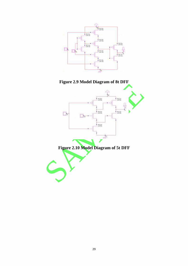
Figure 2.9 Model Diagram of 8t DFF
Figure 2.10 Model Diagram of 5t DFF

SAMPLE
30
CHAPTER 3
PROPOSED TECHNIQUE
3.1 BLOCK DIAGRAM OF PROPOSED MODEL
In this proposed approach there are three major blocks. They are low
power pattern generator, device under test, output response analyzer and in
addition to this we have delay line .The operations of each block are mentioned
below. The block diagram of our proposed approach is shown in figure 3.1
Figure 3.1 block diagram for proposed model
3.2 LOW POWER PATTERN GENERATOR
In existing technique D FLIPFLOP are used for generating test pattern
but in our approach we has been replaced all the D FLIPFLOP with buffers,
similarly in previous technique the test pattern generator is of synchronous type
,in this proposed approach the test pattern generator has been designed as
asynchronous type
Output response analyser (ORA)

SAMPLE
31
Figure 3.2 Low power pattern generator
In this model the delay of the buffer is design such a way that is explain in
following steps
STEP 1:A test pattern generator can generate up to 2^ n patterns .Here the 8
pattern are splited in column wise because we are designing 3 bit test pattern
generator as shown in figure..
STEP 2: Consider the column 1.The pattern remains 0 for first 4 pattern and
becomes high in next 4 pattern
STEP 3: In second column the pattern remain 0 for first 2 patterns and then it
became high for next two pattern (i.e) when the zero state of first column is
divided by half and one half is set as high and other half is set as low.
STEP 4: Similarly for third column the zero state of second column is divided
by half and one half is set as high and other half is set as low. Similarly, it is
done for high state also.
Figure 3.3 Generation of test patterns

SAMPLE
32
When the above circuit is given to display the output is as follows
Column 1 Column 2 Column 3
0 0 0
0 0 1
0 1 0
0 1 1
1 0 0
1 0 1
1 1 0
1 1 1
Table 3.1 Pattern produced by low power pattern generator
3.3 OUTPUT RESPONSE ANALYSER
In the proposed approach, the pattern generated from low power test
pattern generator is much faster than other test pattern generators. The generated
pattern is applied to the device under test .The pattern that comes from the
device under test is faster when compare with other type of MISR. So, we can‟t
use normal MISR. So we go for technique “error detection using
CHECKSUM” method .In order to apply this technique, the pattern has to be
divide into 8 bit pattern, this is because a 3 bit test pattern generator produce 8
bits when applied to device under test. The pattern coming from the device
under test is in continuous range .In order to divide the pattern into 8 bit pattern
equally an 8 bit delay line is used .The delay line is constructed using eight D
FLIPFLOP and eight 2 : 1 mux as shown in the figure 3.4. The delay line
timing diagram is shown in the figure 3.4..From the figures 3.3 it shows that
each bit from the device under test is shifted and 8 bit are taken separately. This
is done by adjusting the delay of the d flip flop such that the 8 bit pattern
reaches the adder of checksum techniques at same time without any mismatch

SAMPLE
33
in their delay. Suppose if there is any delay mismatch in the delay line then
there will be mismatch in the expected output.
Figure 3.4 8-Bit Delay line
3.4 CHECKSUM TECHNIQUE
A 8 bit pattern has been separated using the proposed delay line method.
This 8 bit pattern is divided into two parts such that the first 4 bit is added with
the next 4 bit. In order to perform addition operation we go for a simple 4 bit
carry propagation adder. The output of the adder is complemented using NOT
gate. Next step is to add the 4 bit pattern before complementing and the 4 bit
pattern after complementing using 8 bit carry propagation adder. If the result is
F(1111) then the device which is under test is an error free device. If the result
is other than the result obtain then the device is an error one. This can be
verified by adding the 8 bit error pattern from the device and the result is added
with the previous complemented pattern of error free device .the result of the
resultant pattern will definitely not equal to F(1111).

SAMPLE
34
FAULT FREE
DEVICE
FAULTY DEVICE
PATTERN
PRODUCED FROM
THE DEVICE UNDER
TEST
00101101 00001101
Error bit
0010 0000
1101 1101
ADDITION 1111 1101
COMPLEMENT 0000 0000
RESULT 1111(F) 1101
Table 3.2 Checksum calculation
SAMPLE
35
CHAPTER 4
RESULTS AND PERFORMANCE ANALYSIS
4.1 PERFORMANCE ANALYSIS OF DIFFERENT D FLIPFLOP
In this, performance analyses of different D-Flip-flop Circuits are
presented, proposed 5t DFF has low power consumption compare to all other
DFF, the Efficiency of Power reduction varies with different topology with
different leakage reduction technique. Best average power reduction pavg
(30%) and peak(99.90%) is reported with sleep transistor technique, due to its
power gating ability.Lowest Power (0.301uw)) is reported ,and sleepy keeper
and forced sleep also gives better results. the election of leakage power
reduction technique is depends upon topology and designing technology of DFF
The techniques available so far have focused upon reducing the switching
activity from the test patterns generated from the generator. Embedding the
switching activity minimizing techniques with a power efficient test pattern
generators will be a good step ahead. Therefore a modification is proposed in
the conventional LFSR by embedding it with control logic module and bit
interchanging module. This culminates into a novel architecture of the test
pattern generator (TPG). The modified TPG architecture is capable of not only
disabling the switching units for a particular time frame but also reorders the
test vectors so as to reduce the transition activity. The benefit of the proposed

SAMPLE
36
TPG is that it can be used with any other low power technique to have further
reduction in power.
CIRCUIT POWER(uw) DELAY(ns) PDP(fj) AREA(um)
BASE
CSAE
0.418 0.052 0.021 40
SLEEP
TRANSISTOR
0.301 4.028 1.513 60
SLEEPY
STACK
0.420 1.028 0.438 72
DUAL
SLEEP
0.375 1.425 0.605 72
DUAL
STACK
0.378 1.029 1.019 105
SLEEPY
KEEPER
0.322 4.017 1.293 72
FORCED
SLEEP
0.304 4.018 1.221 84
Table 4.1 Performance analysis of different D flip flop Architectures
4.2 TOTAL POWER CONSUMPTION OF CONVENTIONAL LFSR
AND LFSR WITH MODIFIED CLOCK
In order to analyze the power reduction from the proposed TPG
architecture, we have evaluated the power consumption in 8 bit conventional
LFSR and 8 bit LFSR with modified clock for same input vector and same
clock cycles. Experiments were performed Xilinx ISE 9.2i plate form and total
power consumption was calculated using X power. The result of Table 3, shows
that the disabling the flip-flops for a time period when they are not performing,
leads to reduction in total power consumption up to 10%. The obtained results
from Table 5 show the decrease in average power calculated on the basis of
weighted transition activity. The reduction in average power depends upon the
tap sequences of the maximal length LFSR. Two approaches for indicating the
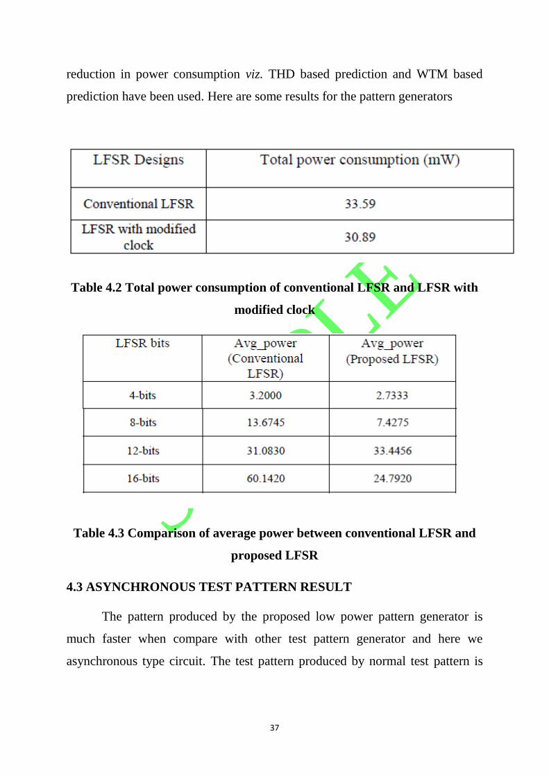
SAMPLE
37
reduction in power consumption viz. THD based prediction and WTM based
prediction have been used. Here are some results for the pattern generators
Table 4.2 Total power consumption of conventional LFSR and LFSR with
modified clock
Table 4.3 Comparison of average power between conventional LFSR and
proposed LFSR
4.3 ASYNCHRONOUS TEST PATTERN RESULT
The pattern produced by the proposed low power pattern generator is
much faster when compare with other test pattern generator and here we
asynchronous type circuit. The test pattern produced by normal test pattern is
SAMPLE
38
shown in the figure 4.1 and the output produced by the proposed low power
pattern generator is shown in the figure 4.2
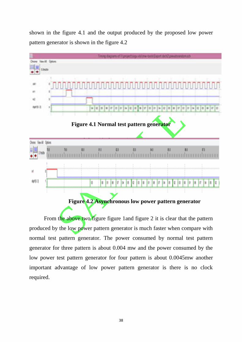
Figure 4.1 Normal test pattern generator
Figure 4.2 Asynchronous low power pattern generator
From the above two figure figure 1and figure 2 it is clear that the pattern
produced by the low power pattern generator is much faster when compare with
normal test pattern generator. The power consumed by normal test pattern
generator for three pattern is about 0.004 mw and the power consumed by the
low power test pattern generator for four pattern is about 0.0045mw another
important advantage of low power pattern generator is there is no clock
required.

SAMPLE
39
4.4 OUTPUT RESPONSE ANALYSER RESULT
The overall block diagram of the proposed model is given below in the figure
4.3
Figure 4.3 ORA circuit
Figure 4.4 ORA output

SAMPLE
40
The above figure shows the result of the proposed model.the last timing
diagram which is of green color shows the output for an error free circuit which
is F(1111) and the last above timing diagram shows the output for an error
circuit ,which produces the pattern other than F(1111). The chart shows that
normal test pattern generator proposed model is 50 percent faster higher
switching activity when compared with normal test pattern generator .
4.5 COMPARISON OF SYNCHRONOUS AND ASYNCHRONOUS TPG
The synchronous test pattern generator circuit needed clock to produce
pattern generator, but asynchronous test pattern generator doesn‟t needed any
clock to produce test pattern.
Figure 4.5 Comparison of synchronous and asynchronous TPG
0
20
40
60
80
100
120
140
160
180
number of pattern generated for 10 sec
normal pattern generator
proposed pattern generator
SAMPLE
41
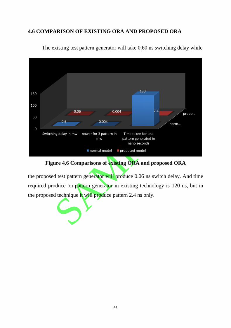
4.6 COMPARISON OF EXISTING ORA AND PROPOSED ORA
The existing test pattern generator will take 0.60 ns switching delay while
Figure 4.6 Comparisons of existing ORA and proposed ORA
the proposed test pattern generator will produce 0.06 ns switch delay. And time
required produce on pattern generator in existing technology is 120 ns, but in
the proposed technique it will produce pattern 2.4 ns only.
norm…
propo…
0
50
100
150
Switching delay in mw power for 3 pattern inmw
Time taken for onepattern generated in
nano seconds
0.6 0.004
130
0.06 0.004 2.4
normal model proposed model

SAMPLE
42
APPENDIX 1
A1.1 SNAPSHOT FOR PSEUDO RANDOM PATTERN GENERATORS
Figure A1.1 Simulated result for pseudo random pattern generator
A1.2 SNAPSHOT FOR EXHAUSTIVE PATTERN GENERATORS
Figure A1.2 Simulated result for exhaustive pattern generator

SAMPLE
43
A1.3 SNAPSHOT FOR EXTERNAL PATTERN GENERATORS
Figure A1.3 Simulated result for external pattern generators
A1.4 SNAPSHOT FOR LOW POWER D-FLIPFLOP
Figure A1.4 Simulated result for low power D-Flipflop

SAMPLE
44
A1.5 SNAPSHOT FOR PROPOSED TPG
Figure A1.5 Simulated result for proposed TPG
A1.6 SNAPSHOT FOR EXISTING TPG
Figure A1.6 Simulated result for existing TPG
SAMPLE
45
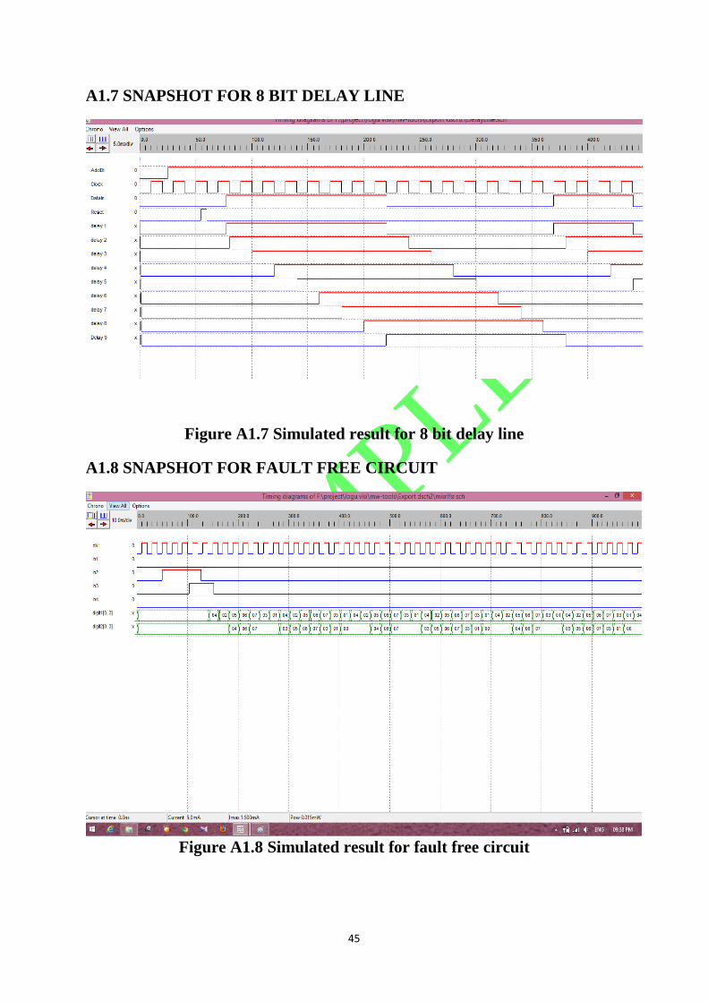
A1.7 SNAPSHOT FOR 8 BIT DELAY LINE
Figure A1.7 Simulated result for 8 bit delay line
A1.8 SNAPSHOT FOR FAULT FREE CIRCUIT
Figure A1.8 Simulated result for fault free circuit
SAMPLE
46
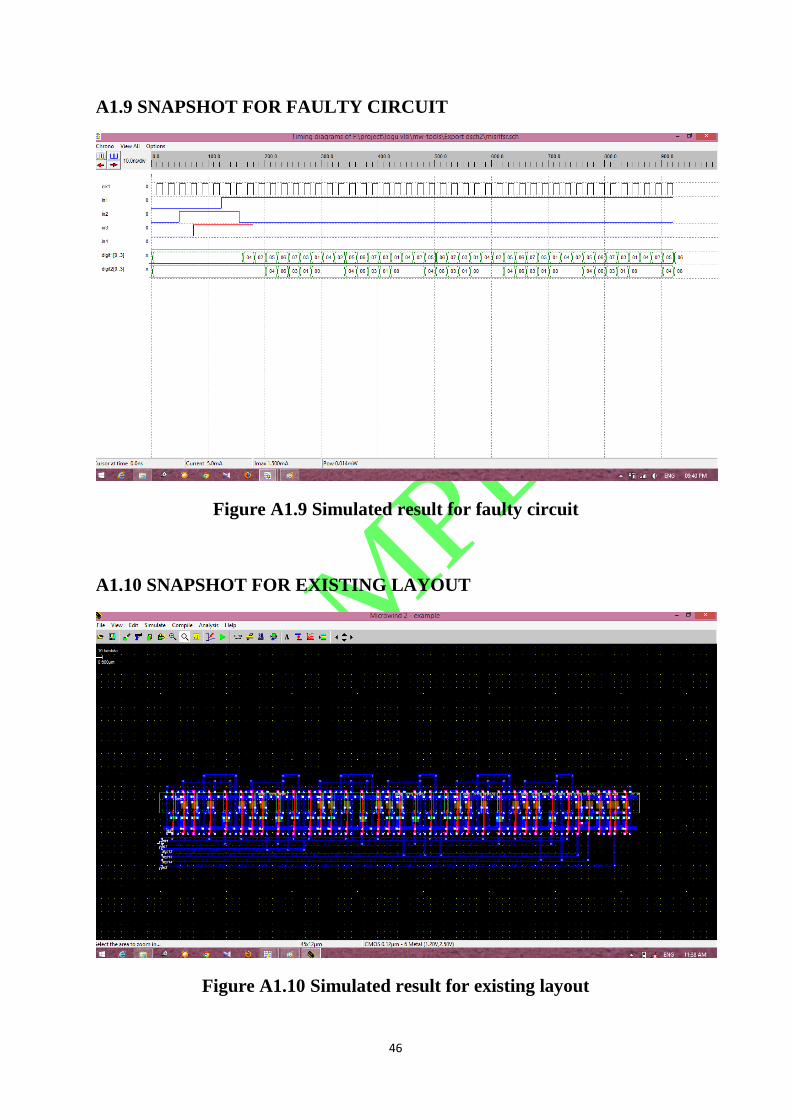
A1.9 SNAPSHOT FOR FAULTY CIRCUIT
Figure A1.9 Simulated result for faulty circuit
A1.10 SNAPSHOT FOR EXISTING LAYOUT
Figure A1.10 Simulated result for existing layout

SAMPLE
47
A1.11 SNAPSHOT FOR ORA LAYOUT 1
Figure A1.11 Simulated result for ORA layout 1
A1.12 SNAPSHOT FOR LAYOUT 2
Figure A1.12 Simulated result for layout 2

SAMPLE
48
A1.13 SNAPSHOT FOR LAYOUT 3
Figure A1.13 Simulated result for layout 3
A1.14 SNAPSHOT FOR PROPOSED OUTPUT
Figure A1.14 Simulated result for proposed output
SAMPLE
49
A1.15 SNAPSHOT FOR PROPOSED TPG LAYOUT
Figure A1.15 Simulated result for proposed TPG layout
A1.16 SNAPSHOT FOR 8 BIT ADDER
Figure A1.16 Simulated result for 8 bit adder
SAMPLE
50
A1.17 SNAPSHOT FOR 8 BIT DELAY LINE USING MICROWIND
Figure A1.17 Simulated result for 8 bit delay line using microwind
A1.18 SNAPSHOT FOR PROPOSED TPG (10 S)
Figure A1.18 Simulated result for proposed TPG (10s)
SAMPLE
51
A1.19 SNAPSHOT FOR EXISTING MODEL (10 S)
Figure A1.19 Simulated result for existing model (10s)
A1.20 SNAPSHOT FOR EXISTING TPG VOLT VS TIME GRAPH
Figure A1.20 Simulated result for existing TPG volt vs time
SAMPLE
52
A1.21 SNAPSHOT FOR MISR TPG VOLT VS CURRENT GRAPH
Figure A1.21 Simulated result for misr tpg volt vs current graph
A1.22 SNAPSHOT FOR MISR TPG VOLT VS TIME GRAPH
Figure A1.22 Simulated result for misr tpg volt vs time graph
SAMPLE
53
A1.23 SNAPSHOT FOR MISR CIRCUIT
Figure A1.23 Simulated result for misr circuit
A1.24 SNAPSHOTS FOR TPG VOLT VS CURRENT GRAPH
Figure A1.24 Simulated result for TPG volt vs current graph
SAMPLE
54
A1.25 SNAPSHOT FOR PROPOSED TPG VOLT VS CURRENT GRAPH
Figure A1.25 Simulated result for proposed tpg volt vs current graph
A1.26 SNAPSHOT FOR PROPOSED TPG CIRCUIT
Figure A1.26 Simulated result for proposed TPG

SAMPLE
55
REFERENCES
1. Abu-Issa, A.S. and Quigley, S.F. (2008) „Bit Swapping LFSR for low-
power BIST‟, IEEE Transactions on Electronics Computer Technology
vol.44, pp.401-402.
2. Blinder Singh, ArunKhosla and SukhleenBindra (2009) „Power
Optimization of Linear Feedback Shift Register (LFSR) for Low Power
BIST‟, IEEE Transactions on Advanced Computing, pp.311-314.
3. Boye and Tian-wang Li (2010) „A Novel BIST Scheme for Low Power
Testing‟, IEEE Transactions on Computer Science and Information
Technology, Vol.53, No.1, pp.134-137.
4. Jha, N.K. and Gupta,S. (2003) „Testing of Digital Systems‟, Cambridge
University Press.
5. Laung-Terng Wang, Cheng-Wen Wu and Xiaoqing Wen (2006) „Vlsi
Test Principles And Architectures Design For Testability‟, Academic
Press.
6. ManoharAyinala and Keshab K. Parhi (2011) „High-Speed Parallel
Architectures for Linear Feedback Shift Registers‟, IEEE Transactions
On Signal Processing, vol. 59, pp. 4459-4469.
7. Miron Abramovici, Melvin A.Breuer and Arthur D.Friedman
(1990) „Digital Systems Testing and Testable Design‟, IEEE Press.
8. Pong P. Chu and Robert E. Jones (2010) „Design Techniques of FPGA
Based Random Number Generator‟, paper presented at NASA Glen
Research Center,Cleveland,Ohio.

SAMPLE
56
9. Saraswathi,T., Ragini,K. and Ganapathy Reddy,Ch. (2011) „A Review on
Power optimization of Linear Feedback Shift Register (LFSR) for Low
Power Built In Self Test (BIST)‟, IEEE Transactions on Electronics
Computer Technology, Vol.6, pp.172-176.
10. Tomoaki Sato Rena Sakuma, Daisuke Miyamori, and Masa-akiFukase
(2005) „Waved-PRNG for a Wave-Pipelining Test Circuit‟, 12th NASA
Symposium on VLSI Design.