samtec whitepaper
TRANSCRIPT

DesignCon 2012
Connector Models – Are they any good?
Jim Nadolny, Samtec [email protected] Leon Wu, Samtec [email protected]

Abstract Channel simulations are only as accurate as the models used to develop them. While we have seen much effort placed on printed circuit board (PCB) materials (copper finish, dielectric moisture absorption), other elements within the channel have been largely ignored. In this paper, we look at the variation in performance of a high density connector including insertion depth, return path via location and solder variations. Model validation using measurements is only possible if the reference plane locations are common between the measurement and model. Measurement details including the impact of calibration structure on correlation are presented. Model quality metrics using Feature Selective Validation (FSV) and Model Quality Factor (MSF) are also introduced.
Author(s) Biography Jim has an MSEE from the University of New Mexico and is the author of more than 20 publications on SI and EMI topics. He has more than 15 years in the connector industry and is a frequent contributor to DesignCon with paper awards in 2004 and 2008. At Samtec, he leads Global SI efforts. Leon has 7 years of industry experience as an SI engineer having worked for FCI, Flextronics and Samtec. He is currently pursuing his PhD from the National Taipei University of Technology. Leon manages the SI Lab at Samtec’s Huizhou facility which focuses on connector measurements, and he also performs full wave simulations which support research efforts. He has 6 patents related to connector/footprint design and has published on novel termination methods for memory interfaces.
Introduction Connector models have evolved from simple lumped element representations to coupled multiport microwave models. This evolution parallels the growing sophistication of channel analysis driven by increased data rates. And while the performance of modern high speed connectors has improved, connectors remain the dominant mechanism for reflection loss and crosstalk in typical PCB based channels. In this paper, we will look at the performance variation of modern, high density connector models. Models will be derived both from simulation and measurements and subsequently compared. Real world variations due to incomplete insertions and soldering effects will be considered. Finally, model quality metrics will be applied to the data to quantify the accuracy of the models.

Evolution of Connector Models Connector models have evolved from simple lumped element representations to multi-port microwave networks. This complexity increase is driven by the need to accurately represent a complex geometric discontinuity over an ever increasing bandwidth. The earliest models of connectors were a single lumped element. These models are very simple, run quickly in simulation software and are still in use today for many applications. The generally accepted rule of thumb is that a lumped element representation of a transmission line is valid so long as the transmission line length (L) is less than one tenth of the wavelength (L<λ/10). To illustrate this point, consider a 1 inch length of 25 ohm transmission line in a 50 ohm system. We can model that 25 ohm transmission line as a 5 pF capacitor as shown in the schematic below:
Figure 1. Lumped Element Model of a Low Impedance Transmission Line
Using the rule of thumb L<λ/10, we would expect this 5 pF model to be accurate up to about 600 MHz. Figure 2 shows the results of the analysis and it is clear that this is a fairly conservative rule of thumb. The point of this example is to show the bandwidth limitations of a lumped element modeling approach. The logical extension of a single lumped element model is a distributed element model. The transmission line is divided into multiple smaller sections, and the model bandwidth can be easily extended.

Figure 2. Bandwidth Limitation of Lumped Element Model
This relationship can be expressed in the time domain as well by the following equation:
∗ 6 [1]
This equation says that a lumped element modeling method is valid so long as the propagation delay of the connector (tprop delay) is greater than 6 times the system rise time (trise). A 10 mm mezzanine connector has a prop delay of about 60 ps, so a simple lumped capacitor model is a reasonable model provided the system rise time is 360 ps. This was the case for many digital applications into the early 1990’s. Of course, this very simple connector model does not include the effects of crosstalk. Model complexity increased as clock rates and rise times increased. Lumped element models became more refined as the connector was broken into several shorter sections. Each section was analyzed using 2D finite element analysis (FEA) codes to get an inductance (L) and capacitance (C) matrix with coupling (K) terms for the coupled transmission line. The K values are account for crosstalk in the multi-conductor transmission lines. These L, C and K values could be translated into SPICE models and accurately predicted crosstalk, propagation delay and impedance. The 2D analysis of multiple connector cross sections was not a simple process. Engineering judgment was required to select the fewest number of cross sections yet achieve a high degree of accuracy. The 2D modeling approach assumes TEM propagation through the connector structure. Because this is not truly the case, evanescent waves at internal discontinuities are ignored, leading to inaccuracies inherent to the process. Still, the multiple cross section method remained common practice into the late 1990’s. To address these limitations, software vendors began to work in earnest on creating tools that better serve the high speed digital industry. Full wave simulation was the norm for microwave (coaxial) connectors during this time frame. The geometric complexity of a modern high speed digital connector posed a major challenge as they could not be solved

with affordable computing hardware. As the computing power of high end workstations increased, high speed digital connectors could be treated like multiport microwave networks. This is the present state of connector modeling.
Connector Models from Simulation There are several simulation tools available to the signal integrity (SI) engineer to extract connector models. CST Microwave Studio was used in the course of this work. While a specific tool was used, the issues raised are common among all full wave modeling tools. To give perspective on the scope of the modeling challenge, consider the geometry of interest. A typical high density connector can have 10 rows with 50 pins/row on a .050” X .050” (1,27 mm x 1,27 mm) pitch. This density is driven by the needs of highly compact electronic packaging and limited by stamping, molding and assembly technologies. Figure 3 shows a typical mezzanine connector that will be referenced throughout this paper.
Figure 3. SEARAY™ Connector, SEAM Series male (left), SEAF Series female (right)
This style of connector has an open pin field, meaning specific pins are not dedicated to signal return (ground) current. A signal to ground pattern is defined for a specific application which provides the greatest signal density with acceptable signal performance. Pre-defined patterns for differential and single-ended signaling are developed, and modeling software is used to extract a Touchstone model. Fortunately, not all 500 pins need to be included in the extracted model, but the scale of the problem is large. A reasonably sized model might include 6 differential pairs to capture crosstalk effects within a row and between rows. This would equate to a 24 port touchstone model. For a right angle version of a similar connector, a higher port model is common to account for the length variation of each row. Recognize that for each differential pair modeled, the signal return pins are also included in the modeled area, so this 24 port Touchstone model will include 12 signal pins and 8 ground pins. Each pin has a complex shape to provide the normal force at the separable interface required for a reliable connection. Solidworks, a 3D CAD package, is one tool that can be used to design the connector. The geometry is exported in a format which can be read by the full wave simulation tool. “Geometry clean up”, a critical phase in the modeling wherein unnecessary complexity is removed, is then performed. This results in a cleaner import process into the full wave

simulation tool and simplifies meshing. This area of geometry input has been problematic and has been the focus of considerable investment on the part of full wave simulation tool providers. Once the geometry is successfully imported, there are 3 main steps that need to be performed prior to initiating the simulation:
1. mesh density 2. material properties definition 3. port setup
Mesh Density All full wave simulation tools perform computational electromagnetic calculations over a discretized solution space. Discretization, or meshing, divides the solution space into many cells and has a direct impact on the resulting solution. A mesh that is too course leads to inaccurate results, and a mesh that is too fine leads to unnecessarily long simulation times. Finally, mesh density and simulation time is impacted by the maximum frequency of the simulation. A 50 GHz simulation will be much more finely meshed than a 20 GHz simulation. CST Microwave Studio will create a mesh of the solution space using very basic information to simplify a complex process. The maximum frequency and the cells per wavelength in the x, y and z direction is all that is required. Following automatic meshing, mesh refinement is possible in regions of high field concentration. For example, a microstrip substrate mesh is often refined by the user if high return loss accuracy is required. To investigate the impact of meshing on typical connector models, a 16mm stack height mezzanine connector was simulated and mesh parameters were adjusted in CST Microwave Studio. The results are shown in Figure 4 for three different mesh densities: 0.88 million cells, 3.8 million cells and 8.5 million cells. The variation with mesh density is minor in this example with return loss being the most sensitive parameter to meshing.

Figure 4. Impact of Mesh Density on Simulated Mezzanine Connector
Material Parameters Many high speed connectors are designed using liquid crystal polymers (LCP) as the connector housing. LCP is an anisotropic, in-homogenous dielectric whose mechanical properties vary depending on the molding process. It is assumed that the electrical properties also vary with molding, but little research has been published to date on this effect. LCP manufacturers provide values for dielectric constant based on standardized tests of 3” circular discs. To investigate the impact of dielectric constant variation on typical connector models, simulations were performed over a range of dielectric values. The results for three different LCP dielectric constants are shown in Figure 5. As with mesh density variation, return loss is impacted by the LCP dielectric constant. Insertion loss (IL) above 10 GHz is also affected. This is consistent with the change in reflection loss due to impedance mismatch seen in the return loss profile of Figure 5. For the mezzanine connector in this report, a constant fit first order Debye model was used in CST Microwave Studio.
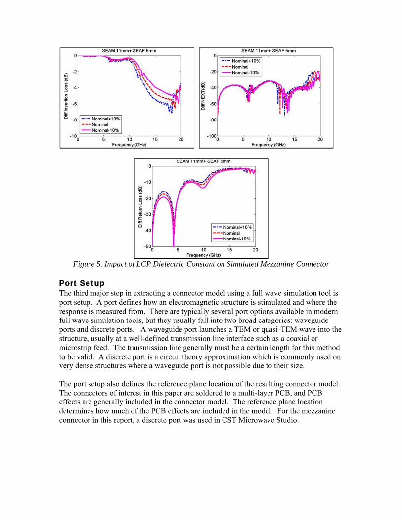
Figure 5. Impact of LCP Dielectric Constant on Simulated Mezzanine Connector
Port Setup The third major step in extracting a connector model using a full wave simulation tool is port setup. A port defines how an electromagnetic structure is stimulated and where the response is measured from. There are typically several port options available in modern full wave simulation tools, but they usually fall into two broad categories: waveguide ports and discrete ports. A waveguide port launches a TEM or quasi-TEM wave into the structure, usually at a well-defined transmission line interface such as a coaxial or microstrip feed. The transmission line generally must be a certain length for this method to be valid. A discrete port is a circuit theory approximation which is commonly used on very dense structures where a waveguide port is not possible due to their size. The port setup also defines the reference plane location of the resulting connector model. The connectors of interest in this paper are soldered to a multi-layer PCB, and PCB effects are generally included in the connector model. The reference plane location determines how much of the PCB effects are included in the model. For the mezzanine connector in this report, a discrete port was used in CST Microwave Studio.

Connector Models from Measurement To establish confidence in a connector model, it is good engineering practice to validate the model. Validation can be done either by comparing the model to one extracted using a different method, either through measurements or by comparison to other modeling tools. While comparison of models extracted using different tools is widely accepted in some industries, the high speed digital community generally prefers model validation through measurements. There are pitfalls in this approach, as measured results can vary widely depending on test fixtures, reference plane location and calibration. The high density connectors that are the subject of this paper do not have coaxial interfaces which mate with modern instrumentation. Rather, a test fixture is required to interface the instrumentation leads to the device. This is typically a multilayer PCB which includes the footprint effects of the connector. Pad capacitance and via stub effects are considered footprint effects. Generally, it is accepted that these footprint effects between the PCB and the connector are included in the connector model. For model correlation, the test fixture either needs to be included in the simulation or removed from the measurement via de-embedding techniques. Due to model complexities, it is preferred to de-embed the test fixture. The de-embedding method will use the Thru-Reflect-Line-Match (TRL/M) method available on modern Vector Network Analyzers (VNA). The accuracy and validity of any VNA measurement is dependent on how much the implicit calibration assumptions are violated. For example, a typical Short-Open-Load-Thru (SOLT) calibration is compromised with poorly constructed calibration standards. If the open calibration standard has fringing capacitance, this must be accounted for in the calibration process as this violates the assumption that the open has a reflection coefficient of unity. This is why instrument manufacturers develop very precise SOLT calibration standards. Fixture removal using TRL/M calibration is no different, in that poorly constructed calibration standards will result in measurement inaccuracies. One assumption of the TRL/M method is that the line standards have the same impedance as the fixture. This seems reasonable until we consider that industry standard impedance control of high density PCBs is +/-10 %. To illustrate the impact of line standard impedance, consider two different sets of on-board TRL/M calibration standards as shown in Figure 6. Notice that the calibration traces in the “66 position” PCB have reasonable, but sharper bends compared to the “44 position” bends. Theses calibration traces were tested for impedance, and it was found the calibration traces with sharper bends (66 position) had more impedance variation than the calibration traces with few bends (44 position). This impedance variation translates into measurement error with TRL/M calibration.

Figure 6. TRL/M Calibration Standards. “66 position” (Left), “44 position” (Right)
Figure 7 shows the variation in measured insertion loss of the same type of connector using two different test fixtures with their associated on-board TRL/M calibration standards. In principle, the two curves in Figure 7 should be identical; instead, we see roughly 0.5 dB variation and some shifting in resonant points.
Figure 7. Measured Insertion Loss of QRate™ QDM8 Series Using Two Different
TRL/M Calibration Kits This example also illustrates a common problem with fixture design in that minor footprint differences can manifest as significant connector measurement variations. Close examination of the artwork reveals minor differences as shown in Figure 8. Notice that the pad trace connecting the ground via to the connector pad is slightly longer in the “66 position” case compared to the “44 position” case. This minor footprint difference resulted in the resonance shift observed in Figure 7 and was verified through full wave modeling of the connector and footprint.

Figure 8. Minor Footprint Differences, “66 position” (Left), “44 position” (Right)
The above example is good case study, but in reality, there are two variables: footprint differences and TRL/M calibration standard variations. The next example has only a minor footprint variation. Figure 9 shows two different footprints: Case 1 and Case 2. Case 1 on the left has the ground vias “outboard” or away from the center of the connector. This method results in more optimal return current flow, but at the expense of a more difficult routing pattern. Case 2 on the right has the ground vias “inboard” or toward the center of the connector. Note that this routing results in a more generous clearance between the signal traces and the ground via.
Figure 9. FT5/FS5 Footprint, Case 1 (left), Case 2 (Right)

Figure 10 shows that there is as much as 10 dB variation in crosstalk at 10 GHz due to this minor variation in ground via orientation.
Figure 10. Impact of Ground Via Orientation on FT5/FS5 Series Measured Connector
Performance
Mechanical Variations There are mechanical variations involved with the test structures (and real world products) including insertion depth and solder variations. Often the SI effects due to these variations are ignored, but to be thorough, they need to be analyzed. The first mechanical variation to consider is connector insertion depth. With any high density, multi-pin connector, there is mechanical tolerance built into the connector to allow for tolerance build up in the mechanical packaging. Figure 11 illustrates the mechanical variation in a mezzanine connector. This product will maintain sufficient normal force at the contact interface with up to 1.15 mm of separation.

Figure 11. Mated Connector Fully Seated (Left) and with 1.15mm Separation (Right)
The connector was simulated when fully mated and with maximum separation using CST Microwave Studio. Care was taken to account for the variation in contact shape between the cases and to include the larger air void when the 2 halves are separated. Results are shown in Figure 12 and show roughly the same level of variation as seen with varying mesh density and changing connector housing dielectric constant.
Figure 12. Simulated Mezzanine Connector Performance When Fully Mated and with
1.15mm of Separation A second mechanical variation, that is assumed to be small, is the variation in board attachment. For a surface mount connector, the connector does not always sit on the

center of the BGA pad on the PCB. Tolerances in PCB registration and assembly variation can cause a degree of wander from true position. Figure 13 illustrates this variation in positioning.
Figure 13.Surface Mount Connector Attachment Variation,
Centered on Pad (Left), Shifted to Edge of Pad (Right)
The results from these simulations on board attachment are shown in Figure 14. In comparison to the changes in mesh density and dielectric constant variation, board attachment has a relatively small effect.
Figure 14. Simulated Performance of Variations in Board Attachment
The main point to take from these examples is that measuring the connector response can be as complex as extracting a connector model from simulation. Care must be taken to be sure that the measured and modeled structures are exactly the same before any attempt at correlation is attempted.

Correlation Correlating measured and simulated connector performance can take several forms. Qualitative terms such as “good” and “reasonable” are common, but can mean very different things depending on the context and background of the people involved. Quantitative terms, such as peak difference in dB, are also problematic. For example, a 10 dB difference in crosstalk when the levels are at -90 dB is very different than if the levels are at -20 dB. Also, is comparing the magnitude sufficient or should magnitude and phase be considered? Later in this paper, two different quantitative methods of comparing data sets will be applied to the next example. To begin the correlation discussion, consider the measured and simulated performance of a 16 mm high density mezzanine connector. The simulated response was generated using a full wave modeling tool. Care was taken to ensure that sufficient mesh density and port setup protocols were followed using nominal dielectric material characteristics. The measured response includes the connector and footprint. On-board TRL/M calibration structures were used to calibrate the VNA and de-embed the test fixture effects. Care was taken to ensure the footprint measured exactly matches the simulated footprint. The results are shown in Figure 15. In comparing the responses in Figure 15, the correlation is generally within expectations. The impedance profile shown in Figure 15 was generated from the measured/simulated touchstone files using time domain convolution.
Figure 15. Measured and Simulated Performance of 16mm Mezzanine Connector

Intel has publicly released a document concerning connector model quality in September 2011 [2]. This document introduces the concept of Model Quality Factor (MQF) as a means of gauging the accuracy of a simulation based model compared to measured performance where:
2
110log
x
xxx
xx= Model Quality Factor for impedance, insertion loss and crosstalk x1= reference area x2= area between measured and simulated curves
An MQF with a large positive value indicates a high degree of correlation. An MQF with a small (or negative) value indicates relatively poor correlation. The method relies upon computing areas on time domain graphs. This method was applied to the results shown in Figure 15 for a 16 mm mezzanine connector. The first step in computing MQF is to transform the S-Parameter connector model and measurements into Time Domain graphs. This was done using Agilent ADS 2011.05. The MQF for impedance was calculated to be -0.15 indicating relatively poor correlation. This is due to the simulated impedance being low in comparison to the measured value. Figure 16 illustrates the area calculation in the MQF computation. Note that the span of the MQF is limited to the connector region or twice the propagation time of the connector on a graph of impedance versus time. Impedance MQF does not specify rise time; however, rise time does affect MQF. Figure 16 had a source rise time of 30 ps (20-80%) which resulted in a MQF of -0.15. At a rise time of 50 ps, the MQF degraded to -0.28, and at 100 ps, the MQF dropped to -0.6.
Figure 16. Impedance MQF Area Calculation, Reference (Left), Area Between Curves (Right)

The insertion loss MQF is based on the Time Domain Transmission (TDT) response. Rise Time Degradation, or TDT, is equivalent to insertion loss provided the source rise time is defined. The MQF for insertion loss was calculated to be 0.43, and the corresponding analysis is shown in Figure 17.
Figure 17. Insertion Loss MQF Area Calculation,
Reference (Left), Area Between Curves (Right) The near end crosstalk (NEXT) MQF is likewise based on the Time Domain Transmission (TDT) response. Time Domain NEXT is also dependent on the source rise time which is not specified. The MQF for NEXT was calculated to be 0.85, and the corresponding analysis is shown in Figure 18.
Figure 18. NEXT MQF Area Calculation,
Reference (Left), Area Between Curves (Right) An alternate method of correlating two data sets is Feature Selective Validation (FSV) [3-6]. FSV has an advantage over MQF in that it can be applied to Time or Frequency Domain data sets. MQF has an advantage in that it is much simpler to implement if writing original code. FSV results in a qualitative value ranging from excellent to poor. These map to FSV quantitative values of < 0.1 (excellent) to >1.6 (poor). FSV considers the absolute difference between two data sets and terms this the Amplitude Difference Measure

(ADM). For example, achieving good correlation across a wide spectrum with a fairly constant dependent variable would show up as a low ADM. FSV also considers the feature differences in two data sets calculated as the 1st derivative of the data to accentuate changes in the curves. This is referred to as the Feature Difference Measure (FDM). For example, good correlation of a connector resonance would show up as a low value of FDM. The geometric mean of the ADM and FDM combine to form the Global Difference Measure (GDM). GDM can be considered the overall correlation between two data sets. ADM, FDM and GDM can be plotted over the independent variable span to show where the models are similar or different. It is also common to plot the histogram to show what percentages of data points have good correlation. The histogram is broken into six categories, with quantitative terms mapped to the qualitative histogram categories. The FSV application is available for download at www.upd.edu/web/gcem [6] and was used to create Figures 19-21. Figure 19 shows that the measured and simulated insertion loss data sets which had “very good” correlation based on the GDMtot value of 0.13. GDMtot is essentially a “one number rating” that includes amplitude and feature differences in the data sets.
Figure 19. ADM, FDM and GDM Histograms for the 16mmm Mezzanine Connector
(Insertion Loss) Figure 20 shows that the measured and simulated NEXT data sets had “good” correlation based on the GDMtot value of 0.3. As with the insertion loss data, both ADM and FDM showed better correlation than the geometric mean.

Figure 20. ADM, FDM and GDM Histograms for the 16mmm Mezzanine Connector
(NEXT) Figure 21 shows that the measured and simulated impedance data sets had “fair” correlation based on the GDMtot value of 0.75.
Figure 21. ADM, FDM and GDM Histograms for the 16mmm Mezzanine Connector
(Return Loss)

Conclusions and Recommendations Validation of multi-pin, high speed connectors has been shown to be a challenge as the influence of an imperfect test fixtures complicates matters. On the measurement side, accurate on-board calibration standards are required for consistent de-embedding. On the simulation side, connector material parameters are estimations, and model mesh density can impact the results. It is critical that the measured footprint be included in the simulation as minor footprint differences will result in variations between measured and simulated results. Two different model quality metrics were applied to the measured and simulated connector differential S-Parameters. These metrics are demanding for these model types, and achieving very good correlation is challenging given the complexity of the microwave structures. The transmission parameters (IL and NEXT) tended to show better correlation compared to the reflection parameters (RL and impedance). The qualitative rating of FSV is a major advantage compared to MQF; however FSV has undergone many years of iteration to reach its mature state. So, are connector models any good? For this example, yes they are according the FSV.
Acknowledgments The authors would like to thank our dedicated lab personnel of Henry Dai, Viky Jia and Craig Rapp for their many hours of effort in support of this paper. The guidance and insight of Scott McMorrow and Al Neves on connector modeling and testing has been instrumental in achieving a reasonable level of correlation.

References [1] Tektronix IConnect and MeasureXtractor User Manual [2] Intel Corporation, “Intel Connector Model, Quality Assessment Methodology”,
September 2011 [3] Roy Leventhal, “Correlation of Model Simulations and Measurements” IBIS Summit
Meeting, June 5, 2007 [4] IEEE P1597.2/D6.4 “Draft Recommended Practice for Validation of Computational
Electromagnetic Computer Modeling and Simulation” [5] J. Knockaert, J. Cartrysse, R. Belmans “Comparison and Validation of EMC
Measurementsby FSV and IELF”, 2006 IEEE [6] Universitat Politecnica De Catalunya, FSV downloadable code