sata i/ii/iii bidirectional redriver with input equalization - maxim
TRANSCRIPT

_______________________________________________________________ Maxim Integrated Products 1
For pricing, delivery, and ordering information, please contact Maxim Direct at 1-888-629-4642, or visit Maxim’s website at www.maxim-ic.com.
SATA I/II/III Bidirectional Redriver with Input Equalization and Preemphasis M
AX
49
51
BE
19-5023; Rev 1; 11/10
General DescriptionThe MAX4951BE dual-channel buffer is ideal to redrive serial ATA (SATA) I, SATA II, and SATA III signals and features high electrostatic discharge (ESD) Q8kV Human Body Model (HBM) protection. The MAX4951BE can be placed nearly anywhere on the motherboard to over-come board losses and produce an eSATA-compatible signal level. This device is SATA specification v.2.6 (gold standard)-compliant, while overcom ing losses in the PCB and eSATA connector.
The MAX4951BE features very low standby current for power-sensitive applications. This device features hard-ware SATA-drive cable detection, keeping the power low in standby mode. The device also features an indepen-dent channel, dynamic power-down mode where power consumption is reduced when no input signal is present.
The MAX4951BE preserves signal integrity at the receiv-er by reestablishing full output levels and can reduce the total system jitter (TJ) by providing input equaliza-tion. This device features channel-independent digital preemphasis controls to drive SATA outputs over longer trace lengths or to meet eSATA specifications. SATA Out-Of-Band (OOB) signaling is supported using high-speed OOB signal detection on the inputs and squelch on the corresponding outputs. Inputs and outputs are all internally 50I terminated and must be AC-coupled to the SATA controller IC and SATA device.
The MAX4951BE operates from a single +3.3V (typ) supply, and is available in a small, 4mm x 4mm TQFN package with flow-through traces for ease of layout. This device is specified over the 0NC to +70NC operating temperature range.
ApplicationsLaptop Computers
Servers
Desktop Computers
Docking Stations
Data Storage/Workstations
FeaturesS Single +3.3V Supply Operation
S Low-Power, 500µA (typ) eSATA Cable Detect
S Drive Detection
S Dynamic Power Reduction Reduced Power Consumption in Active Mode
S Fixed Input Equalization Permits Longer Traces Leading to the Device
S Selectable Output Preemphasis Improved Output Eye
S SATA I (1.5Gbps) and SATA II (3.0Gbps) Compliant
S SATA III (6.0Gbps) Compliant
S Supports eSATA Output Levels
S Supports SATA OOB Signaling
S OOB Detection: 8ns (max)
S Internal Input/Output 50I Termination Resistors
S Inline Signal Traces for Flow-Through Layout
S Space-Saving, 4mm x 4mm TQFN Package with Exposed Pad
S High ESD Protection on All Pins: ±8kV (HBM)
Ordering Information
+Denotes a lead(Pb)-free/RoHS-compliant package.*EP = Exposed pad.
EVALUATION KIT
AVAILABLE
PART TEMP RANGE PIN-PACKAGE
MAX4951BECTP+ 0NC to +70NC 20 TQFN-EP*

SATA I/II/III Bidirectional Redriver with Input Equalization and Preemphasis
MA
X4
95
1B
E
2 ______________________________________________________________________________________
Stresses beyond those listed under “Absolute Maximum Ratings” may cause permanent damage to the device. These are stress ratings only, and functional operation of the device at these or any other conditions beyond those indicated in the operational sections of the specifications is not implied. Exposure to absolute maximum rating conditions for extended periods may affect device reliability.
(All voltages referenced to GND unless otherwise noted.)VCC .......................................................................-0.3V to +4.0VAINP, AINM, BINP, BINM, EN, CAD, PA, PB (Note 1) .......................................-0.3V to (VCC +0.4V)Short-Circuit Output Current (BOUTP, BOUTM, AOUTP, AOUTM) ...........................Q30mAContinuous Current at Inputs (AINP, AINM, BINP, BINM) ............................................Q5mA
Continuous Power Dissipation (TA = +70NC) TQFN (derate 25.6mW/NC above +70NC) ..................2051mWESD Protection on All Pins (HBM) .......................................Q8kVOperating Temperature Range ............................. 0NC to +70NCStorage Temperature Range ............................ -55NC to +150NCLead Temperature (soldering, 10s) ................................+300NCSoldering Temperature (reflow) ......................................+260NC
ELECTRICAL CHARACTERISTICS(VCC = +3.0V to +3.6V, CL = 12nF, RL = 50I, TA = 0NC to +70NC, unless otherwise noted. Typical values are at VCC = +3.3V, TA = +25NC.) (Note 3)
ABSOLUTE MAXIMUM RATINGS
Note 2: Package thermal resistances were obtained using the method described in JEDEC specification JESD51-7, using a four-layer board. For detailed information on package thermal considerations, refer to www.maxim-ic.com/thermal-tutorial.
PACKAGE THERMAL CHARACTERISTICS (Note 2)TQFN Junction-to-Ambient Thermal Resistance (qJA) ...........39°C/W Junction-to-Case Thermal Resistance (qJC) ..................6°C/W
Note 1: All I/O pins are clamped by internal diodes.
PARAMETER SYMBOL CONDITIONS MIN TYP MAX UNITS
Operating Power-Supply Range VCC 3.0 3.6 V
Operating Supply Current ICC
PA = PB = VCC;D10.2 pattern, f = 1.5Gbps
77 92
mAPA = PB = GND;D10.2 pattern, f = 1.5Gbps
62 76
Average Supply Current in Normal Operation
Duty cycle is 25% active, 75% idle; D10.2 pattern
Preemphasis on 30mA
Preemphasis off 26
Standby Supply Current ISTBY EN = GND or CAD = VCC 500 750 FA
Dynamic Power-Down Current IDYNPD 14 20 mA
Single-Ended Input Resistance ZRX-SE-DC Single-ended to VCC (Note 4) 40 50 I
Differential Input ResistanceZRX-DIFF-
DC(Note 4) 85 100 115 I
Single-Ended Output Resistance ZTX-SE-DC Single-ended to VCC (Note 4) 40 50 I
Differential Output Resistance ZTX-DIFF-DC (Note 4) 85 100 115 I
AC PERFORMANCE
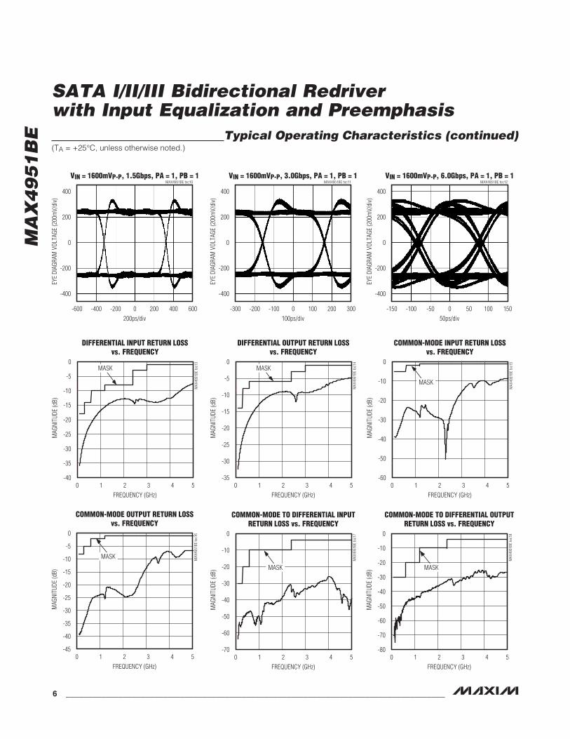
Differential Input Return Loss(Notes 4, 5)
RLRX-DIFF
f = 150MHz to 300MHz 18
dB
f = 300MHz to 600MHz 14
f = 600MHz to 1200MHz 10
f = 1.2GHz to 2.4GHz 8
f = 2.4GHz to 3.0GHz 3
f = 3.0GHz to 5.0GHz 1

SATA I/II/III Bidirectional Redriver with Input Equalization and Preemphasis
MA
X4
95
1B
E
_______________________________________________________________________________________ 3
ELECTRICAL CHARACTERISTICS (continued)(VCC = +3.0V to +3.6V, CL = 12nF, RL = 50I, TA = 0NC to +70NC, unless otherwise noted. Typical values are at VCC = +3.3V, TA = +25NC.) (Note 3)
PARAMETER SYMBOL CONDITIONS MIN TYP MAX UNITS
Common-Mode Input Return Loss (Notes 4, 5)
RLRX-CM
f = 150MHz to 300MHz 5
dB
f = 300MHz to 600MHz 5
f = 600MHz to 1200MHz 2
f = 1.2GHz to 2.4GHz 1
f = 2.4GHz to 3.0GHz 1
f = 3.0GHz to 5.0GHz 1
Differential Output Return Loss(Notes 4, 5)
RLTX-DIFF
f = 150MHz to 300MHz 14
dB
f = 300MHz to 600MHz 8
f = 600MHz to 1200MHz 6
f = 1.2GHz to 2.4GHz 6
f = 2.4GHz to 3.0GHz 3
f = 3.0GHz to 5.0GHz 1
Common-Mode Output Return Loss (Notes 4, 5)
RLTX-CM
f = 150MHz to 300MHz 8
dB
f = 300MHz to 600MHz 5
f = 600MHz to 1200MHz 2
f = 1.2GHz to 2.4GHz 1
f = 2.4GHz to 3.0GHz 1
f = 3.0GHz to 5.0GHz 1
Common-Mode to Differential Input Return Loss (Notes 4, 5)
RLRX-CM-DM
f = 150MHz to 300MHz 30
dB
f = 300MHz to 600MHz 20
f = 600MHz to 1200MHz 10
f = 1.2GHz to 2.4GHz 10
f = 2.4GHz to 3.0GHz 4
f = 3.0GHz to 5.0GHz 4
Common-Mode to Differential Output Return Loss (Notes 4, 5)
RLTX-CM-DM
f = 150MHz to 300MHz 30
dB
f = 300MHz to 600MHz 30
f = 600MHz to 1200MHz 20
f = 1.2GHz to 2.4GHz 10
f = 2.4GHz to 3.0GHz 4
f = 3.0GHz to 5.0GHz 4
Differential Input Signal Range VRX-DFF-PP SATA I, SATA II (Note 4) 225 1600 mVP-P
Differential Output Swing VTX-DFF-PP f = 750MHz (Note 4) PA = PB = GND 425 525 625 mVP-P
Output PreemphasisTX-DFF-PP-
PEDBf = 750MHz PA = PB = VCC 2.8 dB
Input EqualizationVRX-DFF-PP = 300mVP-P,tIN,RISE/FALL = 20ps
2.7 dB
Preemphasis Time Period tPE f = 750MHz PA = PB = VCC 150 ps
Propagation Delay tPD 150 ps

SATA I/II/III Bidirectional Redriver with Input Equalization and Preemphasis
MA
X4
95
1B
E
4 ______________________________________________________________________________________
ELECTRICAL CHARACTERISTICS (continued)(VCC = +3.0V to +3.6V, CL = 12nF, RL = 50I, TA = 0NC to +70NC, unless otherwise noted. Typical values are at VCC = +3.3V, TA = +25NC.) (Note 3)
Note 3: All devices are 100% production tested at TA = +70°C. All temperature limits are guaranteed by design.Note 4: This specification meets SATA v.2.6, gold standard.Note 5: Guaranteed by design.Note 6: Rise and fall times are measured using 20% and 80% levels.Note 7: For SATA 2.0, refer to SATA 2.6-Gold Specification, page 111, Figure 191.Note 8: For SATA 3.0, refer to SATA Revision 3.0 Release Candidate, page 222, Figure 124.Note 9: DJ measured using a K28.5 pattern; RJ measured using a D10.2 pattern.Note 10: Total time for OOB detection circuit to enable/squelch the output.
PARAMETER SYMBOL CONDITIONS MIN TYP MAX UNITS
Output Rise/Fall Time(Notes 5, 6)
tR, tF
PA = PB = GNDSATA I/II (Note 7)
67 130
psPA = PB = GNDSATA III (Note 8)
40 68
Deterministic Jitter (Notes 5, 9) tTX-DJ-DD PA = PB = GND 20 psP-P
Random Jitter (Notes 5, 9) tTX-RJ-DD PA = PB = GND 1.5 psRMS
OOB Detector Threshold SATA OOB pattern, f = 750MHz 50 150 mVP-P
OOB Output Startup/Shutdown Time
(Note 10) 4 8 ns
OOB Differential-Offset Delta rVOOB,DFFDifference between OOB and active-mode output offset
-120 120 mV
OOB Common-Mode Delta rVOOB,CMDifference between OOB and active com-mon-mode voltage
-15 +15 mV
OOB Output Disable VOOB,OUT VIN < 50mVP-P, output voltage in squelch 30 mVP-P
LOGIC INPUT
Input Logic-High VIH 1.4 V
Input Logic-Low VIL 0.6 V
Input Logic Hysteresis VHYST 0.1 V
Input Pullup Resistance RPU Pin: CAD 200 330 kI
Input Pulldown Resistance RPD Pins: EN, PA, PB 200 330 kI
ESD PROTECTION
All Pins HBM Q8 kV

SATA I/II/III Bidirectional Redriver with Input Equalization and Preemphasis
MA
X4
95
1B
E
_______________________________________________________________________________________ 5
Typical Operating Characteristics(TA = +25°C, unless otherwise noted.)
VIN = 220mVP-P, 6.0Gbps, PA = 1, PB = 1
50ps/div
EYE
DIAG
RAM
VOL
TAGE
(200
mV/
div)
100500-50-100
-400
-200
0
200
400
-150 150
MAX4951BE toc09VIN = 220mVP-P, 3.0Gbps, PA = 1, PB = 1
100ps/div
EYE
DIAG
RAM
VOL
TAGE
(200
mV/
div)
2001000-100-200
-400
-200
0
200
400
-300 300
MAX4951BE toc08VIN = 220mVP-P, 1.5Gbps, PA = 1, PB = 1
200ps/div
EYE
DIAG
RAM
VOL
TAGE
(200
mV/
div)
4002000-200-400
-400
-200
0
200
400
-600 600
MAX4951BE toc07
VIN = 1600mVP-P, 6.0Gbps, PA = 0, PB = 0
50ps/div
EYE
DIAG
RAM
VOL
TAGE
(200
mV/
div)
100500-50-100
-200
0
200
-150 150
MAX4951BE toc06VIN = 1600mVP-P, 3.0Gbps, PA = 0, PB = 0
100ps/div
EYE
DIAG
RAM
VOL
TAGE
(200
mV/
div)
2001000-100-200
-200
0
200
-300 300
MAX4951BE toc05VIN = 1600mVP-P, 1.5Gbps, PA = 0, PB = 0
200ps/div
EYE
DIAG
RAM
VOL
TAGE
(200
mV/
div)
4002000-200-400
-200
0
200
-600 600
MAX4951BE toc04
VIN = 220mVP-P, 6.0Gbps, PA = 0, PB = 0
50ps/div
EYE
DIAG
RAM
VOL
TAGE
(200
mV/
div)
100500-50-100
-200
0
200
-150 150
MAX4951BE toc03VIN = 220mVP-P, 3.0Gbps, PA = 0, PB = 0
100ps/div
EYE
DIAG
RAM
VOL
TAGE
(200
mV/
div)
2001000-100-200
-200
0
200
-300 300
MAX4951BE toc02VIN = 220mVP-P, 1.5Gbps, PA = 0, PB = 0
200ps/div
EYE
DIAG
RAM
VOL
TAGE
(200
mV/
div)
4002000-200-400
-200
0
200
-600 600
MAX4951BE toc01
SATA I/II/III Bidirectional Redriver with Input Equalization and Preemphasis
MA
X4
95
1B
E
6 ______________________________________________________________________________________
Typical Operating Characteristics (continued)(TA = +25°C, unless otherwise noted.)
COMMON-MODE TO DIFFERENTIAL OUTPUTRETURN LOSS vs. FREQUENCY
MAX
4951
BE to
c18
FREQUENCY (GHz)
MAG
NITU
DE (d
B)
431 2
-60
-70
-50
-40
-30
-20
-10
0
-800 5
MASK
COMMON-MODE TO DIFFERENTIAL INPUTRETURN LOSS vs. FREQUENCY
MAX
4951
BE to
c17
FREQUENCY (GHz)
MAG
NITU
DE (d
B)
431 2
-60
-50
-40
-30
-20
-10
0
-700 5
MASK
COMMON-MODE OUTPUT RETURN LOSSvs. FREQUENCY
MAX
4951
BE to
c16
FREQUENCY (GHz)
MAG
NITU
DE (d
B)
431 2
-35
-40
-30
-25
-20
-15
-10
-5
0
-450 5
MASK
COMMON-MODE INPUT RETURN LOSSvs. FREQUENCY
MAX
4951
BE to
c15
FREQUENCY (GHz)
MAG
NITU
DE (d
B)
431 2
-50
-40
-30
-20
-10
0
-600 5
MASK
DIFFERENTIAL OUTPUT RETURN LOSSvs. FREQUENCY
MAX
4951
BE to
c14
FREQUENCY (GHz)
MAG
NITU
DE (d
B)
431 2
-30
-25
-20
-15
-10
-5
0
-350 5
MASK
DIFFERENTIAL INPUT RETURN LOSSvs. FREQUENCY
MAX
4951
BE to
c13
FREQUENCY (GHz)
MAG
NITU
DE (d
B)
431 2
-35
-30
-25
-20
-10
-15
-5
0
-400 5
MASK
VIN = 1600mVP-P, 6.0Gbps, PA = 1, PB = 1
50ps/div
EYE
DIAG
RAM
VOL
TAGE
(200
mV/
div)
100500-50-100
-400
-200
0
200
400
-150 150
MAX4951BE toc12VIN = 1600mVP-P, 3.0Gbps, PA = 1, PB = 1
100ps/div
EYE
DIAG
RAM
VOL
TAGE
(200
mV/
div)
2001000-100-200
-400
-200
0
200
400
-300 300
MAX4951BE toc11VIN = 1600mVP-P, 1.5Gbps, PA = 1, PB = 1
200ps/div
EYE
DIAG
RAM
VOL
TAGE
(200
mV/
div)
4002000-200-400
-400
-200
0
200
400
-600 600
MAX4951BE toc10

SATA I/II/III Bidirectional Redriver with Input Equalization and Preemphasis
MA
X4
95
1B
E
_______________________________________________________________________________________ 7
Typical Operating Characteristics (continued)(TA = +25°C, unless otherwise noted.)
EYE HEIGHT vs. OUTPUT LENGTH,PA = 1, PB = 1 (7.5in OF INPUT TRACE)
MAX
4951
BE to
c24
LENGTH (in)
EYE
HEIG
HT (m
V)
252015105
50
100
150
200
250
300
350
400
450
500
00 30
VIN = 1VP-P
6Gbps,NONTRANSITION BITS
3Gbps,NONTRANSITION BITS
6Gbps,TRANSITION BITS
3Gbps,TRANSITION BITS
DETERMINISTIC JITTER vs. OUTPUT LENGTH,PA = 1, PB = 1
MAX
4951
BE to
c23
LENGTH (in)
DETE
RMIN
ISTI
C JI
TTER
(ps P
-P)
252015105
5
10
15
20
25
30
35
40
45
00 30
VIN = 1VP-P, 7.5in OF INPUT TRACE
3Gbps
6Gbps
EYE HEIGHT vs. OUTPUT LENGTH,PA = 0, PB = 0 (7.5in OF INPUT TRACE)
MAX
4951
BE to
c22
LENGTH (in)
EYE
HEIG
HT (m
V)
252015105
50
100
150
200
250
300
350
400
450
500
00 30
VIN = 1VP-P
6Gbps, TRANSITION BITS
6Gbps,NONTRANSITION BITS
3Gbps,NONTRANSITION BITS
3Gbps,TRANSITION BITS
DETERMINISTIC JITTER vs. OUTPUT LENGTH,PA = 0, PB = 0
MAX
4951
BE to
c21
LENGTH (in)
DETE
RMIN
ISTI
C JI
TTER
(ps P
-P)
252015105
20
40
60
80
100
120
140
00 30
3Gbps
6Gbps
VIN = 1VP-P, 7.5in OF INPUT TRACE
EYE HEIGHT vs. INPUT LENGTH,PA = 0, PB = 0
MAX
4951
BE to
c20
LENGTH (in)
EYE
HEIG
HT (m
V)
5040302010
100
200
300
400
500
600
00 60
VIN = 1VP-P 3Gbps, NONTRANSITION BITS
6Gbps,NONTRANSITION BITS
6Gbps,TRANSITION BITS 3Gbps,
TRANSITION BITS
DETERMINISTIC JITTER vs. INPUT LENGTH,PA = 0, PB = 0
MAX
4951
BE to
c19
LENGTH (in)
DETE
RMIN
ISTI
C JI
TTER
(ps P
-P)
5040302010
50
100
150
200
250
300
00 60
VIN = 1VP-P
3Gbps
6Gbps

SATA I/II/III Bidirectional Redriver with Input Equalization and Preemphasis
MA
X4
95
1B
E
8 ______________________________________________________________________________________
Pin Configuration
Pin Description
19
20
18
17
7
6
8
AINM
BOUT
P
9
AINP
AOUT
M
BINM
BINP
AOUT
P
1 2
CAD
4 5
15 14 12 11
GND
VCC
PA
PB
EN
+ VCCGN
DGN
D
3
13
GND
16 10 VCCVCC
TQFN(4mm × 4mm)
TOP VIEW
BOUT
M
*EP
*CONNECT EXPOSED PAD (EP) TO GND.
MAX4951BE
PIN NAME FUNCTION
1 AINP Noninverting Input from Host Channel A
2 AINM Inverting Input from Host Channel A
3, 13, 17, 19 GND Ground
4 BOUTM Inverting Output to Host Channel B
5 BOUTP Noninverting Output to Host Channel B
6, 10, 16, 20 VCCPositive Supply Voltage Input. Bypass VCC to GND with 1FF and 0.01FF capacitors in parallel as close to the device as possible.
7 ENActive-High Enable Input. Drive EN low to put the device in standby mode. Drive EN high for nor-mal operation. EN is internally pulled down with a 330kW (typ) resistor.
8 PBChannel B Preemphasis Enable Input. Drive PB high to enable channel B output preemphasis. Drive PB low for standard SATA output level. PB is internally pulled down with a 330kW (typ) resistor.
9 PAChannel A Preemphasis Enable Input. Drive PA high to enable channel A output preemphasis. Drive PA low for standard SATA output level. PA is internally pulled down with a 330kW (typ) resistor.
11 BINP Noninverting Input from Device Channel B
12 BINM Inverting Input from Device Channel B
14 AOUTM Inverting Output to Device Channel A
15 AOUTP Noninverting Output to Device Channel A
18 CADActive-Low Cable-Detect Input. Drive CAD high to put the device in standby mode. Drive CAD low for normal operation. CAD is internally pulled up with a 330kI (typ) resistor.
— EPExposed Pad. Internally connected to GND. EP must be electrically connected to a ground plane for proper thermal and electrical operation.

SATA I/II/III Bidirectional Redriver with Input Equalization and Preemphasis
MA
X4
95
1B
E
_______________________________________________________________________________________ 9
Detailed DescriptionThe MAX4951BE consists of two identical buffers that take SATA input signals and return them to full output levels while withstanding high ESD Q8kV (HBM) protec-tion. This device meets SATA I/II specifications and can meet SATA III specifications.
Input/Output TerminationsInputs and outputs are internally 50I terminated to VCC (see the Functional Diagram/Truth Table) and must be AC-coupled to the SATA controller IC and SATA device for proper operation.
Functional Diagram/Truth Table
Note: PA, PB, EN are internally pulled down to GND by 330kW resistors. CAD is internally pulled up to VCC by a 330kW resistor.
X = Don’t care.
VCC
VCC
50Ω50Ω
VCC
50Ω50Ω
VCC
50Ω50Ω
VCC
50Ω50Ω
CONTROL LOGIC
AOUTPAINP
AOUTMAINM
BINMBOUTM
BINPBOUTP
PB EN CADPA
GND
MAX4951BE
EN CAD STATUS
0 0 Low-Power Standby
0 1 Low-Power Standby
1 0 Active
1 1 Low-Power Standby
EN PA PB CHANNEL A CHANNEL B
0 X X Standby Standby
1 0 0 Standard SATA Standard SATA
1 1 0 Preemphasis Standard SATA
1 0 1 Standard SATA Preemphasis
1 1 1 Preemphasis Preemphasis

SATA I/II/III Bidirectional Redriver with Input Equalization and Preemphasis
MA
X4
95
1B
E
10 _____________________________________________________________________________________
OOB Signal DetectionThe MAX4951BE provides full OOB signal support through high-speed, OOB-detection circuitry. SATA OOB differential input signals of 50mVP-P or less are detected as OFF and are not passed to the output. This prevents the system from responding to unwanted noise. SATA OOB differential input signals of 150mVP-P or more are detected as on and passed to the output. This allows OOB signals to transmit through the MAX4951BE. The time for the OOB-detection circuit to detect an inactive SATA OOB input and squelch the associated output, or to detect an active SATA OOB input and enable the output, is less than 4ns (typ).
Enable InputThe MAX4951BE features an active-high enable input (EN). EN has an internal pulldown resistor of 330kI (typ). When EN is driven low or left unconnected, the MAX4951BE enters low-power standby mode and the buffers are disabled, reducing the supply current to 500FA (typ). Drive EN high for normal operation.
Cable-Detect InputThe MAX4951BE features an active-low, cable-detect input (CAD). CAD has an internal pullup resistor of 330kI (typ). When CAD is driven high or left uncon-nected, the MAX4951BE enters low-power standby mode and the buffers are disabled, reducing supply current to 500FA (typ). This signal is normally driven low by inserting an eSATA cable into a properly wired socket (see Figure 3). If the cable-detect feature is not desired, simply ground this pin.
Dynamic Power-Down ModeThe MAX4951BE features a dynamic power-down mode where the device shuts down the major power consump-
tion circuitry. The MAX4951BE detects whether the input signal does not exist for a 4Fs (typ) duration. Normal power and normal operation resume when a signal above the OOB-threshold level is detected at the input. This function is implemented separately for both chan-nels.
Output Preemphasis Selection InputsThe MAX4951BE has two preemphasis-control logic inputs, PA and PB. PA and PB have internal pulldown resistors of 330kI (typ). PA and PB enable preemphasis to the outputs of their corresponding buffers (see the Functional Diagram/Truth Table). Drive PA or PB low or leave unconnected for standard SATA output levels. Drive PA or PB high to provide preemphasis to the out-put. The preemphasis output signal compensates for attenuation from longer trace lengths or to meet eSATA specifications.
ESD ProtectionAs with all Maxim devices, ESD protection structures are incorporated on all pins to protect against electrostatic discharges encountered during handling and assembly. The MAX4951BE is protected against ESD Q8kV (HBM). The ESD struc tures withstand Q8kV in normal opera-tion and powered down states. After an ESD event, the MAX4951BE continues to function without latchup.
HBMThe MAX4951BE is characterized for Q8kV ESD pro-tection using the HBM (MIL-STD-883, Method 3015). Figure 1 shows the HBM and Figure 2 shows the cur-rent waveform it generates when discharged into a low-impedance state. This model con sists of a 100pF capacitor charged to the ESD voltage of interest that is then discharged into the device through a 1.5kI resistor.
Figure 1. Human Body ESD Test Model Figure 2. Human Body Current Waveform
CHARGE-CURRENTLIMIT RESISTOR
DISCHARGERESISTANCE
STORAGECAPACITOR
CS100pF
RC1MΩ
RD 1500Ω
HIGH-VOLTAGE
DCSOURCE
DEVICEUNDERTEST
IP 100%90%
36.8%
tRLTIME
tDLCURRENT WAVEFORM
PEAK-TO-PEAK RINGING(NOT DRAWN TO SCALE)
Ir
10%0
0
AMPS

SATA I/II/III Bidirectional Redriver with Input Equalization and Preemphasis
MA
X4
95
1B
E
______________________________________________________________________________________ 11
Applications InformationFigure 3 shows a typical application with the MAX4951BE used to drive an eSATA output. The diagram assumes that the MAX4951BE is close to the SATA host controller. PB is set low to drive standard SATA levels to the host, and PA is set high to drive eSATA levels to the device. If the MAX4951BE is further from the controller, set PB high to compensate for attenuation. The MAX4951BE is backward-pin-compatible with MAX4951 (see Figure 4).
Exposed-Pad PackageThe exposed-pad, 20-pin TQFN package incorporates features that provide a very low thermal resistance path for heat removal from the IC. The exposed pad on the MAX4951BE must be soldered to GND for proper ther-mal and electrical performance. For more information on
exposed-pad packages, refer to Application Note 862: HFAN-08.1: Thermal Considerations of QFN and Other Exposed-Paddle Packages.
LayoutUse controlled-impedance transmission lines to interface with the MAX4951BE high-speed inputs and outputs. Place power-supply decoupling capacitors as close as possible to VCC pin.
Power-Supply SequencingCaution: Do not exceed the absolute maximum rat-ings because stresses beyond the listed ratings can cause permanent damage to the device.
Proper power-supply sequencing is recommended for all devices. Always apply VCC before applying signals, especially if the signal is not current limited.
Figure 3. Typical Application Circuit for MAX4951BE Driving an eSATA Output
EN
GPIO
+3.3V
0.01µF1µF
GNDPB
VCC
PA
VCC
SATA HOSTCONTROLLER
eSATADEVICE
CONNECTOR
Rx
1
4
5
6
7 OR 1*
*PINS 1 AND 7 CAN BE INTERCHANGED DEPENDING ON THE LAYOUT.
2
3
Tx
10nF (X7R)
10nF (X7R)
10nF (X7R)
10nF (X7R)
10nF (X7R)
10nF (X7R)
10nF (X7R)
10nF (X7R)
AINP
AINM
BOUTM
BOUTP
AOUTP
AOUTM
BINM
BINP
CAD
Tx
Rx
MAX4951BE

SATA I/II/III Bidirectional Redriver with Input Equalization and Preemphasis
MA
X4
95
1B
E
12 _____________________________________________________________________________________
Chip InformationPROCESS: BiCMOS
Package InformationFor the latest package outline information and land patterns, go to www.maxim-ic.com/packages. Note that a “+”, “#”, or “-” in the package code indicates RoHS status only. Package drawings may show a different suffix character, but the drawing pertains to the package regardless of RoHS status.
Figure 4. Typical Application Circuit for Backward Pin Compatibility with the MAX4951
+3.3V
0.01µF
*PINS 1 AND 7 CAN BE INTERCHANGED DEPENDING ON THE LAYOUT.
1µF
VCC
SATA HOSTCONTROLLER
eSATADEVICE
CONNECTOR
Rx
1
4
5
6
7 OR 1*
2
3
Tx
10nF (X7R)
10nF (X7R)
10nF (X7R)
10nF (X7R)
10nF (X7R)
10nF (X7R)
10nF (X7R)
10nF (X7R)
AINP
AINM
BOUTM
BOUTP
AOUTP
AOUTM
BINM
BINP
Tx
Rx
MAX4951BE
EN
GPIO
GNDPBPA
VCC
CAD
PACKAGE TYPE
PACKAGE CODE
OUTLINE NO.
LANDPATTERN NO.
20 TQFN-EP T2044+2 21-0139 90-0036

SATA I/II/III Bidirectional Redriver with Input Equalization and Preemphasis
MA
X4
95
1B
E
Maxim cannot assume responsibility for use of any circuitry other than circuitry entirely embodied in a Maxim product. No circuit patent licenses are implied. Maxim reserves the right to change the circuitry and specifications without notice at any time.
Maxim Integrated Products, 120 San Gabriel Drive, Sunnyvale, CA 94086 408-737-7600 13
© 2010 Maxim Integrated Products Maxim is a registered trademark of Maxim Integrated Products, Inc.
Revision History
REVISION NUMBER
REVISION DATE
DESCRIPTIONPAGES
CHANGED
0 10/09 Initial release —
1 11/10Deleted the “Meets SATA I, II Input/Output-Return Loss Mask” feature from the Features section, deleted the “Top Mark” column from the Ordering Information
1