scalable and reusable micro-bubble removal method to...
TRANSCRIPT

1
Scalable and Reusable Micro-Bubble Removal Method to Flatten Large-Area 1 2D Materials 2
3 Phi H.Q. Pham†, Nhi V. Quach†, Jinfeng Li†, Peter J. Burke† 4
5 †Department of Electrical Engineering and Computer Science, University of California, Irvine, 6
California 92697, United States 7
Abstract: 8 Bubbles generated during electro-delamination and chemical etch during large-area two-9 dimensional (2D) material transfer has been shown to cause rippling, and consequently, results in 10 tears and wrinkles in the transferred film. Here, we demonstrate a scalable and reusable method 11 to remove surface adhered micro-bubbles by using hydrophobic surfaces modified by self-12 assembled monolayers (SAM). Bubble removal allows the 2D film to flatten out, and prevents 13 the formation of defects. Electrical characterization was used to verify improved transfer quality, 14 and was confirmed by increased field-effect mobility and decreased sheet resistance. Raman 15 spectroscopy was also used to validate enhanced electrical quality following transfer. The bubble 16 removal method can be applied to an assortment of 2D materials using diverse hydrophobic 17 SAM variants. Our studies can be integrated into large scale applications, and will lead to 18 improved large-area 2D electronics in general. 19 20
Introduction: 21 Chemical vapor deposition (CVD) has enabled the synthesis of large-area two-dimensional (2D) 22 materials including graphene1–3, transition metal dichalcogenides4,5, and hexagonal boron 23 nitride6. In order to fabricate practical devices, the synthesized materials often require various 24 wet-transfer processes which rely on removing the CVD-grown material from the growth 25 substrate7,8, usually by chemical etching9 or electro-delamination10,11. During these steps, the 26 formation of bubbles between the 2D material and etch/delamination solution lead to rippling 27 and detrimental defects7,12, and hence, developed processes have specifically aimed to minimize 28 bubble formation by using low concentration of etchant13, or low voltages during 29 delamination10,14. Although the formation of bubbles has generally been circumvented, no such 30 method of removing bubbles that adhere on the 2D material/solution interface has been reported. 31 Here, we report a scalable method at removing micro-bubbles on the surface of CVD graphene 32 by using hydrophobic surfaces modified by self-assembled monolayers (SAM), which allows the 33 graphene film to flatten before transfer to a substrate, which significantly improves the large-area 34 electrical performance of devices. The enhanced electrical properties are shown to arise from 35 decreased tears and wrinkles produced from trapped bubbles. The bubble removal method can be 36 adapted to wafer-scale processing, and will lead to defect-free 2D electrical devices with uniform 37 device performance across large-areas. 38
Results and Discussion: 39 During transfer, because it is unfavorable for bubbles to be in contact with water15, bubbles 40 generated in solution prefer to adhere to the hydrophobic graphene surface16. One means to 41 remove these bubbles is by a “dry transfer” method, where the graphene is completely removed 42 from solution by using exclusively designed rigid supports such as thermal release tape or 43 pressure sensitive polymers17–19. Instead, we investigated a simple “wet transfer” method that can 44
2
be easily implemented using counter-adhesion from a hydrophobic surface. The hydrophobic 1 surface that is used in this work is a vapor deposited SAM of 1H,1H,2H,2H-2 perfluorodecyltrichlorosilane (FDTS) on a silicon-oxide (SiO2) layer on silicon (Si). Following 3 SAM functionalization, the surface becomes hydrophobic (Supplementary Fig. 1), and can be 4 used for bubble removal during graphene transfer. 5 6 To grow large-domain monolayer graphene on copper foils, we use an oxygen-assisted CVD 7 process with two-stages of methane flow rate to first, decrease the nucleation density, and then, 8 promote edge-growth until a full film forms20. Following graphene synthesis, the graphene films 9 can be “wet transferred” following standard protocol using a poly (methyl methacrylate) 10 (PMMA) support layer. The graphene/PMMA stack is then removed from the copper foil growth 11 substrate using an electro-delamination process in NaOH solution, where the 12 copper/graphene/PMMA is used as the cathode, and a carbon rod is used as the anode. 13 Previously, researchers have used a small voltage between the cathode and anode in order to 14 deliberately avoid the generation of bubbles on the graphene surface10. Instead, as the main 15 purpose of this work, the generation of bubbles is not avoided (as the bubbles will be removed 16 using the hydrophobic SAM wafer), and the voltage used to delaminate does not need to be 17 delicately tuned. The bubble removal process is illustrated in Fig. 1 and described below. 18 19 The process begins after the graphene/PMMA stack is delaminated from the copper foil where 20 bubbles generated on the graphene surface cause rippling, Fig. 1a. The floating graphene/PMMA 21 stack is then moved to a clean deionized (DI) water bath, as per standard transfer process. While 22 in DI water, the graphene/PMMA film is brought into contact with the hydrophobic SAM wafer 23 by “scooping”, Fig. 1b. The bubbles act as a capillary bridge between the substrate and the 24 graphene film15, which prevents irreversible adhesion to the wafer that would damage the 25 graphene film21. By submerging the wafer into DI water, the graphene film is subsequently 26 released from the hydrophobic wafer, though the bubbles stay adhered to the hydrophobic 27 substrate. This allows the bubble-free graphene film to flatten out on the surface of the DI water, 28 Fig. 1c. 29 30

3
1 Figure 1 - Illustration of bubble removal process: a) Bubbles are generated in solution during the etch/delamination 2
step when CVD grown graphene is removed from the growth substrate (copper foil). Bubbles stick to the 3 bottom side (in contact with solution) of the floating graphene film. b) The graphene film with bubbles on 4 the bottom side is brought into contact with a SAM modified SiO2 chip. c) The hydrophobic bubbles adhere 5 to the hydrophobic SAM surface, which removes the bubbles from the graphene surface, and allows the 6 floating graphene film to flatten out. 7
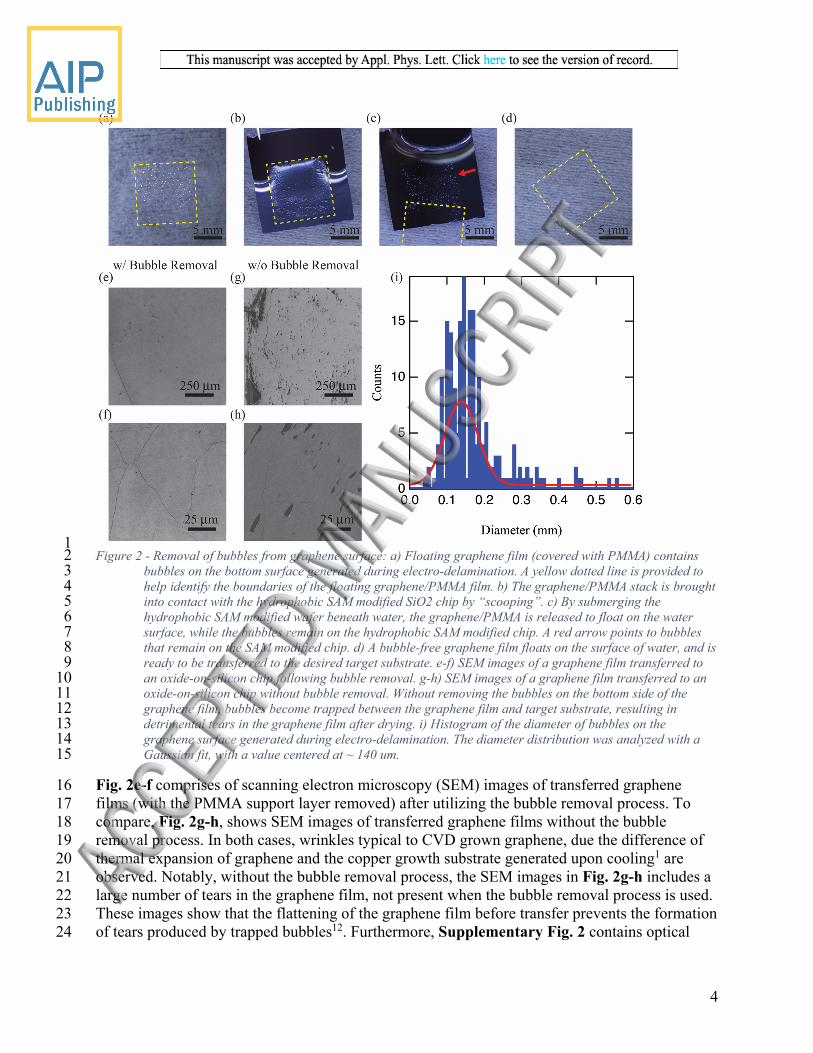
Fig. 2a-d contains optical images of bubble removal from an actual graphene film. Fig. 2a shows 8 a floating graphene/PMMA film with bubbles on the bottom clearly evident. A yellow dotted 9 line was added to help identify the boundary of the film. In Fig. 2b, the graphene/PMMA film is 10 “scooped” from DI water using the hydrophobic modified substrate, with half of the film still 11 floating in DI water, while the other half is “pinned” to the substrate. After the film makes full 12 contact with the hydrophobic substrate, the substrate is immersed back into DI water to release 13 the film, allowing the graphene to float to the surface of DI water. Even as the graphene/PMMA 14 film floats away, the square imprint of the bubbles is apparent on the hydrophobic substrate, 15 highlighted by the red arrow in Fig. 2c. Upon exposing the hydrophobic substrate to air, the 16 bubbles can be simply popped, and hence, the substrate can be readily reused for further bubble 17 removal from the graphene film. Because the amount of bubbles removed can depend on the 18 operational proficiency of the “scooping” method, to improve the efficacy of the method, the 19 bubble removal procedure is repeated on the same film three additional times, each time rotating 20 the graphene film by 90 degrees. We found that repeating the bubble removal process three 21 additional times was sufficient to fully remove all bubbles from the graphene surface. Fig. 2d 22 shows the floating graphene/PMMA film with all bubbles removed, ready for transfer to the 23 desired target substrate. 24
4
1 Figure 2 - Removal of bubbles from graphene surface: a) Floating graphene film (covered with PMMA) contains 2
bubbles on the bottom surface generated during electro-delamination. A yellow dotted line is provided to 3 help identify the boundaries of the floating graphene/PMMA film. b) The graphene/PMMA stack is brought 4 into contact with the hydrophobic SAM modified SiO2 chip by “scooping”. c) By submerging the 5 hydrophobic SAM modified wafer beneath water, the graphene/PMMA is released to float on the water 6 surface, while the bubbles remain on the hydrophobic SAM modified chip. A red arrow points to bubbles 7 that remain on the SAM modified chip. d) A bubble-free graphene film floats on the surface of water, and is 8 ready to be transferred to the desired target substrate. e-f) SEM images of a graphene film transferred to 9 an oxide-on-silicon chip following bubble removal. g-h) SEM images of a graphene film transferred to an 10 oxide-on-silicon chip without bubble removal. Without removing the bubbles on the bottom side of the 11 graphene film, bubbles become trapped between the graphene film and target substrate, resulting in 12 detrimental tears in the graphene film after drying. i) Histogram of the diameter of bubbles on the 13 graphene surface generated during electro-delamination. The diameter distribution was analyzed with a 14 Gaussian fit, with a value centered at ~ 140 um. 15
Fig. 2e-f comprises of scanning electron microscopy (SEM) images of transferred graphene 16 films (with the PMMA support layer removed) after utilizing the bubble removal process. To 17 compare, Fig. 2g-h, shows SEM images of transferred graphene films without the bubble 18 removal process. In both cases, wrinkles typical to CVD grown graphene, due the difference of 19 thermal expansion of graphene and the copper growth substrate generated upon cooling1 are 20 observed. Notably, without the bubble removal process, the SEM images in Fig. 2g-h includes a 21 large number of tears in the graphene film, not present when the bubble removal process is used. 22 These images show that the flattening of the graphene film before transfer prevents the formation 23 of tears produced by trapped bubbles12. Furthermore, Supplementary Fig. 2 contains optical 24

5
photographs of transfers with and without bubble removal. Large-scale wrinkles in the graphene 1 film, caused by the trapping of bubbles between the graphene film and target substrate film (not 2 from the CVD cooling process), are clearly evident in the case when bubbles are not removed. 3 4 Using the optical image in Fig. 2a, we estimate the size of bubbles removed using image analysis 5 software. The bubble diameter distribution is plotted in Fig. 2i, and a Gaussian fit yields a 6 diameter centered at ~ 140 um, although a tail of large bubbles is present, with ~ 23% of bubbles 7 > 0.20 mm (the 1threshold). However, nanoscale tears in Fig. 2h suggest that nanoscale 8 bubbles that exist on the graphene surface are removed with the bubble removal process, but we 9 have not confirmed this with nano-imaging. Nonetheless, the removal of micro-scale to mm-10 scale bubbles effectively decreases micro-scale to mm-scale tears and wrinkles in the graphene 11 film. 12 13 In order to investigate the effects of removing micro-scale to mm-scale bubbles on the graphene 14 device performance, we perform a variety of large-area (mm-scale) characterization. The large-15 area measurements allow us to probe collective device behavior that, elsewise, could be 16 undetectable at micro-scale dimensions. Following transfer to an oxide on Si wafer (and PMMA 17 removal), we deposit chromium/gold contacts to probe the graphene electrical properties. Fig. 3a 18 shows the large-area source-drain current versus gate voltage of devices of dimensions ~ 7 x 4.5 19 mm with and without prior bubble removal. Although the charge neutral point voltage (VCNP) is 20 nearly identical for both cases, removing bubbles from the graphene surface results in increased 21 large-area field-effect mobility compared to when bubbles are not removed, as evident in the 22 depletion curve data. We define the on/off ratio as ratio of the current at 0 Vg to the current at 23 VCNP; the on/off ratio is ~ 10 (2x larger than when bubble removal is not used), consistent with 24
increased mobility, Supplementary Table 1. Using the equation, , where IDS 25
is the measured source-drain current, VDS is the applied source-drain voltage, L is the device 26 length, W is the device width, Cox is the oxide capacitance, and Vg is the gate voltage applied, we 27 calculate the large-area field-effect mobility22. The greatest field-effect hole mobility calculated 28 for large-area devices is ~ 3260 cm2 V-1 s-1 (compared to ~ 868 cm2 V-1 s-1 without bubble 29 removal). 30 31 We also measured the large-area (zero gate biased) sheet resistance to quantify the effects of 32 removing bubbles before transfer. We used a shadow mask to deposit four contact electrodes 33 separated by 5 mm in a square geometry to ensure that probed area is equivalent for each device. 34 Supplementary Table 1 lists the sheet resistance values for devices with and without bubble 35 removal. For devices with and without bubble removal, the average sheet resistance is ~ 705 36 / and ~ 1289 /, respectively. The lowest sheet resistance values obtained is ~ 466 / 37 when bubbles are removed, and ~ 1277 / when bubbles are not removed prior to device 38 fabrication. The combination of increased large-area mobility and decreased large-area sheet 39 resistance confirm that electrical quality of graphene devices is improved by the bubble removal 40 process. 41

6
1 Figure 3 – Large-area characterization of devices with bubble removal: a) The source-drain current versus gate 2
voltage is measured over large-areas (mm-scale) for devices with and without bubble removal. With bubble 3 removal, the on/off ratio is increased to ~ 10. b) Representative Raman spectra of transferred graphene 4 films with and without bubble removal. c-d) Raman mapping data of the I[2D]/I[G] for devices fabricated 5 both without and with bubble removal. Cracks and tears in the graphene film from trapped bubbles during 6 transfer are apparent. e) Histograms of the I[2D]/I[G] for graphene films with and without bubble 7 removal. f) Histograms of the D peak intensity for graphene films with and without bubble removal 8
7
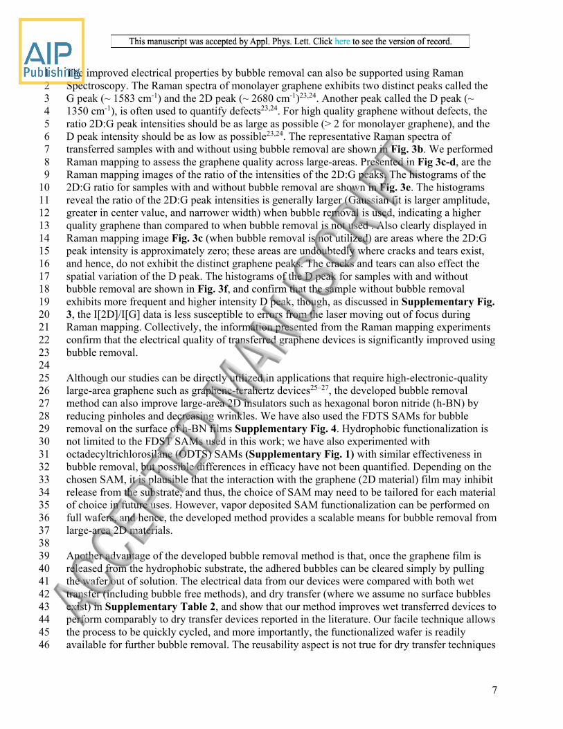
The improved electrical properties by bubble removal can also be supported using Raman 1 Spectroscopy. The Raman spectra of monolayer graphene exhibits two distinct peaks called the 2 G peak (~ 1583 cm-1) and the 2D peak (~ 2680 cm-1)23,24. Another peak called the D peak (~ 3 1350 cm-1), is often used to quantify defects23,24. For high quality graphene without defects, the 4 ratio 2D:G peak intensities should be as large as possible (> 2 for monolayer graphene), and the 5 D peak intensity should be as low as possible23,24. The representative Raman spectra of 6 transferred samples with and without using bubble removal are shown in Fig. 3b. We performed 7 Raman mapping to assess the graphene quality across large-areas. Presented in Fig 3c-d, are the 8 Raman mapping images of the ratio of the intensities of the 2D:G peaks. The histograms of the 9 2D:G ratio for samples with and without bubble removal are shown in Fig. 3e. The histograms 10 reveal the ratio of the 2D:G peak intensities is generally larger (Gaussian fit is larger amplitude, 11 greater in center value, and narrower width) when bubble removal is used, indicating a higher 12 quality graphene than compared to when bubble removal is not used . Also clearly displayed in 13 Raman mapping image Fig. 3c (when bubble removal is not utilized) are areas where the 2D:G 14 peak intensity is approximately zero; these areas are undoubtedly where cracks and tears exist, 15 and hence, do not exhibit the distinct graphene peaks. The cracks and tears can also effect the 16 spatial variation of the D peak. The histograms of the D peak for samples with and without 17 bubble removal are shown in Fig. 3f, and confirm that the sample without bubble removal 18 exhibits more frequent and higher intensity D peak, though, as discussed in Supplementary Fig. 19 3, the I[2D]/I[G] data is less susceptible to errors from the laser moving out of focus during 20 Raman mapping. Collectively, the information presented from the Raman mapping experiments 21 confirm that the electrical quality of transferred graphene devices is significantly improved using 22 bubble removal. 23 24 Although our studies can be directly utilized in applications that require high-electronic-quality 25 large-area graphene such as graphene-terahertz devices25–27, the developed bubble removal 26 method can also improve large-area 2D insulators such as hexagonal boron nitride (h-BN) by 27 reducing pinholes and decreasing wrinkles. We have also used the FDTS SAMs for bubble 28 removal on the surface of h-BN films Supplementary Fig. 4. Hydrophobic functionalization is 29 not limited to the FDST SAMs used in this work; we have also experimented with 30 octadecyltrichlorosilane (ODTS) SAMs (Supplementary Fig. 1) with similar effectiveness in 31 bubble removal, but possible differences in efficacy have not been quantified. Depending on the 32 chosen SAM, it is plausible that the interaction with the graphene (2D material) film may inhibit 33 release from the substrate, and thus, the choice of SAM may need to be tailored for each material 34 of choice in future uses. However, vapor deposited SAM functionalization can be performed on 35 full wafers, and hence, the developed method provides a scalable means for bubble removal from 36 large-area 2D materials. 37 38 Another advantage of the developed bubble removal method is that, once the graphene film is 39 released from the hydrophobic substrate, the adhered bubbles can be cleared simply by pulling 40 the wafer out of solution. The electrical data from our devices were compared with both wet 41 transfer (including bubble free methods), and dry transfer (where we assume no surface bubbles 42 exist) in Supplementary Table 2, and show that our method improves wet transferred devices to 43 perform comparably to dry transfer devices reported in the literature. Our facile technique allows 44 the process to be quickly cycled, and more importantly, the functionalized wafer is readily 45 available for further bubble removal. The reusability aspect is not true for dry transfer techniques 46
8
that use of non-reusable materials such as thermal release tape17,18. We have used one single 1 functionalized wafer for repeated bubble removal without noticeable degradation over 100 times. 2 3 We have developed a scalable and reusable bubble removal method using hydrophobic 4 functionalized surfaces that reduce tears and wrinkles created by trapped bubbles between 5 transferred graphene films and the target substrate to improve the large-area electronic quality of 6 graphene devices. We confirm that the developed bubble removal method results in improved 7 large-area mobility (device on/off ratio), and decreased (zero gate-biased) sheet resistance. 8 Following bubble removal, the high-quality graphene was also confirmed using Raman 9 spectroscopy mapping, and shows increased 2D:G peak ratio and decreased the D peak intensity 10 across large areas. Our bubble removal method could find wide use in applications such as large-11 area 2D optoelectronics, and wafer-scale fabrication of 2D heterojunction devices. 12 13
Methods: 14 SAM Functionalization of Substrate: 15 A SiO2 on Si wafer is first cleaned in hot piranha at 120 C for one hour. Following piranha clean, 16 the hydrophilic wafer is rinsed with DI water and dried. Then, the wafer is placed in a vacuum 17 chamber with ~ 50 uL of FDTS solution in a glass vial. The chamber is evacuated, then sealed. 18 After 6 hours, the wafer is removed, and hydrophobic functionalization is confirmed by water 19 contact angle. 20 21 CVD Graphene Growth: 22 Large-domain monolayer graphene films are grown on copper foils by low pressure chemical 23 vapor deposition in an evacuated 5-inch quartz tube using a fast, oxygen-assisted growth process 24 following Ref [20]. Briefly, at 1030 C, two-stages of methane flow (0.8 sccm and 2.4 sccm) are 25 used to control graphene nucleation density and edge growth until individual domains merge to 26 form a full film. 27 28 Graphene and H-BN Transfer: 29 Following CVD growth, graphene films on copper foil are covered with a layer of PMMA and 30 baked. The backside graphene is then removed in O2 plasma, and the sample is placed in a 60 C 31 oven overnight. Samples are cut to ~ 1.5 x 1.5 cm squares for transfer. The graphene/PMMA 32 stack is delaminated from the copper foil in a 0.2 M NaOH solution using 2.7 V between the 33 graphene sample and a carbon rod. The delamination process generates bubbles that stick to the 34 bottom side of the floating graphene/PMMA stack. Following delamination, the 35 graphene/PMMA stack can be wet transferred to the desired target substrate. In this work, the 36 substrate is 10 nm Al2O3 deposited via atomic layer deposition (ALD) on 90 nm SiO2 on a high 37 resistivity silicon (Si) substrate. The PMMA layer is removed in acetone. H-BN films purchased 38 from graphene-supermarket are transferred using the same protocol. 39 40 Electrical Characterization: 41 Four Cr/Au (20/50 nm) electrodes were deposited by electron beam evaporation in a square 42 layout separated by 5 mm width for electrical characterization. Large-area sheet resistance 43 measurements were performed using a 4-point van der Pauw method with a lock-in amplifier. 44

9
Depletion curve measurements were performed on diagonally opposed contacts as the source-1 drain electrodes (separated by ~ 7 mm) with the gate voltage applied to the silicon layer. 2 3 SEM Imaging: 4 SEM images were obtained using a FEI Magellan 400 XHR SEM. Imaging was performed using 5 1 kV acceleration voltage, and 0.1 nA beam current. 6 7 Raman Mapping: 8 Raman spectroscopy was performed using a Renishaw InVia Raman Spectrometer with a 532 9 nm laser. Raman mapping was performed in a ~ 3x3 mm area, with 60 um step size and 0.7 10 second acquisition time. Peak fitting was performed using the Renishaw WiRE software. The 11 extracted peak fitting was plotted using Igor Pro 7. 12 13 Bubble Analysis: 14 Optical photographs of graphene films with bubbles were imaged using an 18-megapixel Canon 15 EOS 650 D with a 100mm macro lens. The diameter of the bubbles was estimated using ImageJ 16 software, with the scale calibrated to 1 mm. Gaussian fitting of the diameter size was performed 17 using Igor Pro 7. 18 19 Supplementary Information including contact angle, large scale wrinkle characterization, 20 Raman focusing procedure, H-BN transfer, and electrical data is linked to the online version of 21 the paper. 22 23 Acknowledgements 24 We appreciate the conversations with D. Fishman, J. Hes, and S. Martinez. SEM, and oxygen 25 plasma work was performed at the Irvine Materials Research Institute (IMRI). Raman 26 spectroscopy work was performed at the UC Irvine Laser Spectroscopy Facility (LSF). CVD 27 synthesis and e-beam evaporation was performed at the Integrated Nanosystems Research 28 Facility (INRF). 29 30 Funding Information 31 This work was funded by the Army Research Office through the ARO-MURI Program and an 32 ARO-Core Grant (Contract No: W911NF-11-1-0024 and W911NF-09-1-0319). 33 34 The authors declare no competing financial interest. 35 36 Correspondence and requests for materials should be addressed to [email protected] 37 38

10
References 1 2
1 X. Li, W. Cai, J. An, S. Kim, J. Nah, D. Yang, R. Piner, A. Velamakanni, I. Jung, E. Tutuc, 3 S.K. Banerjee, L. Colombo, and R.S. Ruoff, Science 324, 1312 (2009). 4 2 C. Mattevi, H. Kim, and M. Chhowalla, J. Mater. Chem. 21, 3324 (2011). 5 3 T. Liang, C. Luan, H. Chen, and M. Xu, Nanoscale 9, 3719 (2017). 6 4 K.K. Liu, W. Zhang, Y.H. Lee, Y.C. Lin, M.T. Chang, C.Y. Su, C.S. Chang, H. Li, Y. Shi, H. 7 Zhang, C.S. Lai, and L.J. Li, Nano Lett. 12, 1538 (2012). 8 5 Y. Zhan, Z. Liu, S. Najmaei, P.M. Ajayan, and J. Lou, Small 8, 966 (2012). 9 6 L. Song, L. Ci, H. Lu, P.B. Sorokin, C. Jin, J. Ni, A.G. Kvashnin, D.G. Kvashnin, J. Lou, B.I. 10 Yakobson, and P.M. Ajayan, Nano Lett. 10, 3209 (2010). 11 7 Y. Chen, X.L. Gong, and J.G. Gai, Adv. Sci. 3, 1 (2016). 12 8 M. Chen, R.C. Haddon, R. Yan, and E. Bekyarova, Mater. Horizons 4, 1054 (2017). 13 9 J.W. Suk, A. Kitt, C.W. Magnuson, Y. Hao, S. Ahmed, J. An, A.K. Swan, B.B. Goldberg, and 14 R.S. Ruoff, ACS Nano 5, 6916 (2011). 15 10 C.T. Cherian, F. Giustiniano, I. Martin-Fernandez, H. Andersen, J. Balakrishnan, and B. 16 Özyilmaz, Small 11, 189 (2015). 17 11 Y. Wang, Y. Zheng, X. Xu, E. Dubuisson, Q. Bao, J. Lu, and K.P. Loh, ACS Nano 5, 9927 18 (2011). 19 12 T. Hallam, N.C. Berner, C. Yim, and G.S. Duesberg, Adv. Mater. Interfaces 1, 1400115 20 (2014). 21 13 X. Liang, B.A. Sperling, I. Calizo, G. Cheng, C.A. Hacker, Q. Zhang, Y. Obeng, K. Yan, H. 22 Peng, Q. Li, X. Zhu, H. Yuan, A.R. Hight Walker, Z. Liu, L.M. Peng, and C.A. Richter, ACS 23 Nano 5, 9144 (2011). 24 14 F. Pizzocchero, B.S. Jessen, P.R. Whelan, N. Kostesha, S. Lee, J.D. Buron, I. Petrushina, M.B. 25 Larsen, P. Greenwood, W.J. Cha, K. Teo, P.U. Jepsen, J. Hone, P. Bøggild, and T.J. Booth, 26 Carbon 85, 397 (2015). 27 15 P. Attard, Langmuir 12, 1693 (1996). 28 16 J. Rafiee, X. Mi, H. Gullapalli, A.V.A.V.A. Thomas, F. Yavari, Y. Shi, P.M. Ajayan, and N.A. 29 Koratkar, Nat. Mater. 11, 217 (2012). 30 17 S. Bae, H. Kim, Y. Lee, X. Xu, J.S. Park, Y. Zheng, J. Balakrishnan, T. Lei, H. Ri Kim, Y. Il 31 Song, Y.J. Kim, K.S. Kim, B. Özyilmaz, J.H. Ahn, B.H. Hong, and S. Iijima, Nat. Nanotechnol. 32 5, 574 (2010). 33 18 J. Kang, S. Hwang, J.H. Kim, M.H. Kim, J. Ryu, S.J. Seo, B.H. Hong, M.K. Kim, and J.B. 34 Choi, ACS Nano 6, 5360 (2012). 35 19 S.J. Kim, T. Choi, B. Lee, S. Lee, K. Choi, J.B. Park, J.M. Yoo, Y.S. Choi, J. Ryu, P. Kim, J. 36 Hone, and B.H. Hong, Nano Lett. 15, 3236 (2015). 37 20 P.H.Q. Pham, W. Zhou, N. V. Quach, J. Li, J.-G. Zheng, and P.J. Burke, Chem. Mater. 28, 38 6511 (2016). 39 21 L. Gao, G.-X. Ni, Y. Liu, B. Liu, A.H. Castro Neto, and K.P. Loh, Nature 505, 190 (2014). 40 22 F. Schwierz, Nat. Nanotechnol. 5, 487 (2010). 41 23 A.C. Ferrari, J.C. Meyer, V. Scardaci, C. Casiraghi, M. Lazzeri, F. Mauri, S. Piscanec, D. 42 Jiang, K.S. Novoselov, S. Roth, and A.K. Geim, Phys. Rev. Lett. 97, 187401 (2006). 43 24 A. Das, S. Pisana, B. Chakraborty, S. Piscanec, S.K. Saha, U. V. Waghmare, K.S. Novoselov, 44 H.R. Krishnamurthy, A.K. Geim, A.C. Ferrari, and A.K. Sood, Nat. Nanotechnol. 3, 210 (2008). 45 25 B. Sensale-Rodriguez, R. Yan, M.M. Kelly, T. Fang, K. Tahy, W.S. Hwang, D. Jena, L. Liu, 46
11
and H.G. Xing, Nat. Commun. 3, 780 (2012). 1 26 J.D. Buron, F. Pizzocchero, P.U. Jepsen, D.H. Petersen, J.M. Caridad, B.S. Jessen, T.J. Booth, 2 and P. Bøggild, Sci. Rep. 5, 12305 (2015). 3 27 P.H.Q. Pham, W. Zhang, N. V. Quach, J. Li, W. Zhou, D. Scarmardo, E.R. Brown, and P.J. 4 Burke, Nat. Commun. 8, 2233 (2017). 5 6


