scanning electron microscopy (sem) - universitas...
TRANSCRIPT

Scanning Electron Microscopy
(SEM)

Content• Brief history and introduction
• Applications
• Instrumentation/components
• Formation of an image
• Electron beam-sample interactions
• Signals that can be used to characterize the microstructure
– Secondary electrons
– Backscattered electrons
– X-rays
• Energy Dispersive X-Ray Microanalysis (EDX / EDS)
• Resolution
• Sample preparation
• Summary

Invented by Ernst Ruska a German physicist (1933)
He was awarded the Nobel Prize for physics for his invention in 1986
History
First SEM – debuted in 1938 by Manfred Von Ardenne
In 1965, Cambridge Scientific Instrument (UK) &
JOEL (Japan) first commercialized SEM individually


COMPARISON OF
THE SIZE OF
OBJECTS

Applications of SEM
1. Topography: the surface features of the sample
2. Morphology: the shape and size of the sample
3. Composition: the elements that the sample is
composed of and their relative amount (%) – purity
4. Crystallographic info: how atoms are arrange in the
sample
Electron microscopes are scientific instruments that use a
beam of highly energetic electrons to examine objects on
a very fine scale.


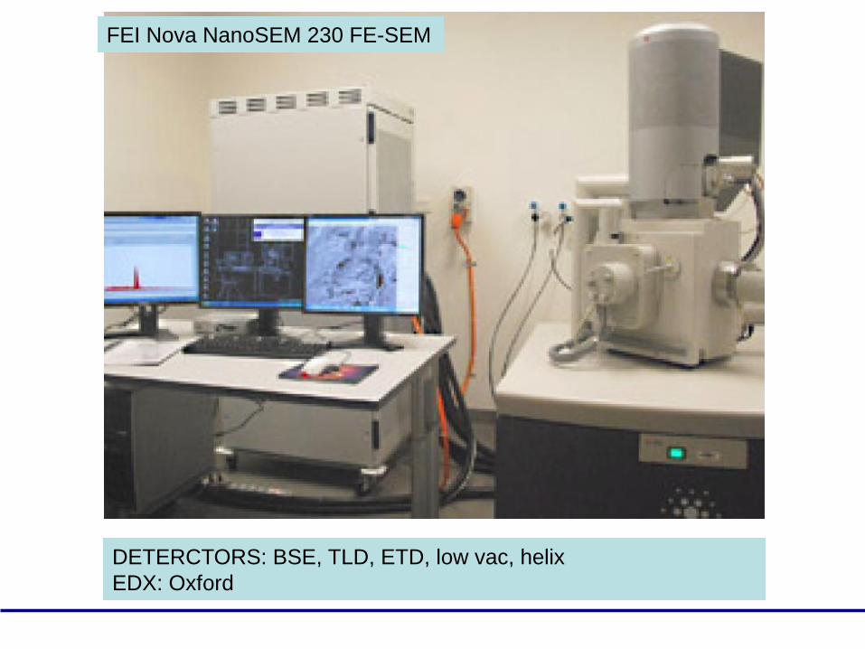
FEI Nova NanoSEM 230 FE-SEM
DETERCTORS: BSE, TLD, ETD, low vac, helix
EDX: Oxford

The instrument


Image formation
We shoot high-energy electrons and analyze the
outgoing electrons/x-rays
Electrons inElectrons out
or: x-rays out

How do we get an image?
156 electrons!
Image
Detector
Electron gun288 electrons!
Sample Area of the sample scan Signal/image formed


SEM micrograph of a chloroplast in maize (Zea mays) showing thylakoids
(green) and assimilation starch granules (grey). (Prepared by freeze
fracturing; micrograph is pseudo-colored.) (Source: G. Wanner LMU)

LOTUS LEAF

SE = from the surface of
the sample
BSE= from the surface of
the sample
and from deeper within the
sample
BSE are reflected electron
The image in SEM is
mapping out the density
of the sample surface
BSE that get trapped in the sample
caused the x-ray to be given off
Electron beam-
sample
interactions

Electron beam-sample interactions• The incident electron beam is scattered in the sample, both
elastically and inelastically
• This gives rise to various signals that we can detect
• Interaction volume increases with increasing acceleration voltage and decreases with increasing atomic number

Backscattered electrons (BSE)• A fraction of the incident
electrons is retarded by
the electro-magnetic field
of the nucleus and if the
scattering angle is greater
than 180 °C the electron
can escape from the
surface• High energy electrons (elastic
scattering)
• Fewer BSE than SE

Factors that affect BSE emission
• Direction of the irritated surface
– more electrons will hit the BSE detector when the surface is aligned towards the BSE detector
• Average atomic number (Z)
• When you want to study differences in atomic numbers the sample should be as levelled as possible (sample preparation is an issue!)

SE vs BSE
SE and BSE SEM images of triangular precipitates at grain boundary of
SnMnNb 0.05 sample.
BSE can observe that the material consists of 2 distinct phases; the bright
grains being composed by a phase with average atomic number higher than
the dark triangular precipitates.

X-rays
• Photons not electrons
• Each element has a fingerprint X-ray signal
• Poorer spatial resolution than BSE and SE
• Relatively few X-ray signals are emitted and the detector is inefficient
relatively long signal collecting times are needed

X-rays
• Most common spectrometer: EDS
(energy-dispersive spectrometer)
• Signal overlap can be a problem
• We can analyze our sample in different
modes
– spot analysis
– line scan
– chemical concentration map
(elemental mapping)

Electron guns
• We want many electrons per time unit per area (high current density) and as small electron spot as possible
• Traditional guns: thermionic electron gun (electrons are emitted when a solid is heated)– W-wire, LaB6-crystal
• Modern: field emission guns (FEG) (cold guns, a strong electric field is used to extract electrons)– Single crystal of W, etched to a
thin tip
FEG – gives FESEM

Electron guns• Using field emission guns (FEG) - we get a
smaller spot and higher current densities compared to thermionic guns
• But we need better vacuum for a FEG
Single crystal of LaB6Tungsten wire Field emission tip

Detectors
Secondary electron (SE)
detector:
(Everhart-Thornley)
Backscattered electron
(BSE) detector (Solid-State
Detector)

Traditional detectors
• Secondary electrons (SE): Everhart-Thornley
Detector (ETD)
• Backscattered electrons (BSE): Solid State
Detector
• X-rays: Energy dispersive spectrometer (EDS)

Vacuum• The electron beam generated by the electron gun would
encounter interference from air particles in the atmosphere.
• these particles block the path of the electron beam, they
would also be knocked out of the air and onto the specimen,
which would distort the surface of the specimen.
Vacuum requirements is dependant of the type of detector
• Chemical (corrosion) and thermal stability is necessary for a
well-functioning filament (gun pressure)
– A field emission gun requires ~ 10-10 Torr
– LaB6: ~ 10-6 Torr


CHARGE-UP: can be
prevented by coating the
non-conductor sample
with metal (conductor) –
allowing the charge on the
sample surface go to
ground through the coated
conductive film


St/MMA=2
Eg 1
St/MMA=4
St/MMA=3.5 St/MMA=5
FESEM for samples prepared at various St/MMAs = 2-5
Topography and morphology

Shape-stabilised n-octadecane-AC-
nanocomposites - 3D
3D
activated carbon with 3D pores
Activated carbon derived from peat soil as a framework for the
preparation of shape-stabilized phase change material, T Khadiran,
MZ Hussein, Z Zainal, R Rusli, Energy 2015 (82), 468-478.
Eg 2

Shape-stabilised n-octadecane-AC-
nanocomposites
Palm Kernel Shell Activated Carbon as an Inorganic
Framework for Shape-Stabilized Phase Change Material
Nicholas et al., Nanomaterials 2018, 8, 689
PKS C20SSPCM-C20
Eg 3
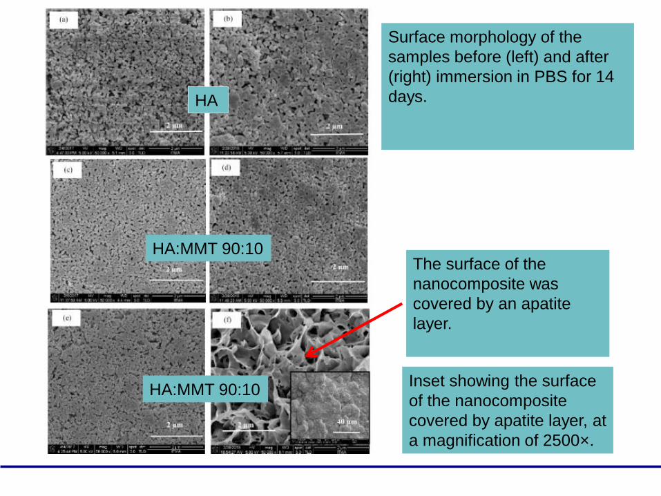
Surface morphology of the
samples before (left) and after
(right) immersion in PBS for 14
days. HA
HA:MMT 90:10
HA:MMT 90:10
The surface of the
nanocomposite was
covered by an apatite
layer.
Inset showing the surface
of the nanocomposite
covered by apatite layer, at
a magnification of 2500×.


Environmental SEM: ESEM
• Traditional SEM chamber pressure:
~ 10-6 Torr
• ESEM: 0.08 – 30 Torr
• Various gases can be used
• Requires different SE detector

Why ESEM?
• To image challenging samples such as:
– insulating samples
– vacuum-sensitive samples (e.g. biological samples)
– irradiation-sensitive samples (e.g. thin organic films)
– “wet” samples (oily, dirty, greasy)
• To study and image chemical and physical
processes in-situ such as:
– mechanical stress-testing
– oxidation of metals
– hydration/dehydration (e.g. watching paint dry)

Resolution
• Best resolution that can be obtained: size of the electron spot on the sample surface– The introduction of FEG has dramatically improved
the resolution of SEM’s
• The volume from which the signal electrons are formed defines the resolution– SE image has higher resolution than a BSE image
• Scanning speed: – a weak signal requires slow speed to improve signal-
to-noise ratio
– when doing a slow scan drift in the electron beam can affect the accuracy of the analysis

Energy Dispersive X-Ray
Microanalysis (EDX/EDS)

An EDX spectrum was collected at each
point identified in the top secondary electron
image to individually characterize the
wires. The resulting spectra show that the
largest diameter wire (spot 1) is Ni, the
medium diameter wire (spot 2) is Al, and the
thinnest diameter wire (spot 3) is Ti. Note
that a small amount of Al smeared onto the
other wire surfaces when these wires were
wound together

x-ray mapping of elements.
The original secondary electron
image of the three twisted wires
is shown again, this time
overlaid with the color-coded
element maps corresponding to
the different wires shown in this
field of view. The individual
element maps are also shown.

Summary
• SEM is a versatile instrument for many applications especially for the study of surface morphology.
• To get a micrograph, an electron probe is scanned across the surface of the sample and detectors interpret the signal as a function of time.
• A resolution of 1 – 2 nm can be obtained when operated in a high resolution setup.
• The introduction of ESEM and the field emission gun have simplified the imaging of challenging samples

Summary
• Signals:
– Secondary electrons (SE): mainly topography
• Low energy electrons, high resolution
• Surface signal dependent on curvature
– Backscattered electrons (BSE): mainly chemistry
• High energy electrons
• “Bulk” signal dependent on atomic number
– X-rays (EDX): chemistry• microanalysis

Take home keywords
• SEM, ESEM and FESEM
• Topography, morphology, composition Instrumentation/components: Electron gun, lens (condenser and objective), deflection coil, sensors/detectors, TLD, ETD
(Everhart-Thornley) for SE, BSE, etc.
• Formation of an image: scanning of electron
• Electron beam-sample interactions: SE, BSE and x-ray
• Energy Dispersive X-Ray Microanalysis (EDX / EDS), elemental mapping
• Resolution
• Sample preparation