scanning probe investigations of nanopatterned and thermo
TRANSCRIPT

Louisiana State UniversityLSU Digital Commons
LSU Doctoral Dissertations Graduate School
2015
Scanning Probe Investigations of Nanopatternedand Thermo-responsive Polypeptoids and theDesign of a Sample Stage for Force ModulationMicroscopyLu LuLouisiana State University and Agricultural and Mechanical College, [email protected]
Follow this and additional works at: https://digitalcommons.lsu.edu/gradschool_dissertations
Part of the Chemistry Commons
This Dissertation is brought to you for free and open access by the Graduate School at LSU Digital Commons. It has been accepted for inclusion inLSU Doctoral Dissertations by an authorized graduate school editor of LSU Digital Commons. For more information, please [email protected].
Recommended CitationLu, Lu, "Scanning Probe Investigations of Nanopatterned and Thermo-responsive Polypeptoids and the Design of a Sample Stage forForce Modulation Microscopy" (2015). LSU Doctoral Dissertations. 1662.https://digitalcommons.lsu.edu/gradschool_dissertations/1662
SCANNING PROBE INVESTIGATIONS OF NANOPATTERNED AND THERMO-
RESPONSIVE POLYPEPTOIDS AND THE DESIGN OF A SAMPLE STAGE FOR FORCE
MODULATION MICROSCOPY
A Dissertation
Submitted to the Graduate Faculty of the
Louisiana State University and
Agricultural and Mechanical College
in partial fulfillment of the
requirements for the degree of
Doctor of Philosophy
in
The Department of Chemistry
by
Lu Lu
B.S., University of Science and Technology of China, 2010
August 2015

ii
ACKNOWLEDGEMENTS
I would like to express my thanks to my two advisors, Dr. Jayne C. Garno and Dr. Donghui
Zhang, for their guidance and support during my Ph.D career at Louisiana State University. I want
to thank my committee members Dr. Bin Chen, Dr. Francisco Hung, and Dr. Graca Vicente for
reviewing my dissertation and providing valuable feedback.
I would like to thank Dr. Song Xu from Keysight Technologies for collaboration and
helpful discussion.
I also thank both past and current members of the Garno and Zhang groups, for the great
times we had together for the past five years.
Lastly, I want to express my deepest appreciation to my parents, my sister and my husband
for their support and love.
iii
TABLE OF CONTENTS
ACKNOWLEDGEMENTS ............................................................................................................ ii
LIST OF ABBREVIATIONS ........................................................................................................ vi
ABSTRACT ................................................................................................................................. viii
CHAPTER 1. INTRODUCTION ................................................................................................... 1
1.1 Nanoscale Surface Studies with Atomic Force Microscopy ................................................. 1
1.2 Surface Patterning of Polypeptoids Using Particle Lithography .......................................... 1
1.3 In Situ Studies of the Thermo-Responsiveness of Polypeptoid Nanopillars ......................... 2
1.4 Review of Previous Studies with Force Modulation Microscopy......................................... 3
1.5 A Force Modulation Sample Stage for Scan-by-Tip AFM ................................................... 3
1.6 Stage-Driven Force Modulation Microscopy versus Tip-Driven Indirect Magnetic
Modulation .................................................................................................................................. 4
1.7 Conclusions and Future Prospectus ....................................................................................... 4
CHAPTER 2. EXPERIMENTAL DESIGNS WITH SCANNING PROBE MICROSCOPY ....... 5
2.1 Background and Imaging Principle of Atomic Force Microscopy ....................................... 5
2.2 Contact-mode and Lateral Force Imaging ............................................................................. 6
2.3 AFM Force Spectroscopy...................................................................................................... 9
2.4 Tapping-mode AFM and Phase Imaging ............................................................................ 10
2.5 Force Modulation Microscopy ............................................................................................ 13
2.6 In Situ Temperature Studies Using AFM ............................................................................ 16
2.7 AFM imaging Modes Used in the Dissertation ................................................................... 16
CHAPTER 3. DIRECTED GROWTH OF POLYMER NANOPILLARS USING
SURFACE-INITIATED RING-OPENING POLYMERIZATION OF N-ALLYL N-
CARBOXYANHYDRIDE ........................................................................................................... 18
3.1 Introduction ......................................................................................................................... 18
3.2 Experimental Section .......................................................................................................... 21
3.2.1 Materials and Reagents ................................................................................................. 21
3.2.2 Atomic Force Microscopy ............................................................................................ 21
3.2.3 Preparation of Nanopores within an OTS Film ............................................................ 21
3.2.4 Preparation of APTES Nanodots .................................................................................. 22
3.2.5 Three Steps Synthesis of Allyl-NCA............................................................................ 22
3.2.6 Polymerization of Allyl-NCA. ..................................................................................... 24
3.3 Results and Discussion ........................................................................................................ 24
3.4 Conclusion ........................................................................................................................... 32
CHAPTER 4. THERMO-RESPONSIVE BEHAVIOR OF LINEAR COPOLYPEPTOID
NANOSTRUCTURES INVESTIGATED WITH ATOMIC FORCE MICROSCOPY .............. 33
4.1 Introduction ......................................................................................................................... 33
4.2 Experimental Section .......................................................................................................... 35
4.2.1 Preparation of Nanopatterned UTS Sites ...................................................................... 35
4.2.2 Synthesis of Linear poly[(N-ethyl glycine)32-r-(N-butyl glycine)17] Copolymer ......... 35
iv
4.2.3 Preparation Nanopatterned Poly[(N-ethyl glycine)32-r-(N-butyl glycine)17] by
Surface Thiol-ene Click Reaction .......................................................................................... 36
4.2.4 Thermoresponsive Study of Nanopatterned Copolypeptoids using in situ AFM ......... 36
4.3 Result and Discussion ......................................................................................................... 37
4.4 Conclusion ........................................................................................................................... 43
CHAPTER 5. A REVIEW ON FORCE MODULATION MICROSCOPY AND THE
CAPABILITY OF NANOMECHANICAL MAPPING OF SURFACE ELASTIC AND
VISCOELASTIC PROPERTIES.................................................................................................. 44
5.1 History of Force Modulation Microscopy (FMM) .............................................................. 44
5.2 Instrument Set-up of FMM ................................................................................................. 45
5.3 Advantages of FMM ........................................................................................................... 47
5.4 Studying Self-assembled Monolayers (SAMs) Using FMM .............................................. 49
5.5 Investigating Polymeric Materials Using FMM ................................................................. 53
5.6 Probing Biological and Inorganic Samples Using FMM .................................................... 57
5.7 Conclusions ......................................................................................................................... 59
CHAPTER 6. SAMPLE STAGE DESIGNED FOR FORCE MODULATION
MICROSCOPY USING A TIP-MOUNTED AFM SCANNER .................................................. 60
6.1 Introduction ......................................................................................................................... 60
6.2 Experimental Section .......................................................................................................... 61
6.2.1 Materials and Reagents ................................................................................................. 61
6.2.2 Atomic Force Microscopy ............................................................................................ 62
6.3 Results and Discussion ........................................................................................................ 62
6.3.1 Design of the FMM Sample Stage ............................................................................... 62
6.3.2 Characterization of Nanopatterns within an OTS Film using the FMM Sample
Stage. ..................................................................................................................................... 64
6.3.3 FMM Characterization of Nanorings of PEG-silane .................................................... 67
6.3.4 Characterization of a Cyclic Gel Sample with FMM ................................................... 69
6.4 Conclusions ......................................................................................................................... 72
CHAPTER 7: DIRECT COMPARISON OF SAMPLE ACTUATION VERSUS TIP
VIBRATION CONFIGURATION FOR FORCE MODULATION AFM .................................. 73
7.1 Introduction ......................................................................................................................... 73
7.2 Experiment Section ............................................................................................................. 74
7.2.1 Materials and Reagents ................................................................................................. 74
7.2.2 Atomic Force Microscopy ............................................................................................ 75
7.2.3 Preparation of CMPS Nanorings .................................................................................. 75
7.2.4 Characterization of CMPS Nanorings with Stage-driven FMM. ................................. 76
7.2.5 Characterization of CMPS Nanorings with Tip-driven IMM ...................................... 77
7.3 Results ................................................................................................................................. 77
7.3.1 Nanorings of CMPS Studied with FMM and IMM with and without Sample/Tip
Modulation............................................................................................................................. 77
7.3.2 Nanorings of CMPS Studied with FMM at Selected Driving Frequencies .................. 80
7.3.3 Nanorings of CMPS Studied with IMM at Selected Driving Frequencies ................... 80
7.3.4 High Resolution Stage-driven FMM and Tip-driven IMM Images of CMPS
Nanorings............................................................................................................................... 83
v
7.3.5 Frequency Sweeps of FMM at Selected Regions of the Sample Surface .................... 85
7.3.6 Frequency Sweeps of IMM at Selected Regions of the Sample Surface ..................... 86
7.3.7 Dynamic Stage-driven FMM and Tip-driven IMM Studies ......................................... 87
7.3.8 Side-by-side Comparison of FMM and IMM at the Same Driving Frequencies. ........ 89
7.4 Discussion ........................................................................................................................... 91
7.5 Conclusion ........................................................................................................................... 92
CHAPTER 8. CONCLUSIONS AND FUTURE PROSPECTUS ............................................... 93
REFERENCES ............................................................................................................................. 95
APPENDIX A: PROCEDURE FOR FORCE MODULATION MICROSCOPY (FMM)
USING NEWLY-DESIGNED SAMPLE STAGE ..................................................................... 114
APPENDIX B: PROCEDURE FOR TEMPERATURE STUDIES USING THE
HEATING STAGE WITH KEYSIGHT 5500 OR 5420 ............................................................ 117
APPENDIX C: SUPPLEMENTAL INFORMATION FOR THERMO-RESPONSIVE
BEHAVIOR OF LINEAR COPOLYPEPTOID NANOSTRUCTURES INVESTIGATED
WITH ATOMIC FORCE MICROSCOPY ................................................................................ 119
APPENDIX D: SUPPLEMENTAL INFORMATION FOR SAMPLE STAGE
DESIGNED FOR FORCE MODULATION MICROSCOPY USING A TIP-MOUNTED
AFM SCANNER ........................................................................................................................ 124
APPENDIX E: SUPPLEMENTAL INFORMATION FOR DIRECT COMPARISON OF
SAMPLE ACTUATION VERSUS TIP VIBRATION CONFIGURATION FOR FORCE
MODULATION AFM ................................................................................................................ 127
APPENDIX F: IMAGING POLYSTYRENE LATEX MESOSPHERES USING AFM .......... 133
APPENDIX F: PERMISSIONS ................................................................................................. 134
VITA ........................................................................................................................................... 138
vi
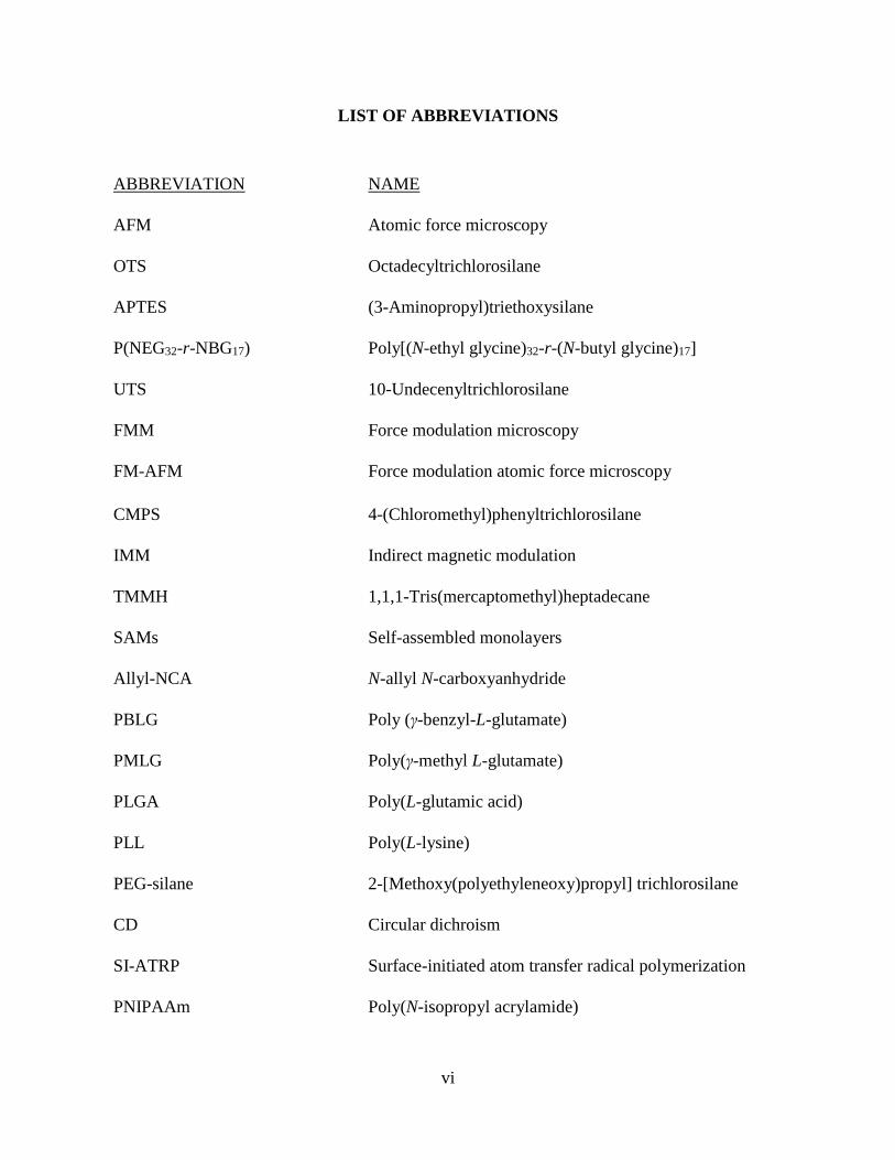
LIST OF ABBREVIATIONS
ABBREVIATION NAME
AFM Atomic force microscopy
OTS Octadecyltrichlorosilane
APTES (3-Aminopropyl)triethoxysilane
P(NEG32-r-NBG17) Poly[(N-ethyl glycine)32-r-(N-butyl glycine)17]
UTS 10-Undecenyltrichlorosilane
FMM Force modulation microscopy
FM-AFM Force modulation atomic force microscopy
CMPS 4-(Chloromethyl)phenyltrichlorosilane
IMM Indirect magnetic modulation
TMMH 1,1,1-Tris(mercaptomethyl)heptadecane
SAMs Self-assembled monolayers
Allyl-NCA N-allyl N-carboxyanhydride
PBLG Poly (γ-benzyl-L-glutamate)
PMLG Poly(γ-methyl L-glutamate)
PLGA Poly(L-glutamic acid)
PLL Poly(L-lysine)
PEG-silane 2-[Methoxy(polyethyleneoxy)propyl] trichlorosilane
CD Circular dichroism
SI-ATRP Surface-initiated atom transfer radical polymerization
PNIPAAm Poly(N-isopropyl acrylamide)
vii
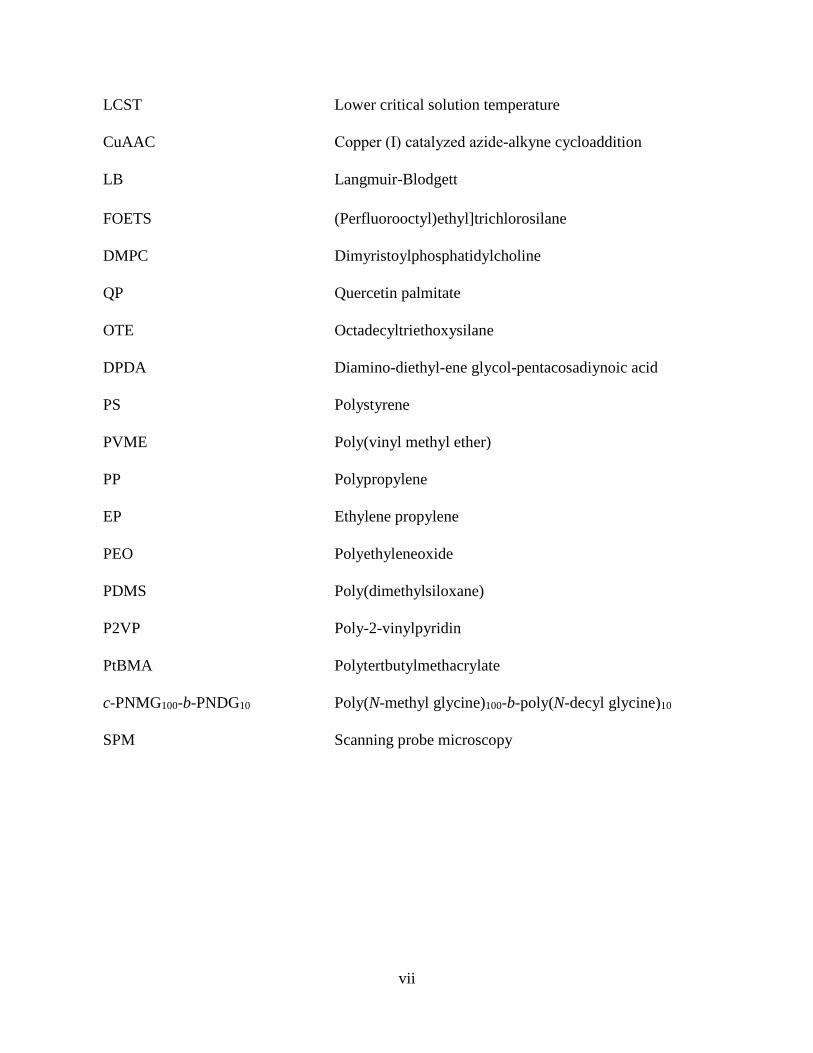
LCST Lower critical solution temperature
CuAAC Copper (Ι) catalyzed azide-alkyne cycloaddition
LB Langmuir-Blodgett
FOETS (Perfluorooctyl)ethyl]trichlorosilane
DMPC Dimyristoylphosphatidylcholine
QP Quercetin palmitate
OTE Octadecyltriethoxysilane
DPDA Diamino-diethyl-ene glycol-pentacosadiynoic acid
PS Polystyrene
PVME Poly(vinyl methyl ether)
PP Polypropylene
EP Ethylene propylene
PEO Polyethyleneoxide
PDMS Poly(dimethylsiloxane)
P2VP Poly-2-vinylpyridin
PtBMA Polytertbutylmethacrylate
c-PNMG100-b-PNDG10 Poly(N-methyl glycine)100-b-poly(N-decyl glycine)10
SPM Scanning probe microscopy
viii
ABSTRACT
Protocols for patterning nanostructures of polymers were developed to enable scanning
probe microscopy (SPM) studies of surface properties at the molecular level. A chemically
selective surface for patterning polymers was generated by combining particle lithography with
organosilane immersion. Poly(N-allyl glycine), a biocompatible and backbone degradable
polypeptoid, was grown on Si(111) at confined amine sites using surface-initiated polymerization
(also known as the “graft from” approach). A thermo-responsive random copolypeptoid, poly[(N-
ethyl glycine)32-r-(N-butyl glycine17)], was pre-synthesized and attached onto a patterned
organosilane surface using a thiol-ene click reaction (“graft to” approach). The phase transitions
of the copolypeptoid nanostructures in an aqueous environment was studied using in situ atomic
force microscopy (AFM). A heated stage was used to heat the nanopatterned sample in liquid
media.
Force modulation microscopy (FMM), one of over 50 possible modes of SPM, is used to
acquire mechanical properties of samples concurrent with topographic information. The history,
instrument set-up, advantages, and applications with self-assembled monolayers, polymers,
biological and inorganic samples are reviewed in this dissertation. The sample is placed directly
on an xyz scanner for the most common FMM configuration. Most commercial SPM systems are
designed to have the tip mounted on the piezotube scanner. To facilitate FMM with tip-mounted
scanners, a sample stage was designed and constructed of machined polycarbonate. A
piezoactuator in the sample stage was used to drive the vibration of the sample in the z-direction
at selected frequency and amplitude. The sample stage was evaluated by studying three samples
with increasing complexity. This sample-driven FMM was compared with indirect magnetic
modulation (IMM), an alternate way to accomplish force modulation studies by modulating the
nosecone assembly. A test platform of patterned nanoring samples was evaluated to systematically

ix
compare FMM and IMM. Both methods can be used to sensitively acquire high resolution images
of sample elasticity. However, the newly designed sample stage for FMM is easier to operate
compared with IMM.
1
CHAPTER 1. INTRODUCTION
Protocols have been developed in this dissertation for studies of polymerization reaction
mechanisms at the molecular level using a surface test platform of patterned polymer nanopillars.
Several imaging modes of atomic force microscopy (AFM) were selected or developed to
investigate systems of interest. A prototype sample stage accessory for AFM was designed and
evaluated to enable advanced measurements with force modulation microscopy.
1.1 Nanoscale Surface Studies with Atomic Force Microscopy
Since the invention of AFM in 1986,1 new studies have been advanced for surface analysis
in fields such as biology,2-4 polymers,5-7 molecular electronics8 and medical diagnostics.9-10 The
resolution of AFM imaging is not limited by the wavelength of light. With an ultra-sharp probe,
the topographic resolution of AFM can achieve 0.1 nm for the x and y directions and 0.01 nm for
the z direction.11-13 More than 50 AFM modes have been developed for imaging and for measuring
forces. The background and imaging principle of scanning probe microscopy and the AFM modes
used for this dissertation are summarized in Chapter 2, including contact-mode, lateral force
imaging, tapping-mode, phase imaging, force modulation microscopy, and indirect magnetic
modulation. Characterizations using AFM force spectroscopy and in situ temperature studies with
a heating stage will also be described.
1.2 Surface Patterning of Polypeptoids Using Particle Lithography
Arrays of polymer nanostructures were prepared on Si(111) using a stepwise chemistry
route combined with particle lithography. In the first step, nanopores were prepared within a thin
film of a self-assembled monolayer of octadecyltrichlorosilane (OTS). The film of OTS served as
a surface resist and the areas of nanopores provided sites for further reactions. The initiator, (3-
aminopropyl)triethoxysilane (APTES) was grown selectively inside the nanopores to define
surface sites for polymerization reaction to proceed. Surface-initiated ring-opening polymerization
2
of N-allyl N-carboxyanhydride with APTES formed polymer pillars on the nanopatterns of
APTES, which terminated with amine functional groups. The surface changes for each step were
monitored using AFM. Slight variations in the height of the poly(N-allyl glycine) pillars were
observed which scale correspondingly to the initial dimensions of nanopores. The distance
between polymer nanopillars is controlled by the size of mesoparticle masks. This platform has
potential application in biotechnology as smart coatings, biosensors or bioseparations based on the
biocompatibility, backbone biodegradability and processability of poly(N-allyl glycine). In
Chapter 3, the strategy of surface patterning of polypeptoids at the nanoscale and the surface
characterizations of each step will be presented.
1.3 In Situ Studies of the Thermo-Responsiveness of Polypeptoid Nanopillars
Nanoscale surface test platforms were used to investigate the phase transitions of thermo-
responsive copolymer nanostructures with AFM. A clear aqueous solution of the random
copolymer poly[(N-ethyl glycine)32-r-(N-butyl glycine)17], abbreviated as P(NEG32-r-NBG17),
becomes turbid upon heating, and upon cooling returns to a clear appearance. The clarity of the
P(NEG32-r-NBG17) solution indicates a response to temperature that is attributable to reversible
polymeric phase transitions. For studies with AFM, nanopores on Si(111) within a film of
octadecyltrichlorosilane (OTS) were prepared using particle lithography combined with steps of
solution immersion. A second silane, 10-undecenyltrichlorosilane (UTS), was backfilled into the
exposed nanopores to form ultra-small surface reactive sites for site-selective polymer deposition
and growth. The random copolymer P(NEG32-r-NBG17) was anchored to reactive sites of UTS
nanodots to produce patterned polymer pillars. The morphology and surface arrangement of
polymer nanopillars were characterized at each step using high resolution AFM. Studies of thermo-
responsive properties were developed to accomplish dynamic protocols in liquid media. A
temperature stage was used to heat the sample during time-lapse AFM imaging. To the best of our
3
knowledge this is the first report using scanning probe studies to characterize the thermo-
responsive properties of patterned polymer pillars as detailed in Chapter 4. Significant advantages
are gained by localizing and patterning polymer pillars on surfaces to enable direct visualization
of surface changes via AFM studies of thermo-responsive properties.
1.4 Review of Previous Studies with Force Modulation Microscopy
A review of force modulation microscopy (FMM) and the capabilities for nanomechanical
mapping of surface elastic and viscoelastic properties is presented in Chapter 5. Force modulation
microscopy was invented in 1991 by Maivald and Hansma et al.14 With FMM, local mechanical
properties of a sample can be acquired along with topographic information. Vibration is applied to
the z axis at the tip-sample contact during contact-mode imaging. A contemporary review of
instrumental configurations for FMM and applications with self-assembled monolayers, polymers,
inorganic materials and biological samples is presented.
1.5 A Force Modulation Sample Stage for Scan-by-Tip AFM
Among the modes of scanning probe microscopy that have been developed, FMM is
commonly used to acquire mechanical properties of samples along with topographic information.
The FMM mode is particularly useful for investigations with polymer samples and organic thin
films. We have designed and tested a sample stage for FMM constructed of machined
polycarbonate. The generic design enables FMM measurements for instrument configurations with
a tip-mounted AFM scanner. A piezoactuator is embedded within the sample stage to drive the
sample to vibrate in the z-direction according to selected parameters of alternating current. The
invention of the sample stage and applications using three samples is presented in Chapter 6.15
4
1.6 Stage-Driven Force Modulation Microscopy versus Tip-Driven Indirect Magnetic
Modulation
We have designed and tested a sample stage for force modulation microscopy (FMM) that
is applicable for AFM instruments that are configured with a tip-mounted scanner configuration.
A piezoactuator within the stage is used to precisely modulate the sample for FMM
characterizations. Another AFM mode developed for tip-mounted scanners known as indirect
magnetic modulation (IMM), was previously reported by our group.16 For IMM, an AC
electromagnetic field is applied to the nosecone tip holder assembly from a solenoid underneath
the sample. The entire tip holder assembly is driven to vibrate to produce modulation of the tip-
sample contact. In Chapter 7, a test platform of 4-(chloromethyl)phenyltrichlorosilane (CMPS)
nanoring patterns were prepared with particle lithography combined with heated vapor deposition.
The test structures provide a model surface to compare the two AFM imaging modes: FMM and
IMM. A series of frequencies were used for FMM and IMM to investigate the frequency-
dependent properties of the sample. Frequency sweeps at selected regions of the sample were
obtained to evaluate the local differences in elastic response for the nanostructures.
1.7 Conclusions and Future Prospectus
Protocols based on particle lithography have been developed to prepare spatial selective
surfaces of polypeptoids. The thermo-responsive properties of nanopatterned polypeptoids was
studied using dynamic protocols and liquid imaging media. A prototype sample stage was built
and tested for force modulation microcopy. In Chapter 8, the main results of this dissertation are
presented along with a discussion of future directions.

5
CHAPTER 2. EXPERIMENTAL DESIGNS WITH SCANNING PROBE MICROSCOPY
Protocols were developed in this dissertation for characterizing nanostructures of organic
thin films and polymers using selected modes of scanning probe microscopy (SPM). A key strategy
was to create unique surface test platforms of exquisitely uniform nanopatterns or organosilanes
and polymers. Several imaging modes were selected or developed for the investigations of this
dissertation. A prototype sample stage for force modulation microscopy (FMM) was designed and
evaluated to enable advanced measurements with tip-mounted AFM scanner configurations.
2.1 Background and Imaging Principle of Atomic Force Microscopy
Atomic force microscopy (AFM) was invented in 1986 by Binnig, Quate, and Gerber and
has become a powerful tool for surface analysis.1 New capabilities for acquiring surface
morphology with molecular and atomic resolution can be routinely achieved with AFM when
using a sharp probe. By monitoring the interactions between the probe and samples, surfaces
properties such as friction, viscoelasticity, conductivity, and magnetism can be recorded with
digital images.17-20
An advantage of AFM is that the images can be acquired in air, vacuum and liquid
environments, which enables dynamic studies of in situ time-lapse reactions.21-22 Samples for AFM
characterization do not need to be coated with a conductive metal layer for imaging in vacuum as
with electron microscopy. The sample must be relatively flat (usually z scale less than 1 µm for
best resolution) to be suitable for AFM studies. Diverse samples can be characterized with AFM,
such as self-assembled monolayers,23-24 polymers,25-26 nanoparticles,27-28 proteins,29-30 cells,31-32
and DNA.33-34 The resolution achieved with AFM reaches 0.1 nm for the x and y directions using
an ultra-sharp probe and 0.01 nm for the z direction.11-13
Commonly used AFM tips are made of silicon or silicon nitride, which are attached to
either a V-shaped or rectangular cantilever. The backside of the cantilevers are coated with
6
reflective materials such as gold. A diode laser is positioned onto the back of a cantilever and
reflected to the center of a position-sensitive four-quadrant photodiode detector. Changes of the
cantilever deflection and oscillation amplitude are monitored by the photodetector and are
maintained at an assigned setpoint through an electronic feedback loop. Images of surfaces are
constructed by recording the topography and tip-sample interaction as a function of tip position.
A topograph of the sample can be acquired with AFM. Additional information such as frictional,
viscoelastic, magnetic and conducting properties can be simultaneously acquired with topographs.
More than 50 AFM modes have been developed during the past 30 years and the imaging
modes can be categorized by how the AFM tip is operated relative to the sample: contact, non-
contact and intermittent-contact. For contact-mode AFM, the tip is placed in continuous contact
with surface. For non-contact-mode, the tip is maintained at a discrete distance from the sample to
measure forces (e.g. electrostatic, van der Waal’s, magnetic) within a specific distance from the
surface. With intermittent-contact-mode, also known as tapping-mode AFM, the tip is driven to
oscillate at or near its resonant frequency and “taps” the surface during scans. Contact-mode and
tapping-mode are the most common modes of AFM, and are used in this dissertation. Other modes
to be introduced in this Chapter are AFM force spectroscopy, force modulation microscopy, and
in situ temperature studies using AFM.
2.2 Contact-mode and Lateral Force Imaging
Contact-mode is widely used in the field of surface analysis. The first contact-mode image
was published in 1986 when Binnig et al. invented AFM, showing line traces on a ceramic (Al2O3)
sample.1 Atomic resolution of a graphite surface was achieved in 1987 by Binnig et al. shortly
after the invention of AFM.13
During contact-mode imaging, a sharp probe is scanned in a raster pattern across the
surface using a piezoelectric scanner (Figure 2.1). The probe is attached to the end of the cantilever
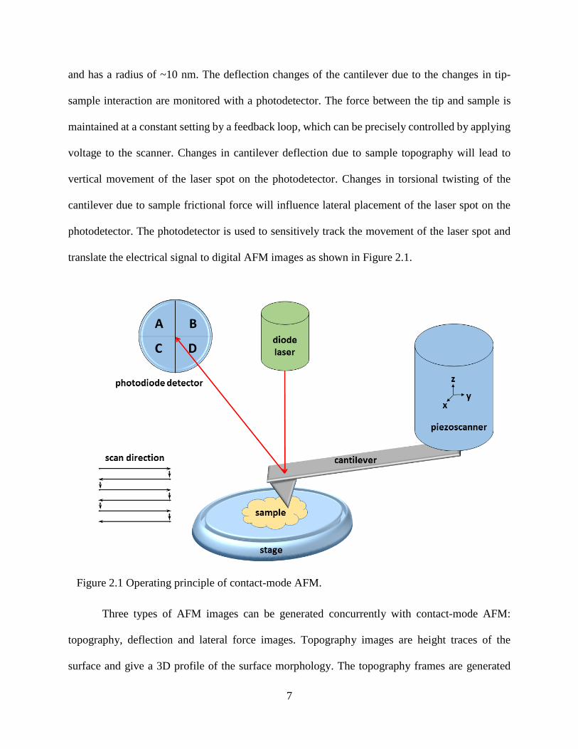
7
and has a radius of ~10 nm. The deflection changes of the cantilever due to the changes in tip-
sample interaction are monitored with a photodetector. The force between the tip and sample is
maintained at a constant setting by a feedback loop, which can be precisely controlled by applying
voltage to the scanner. Changes in cantilever deflection due to sample topography will lead to
vertical movement of the laser spot on the photodetector. Changes in torsional twisting of the
cantilever due to sample frictional force will influence lateral placement of the laser spot on the
photodetector. The photodetector is used to sensitively track the movement of the laser spot and
translate the electrical signal to digital AFM images as shown in Figure 2.1.
Three types of AFM images can be generated concurrently with contact-mode AFM:
topography, deflection and lateral force images. Topography images are height traces of the
surface and give a 3D profile of the surface morphology. The topography frames are generated
Figure 2.1 Operating principle of contact-mode AFM.
8
from plotting the scanner z piezo voltage adjustments of the feedback loop. Deflection images
show the error signal associated with the feedback loop. The deflection signal (error signal) is
small when parameters during imaging are optimized, therefore the deflection images are usually
not reported in the literature. As the tip is scanned across and interacts with the sample, frictional
force will cause lateral twisting of the tip. The lateral movement of the laser spot on the
photodetector is used to generate lateral force images. The lateral force images are used to
distinguish the differences in chemistry at the interface.
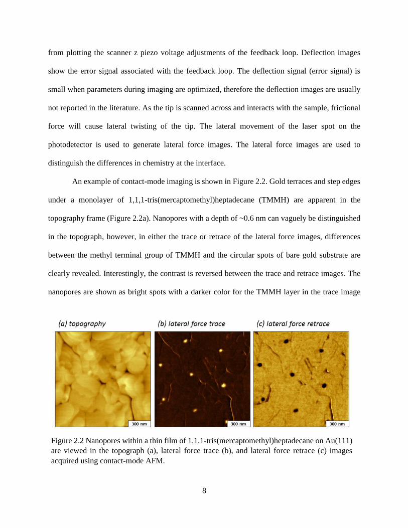
An example of contact-mode imaging is shown in Figure 2.2. Gold terraces and step edges
under a monolayer of 1,1,1-tris(mercaptomethyl)heptadecane (TMMH) are apparent in the
topography frame (Figure 2.2a). Nanopores with a depth of ~0.6 nm can vaguely be distinguished
in the topograph, however, in either the trace or retrace of the lateral force images, differences
between the methyl terminal group of TMMH and the circular spots of bare gold substrate are
clearly revealed. Interestingly, the contrast is reversed between the trace and retrace images. The
nanopores are shown as bright spots with a darker color for the TMMH layer in the trace image
Figure 2.2 Nanopores within a thin film of 1,1,1-tris(mercaptomethyl)heptadecane on Au(111)
are viewed in the topograph (a), lateral force trace (b), and lateral force retrace (c) images
acquired using contact-mode AFM.
9
(Figure 2.2b); whereas the nanopores are dark with brighter areas for TMMH in the retrace image
(Figure 2.2c). As the tip scans the surface in opposite directions the probe interacts with the surface
differently to produce a reversion in contrast between trace and retrace images of lateral force
channel.35
2.3 AFM Force Spectroscopy
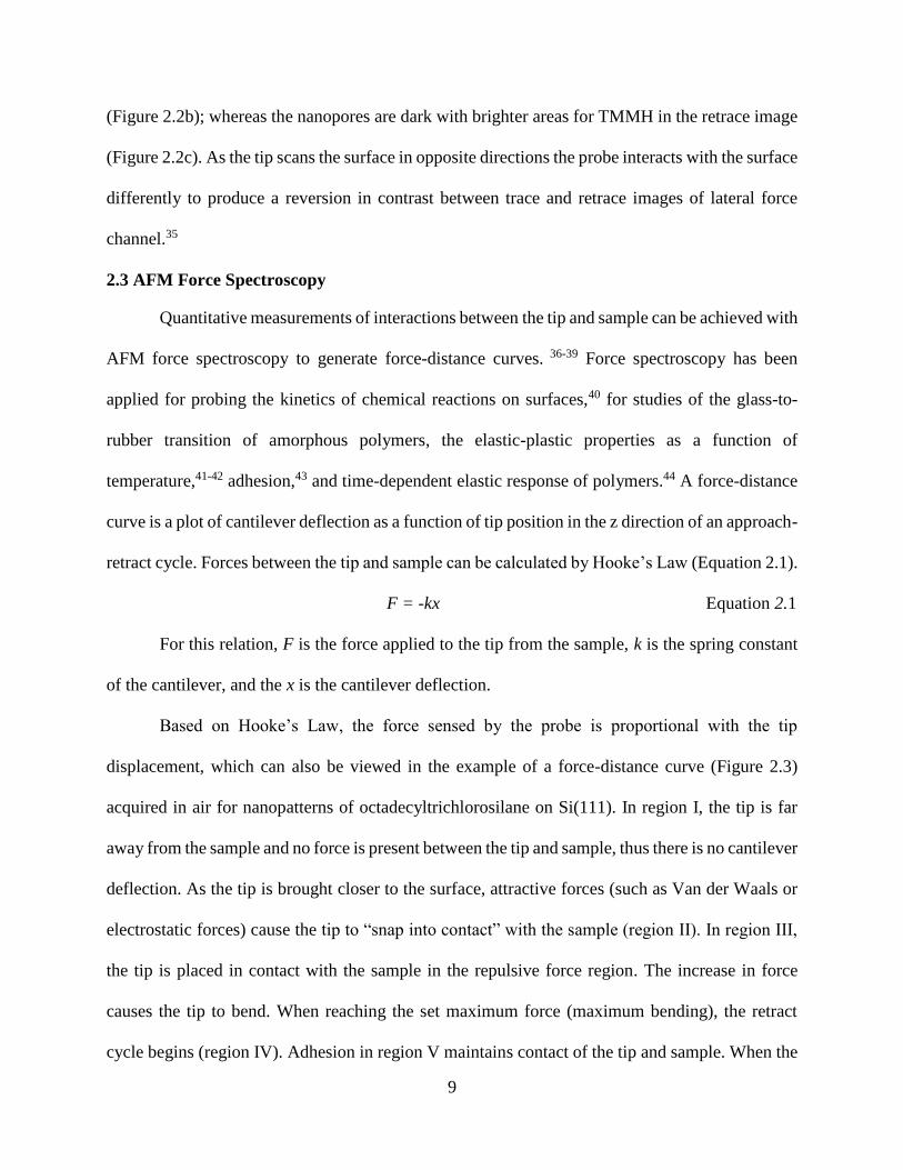
Quantitative measurements of interactions between the tip and sample can be achieved with
AFM force spectroscopy to generate force-distance curves. 36-39 Force spectroscopy has been
applied for probing the kinetics of chemical reactions on surfaces,40 for studies of the glass-to-
rubber transition of amorphous polymers, the elastic-plastic properties as a function of
temperature,41-42 adhesion,43 and time-dependent elastic response of polymers.44 A force-distance
curve is a plot of cantilever deflection as a function of tip position in the z direction of an approach-
retract cycle. Forces between the tip and sample can be calculated by Hooke’s Law (Equation 2.1).
F = -kx Equation 2.1
For this relation, F is the force applied to the tip from the sample, k is the spring constant
of the cantilever, and the x is the cantilever deflection.
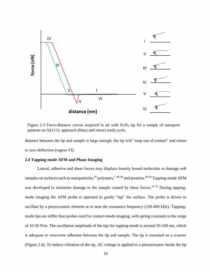
Based on Hooke’s Law, the force sensed by the probe is proportional with the tip
displacement, which can also be viewed in the example of a force-distance curve (Figure 2.3)
acquired in air for nanopatterns of octadecyltrichlorosilane on Si(111). In region I, the tip is far
away from the sample and no force is present between the tip and sample, thus there is no cantilever
deflection. As the tip is brought closer to the surface, attractive forces (such as Van der Waals or
electrostatic forces) cause the tip to “snap into contact” with the sample (region II). In region III,
the tip is placed in contact with the sample in the repulsive force region. The increase in force
causes the tip to bend. When reaching the set maximum force (maximum bending), the retract
cycle begins (region IV). Adhesion in region V maintains contact of the tip and sample. When the
10
distance between the tip and sample is large enough, the tip will “snap out of contact” and return
to zero deflection (region VI).
2.4 Tapping-mode AFM and Phase Imaging
Lateral, adhesive and shear forces may displace loosely bound molecules or damage soft
samples on surfaces such as nanoparticles,45 polymers,7, 46-48 and proteins.49-50 Tapping-mode AFM
was developed to minimize damage to the sample caused by shear forces.51-53 During tapping-
mode imaging the AFM probe is operated to gently “tap” the surface. The probe is driven to
oscillate by a piezoceramic element at or near the resonance frequency (150-400 kHz). Tapping-
mode tips are stiffer than probes used for contact-mode imaging, with spring constants in the range
of 10-50 N/m. The oscillation amplitude of the tips for tapping-mode is around 50-100 nm, which
is adequate to overcome adhesion between the tip and sample. The tip is mounted on a scanner
(Figure 2.4). To induce vibration of the tip, AC voltage is applied to a piezoactuator inside the tip
Figure 2.3 Force-distance curves acquired in air with Si3N4 tip for a sample of nanopore
patterns on Si(111): approach (blue) and retract (red) cycle.
11
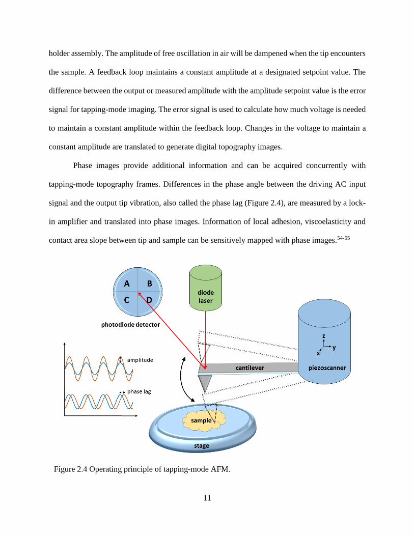
holder assembly. The amplitude of free oscillation in air will be dampened when the tip encounters
the sample. A feedback loop maintains a constant amplitude at a designated setpoint value. The
difference between the output or measured amplitude with the amplitude setpoint value is the error
signal for tapping-mode imaging. The error signal is used to calculate how much voltage is needed
to maintain a constant amplitude within the feedback loop. Changes in the voltage to maintain a
constant amplitude are translated to generate digital topography images.
Phase images provide additional information and can be acquired concurrently with
tapping-mode topography frames. Differences in the phase angle between the driving AC input
signal and the output tip vibration, also called the phase lag (Figure 2.4), are measured by a lock-
in amplifier and translated into phase images. Information of local adhesion, viscoelasticity and
contact area slope between tip and sample can be sensitively mapped with phase images.54-55
Figure 2.4 Operating principle of tapping-mode AFM.

12
An example of tapping-mode topography and phase images is shown in Figure 2.5 for a
sample of patterned nanorings of N-(6-aminohexyl)aminopropyltrimethoxysilane prepared using
particle lithography with chemical vapor deposition.56 The surface morphology and a height profile
of the nanoring sample are presented in the topography channel, where brighter contrast indicates
the taller structures on surface (surface z scale: 5.7 nm). The difference in color contrast among
the ring, the center areas of the ring, and the surrounding matrix areas shown in the phase images
indicate changes in elastic response for different regions of the sample. The small particles between
the rings can be clearly resolved in the phase image.
Tapping-mode is particularly suitable for polymer samples which have viscoelastic
properties. Phase images can elucidate fine details of the sample that topography cannot provide,
especially for phase separated system such as polymer blends of polystyrene and polybutadiene,57
lamellae structure of block copolymer polystyrene-b-polymethylmethacrylate,58 and segmented
Figure 2.5 Nanorings of N-(6-aminohexyl)aminopropyltrimethoxysilane imaged with tapping-
mode AFM. (a) Topography and (b) phase images.
13
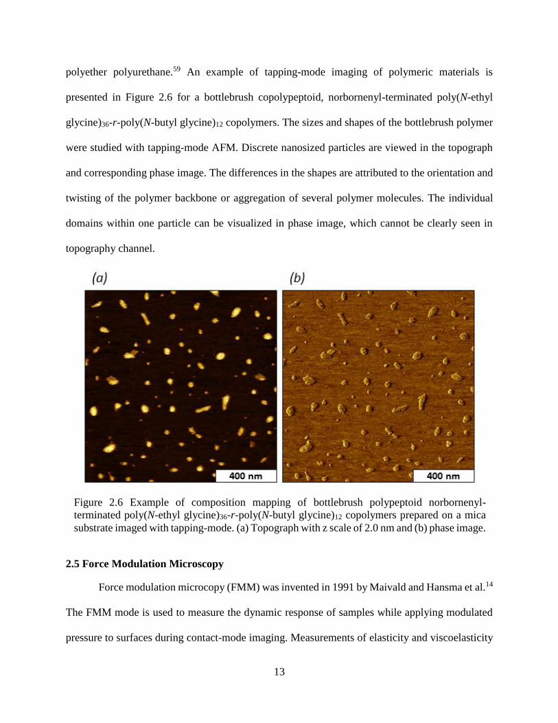
polyether polyurethane.59 An example of tapping-mode imaging of polymeric materials is
presented in Figure 2.6 for a bottlebrush copolypeptoid, norbornenyl-terminated poly(N-ethyl
glycine)36-r-poly(N-butyl glycine)12 copolymers. The sizes and shapes of the bottlebrush polymer
were studied with tapping-mode AFM. Discrete nanosized particles are viewed in the topograph
and corresponding phase image. The differences in the shapes are attributed to the orientation and
twisting of the polymer backbone or aggregation of several polymer molecules. The individual
domains within one particle can be visualized in phase image, which cannot be clearly seen in
topography channel.
2.5 Force Modulation Microscopy
Force modulation microcopy (FMM) was invented in 1991 by Maivald and Hansma et al.14
The FMM mode is used to measure the dynamic response of samples while applying modulated
pressure to surfaces during contact-mode imaging. Measurements of elasticity and viscoelasticity
Figure 2.6 Example of composition mapping of bottlebrush polypeptoid norbornenyl-
terminated poly(N-ethyl glycine)36-r-poly(N-butyl glycine)12 copolymers prepared on a mica
substrate imaged with tapping-mode. (a) Topograph with z scale of 2.0 nm and (b) phase image.
14
can be acquired with FMM. Materials that have been studied with FMM include patterned self-
assembled monolayers (SAMs),60 polymer blends and resins,61-64 protein-lipid aggregates,65 wood
cells and fibroblasts,66-68 bacteria,69 porous silicon,70 as well as optical thin film materials.71
Quantitative measurements such as Young’s modulus72-74 and the elasticity75-76 of samples can be
evaluated using FMM.
For force modulation microscopy, the tip is operated in contact-mode, which means the tip
is operated in continuous contact with the surface during scanning. Either the sample or tip is
driven to vibrate with pressure applied at the area of tip-sample contact. Most commonly FMM
has been done using an instrument configuration with the sample placed directly on top of an xyz
scanner and actuation of the z piezoelement causes the sample to vibrate for tip displacements of
a few nm in the z-direction.62, 77-82 For a scan-by-tip AFM configuration, an FMM sample stage
was invented by our group in collaboration with Dr. Song Xu and Sonimoto Laboratory to facilitate
FMM measurements. Machined polycarbonate was used to construct the sample stage. Current
can be applied through a coxial cable connection to the piezoactuator within the stage to generate
z axis vibration. Details of the FMM sample stage will be presented in Chapter 6.
Other than stage-driven FMM, tip-vibration FMM has been developed and applied. For
example, a cantilever holder equipped with bimorph piezoelements was used to accomplish force
modulation, which can actuate the tip as it is pressed against the sample.63, 83-84 A magnetic field
has been used to drive the vibration of a tip or tip-holder assembly to accomplish force modulation
imaging.76, 85-88 One way to use magnetically actuated system, named indirect magnetic
modulation (IMM), was introduced by our group.86 For IMM, an AC current is applied to a MAC
mode sample stage and an electromagnetic field is generated from a solenoid underneath the MAC
stage. A tip-holder assembly or nosecone containing ferromagnetic material is induced to vibrate
15
with the flux of the electromagnetic field. The AFM is operated in contact-mode, therefore,
information of height, elasticity and adhesion are simultaneously acquired. The vibration
frequency and amplitude can be tuned to obtain the highly sensitive images.89 Comparison of FMM
using the newly designed sample stage and IMM will be presented in Chapter 7.
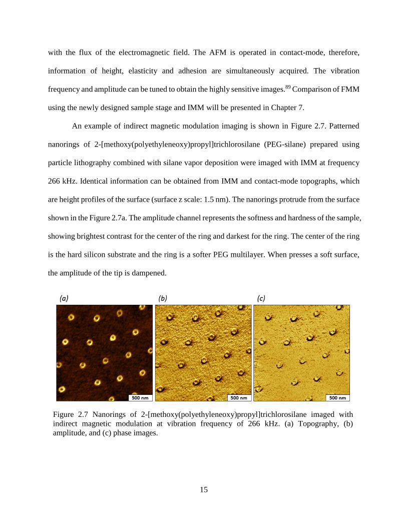
An example of indirect magnetic modulation imaging is shown in Figure 2.7. Patterned
nanorings of 2-[methoxy(polyethyleneoxy)propyl]trichlorosilane (PEG-silane) prepared using
particle lithography combined with silane vapor deposition were imaged with IMM at frequency
266 kHz. Identical information can be obtained from IMM and contact-mode topographs, which
are height profiles of the surface (surface z scale: 1.5 nm). The nanorings protrude from the surface
shown in the Figure 2.7a. The amplitude channel represents the softness and hardness of the sample,
showing brightest contrast for the center of the ring and darkest for the ring. The center of the ring
is the hard silicon substrate and the ring is a softer PEG multilayer. When presses a soft surface,
the amplitude of the tip is dampened.
Figure 2.7 Nanorings of 2-[methoxy(polyethyleneoxy)propyl]trichlorosilane imaged with
indirect magnetic modulation at vibration frequency of 266 kHz. (a) Topography, (b)
amplitude, and (c) phase images.
16
2.6 In Situ Temperature Studies Using AFM
Dynamic studies with time-lapse AFM experiments using a heating stage have been
reported.90 The crystallization and melting of poly(ethylene oxides) and polyethylene,91-92 the
crystal-mesophase transition of poly(di-n-hexylsilane) and poly(di-n-butylsilane),93 the phase
transition behavior of single thermo-responsive hydrogel particles: poly(N-isopropylacrylamide-
co-acrylic acid),94 the phase transition of a nanocomposite,86 and diblock copolymer domains in
directed self-assembly have been investigated in situ using AFM.
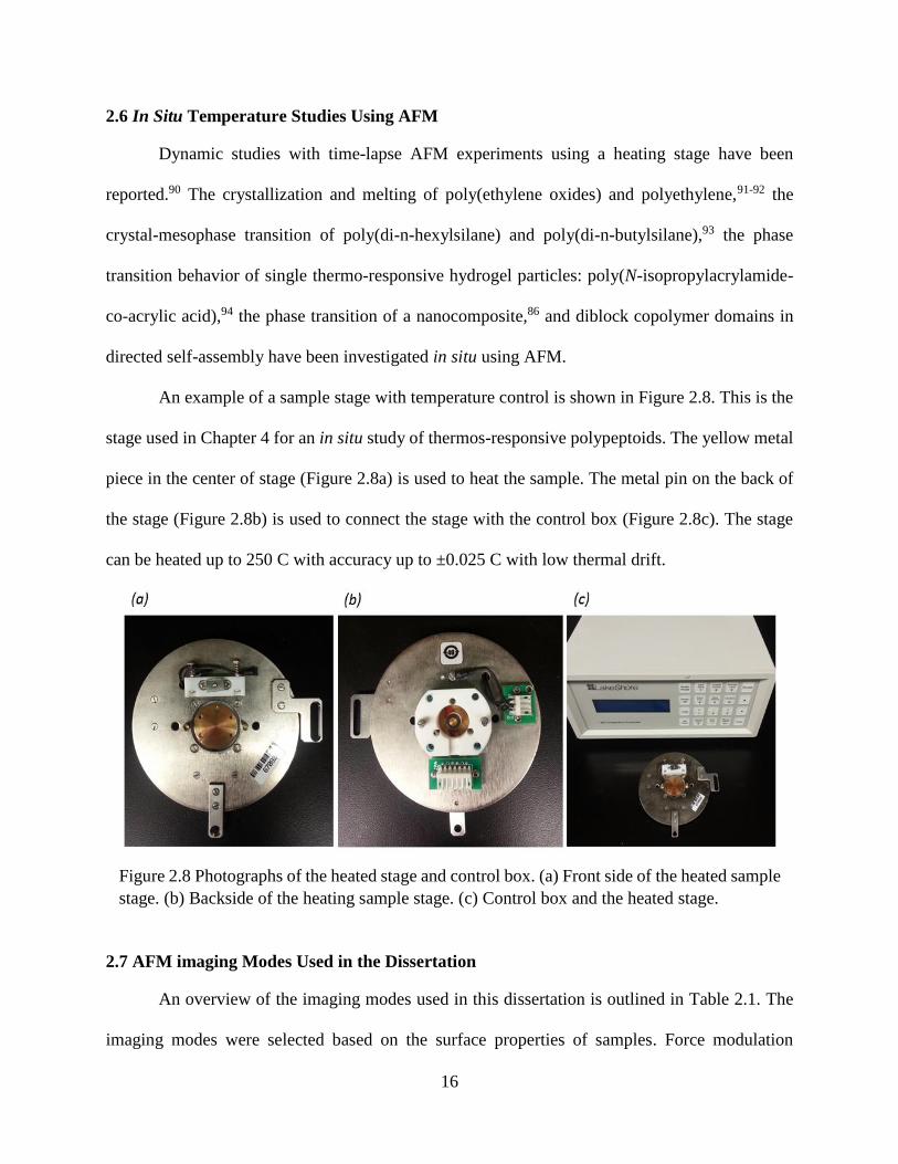
An example of a sample stage with temperature control is shown in Figure 2.8. This is the
stage used in Chapter 4 for an in situ study of thermos-responsive polypeptoids. The yellow metal
piece in the center of stage (Figure 2.8a) is used to heat the sample. The metal pin on the back of
the stage (Figure 2.8b) is used to connect the stage with the control box (Figure 2.8c). The stage
can be heated up to 250 C with accuracy up to ±0.025 C with low thermal drift.
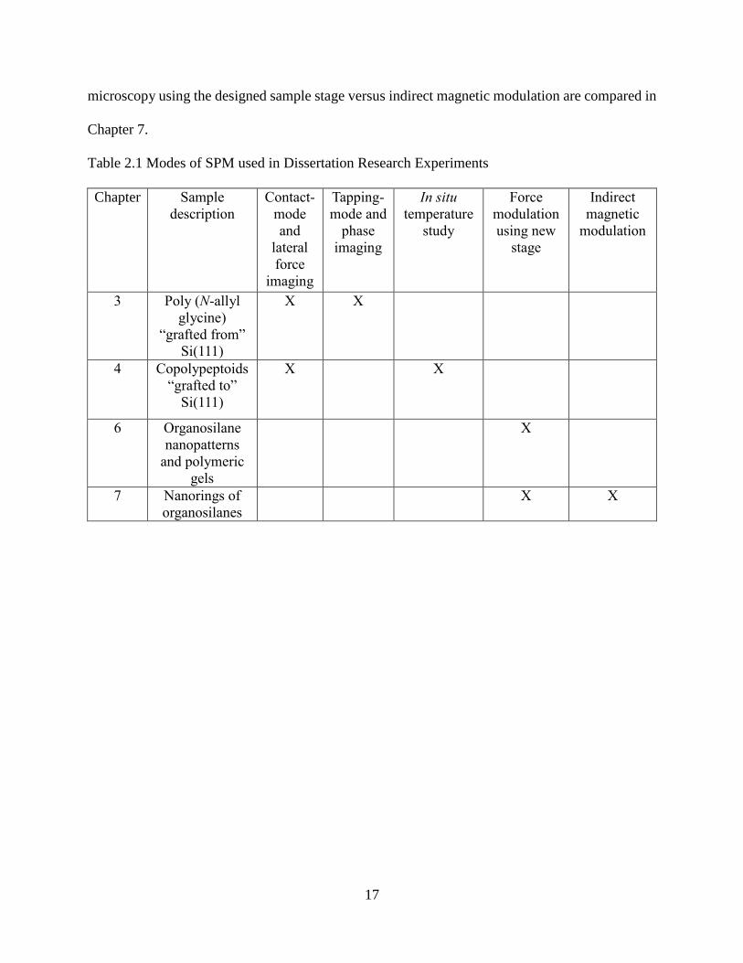
2.7 AFM imaging Modes Used in the Dissertation
An overview of the imaging modes used in this dissertation is outlined in Table 2.1. The
imaging modes were selected based on the surface properties of samples. Force modulation
Figure 2.8 Photographs of the heated stage and control box. (a) Front side of the heated sample
stage. (b) Backside of the heating sample stage. (c) Control box and the heated stage.
17
microscopy using the designed sample stage versus indirect magnetic modulation are compared in
Chapter 7.
Table 2.1 Modes of SPM used in Dissertation Research Experiments
Chapter Sample
description
Contact-
mode
and
lateral
force
imaging
Tapping-
mode and
phase
imaging
In situ
temperature
study
Force
modulation
using new
stage
Indirect
magnetic
modulation
3 Poly (N-allyl
glycine)
“grafted from”
Si(111)
X X
4 Copolypeptoids
“grafted to”
Si(111)
X X
6 Organosilane
nanopatterns
and polymeric
gels
X
7 Nanorings of
organosilanes
X X
18
CHAPTER 3. DIRECTED GROWTH OF POLYMER NANOPILLARS USING
SURFACE-INITIATED RING-OPENING POLYMERIZATION OF N-ALLYL N-
CARBOXYANHYDRIDE
3.1 Introduction
Peptide-functionalized thin films have been applied as stimuli responsive materials,95 anti-
fouling agents96-97 and as inorganic/peptide hybrids.98 Poly(α-peptoid)s, a class of pseudo-peptidic
polymers, feature a polyglycine backbone with substitution on the nitrogen atoms.99-100 The
biocompatibility, backbone degradability and processability of poly(α-peptoid)s make these
polymers useful for applications such as smart coatings, biosensors and bioseparations.99 There
are relatively few publications reporting studies of polypeptoid thin films101 or reports focusing on
nanopatterns of polypeptoid brushes on surfaces. Surface structures of peptides have previously
been reported to accomplish micron-scale patterning using photolithography102-103 and micro-
contact printing.104-105 We report results for combining particle lithography with surface-initiated
ring-opening polymerization of N-allyl N-carboxyanhydride (allyl-NCA) to prepare polymer
pillars of poly(N-allyl glycine).
To prepare polypeptide/peptoid brushes, there are two commonly used methods, “graft to”
and “graft from”.106-107 The “graft to” approach involves a reaction between surface reactive
moieties and the end-groups of pre-synthesized polypeptide/peptoid. The method is
experimentally simple however it is difficult to achieve high grafting densities because of the steric
crowding. The “graft from” method, also known as the “surface-initiated” approach, occurs
through a ring-opening polymerization of α-amino acid N-carboxyanhydride (NCAs) with
initiators attached to surfaces. Control of the functionality, density and thickness of polymer
nanopillars with molecular precision using the “graft from” approach can be readily achieved.106
Amine-functionalized substrates in either solution or vapor phase were used to prepare thin
films of polypeptide brushes using surface-initiated polymerization (the “graft from” method).108-

19
114 The “graft from” and “graft to” approaches for grafting poly (γ-benzyl-L-glutamate) (PBLG)
film on silicon oxide surface was reported in 1996.109 To obtain better control of PBLG film
thickness, a protocol with vapor deposition polymerization was developed which involved a
reaction between the vapor species of γ-benzyl-L-glutamate and a primary amine modified silicon
substrate.110 The vapor deposition method was improved so that the α-helical PBLG films were
fabricated in less than 1 h with tunable thickness from a few nanometers to hundreds of
nanometers.115 Mechanistic studies of surface-initiated vapor deposition polymerization of PBLG
were reported by Zheng et al.116 The helix orientation of PBLG and poly(γ-methyl L-glutamate)
(PMLG) were studied using FT-IR transmission spectroscopy.117-119 The surface-grafting of AB-
block copolypeptides, PBLG-b-PMLG, was also introduced.119 Synthesis of surface-tethered
poly(L-glutamic acid) (PLGA) and poly(L-lysine) (PLL) and the conformational transition (α-
helix, β-sheet, and random coil) for the responsiveness to the external stimuli of pH, surfactant and
ions were investigated using circular dichroism (CD).120-122 Well-defined homo- and block-
polypeptides were prepared by transition metal-mediated polymerization of NCAs, demonstrated
by Deming et al.123-125 Polystyrene particles functionalized with PBLG were obtained by ring-
opening polymerization of NCAs by nickel amido-amidate complexes.126 Thiol-clickable and
block copolypeptide brushes were synthesized via a nickel-mediated surface-initiated
polymerization resulting in an effective approach to functionalize polypeptide surfaces.107
Particle lithography, is a facile and versatile fabrication technique applicable for generating
nanostructures with regular nanoscale geometries with high reproducibility.127 Solutions of
monodisperse mesospheres self-assemble into close-packed arrangements on surfaces during
evaporation of solvents. The periodic mask that is formed on surfaces can be used for nano- or
micron- scale fabrication.127-131 The advantages of particle lithography include the generic use of
20
basic lab equipment and experimental steps, and the capability for tuning the dimensions of surface
structures according to the diameters of mesospheres.128
Using particle lithography, porous polymer films were prepared using materials, such as
polycaprolactone,132 poly(N-isopropylacrylamide),133 polyethersulfone,134-135 and
polythiophene.136-137 The first surface-initiated and site-specific Suzuki polycondensation to
quickly and selectively graft polyfluorene from functionalized, sub-micron surface patterns at
room temperature was developed by Beryozkina et al.138 A range of robust and simple patterning
strategies using microsphere arrays as a surface mask were combined with surface-initiated atom
transfer radical polymerization to fabricate patterned triangular, ring-shaped, dot-like, or hole-like
poly(N-isopropylacrylamide) brush microstructures.139-140 Surface-imprinted polymer films for
protein recognition were prepared by immobilizing avidin on monodisperse polystyrene beads,
then depositing the beads onto gold-coated quartz crystal, followed by electropolymerization of
3,4-ethylenedioxythiophene and finally dissolving away the beads.141 A binary compositionally
patterned surface containing poly(carbazole) and poly(N-isopropylacrylamide) was prepared via
colloidal-template assisted electropolymerization followed by growing the polymer brushes using
SI-ATRP.142
Particle lithography and organosilane chemistry were used to prepare nanopores within a
thin film of octadecyltrichlorosilane (OTS).143-144 Uncovered sites of Si(111) were backfilled with
(3-aminopropyl)triethoxysilane (APTES) as a means to direct the growth of N-allyl N-
carboxyanhydride (allyl-NCA).145 Each step during the preparation of the surface platform was
characterized by atomic force microscopy (AFM), which has been previously used for studying
surface-grafted polymer nanopillars.146-151 The polypeptoid nanopillars have reactive side chains,
since allyl-NCA with a pendent allyl group was chosen as the monomer. The polymer can be
21
further functionalized by thiol-ene click reaction for constructing complex surface structures.152-
154
3.2 Experimental Section
3.2.1 Materials and Reagents
Reagents were used as received without further purification. Octadecyltrichlorosilane
(OTS) was purchased from Gelest (Morrisville, PA). Anhydrous toluene, bicyclohexyl, (3-
Aminopropyl)triethoxysilane (APTES), dichloroacetic acid, chloroform, sulfuric acid (ACS
reagent 95%) and hydrogen peroxide (30%) were obtained from Sigma-Aldrich. Pieces of single-
sided polished Si(111) doped with boron (Ted Pella, Inc., Redding, CA) were used as substrates.
Monodisperse silica mesospheres with diameter 0.49 ± 0.02 μm were acquired from Duke, Inc.
(Fremont, CA). The deionized water used for experiments was from a Direct-Q3 system (18 MΩ,
Millipore, Bedford, MA).
3.2.2 Atomic Force Microscopy
Samples were characterized using either a model 5500 or 5420 atomic force microscope
(Agilent Technologies, Chandler, AZ). Nonconductive V-shaped cantilevers made of silicon
nitride with force constants ranging from 0.01-0.60 N/m were used for contact-mode imaging
(Bruker Probes, Camarillo, CA). Silicon nitride cantilevers with an average force constant of 48
N/m and a resonance frequency of 190 kHz were used for tapping-mode imaging (Vista probes,
Phoenix, AZ). Images were processed using Gwyddion open source software which is supported
by the Czech Metrology Institute.155
3.2.3 Preparation of Nanopores within an OTS Film
Particle lithography was used to generate organosilane nanopore patterns on Si(111)
surfaces.143 The silicon substrates were cleaned by immersion in piranha solution for 2 h. Piranha
solution, which is a mixture of sulfuric acid and hydrogen peroxide at a ratio of 3:1 (v/v), is highly
22
corrosive and should be handled cautiously. Substrates were rinsed copiously with deionized water
and dried under argon. Monodisperse silica mesospheres were washed three times by
centrifugation to remove trace charge stabilizers or surfactants. The pellet of silica mesospheres
was resuspended in water by vortex mixing, and a drop (10 μL) was deposited on a clean substrate.
The sample was dried in air for 2 h to produce surface masks for further chemical steps. As water
evaporated during the drying step, capillary forces pull the mesospheres together to form
crystalline layers on flat surface. Next, the substrate was placed in an oven at 140 C for 24 h to
temporarily anneal the mesospheres to the surface. After cooling, the sample was immersed in a
0.1% solution of OTS (v/v) in toluene for 5 h. Next the sample was rinsed with water and ethanol.
To remove the mesoparticles, the substrate was sonicated for 15 min in ethanol and water
successively. The sample was dried under argon for AFM characterization.
3.2.4 Preparation of APTES Nanodots
The substrate (polished Si wafer) with OTS nanopores was cleaned by sonication in ethanol
for 10 min to remove contaminants, then dried under argon. Uncovered bare areas of the Si
substrates were backfilled with initiator by immersion in an APTES solution (0.02% v/v solution
of APTES in bicyclohexyl for 3 h). Next, the samples were rinsed with acetone, water and ethanol,
followed by 15 min sonication in ethanol and in water. The samples were dried under argon and
characterized with AFM.
3.2.5 Three Steps Synthesis of Allyl-NCA
Synthesis of 2-(Allylamino)acetic Acid Hydro-chloride: Allylamine (15 mL, 0.2 mol) and
glycoxylic acid (30 g, 0.4 mol) were both dissolved in CH2Cl2 and stirred at room temperature for
a period of 24 h. The solvent was removed and 1 N HCl aqueous solution (300 mL) was added to
the flask (Scheme 3.1). The mixture was refluxed overnight at 110 C. The solvent was evaporated
to yield brown viscous oil. Recrystallization in cold methanol and THF afforded white crystals
23
(11.53 g, 38% yield). 1H NMR (δ in MeOD, ppm): 5.7 (m, =CH-); 5.3 (t, =CH2); 3.7 (s, -CH2-);
3.5 (d, =CHCH2-). 13C{1H} NMR (δ in CDCl3, ppm) 166.3 (C=O); 129.8 (-CH=CH2); 121.0 (-
CH=CH2); 48.9 (-CH2-); 46.4 (-CH2-).
2-(Allyl(tert-butoxycarbonyl)amino)acetic Acid (2): 1 (11.53 g, 0.076 mol) and di-tert
butoxide (41.40 g, 0.191 mol) were dissolved in distilled water (250 mL). The solution was stirred,
and then triethylamine (53.10 mL, 0.382 mol) was added via syringe. The reaction was stirred
overnight at room temperature. The solution was washed with hexanes to remove excess di-tert-
butoxide (100 mL) and then the aqueous portion was made acidic using 1N HCl (roughly 150 mL).
The aqueous portion was washed twice with ethyl acetate (100 mL) then the combined organic
layers were washed once with brine (70 mL). The organic layer was dried with MgSO4, filtered
and then the solvent was removed under vacuum to yield a pale yellow oil (16.2 g, 0.075 mol, 99%
yield). 1H NMR (δ in CDCl3, ppm): 10.4 (bs, -OH); 5.7 (m, =CH-); 5.3 (t, =CH2); 3.7 (s, -CH2-);
3.5 (d, =CHCH2-); 1.4 (s, -(CH3)3). 13C{1H} NMR (δ in CDCl3, ppm): 173.4 (-NCOO-); 167.1 (-
COOH); 131.1 (-CH=CH2); 119.9 (-CH=CH2); 78.9 (C(CH3)3); 49.8 (-CH2N-); 47.6 (-CH2CH=);
28.1 (-(CH3)3).
Scheme 3.1 Synthetic procedure for allyl-NCA
24
Synthesis of Allyl-NCA (3): 2 (16.2 g, 0.075 mol) was dissolved in anhydrous
dichloromethane and while under an argon atmosphere, the solution was chilled to 0 C. PCl3 (7.5
mL, 0.086 mol) was added to the solution via syringe. The solution was stirred at 0 C for one hour,
after which the solution was kept at 25 C for 2 h. The solvent was then removed under vacuum and
the flask was placed into a glove box. The residue was redissolved in anhydrous dichloromethane,
and stirred with NaH for 10 min. The solution was filtered and the filtrate was concentrated,
leaving clear oil. The oil was vacuum distilled at 60 C in the modified vacuum distillation apparatus.
The final product was a clear liquid (5.94 g, 0.042 mol, 54%). 1H NMR (δ in Tol-d8, ppm): 5.2
(m, =CH); 4.8 (m, =CH2); 3.4 (d, -CH2-); 2.9 (s, =CHCH2-). 13C{1H}c NMR (δ in Tol-d8, ppm):
160.3 (-CH2C(O)O); 147.0 (-OC(O)N-); 132.1 (-CH=CH2); 113.7 (CH2=CH-); 42.4 (=CHCH2N-);
40.3 (C(O)CH2N-).
3.2.6 Polymerization of Allyl-NCA.
Substrates with OTS and APTES nanopatterns were immersed for 24 h in 0.43 M allyl-
NCA solution in THF at 50 C under N2. Afterward, the substrates were rinsed with THF and then
immersed for 2 days in a mixture of dichloroacetic acid and chloroform at a 1:4 (v/v) ratio to
remove physically adsorbed molecules, followed by rinsing with chloroform, water and ethanol.
The sample was then dried under argon.117
3.3 Results and Discussion
The strategy for spatially directing the polymerization of allyl-NCA is outlined in Figure
3.1. A close-packed arrangement of silica mesospheres on Si(111) served as a surface mask for
defining the sites for depositing of OTS (Figure 3.1a). A masked substrate was immersed in a
solution of OTS to enable molecules to self-assemble on areas of exposed Si surrounding the
mesospheres (Figure 3.1b). Nanopores within the OTS thin film were produced after removal of
silica mesospheres (Figure 3.1c). The initiator (APTES) was selectively grown inside the OTS
25
nanopores to form a chemically patterned surface (Figure 3.1d). The nanodots of APTES provided
sites for spatially selective growth of polymer. Surface-initiated ring-opening polymerization of
allyl-NCA took place at sites where the primary amine (APTES) was located (Figure 3.1e).
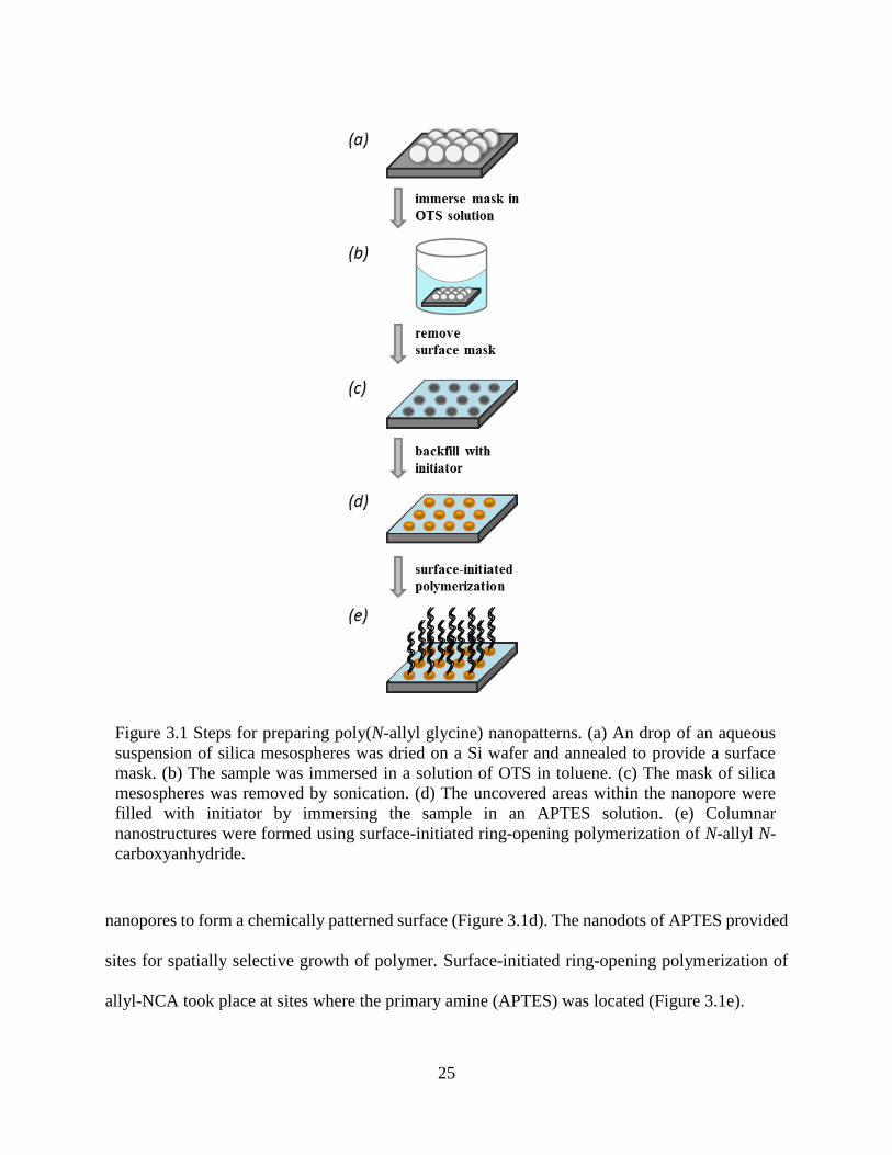
Figure 3.1 Steps for preparing poly(N-allyl glycine) nanopatterns. (a) An drop of an aqueous
suspension of silica mesospheres was dried on a Si wafer and annealed to provide a surface
mask. (b) The sample was immersed in a solution of OTS in toluene. (c) The mask of silica
mesospheres was removed by sonication. (d) The uncovered areas within the nanopore were
filled with initiator by immersing the sample in an APTES solution. (e) Columnar
nanostructures were formed using surface-initiated ring-opening polymerization of N-allyl N-
carboxyanhydride.
26
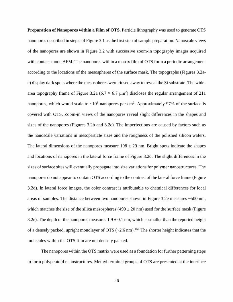
Preparation of Nanopores within a Film of OTS. Particle lithography was used to generate OTS
nanopores described in step c of Figure 3.1 as the first step of sample preparation. Nanoscale views
of the nanopores are shown in Figure 3.2 with successive zoom-in topography images acquired
with contact-mode AFM. The nanopores within a matrix film of OTS form a periodic arrangement
according to the locations of the mesospheres of the surface mask. The topographs (Figures 3.2a-
c) display dark spots where the mesospheres were rinsed away to reveal the Si substrate. The wide-
area topography frame of Figure 3.2a (6.7 × 6.7 μm2) discloses the regular arrangement of 211
nanopores, which would scale to ~109 nanopores per cm2. Approximately 97% of the surface is
covered with OTS. Zoom-in views of the nanopores reveal slight differences in the shapes and
sizes of the nanopores (Figures 3.2b and 3.2c). The imperfections are caused by factors such as
the nanoscale variations in mesoparticle sizes and the roughness of the polished silicon wafers.
The lateral dimensions of the nanopores measure 108 ± 29 nm. Bright spots indicate the shapes
and locations of nanopores in the lateral force frame of Figure 3.2d. The slight differences in the
sizes of surface sites will eventually propagate into size variations for polymer nanostructures. The
nanopores do not appear to contain OTS according to the contrast of the lateral force frame (Figure
3.2d). In lateral force images, the color contrast is attributable to chemical differences for local
areas of samples. The distance between two nanopores shown in Figure 3.2e measures ~500 nm,
which matches the size of the silica mesospheres (490 ± 20 nm) used for the surface mask (Figure
3.2e). The depth of the nanopores measures 1.9 ± 0.1 nm, which is smaller than the reported height
of a densely packed, upright monolayer of OTS (~2.6 nm).156 The shorter height indicates that the
molecules within the OTS film are not densely packed.
The nanopores within the OTS matrix were used as a foundation for further patterning steps
to form polypeptoid nanostructures. Methyl terminal groups of OTS are presented at the interface
27
to furnish a resist layer that does not react with allyl-NCA for patterning of polypeptoid. The
nanoscopic bare areas of the Si substrate within the nanopores provide hydroxyl groups to spatially
define sites where amino-silane molecules will bind to grow polymer nanostructures.
Figure 3.2 Nanopores within a film of OTS prepared using 500 nm silica mesospheres. (a)
Contact-mode AFM topography image of nanopatterns prepared on Si(111). (b) Zoom-in view.
(c) Magnified view of nanopores and (d) simultaneously acquired lateral force image. (e)
Cursor profile for the line in c.
28
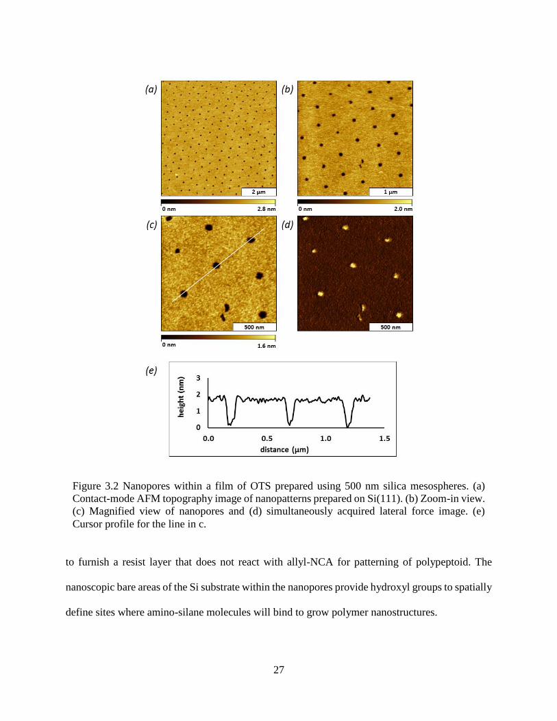
Selective Filling of APTES Initiator into Nanopores. The initiator (APTES) molecules
assembled into the uncovered areas of the Si substrate within OTS to form regular nanodot patterns,
as shown in Figure 3.3. The bright spots are backfilled APTES nanodots and the darker areas in
the background are the OTS matrix (topography frame, Figure 3.3a). The hexagonal arrangement
Figure 3.3 After selective filling of the nanopores with APTES, surface views with contact-
mode AFM. (a) The nanodots of APTES are taller than the surrounding OTS resist in the
topography images, 6.7 × 6.7 μm2; (b) zoom-in topograph; (c) close-up view of eight nanodots
with (d) corresponding lateral force image. (e) Height profile for three nanodots indicated in c.
29
of APTES nanodots are apparent in Figures 3.3b and 3.3c. There are 38 nanodots in Figure 3.3b,
which accordingly scales to ~109 nanodots per cm2. The results indicate that OTS is an excellent
resist since the growth of APTES was confined to areas inside the nanopores. The surface contains
chemical patterns of methyl and amine terminal groups for further steps of site selective polymer
growth. The differences in surface chemistry are distinctly apparent in the high-resolution lateral
force image of Figure 3.3d. The height of the nanodots measured 10 ± 1.2 nm (including the depth
of the nanopores), which corresponds to multilayers of APTES. The height of three selected
APTES nanodots are shown in Figure 3.3e as an example measurement. The lateral dimension of
the APTES nanodots measured 110 ± 25 nm, which matches the dimensions of the unfilled
nanopores.
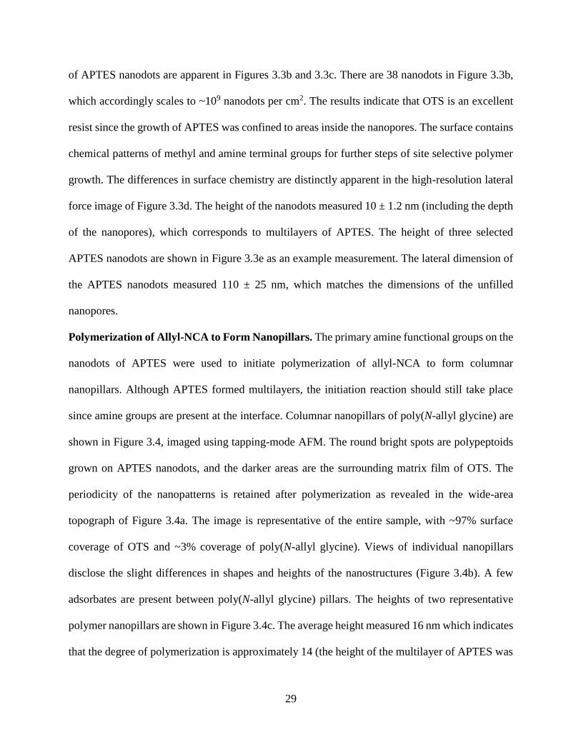
Polymerization of Allyl-NCA to Form Nanopillars. The primary amine functional groups on the
nanodots of APTES were used to initiate polymerization of allyl-NCA to form columnar
nanopillars. Although APTES formed multilayers, the initiation reaction should still take place
since amine groups are present at the interface. Columnar nanopillars of poly(N-allyl glycine) are
shown in Figure 3.4, imaged using tapping-mode AFM. The round bright spots are polypeptoids
grown on APTES nanodots, and the darker areas are the surrounding matrix film of OTS. The
periodicity of the nanopatterns is retained after polymerization as revealed in the wide-area
topograph of Figure 3.4a. The image is representative of the entire sample, with ~97% surface
coverage of OTS and ~3% coverage of poly(N-allyl glycine). Views of individual nanopillars
disclose the slight differences in shapes and heights of the nanostructures (Figure 3.4b). A few
adsorbates are present between poly(N-allyl glycine) pillars. The heights of two representative
polymer nanopillars are shown in Figure 3.4c. The average height measured 16 nm which indicates
that the degree of polymerization is approximately 14 (the height of the multilayer of APTES was
30
removed from the calculation). The tallest nanostructure is 35 nm, which shows the highest degree
of polymerization assuming that the polymer backbone is fully stretched (~62). The shortest
nanostructure is 10 nm, which is the same height as the APTES nanodots indicating that no
polymerization took place at some sites (10% of the polymer nanodots). The lateral dimension of
the polypeptoids measured 110 ± 13 nm, which closely matches the lateral dimensions of APTES
nanodots. The heights suggest that poly(N-allyl glycine) growth is predominantly in the z direction,
Figure 3.4 Surface-initiated ring-opening polymerization of N-allyl N-carboxyanhydride on
sites with APTES nanodots. (a) Nanostructures are taller after steps of polymerization, shown
in the topographs; (b) zoom-in view of polypeptoid pillars; (e) Cursor profile for two
nanopillars in a.
31
rather than growth of wider nanostructures. The distance between two polymer nanopillars
measured ~500 nm, corresponding to the expected dimensions of the silica mask.
The APTES initiated ring-opening polymerization of allyl-NCA in solution is a living
polymerization. When polymerization occurs on the surface, the reactivity of molecules is spatially
restricted. Since the sizes of the nanopores are slightly different, the number of APTES molecules
within a single nanopore varies, which influences the chain lengths of poly(N-allyl glycine). With
increase of the nanopore size, the heights of the polymer nanopillars correspondingly increased.
However the growth did not correspond to a linear relation. The drawback of using the “graft from”
method leads to an increased difficulty in controlling both the initiation and propagation steps.
Three Key Steps of Preparing Patterned Poly(N-allyl glycine). The key steps to prepare
patterned polymer nanopillars are shown in Figure 3.5. Nanopores within a film of OTS were
prepared using particle lithography combined with silane immersion (Figure 3.5a). The APTES
initiator was backfilled into exposed sites of OTS nanopores and formed nanodots (Figure 3.5b).
Polymerization of allyl-NCA occurred selectively at sites where APTES nanodots were located
(Figure 3.5c).
The changes in height between each step are apparent from the topography views (Figure
3.5). The depth of the nanopores measured 1.9 ± 0.1 nm, while the short nanodots formed after
backfilling APTES have average height 10 ± 1.2 nm. The average length of the polymer chains
measured 6 nm. The height of the APTES showed a substantial change during the 3 h immersion
step, as compared with one day of growth for allyl-NCA. The difference in growth for organosilane
molecules is attributable to the capability to readily polymerize with moisture in the system.157-158
The polymerization step shows a few areas of nonselective growth in the surrounding OTS matrix,
since small amounts of adsorbed polymer or monomer attached to the surface and could not be
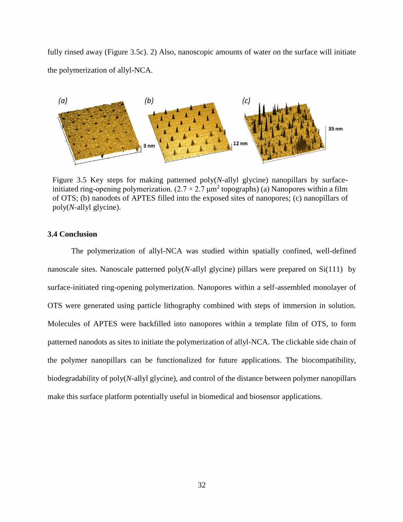
32
fully rinsed away (Figure 3.5c). 2) Also, nanoscopic amounts of water on the surface will initiate
the polymerization of allyl-NCA.
3.4 Conclusion
The polymerization of allyl-NCA was studied within spatially confined, well-defined
nanoscale sites. Nanoscale patterned poly(N-allyl glycine) pillars were prepared on Si(111) by
surface-initiated ring-opening polymerization. Nanopores within a self-assembled monolayer of
OTS were generated using particle lithography combined with steps of immersion in solution.
Molecules of APTES were backfilled into nanopores within a template film of OTS, to form
patterned nanodots as sites to initiate the polymerization of allyl-NCA. The clickable side chain of
the polymer nanopillars can be functionalized for future applications. The biocompatibility,
biodegradability of poly(N-allyl glycine), and control of the distance between polymer nanopillars
make this surface platform potentially useful in biomedical and biosensor applications.
Figure 3.5 Key steps for making patterned poly(N-allyl glycine) nanopillars by surface-
initiated ring-opening polymerization. (2.7 × 2.7 μm2 topographs) (a) Nanopores within a film
of OTS; (b) nanodots of APTES filled into the exposed sites of nanopores; (c) nanopillars of
poly(N-allyl glycine).

33
CHAPTER 4. THERMO-RESPONSIVE BEHAVIOR OF LINEAR COPOLYPEPTOID
NANOSTRUCTURES INVESTIGATED WITH ATOMIC FORCE MICROSCOPY
4.1 Introduction
Thermo-responsive surfaces formed by polymeric materials have received recent attention
due to the potential applications.159 Among the polymeric materials, poly(N-isopropyl acrylamide),
or PNIPAAm, is the most often studied system due to its lower critical solution temperature (LCST
of 32 C), just below the human physiological temperature (37 C).160-163 Temperature-responsive
surfaces prepared with PNIPAAm have been investigated for applications in tissue culture and
microfluidics,164-165 display and sensor technology,166 cell-seeding and co-culture.167 Surface
grafted PNIPAAm on regenerated cellulose membranes have thermally modulated permeability.168
Responsive copolymer systems having PNIPAAm segment have been studied.169-174 For example,
poly(N-isopropylacrylamide-co-dopamine methacrylamide) was synthesized and attached to a Si
wafer for cell sheet applications.169 A gold nanoparticle with surface-linked poly(styrene-b-N-
isopropylacrylamide) copolymer formed temperature-responsive core-shell micelles.170 Other
thermo-responsive polymers have been used to make stimuli-responsive surfaces, including
poly[di(ethyleneglycol)methyl ether methacrylate],175 poly[oligo(ethylene oxide)monomethyl
ether methacrylate]-based star polymers,176 gradient and block copolymers based on 2-(2-
methoxyethoxy)ethyl methacrylate,177 acetylated
poly-N-[tris(hydroxymethyl)methyl] acrylamide,178 as well as other systems.179-181
The two common methods to decorate surfaces with polymer are the “grafting from” and
“grafting to” methods. The “grafting from” method, usually occurs through a surface-initiated
polymerization of selected monomers. Using this method, the grafting density is nearly
quantitative, but at the expense of control of the polymer brushes (which tend to have broader
molecular weight distributions than polymer brushes from the “grafting to” method).182 The
34
“grafting to” approach involves the coupling reaction between surface reactive moieties and the
end-groups of functionalized polymer. Though this method having the advantages of controlling
the brush polymer molecular weight, architecture and microstructure, high grafting densities are
compromised due to steric crowding.
Many “grafting to” approaches use click reactions to prepare surface tethered polymer
brushes because the reaction proceeds with high yields and no byproducts.183-185 Among several
types of click reactions, the copper (Ι) catalyzed azide-alkyne cycloaddition (CuAAC) is most
widely used.186-196 Three examples of CuAAC are ligand α-acetylene-poly(tert-butyl acrylate) with
alkyne end group attached to azide functionalized γ-Fe2O3 nanoparticles,197 temperature sensitive
nanocomposites of immobilizing thermo-responsive PNIPAAm on Au nanoparticles,198 and
polystyrene/polyacrylamide functionalized silica nanoparticles with the combination of living
radical/tandem polymerization and azide-alkyne click reaction.199-200 Azide-alkyne and thiol-ene
click reaction can be used at the same time, as demonstrated previously by others, to form binary
polymer brushes on silica spheres, followed by removal of the inorganic silica core in hydrogen
fluoride solution to obtain hollow polymer nanospheres.201 The thiol-ene click reaction is a less
commonly used click coupling reaction. However, this reaction is still a efficient, rapid and nearly
quantitative method to tether polymers to surfaces.202-204 A major advantage of thiol-ene chemistry
is that this method leaves no trace metal residues in the system as compared with azide-alkyne
reaction.202-204 As demonstrated with poly(oligo(ethylene glycol)methyl ether methacrylate)
coated titanium dioxide nanoparticles, the thiol-ene reaction can reduce particle aggregation and
cellular uptake as well as diminish cytotoxicity.205
Thiol-functionalized linear random copolypeptoid poly[(N-ethyl glycine)32-r-(N-butyl
glycine17)], or P(NEG32-r-NBG17), was synthesized in solution phase. Particle lithography and
35
thiol-ene click reaction were combined to pattern the copolypeptoids on a surface. The thermo-
responsiveness of patterned copolypeptoids was studied using in situ atomic force microscopy
(AFM). Unlike homogeneous film on surface, this work shows the thermo-responsiveness of the
polymer nanopillars on surface are more pronounced and easier to detect. The in situ studies of the
thermo-responsiveness of patterned polymer pillars at the nanoscale will be discussed for the first
time.
4.2 Experimental Section
4.2.1 Preparation of Nanopatterned UTS Sites
Nanopores within a thin film of OTS on Si wafer were prepared with a previously reported
method.206 The diameter of the silica mesospheres used in the experiment is 0.49 ± 0.02 μm (Duke,
Inc. Fremont, CA). The substrate with OTS nanopore patterns was characterized with AFM and
the result is shown in Appendix Figure C1. The patterned bare areas of the Si substrate were
backfilled with UTS by immersing substrate in UTS solution (0.1% v/v solution of UTS in
bicyclohexyl) for 5 h. Next, the sample was rinsed with three solvents (water, THF and ethanol),
followed by sonication in ethanol and sonication in water to remove excess amount of silane. The
sample was characterized with contact-mode AFM in air.
4.2.2 Synthesis of Linear poly[(N-ethyl glycine)32-r-(N-butyl glycine)17] Copolymer
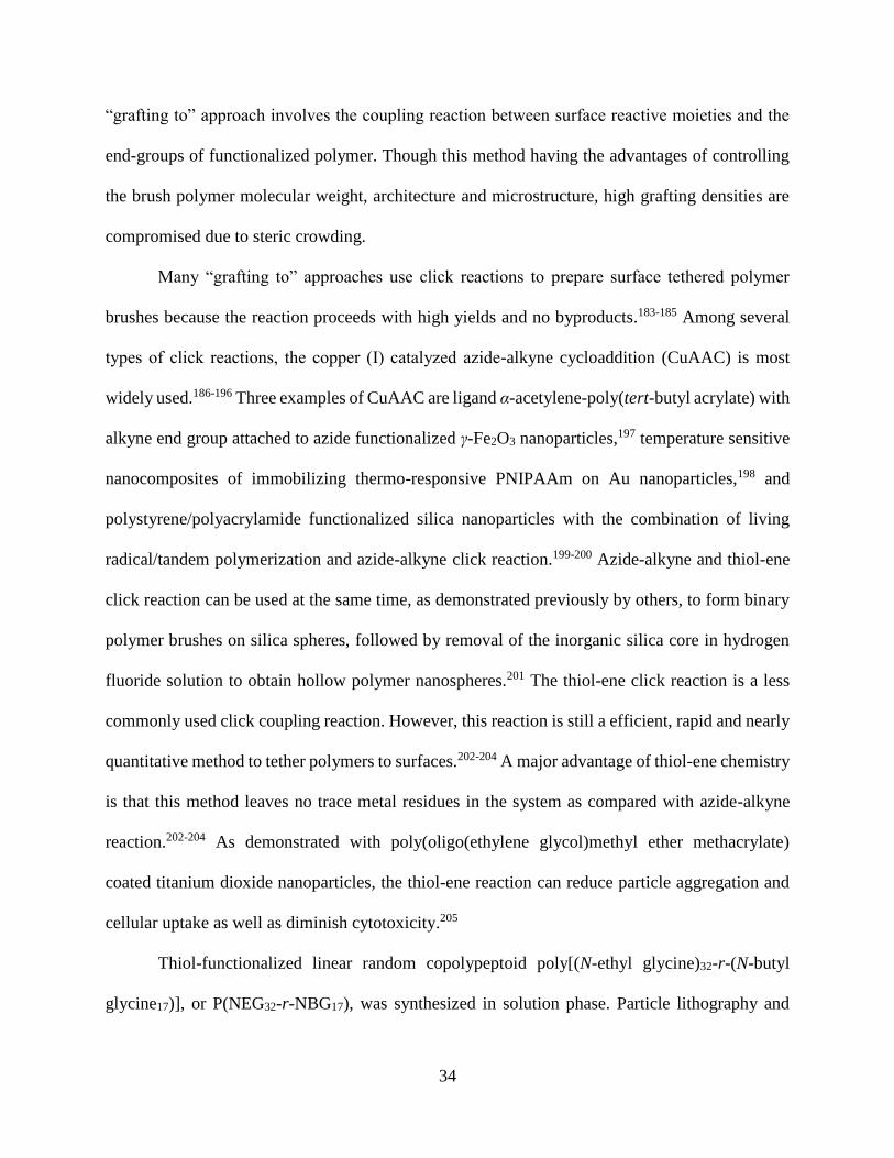
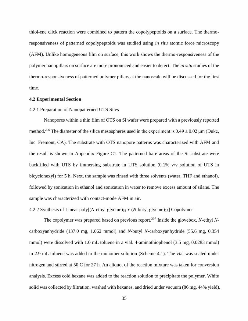
The copolymer was prepared based on previous report.207 Inside the glovebox, N-ethyl N-
carboxyanhydride (137.0 mg, 1.062 mmol) and N-butyl N-carboxyanhydride (55.6 mg, 0.354
mmol) were dissolved with 1.0 mL toluene in a vial. 4-aminothiophenol (3.5 mg, 0.0283 mmol)
in 2.9 mL toluene was added to the monomer solution (Scheme 4.1). The vial was sealed under
nitrogen and stirred at 50 C for 27 h. An aliquot of the reaction mixture was taken for conversion
analysis. Excess cold hexane was added to the reaction solution to precipitate the polymer. White
solid was collected by filtration, washed with hexanes, and dried under vacuum (86 mg, 44% yield).
36
Size exclusive chromatography (Mw = 14.5 kDa, PDI = 1.24). 1H NMR (δ in CD2Cl2, ppm): 0.82-
1.00 (bt, CH3CH2-, NBG), 1.05-1.21 (bt, CH3CH2-, NEG), 1.23-1.70 (bm, -CH2CH2CH3), 3.13-
3.64 (bm, - NCH2CH3, -NCH2CH2-), 3.88-4.43 (bm, -COCH2-). (1H NMR spectrum in Appendix
Figure C4).
4.2.3 Preparation Nanopatterned Poly[(N-ethyl glycine)32-r-(N-butyl glycine)17] by Surface
Thiol-ene Click Reaction
Copolymer (10 mg) and photoinitiator Irgacure (10 mg) were added in 2 mL of THF. Si
substrate with UTS patterns was immersed in the THF solution and placed under UV lamp (Xenon
Arc Lamp) overnight (18 h). Substrate was then rinsed with THF and sonicated, first in THF and
second in ethanol. The sample was characterized with AFM the contact-mode in water.
4.2.4 Thermoresponsive Study of Nanopatterned Copolypeptoids using in situ AFM
A sample stage with a water-filled liquid cell is used to hold sample of patterned
copolypeptoids on Si wafer. A temperature controller is connected with the sample stage which
can adjust the temperature of the sample plate, as well as the sample. The polymer nanopillar
height and morphology changes of the copolypeptoids with the increase of temperature were
tracked with in situ AFM.
Scheme 4.1 Copolymerize N-ethyl N-carboxyanhydride and N-butyl N-carboxyanhydride
with initiator 4-aminothiophenol.
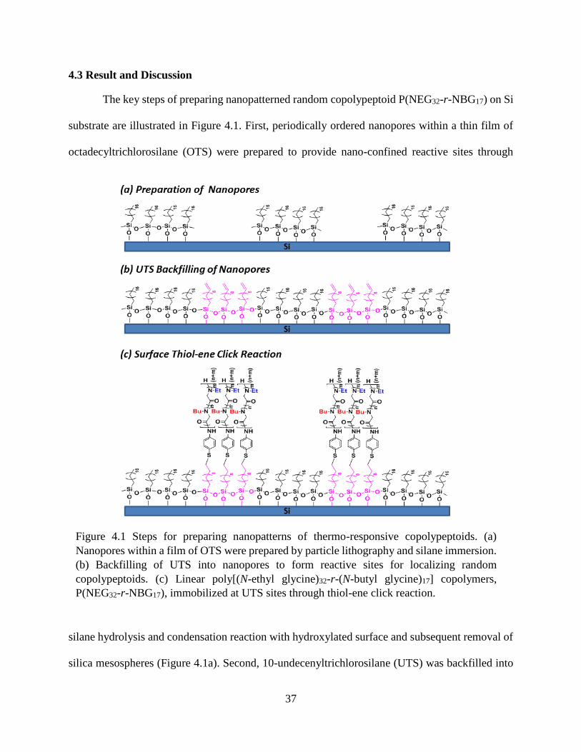
37
4.3 Result and Discussion
The key steps of preparing nanopatterned random copolypeptoid P(NEG32-r-NBG17) on Si
substrate are illustrated in Figure 4.1. First, periodically ordered nanopores within a thin film of
octadecyltrichlorosilane (OTS) were prepared to provide nano-confined reactive sites through
silane hydrolysis and condensation reaction with hydroxylated surface and subsequent removal of
silica mesospheres (Figure 4.1a). Second, 10-undecenyltrichlorosilane (UTS) was backfilled into
Figure 4.1 Steps for preparing nanopatterns of thermo-responsive copolypeptoids. (a)
Nanopores within a film of OTS were prepared by particle lithography and silane immersion.
(b) Backfilling of UTS into nanopores to form reactive sites for localizing random
copolypeptoids. (c) Linear poly[(N-ethyl glycine)32-r-(N-butyl glycine)17] copolymers,
P(NEG32-r-NBG17), immobilized at UTS sites through thiol-ene click reaction.
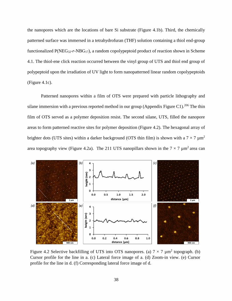
38
the nanopores which are the locations of bare Si substrate (Figure 4.1b). Third, the chemically
patterned surface was immersed in a tetrahydrofuran (THF) solution containing a thiol end-group
functionalized P(NEG32-r-NBG17), a random copolypeptoid product of reaction shown in Scheme
4.1. The thiol-ene click reaction occurred between the vinyl group of UTS and thiol end group of
polypeptoid upon the irradiation of UV light to form nanopatterned linear random copolypeptoids
(Figure 4.1c).
Patterned nanopores within a film of OTS were prepared with particle lithography and
silane immersion with a previous reported method in our group (Appendix Figure C1).206 The thin
film of OTS served as a polymer deposition resist. The second silane, UTS, filled the nanopore
areas to form patterned reactive sites for polymer deposition (Figure 4.2). The hexagonal array of
brighter dots (UTS sites) within a darker background (OTS thin film) is shown with a 7 × 7 µm2
area topography view (Figure 4.2a). The 211 UTS nanopillars shown in the 7 × 7 µm2 area can
Figure 4.2 Selective backfilling of UTS into OTS nanopores. (a) 7 × 7 µm2 topograph. (b)
Cursor profile for the line in a. (c) Lateral force image of a. (d) Zoom-in view. (e) Cursor
profile for the line in d. (f) Corresponding lateral force image of d.
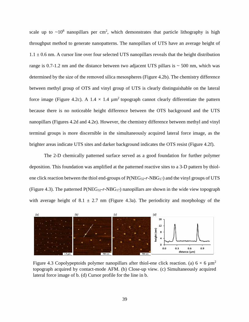
39
scale up to ~108 nanopillars per cm2, which demonstrates that particle lithography is high
throughput method to generate nanopatterns. The nanopillars of UTS have an average height of
1.1 ± 0.6 nm. A cursor line over four selected UTS nanopillars reveals that the height distribution
range is 0.7-1.2 nm and the distance between two adjacent UTS pillars is ~ 500 nm, which was
determined by the size of the removed silica mesospheres (Figure 4.2b). The chemistry difference
between methyl group of OTS and vinyl group of UTS is clearly distinguishable on the lateral
force image (Figure 4.2c). A 1.4 × 1.4 µm2 topograph cannot clearly differentiate the pattern
because there is no noticeable height difference between the OTS background and the UTS
nanopillars (Figures 4.2d and 4.2e). However, the chemistry difference between methyl and vinyl
terminal groups is more discernible in the simultaneously acquired lateral force image, as the
brighter areas indicate UTS sites and darker background indicates the OTS resist (Figure 4.2f).
The 2-D chemically patterned surface served as a good foundation for further polymer
deposition. This foundation was amplified at the patterned reactive sites to a 3-D pattern by thiol-
ene click reaction between the thiol end-groups of P(NEG32-r-NBG17) and the vinyl groups of UTS
(Figure 4.3). The patterned P(NEG32-r-NBG17) nanopillars are shown in the wide view topograph
with average height of 8.1 ± 2.7 nm (Figure 4.3a). The periodicity and morphology of the
Figure 4.3 Copolypeptoids polymer nanopillars after thiol-ene click reaction. (a) 6 × 6 µm2
topograph acquired by contact-mode AFM. (b) Close-up view. (c) Simultaneously acquired
lateral force image of b. (d) Cursor profile for the line in b.
40
copolypeptoid nanopillars on surface are shown in the 2.5 × 2.5 µm2 topography view (Figure
4.3b). The chemistry difference between polypeptoid nanopillars and OTS background can be
clearly seen in the corresponding lateral force image (Figure 4.3c). Two selected polymer
nanopillar areas (see cursor line in Figure 4.3b) have measured a height of ~11 nm and at a distance
of ~540 nm (Figure 4.3d). The inhomogeneity of a single polypeptoid nanopillar site in the lateral
force image indicates that there are many polymer brushes at one nanopore site with an upright
orientation.
The thermo-responsiveness of the linear random copolypeptoid P(NEG32-r-NBG17) was
investigated using in situ AFM in aqueous media after patterning of the polymer brushes on Si
surface. As the temperature of the liquid media surrounding the Si substrate was ramped at 5 C
increments, the height of the polypeptoid nanostructures appeared to change. The results at three
selected temperatures (25 C, 45 C and 65 C) are shown in Figure 4.4 and more temperature studies
are shown in Appendix C (Figure C2). The heights decrease of two particular polymer brush sites
were monitored and indicated in the topographs (Figures 4.4a, c and e) and cursor profiles (Figures
4.4b, d, and f). At 25 C, the heights of the two nanostructures vary (Figure 4.4b), which is
according to the original size of the nanoholes within OTS. The polymer brushes collapsed upon
heating, as indicated by a nanopillar height decrease from more than 10 nm (25 C) to less than 3
nm (65 C).
The LCST behavior of the copolypeptoid was also studied with the turbidity assay using
untethered copolymer in aqueous solution. The onset cloud point temperature (Tcp), the
temperature measured at 90% transmittance, is 45 C for a solution of copolypeptoid (1 mg•mL-1
in water) (Appendix Figure C3). Changes in the composition of copolypeptoids can be used to
adjust the cloud point temperature within the range of 20-60 C. In aqueous solution, the unbound
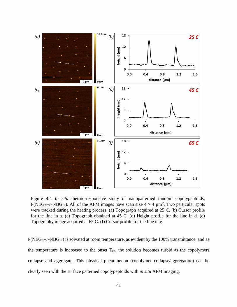
41
P(NEG32-r-NBG17) is solvated at room temperature, as evident by the 100% transmittance, and as
the temperature is increased to the onset Tcp, the solution becomes turbid as the copolymers
collapse and aggregate. This physical phenomenon (copolymer collapse/aggregation) can be
clearly seen with the surface patterned copolypeptoids with in situ AFM imaging.
Figure 4.4 In situ thermo-responsive study of nanopatterned random copolypeptoids,
P(NEG32-r-NBG17). All of the AFM images have scan size 4 × 4 µm2. Two particular spots
were tracked during the heating process. (a) Topograph acquired at 25 C. (b) Cursor profile
for the line in a. (c) Topograph obtained at 45 C. (d) Height profile for the line in d. (e)
Topography image acquired at 65 C. (f) Cursor profile for the line in g.
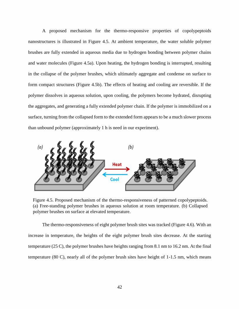
42
A proposed mechanism for the thermo-responsive properties of copolypeptoids
nanostructures is illustrated in Figure 4.5. At ambient temperature, the water soluble polymer
brushes are fully extended in aqueous media due to hydrogen bonding between polymer chains
and water molecules (Figure 4.5a). Upon heating, the hydrogen bonding is interrupted, resulting
in the collapse of the polymer brushes, which ultimately aggregate and condense on surface to
form compact structures (Figure 4.5b). The effects of heating and cooling are reversible. If the
polymer dissolves in aqueous solution, upon cooling, the polymers become hydrated, disrupting
the aggregates, and generating a fully extended polymer chain. If the polymer is immobilized on a
surface, turning from the collapsed form to the extended form appears to be a much slower process
than unbound polymer (approximately 1 h is need in our experiment).
The thermo-responsiveness of eight polymer brush sites was tracked (Figure 4.6). With an
increase in temperature, the heights of the eight polymer brush sites decrease. At the starting
temperature (25 C), the polymer brushes have heights ranging from 8.1 nm to 16.2 nm. At the final
temperature (80 C), nearly all of the polymer brush sites have height of 1-1.5 nm, which means
Figure 4.5. Proposed mechanism of the thermo-responsiveness of patterned copolypeptoids.
(a) Free-standing polymer brushes in aqueous solution at room temperature. (b) Collapsed
polymer brushes on surface at elevated temperature.

43
the length of the polymer brush in our experiment does not influence the trend of decreasing in
height of the random copolypeptoid P(NEG32-r-NBG17) with increasing in temperature.
4.4 Conclusion
In conclusion, to the best of our knowledge, for the very first time, the thermo-
responsiveness of patterned polymer brushes at the nanoscale was studied in situ. Thiol-ene click
chemistry turned out an efficient way to attach functionalized linear polymer, in our case, the
random copolypeptoid poly[(N-ethyl glycine)32-r-(N-butyl glycine17)], or P(NEG32-r-NBG17), to
the substrates. The surface changes at nanoscale can be sensitively detected with AFM when
increasing temperature to 35 C. However, the transmittance change only can be noticed after 45 C
at eh onset cloud point temperature.
Figure 4.6 Temperature-dependent changes in height studied in situ with AFM. (left) Example
topograph at 25 C. The heights of eight polymer brush sites were tracked. (right)
Measurements for height decrease with rising temperature (C).
44
CHAPTER 5. A REVIEW ON FORCE MODULATION MICROSCOPY AND THE
CAPABILITY OF NANOMECHANICAL MAPPING OF SURFACE ELASTIC AND
VISCOELASTIC PROPERTIES
5.1 History of Force Modulation Microscopy (FMM)
Since its invention in 1986, atomic force microscopy (AFM) has been used in a broad range
of fields for surface characterizations.1 Force modulation microscopy (FMM), one of over 50
possible modes of AFM, was invented in 1991 by Maivald and Hansma et al. to study the carbon
fiber and epoxy composite.14
With FMM, local mechanical properties of a sample surface can be acquired along with
topography by imposing a z axis vibration between tip-sample contact during contact-mode
imaging. Dynamic response of the sample to an increased or decreased load is monitored. In the
first report of FMM, variations in the local elasticity were differentiated on a composite surface at
the nanoscale.14 The sample was placed on a piezoelectric translator and the AFM tip was raster
scanned across the sample surface in contact-mode with constant force. At the same time, a z axis
vibration of 25 nm was introduced to the sample through the z piezoelement. The frequency of the
z axis vibration was tuned so that it did not interfere with the resonance frequencies of the feedback
loop and minimized the coupling with the electronics. The cantilever deflection is larger on the
harder regions compared with softer regions during FMM, because more pressing energy from the
cantilever can be absorbed by the soft regions and more deformation was encountered by the soft
regions. Clear contrast was acquired in the amplitude image and the elasticity modulus of carbon
fibers and epoxy were estimated.
Due to the relative high forces (10-7-10-6 N) applied during contact-mode AFM, images of
soft materials suffer from insufficient contrast and quality. The author who did the earliest work
of FMM realized that: since soft materials like biological samples are usually deposited on hard
substrates for AFM work, the FMM increases the potential of imaging soft materials because of
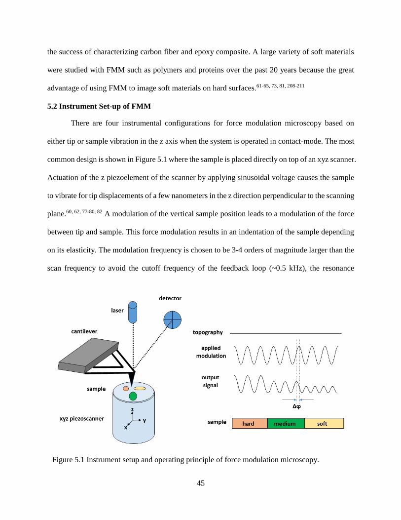
45
the success of characterizing carbon fiber and epoxy composite. A large variety of soft materials
were studied with FMM such as polymers and proteins over the past 20 years because the great
advantage of using FMM to image soft materials on hard surfaces.61-65, 73, 81, 208-211
5.2 Instrument Set-up of FMM
There are four instrumental configurations for force modulation microscopy based on
either tip or sample vibration in the z axis when the system is operated in contact-mode. The most
common design is shown in Figure 5.1 where the sample is placed directly on top of an xyz scanner.
Actuation of the z piezoelement of the scanner by applying sinusoidal voltage causes the sample
to vibrate for tip displacements of a few nanometers in the z direction perpendicular to the scanning
plane.60, 62, 77-80, 82 A modulation of the vertical sample position leads to a modulation of the force
between tip and sample. This force modulation results in an indentation of the sample depending
on its elasticity. The modulation frequency is chosen to be 3-4 orders of magnitude larger than the
scan frequency to avoid the cutoff frequency of the feedback loop (~0.5 kHz), the resonance
Figure 5.1 Instrument setup and operating principle of force modulation microscopy.

46
frequency of the piezoscanner (~8 kHz) and the cutoff frequency of the photodetector (~1 MHz).62
Soft probes with spring constants less than 1 N/m are usually used in FMM studies because of the
possibility of plastic deformation (wear) of the polymer surface.84 The oscillation amplitude is kept
small so that the topography image will not be degraded by vibration at tip-sample contact.
A flat surface with three regions of varying elastic moduli is shown as a proof-of-concept
in Figure 5.1. From the FMM topograph, a flat surface without any contrast will be resolved.
Comparing to the input sinusoidal wave signal, the output signal has an amplitude change and a
phase angle shift which are detected by two lock-in amplifiers and translate to FMM amplitude
and FMM phase images. Careful comparisons between FMM topographs with contact-mode
topographs have been made and no significant differences were found.83
In the second instrument configuration for FMM, a cantilever holder equipped with
bimorph piezoelements, which can actuate the tip as it is pressed against the sample, is used.63, 74,
83-84 The bimorph piezos can oscillate the cantilever near resonance frequency during tapping-
mode and depress the tip into the sample surface during FMM.63 Therefore, two modes are enabled
using the same set-up.
The third way to accomplish force modulation imaging is using a magnetic field to drive
the vibration of a tip or tip-holder assembly.85-88, 212 In Yamamoto’s work, samples were mounted
on a piezoelectric tube scanner, inside of which a coil for an electromagnet was fixed. A piece of
samarium cobolt magnet was glued at the end of the backside of the cantilever.85 In Pietrement’s
work, the solenoid was placed around the piezotube and a small spherical magnetic particle of
LaNdFeB alloy was glued on the backside of the cantilever just above the tip.213 Indirect magnetic
modulation (IMM), invented by Li et al., is another instrument configuration for FMM.86 The
47
entire tip assembly, containing ferromagnetic materials, is induced to vibrate with the flux of an
external AC electromagntetic field, generated by a wire coil solenoid underneath the sample plate.
The fourth design is a scan-by-tip AFM configuration, the z axis vibration is applied to the
sample. Troyon and Hazotte et al. placed a transducer underneath the sample, which is a 0.5 mm
thick and 8 mm round disk.76 Lu and Garno et al. embedded a piezoactuator inside a machined
polycarbonate sample stage to generate the z axis vibration by applying AC current to the
piezoelement.
5.3 Advantages of FMM
Force modulation can be used for identifying and mapping differences in stiffness or
elasticity, evaluating materials’ homogeneities,85, 214 and studying variations in crystallinity,6
polymer phase separation, surface arrangement and distribution.80, 215-217 Mechanical properties of
the surfaces are probed continuously over extended areas instead of at scattered individual points
as in force-distance curves and load-indentation measurements.83 Asif and Colton et al. combined
nanoindentation and force modulation microscopy together to acquire nanoscale mechanical
properties.218-219 In force-distance curve measurement, the probe is not perfectly perpendicular to
the sample due to the 10-15° tilt of the cantilever. Therefore, the load has a tangential component
in the direction parallel to the cantilever arm, which induces error measurements.213 To overcome
the scanning angle problem in FMM, Overney and Fijihira et al. added an additional piezo plate
between the piezoscanner and sample so the z modulation direction can be freely adjusted within
90° by tilting the piezo plane.78
Force modulation microscopy can also quantify information about sample surfaces such as
Young’s modulus and elasticity.75-76, 79, 213 An example of calculating the spring constant of sample
surface is given here.79 For FMM when the sample is modulating in the z axis on top of a piezotube,
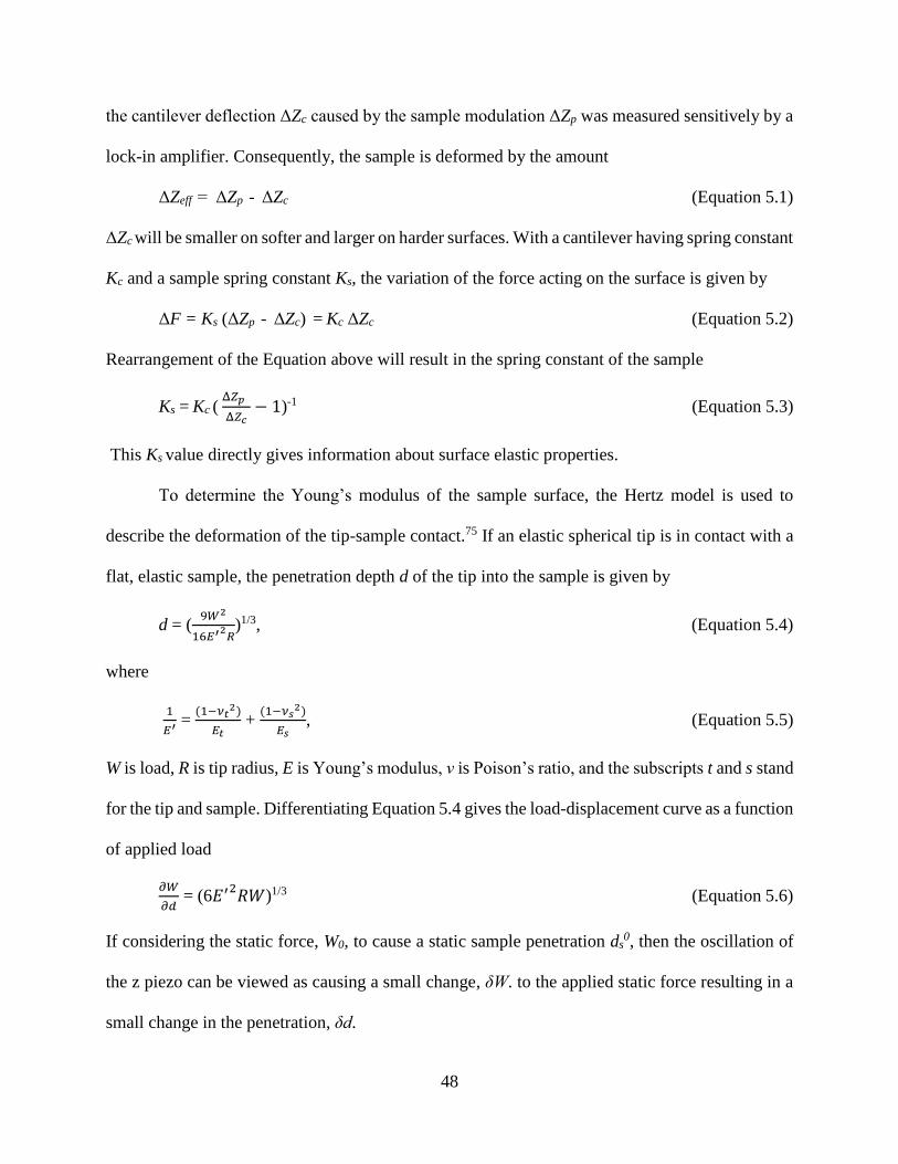
48
the cantilever deflection ΔZc caused by the sample modulation ΔZp was measured sensitively by a
lock-in amplifier. Consequently, the sample is deformed by the amount
ΔZeff = ΔZp - ΔZc (Equation 5.1)
ΔZc will be smaller on softer and larger on harder surfaces. With a cantilever having spring constant
Kc and a sample spring constant Ks, the variation of the force acting on the surface is given by
ΔF = Ks (ΔZp - ΔZc) = Kc ΔZc (Equation 5.2)
Rearrangement of the Equation above will result in the spring constant of the sample
Ks = Kc ( Δ𝑍𝑝
Δ𝑍𝑐− 1)-1 (Equation 5.3)
This Ks value directly gives information about surface elastic properties.
To determine the Young’s modulus of the sample surface, the Hertz model is used to
describe the deformation of the tip-sample contact.75 If an elastic spherical tip is in contact with a
flat, elastic sample, the penetration depth d of the tip into the sample is given by
d = (9𝑊2
16𝐸′2𝑅)1/3, (Equation 5.4)
where
1
𝐸′ = (1−𝜈𝑡
2)
𝐸𝑡 +
(1−𝜈𝑠2)
𝐸𝑠, (Equation 5.5)
W is load, R is tip radius, E is Young’s modulus, ν is Poison’s ratio, and the subscripts t and s stand
for the tip and sample. Differentiating Equation 5.4 gives the load-displacement curve as a function
of applied load
𝜕𝑊
𝜕𝑑 = (6𝐸′2
𝑅𝑊)1/3 (Equation 5.6)
If considering the static force, W0, to cause a static sample penetration ds0, then the oscillation of
the z piezo can be viewed as causing a small change, δW. to the applied static force resulting in a
small change in the penetration, δd.
49
𝛿𝑊
𝛿𝑑 = (6𝐸′2
𝑅𝑊0)1/3 (Equation 5.7)
δW = 𝑘𝑐 𝑑𝑐 (Equation 5.8)
δd = 𝑑𝑠 = 𝑑𝑏 - 𝑑𝑐 (Equation 5.9)
𝑊0 = 𝑘𝑐 𝑑𝑐0 + 𝑊𝑎 (Equation 5.10)
where 𝑑𝑐 is cantilever deflection, 𝑘𝑐 is cantilever spring constant, 𝑑𝑠 is sample penetration depth,
𝑑𝑏 is the oscillation of the bimorph piezo, 𝑊𝑎 is adhesion force, and the static force 𝑊0 applied by
the cantilever can be related to the mean deflection of the cantilever 𝑑𝑐0. By applying Equations
8-10 to Equation 7 a quantitative measurement of Young’s modulus is made:
𝐸′ = [6(𝑑𝑏 − 𝑑𝑐
𝑘𝑐 𝑑𝑐)3R(𝑘𝑐 𝑑𝑐
0 + 𝑊𝑎)]-1/2 (Equation 5.11)
5.4 Studying Self-assembled Monolayers (SAMs) Using FMM
The surface elastic and viscoelastic properties of self-assembled monolayers (SAMs) are
widely studied with FMM. Some FMM work in SAM systems are summarized in Table 5.1. Bi-
functional surfaces of Langmuir-Blodgett (LB) film comprised of two kinds of molecules were
used as samples to probe the elasticity and viscoelasticity using FMM. Most of the systems were
investigated using the z piezoelement to generate the z axis vibration of the samples. Either
qualitative comparison between two components’ elasticities or quantitative information about the
Young’s modulus were acquired. Vibration amplitude of a few nanometers was used, which is
much smaller than tapping-mode. The vibrational frequency was chosen to be much higher than
imaging speed but avoid interference with the feedback loop. Commonly a cantilever with a small
spring constant (<1 N/m) is used.
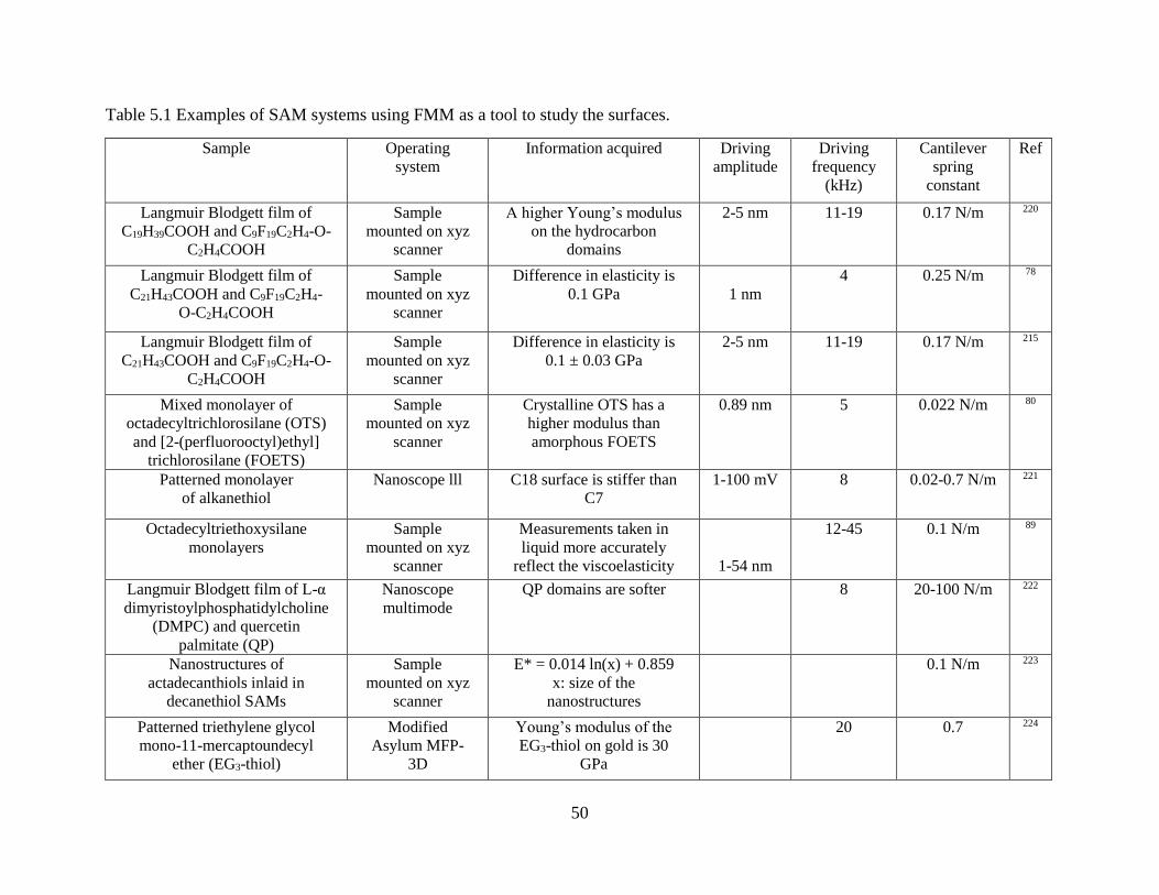
50
Table 5.1 Examples of SAM systems using FMM as a tool to study the surfaces.
Sample
Operating
system
Information acquired Driving
amplitude
Driving
frequency
(kHz)
Cantilever
spring
constant
Ref
Langmuir Blodgett film of
C19H39COOH and C9F19C2H4-O-
C2H4COOH
Sample
mounted on xyz
scanner
A higher Young’s modulus
on the hydrocarbon
domains
2-5 nm 11-19 0.17 N/m 220
Langmuir Blodgett film of
C21H43COOH and C9F19C2H4-
O-C2H4COOH
Sample
mounted on xyz
scanner
Difference in elasticity is
0.1 GPa
1 nm
4 0.25 N/m 78
Langmuir Blodgett film of
C21H43COOH and C9F19C2H4-O-
C2H4COOH
Sample
mounted on xyz
scanner
Difference in elasticity is
0.1 ± 0.03 GPa
2-5 nm 11-19 0.17 N/m 215
Mixed monolayer of
octadecyltrichlorosilane (OTS)
and [2-(perfluorooctyl)ethyl]
trichlorosilane (FOETS)
Sample
mounted on xyz
scanner
Crystalline OTS has a
higher modulus than
amorphous FOETS
0.89 nm 5 0.022 N/m 80
Patterned monolayer
of alkanethiol
Nanoscope lll C18 surface is stiffer than
C7
1-100 mV 8 0.02-0.7 N/m 221
Octadecyltriethoxysilane
monolayers
Sample
mounted on xyz
scanner
Measurements taken in
liquid more accurately
reflect the viscoelasticity
1-54 nm
12-45 0.1 N/m 89
Langmuir Blodgett film of L-α
dimyristoylphosphatidylcholine
(DMPC) and quercetin
palmitate (QP)
Nanoscope
multimode
QP domains are softer
8 20-100 N/m 222
Nanostructures of
actadecanthiols inlaid in
decanethiol SAMs
Sample
mounted on xyz
scanner
E* = 0.014 ln(x) + 0.859
x: size of the
nanostructures
0.1 N/m 223
Patterned triethylene glycol
mono-11-mercaptoundecyl
ether (EG3-thiol)
Modified
Asylum MFP-
3D
Young’s modulus of the
EG3-thiol on gold is 30
GPa
20 0.7 224
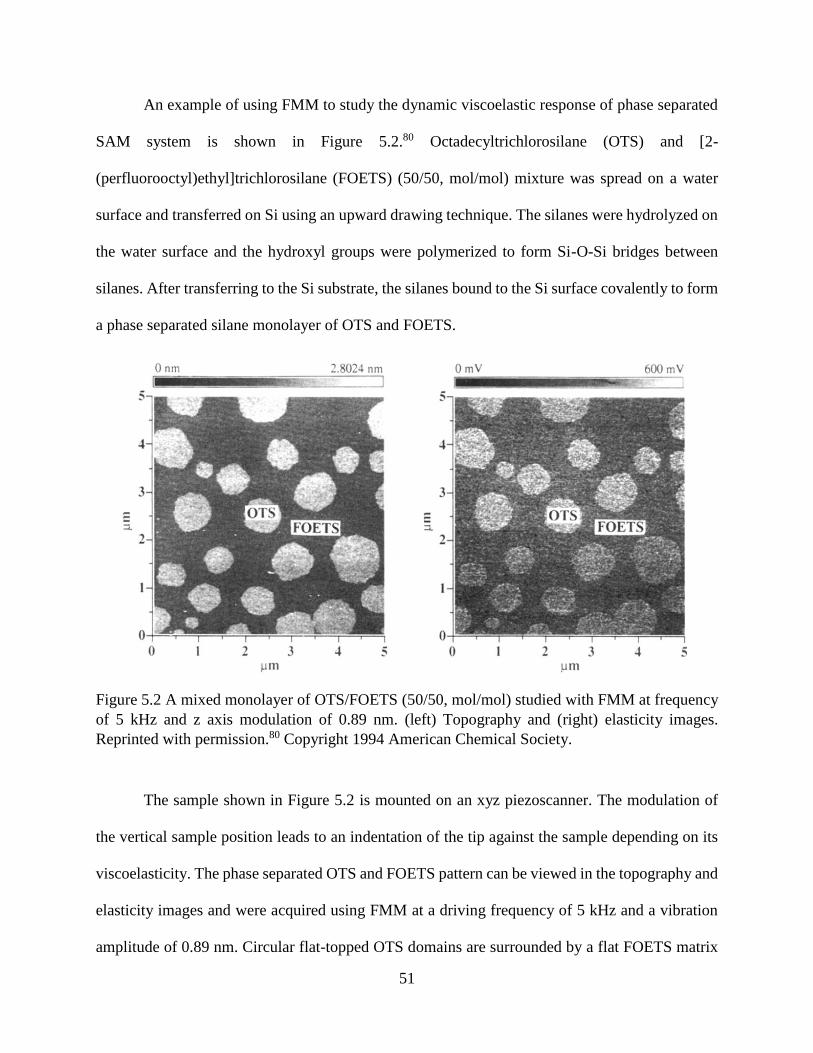
51
An example of using FMM to study the dynamic viscoelastic response of phase separated
SAM system is shown in Figure 5.2.80 Octadecyltrichlorosilane (OTS) and [2-
(perfluorooctyl)ethyl]trichlorosilane (FOETS) (50/50, mol/mol) mixture was spread on a water
surface and transferred on Si using an upward drawing technique. The silanes were hydrolyzed on
the water surface and the hydroxyl groups were polymerized to form Si-O-Si bridges between
silanes. After transferring to the Si substrate, the silanes bound to the Si surface covalently to form
a phase separated silane monolayer of OTS and FOETS.
Figure 5.2 A mixed monolayer of OTS/FOETS (50/50, mol/mol) studied with FMM at frequency
of 5 kHz and z axis modulation of 0.89 nm. (left) Topography and (right) elasticity images.
Reprinted with permission.80 Copyright 1994 American Chemical Society.
The sample shown in Figure 5.2 is mounted on an xyz piezoscanner. The modulation of
the vertical sample position leads to an indentation of the tip against the sample depending on its
viscoelasticity. The phase separated OTS and FOETS pattern can be viewed in the topography and
elasticity images and were acquired using FMM at a driving frequency of 5 kHz and a vibration
amplitude of 0.89 nm. Circular flat-topped OTS domains are surrounded by a flat FOETS matrix
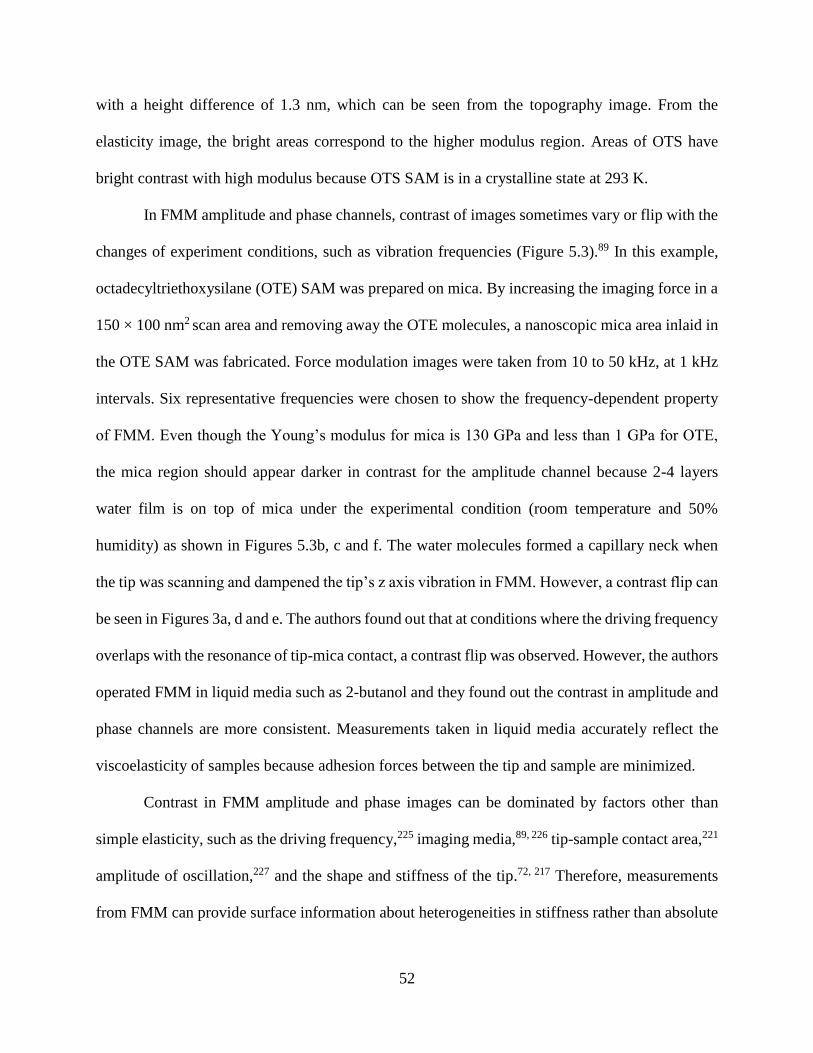
52
with a height difference of 1.3 nm, which can be seen from the topography image. From the
elasticity image, the bright areas correspond to the higher modulus region. Areas of OTS have
bright contrast with high modulus because OTS SAM is in a crystalline state at 293 K.
In FMM amplitude and phase channels, contrast of images sometimes vary or flip with the
changes of experiment conditions, such as vibration frequencies (Figure 5.3).89 In this example,
octadecyltriethoxysilane (OTE) SAM was prepared on mica. By increasing the imaging force in a
150 × 100 nm2 scan area and removing away the OTE molecules, a nanoscopic mica area inlaid in
the OTE SAM was fabricated. Force modulation images were taken from 10 to 50 kHz, at 1 kHz
intervals. Six representative frequencies were chosen to show the frequency-dependent property
of FMM. Even though the Young’s modulus for mica is 130 GPa and less than 1 GPa for OTE,
the mica region should appear darker in contrast for the amplitude channel because 2-4 layers
water film is on top of mica under the experimental condition (room temperature and 50%
humidity) as shown in Figures 5.3b, c and f. The water molecules formed a capillary neck when
the tip was scanning and dampened the tip’s z axis vibration in FMM. However, a contrast flip can
be seen in Figures 3a, d and e. The authors found out that at conditions where the driving frequency
overlaps with the resonance of tip-mica contact, a contrast flip was observed. However, the authors
operated FMM in liquid media such as 2-butanol and they found out the contrast in amplitude and
phase channels are more consistent. Measurements taken in liquid media accurately reflect the
viscoelasticity of samples because adhesion forces between the tip and sample are minimized.
Contrast in FMM amplitude and phase images can be dominated by factors other than
simple elasticity, such as the driving frequency,225 imaging media,89, 226 tip-sample contact area,221
amplitude of oscillation,227 and the shape and stiffness of the tip.72, 217 Therefore, measurements
from FMM can provide surface information about heterogeneities in stiffness rather than absolute
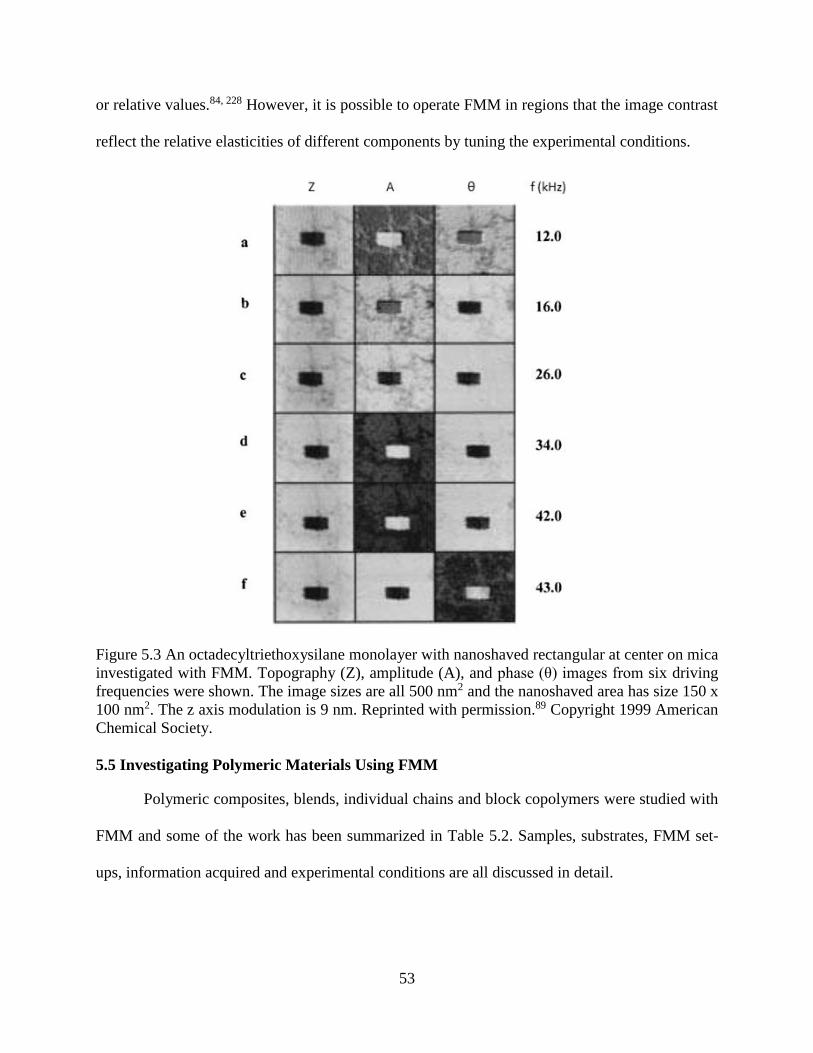
53
or relative values.84, 228 However, it is possible to operate FMM in regions that the image contrast
reflect the relative elasticities of different components by tuning the experimental conditions.
Figure 5.3 An octadecyltriethoxysilane monolayer with nanoshaved rectangular at center on mica
investigated with FMM. Topography (Z), amplitude (A), and phase (θ) images from six driving
frequencies were shown. The image sizes are all 500 nm2 and the nanoshaved area has size 150 x
100 nm2. The z axis modulation is 9 nm. Reprinted with permission.89 Copyright 1999 American
Chemical Society.
5.5 Investigating Polymeric Materials Using FMM
Polymeric composites, blends, individual chains and block copolymers were studied with
FMM and some of the work has been summarized in Table 5.2. Samples, substrates, FMM set-
ups, information acquired and experimental conditions are all discussed in detail.
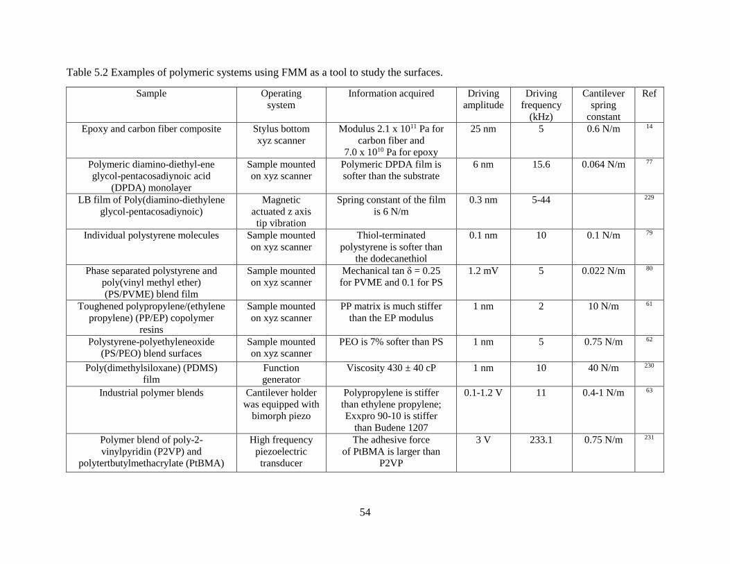
54
Table 5.2 Examples of polymeric systems using FMM as a tool to study the surfaces.
Sample
Operating
system
Information acquired Driving
amplitude
Driving
frequency
(kHz)
Cantilever
spring
constant
Ref
Epoxy and carbon fiber composite Stylus bottom
xyz scanner
Modulus 2.1 x 10¹¹ Pa for
carbon fiber and
7.0 x 10¹⁰ Pa for epoxy
25 nm 5 0.6 N/m 14
Polymeric diamino-diethyl-ene
glycol-pentacosadiynoic acid
(DPDA) monolayer
Sample mounted
on xyz scanner
Polymeric DPDA film is
softer than the substrate
6 nm 15.6 0.064 N/m 77
LB film of Poly(diamino-diethylene
glycol-pentacosadiynoic)
Magnetic
actuated z axis
tip vibration
Spring constant of the film
is 6 N/m
0.3 nm 5-44 229
Individual polystyrene molecules Sample mounted
on xyz scanner
Thiol-terminated
polystyrene is softer than
the dodecanethiol
0.1 nm 10 0.1 N/m 79
Phase separated polystyrene and
poly(vinyl methyl ether)
(PS/PVME) blend film
Sample mounted
on xyz scanner
Mechanical tan δ = 0.25
for PVME and 0.1 for PS
1.2 mV 5 0.022 N/m 80
Toughened polypropylene/(ethylene
propylene) (PP/EP) copolymer
resins
Sample mounted
on xyz scanner
PP matrix is much stiffer
than the EP modulus
1 nm 2 10 N/m 61
Polystyrene-polyethyleneoxide
(PS/PEO) blend surfaces
Sample mounted
on xyz scanner
PEO is 7% softer than PS 1 nm 5 0.75 N/m 62
Poly(dimethylsiloxane) (PDMS)
film
Function
generator
Viscosity 430 ± 40 cP 1 nm 10 40 N/m 230
Industrial polymer blends Cantilever holder
was equipped with
bimorph piezo
Polypropylene is stiffer
than ethylene propylene;
Exxpro 90-10 is stiffer
than Budene 1207
0.1-1.2 V 11 0.4-1 N/m 63
Polymer blend of poly-2-
vinylpyridin (P2VP) and
polytertbutylmethacrylate (PtBMA)
High frequency
piezoelectric
transducer
The adhesive force
of PtBMA is larger than
P2VP
3 V 233.1 0.75 N/m 231
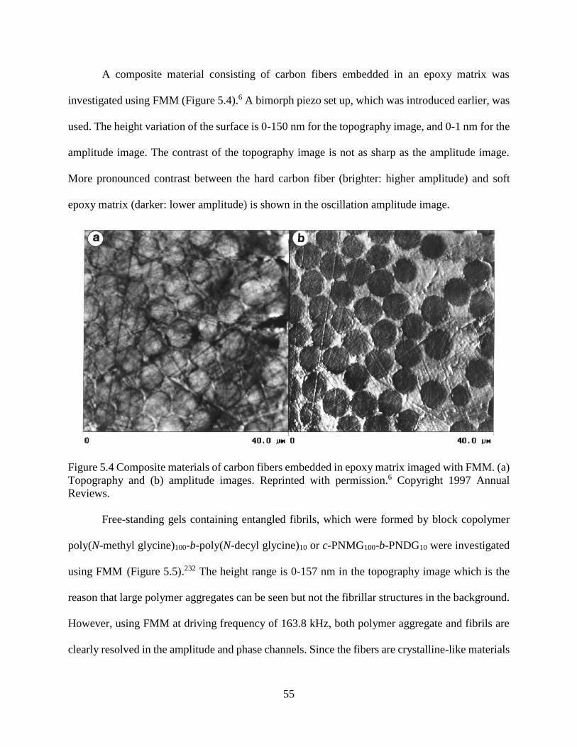
55
A composite material consisting of carbon fibers embedded in an epoxy matrix was
investigated using FMM (Figure 5.4).6 A bimorph piezo set up, which was introduced earlier, was
used. The height variation of the surface is 0-150 nm for the topography image, and 0-1 nm for the
amplitude image. The contrast of the topography image is not as sharp as the amplitude image.
More pronounced contrast between the hard carbon fiber (brighter: higher amplitude) and soft
epoxy matrix (darker: lower amplitude) is shown in the oscillation amplitude image.
Figure 5.4 Composite materials of carbon fibers embedded in epoxy matrix imaged with FMM. (a)
Topography and (b) amplitude images. Reprinted with permission.6 Copyright 1997 Annual
Reviews.
Free-standing gels containing entangled fibrils, which were formed by block copolymer
poly(N-methyl glycine)100-b-poly(N-decyl glycine)10 or c-PNMG100-b-PNDG10 were investigated
using FMM (Figure 5.5).232 The height range is 0-157 nm in the topography image which is the
reason that large polymer aggregates can be seen but not the fibrillar structures in the background.
However, using FMM at driving frequency of 163.8 kHz, both polymer aggregate and fibrils are
clearly resolved in the amplitude and phase channels. Since the fibers are crystalline-like materials
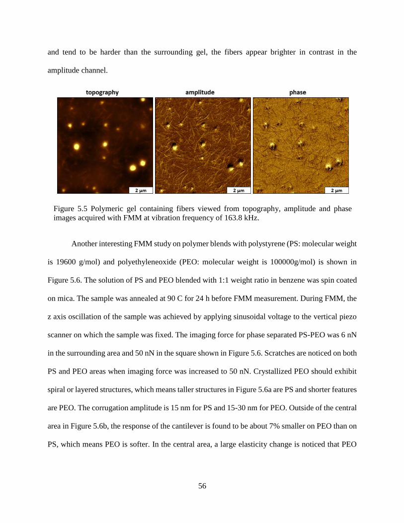
56
and tend to be harder than the surrounding gel, the fibers appear brighter in contrast in the
amplitude channel.
Another interesting FMM study on polymer blends with polystyrene (PS: molecular weight
is 19600 g/mol) and polyethyleneoxide (PEO: molecular weight is 100000g/mol) is shown in
Figure 5.6. The solution of PS and PEO blended with 1:1 weight ratio in benzene was spin coated
on mica. The sample was annealed at 90 C for 24 h before FMM measurement. During FMM, the
z axis oscillation of the sample was achieved by applying sinusoidal voltage to the vertical piezo
scanner on which the sample was fixed. The imaging force for phase separated PS-PEO was 6 nN
in the surrounding area and 50 nN in the square shown in Figure 5.6. Scratches are noticed on both
PS and PEO areas when imaging force was increased to 50 nN. Crystallized PEO should exhibit
spiral or layered structures, which means taller structures in Figure 5.6a are PS and shorter features
are PEO. The corrugation amplitude is 15 nm for PS and 15-30 nm for PEO. Outside of the central
area in Figure 5.6b, the response of the cantilever is found to be about 7% smaller on PEO than on
PS, which means PEO is softer. In the central area, a large elasticity change is noticed that PEO
Figure 5.5 Polymeric gel containing fibers viewed from topography, amplitude and phase
images acquired with FMM at vibration frequency of 163.8 kHz.
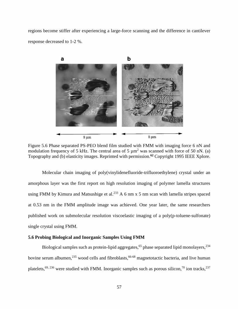
57
regions become stiffer after experiencing a large-force scanning and the difference in cantilever
response decreased to 1-2 %.
Figure 5.6 Phase separated PS-PEO blend film studied with FMM with imaging force 6 nN and
modulation frequency of 5 kHz. The central area of 5 µm2 was scanned with force of 50 nN. (a)
Topography and (b) elasticity images. Reprinted with permission.62 Copyright 1995 IEEE Xplore.
Molecular chain imaging of poly(vinylidenefluoride-trifluoroethylene) crystal under an
amorphous layer was the first report on high resolution imaging of polymer lamella structures
using FMM by Kimura and Matsushige et al.233 A 6 nm x 5 nm scan with lamella stripes spaced
at 0.53 nm in the FMM amplitude image was achieved. One year later, the same researchers
published work on submolecular resolution viscoelastic imaging of a poly(p-toluene-sulfonate)
single crystal using FMM.
5.6 Probing Biological and Inorganic Samples Using FMM
Biological samples such as protein-lipid aggregates,65 phase separated lipid monolayers,234
bovine serum albumen,235 wood cells and fibroblasts,66-68 magnetotactic bacteria, and live human
platelets,69, 236 were studied with FMM. Inorganic samples such as porous silicon,70 ion tracks,237
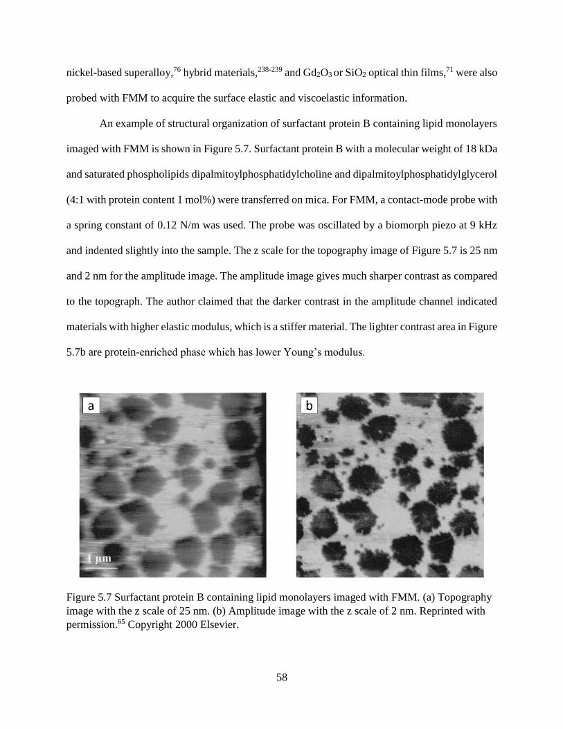
58
nickel-based superalloy,76 hybrid materials,238-239 and Gd2O3 or SiO2 optical thin films,71 were also
probed with FMM to acquire the surface elastic and viscoelastic information.
An example of structural organization of surfactant protein B containing lipid monolayers
imaged with FMM is shown in Figure 5.7. Surfactant protein B with a molecular weight of 18 kDa
and saturated phospholipids dipalmitoylphosphatidylcholine and dipalmitoylphosphatidylglycerol
(4:1 with protein content 1 mol%) were transferred on mica. For FMM, a contact-mode probe with
a spring constant of 0.12 N/m was used. The probe was oscillated by a biomorph piezo at 9 kHz
and indented slightly into the sample. The z scale for the topography image of Figure 5.7 is 25 nm
and 2 nm for the amplitude image. The amplitude image gives much sharper contrast as compared
to the topograph. The author claimed that the darker contrast in the amplitude channel indicated
materials with higher elastic modulus, which is a stiffer material. The lighter contrast area in Figure
5.7b are protein-enriched phase which has lower Young’s modulus.
Figure 5.7 Surfactant protein B containing lipid monolayers imaged with FMM. (a) Topography
image with the z scale of 25 nm. (b) Amplitude image with the z scale of 2 nm. Reprinted with
permission.65 Copyright 2000 Elsevier.
59
5.7 Conclusions
Force modulation microscopy is a powerful mode of AFM to acquire surface topography
and mechanical information simultaneously. Four FMM set-ups which were commonly used in
the literature were discussed in this review. Visualized AFM images containing the elastic and
viscoelastic differences about surface features can be shown in FMM amplitude and phase images.
Quantitative information such as Young’s modulus and elasticity can be calculated based on
amplitude channel of FMM. Application of FMM in self-assembled monolayer systems and
polymeric materials were summarized and discussed. The FMM mode was also applied in
inorganic and biological system to study the mechanical property of samples. Factors such as the
vibrational frequency, imaging media, and the shape and stiffness of the tip may influence the
contrast in FMM amplitude and phase images. However, it is possible to operate FMM in regions
that the image contrast reflects the relative elasticities of different components by tuning the
experimental conditions.
60
CHAPTER 6. SAMPLE STAGE DESIGNED FOR FORCE MODULATION
MICROSCOPY USING A TIP-MOUNTED AFM SCANNER
6.1 Introduction
Force modulation microscopy (FMM) can be used to identify and map differences in
stiffness or elasticity,79, 84 evaluate the composition of materials,85 and to study variations in
crystallinity,6 polymer phase separation, surface arrangement and distribution.80, 215-217 Materials
that have been studied with FMM include protein-lipid aggregates,65 patterned self-assembled
monolayers (SAMs),60 as well as polymer blends and resins.61-64 Molecularly resolved images of
polymer crystals have been acquired with FMM.233, 240 Quantitative measurements can be
evaluated using FMM for the Young’s modulus and the elasticity of samples. 75-76, 79, 213
For FMM mode the scanner is operated in contact-mode while the sample stage is driven
to vibrate. The AFM probe is scanned in continuous contact with the surface as the sample is
driven to vibrate at selected frequency and amplitude. Information of the topography, elastic
response and surface adhesion can be acquired concurrently. There are two instrument
configurations that have been used to accomplish FMM imaging, either the sample or tip can be
driven to vibrate with pressure applied at the area of tip-sample contact. Most commonly FMM
has been done using an instrument configuration with the sample placed directly on top of an xyz
scanner. Actuation of the z piezoelement causes the sample to vibrate for tip displacements of a
few nm in the z-direction.62, 77-80 Studies have been done using a cantilever holder equipped with
bimorph piezoelements to accomplish force modulation, which can actuate the tip as it is pressed
against the sample.63, 84 A magnetic field has been used to drive the vibration of a tip or tip-holder
assembly to accomplish force modulation imaging. 16, 85, 87 The driving frequency,225 imaging
media,89, 226 tip-sample contact area,221 amplitude of oscillation,227 and the shape and stiffness of
the tip72, 217 influence the resolution of FMM amplitude and phase images. A systematic study of
61
the factors which influence the contrast in FMM was previously reported by Jourdan, et al. for
nanopatterns inscribed within a film of organosilane.89
With the wide implementation of commercial scanning probe instruments designed to have
the tip mounted on the piezotube scanner, it would be practical to develop a sample stage to
facilitate sample modulation for FMM experiments. An accessory stage for FMM studies was
constructed with machined polycarbonate using an insulated coaxial cable connection to apply
current to an actuator element. The operation of the sample stage was evaluated by characterizing
three test samples with nanoscale dimensions. Test structures of nanoholes within a film of
octadecyltrichlorosiloxane (OTS) provide two distinct surface regions as the simplest platform for
FMM studies. Ring-shaped nanostructures prepared on Si(111) with 2-[methoxy
(polyethyleneoxy)propyl]trichlorosilane (PEG-silane) provide three domains for evaluating FMM
data. Finally, a complex sample consisting of a cyclic gel polymer of poly(N-methyl glycine)100-
b-poly(N-decyl glycine)10 containing fibrils was selected for FMM studies. Experiments were
accomplished in ambient conditions using conventional soft cantilevers.
6.2 Experimental Section
6.2.1 Materials and Reagents
Anhydrous toluene from Sigma-Aldrich (St. Louis, MO) was used as a solvent. Ethanol
used for cleaning samples was acquired from Pharmco-AAPER (Boucherville, Quebec).
Octadecyltrichlorosilane (OTS) and 2-[methoxy(polyethyleneoxy)propyl]trichlorosilane (PEG-
silane) were purchased from Gelest (Morrisville, PA) and used without further purification. Pieces
(5 × 7 mm) of polished Si(111) doped with boron (Ted Pella, Inc., Redding, CA) were used as
substrates for preparing nanopatterned films. Substrates were cleaned by immersion in piranha
solution for 1.5 h. Piranha solution is a mixture of sulfuric acid (Sigma-Aldrich) and hydrogen
peroxide (30%, Sigma-Aldrich) at a ratio of 3:1 (v/v). This solution is highly corrosive and should
62
be handled with caution. Silicon substrates were then rinsed copiously with water (Milli-Q,
Millipore, Bedford, MA) and dried with argon. Monodisperse polystyrene (496 ± 8.1 nm) and
silica (0.49 ± 0.02 μm) solutions were purchased from Duke Scientific (Palo Alto, CA). The
mesospheres were washed with deionized water by centrifugation to remove contaminants such as
charge stabilizers or surfactants. To prepare the cyclic gel sample for FMM, the polymer sample
was dissolved in methanol at 1% wt and formed a flow gel after 30 min. A drop of the flow gel
(10 μL) was deposited on a piece of freshly cleaved mica(0001), then dried in air before imaging
with FMM-AFM.
6.2.2 Atomic Force Microscopy
A Keysight model 5500 scanning probe microscope (SPM) equipped with a multipurpose
scanner was used for AFM characterizations (Keysight Technologies, Tempe, AZ). The scanner
has interchangeable nosecones for selected imaging modes. An empty plastic nosecone assembly
(the contact-mode nosecone) without metal components was used for force modulation
experiments. Silicon nitride cantilevers with an average force constant of 0.1 N m-1 were used for
FMM-AFM imaging (MSCT, Bruker, Camarillo, CA). Picoview v1.12 software was used for data
acquisition. Images were processed with Gwyddion (version 2.31) open software supported with
Czech Metrology Institute, which is freely available online.241
6.3 Results and Discussion
6.3.1 Design of the FMM Sample Stage
The sample stage was made with machined polycarbonate with a shape that was designed
for operation with a Keysight 5500 SPM. A photograph of the stage is shown in Figure 6.1,
indicating the location of the piezoactuator and the BNC cable connection. The essential
component of the FMM stage is the piezoactuator element (dimensions: 1 × 1 × 0.2 cm), which
enables a z-displacement of 2.2 μm in the range of 0-100 V input and has an axial resonance

63
frequency of 600 kHz (Physik Instrumente, Auburn, MA). For FMM studies, the voltages applied
to the piezoactuator ranged from 0.05-0.5 V. The black and red wires connect the piezoactuator
to the BNC cable which enables input of an AC signal to the stage to induce the vibration of the
piezoelement. With the Keysight 5500 instrument, a MAC box was used as an AC source by
connecting with the AAC output channel. There are three round flat magnets to attach the sample
stage to the scanner housing. Two alignment tracks were machined into the polycarbonate sample
holder for translating the sample stage in the x and y direction. A small magnet was embedded
within the center of the stage above the piezoactuator to attach samples. Samples for FMM studies
can either be magnetically clamped, taped or glued to the center of the stage. Further technical
details of the physical dimensions of the stage are provided in Appendix Figure D1.
Figure 6.1 Photograph of the polycarbonate FMM sample stage. The square piece at the
center of the stage is the piezoactuator, with a small circular magnet placed at the center for
attaching samples.

64
6.3.2 Characterization of Nanopatterns within an OTS Film using the FMM Sample Stage.
A test sample of OTS nanopatterns formed on Si(111) was used to evaluate the operation
and sensitivity of the FMM sample stage. Details of the procedure for preparing samples using
particle lithography with OTS were previously reported and are presented in Appendix Figure
D2.228 Experiments were designed to test the effect of turning the drive on or off as well as
evaluating changes in images for selected frequencies. Simultaneously acquired channels for
topography, amplitude, and phase are shown in Figure 6.2 for the sample of OTS nanopores. The
Figure 6.2 Sample of nanopores within a thin film of OTS characterized with the FMM sample
stage. (a) Images acquired at frequency of 18.8 kHz. (b) Image acquired with the drive turned
on or off at a frequency of 145.3 kHz. (c) Dynamic FMM study with ramping of the frequency
parameters during a single scan. The size of the images are 3 × 3 μm2.
65
same area was scanned using selected parameters for sample modulation. A hexagonal
arrangement of nanopores is visible in the topography frames, where the dark spots are areas of
uncovered substrate and the brighter areas are the matrix film of OTS. The distance between
adjacent nanopores measures 490 ± 44 nm. The depth and diameter of the nanopores measured 2.0
± 0.2 nm and 110 ± 10 nm respectively. Changes in the bright or dark contrast of the areas of the
nanopores are reversed for the amplitude versus phase channels in Figure 6.2a, when imaging at
frequency of 18.8 kHz. The bright or dark regions are highly sensitive to the driving frequency of
the sample stage. The phase images do not necessarily correlate with hardness of the samples.
When the drive is turned off, no features are distinguishable in amplitude and phase images as
demonstrated in Figure 6.2b. Note that by changing the frequency to 145.3 kHz the harder regions
of the substrate have bright contrast in both the amplitude and phase channels. In a dynamic FMM
study, the results of selectively ramping the frequency are displayed in Figure 6.2c without
interruption of data acquisition during a scan. The changes in color contrast for amplitude frames
can be interpreted by conducting a frequency sweep experiment, an example spectrum is shown in
Figure 6.3. The areas of the nanopores reveal exposed silicon substrate which is harder compared
with the surrounding film of OTS, thus greater amplitude or bright contrast is expected for
nanopore areas. However, the results shown in Figure 6.2c exhibit a reversal in contrast depending
sensitively on the frequency that was selected.
Clear differences in color contrast between areas of the nanopores and the matrix OTS
film are evident in the amplitude and phase images, however using these results to interpret the
hardness or softness of the areas can be complicated. For this example, the larger resonance peaks
at 18.8 and 145.3 kHz gave the predicted amplitude response showing bright dots for the locations
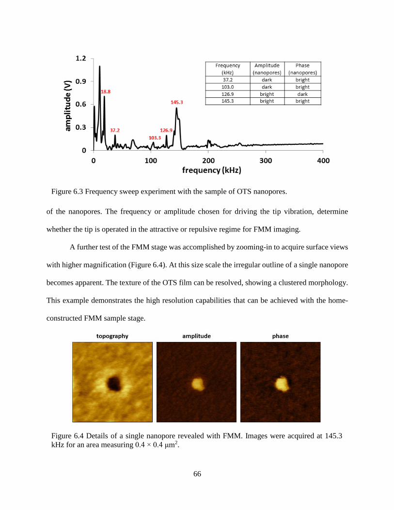
66
of the nanopores. The frequency or amplitude chosen for driving the tip vibration, determine
whether the tip is operated in the attractive or repulsive regime for FMM imaging.
A further test of the FMM stage was accomplished by zooming-in to acquire surface views
with higher magnification (Figure 6.4). At this size scale the irregular outline of a single nanopore
becomes apparent. The texture of the OTS film can be resolved, showing a clustered morphology.
This example demonstrates the high resolution capabilities that can be achieved with the home-
constructed FMM sample stage.
Figure 6.4 Details of a single nanopore revealed with FMM. Images were acquired at 145.3
kHz for an area measuring 0.4 × 0.4 μm2.
Figure 6.3 Frequency sweep experiment with the sample of OTS nanopores.
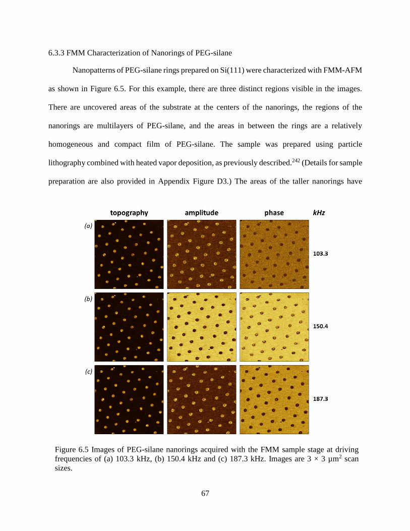
67
6.3.3 FMM Characterization of Nanorings of PEG-silane
Nanopatterns of PEG-silane rings prepared on Si(111) were characterized with FMM-AFM
as shown in Figure 6.5. For this example, there are three distinct regions visible in the images.
There are uncovered areas of the substrate at the centers of the nanorings, the regions of the
nanorings are multilayers of PEG-silane, and the areas in between the rings are a relatively
homogeneous and compact film of PEG-silane. The sample was prepared using particle
lithography combined with heated vapor deposition, as previously described.242 (Details for sample
preparation are also provided in Appendix Figure D3.) The areas of the taller nanorings have
Figure 6.5 Images of PEG-silane nanorings acquired with the FMM sample stage at driving
frequencies of (a) 103.3 kHz, (b) 150.4 kHz and (c) 187.3 kHz. Images are 3 × 3 µm2 scan
sizes.
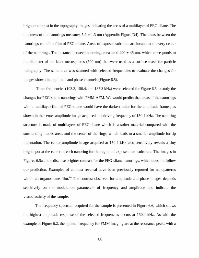
68
brighter contrast in the topography images indicating the areas of a multilayer of PEG-silane. The
thickness of the nanorings measures 5.9 ± 1.3 nm (Appendix Figure D4). The areas between the
nanorings contain a film of PEG-silane. Areas of exposed substrate are located at the very center
of the nanorings. The distance between nanorings measured 490 ± 45 nm, which corresponds to
the diameter of the latex mesospheres (500 nm) that were used as a surface mask for particle
lithography. The same area was scanned with selected frequencies to evaluate the changes for
images shown in amplitude and phase channels (Figure 6.5).
Three frequencies (103.3, 150.4, and 187.3 kHz) were selected for Figure 6.5 to study the
changes for PEG-silane nanorings with FMM-AFM. We would predict that areas of the nanorings
with a multilayer film of PEG-silane would have the darkest color for the amplitude frames, as
shown in the center amplitude image acquired at a driving frequency of 150.4 kHz. The nanoring
structure is made of multilayers of PEG-silane which is a softer material compared with the
surrounding matrix areas and the center of the rings, which leads to a smaller amplitude for tip
indentation. The center amplitude image acquired at 150.4 kHz also sensitively reveals a tiny
bright spot at the center of each nanoring for the region of exposed hard substrate. The images in
Figures 6.5a and c disclose brighter contrast for the PEG-silane nanorings, which does not follow
our prediction. Examples of contrast reversal have been previously reported for nanopatterns
within an organosilane film.89 The contrast observed for amplitude and phase images depends
sensitively on the modulation parameters of frequency and amplitude and indicate the
viscoelasticity of the sample.
The frequency spectrum acquired for the sample is presented in Figure 6.6, which shows
the highest amplitude response of the selected frequencies occurs at 150.4 kHz. As with the
example of Figure 6.2, the optimal frequency for FMM imaging are at the resonance peaks with a
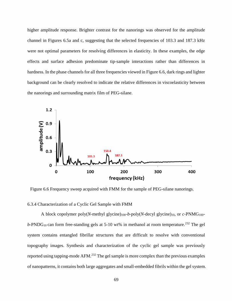
69
higher amplitude response. Brighter contrast for the nanorings was observed for the amplitude
channel in Figures 6.5a and c, suggesting that the selected frequencies of 103.3 and 187.3 kHz
were not optimal parameters for resolving differences in elasticity. In these examples, the edge
effects and surface adhesion predominate tip-sample interactions rather than differences in
hardness. In the phase channels for all three frequencies viewed in Figure 6.6, dark rings and lighter
background can be clearly resolved to indicate the relative differences in viscoelasticity between
the nanorings and surrounding matrix film of PEG-silane.
6.3.4 Characterization of a Cyclic Gel Sample with FMM
A block copolymer poly(N-methyl glycine)100-b-poly(N-decyl glycine)10, or c-PNMG100-
b-PNDG10 can form free-standing gels at 5-10 wt% in methanol at room temperature.232 The gel
system contains entangled fibrillar structures that are difficult to resolve with conventional
topography images. Synthesis and characterization of the cyclic gel sample was previously
reported using tapping-mode AFM.232 The gel sample is more complex than the previous examples
of nanopatterns, it contains both large aggregates and small-embedded fibrils within the gel system.
Figure 6.6 Frequency sweep acquired with FMM for the sample of PEG-silane nanorings.
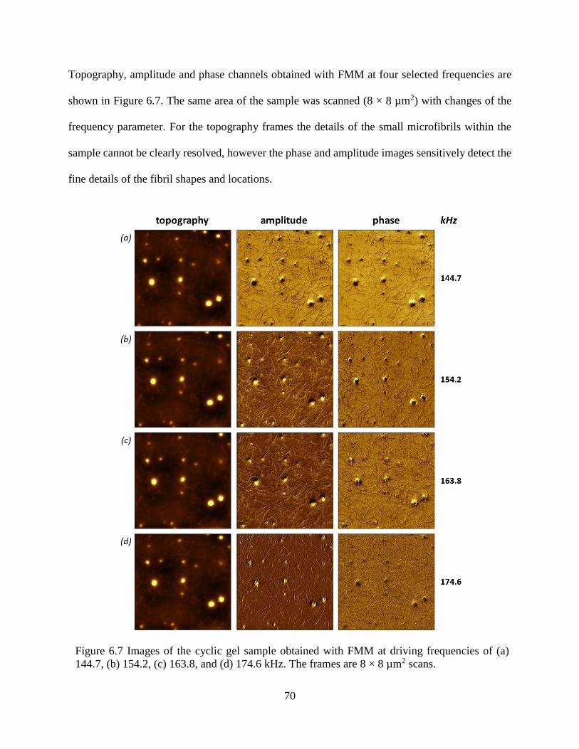
70
Topography, amplitude and phase channels obtained with FMM at four selected frequencies are
shown in Figure 6.7. The same area of the sample was scanned (8 × 8 µm2) with changes of the
frequency parameter. For the topography frames the details of the small microfibrils within the
sample cannot be clearly resolved, however the phase and amplitude images sensitively detect the
fine details of the fibril shapes and locations.
Figure 6.7 Images of the cyclic gel sample obtained with FMM at driving frequencies of (a)
144.7, (b) 154.2, (c) 163.8, and (d) 174.6 kHz. The frames are 8 × 8 µm2 scans.
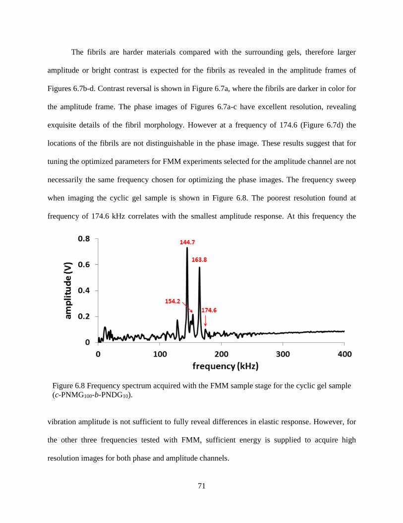
71
The fibrils are harder materials compared with the surrounding gels, therefore larger
amplitude or bright contrast is expected for the fibrils as revealed in the amplitude frames of
Figures 6.7b-d. Contrast reversal is shown in Figure 6.7a, where the fibrils are darker in color for
the amplitude frame. The phase images of Figures 6.7a-c have excellent resolution, revealing
exquisite details of the fibril morphology. However at a frequency of 174.6 (Figure 6.7d) the
locations of the fibrils are not distinguishable in the phase image. These results suggest that for
tuning the optimized parameters for FMM experiments selected for the amplitude channel are not
necessarily the same frequency chosen for optimizing the phase images. The frequency sweep
when imaging the cyclic gel sample is shown in Figure 6.8. The poorest resolution found at
frequency of 174.6 kHz correlates with the smallest amplitude response. At this frequency the
vibration amplitude is not sufficient to fully reveal differences in elastic response. However, for
the other three frequencies tested with FMM, sufficient energy is supplied to acquire high
resolution images for both phase and amplitude channels.
Figure 6.8 Frequency spectrum acquired with the FMM sample stage for the cyclic gel sample
(c-PNMG100-b-PNDG10).
72
Both the driving frequency and the amplitude of the resonance peak determine the
resolution of the FMM amplitude and phase channels. Weaker resonance peaks were shown to
display a contrast reversal for elastic response. For the sample of OTS nanopores and the nanorings
of PEG-silane, strong resonance peaks were found at frequencies below 25 kHz. The voltages
applied to the piezoactuator of the stage were 0.4 V for the OTS nanopores and 0.5 V for PEG-
silane nanorings. For the nanopatterned surfaces of OTS and PEG-silane the overall z scale
measured less than 10 nm, while the cyclic gel sample had taller features of 160 nm (Appendix
Figure D5). For the complicated system of the cyclic gel sample, which has larger aggregates along
with micron-sized fibrils embedded in the gel system, stronger resonance peaks were detected in
the frequency range of 120-180 kHz using 0.05 V applied to the piezoactuator.
6.4 Conclusions
Excellent resolution can be achieved when using the home-constructed FMM sample stage
with a tip-mounted scanner, even for complex surfaces or multi-component samples. The FMM
stage is suitable for imaging samples in ambient conditions and exhibited high resolution when
experimental parameters were optimized. Interpretation of FMM amplitude frames is complicated
for acquiring quantitative measurements of elastic response, the parameters for driving frequency
and amplitude require optimization. Knowledge of the sample composition is critical for correctly
interpreting information from amplitude images. Future studies will incorporate a liquid cell for
the design of the FMM stage to enable FMM characterizations in liquids. Machined glass
components will be used for constructing a sample stage to enable studies in solvents.

73
CHAPTER 7: DIRECT COMPARISON OF SAMPLE ACTUATION VERSUS TIP
VIBRATION CONFIGURATION FOR FORCE MODULATION AFM
7.1 Introduction
Force modulation microscopy (FMM) was invented in 1991 and has since been used by
researchers in many fields.14, 77, 79-80, 82, 215, 220, 235 This mode of atomic force microscopy (AFM) is
used to measure the dynamic response of the sample while applying pressure to the surface during
contact-mode imaging, providing elasticity and viscoelasticity measurements of the sample.81 The
most common instrument set up is to mount the sample on a piezoelectric xyz scanner and apply
a sinusoidal voltage to the vertical piezoceramic material, which will cause the sample to vibrate
in the z direction.62, 77-81 Another common setup for FMM is to use a cantilever holder equipped
with bimorph piezo.63, 83-84 The bimorph piezo oscillates the cantilever near its resonance frequency
during tapping and slightly presses the tip into the sample during force modulation. Therefore,
tapping-mode and force modulation images can be acquired using this design. Mechanical
vibration is not the only way to modulate the tip or sample for FMM. In some cases, a solenoid is
placed around the scanner tube, where the sample is attached, to generate an oscillating magnetic
field. A magnetically coated cantilever or a small spherical magnetic particle glued to the back of
the cantilever can be indirectly modulated by the oscillation of the magnetic field.85, 87-88, 213
Force modulation microscopy is able to acquire topographical information along with the
mechanical properties (elasticity and viscoelasticity) of samples at the same time.6 It has great
applications in a variety of fields, especially soft materials such as polymers and biological
systems.63, 236 Polymeric systems such as toughened polypropylene resins,61 polystyrene-
polyethyleneoxide and polyvinyl chloride-polycarbonate blends62, 64 have been probed with FMM
for viscoelastic information.209, 230 Biological systems such as magnetotactic bacteria,69 human
platelets,69 living fibroblasts67-68 have been investigated for elastic properties using FMM.65-66
74
Other systems such as hybrid materials,238-239 patterned or phase separated self-assembled
monolayers,60, 216 Gd2O3 or SiO2 optical thin films,71 have also been studied with FMM.70, 237
Our group has developed two methods for investigating the mechanical properties of
samples. We have recently designed a sample stage capable of sample modulated FMM. Several
samples have been evaluated to test the abilities of this stage. This polycarbonate sample stage can
be easily reshaped to fit other models of AFM. Indirect magnetic modulation (IMM), which
invented in our group earlier, is an alternative way to do force modulation microscopy by indirectly
modulating the nosecone assembly.16 The soft, nonmagnetic cantilever is driven to vibrate with
the motion of the nosecone containing ferromagnetic materials. The nosecone is induced to vibrate
with the flux of an external electromagnetic field, which is generated by the solenoid beneath the
MAC-mode sample stage. The goal of this study is to use nanoring patterns of 4-
(chloromethyl)phenyltrichlorosilane (CMPS) as a test platform to compare FMM using the newly-
designed sample stage and IMM using the MAC-mode stage. The organosilane, CMPS, is highly
reactive to itself and easily forms multilayers on surfaces. The multilayers provide soft surfaces
suitable for force modulation studies. In addition, four regions (CMPS monolayer, multilayers and
hard surfaces) are formed by patterning CMPS with particle lithography, which makes this sample
a good candidate for elasticity studies on surfaces. Additionally, the influence of driving frequency
and vibration amplitude on FMM and IMM imaging are systematically studied in this Chapter for
the very first time.
7.2 Experiment Section
7.2.1 Materials and Reagents
Single-side polished Si(111) doped with boron (Ted Pella, Inc., Redding, CA) was used as
substrates. Monodisperse latex mesoparticles (496 ± 8.1 nm) were purchased from Duke Scientific
(Palo Alto, CA). Nanopatterns were fabricated using 4-(chloromethyl)phenyltrichlorosilane
75
(Gelest, Morrisville, PA) without further purification. Toluene, sulfuric acid, and hydrogen
peroxide (30%) were obtained from Sigma-Aldrich (St. Louis, MO). Ethanol was used to clean
the substrate, which was purchased from Pharmco-AAPER (Boucherville, Quebec).
7.2.2 Atomic Force Microscopy
A Keysight 5500 SPM (Keysight Technologies, Tempe, AZ) was used for FMM and IMM
studies. The scanner can incorporate interchangeable nosecones for selected imaging modes. A
contact-mode nosecone assembly without metal components was used for the FMM study. An
AAC nosecone, which has two metal pins, was used for the IMM study. Picoview v1.12 software
was used for data acquisition. Images were processed with Gwyddion (version 2.31) open software
supported with Czech Metrology Institute, which is freely available online.241 A nonmagnetic
silicon nitride probe with force constant of 0.1 N m-1 was used for FMM and IMM imaging (MSCT,
Bruker, Camarillo, CA).
7.2.3 Preparation of CMPS Nanorings
The Si(111) substrates were immersed in piranha solution for 2 h to remove organic
contaminants. Piranha solution is a mixture of sulfuric acid and hydrogen peroxide at a ratio of 3:1
(v/v). This solution is highly corrosive and should be handled carefully. Substrates were then
rinsed with copious of water (Milli-Q, Millipore, Bedford, MA) and dried with argon. The
mesospheres were washed three times with deionized water to remove charge stabilizers and
surfactants. Immediately after drying the substrate, 10 µL of the latex mesosphere suspension was
deposited. The sample was dried in air for 4 h to produce surface masks. Next, the sample was
placed in a sealed cup containing 300 μL of neat CMPS silane. The cup was placed in an oven at
70 C for 18 h. The CMPS silane was vaporized to react with Si substrate where the mesospheres
do not contact the substrate. After cooling, the sample was rinsed with water and toluene. To
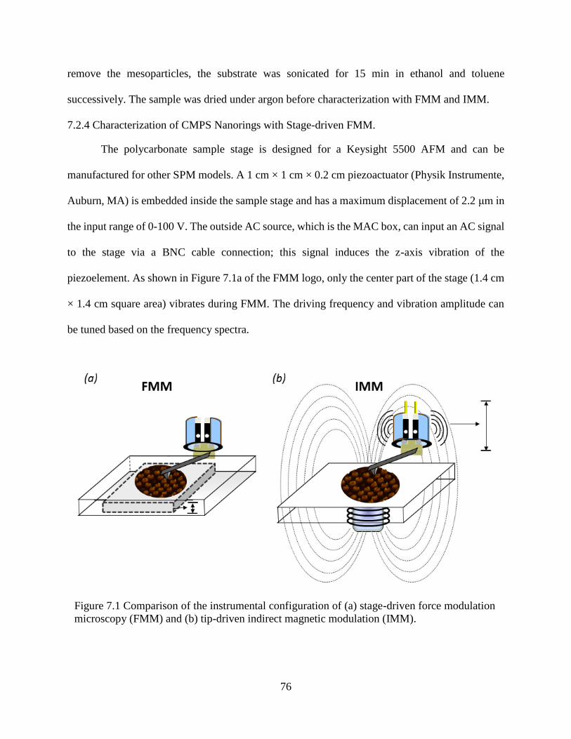
76
remove the mesoparticles, the substrate was sonicated for 15 min in ethanol and toluene
successively. The sample was dried under argon before characterization with FMM and IMM.
7.2.4 Characterization of CMPS Nanorings with Stage-driven FMM.
The polycarbonate sample stage is designed for a Keysight 5500 AFM and can be
manufactured for other SPM models. A 1 cm × 1 cm × 0.2 cm piezoactuator (Physik Instrumente,
Auburn, MA) is embedded inside the sample stage and has a maximum displacement of 2.2 μm in
the input range of 0-100 V. The outside AC source, which is the MAC box, can input an AC signal
to the stage via a BNC cable connection; this signal induces the z-axis vibration of the
piezoelement. As shown in Figure 7.1a of the FMM logo, only the center part of the stage (1.4 cm
× 1.4 cm square area) vibrates during FMM. The driving frequency and vibration amplitude can
be tuned based on the frequency spectra.
Figure 7.1 Comparison of the instrumental configuration of (a) stage-driven force modulation
microscopy (FMM) and (b) tip-driven indirect magnetic modulation (IMM).
77
7.2.5 Characterization of CMPS Nanorings with Tip-driven IMM
The invention of IMM mode was introduced by our group previously.16 The entire tip
holder assembly is indirectly modulated through the flux of an external ac electromagnetic field
generated with a wire coil solenoid located underneath the sample stage Figure 7.1b (IMM logo).
The metal pins inside the nosecone are vibrating in the magnetic field to indirectly vibrate the
AFM tip.
Both stage-driven FMM and tip driven IMM are operated in contact-mode. Height
(topography channel), elasticity (amplitude channel), and viscosity/viscoelasticity (phase channel)
information can be acquired at the same time. Tips with a low spring constant (< 1 N m-1) are
suggested for use with both methods.
7.3 Results
7.3.1 Nanorings of CMPS Studied with FMM and IMM with and without Sample/Tip
Modulation
The shape and hexagonal pattern of CMPS nanorings on a silicon surface prepared by
particle lithography combined with chemical vapor deposition can be viewed in Figure 7.2. The
periodicity of the CMPS nanopatterns is ~500 nm, which is determined by the diameter of the latex
mesospheres used to fabricate the patterned sample. The shapes of the nanorings are not identical
due to a variation in the volume of water at the meniscus of the mesospheres which affects the
polymerization reaction of CMP. Brighter contrast in the topograph corresponds to the
polymerized CMPS nanorings, while the darker background consists of a CMPS monolayer or
nanopillars in between the nanorings. Individual dark points can be viewed in the amplitude image
in the areas between nanorings, which is CMPS nanopillars (several layers of CMPS). The centers
of the nanorings are the bare silicon substrates, which are the lowest point on the surface.
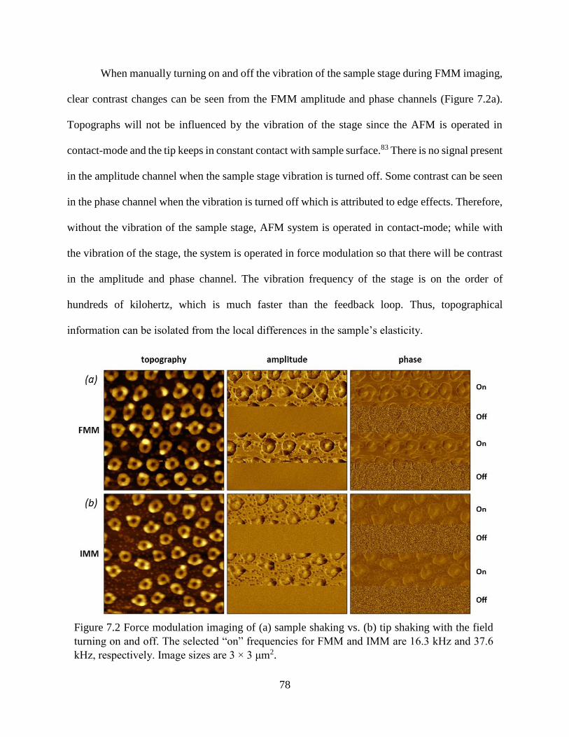
78
When manually turning on and off the vibration of the sample stage during FMM imaging,
clear contrast changes can be seen from the FMM amplitude and phase channels (Figure 7.2a).
Topographs will not be influenced by the vibration of the stage since the AFM is operated in
contact-mode and the tip keeps in constant contact with sample surface.83 There is no signal present
in the amplitude channel when the sample stage vibration is turned off. Some contrast can be seen
in the phase channel when the vibration is turned off which is attributed to edge effects. Therefore,
without the vibration of the sample stage, AFM system is operated in contact-mode; while with
the vibration of the stage, the system is operated in force modulation so that there will be contrast
in the amplitude and phase channel. The vibration frequency of the stage is on the order of
hundreds of kilohertz, which is much faster than the feedback loop. Thus, topographical
information can be isolated from the local differences in the sample’s elasticity.
Figure 7.2 Force modulation imaging of (a) sample shaking vs. (b) tip shaking with the field
turning on and off. The selected “on” frequencies for FMM and IMM are 16.3 kHz and 37.6
kHz, respectively. Image sizes are 3 × 3 μm2.
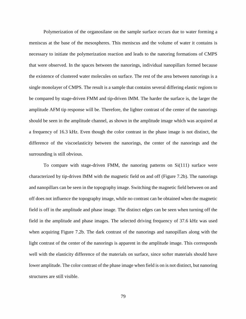
79
Polymerization of the organosilane on the sample surface occurs due to water forming a
meniscus at the base of the mesospheres. This meniscus and the volume of water it contains is
necessary to initiate the polymerization reaction and leads to the nanoring formations of CMPS
that were observed. In the spaces between the nanorings, individual nanopillars formed because
the existence of clustered water molecules on surface. The rest of the area between nanorings is a
single monolayer of CMPS. The result is a sample that contains several differing elastic regions to
be compared by stage-driven FMM and tip-driven IMM. The harder the surface is, the larger the
amplitude AFM tip response will be. Therefore, the lighter contrast of the center of the nanorings
should be seen in the amplitude channel, as shown in the amplitude image which was acquired at
a frequency of 16.3 kHz. Even though the color contrast in the phase image is not distinct, the
difference of the viscoelasticity between the nanorings, the center of the nanorings and the
surrounding is still obvious.
To compare with stage-driven FMM, the nanoring patterns on Si(111) surface were
characterized by tip-driven IMM with the magnetic field on and off (Figure 7.2b). The nanorings
and nanopillars can be seen in the topography image. Switching the magnetic field between on and
off does not influence the topography image, while no contrast can be obtained when the magnetic
field is off in the amplitude and phase image. The distinct edges can be seen when turning off the
field in the amplitude and phase images. The selected driving frequency of 37.6 kHz was used
when acquiring Figure 7.2b. The dark contrast of the nanorings and nanopillars along with the
light contrast of the center of the nanorings is apparent in the amplitude image. This corresponds
well with the elasticity difference of the materials on surface, since softer materials should have
lower amplitude. The color contrast of the phase image when field is on is not distinct, but nanoring
structures are still visible.
80
Nanorings of CMPS studied with stage-driven FMM and tip-driven IMM with and without
sample/tip modulation have similar results. High resolution AFM images with elasticity
information can be acquired for both methods when same amount of voltage was applied to the
system (0.8 V).
7.3.2 Nanorings of CMPS Studied with FMM at Selected Driving Frequencies
The frequency-dependence of the tip response to the CMPS nanorings is shown in Figure
7.3. The same area was scanned five times at selected driving frequencies (Figures 7.3a-e). The
color scales for the topography frames of Figures 7.3a-e for the height differences remain the same
regardless the frequency used. Light contrast of the nanorings and dark contrast of the centers of
nanorings in the amplitude frame can be seen at driving frequencies of 35.2, 95.6, and 152.4 kHz
(Figures 7.3c-e). Dark nanorings and light center can be viewed in the amplitude channel at a
frequency of 16.3 kHz (Figure 7.3b). The contrast at a frequency of 11.5 kHz is not distinct, but
the shape still can be seen with clear edges of the nanorings (Figure 7.3a). The viscoelasticity
difference of the sample surface can be viewed clearly in the phase frames of Figures 7.3a-c and
e, but not d. A clear contrast difference between center of the nanoring (bare substrate) and the
surrounding area (CMPS monolayer) can be seen from amplitude channels b, c, and d, and phase
channels a, b, c, and e.
In the amplitude channel, the harder material should have a lighter contrast. This means
that a frequency of 16.3 kHz is the most representative frequency to show the mechanical
differences of the CMPS nanoring sample.
7.3.3 Nanorings of CMPS Studied with IMM at Selected Driving Frequencies
Five driving frequencies of 37.6, 54.6, 76.8, 144.1 and 163.1 kHz were selected based upon
the frequency sweep, which will be shown later, to investigate the frequency-dependence of this
sample using tip-driven IMM. The same area was scanned five times at selected frequencies as
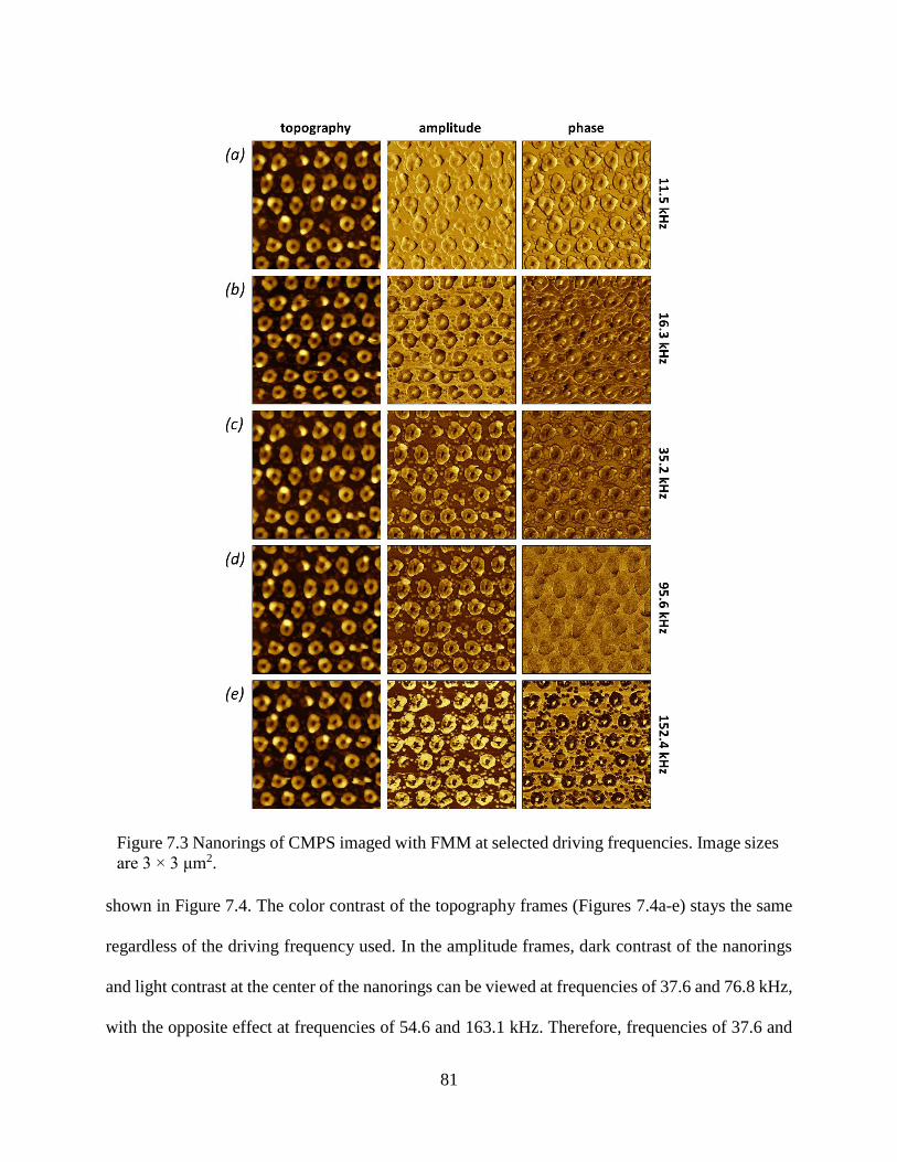
81
shown in Figure 7.4. The color contrast of the topography frames (Figures 7.4a-e) stays the same
regardless of the driving frequency used. In the amplitude frames, dark contrast of the nanorings
and light contrast at the center of the nanorings can be viewed at frequencies of 37.6 and 76.8 kHz,
with the opposite effect at frequencies of 54.6 and 163.1 kHz. Therefore, frequencies of 37.6 and
Figure 7.3 Nanorings of CMPS imaged with FMM at selected driving frequencies. Image sizes
are 3 × 3 μm2.
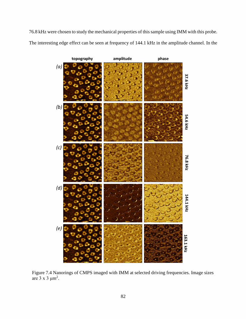
82
76.8 kHz were chosen to study the mechanical properties of this sample using IMM with this probe.
The interesting edge effect can be seen at frequency of 144.1 kHz in the amplitude channel. In the
Figure 7.4 Nanorings of CMPS imaged with IMM at selected driving frequencies. Image sizes
are 3 x 3 μm2.
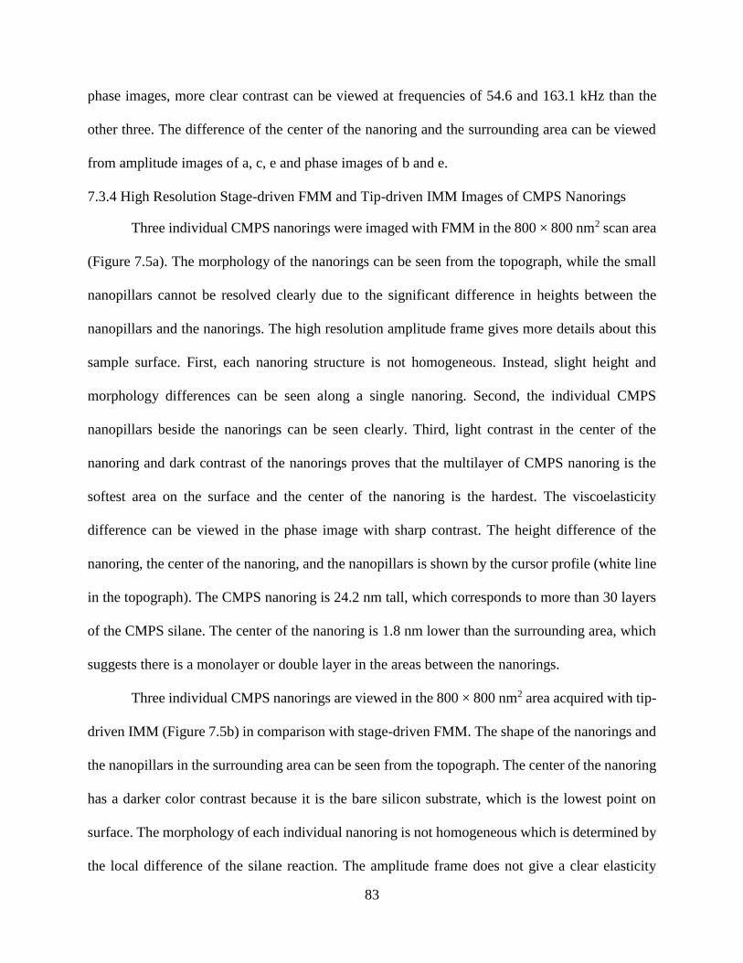
83
phase images, more clear contrast can be viewed at frequencies of 54.6 and 163.1 kHz than the
other three. The difference of the center of the nanoring and the surrounding area can be viewed
from amplitude images of a, c, e and phase images of b and e.
7.3.4 High Resolution Stage-driven FMM and Tip-driven IMM Images of CMPS Nanorings
Three individual CMPS nanorings were imaged with FMM in the 800 × 800 nm2 scan area
(Figure 7.5a). The morphology of the nanorings can be seen from the topograph, while the small
nanopillars cannot be resolved clearly due to the significant difference in heights between the
nanopillars and the nanorings. The high resolution amplitude frame gives more details about this
sample surface. First, each nanoring structure is not homogeneous. Instead, slight height and
morphology differences can be seen along a single nanoring. Second, the individual CMPS
nanopillars beside the nanorings can be seen clearly. Third, light contrast in the center of the
nanoring and dark contrast of the nanorings proves that the multilayer of CMPS nanoring is the
softest area on the surface and the center of the nanoring is the hardest. The viscoelasticity
difference can be viewed in the phase image with sharp contrast. The height difference of the
nanoring, the center of the nanoring, and the nanopillars is shown by the cursor profile (white line
in the topograph). The CMPS nanoring is 24.2 nm tall, which corresponds to more than 30 layers
of the CMPS silane. The center of the nanoring is 1.8 nm lower than the surrounding area, which
suggests there is a monolayer or double layer in the areas between the nanorings.
Three individual CMPS nanorings are viewed in the 800 × 800 nm2 area acquired with tip-
driven IMM (Figure 7.5b) in comparison with stage-driven FMM. The shape of the nanorings and
the nanopillars in the surrounding area can be seen from the topograph. The center of the nanoring
has a darker color contrast because it is the bare silicon substrate, which is the lowest point on
surface. The morphology of each individual nanoring is not homogeneous which is determined by
the local difference of the silane reaction. The amplitude frame does not give a clear elasticity
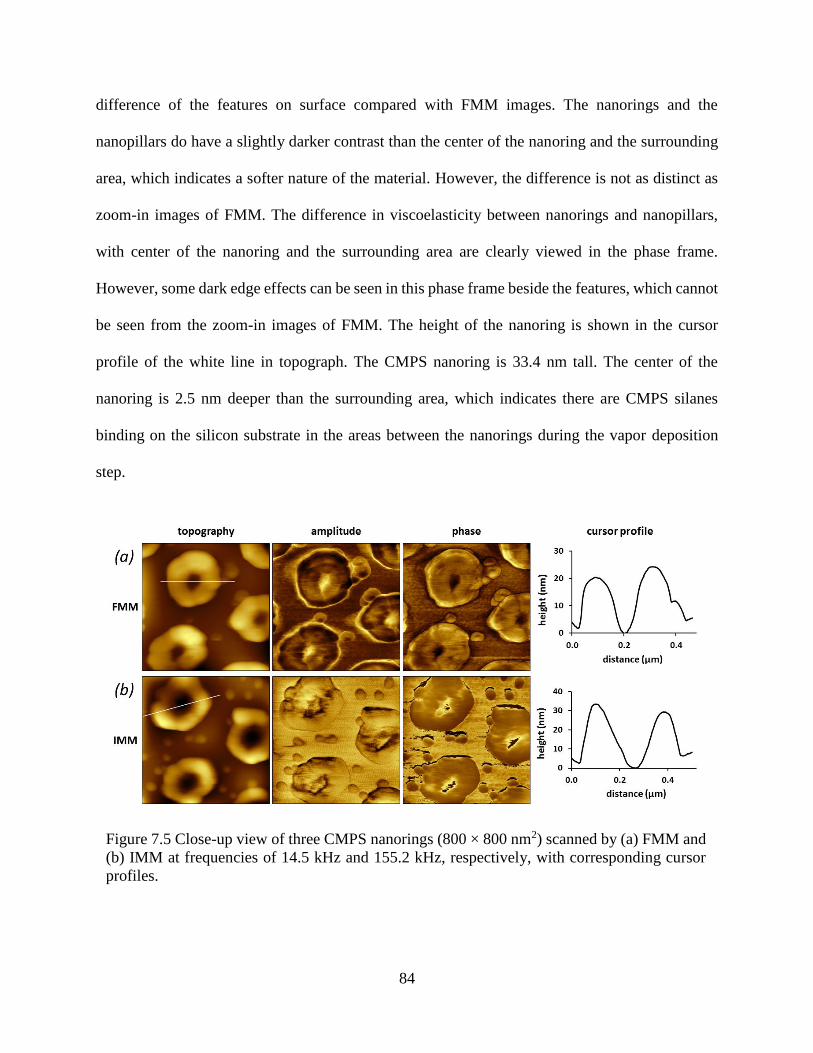
84
difference of the features on surface compared with FMM images. The nanorings and the
nanopillars do have a slightly darker contrast than the center of the nanoring and the surrounding
area, which indicates a softer nature of the material. However, the difference is not as distinct as
zoom-in images of FMM. The difference in viscoelasticity between nanorings and nanopillars,
with center of the nanoring and the surrounding area are clearly viewed in the phase frame.
However, some dark edge effects can be seen in this phase frame beside the features, which cannot
be seen from the zoom-in images of FMM. The height of the nanoring is shown in the cursor
profile of the white line in topograph. The CMPS nanoring is 33.4 nm tall. The center of the
nanoring is 2.5 nm deeper than the surrounding area, which indicates there are CMPS silanes
binding on the silicon substrate in the areas between the nanorings during the vapor deposition
step.
Figure 7.5 Close-up view of three CMPS nanorings (800 × 800 nm2) scanned by (a) FMM and
(b) IMM at frequencies of 14.5 kHz and 155.2 kHz, respectively, with corresponding cursor
profiles.
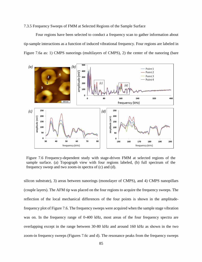
85
7.3.5 Frequency Sweeps of FMM at Selected Regions of the Sample Surface
Four regions have been selected to conduct a frequency scan to gather information about
tip-sample interactions as a function of induced vibrational frequency. Four regions are labeled in
Figure 7.6a as: 1) CMPS nanorings (multilayers of CMPS), 2) the center of the nanoring (bare
silicon substrate), 3) areas between nanorings (monolayer of CMPS), and 4) CMPS nanopillars
(couple layers). The AFM tip was placed on the four regions to acquire the frequency sweeps. The
reflection of the local mechanical differences of the four points is shown in the amplitude-
frequency plot of Figure 7.6. The frequency sweeps were acquired when the sample stage vibration
was on. In the frequency range of 0-400 kHz, most areas of the four frequency spectra are
overlapping except in the range between 30-80 kHz and around 160 kHz as shown in the two
zoom-in frequency sweeps (Figures 7.6c and d). The resonance peaks from the frequency sweeps
Figure 7.6 Frequency-dependent study with stage-driven FMM at selected regions of the
sample surface. (a) Topograph view with four regions labeled, (b) full spectrum of the
frequency sweep and two zoom-in spectra of (c) and (d).
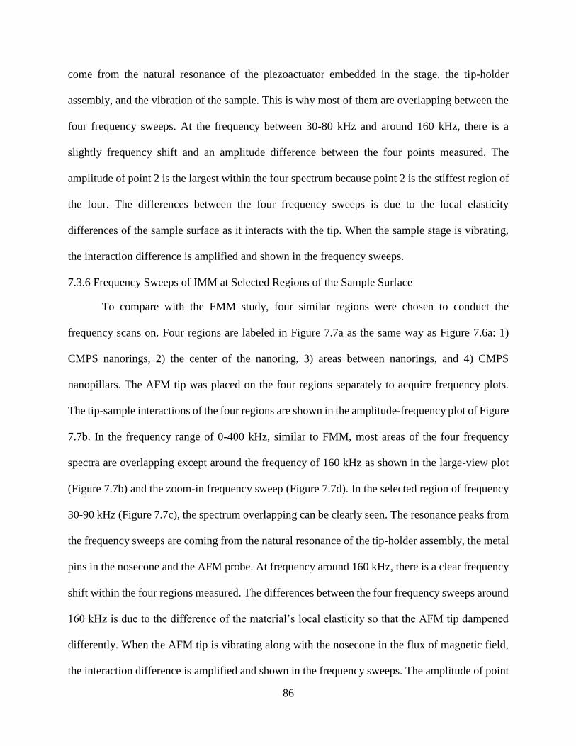
86
come from the natural resonance of the piezoactuator embedded in the stage, the tip-holder
assembly, and the vibration of the sample. This is why most of them are overlapping between the
four frequency sweeps. At the frequency between 30-80 kHz and around 160 kHz, there is a
slightly frequency shift and an amplitude difference between the four points measured. The
amplitude of point 2 is the largest within the four spectrum because point 2 is the stiffest region of
the four. The differences between the four frequency sweeps is due to the local elasticity
differences of the sample surface as it interacts with the tip. When the sample stage is vibrating,
the interaction difference is amplified and shown in the frequency sweeps.
7.3.6 Frequency Sweeps of IMM at Selected Regions of the Sample Surface
To compare with the FMM study, four similar regions were chosen to conduct the
frequency scans on. Four regions are labeled in Figure 7.7a as the same way as Figure 7.6a: 1)
CMPS nanorings, 2) the center of the nanoring, 3) areas between nanorings, and 4) CMPS
nanopillars. The AFM tip was placed on the four regions separately to acquire frequency plots.
The tip-sample interactions of the four regions are shown in the amplitude-frequency plot of Figure
7.7b. In the frequency range of 0-400 kHz, similar to FMM, most areas of the four frequency
spectra are overlapping except around the frequency of 160 kHz as shown in the large-view plot
(Figure 7.7b) and the zoom-in frequency sweep (Figure 7.7d). In the selected region of frequency
30-90 kHz (Figure 7.7c), the spectrum overlapping can be clearly seen. The resonance peaks from
the frequency sweeps are coming from the natural resonance of the tip-holder assembly, the metal
pins in the nosecone and the AFM probe. At frequency around 160 kHz, there is a clear frequency
shift within the four regions measured. The differences between the four frequency sweeps around
160 kHz is due to the difference of the material’s local elasticity so that the AFM tip dampened
differently. When the AFM tip is vibrating along with the nosecone in the flux of magnetic field,
the interaction difference is amplified and shown in the frequency sweeps. The amplitude of point
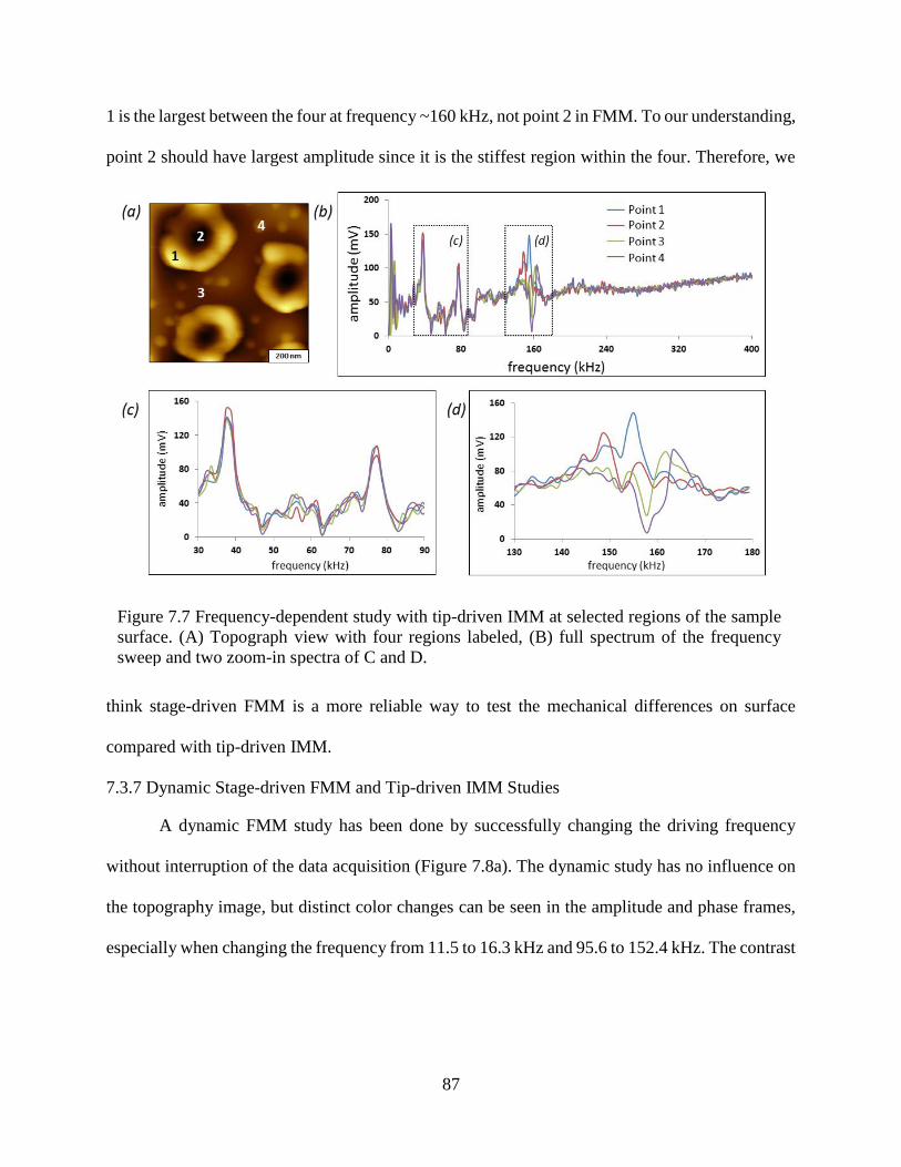
87
1 is the largest between the four at frequency ~160 kHz, not point 2 in FMM. To our understanding,
point 2 should have largest amplitude since it is the stiffest region within the four. Therefore, we
think stage-driven FMM is a more reliable way to test the mechanical differences on surface
compared with tip-driven IMM.
7.3.7 Dynamic Stage-driven FMM and Tip-driven IMM Studies
A dynamic FMM study has been done by successfully changing the driving frequency
without interruption of the data acquisition (Figure 7.8a). The dynamic study has no influence on
the topography image, but distinct color changes can be seen in the amplitude and phase frames,
especially when changing the frequency from 11.5 to 16.3 kHz and 95.6 to 152.4 kHz. The contrast
Figure 7.7 Frequency-dependent study with tip-driven IMM at selected regions of the sample
surface. (A) Topograph view with four regions labeled, (B) full spectrum of the frequency
sweep and two zoom-in spectra of C and D.
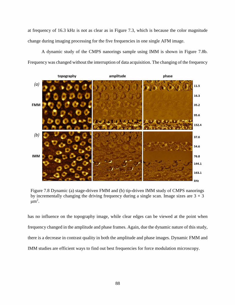
88
at frequency of 16.3 kHz is not as clear as in Figure 7.3, which is because the color magnitude
change during imaging processing for the five frequencies in one single AFM image.
A dynamic study of the CMPS nanorings sample using IMM is shown in Figure 7.8b.
Frequency was changed without the interruption of data acquisition. The changing of the frequency
has no influence on the topography image, while clear edges can be viewed at the point when
frequency changed in the amplitude and phase frames. Again, due the dynamic nature of this study,
there is a decrease in contrast quality in both the amplitude and phase images. Dynamic FMM and
IMM studies are efficient ways to find out best frequencies for force modulation microscopy.
Figure 7.8 Dynamic (a) stage-driven FMM and (b) tip-driven IMM study of CMPS nanorings
by incrementally changing the driving frequency during a single scan. Image sizes are 3 × 3
μm2.
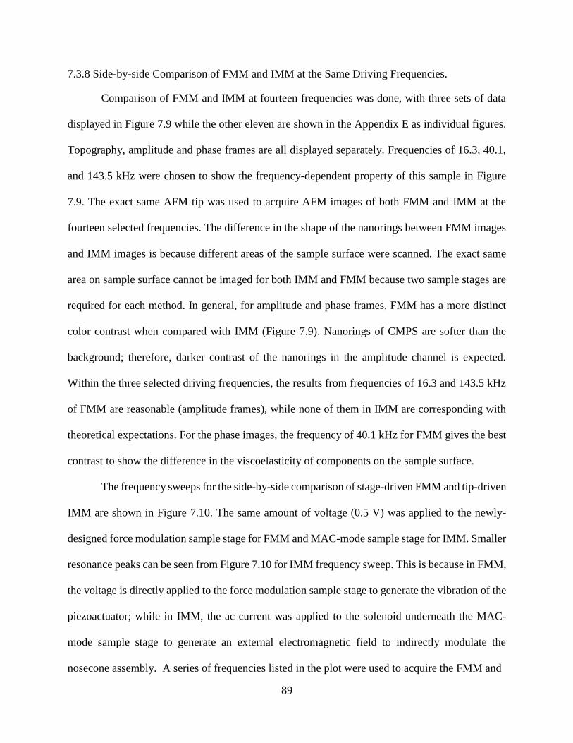
89
7.3.8 Side-by-side Comparison of FMM and IMM at the Same Driving Frequencies.
Comparison of FMM and IMM at fourteen frequencies was done, with three sets of data
displayed in Figure 7.9 while the other eleven are shown in the Appendix E as individual figures.
Topography, amplitude and phase frames are all displayed separately. Frequencies of 16.3, 40.1,
and 143.5 kHz were chosen to show the frequency-dependent property of this sample in Figure
7.9. The exact same AFM tip was used to acquire AFM images of both FMM and IMM at the
fourteen selected frequencies. The difference in the shape of the nanorings between FMM images
and IMM images is because different areas of the sample surface were scanned. The exact same
area on sample surface cannot be imaged for both IMM and FMM because two sample stages are
required for each method. In general, for amplitude and phase frames, FMM has a more distinct
color contrast when compared with IMM (Figure 7.9). Nanorings of CMPS are softer than the
background; therefore, darker contrast of the nanorings in the amplitude channel is expected.
Within the three selected driving frequencies, the results from frequencies of 16.3 and 143.5 kHz
of FMM are reasonable (amplitude frames), while none of them in IMM are corresponding with
theoretical expectations. For the phase images, the frequency of 40.1 kHz for FMM gives the best
contrast to show the difference in the viscoelasticity of components on the sample surface.
The frequency sweeps for the side-by-side comparison of stage-driven FMM and tip-driven
IMM are shown in Figure 7.10. The same amount of voltage (0.5 V) was applied to the newly-
designed force modulation sample stage for FMM and MAC-mode sample stage for IMM. Smaller
resonance peaks can be seen from Figure 7.10 for IMM frequency sweep. This is because in FMM,
the voltage is directly applied to the force modulation sample stage to generate the vibration of the
piezoactuator; while in IMM, the ac current was applied to the solenoid underneath the MAC-
mode sample stage to generate an external electromagnetic field to indirectly modulate the
nosecone assembly. A series of frequencies listed in the plot were used to acquire the FMM and
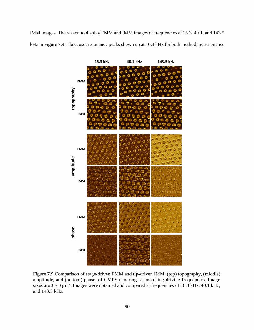
90
IMM images. The reason to display FMM and IMM images of frequencies at 16.3, 40.1, and 143.5
kHz in Figure 7.9 is because: resonance peaks shown up at 16.3 kHz for both method; no resonance
Figure 7.9 Comparison of stage-driven FMM and tip-driven IMM: (top) topography, (middle)
amplitude, and (bottom) phase, of CMPS nanorings at matching driving frequencies. Image
sizes are 3 × 3 μm2. Images were obtained and compared at frequencies of 16.3 kHz, 40.1 kHz,
and 143.5 kHz.
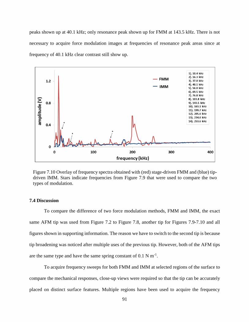
91
peaks shown up at 40.1 kHz; only resonance peak shown up for FMM at 143.5 kHz. There is not
necessary to acquire force modulation images at frequencies of resonance peak areas since at
frequency of 40.1 kHz clear contrast still show up.
7.4 Discussion
To compare the difference of two force modulation methods, FMM and IMM, the exact
same AFM tip was used from Figure 7.2 to Figure 7.8, another tip for Figures 7.9-7.10 and all
figures shown in supporting information. The reason we have to switch to the second tip is because
tip broadening was noticed after multiple uses of the previous tip. However, both of the AFM tips
are the same type and have the same spring constant of 0.1 N m-1.
To acquire frequency sweeps for both FMM and IMM at selected regions of the surface to
compare the mechanical responses, close-up views were required so that the tip can be accurately
placed on distinct surface features. Multiple regions have been used to acquire the frequency
Figure 7.10 Overlay of frequency spectra obtained with (red) stage-driven FMM and (blue) tip-
driven IMM. Stars indicate frequencies from Figure 7.9 that were used to compare the two
types of modulation.

92
sweeps to prove that the differences in the elasticity of the sample cause a frequency shift around
160 kHz for this sample. Based on the previous discussion in this paper, more reliable information
can be obtained from the frequency sweep from stage-driven FMM.
By inputting same amount of voltage to the sample stage, more amplitude response in
FMM than IMM was detected. This is because the current applied to the FMM piezoactuator is
directly vibrating the sample stage, while the current for IMM stage is to generate magnetic field,
then the nosecone is vibrated by the flux of the magnetic field. Higher resolution images were
acquired using FMM than IMM (Figures 7.5). More surface details can be found from this zoom-
in view of FMM than IMM. Based on our experience, it is easier to acquire data using FMM
because IMM is more sensitive to the environment noise and vibration and usually takes longer
time for the AFM to stabilize.
7.5 Conclusion
Nanoring patterns of 4-(chloromethyl)phenyltrichlorosilane (CMPS) were prepared with
particle lithography combined with silane vapor deposition. This test platform is a good candidate
for force modulation studies because of the range of elasticities present in the features of the
surface. The influences of modulation and non-modulation, driving frequency, and vibrational
response have been studied for both force modulation microscopy (FMM) and indirect magnetic
modulation (IMM). The images of FMM and IMM at the exact same driving frequencies have
been compared and discussed. The method of FMM using the newly-designed sample stage proved
to be an easier, more efficient way to obtain high resolution AFM images that can be used to
compare local mechanical differences on a sample.
93
CHAPTER 8. CONCLUSIONS AND FUTURE PROSPECTUS
Nanopores within a film of organosilane were used as miniature containers for depositing
initiators for surface initiated polymerization. Nanostructures of poly(N-allyl glycine) were
generated on Si(111) using particle lithography. Experimental results were characterized step-by-
step with high resolution AFM. The nanostructured surface platform has potential application in
smart coatings, drug delivery, and bioseparations due to the biocompatibility, backbone
degradability and thermal processability of the polymer. For future studies, other polymeric
materials can be patterned on surfaces using the protocols developed in this dissertation.
Thermo-responsive copolypeptoids were pre-synthesized and attached onto patterned
organosilanes using thiol-ene click reaction. The polymer has a narrower distribution of heights
when using the “graft to” approach. Phase transitions of the polymer nanostructures were
investigated using in situ AFM at the molecular level. Experimental results were compared with a
turbidity assay for the aqueous solution of the bulk material. Higher sensitivity was observed with
the in situ AFM study of the shrinkage and entanglement of the polymer chain. The phase transition
of other systems can be studied with this approach for future studies. Further investigations of this
platform in biosensor applications should be promising because of the excellent biocompatibility
of polypeptoids.
Force modulation microscopy (FMM) is commonly used to acquire mechanical properties
of samples concurrent with topographic information. The FMM mode is particularly useful for
studying polymer samples and organic thin films. A sample stage for FMM constructed of
machined polycarbonate was designed and tested. The designed FMM sample stage is compatible
with a tip-mounted AFM configuration. A piezoactuator was mounted within the sample stage to
drive the vibration of the sample in the z-direction. Information of elastic or viscoelastic properties
of samples can be acquired with FMM. Three samples with increasing complexity were selected

94
to test the capabilities of the FMM stage design. High resolution AFM results concurrent with
sample elasticity can be acquired. Future studies will incorporate a liquid cell for the design of the
FMM stage to enable characterizations in liquids. Machined glass components will be used for
constructing a sample stage to enable studies in solvents.
95
REFERENCES
1. Binnig, G.; Quate, C. F.; Gerber, C., Atomic force microscope. Phys. Rev. Lett. 1986, 56,
930-933.
2. Hansma, H. G., Surface biology of DNA by atomic force microscopy. Annu. Rev. Phys.
Chem. 2001, 52, 71-92.
3. Hansma, P. K.; Elings, V. B.; Marti, O.; Bracker, C. E., Scanning tunneling microscopy and
atomic force microscopy - application to biology and technology. Science 1988, 242, 209-216.
4. Hoh, J. H.; Hansma, P. K., Atomic force microscopy for high-resolution imaging in cell
biology. Trends cell biol. 1992, 2, 208-213.
5. Zhong, Q.; Inniss, D.; Kjoller, K.; Elings, V. B., Fractured polymer silica fiber surface studied
by tapping mode atomic-force microscopy. Surf. Sci. 1993, 290, L688-L692.
6. Magonov, S. N.; Reneker, D. H., Characterization of polymer surfaces with atomic force
microscopy. Annu. Rev. Mater. Sci. 1997, 27, 175-222.
7. Bar, G.; Thomann, Y.; Brandsch, R.; Cantow, H. J.; Whangbo, M. H., Factors affecting the
height and phase images in tapping mode atomic force microscopy. Study of phase-separated
polymer blends of poly(ethene-co-styrene) and poly(2,6-dimethyl-1,4-phenylene oxide).
Langmuir 1997, 13, 3807-3812.
8. Mativetsky, J. A.; Palma, M.; Samori, P., Exploring electronic transport in molecular
junctions by conducting atomic force microscopy. In STM and AFM Studies on (bio)molecular
systems: Unravelling the nanoworld, Samori, P., Ed. 2008; Vol. 285, pp 157-202.
9. Mueller, D. J.; Dufrene, Y. F., Atomic force microscopy as a multifunctional molecular
toolbox in nanobiotechnology. Nature Nanotech. 2008, 3, 261-269.
10. Archakov, A. I.; Ivanov, Y. D., Analytical nanobiotechnology for medicine diagnostics.
Mol. Biosyst. 2007, 3, 336-342.
11. Goksu, E. I.; Vanegas, J. M.; Blanchette, C. D.; Lin, W.-C.; Longo, M. L., AFM for
structure and dynamics of biomembranes. BBA-Biomembranes 2009, 1788, 254-266.
12. Fang, F. Z.; Venkatesh, V. C., Diamond cutting of silicon with nanometric finish. CIRP
Annals - Manuf. Technol. 1998, 47, 45-49.
13. Binnig, G.; Gerber, C.; Stoll, E.; Albrecht, T. R.; Quate, C. F., Atomic resolution with
atomic force microscope. Europhys. Lett. 1987, 3, 1281-1286.
14. Maivald, P.; Butt, H. J.; Gould, S. A. C.; Prater, C. B.; Drake, B.; Gurley, J. A.; Elings, V.
B.; Hansma, P. K., Using force modulation to image surface elasticities with the atomic force
microscope Nanotechnology 1991, 2, 103-106.
96
15. Lu, L., Xu, S., Zhang, D., Garno, J. C., Sample stage designed for force modulation
microscopy using a tip-mounted AFM scanner. Anal. Chem. 2015, in submission.
16. Li, J.-R.; Garno, J. C., Indirect modulation of nonmagnetic probes for force modulation
atomic force microscopy. Anal. Chem. 2009, 81, 1699-1706.
17. Caron, A.; Rabe, U.; Reinstadtler, M.; Turner, J. A.; Arnold, W., Imaging using lateral
bending modes of atomic force microscope cantilevers. Appl. Phys. Lett. 2004, 85, 6398-6400.
18. Lehmani, A.; Durand-Vidal, S.; Turq, P., Surface morphology of Nafion 117 membrane by
tapping mode atomic force microscope. J. Appl. Poly. Sci. 1998, 68, 503-508.
19. Prior, M.; Makarovski, A.; Finkelstein, G., Low-temperature conductive tip atomic force
microscope for carbon nanotube probing and manipulation. Appl. Phys. Lett. 2007, 91,053112/1-
053112-3.
20. Saenz, J. J.; Garcia, N.; Grutter, P.; Meyer, E.; Heinzelmann, H.; Wiesendanger, R.;
Rosenthaler, L.; Hidber, H. R.; Gunterodt, H. J., Observation of magnetic forces by the atomic
force microscope. J. Appl. Phys. 1987, 62, 4293-4295.
21. Reviakine, I.; Bergsma-Schutter, W.; Brisson, A., Growth of protein 2-d crystals on
supported planar lipid bilayers imaged in situ by AFM. J. Struct. Biol. 1998, 121, 356-362.
22. Beaulieu, L. Y.; Hatchard, T. D.; Bonakdarpour, A.; Fleischauer, M. D.; Dahn, J. R.,
Reaction of Li with alloy thin films studied by in situ AFM. J. Electrochem. Soc. 2003, 150,
A1457-A1464.
23. Tamada, K.; Hara, M.; Sasabe, H.; Knoll, W., Surface phase behavior of n-alkanethiol self-
assembled monolayers adsorbed on Au(111): An atomic force microscope study. Langmuir
1997, 13, 1558-1566.
24. Wenzler, L. A.; Moyes, G. L.; Raikar, G. N.; Hansen, R. L.; Harris, J. M.; Beebe, T. P.;
Wood, L. L.; Saavedra, S. S., Measurements of single-molecule bond rupture forces between
self-assembled monolayers of organosilanes with the atomic force microscope. Langmuir 1997,
13, 3761-3768.
25. Drake, B.; Prater, C. B.; Weisenhorn, A. L.; Gould, S. A. C.; Albrecht, T. R.; Quate, C. F.;
Cannell, D. S.; Hansma, H. G.; Hansma, P. K., Imaging crystals, polymers and processes in
water with the atomic force microscope. Science 1989, 243, 1586-1589.
26. Domke, J.; Radmacher, M., Measuring the elastic properties of thin polymer films with the
atomic force microscope. Langmuir 1998, 14, 3320-3325.
27. Rong, W. Z.; Pelling, A. E.; Ryan, A.; Gimzewski, J. K.; Friedlander, S. K., Complementary
TEM and AFM force spectroscopy to characterize the nanomechanical properties of nanoparticle
chain aggregates. Nano Lett. 2004, 4, 2287-2292.
97
28. Hoo, C. M.; Starostin, N.; West, P.; Mecartney, M. L., A comparison of atomic force
microscopy (AFM) and dynamic light scattering (DLS) methods to characterize nanoparticle size
distributions. J. Nanopart. Res. 2008, 10, 89-96.
29. Kidoaki, S.; Matsuda, T., Adhesion forces of the blood plasma proteins on self-assembled
monolayer surfaces of alkanethiolates with different functional groups measured by an atomic
force microscope. Langmuir 1999, 15, 7639-7646.
30. Fisher, T. E.; Oberhauser, A. F.; Carrion-Vazquez, M.; Marszalek, P. E.; Fernandez, J. M.,
The study of protein mechanics with the atomic force microscope. Trends Biochem. Sci. 1999,
24, 379-384.
31. Sen, S.; Subramanian, S.; Discher, D. E., Indentation and adhesive probing of a cell
membrane with AFM: Theoretical model and experiments. Biophys. J. 2005, 89, 3203-3213.
32. Li, Q. S.; Lee, G. Y. H.; Ong, C. N.; Lim, C. T., AFM indentation study of breast cancer
cells. Biochem. Biophys. Res. Commun. 2008, 374, 609-613.
33. Thomson, N. H.; Kasas, S.; Smith, B.; Hansma, H. G.; Hansma, P. K., Reversible binding of
DNA to mica for AFM imaging. Langmuir 1996, 12, 5905-5908.
34. Allen, M. J.; Bradbury, E. M.; Balhorn, R., AFM analysis of DNA-protamine complexes
bound to mica. Nucleic Acids Res. 1997, 25, 2221-2226.
35. Singjai, P.; Zhdan, P. A.; Castle, J. E., Observations on the full honeycomb structure of
graphite as imaged by atomic force microscopy. Philos. mag. A 2000, 80, 2445-2456.
36. Arai, T.; Fujihira, M., Effect of tip shape on force distance curves for AFM in aqueous-
electrolytes. J. Electroanal. Chem. 1994, 374, 269-273.
37. Kraemer, G.; Griepentrog, M.; Bonaccurso, E.; Cappella, B., Study of morphology and
mechanical properties of polystyrene-polybutadiene blends with nanometre resolution using
AFM and force-distance curves. Eur. Polym. J. 2014, 55, 123-134.
38. Cappella, B.; Baschieri, P.; Frediani, C.; Miccoli, P.; Ascoli, C., Improvements in AFM
imaging of the spatial variation of force-distance curves: On-line images. Nanotechnology 1997,
8, 82-87.
39. Waltman, R. J.; Guo, X. C., AFM force-distance curves for perfluoropolyether boundary
lubricant films as a function of molecular polarity. Tribol. Lett. 2012, 45, 275-289.
40. Grinevich, O.; Mejiritski, A.; Neckers, D. C., AFM force-distance curve methods for
measuring the kinetics of silicon chemical etching and reactions between silylating agents and a
silicon surface. Langmuir 1999, 15, 2077-2079.
41. Cappella, B.; Kaliappan, S. K.; Sturm, H., Using AFM force-distance curves to study the
glass-to-rubber transition of amorphous polymers and their elastic-plastic properties as a function
of temperature. Macromolecules 2005, 38, 1874-1881.
98
42. Kaliappan, S. K.; Cappella, B., Temperature dependent elastic-plastic behaviour of
polystyrene studied using AFM force-distance curves. Polymer 2005, 46, 11416-11423.
43. Cappella, B.; Stark, W., Adhesion of amorphous polymers as a function of temperature
probed with AFM force-distance curves. J. Colloid Interface Sci. 2006, 296, 507-514.
44. Kim, K.-S.; Lin, Z.; Shrotriya, P.; Sundararajan, S.; Zou, Q., Iterative control approach to
high-speed force-distance curve measurement using AFM: Time-dependent response of PDMS
example. Ultramicroscopy 2008, 108, 911-920.
45. Ebenstein, Y.; Nahum, E.; Banin, U., Tapping mode atomic force microscopy for
nanoparticle sizing: Tip-sample interaction effects. Nano Lett. 2002, 2, 945-950.
46. Bar, G.; Thomann, Y.; Whangbo, M. H., Characterization of the morphologies and
nanostructures of blends of poly(styrene) block-poly(ethene-co-but-1-ene)-block-poly(styrene)
with isotactic and atactic polypropylenes by tapping-mode atomic force microscopy. Langmuir
1998, 14, 1219-1226.
47. Betley, T. A.; Holl, M. M. B.; Orr, B. G.; Swanson, D. R.; Tomalia, D. A.; Baker, J. R.,
Tapping mode atomic force microscopy investigation of poly(amidoamine) dendrimers: Effects
of substrate and pH on dendrimer deformation. Langmuir 2001, 17, 2768-2773.
48. Stocker, W.; Beckmann, J.; Stadler, R.; Rabe, J. P., Surface reconstruction of the lamellar
morphology in a symmetric poly(styrene-block-butadiene-block-methyl methacrylate) triblock
copolymer: A tapping mode scanning force microscope study. Macromolecules 1996, 29, 7502-
7507.
49. Moller, C.; Allen, M.; Elings, V.; Engel, A.; Muller, D. J., Tapping-mode atomic force
microscopy produces faithful high-resolution images of protein surfaces. Biophys. J. 1999, 77,
1150-1158.
50. Fritz, M.; Radmacher, M.; Cleveland, J. P.; Allersma, M. W.; Stewart, R. J.; Gieselmann, R.;
Janmey, P.; Schmidt, C. F.; Hansma, P. K., Imaging globular and filamentous proteins in
physiological buffer solutions with tapping mode atomic-force micrscopy. Langmuir 1995, 11,
3529-3535.
51. Zhong, Q.; Inniss, D.; Kjoller, K.; Elings, V. B., Fractured polymer/silica fiber surface
studied by tapping mode atomic force microscopy. Surf. Sci. 1993, 290, L688-L692.
52. Hansma, P. K.; Cleveland, J. P.; Radmacher, M.; Walters, D. A.; Hillner, P. E.; Bezanilla,
M.; Fritz, M.; Vie, D.; Hansma, H. G.; Prater, C. B.; Massie, J.; Fukunaga, L.; Gurley, J.; Elings,
V., Tapping mode atomic force microscopy in liquids. Appl. Phys. Lett. 1994, 64, 1738-1740.
53. Putman, C. A. J.; Vanderwerf, K. O.; Degrooth, B. G.; Vanhulst, N. F.; Greve, J., Tapping
mode atomic-force microscopy in liquid. Appl. Phys. Lett. 1994, 64, 2454-2456.
99
54. Schmitz, I.; Schreiner, M.; Friedbacher, G.; Grasserbauer, M., Phase imaging as an
extension to tapping mode AFM for the identification of material properties on humidity-
sensitive surfaces. Appl. Surf. Sci. 1997, 115, 190-198.
55. Tamayo, J.; García, R., Deformation, contact time, and phase contrast in tapping mode
scanning force microscopy. Langmuir 1996, 12, 4430-4435.
56. Li, J.-R.; Garno, J. C., Elucidating the role of surface hydrolysis in preparing organosilane
nanostructures via particle lithography. Nano Lett. 2008, 8, 1916-1922.
57. Raghavan, D.; Gu, X.; Nguyen, T.; VanLandingham, M.; Karim, A., Mapping polymer
heterogeneity using atomic force microscopy phase imaging and nanoscale indentation.
Macromolecules 2000, 33, 2573-2583.
58. Kapaklis, V.; Grammatikopoulos, S.; Sordan, R.; Miranda, A.; Traversi, F.; von Kanei, H.;
Trachylis, D.; Poulopoulos, P.; Politis, C., Nanolithographic templates using diblock copolymer
films on chemically heterogeneous substrates. J. Nanosci. Nanotechnol. 2010, 10, 6056-6061.
59. Schon, P.; Bagdi, K.; Molnar, K.; Markus, P.; Pukanszky, B.; Vancso, G. J., Quantitative
mapping of elastic moduli at the nanoscale in phase separated polyurethanes by AFM. Eur.
Polym. J. 2011, 47, 692-698.
60. Wilbur, J. L.; Biebuyck, H. A.; Macdonald, J. C.; Whitesides, G. M., Scanning force
microscopies can image patterned self-assembled monolayers. Langmuir 1995, 11, 825-831.
61. Nysten, B.; Legras, R.; Costa, J. L., Atomic-force microscopy imaging of viscoelastic
properties in toughened polyppopylene resins. J. Appl. Phys. 1995, 78, 5953-5958.
62. Nie, H. Y.; Motomatsu, M.; Mizutani, W.; Tokumoto, H., Local modification of elastic
properties of polystyrene-polyethyleneoxide blend surfaces. J. Vac. Sci. Technol. B 1995, 13,
1163-1166.
63. Galuska, A. A.; Poulter, R. R.; McElrath, K. O., Force modulation AFM of elastomer
blends: Morphology, fillers and cross-linking. Surf. Interface Anal. 1997, 25, 418-429.
64. Gilmore, I. S.; Seah, M. P.; Johnstone, J. E., Quantification issues in ToF-SSIMS and AFM
co-analysis in two-phase systems, exampled by a polymer blend. Surf. Interface Anal. 2003, 35,
888-896.
65. Krol, S.; Ross, M.; Sieber, M.; Kunneke, S.; Galla, H. J.; Janshoff, A., Formation of three-
dimensional protein-lipid aggregates in monolayer films induced by surfactant protein B.
Biophys. J. 2000, 79, 904-918.
66. Clair, B.; Arinero, R.; Leveque, G.; Ramonda, M.; Thibaut, B., Imaging the mechanical
properties of wood cell wall layers by atomic force modulation microscopy. Iawa J. 2003, 24,
223-230.
100
67. Haga, H.; Nagayama, M.; Kawabata, K., Imaging mechanical properties of living cells by
scanning probe microscopy. Curr. Nanosci. 2007, 3, 97-103.
68. Sasaki, S.; Morimoto, M.; Haga, H.; Kawabata, K.; Ito, E.; Ushiki, T.; Abe, K.; Sambongi,
T., Elastic properties of living fibroblasts as imaged using force modulation mode in atomic
force microscopy. Arch. of Histol. Cytol. 1998, 61, 57-63.
69. Fritz, M.; Radmacher, M.; Petersen, N.; Gaub, H. E., Visuallization and identification of
intracellular structures by force modulation microscopy and drug-induced degradation. J. Vac.
Sci. Technol. B 1994, 12, 1526-1529.
70. Sbrana, F.; Ghulinyan, M.; Pavesi, L., Force modulation microscopy of multilayered porous
silicon samples. Phys. Status Solidi A 2005, 202, 1492-1496.
71. Sahoo, N.; Thakur, S.; Senthilkumar, M.; Das, N. C., Surface viscoelasticity studies of
Gd2O3, SiO2 optical thin films and multilayers using force modulation and force-distance
scanning probe microscopy. Appl. Surf. Sci. 2003, 206, 271-293.
72. Resch, R.; Friedbacher, G.; Grasserbauer, M.; Kanniainen, T.; Lindroos, S.; Leskela, M.;
Niinisto, L., Lateral force microscopy and force modulation microscopy on SILAR-grown lead
sulfide samples. Appl. Surf. Sci. 1997, 120, 51-57.
73. Wozniak, M. J.; Ryszkowska, J.; Szymborski, T.; Chen, G.; Tateishi, T.; Kurzydlowski, K.
J., Application of phase imaging and force modulation mode for description of dispersion of
carbon nanotubes in polyol matrix. Mater. Sci-Poland 2008, 26, 245-253.
74. Schonherr, H.; Tocha, E.; Vancso, G. J., Friction and surface dynamics of polymers on the
nanoscale by AFM. In STM and AFM Studies on (bio)molecular system: unravelling the
nanoworld, Samori, P., Ed. 2008; Vol. 285, pp 103-156.
75. DeVecchio, D.; Bhushan, B., Localized surface elasticity measurements using an atomic
force microscope. Rev. Sci. Instrum. 1997, 68, 4498-4505.
76. Troyon, M.; Wang, Z.; Pastre, D.; Lei, H. N.; Hazotte, A., Force modulation microscopy for
the study of stiff materials. Nanotechnology 1997, 8, 163-171.
77. Radmacher, M.; Tilmann, R. W.; Gaub, H. E., Imaging viscoelasticity by force modulation
with the atomic force microscope. Biophys. J. 1993, 64, 735-742.
78. Overney, R. M.; Takano, H.; Fujihira, M., Elastic compliances measured by atomic-force
microscopy. Europhys. Lett. 1994, 26, 443-447.
79. Akari, S. O.; Vandervegte, E. W.; Grim, P. C. M.; Belder, G. F.; Koutsos, V.; Tenbrinke, G.;
Hadziioannou, G., Imaging of signle polymer-chains based on their elasticity. Appl. Phys. Lett.
1994, 65, 1915-1917.
101
80. Kajiyama, T.; Tanaka, K.; Ohki, I.; Ge, S. R.; Yoon, J. S.; Takahara, A., Imaging of dynamic
viscoelastic properties of a phase-separated polymer surface by forced oscillation atomic-force
microscopy. Macromolecules 1994, 27, 7932-7934.
81. Wang, M.; Miyake, S.; Matsunuma, S., Nanowear studies of PFPE lubricant on magnetic
perpendicular recording DLC-film-coated disk by lateral oscillation test. Wear 2005, 259, 1332-
1342.
82. Yang, C.; Chen, Y.; Wang, T.; Huang, W., A comparative experimental study on sample
excitation and probe excitation in force modulation atomic force microscopy. Meas. Sci.
Technol. 2013, 24, 025403/1-025403/6.
83. Li, F. B.; Thompson, G. E.; Newman, R. C., Force modulation atomic force microscopy:
background, development and application to electrodeposited cerium oxide films. Appl. Surf. Sci.
1998, 126, 21-33.
84. Beake, B. D.; Leggett, G. J.; Shipway, P. H., Frictional, adhesive and mechanical properties
of polyester films probed by scanning force microscopy. Surf. Interface Anal. 1999, 27, 1084-
1091.
85. Yamamoto, S.; Yamada, H., Interpretation of direct and indirect force modulation methods
using polymer films. Langmuir 1997, 13, 4861-4864.
86. Lin, C.-C.; Chang, K.-H.; Lin, K.-C.; Su, W.-F., In situ probe nanophase transition in
nanocomposite using thermal AFM. Compos. Sci. Technol. 2009, 69, 1180-1186.
87. Pietrement, O.; Troyon, M., Quantitative study of shear modulus and interfacial shear
strength by combining modulated lateral force and magnetic force modulation microscopies.
Surf. Interface Anal. 2001, 31, 1060-1067.
88. Xu, X.; Koslowski, M.; Raman, A., Dynamics of surface-coupled microcantilevers in force
modulation atomic force microscopy - magnetic vs. dither piezo excitation. J. Appl. Phys. 2012,
111, 054303/1-054303/5.
89. Jourdan, J. S.; Cruchon-Dupeyrat, S. J.; Huan, Y.; Kuo, P. K.; Liu, G. Y., Imaging
nanoscopic elasticity of thin film materials by atomic force microscopy: Effects of force
modulation frequency and amplitude. Langmuir 1999, 15, 6495-6504.
90. Popa, A. M.; Angeloni, S.; Buergi, T.; Hubbell, J. A.; Heinzelmann, H.; Pugin, R., Dynamic
perspective on the function of thermoresponsive nanopores from in situ AFM and ATIZ-IR
investigations. Langmuir 2010, 26, 15356-15365.
91. Schonherr, H.; Frank, C. W., Ultrathin films of poly(ethylene oxides) on oxidized silicon. 2.
In situ study of crystallization and melting by hot stage AFM. Macromolecules 2003, 36, 1199-
1208.
92. Hobbs, J. K., In-situ AFM of polymer crystallization. Chin. J. Polym. Sci. 2003, 21, 135-
140.
102
93. Hu, Z. J.; Du, B. Y.; Zhang, F. J.; Xie, F. C.; He, T. B., In situ study of nanostructure and
morphological development during the crystal-mesophase transition of poly(di-n-hexylsilane)
and poly(di-n-butylsilane) by X-ray and hot-stage AFM. Polymer 2002, 43, 6005-6012.
94. Wiedemair, J.; Serpe, M. J.; Kim, J.; Masson, J.-F.; Lyon, L. A.; Mizaikoff, B.; Kranz, C.,
In-situ AFM studies of the phase-transition behavior of single thermoresponsive hydrogel
particles. Langmuir 2007, 23, 130-137.
95. Mart, R. J.; Osborne, R. D.; Stevens, M. M.; Ulijn, R. V., Peptide-based stimuli-responsive
biomaterials. Soft Matter 2006, 2, 822-835.
96. Wang, J.; Gibson, M. I.; Barbey, R.; Xiao, S.-J.; Klok, H.-A., Nonfouling polypeptide
brushes via surface-initiated polymerization of Nε-oligo(ethylene glycol)succinate-L-lysine N-
carboxyanhydride. Macromol. Rapid Commun. 2009, 30, 845-850.
97. Statz, A. R.; Barron, A. E.; Messersmith, P. B., Protein, cell and bacterial fouling resistance
of polypeptoid-modified surfaces: effect of side-chain chemistry. Soft Matter 2008, 4, 131-139.
98. Lunn, J. D.; Shantz, D. F., Peptide brush-ordered mesoporous silica nanocomposite
materials. Chem. Mater. 2009, 21, 3638-3648.
99. Zhang, D.; Lahasky, S. H.; Guo, L.; Lee, C.-U.; Lavan, M., Polypeptoid materials: Current
status and future perspectives. Macromolecules 2012, 45, 5833-5841.
100. Guo, L.; Zhang, D., Cyclic poly(α-peptoid)s and their block copolymers from N-
heterocyclic carbene-mediated ring-opening polymerizations of N-substituted N-
carboxylanhydrides. J. Am. Chem. Soc. 2009, 131, 18072-18074.
101. Schneider, M.; Fetsch, C.; Amin, I.; Jordan, R.; Luxenhofer, R., Polypeptoid brushes by
surface-initiated polymerization of N-substituted glycine N-carboxyanhydrides. Langmuir 2013,
29, 6983-6988.
102. Britland, S.; Perezarnaud, E.; Clark, P.; McGinn, B.; Connolly, P.; Moores, G.,
Micropatterning proteins and synthetic peptides on solid supports - a novel application for
microelectronics fabrication technology. Biotechnol. Progress 1992, 8, 155-160.
103. Hadjichristidis, N.; Iatrou, H.; Pitsikalis, M.; Sakellariou, G., Synthesis of well-defined
polypeptide-based materials via the ring-opening polymerization of alpha-amino acid N-
carboxyanhydrides. Chem. Rev. 2009, 109, 5528-5578.
104. Kratzmuller, T.; Appelhans, D.; Braun, H. G., Ultrathin microstructured polypeptide layers
by surface-initiated polymerization on microprinted surfaces. Adv. Mater. 1999, 11, 555-558.
105. Wang, Y. L.; Chang, Y. C., Patterning of polypeptide thin films by the combination of
surface-initiated vapor-deposition polymerization and photolithography. Adv. Mater. 2003, 15,
290-293.
103
106. Edmondson, S.; Osborne, V. L.; Huck, W. T. S., Polymer brushes via surface-initiated
polymerizations. Chem. Soc. Rev. 2004, 33, 14-22.
107. Sparks, B. J.; Ray, J. G.; Savin, D. A.; Stafford, C. M.; Patton, D. L., Synthesis of thiol-
clickable and block copolypeptide brushes via nickel-mediated surface initiated polymerization
of [small alpha]-amino acid N-carboxyanhydrides (NCAs). Chem. Commun. 2011, 47, 6245-
6247.
108. Whitesell, J. K.; Chang, H. K., Directionally aligned helical peptides on surfaces. Science
1993, 261, 73-76.
109. Chang, Y. C.; Frank, C. W., Grafting of poly(gamma-benzyl-L-glutamate) on chemically
modified silicon oxide surfaces. Langmuir 1996, 12, 5824-5829.
110. Chang, Y.-C.; Frank, C. W., Vapor deposition−polymerization of α-amino acid n-carboxy
anhydride on the silicon(100) native oxide surface. Langmuir 1998, 14, 326-334.
111. Heise, A.; Menzel, H.; Yim, H.; Foster, M. D.; Wieringa, R. H.; Schouten, A. J.; Erb, V.;
Stamm, M., Grafting of polypeptides on solid substrates by initiation of N-carboxyanhydride
polymerization by amino-terminated self-assembled monolayers. Langmuir 1997, 13, 723-728.
112. Higuchi, M.; Ushiba, K.; Kawaguchi, M., Structural control of peptide-coated gold
nanoparticle assemblies by the conformational transition of surface peptides. J. Colloid Interface
Sci. 2007, 308, 356-363.
113. Higuchi, M.; Koga, T.; Taguchi, K.; Kinoshita, T., Fabrication of vertically and
unidirectionally oriented polypeptide assemblies on self-assembled monolayers by stepwise
polymerization. Chem. Commun. 2002, 1126-1127.
114. Luijten, J.; Vorenkamp, E. J.; Schouten, A. J., Reversible helix sense inversion in surface-
grafted poly(beta-phenethyl-L-aspartate) films. Langmuir 2007, 23, 10772-10778.
115. Wang, Y. L.; Chang, Y. C., Grafting of homo- and block co-polypeptides on solid
substrates by an improved surface-initiated vapor deposition polymerization. Langmuir 2002, 18,
9859-9866.
116. Zheng, W.; Frank, C. W., Surface-initiated vapor deposition polymerization of poly(γ-
benzyl-l-glutamate): Optimization and mechanistic studies. Langmuir 2009, 26, 3929-3941.
117. Wieringa, R. H.; Siesling, E. A.; Geurts, P. F. M.; Werkman, P. J.; Vorenkamp, E. J.; Erb,
V.; Stamm, M.; Schouten, A. J., Surface grafting of poly (L-glutamates). 1. Synthesis and
characterization. Langmuir 2001, 17, 6477-6484.
118. Wieringa, R. H.; Siesling, E. A.; Werkman, P. J.; Angerman, H. J.; Vorenkamp, E. J.;
Schouten, A. J., Surface grafting of poly(L-glutamates). 2. Helix orientation. Langmuir 2001, 17,
6485-6490.
104
119. Wieringa, R. H.; Siesling, E. A.; Werkman, P. J.; Vorenkamp, E. J.; Schouten, A. J.,
Surface grafting of poly(L-glutamates). 3. Block copolymerization. Langmuir 2001, 17, 6491-
6495.
120. Wu, J.-C.; Wang, Y.; Chen, C.-C.; Chang, Y.-C., Biomimetic synthesis of silica films
directed by polypeptide brushes. Chem. Mater. 2008, 20, 6148-6156.
121. Wang, Y. L.; Chang, Y. C., Synthesis and conformational transition of surface-tethered
polypeptide: Poly(L-lysine). Macromolecules 2003, 36, 6511-6518.
122. Wang, Y. L.; Chang, Y. C., Synthesis and conformational transition of surface-tethered
polypeptide: Poly(L-glutamic acid). Macromolecules 2003, 36, 6503-6510.
123. Deming, T. J., Transition metal-amine initiators for preparation of well-defined
poly(gamma-benzyl L-glutamate). J. Am. Chem. Soc. 1997, 119, 2759-2760.
124. Deming, T. J.; Curtin, S. A., Chain initiation efficiency in cobalt- and nickel-mediated
polypeptide synthesis. J. Am. Chem. Soc. 2000, 122, 5710-5717.
125. Brzezinska, K. R.; Deming, T. J., Synthesis of ABA triblock copolymers via acyclic diene
metathesis polymerization and living polymerization of alpha-amino acid-N-carboxyanhydrides.
Macromolecules 2001, 34, 4348-4354.
126. Witte, P.; Menzel, H., Nickel-mediated surface grafting from polymerization of α-Amino
acid-N-carboxyanhydrides. Macromol. Chem. Phys. 2004, 205, 1735-1743.
127. Zhang, J.; Li, Y.; Zhang, X.; Yang, B., Colloidal self-assembly meets nanofabrication:
From two-dimensional colloidal crystals to nanostructure arrays. Adv. Mater. 2010, 22, 4249-
4269.
128. Chen, T.; Amin, I.; Jordan, R., Patterned polymer brushes. Chem. Soc. Rev. 2012, 41, 3280-
3296.
129. Penner, R. M., Rapid, wafer-scale laser nanoprinting of polymer surfaces. ACS Nano 2011,
5, 690-692.
130. Valsesia, A.; Lisboa, P.; Colpo, P.; Rossi, F., Fabrication of polypyrrole-based
nanoelectrode arrays by colloidal lithography. Anal. Chem. 2006, 78, 7588-7591.
131. Agheli, H.; Sutherland, D. S., Nanofabrication of polymer surfaces utilizing colloidal
lithography and ion etching. Ieee Trans. Nanobiosci. 2006, 5, 9-14.
132. Lu, Y.; Chen, S. C., Micro and nano-fabrication of biodegradable polymers for drug
delivery. Adv. Drug Delivery Rev. 2004, 56, 1621-1633.
133. Schepelina, O.; Zharov, I., PNIPAAM-modified nanoporous colloidal films with positive
and negative temperature gating. Langmuir 2007, 23, 12704-12709.
105
134. Acikgoz, C.; Ling, X. Y.; Phang, I. Y.; Hempenius, M. A.; Reinhoudt, D. N.; Huskens, J.;
Vancso, G. J., Fabrication of freestanding nanoporous polyethersulfone membranes using
organometallic polymer resists patterned by nanosphere lithography. Adv. Mater. 2009, 21,
2064-2067.
135. Ling, X. Y.; Acikgoz, C.; Phang, I. Y.; Hempenius, M. A.; Reinhoudt, D. N.; Vancso, G. J.;
Huskens, J., 3D ordered nanostructures fabricated by nanosphere lithography using an
organometallic etch mask Nanoscale 2010, 2, 1455-1460.
136. Santos, L.; Martin, P.; Ghilane, J.; Lacaze, P.-C.; Randriamahazaka, H.; Abrantes, L. M.;
Lacroix, J.-C., Electrosynthesis of well-organized nanoporous poly(3,4-ethylenedioxythiophene)
by nanosphere lithography. Electrochem. Commun. 2010, 12, 872-875.
137. Hsiao, Y. S.; Chien, F. C.; Huang, J. H.; Chen, C. P.; Kuo, C. W.; Chu, C. W.; Chen, P. L.,
Facile transfer method for fabricating light-harvesting systems for polymer solar cells. J. Phys.
Chem. C 2011, 115, 11864-11870.
138. Beryozkina, T.; Boyko, K.; Khanduyeva, N.; Senkovskyy, V.; Horecha, M.; Oertel, U.;
Simon, F.; Stamm, M.; Kiriy, A., Grafting of polyfluorene by surface-initiated suzuki
polycondensation. Angew. Chem., Int. Ed. 2009, 48, 2695-2698.
139. Chen, T.; Chang, D. P.; Jordan, R.; Zauscher, S., Colloidal lithography for fabricating
patterned polymer-brush microstructures. Beilstein J. Nanotechnol. 2012, 3, 397-403.
140. Chen, T.; Jordan, R.; Zauscher, S., Polymer brush patterning using self-assembled
microsphere monolayers as microcontact printing stamps. Soft Matter 2011, 7, 5532-5535.
141. Bognar, J.; Szucs, J.; Dorko, Z.; Horvath, V.; Gyurcsanyi, R. E., Nanosphere lithography as
a versatile method to generate surface-imprinted polymer films for selective protein recognition.
Adv. Funct. Mater. 2013, 23, 4703-4709.
142. Pernites, R. B.; Foster, E. L.; Felipe, M. J. L.; Robinson, M.; Advincula, R. C., Patterned
surfaces combining polymer brushes and conducting polymer via colloidal template
electropolymerization. Adv. Mater. 2011, 23, 1287-1292.
143. Saner, C. K.; Lusker, K. L.; LeJeune, Z. M.; Serem, W. K.; Garno, J. C., Self-assembly of
octadecyltrichlorosilane: Surface structures formed using different protocols of particle
lithography. Beilstein J. Nanotechnol. 2012, 3, 114-122.
144. Li, J.-R.; Garno, J. C., Elucidating the role of surface hydrolysis in preparing organosilane
nanostructures via particle lithography. Nano Letters 2008, 8, 1916-1922.
145. Robinson, J. W.; Schlaad, H., A versatile polypeptoid platform based on N-allyl glycine.
Chem. Commun. 2012, 48, 7835-7837.
146. Jones, D. M.; Smith, J. R.; Huck, W. T. S.; Alexander, C., Variable adhesion of
micropatterned thermoresponsive polymer brushes: AFM investigations of poly (N-
106
isopropylacrylamide) brushes prepared by surface-initiated polymerizations. Adv. Mater. 2002,
14, 1130-1134.
147. Kelley, T. W.; Schorr, P. A.; Johnson, K. D.; Tirrell, M.; Frisbie, C. D., Direct force
measurements at polymer brush surfaces by atomic force microscopy. Macromolecules 1998, 31,
4297-4300.
148. Kitano, K.; Inoue, Y.; Matsuno, R.; Takai, M.; Ishihara, K., Nanoscale evaluation of
lubricity on well-defined polymer brush surfaces using QCM-D and AFM. Colloids Surf. B
2009, 74, 350-357.
149. Lemieux, M.; Usov, D.; Minko, S.; Stamm, M.; Shulha, H.; Tsukruk, V. V., Reorganization
of binary polymer brushes: Reversible switching of surface microstructures and nanomechanical
properties. Macromolecules 2003, 36, 7244-7255.
150. Yamamoto, S.; Ejaz, M.; Tsujii, Y.; Matsumoto, M.; Fukuda, T., Surface interaction forces
of well-defined, high-density polymer brushes studied by atomic force microscopy. 1. Effect of
chain length. Macromolecules 2000, 33, 5602-5607.
151. Advincula, R.; Zhou, Q. G.; Park, M.; Wang, S. G.; Mays, J.; Sakellariou, G.; Pispas, S.;
Hadjichristidis, N., Polymer brushes by living anionic surface initiated polymerization on flat
silicon (SiO(x)) and gold surfaces: Homopolymers and block copolymers. Langmuir 2002, 18,
8672-8684.
152. Kolb, H. C.; Finn, M. G.; Sharpless, K. B., Click chemistry: Diverse chemical function
from a few good reactions. Angew Chem., Int. Ed. 2001, 40, 2004-2021.
153. Hensarling, R. M.; Doughty, V. A.; Chan, J. W.; Patton, D. L., "Clicking" polymer brushes
with thiol-yne chemistry: Indoors and out. J. Am. Chem. Soc. 2009, 131, 14673-14675.
154. Engler, A. C.; Lee, H.-i.; Hammond, P. T., Highly efficient "grafting onto" a polypeptide
backbone using click chemistry. Angew Chem., Int. Ed. 2009, 48, 9334-9338.
155. Nečas, D.; Klapetek, P., Gwyddion: an open-source software for SPM data analysis.
Central European Journal of Physics 2012, 10, 181-188.
156. Belgardt, C.; Sowade, E.; Blaudeck, T.; Baumgartel, T.; Graaf, H.; von Borczyskowski, C.;
Baumann, R. R., Inkjet printing as a tool for the patterned deposition of octadecylsiloxane
monolayers on silicon oxide surfaces. Physical Chemistry Chemical Physics 2013, 15, 7494-
7504.
157. Fadeev, A. Y.; McCarthy, T. J., Self-assembly is not the only reaction possible between
alkyltrichlorosilanes and surfaces: Monomolecular and oligomeric covalently attached layers of
dichloro- and trichloroalkylsilanes on silicon. Langmuir 2000, 16, 7268-7274.
158. Ulman, A., Self-assembled monolayers of alkyltrichiorosilanes: Building blocks for future
organic materials. Adv. Mater. 1990, 2, 573-582.

107
159. Chen, T.; Ferris, R.; Zhang, J.; Ducker, R.; Zauscher, S., Stimulus-responsive polymer
brushes on surfaces: Transduction mechanisms and applications. Prog. Polym. Sci. 2010, 35, 94-
112.
160. Ma, D.; Chen, H.; Shi, D.; Li, Z.; Wang, J., Preparation and characterization of thermo-
responsive PDMS surfaces grafted with poly(N-isopropylacrylamide) by benzophenone-initiated
photopolymerization. J. Colloid Interface Sci. 2009, 332, 85-90.
161. Guo, H.; Ulbricht, M., Preparation of thermo-responsive polypropylene membranes via
surface entrapment of poly(N-isopropylacrylamide)-containing macromolecules. J. Membr. Sci.
2011, 372, 331-339.
162. Nagase, K.; Akimoto, A. M.; Kobayashi, J.; Kikuchi, A.; Akiyama, Y.; Kanazawa, H.;
Okano, T., Effect of reaction solvent on the preparation of thermo-responsive stationary phase
through a surface initiated atom transfer radical polymerization. J. Chromatogr. A 2011, 1218,
8617-8628.
163. Ayano, E.; Okada, Y.; Sakamoto, C.; Kanazawa, H.; Kikuchi, A.; Okano, T., Study of
temperature-responsibility on the surfaces of a thermo-responsive polymer modified stationary
phase. J. Chromatogr. A 2006, 1119, 51-57.
164. Hirose, M.; Yamato, M.; Kwon, O. H.; Harimoto, M.; Kushida, A.; Shimizu, T.; Kikuchi,
A.; Okano, T., Temperature-responsive surface for novel co-culture systems of hepatocytes with
endothelial cells: 2-D patterned and double layered co-cultures. Yonsei Med. J. 2000, 41, 803-
813.
165. Bullett, N. A.; Talib, R. A.; Short, R. D.; McArthur, S. L.; Shard, A. G., Chemical and
thermo-responsive characterisation of surfaces formed by plasma polymerisation of N-isopropyl
acrylamide. Surf. Interface Anal. 2006, 38, 1109-1116.
166. Hu, Z. B.; Chen, Y. Y.; Wang, C. J.; Zheng, Y. D.; Li, Y., Polymer gels with engineered
environmentally responsive surface patterns. Nature 1998, 393, 149-152.
167. Yamato, M.; Konno, C.; Utsumi, M.; Kikuchi, A.; Okano, T., Thermally responsive
polymer-grafted surfaces facilitate patterned cell seeding and co-culture. Biomaterials 2002, 23,
561-567.
168. Pan, K.; Zhang, X.; Cao, B., Surface-initiated atom transfer radical polymerization of
regenerated cellulose membranes with thermo-responsive properties. Polym. Int. 2010, 59, 733-
737.
169. Park, J. K.; Kim, K. S.; Yeom, J.; Jung, H. S.; Hahn, S. K., Facile surface modification and
application of temperature responsive poly(N-isopropylacrylamide-co-dopamine
methacrylamide). Macromol. Chem. Phys. 2012, 213, 2130-2135.
170. Li, J.; He, W.-D.; Sun, X.-L., Preparation of poly(styrene-b-N-isopropylacrylamide)
micelles surface-linked with gold nanoparticles and thermo-responsive ultraviolet-visible
absorbance. J. Polym. Sci., Part A: Polym. Chem. 2007, 45, 5156-5163.
108
171. Park, H. H.; Lee, T. R., Thermo- and pH-responsive hydrogel-coated gold nanoparticles
prepared from rationally designed surface-confined initiators. J. Nanopart. Res. 2011, 13, 2909-
2918.
172. Wu, D.; Liu, X.; Yu, S.; Liu, M.; Gao, C., Modification of aromatic polyamide thin-film
composite reverse osmosis membranes by surface coating of thermo-responsive copolymers
P(NIPAM-co-Am). I: Preparation and characterization. J. Membr. Sci. 2010, 352, 76-85.
173. Mizutani, A.; Nagase, K.; Kikuchi, A.; Kanazawa, H.; Akiyama, Y.; Kobayashi, J.;
Annaka, M.; Okano, T., Preparation of thermo-responsive polymer brushes on hydrophilic
polymeric beads by surface-initiated atom transfer radical polymerization for a highly resolutive
separation of peptides. J. Chromatogr. A 2010, 1217, 5978-5985.
174. de Las Heras Alarcon, C.; Twaites, B.; Cunliffe, D.; Smith, J. R.; Alexander, C., Grafted
thermo- and pH responsive co-polymers: surface-properties and bacterial adsorption. Int. J.
Pharm. 2005, 295, 77-91.
175. Laloyaux, X.; Mathy, B.; Nysten, B.; Jonas, A. M., Surface and bulk collapse transitions of
thermo responsive polymer brushes. Langmuir 2010, 26, 838-847.
176. Park, S.; Zhong, M.; Lee, T.; Paik, H.-J.; Matyjaszewski, K., Modification of the surfaces
of silicon wafers with temperature-responsive cross-linkable poly oligo(ethylene oxide)
methacrylate -based star polymers. ACS Appl. Mater. Interfaces 2012, 4, 5949-5955.
177. Medel, S.; Manuel Garcia, J.; Garrido, L.; Quijada-Garrido, I.; Paris, R., Thermo- and pH-
responsive gradient and block copolymers based on 2-(2-methoxyethoxy)ethyl methacrylate
synthesized via atom transfer radical polymerization and the formation of thermoresponsive
surfaces. J. Polym. Sci., Part A: Polym. Chem. 2011, 49, 690-700.
178. Wischerhoff, E.; Zacher, T.; Laschewsky, A.; Rekai, E., Direct observation of the lower
critical solution temperature of surface-attached thermo-responsive hydrogels by surface
plasmon resonance. Angew. Chem., Int. Ed. 2000, 39, 4602-4604.
179. Sousa, M. E.; Broer, D. J.; Bastiaansen, C. W. M.; Freund, L. B.; Crawford, G. P., Isotropic
"islands" in a cholesteric "sea": Patterned thermal expansion for responsive surface topologies".
Adv. Mater. 2006, 18, 1842-1845.
180. Bulychev, N.; Confortini, O.; Kopold, P.; Dirnberger, K.; Schauer, T.; Du Prez, F. E.;
Zubov, V.; Eisenbach, C. D., Application of thermo-responsive poly(methyl vinyl ether)
containing copolymers in combination with ultrasonic treatment for pigment surface
modification in pigment dispersions. Polymer 2007, 48, 2636-2643.
181. Dey, S.; Kellam, B.; Alexander, M. R.; Alexander, C.; Rose, F. R. A. J., Enzyme-passage
free culture of mouse embryonic stem cells on thermo-responsive polymer surfaces. J. Mater.
Chem. 2011, 21, 6883-6890.
182. Edmondson, S.; Osborne, V. L.; Huck, W. T. S., Polymer brushes via surface-initiated
polymerizations. Chemical Society Reviews 2004, 33, 14-22.
109
183. Prakash, S.; Long, T. M.; Selby, J. C.; Moore, J. S.; Shannon, M. A., "Click" modification
of silica surfaces and glass microfluidic channels. Anal. Chem. 2007, 79, 1661-1667.
184. Wu, X.-M.; Wang, L.-L.; Wang, Y.; Gu, J.-S.; Yu, H.-Y., Surface modification of
polypropylene macroporous membrane by marrying RAFT polymerization with click chemistry.
J. Membr. Sci. 2012, 421, 60-68.
185. Yameen, B.; Ali, M.; Alvarez, M.; Neumann, R.; Ensinger, W.; Knoll, W.; Azzaroni, O., A
facile route for the preparation of azide-terminated polymers. "Clicking" polyelectrolyte brushes
on planar surfaces and nanochannels. Polym. Chem. 2010, 1, 183-192.
186. Chen, G.; Tao, L.; Mantovani, G.; Ladmiral, V.; Burt, D. P.; Macpherson, J. V.; Haddleton,
D. M., Synthesis of azide/alkyne-terminal polymers and application for surface functionalisation
through a [2 + 3] Huisgen cycloaddition process, "click chemistry". Soft Matter 2007, 3, 732-
739.
187. Proks, V.; Jaros, J.; Pop-Georgievski, O.; Kucka, J.; Popelka, S.; Dvorak, P.; Hampl, A.;
Rypacek, F., "Click & seed" approach to the biomimetic modification of material surfaces.
Macromol. Biosci. 2012, 12, 1232-1242.
188. Haensch, C.; Erdmenger, T.; Fijten, M. W. M.; Hoeppener, S.; Schubert, U. S., Fast surface
modification by microwave assisted click reactions on silicon substrates. Langmuir 2009, 25,
8019-8024.
189. Ru, X.; Zeng, X.; Li, Z.; Evans, D. J.; Zhan, C.; Tang, Y.; Wang, L.; Liu, X., Bioinspired
polymer functionalized with a diiron carbonyl model complex and its assembly onto the surface
of a gold electrode via "click" chemistry. J. Polym. Sci., Part A: Polym. Chem. 2010, 48, 2410-
2417.
190. Drockenmuller, E.; Colinet, I.; Damiron, D.; Gal, F.; Perez, H.; Carrot, G., Efficient
approaches for the surface modification of platinum nanoparticles via click chemistry.
Macromolecules 2010, 43, 9371-9375.
191. El Habnouni, S.; Darcos, V.; Garric, X.; Lavigne, J.-P.; Nottelet, B.; Coudane, J., Mild
methodology for the versatile chemical modification of polylactide surfaces: Original
combination of anionic and click chemistry for biomedical applications. Adv. Funct. Mater.
2011, 21, 3321-3330.
192. Chen, J.; Xiang, J.; Cai, Z.; Yong, H.; Wang, H.; Zhang, L.; Luo, W.; Min, H., Synthesis of
hydrophobic polymer brushes on silica nanoparticles via the combination of surface-initiated
ATRP, ROP and click chemistry. J. Macromol. Sci. A, Pure Appl. Chem. 2010, 47, 655-662.
193. Bayraktar, A.; Saracoglu, B.; Golgelioglu, C.; Tuncel, A., Click-chemistry for surface
modification of monodisperse-macroporous particles. J. Colloid Interface Sci. 2012, 365, 63-71.
194. Chen, J. C.; Wang, Y. P.; Wang, H. D.; Wei, S. Y.; Li, H. J.; Yan, X. D., Preparation of
polymer brushes on attapulgite surfaces via a combination of CROP and click reaction. Chin.
Chem. Lett. 2010, 21, 496-500.
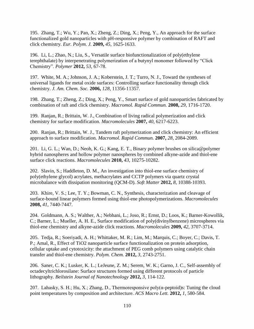
110
195. Zhang, T.; Wu, Y.; Pan, X.; Zheng, Z.; Ding, X.; Peng, Y., An approach for the surface
functionalized gold nanoparticles with pH-responsive polymer by combination of RAFT and
click chemistry. Eur. Polym. J. 2009, 45, 1625-1633.
196. Li, L.; Zhao, N.; Liu, S., Versatile surface biofunctionalization of poly(ethylene
terephthalate) by interpenetrating polymerization of a butynyl monomer followed by “Click
Chemistry”. Polymer 2012, 53, 67-78.
197. White, M. A.; Johnson, J. A.; Koberstein, J. T.; Turro, N. J., Toward the syntheses of
universal ligands for metal oxide surfaces: Controlling surface functionality through click
chemistry. J. Am. Chem. Soc. 2006, 128, 11356-11357.
198. Zhang, T.; Zheng, Z.; Ding, X.; Peng, Y., Smart surface of gold nanoparticles fabricated by
combination of raft and click chemistry. Macromol. Rapid Commun. 2008, 29, 1716-1720.
199. Ranjan, R.; Brittain, W. J., Combination of living radical polymerization and click
chemistry for surface modification. Macromolecules 2007, 40, 6217-6223.
200. Ranjan, R.; Brittain, W. J., Tandem raft polymerization and click chemistry: An efficient
approach to surface modification. Macromol. Rapid Commun. 2007, 28, 2084-2089.
201. Li, G. L.; Wan, D.; Neoh, K. G.; Kang, E. T., Binary polymer brushes on silica@polymer
hybrid nanospheres and hollow polymer nanospheres by combined alkyne-azide and thiol-ene
surface click reactions. Macromolecules 2010, 43, 10275-10282.
202. Slavin, S.; Haddleton, D. M., An investigation into thiol-ene surface chemistry of
poly(ethylene glycol) acrylates, methacrylates and CCTP polymers via quartz crystal
microbalance with dissipation monitoring (QCM-D). Soft Matter 2012, 8, 10388-10393.
203. Khire, V. S.; Lee, T. Y.; Bowman, C. N., Synthesis, characterization and cleavage of
surface-bound linear polymers formed using thiol-ene photopolymerizations. Macromolecules
2008, 41, 7440-7447.
204. Goldmann, A. S.; Walther, A.; Nebhani, L.; Joso, R.; Ernst, D.; Loos, K.; Barner-Kowollik,
C.; Barner, L.; Mueller, A. H. E., Surface modification of poly(divinylbenzene) microspheres via
thiol-ene chemistry and alkyne-azide click reactions. Macromolecules 2009, 42, 3707-3714.
205. Tedja, R.; Soeriyadi, A. H.; Whittaker, M. R.; Lim, M.; Marquis, C.; Boyer, C.; Davis, T.
P.; Amal, R., Effect of TiO2 nanoparticle surface functionalization on protein adsorption,
cellular uptake and cytotoxicity: the attachment of PEG comb polymers using catalytic chain
transfer and thiol-ene chemistry. Polym. Chem. 2012, 3, 2743-2751.
206. Saner, C. K.; Lusker, K. L.; LeJeune, Z. M.; Serem, W. K.; Garno, J. C., Self-assembly of
octadecyltrichlorosilane: Surface structures formed using different protocols of particle
lithography. Beilstein Journal of Nanotechnology 2012, 3, 114-122.
207. Lahasky, S. H.; Hu, X.; Zhang, D., Thermoresponsive poly(α-peptoid)s: Tuning the cloud
point temperatures by composition and architecture. ACS Macro Lett. 2012, 1, 580-584.
111
208. Stroup, E. W.; Pungor, A.; Hlady, V., A constant compliance force modulation technique
for scanning force microscopy (SFM) imaging of polymer surface elasticity. Ultramicroscopy
1996, 66, 237-249.
209. Hellgren, A. C., Probing polymer interdiffusion in carboxylated latices with force
modulation atomic force microscopy. Prog. Org. Coat. 1998, 34, 91-99.
210. Yang, N.; Wong, K. K. H.; de Bruyn, J. R.; Hutter, J. L., Frequency-dependent
viscoelasticity measurement by atomic force microscopy. Meas. Sci. Technol. 2009, 20,
025703/1-025703/9.
211. Miyake, S.; Wang, M.; Ninomiya, S., Nanotribological properties of perfluoropolyether-
coated magnetic disk evaluated by vertical and lateral vibration wear tests. Surf. Coat. Tech.
2006, 200, 6137-6154.
212. Mazeran, P.-E.; Loubet, J.-L., Force modulation with a scanning force microscope: an
analysis. Tribol. Lett. 1997, 3, 125-132.
213. Pietrement, O.; Troyon, M., Quantitative elastic modulus measurement by magnetic force
modulation microscopy. Tribol. Lett. 2000, 9, 77-87.
214. Jalili, N.; Laxminarayana, K., A review of atomic force microscopy imaging systems:
application to molecular metrology and biological sciences. Mechatronics 2004, 14, 907-945.
215. Overney, R. M.; Meyer, E.; Frommer, J.; Guntherodt, H. J.; Fujihira, M.; Takano, H.;
Gotoh, Y., Force microscopy study of friction and elastic compliance of phase-separated organic
thin-films. Langmuir 1994, 10, 1281-1286.
216. Menke, M.; Kunneke, S.; Janshoff, A., Lateral organization of G(M1) in phase-separated
monolayers visualized by scanning force microscopy. Eur. Biophys. J. Biophys. Lett. 2002, 31,
317-322.
217. Lin, H. N.; Hung, T. T.; Chang, E. C.; Chen, S. A., Force modulation microscopy study of
phase separation on blend polymer films. Appl. Phys. Lett. 1999, 74, 2785-2787.
218. Asif, S. A. S.; Wahl, K. J.; Colton, R. J., Nanoindentation and contact stiffness
measurement using force modulation with a capacitive load-displacement transducer. Rev. Sci
Instrum. 1999, 70, 2408-2413.
219. Asif, S. A. S.; Wahl, K. J.; Colton, R. J.; Warren, O. L., Quantitative imaging of nanoscale
mechanical properties using hybrid nanoindentation and force modulation. J. Appl. Phys. 2001,
90, 1192-1200.
220. Overney, R. M.; Bonner, T.; Meyer, E.; Reutschi, M.; Luthi, R.; Howald, L.; Frommer, J.;
Guntherodt, H. J.; Fujihara, M.; Takano, H., Elasticity, wear, and friction properties of thin
organic films observed with atomic-force microscopy. J. Vac. Sci. Technol. B 1994, 12, 1973-
1976.
112
221. Bar, G.; Rubin, S.; Parikh, A. N.; Swanson, B. I.; Zawodzinski, T. A.; Whangbo, M. H.,
Scanning force microscopy study of patterned monolayers of alkanethiols on gold. Importance of
tip-sample contact area in interpreting force modulation and friction force microscopy images.
Langmuir 1997, 13, 373-377.
222. Pignataro, B.; Sardone, L.; Marletta, G., Dynamic scanning force microscopy investigation
of nanostructured spiral-like domains in Langmuir-Blodgett monolayers. Nanotechnology 2003,
14, 245-249.
223. Price, W. J.; Leigh, S. A.; Hsu, S. M.; Patten, T. E.; Liu, G. Y., Measuring the size
dependence of Young's modulus using force modulation atomic force microscopy. J. Phys.
Chem. A 2006, 110, 1382-1388.
224. Zhang, J.; Parlak, Z.; Bowers, C. M.; Oas, T.; Zauscher, S., Mapping mechanical properties
of organic thin films by force-modulation microscopy in aqueous media. Beilstein J. Nanotech.
2012, 3, 464-474.
225. Kiridena, W.; Jain, V.; Kuo, P. K.; Liu, G. Y., Nanometer-scale elasticity measurements on
organic monolayers using scanning force microscopy. Surf. Interface Anal. 1997, 25, 383-389.
226. Price, W. J.; Kuo, P. K.; Lee, T. R.; Colorado, R.; Ying, Z. C.; Liu, G. Y., Probing the local
structure and mechanical response of nanostructures using force modulation and nanofabrication.
Langmuir 2005, 21, 8422-8428.
227. Ling, J. S. G.; Leggett, G. J., Scanning force microscopy of poly(ethylene terephthalate)
surfaces: Comparison of SEM with SFM topographical, lateral force and force modulation data.
Polymer 1997, 38, 2617-2625.
228. Overney René, M.; Tsukruk Vladimir, V., Scanning probe microscopy in polymers:
introductory notes. In Scanning Probe Microscopy of Polymers, American Chemical Society:
ACS Symposium Series, 1998; Vol. 694, pp 2-30.
229. Florin, E. L.; Radmacher, M.; Fleck, B.; Gaub, H. E., Atomic-force microscope with
magnetic force modulation. Rev. Sci. Instrum. 1994, 65, 639-643.
230. Friedenberg, M. C.; Mate, C. M., Dynamic viscoelastic properties of liquid polymer films
studied by atomic force microscopy. Langmuir 1996, 12, 6138-6142.
231. Krotil, H. U.; Stifter, T.; Marti, O., Concurrent measurement of adhesive and elastic surface
properties with a new modulation technique for scanning force microscopy. Rev. Sci. Instrum.
2000, 71, 2765-2771.
232. Lee, C.-U.; Lu, L.; Chen, J.; Garno, J. C.; Zhang, D., Crystallization-driven
thermoreversible gelation of coil-crystalline cyclic and linear diblock copolypeptoids. ACS
Macro Lett. 2013, 2, 436-440.
113
233. Kimura, K.; Kobayashi, K.; Yamada, H.; Matsushige, K., High resolution molecular chain
imaging of a poly(vinylidenefluoride-trifluoroethylene) crystal using force modulation
microscopy. Nanotechnology 2007, 18, 305504/1-305504/6.
234. Deleu, M.; Nott, K.; Brasseur, R.; Jacques, P.; Thonart, P.; Dufrene, Y. F., Imaging mixed
lipid monolayers by dynamic atomic force microscopy. BBA-Biomembranes 2001, 1513, 55-62.
235. Baselt, D. R.; Clark, S. M.; Youngquist, M. G.; Spence, C. F.; Baldeschwieler, J. D.,
Digital signal processor control of scanned probe microscopes. Rev. Sci. Instrum. 1993, 64,
1874-1882.
236. Kasas, S.; Thomson, N. H.; Smith, B. L.; Hansma, P. K.; Miklossy, J.; Hansma, H. G.,
Biological applications of the AFM: From single molecules to organs. Int. J. Imaging Syst.
Technol. 1997, 8, 151-161.
237. Neumann, R.; Ackermann, J.; Angert, N.; Trautmann, C.; Dischner, M.; Hagen, T.;
Sedlacek, M., Ion tracks in mica studied with scanning force microscopy using force modulation.
Nucl. Instrum. Methods Phys. Res. Sect. B 1996, 116, 492-495.
238. Greene, M. E.; Kinser, C. R.; Kramer, D. E.; Pingree, L. S. C.; Hersam, M. C., Application
of scanning probe microscopy to the characterization and fabrication of hybrid nanomaterials.
Microsc. Res. Tech. 2004, 64, 415-434.
239. Schiavon, G.; Kuchler, J. G.; Corain, B.; Hiller, W., Force modulation atomic force
microscopy as a powerful tool in organic-inorganic hybrid materials analysis. Adv. Mater. 2001,
13, 310-313.
240. Kimura, K.; Kobayashi, K.; Yamada, H.; Matsushige, K., Submolecular resolution
viscoelastic imaging of a poly(p-toluene-sulfonate) single crystal using force modulation
microscopy. Nanotechnology 2008, 19, 065701/1-065701/5.
241. Nečas, D.; Klapetek, P., Gwyddion: an open-source software for SPM data analysis. Cent.
Eur. J. Phys. 2012, 10, 181-188.
242. Li, J.-R.; Lusker, K. L.; Yu, J.-J.; Garno, J. C., Engineering the spatial selectivity of
surfaces at the nanoscale using particle lithography combined with vapor deposition of
organosilanes. ACS Nano 2009, 3, 2023-2035.
243. Saner, C. K.; Lusker, K. L.; LeJeune, Z. M.; Serem, W. K.; Garno, J. C., Self-assembly of
octadecyltrichlorosilane: Surface structures formed using different protocols of particle
lithography. Beilstein J. Nanotech. 2012, 3, 114-122.
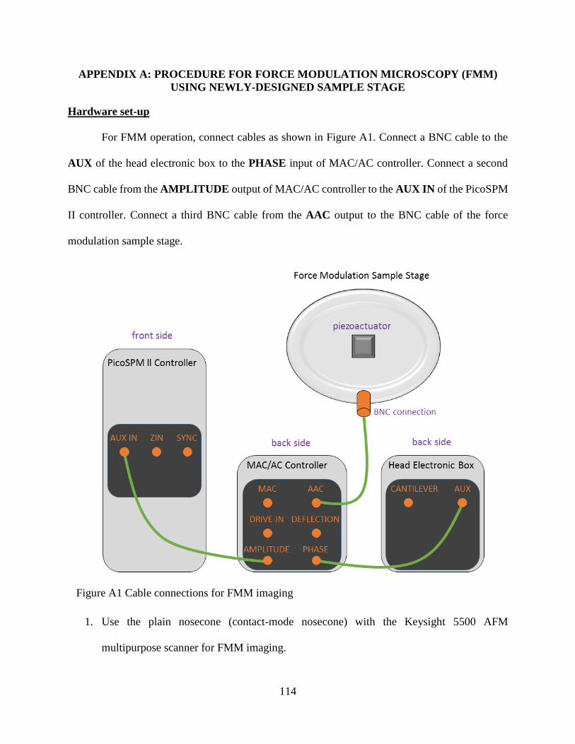
114
APPENDIX A: PROCEDURE FOR FORCE MODULATION MICROSCOPY (FMM)
USING NEWLY-DESIGNED SAMPLE STAGE
Hardware set-up
For FMM operation, connect cables as shown in Figure A1. Connect a BNC cable to the
AUX of the head electronic box to the PHASE input of MAC/AC controller. Connect a second
BNC cable from the AMPLITUDE output of MAC/AC controller to the AUX IN of the PicoSPM
II controller. Connect a third BNC cable from the AAC output to the BNC cable of the force
modulation sample stage.
1. Use the plain nosecone (contact-mode nosecone) with the Keysight 5500 AFM
multipurpose scanner for FMM imaging.
Figure A1 Cable connections for FMM imaging

115
2. Connect three cables between the PicoSPM II controller, MAC/AC controller, head
electronic box, and the FMM sample stage as shown in Figure A1.
3. Use silicon nitride cantilevers (MSCT, Bruker Probes) with force constants of 0.01-0.6
N/m for FMM imaging.
4. Put a magnet at the center of the FMM sample stage, then use double sided tape to glue the
sample on the magnet. Do not directly glue the sample on the sample stage.
5. Install the FMM sample stage and the scanner for FMM operation. Adjust the position of
laser and photodiode signal so that Deflection at -1 and LFM at 0 on the head electronic
box.
Software set-up
1. Launch the Picoview v1.12 software. Under main menu, select contact mode parameters
for Keysight 5500 AFM multipurpose scanner.
2. Create six channels on the second monitor including trace and retrace of topography, Aux
BNC (amplitude) and HEB Aux (phase) on the top/bottom row. Choose channels on the
top row to represent trace data and those on the bottom row to display retrace data.
3. Open the AFM AC Mode Tune window and set up the frequency range between 0 to 600
kHz.
4. Enter 0 for the Force Setpoint and then start to approach.
5. Under Control menu, select “advanced”, choose “AC mode”, Select AAC option in the
drive control window. Enable the Drive On and start the drive on percentage at 5%.

116
Frequency sweep
1. After the tip engages the surface, click on the Manual Tune button in the AC Tune
window to acquire a frequency spectrum with the vibration of the force modulation sample
stage.
2. Adjust the Drive On % until significant, detectable peaks are observed for the frequency
sweep (peak amplitude around 1 V). Save the frequency sweep as a *.txt file.
3. Choose the resonance frequencies in the frequency sweep by moving the red dash line on
top of the resonance peak maximum.
FMM imaging
1. Start to acquire FMM images and adjust the Integral (I) Gain, the Proportional (P) Gain,
the driving frequency and the Force Setpoint to tune the images.
2. During experiments, compare images and spectra with and without the field activated. Turn
the field on and off by enabling or disenabling the Drive On.
3. Try different resonance frequencies in the sweep and compare the FMM results.
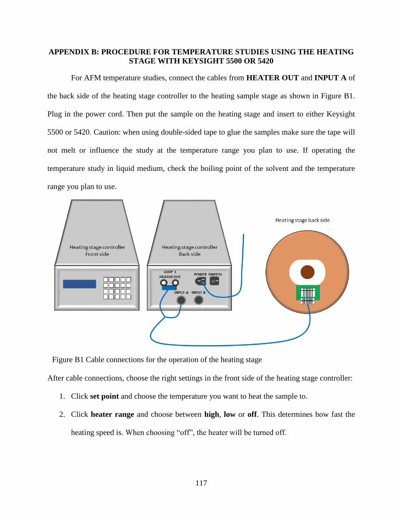
117
APPENDIX B: PROCEDURE FOR TEMPERATURE STUDIES USING THE HEATING
STAGE WITH KEYSIGHT 5500 OR 5420
For AFM temperature studies, connect the cables from HEATER OUT and INPUT A of
the back side of the heating stage controller to the heating sample stage as shown in Figure B1.
Plug in the power cord. Then put the sample on the heating stage and insert to either Keysight
5500 or 5420. Caution: when using double-sided tape to glue the samples make sure the tape will
not melt or influence the study at the temperature range you plan to use. If operating the
temperature study in liquid medium, check the boiling point of the solvent and the temperature
range you plan to use.
After cable connections, choose the right settings in the front side of the heating stage controller:
1. Click set point and choose the temperature you want to heat the sample to.
2. Click heater range and choose between high, low or off. This determines how fast the
heating speed is. When choosing “off”, the heater will be turned off.
Figure B1 Cable connections for the operation of the heating stage
118
3. Click Input setup, choose input A, type 100 Ω Plat/500, curve 06 PT-100, Filter on,
Filter points 08 and filter window 01%.
4. Click Display format, there are four locations we can set displays (two on the top and two
at bottom). At location 1, choose Display input A and Source Temp C; at location 2,
choose Display input B and Source Temp C; at location 3, choose Display setpoint; at
location 4, choose Display heater out.
5. Click Control setup, choose selected for loop 1, control with Input A, SP units Temp
C, Control mode open, power up enable, setpoint Ramp on, Ramp rate 100 K/m, and
heater load 50 Ω.
6. Click Interface, choose Baud 960, IEEE Address 12, and IEEE Term Cr Lf.
7. Click Zone setting, for loop 1, choose Zone 01, SP limit 0.000K, Prop (P) 50.00, Inteq
(I) 20.000, Drive (D) 0.00%.
8. If you want to turn off the heater during the experiment, click “heater off”.
119
APPENDIX C: SUPPLEMENTAL INFORMATION FOR THERMO-RESPONSIVE
BEHAVIOR OF LINEAR COPOLYPEPTOID NANOSTRUCTURES INVESTIGATED
WITH ATOMIC FORCE MICROSCOPY
1. Preparation of Nanopores within a Film of Octadecyltrichlorosilane (OTS)
Particle lithography was used to generate organosilane nanopatterns on Si(111) surfaces.
The silicon substrates were cleaned by immersion in piranha solution for 1.5 h. Piranha solution,
which is a mixture of sulfuric acid and hydrogen peroxide at a ratio of 3:1 (v/v), is highly corrosive
and should be handled cautiously. Substrates were then rinsed copiously with deionized water and
dried under argon. Monodisperse silica mesospheres (500 nm diameter) were washed with water
for three times by centrifugation to remove trace charge stabilizers or surfactants. The pellet of
silica mesospheres was resuspended in water by vortex mixing, and a drop (10 μL) was deposited
on a clean substrate. The sample was dried in air for 2 h to produce surface masks for further
chemical steps. As water evaporated during the drying step, capillary forces pull the mesospheres
together to form crystalline layers on flat surface. Next, the substrate was placed in an oven at 140
C for 24 h to temporarily anneal the mesospheres to the surface. After cooling, the sample was
immersed in a 0.1% solution of OTS (v/v) in toluene for 5 h. Next the sample was rinsed with
water and ethanol. To remove the mesoparticles, the substrate was sonicated for 15 min in ethanol
and water successively. The sample was dried under argon and characterized by atomic force
microscopy (AFM) with contact-mode in ambient air (Figure C1).
The hexagonal arrangement of the nanopores can be clearly seen in the 10 × 10 μm2
topography (Figure C1 a) and lateral force (Figure C1 b) images. The shapes of the nanopores are
more discernible is the zoom-in view (Figure C1 c). The chemistry difference of methyl terminated
silane and the bare Si substrate is distinguishable in the lateral force image (Figure C1 d). The
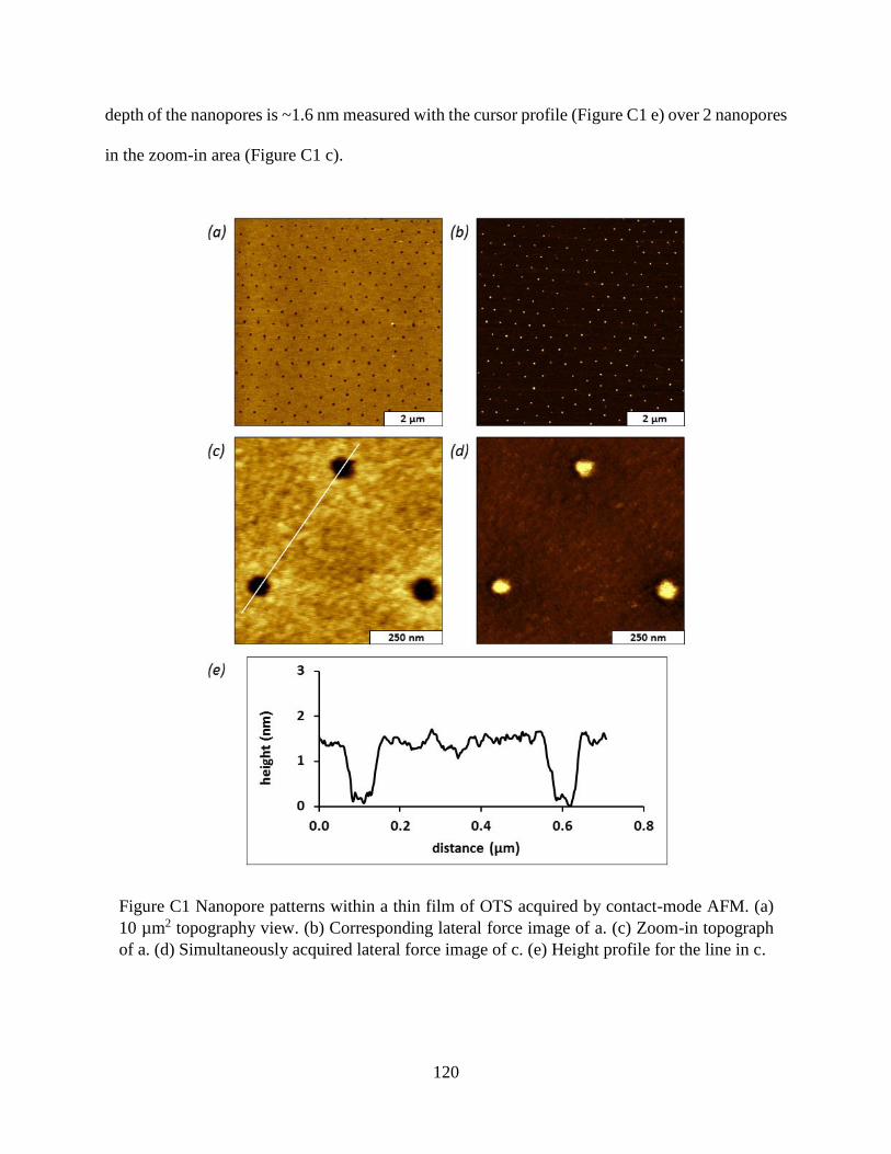
120
depth of the nanopores is ~1.6 nm measured with the cursor profile (Figure C1 e) over 2 nanopores
in the zoom-in area (Figure C1 c).
Figure C1 Nanopore patterns within a thin film of OTS acquired by contact-mode AFM. (a)
10 µm2 topography view. (b) Corresponding lateral force image of a. (c) Zoom-in topograph
of a. (d) Simultaneously acquired lateral force image of c. (e) Height profile for the line in c.
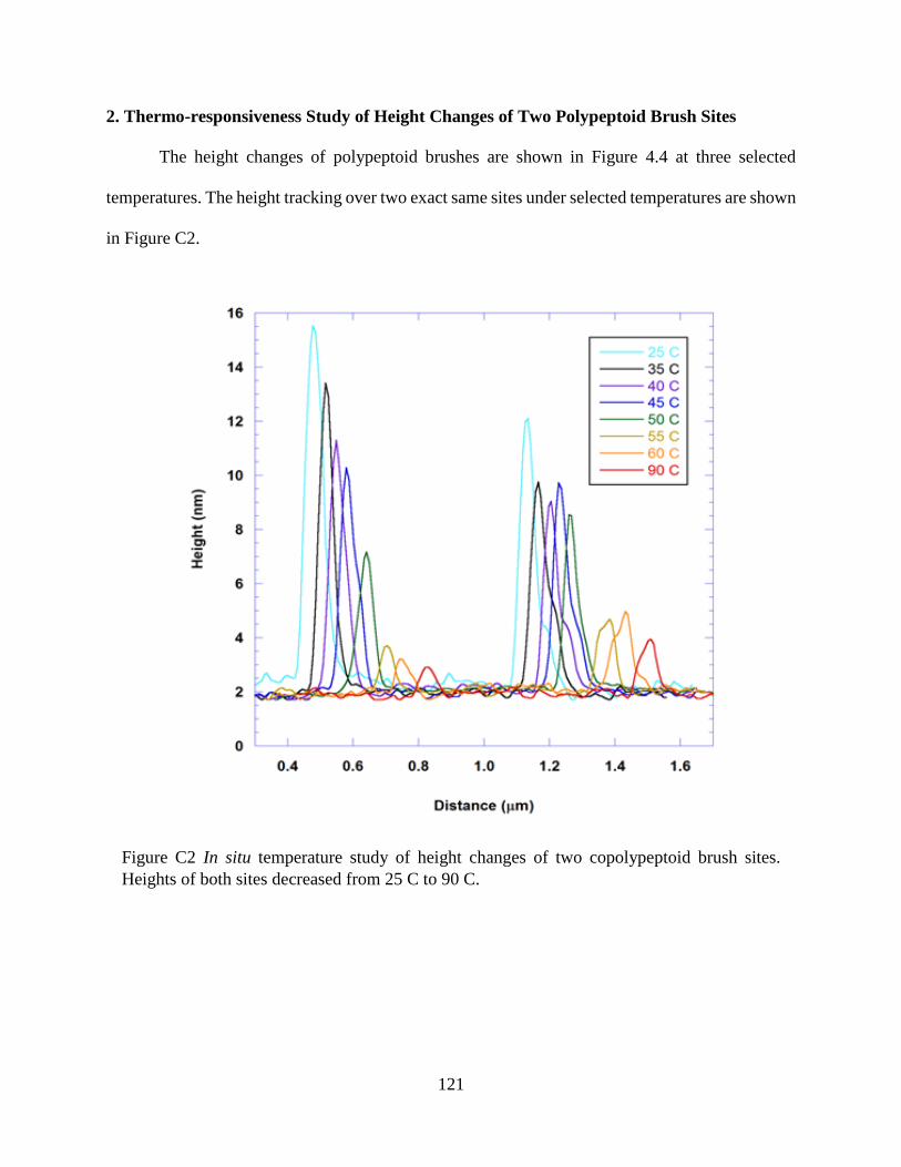
121
2. Thermo-responsiveness Study of Height Changes of Two Polypeptoid Brush Sites
The height changes of polypeptoid brushes are shown in Figure 4.4 at three selected
temperatures. The height tracking over two exact same sites under selected temperatures are shown
in Figure C2.
Figure C2 In situ temperature study of height changes of two copolypeptoid brush sites.
Heights of both sites decreased from 25 C to 90 C.
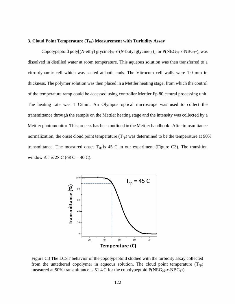
122
3. Cloud Point Temperature (Tcp) Measurement with Turbidity Assay
Copolypeptoid poly[(N-ethyl glycine)32-r-(N-butyl glycine17)], or P(NEG32-r-NBG17), was
dissolved in distilled water at room temperature. This aqueous solution was then transferred to a
vitro-dynamic cell which was sealed at both ends. The Vitrocom cell walls were 1.0 mm in
thickness. The polymer solution was then placed in a Mettler heating stage, from which the control
of the temperature ramp could be accessed using controller Mettler Fp 80 central processing unit.
The heating rate was 1 C/min. An Olympus optical microscope was used to collect the
transmittance through the sample on the Mettler heating stage and the intensity was collected by a
Mettler photomonitor. This process has been outlined in the Mettler handbook. After transmittance
normalization, the onset cloud point temperature (Tcp) was determined to be the temperature at 90%
transmittance. The measured onset Tcp is 45 C in our experiment (Figure C3). The transition
window ΔT is 28 C (68 C – 40 C).
Figure C3 The LCST behavior of the copolypeptoid studied with the turbidity assay collected
from the untethered copolymer in aqueous solution. The cloud point temperature (Tcp)
measured at 50% transmittance is 51.4 C for the copolypeptoid P(NEG32-r-NBG17).
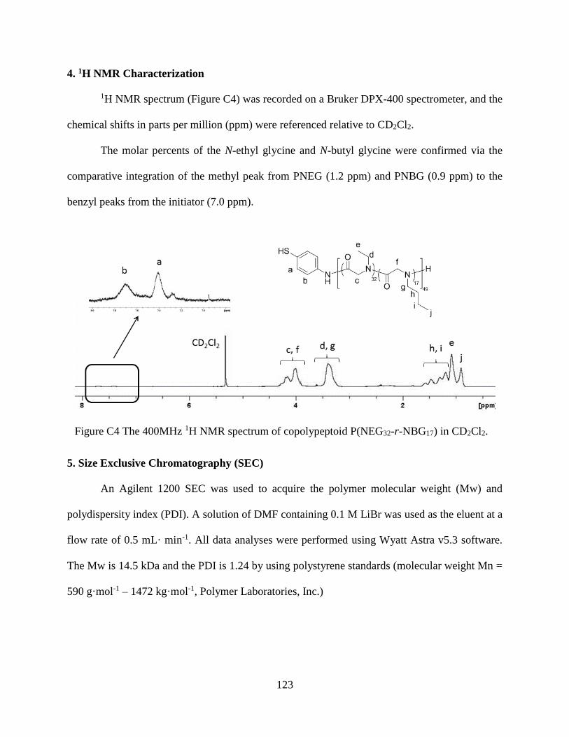
123
4. 1H NMR Characterization
1H NMR spectrum (Figure C4) was recorded on a Bruker DPX-400 spectrometer, and the
chemical shifts in parts per million (ppm) were referenced relative to CD2Cl2.
The molar percents of the N-ethyl glycine and N-butyl glycine were confirmed via the
comparative integration of the methyl peak from PNEG (1.2 ppm) and PNBG (0.9 ppm) to the
benzyl peaks from the initiator (7.0 ppm).
5. Size Exclusive Chromatography (SEC)
An Agilent 1200 SEC was used to acquire the polymer molecular weight (Mw) and
polydispersity index (PDI). A solution of DMF containing 0.1 M LiBr was used as the eluent at a
flow rate of 0.5 mL· min-1. All data analyses were performed using Wyatt Astra v5.3 software.
The Mw is 14.5 kDa and the PDI is 1.24 by using polystyrene standards (molecular weight Mn =
590 g·mol-1 – 1472 kg·mol-1, Polymer Laboratories, Inc.)
Figure C4 The 400MHz 1H NMR spectrum of copolypeptoid P(NEG32-r-NBG17) in CD2Cl2.
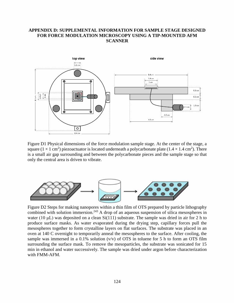
124
APPENDIX D: SUPPLEMENTAL INFORMATION FOR SAMPLE STAGE DESIGNED
FOR FORCE MODULATION MICROSCOPY USING A TIP-MOUNTED AFM
SCANNER
Figure D1 Physical dimensions of the force modulation sample stage. At the center of the stage, a
square (1 × 1 cm2) piezoactuator is located underneath a polycarbonate plate (1.4 × 1.4 cm2). There
is a small air gap surrounding and between the polycarbonate pieces and the sample stage so that
only the central area is driven to vibrate.
Figure D2 Steps for making nanopores within a thin film of OTS prepared by particle lithography
combined with solution immersion.243 A drop of an aqueous suspension of silica mesospheres in
water (10 μL) was deposited on a clean Si(111) substrate. The sample was dried in air for 2 h to
produce surface masks. As water evaporated during the drying step, capillary forces pull the
mesospheres together to form crystalline layers on flat surfaces. The substrate was placed in an
oven at 140 C overnight to temporarily anneal the mesospheres to the surface. After cooling, the
sample was immersed in a 0.1% solution (v/v) of OTS in toluene for 5 h to form an OTS film
surrounding the surface mask. To remove the mesoparticles, the substrate was sonicated for 15
min in ethanol and water successively. The sample was dried under argon before characterization
with FMM-AFM.
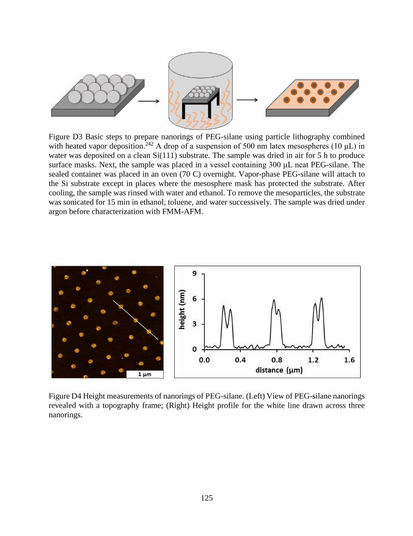
125
Figure D3 Basic steps to prepare nanorings of PEG-silane using particle lithography combined
with heated vapor deposition.242 A drop of a suspension of 500 nm latex mesospheres (10 μL) in
water was deposited on a clean Si(111) substrate. The sample was dried in air for 5 h to produce
surface masks. Next, the sample was placed in a vessel containing 300 μL neat PEG-silane. The
sealed container was placed in an oven (70 C) overnight. Vapor-phase PEG-silane will attach to
the Si substrate except in places where the mesosphere mask has protected the substrate. After
cooling, the sample was rinsed with water and ethanol. To remove the mesoparticles, the substrate
was sonicated for 15 min in ethanol, toluene, and water successively. The sample was dried under
argon before characterization with FMM-AFM.
Figure D4 Height measurements of nanorings of PEG-silane. (Left) View of PEG-silane nanorings
revealed with a topography frame; (Right) Height profile for the white line drawn across three
nanorings.
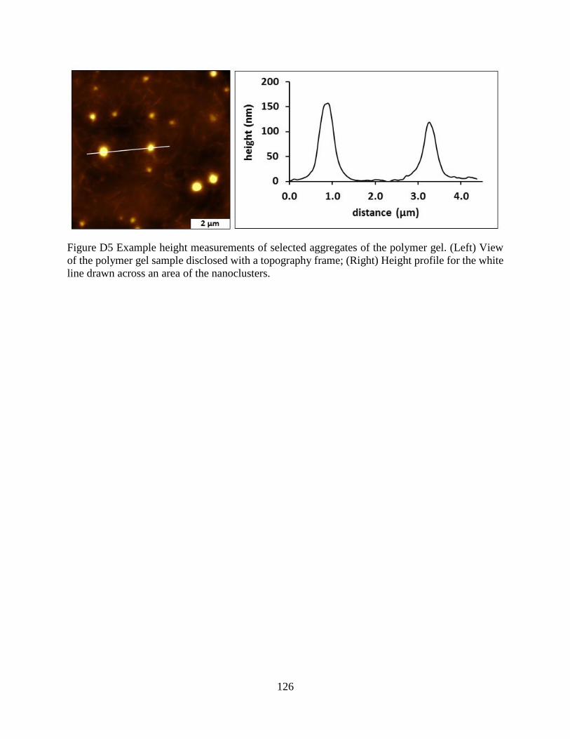
126
Figure D5 Example height measurements of selected aggregates of the polymer gel. (Left) View
of the polymer gel sample disclosed with a topography frame; (Right) Height profile for the white
line drawn across an area of the nanoclusters.
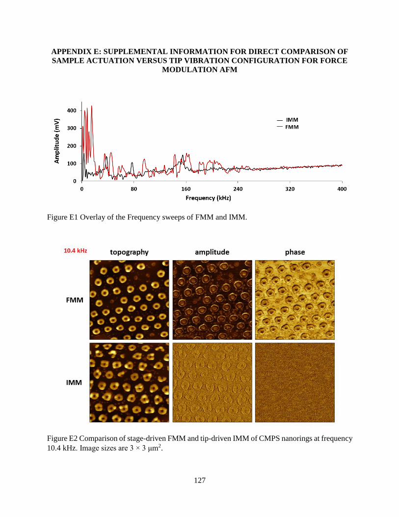
127
APPENDIX E: SUPPLEMENTAL INFORMATION FOR DIRECT COMPARISON OF
SAMPLE ACTUATION VERSUS TIP VIBRATION CONFIGURATION FOR FORCE
MODULATION AFM
Figure E1 Overlay of the Frequency sweeps of FMM and IMM.
Figure E2 Comparison of stage-driven FMM and tip-driven IMM of CMPS nanorings at frequency
10.4 kHz. Image sizes are 3 × 3 μm2.
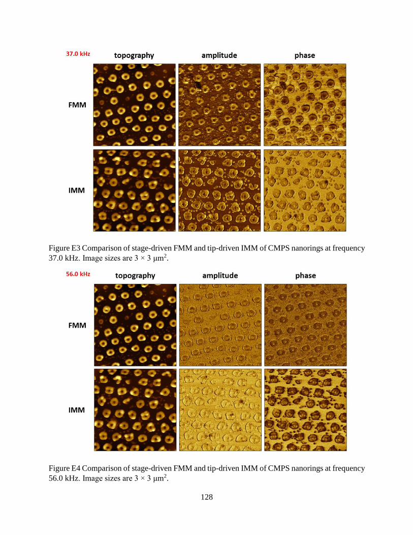
128
Figure E3 Comparison of stage-driven FMM and tip-driven IMM of CMPS nanorings at frequency
37.0 kHz. Image sizes are 3 × 3 μm2.
Figure E4 Comparison of stage-driven FMM and tip-driven IMM of CMPS nanorings at frequency
56.0 kHz. Image sizes are 3 × 3 μm2.
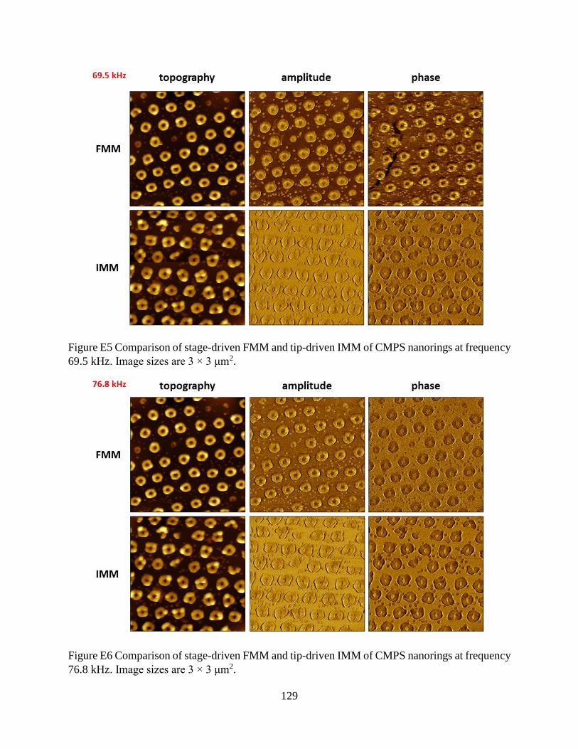
129
Figure E5 Comparison of stage-driven FMM and tip-driven IMM of CMPS nanorings at frequency
69.5 kHz. Image sizes are 3 × 3 μm2.
Figure E6 Comparison of stage-driven FMM and tip-driven IMM of CMPS nanorings at frequency
76.8 kHz. Image sizes are 3 × 3 μm2.
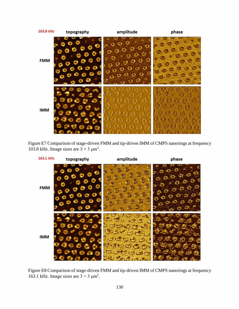
130
Figure E7 Comparison of stage-driven FMM and tip-driven IMM of CMPS nanorings at frequency
103.8 kHz. Image sizes are 3 × 3 μm2.
Figure E8 Comparison of stage-driven FMM and tip-driven IMM of CMPS nanorings at frequency
163.1 kHz. Image sizes are 3 × 3 μm2.
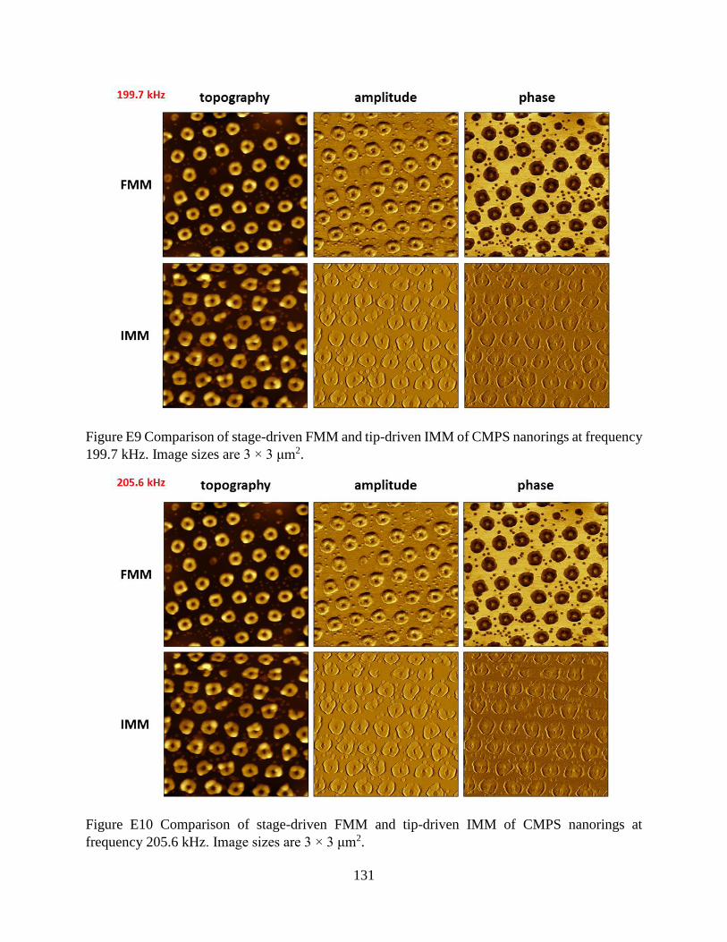
131
Figure E9 Comparison of stage-driven FMM and tip-driven IMM of CMPS nanorings at frequency
199.7 kHz. Image sizes are 3 × 3 μm2.
Figure E10 Comparison of stage-driven FMM and tip-driven IMM of CMPS nanorings at
frequency 205.6 kHz. Image sizes are 3 × 3 μm2.
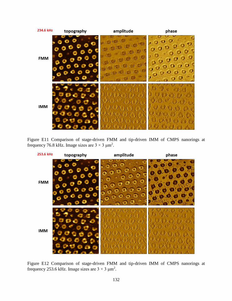
132
Figure E11 Comparison of stage-driven FMM and tip-driven IMM of CMPS nanorings at
frequency 76.8 kHz. Image sizes are 3 × 3 μm2.
Figure E12 Comparison of stage-driven FMM and tip-driven IMM of CMPS nanorings at
frequency 253.6 kHz. Image sizes are 3 × 3 μm2.
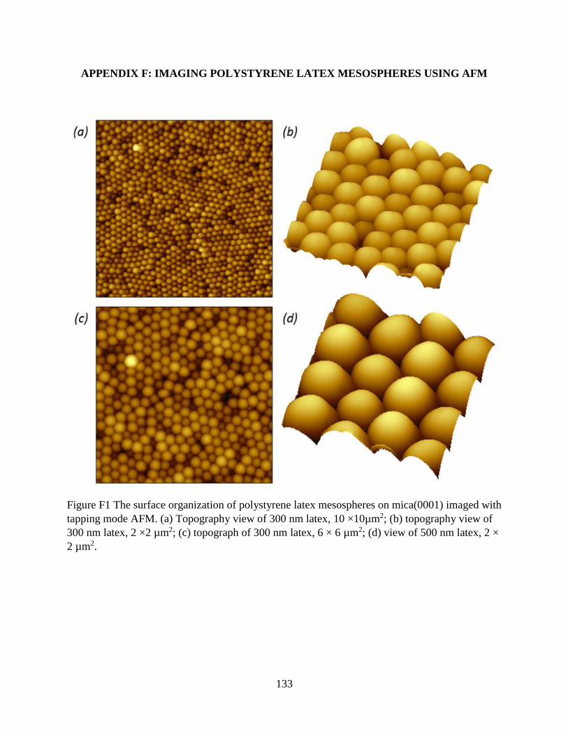
133
APPENDIX F: IMAGING POLYSTYRENE LATEX MESOSPHERES USING AFM
Figure F1 The surface organization of polystyrene latex mesospheres on mica(0001) imaged with
tapping mode AFM. (a) Topography view of 300 nm latex, 10 ×10µm2; (b) topography view of
300 nm latex, 2 ×2 µm2; (c) topograph of 300 nm latex, 6 × 6 µm2; (d) view of 500 nm latex, 2 ×
2 µm2.
134
APPENDIX F: PERMISSIONS

135

136
137
138
VITA
Lu Lu was born and grew up in Lanzhou, China. She earned her Bachelor of Science degree
in polymer science and engineering department from University of Science and Technology
(USTC) of China in 2010. During her time in USTC, she participated in undergraduate research
under Dr. Ruke Bai for a year and published a co-authored journal article. She joined Chemistry
department at Louisiana State University (LSU) in the Fall of 2010. She is a Ph.D candidate in the
fields of analytical and macromolecular chemistry under the supervision of Dr. Jayne C. Garno
and Dr. Donghui Zhang. Her research interests include: preparing patterns of polymer brushes on
surfaces, studying the thermo-responsive properties of patterned polymer nanobrushes using
atomic force microscopy (AFM) and developing sample stage accessories with AFM for force
modulation microscopy studies. Thus far at LSU, Lu submitted one first author journal articles and
published five collaborative research papers. She had four more first author and several shared
manuscripts which are under preparation. Lu presented her research at both regional and national
conferences including one talk, five first-author posters and four co-authored posters. Lu also gave
a talk in the workshop held by Keysight Technologies at LSU. Lu directed senior thesis research
for an undergraduate student at LSU, whose name is Rasheda Gros. Rasheda won a poster award
in 2014 Annual Biomedical Research Conference for Minority Students (ABRCMS) for her
studies with AFM investigations of nanopatterns prepared with organosilane and nanoparticles.