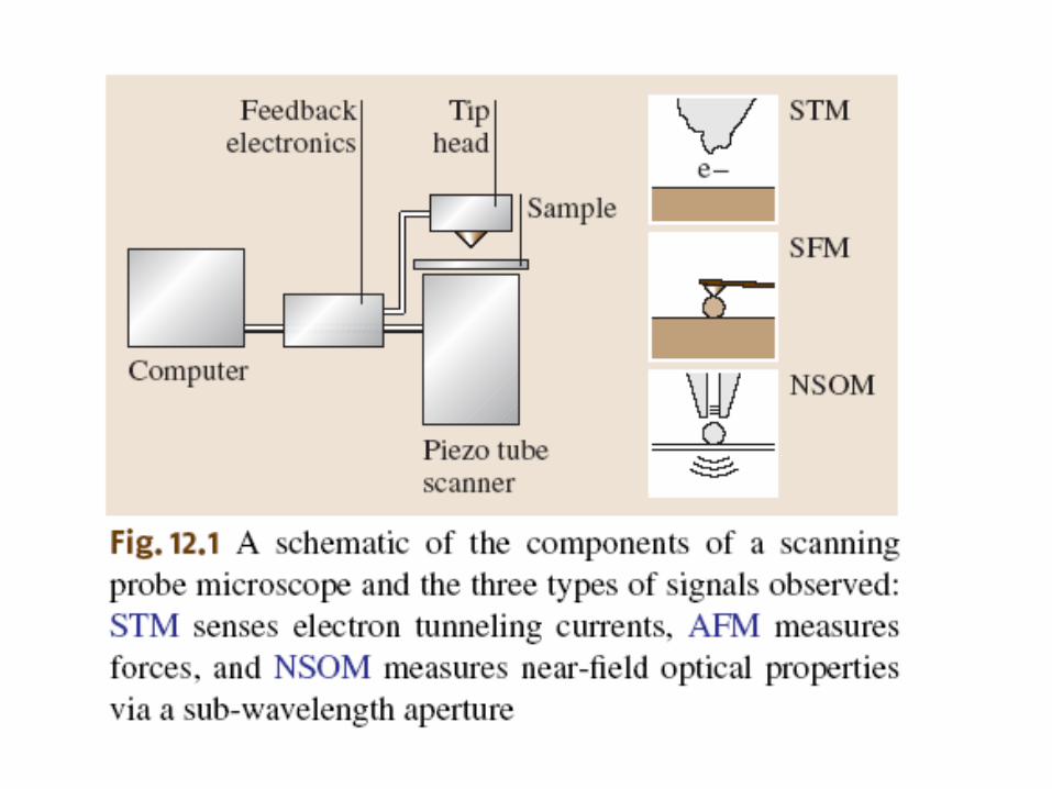
scanning probe microscopy – principle of operation, instrumentation, and probes
TRANSCRIPT
Scanning Probe Microscopy – Principle of Operation,
Instrumentation, and Probes

• The principle of electron tunneling was proposed by Giaever. He envisioned that if a potential difference is applied to two metals separated by a thin insulating film, a current will flow because of the ability of electrons to penetrate a potential barrier.
• R. Young developed field emission topograph profiler.
• Binnig and Rohler introduced vacuum tunneling combined with lateral scanning. The vacuum provides the ideal barrier for tunneling. The lateral scanning allows one to image surfaces with exquisite resolution, lateral-less than 1 nm and vertical-less than 0.1 nm, sufficient to define the position of single atoms.
Scanning Probe Microscopy-STM
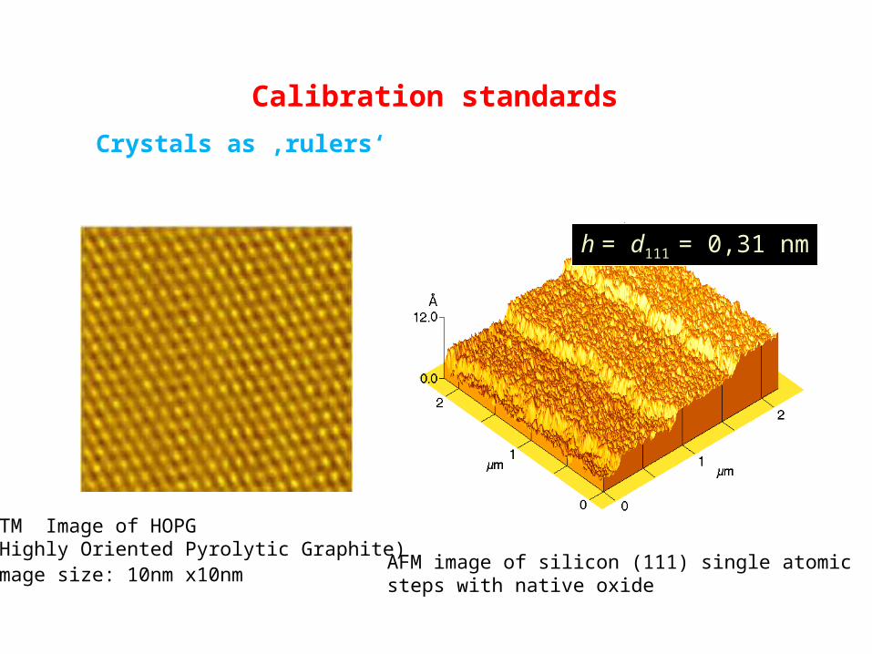
h = d111 = 0,31 nm
AFM image of silicon (111) single atomicsteps with native oxide
STM Image of HOPG (Highly Oriented Pyrolytic Graphite)Image size: 10nm x10nm
Crystals as ‚rulers‘
Calibration standards
Since the introduction of the STM in 1981 and AFM in 1985 by Binnig and Rohler , many variations of probe based microscopies, referred to as SPMs,
have been developed.
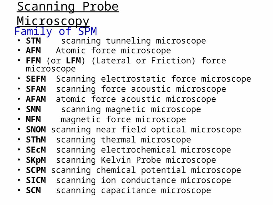
Scanning Probe Microscopy
• STM scanning tunneling microscope • AFM Atomic force microscope • FFM (or LFM) (Lateral or Friction) force microscope• SEFM Scanning electrostatic force microscope• SFAM scanning force acoustic microscope• AFAM atomic force acoustic microscope• SMM scanning magnetic microscope • MFM magnetic force microscope• SNOM scanning near field optical microscope• SThM scanning thermal microscope• SEcM scanning electrochemical microscope• SKpM scanning Kelvin Probe microscope• SCPM scanning chemical potential microscope• SICM scanning ion conductance microscope• SCM scanning capacitance microscope
Family of SPM
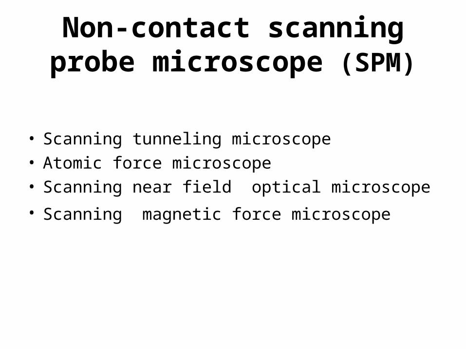
Non-contact scanning probe microscope (SPM)
• Scanning tunneling microscope• Atomic force microscope• Scanning near field optical microscope
• Scanning magnetic force microscope
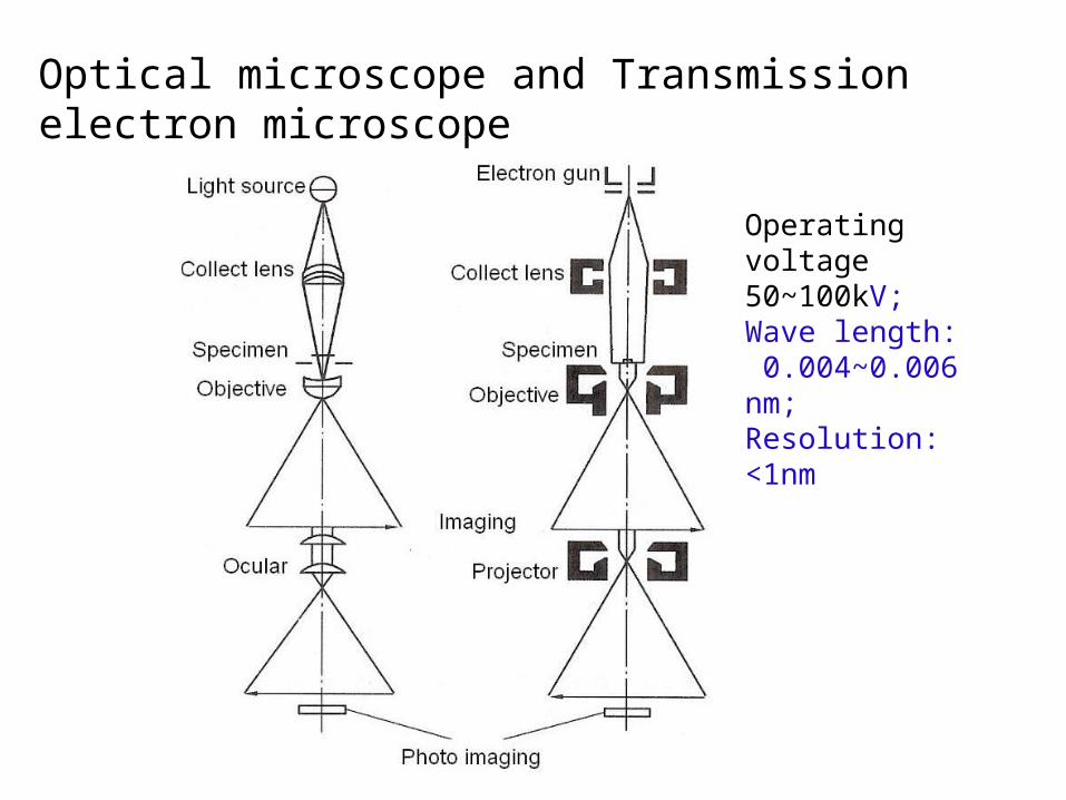
Optical microscope and Transmission electron microscope
Operating voltage 50~100kV;Wave length: 0.004~0.006 nm;Resolution: <1nm
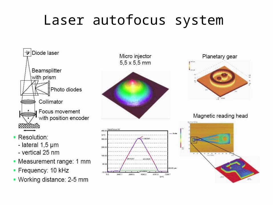
Laser autofocus system
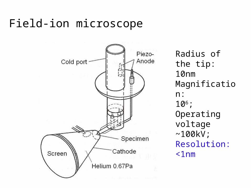
Field-ion microscope
Radius of the tip: 10nmMagnification:106;Operating voltage ~100kV;Resolution: <1nm
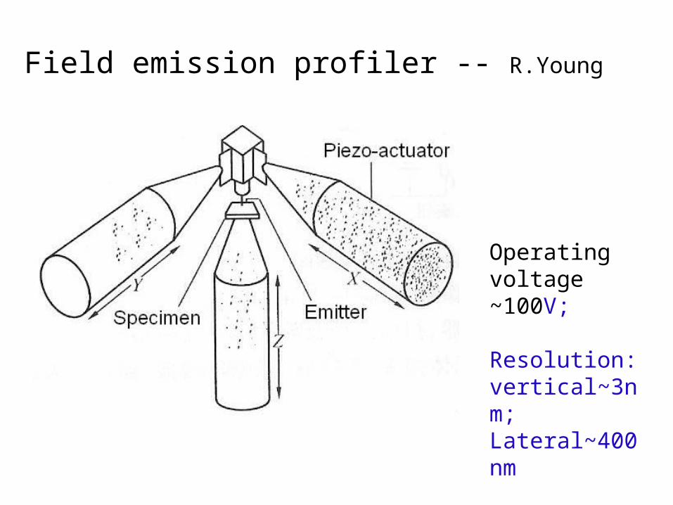
Field emission profiler -- R.Young
Operating voltage ~100V;
Resolution: vertical~3nm;Lateral~400nm

JT ― the tunnel current, a sensitive function of the gap width d ;VT ― the bias voltage;φ― the average barrier height (work function) ; A ― constant = 1.025 eV−1/2 Å−1.
With a work function of a few eV, JT changes by an order of magnitude for every angstrom change of d.
Principle of operation of the STM made by Binnig and Rohrer
JT ∝ VT exp(−Aφ1/2d)
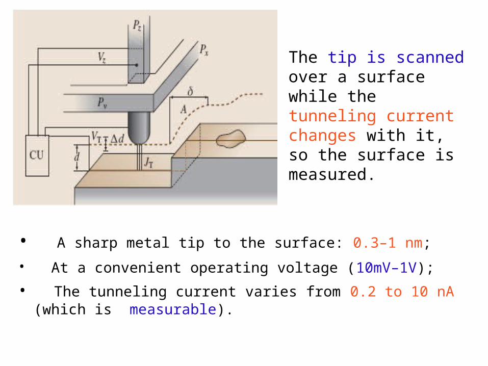
• A sharp metal tip to the surface: 0.3–1 nm;
• At a convenient operating voltage (10mV–1V); • The tunneling current varies from 0.2 to 10 nA (which is
measurable).
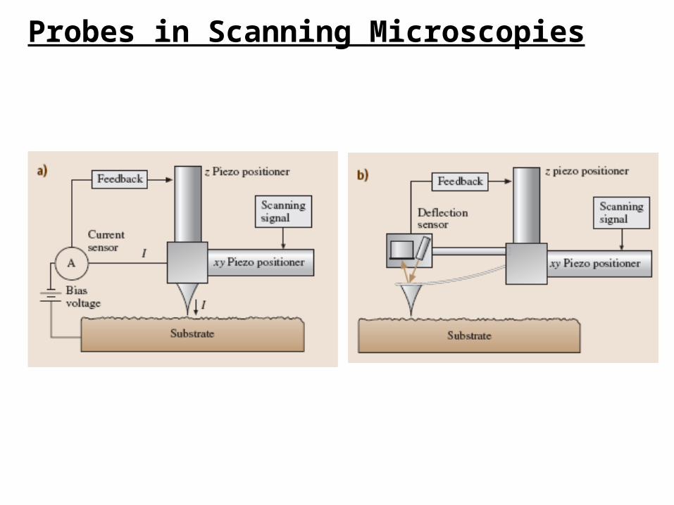
The tip is scanned over a surface while the tunneling current changes with it, so the surface is measured.

• the head which houses the piezoelectric tube scanner for three dimensional motion of the tip and • the preamplifier circuit (FET input amplifier)
mounted on top of the head for the tunneling current,
• the base on which the sample is mounted, and the base support, which supports the base and head
Nanoscope STM consists of three main parts:

Principle of operation of a commercial STM, a sharp tip attached to a piezoelectric tube scanner is scanned on a sample
Scanning Probe Microscopy-STM
The motion of the tip due to external vibrations is proportional to the square of the ratio of vibration frequency to the resonant frequency of the tube. Therefore, to minimize the tip vibrations, the resonant frequencies of the tube are high at about 60 kHz in the vertical direction and about 40 kHz in the horizontal direction.
Scanning Probe Microscopy-STM
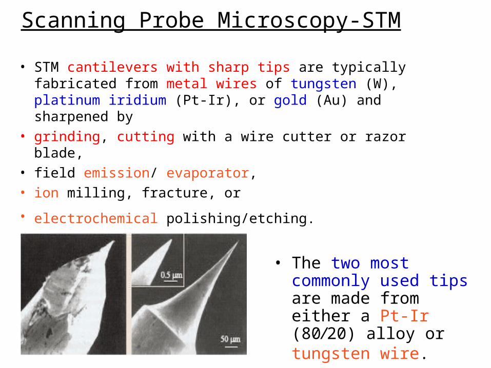
• STM cantilevers with sharp tips are typically fabricated from metal wires of tungsten (W), platinum iridium (Pt-Ir), or gold (Au) and sharpened by
• grinding, cutting with a wire cutter or razor blade, • field emission/ evaporator, • ion milling, fracture, or
• electrochemical polishing/etching.
• The two most commonly used tips are made from either a Pt-Ir (80/20) alloy or tungsten wire.

Schematic of a typical tungsten cantilever with a sharp tip produced by electrochemical etching.
A lateral resolution of about 2 nm requires tip radii on the order of 10 nm.
The resonant frequencies of the tube are high at about 60 kHz in the vertical direction and about 40 kHz in the horizontal direction.
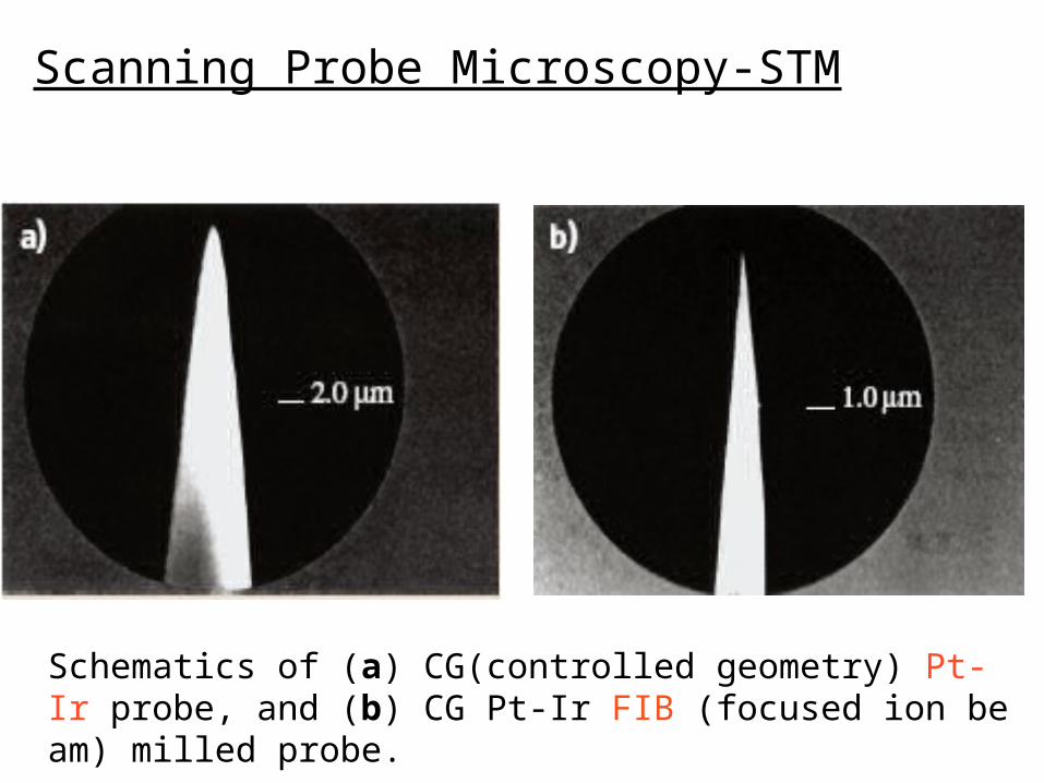
Schematics of (a) CG(controlled geometry) Pt-Ir probe, and (b) CG Pt-Ir FIB (focused ion beam) milled probe.
Scanning Probe Microscopy-STM

STM can be operated in either the constant-current or the constant height mode. The images are of graphite in air.
Constant-current mode: a feedback network changes the height of thetip z to keep the current constant. → topographic map yielded by the displacement of the tip.
Constant height mode: a metal tip scannes across a surface at nearly constant height and constant voltage while the current is monitored → topographic map yielded
by the change of the current.
Scanning Probe Microscopy-STM
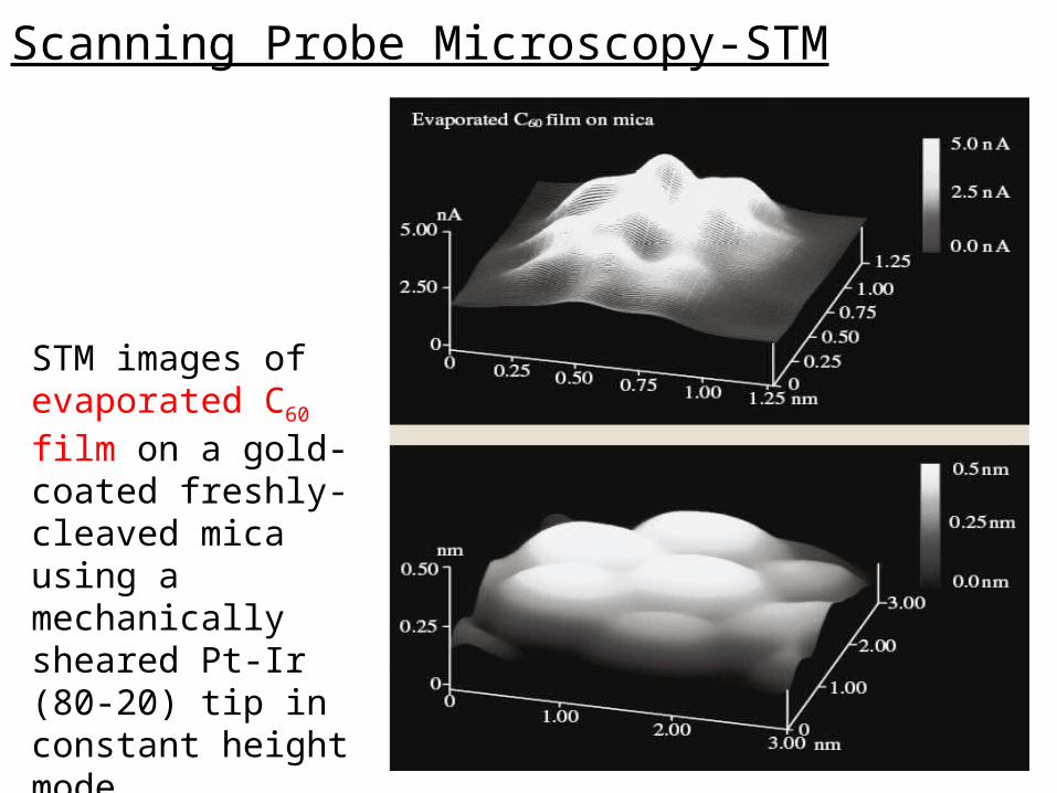
STM images of evaporated C60 film on a gold-coated freshly-cleaved mica using a mechanically sheared Pt-Ir (80-20) tip in constant height mode.
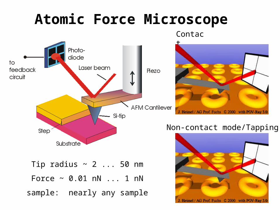
Atomic Force Microscope
Tip radius ~ 2 ... 50 nm
Force ~ 0.01 nN ... 1 nN
sample: nearly any sample
Contact
Non-contact mode/Tapping
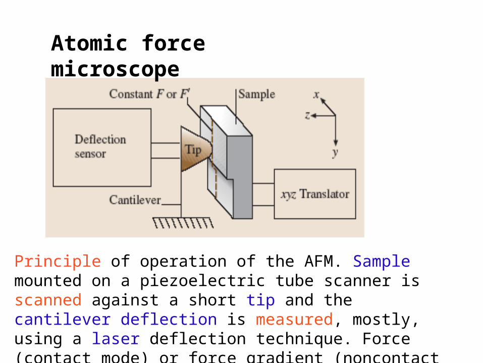
Principle of operation of the AFM. Sample mounted on a piezoelectric tube scanner is scanned against a short tip and the cantilever deflection is measured, mostly, using a laser deflection technique. Force (contact mode) or force gradient (noncontact mode) is measured during scanning.
Atomic force microscope
Atomic force microscope
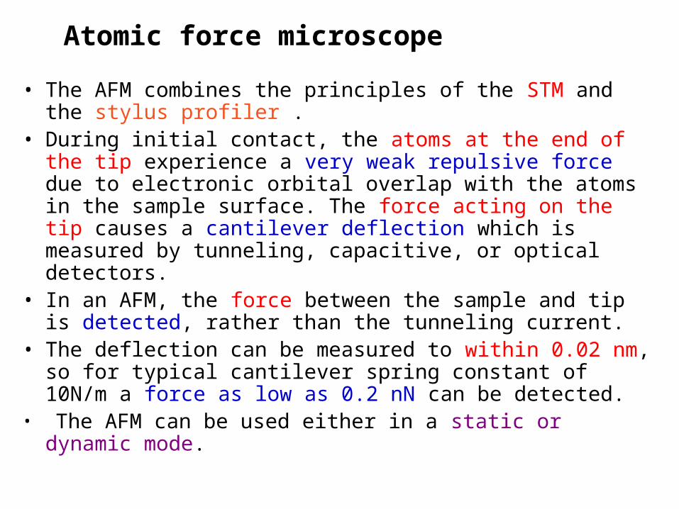
• The AFM combines the principles of the STM and the stylus profiler .
• During initial contact, the atoms at the end of the tip experience a very weak repulsive force due to electronic orbital overlap with the atoms in the sample surface. The force acting on the tip causes a cantilever deflection which is measured by tunneling, capacitive, or optical detectors.
• In an AFM, the force between the sample and tip is detected, rather than the tunneling current.
• The deflection can be measured to within 0.02 nm, so for typical cantilever spring constant of 10N/m a force as low as 0.2 nN can be detected.
• The AFM can be used either in a static or dynamic mode.
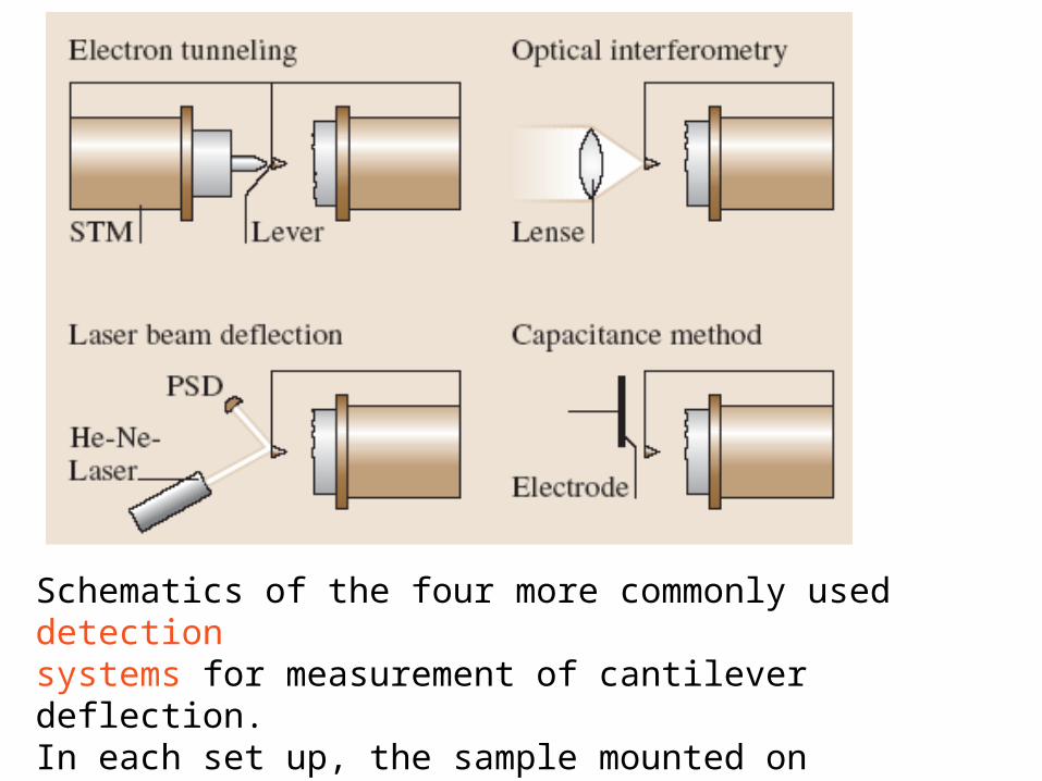
Schematics of the four more commonly used detectionsystems for measurement of cantilever deflection.In each set up, the sample mounted on piezoelectric bodyis shown on the right, the cantilever in the middle, and thecorresponding deflection sensor on the left
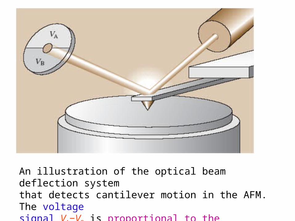
An illustration of the optical beam deflection systemthat detects cantilever motion in the AFM. The voltagesignal VA−VB is proportional to the deflection
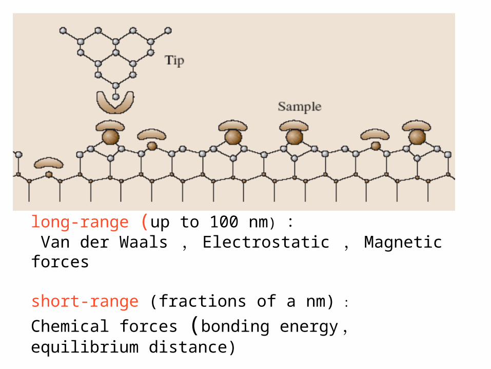
long-range (up to 100 nm) : Van der Waals , Electrostatic , Magnetic forces
short-range (fractions of a nm) :
Chemical forces (bonding energy , equilibrium distance)
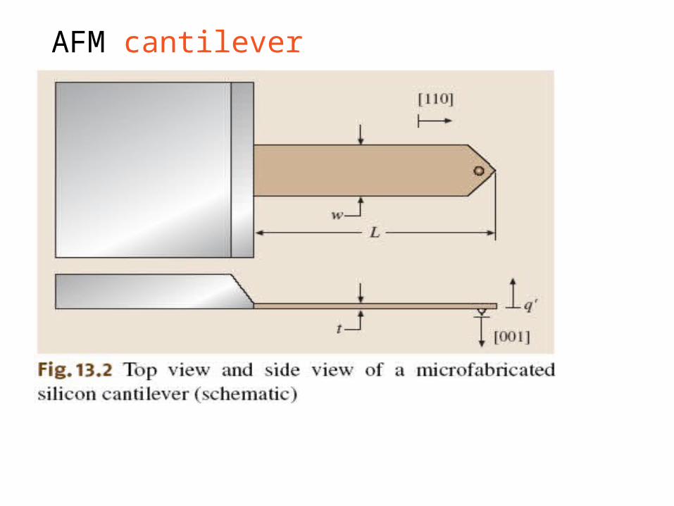
AFM cantilever
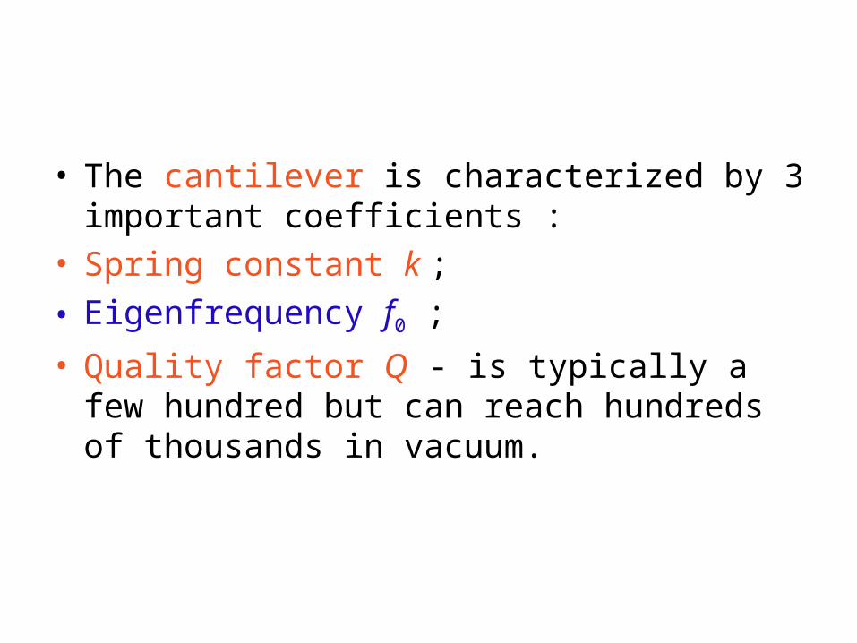
• The cantilever is characterized by 3 important coefficients :
• Spring constant k ;
• Eigenfrequency f0 ;
• Quality factor Q - is typically a few hundred but can reach hundreds of thousands in vacuum.
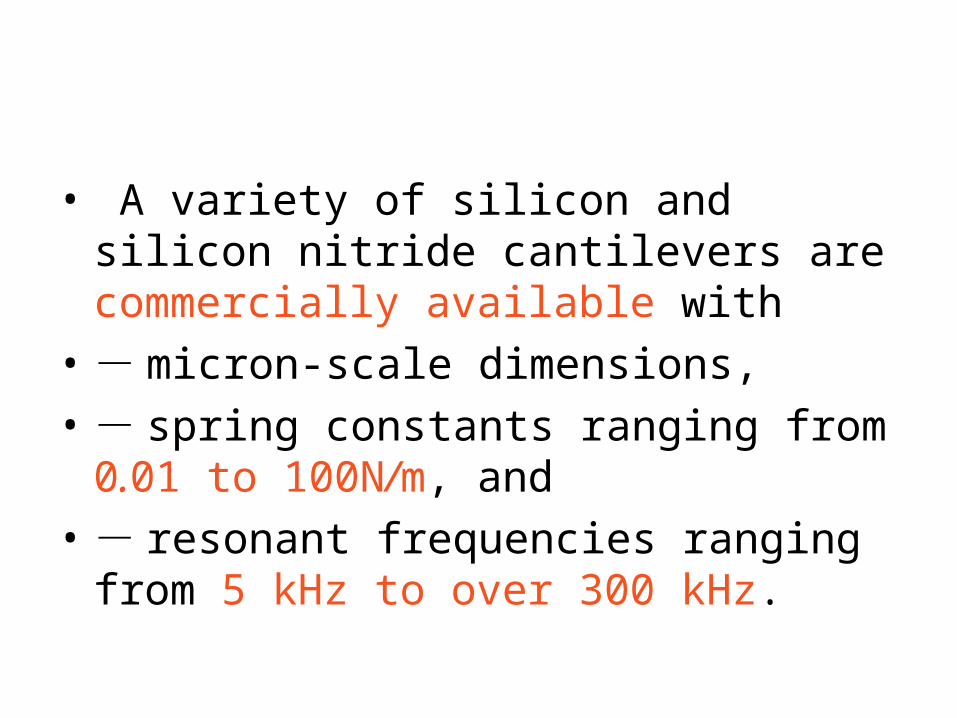
• A variety of silicon and silicon nitride cantilevers are commercially available with
• - micron-scale dimensions,
• - spring constants ranging from 0.01 to 100N/m, and
• - resonant frequencies ranging from 5 kHz to over 300 kHz.

Spring constant of cantilever
• The vibration frequencies ω of atoms bound in a molecule or in a crystalline solid are typically 1013 Hz or higher;
• The mass of the atoms m on the order of 10−25;• Interatomic spring constants k, given by ω2m, on the
order of 10N/m. • Therefore, a cantilever beam with a spring constant of
about 1N/m or lower is desirable.
To obtain atomic resolution with the AFM, the spring constant of the cantilever should be weaker than the equivalent spring between atoms.
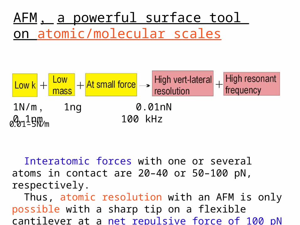
AFM , a powerful surface tool on atomic/molecular scales
1N/m , 1ng 0.01nN 0.1nm 100 kHz
Interatomic forces with one or several atoms in contact are 20–40 or 50–100 pN, respectively. Thus, atomic resolution with an AFM is only possible with a sharp tip on a flexible cantilever at a net repulsive force of 100 pN or lower.
0.01–5N/m

Contact (static) Mode In the contact (static) mode, the interaction force between tip and sample is measured by measuring the cantilever deflection. Tip approach sample: A-B-C
A-B ― <10-10N (attractive force); B-C ― >10-10N (repulsive force);
Tip leaves sample: C-B-D-A
C-B ― > 10-10N (repulsive force); B-D ― <10-10N (attractive force); D-A ― <10-10N (repulsive force);

NonContact (dynamic) Mode
q´(t) ― the deflection of the tip of the cantilever, It oscillates with anamplitude A at a distance q(t) to a sample.
kts varies in orders of magnitude during one oscillation cycle,

NonContact (static) Mode
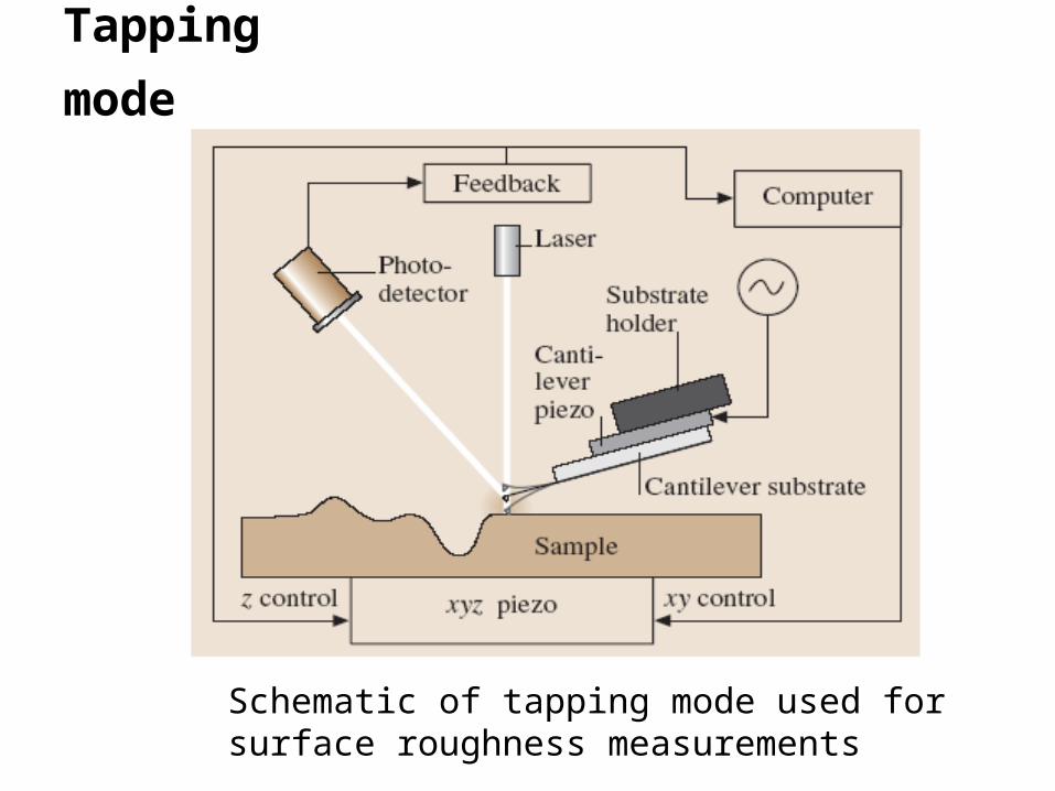
Schematic of tapping mode used for surface roughness measurements
Tapping mode
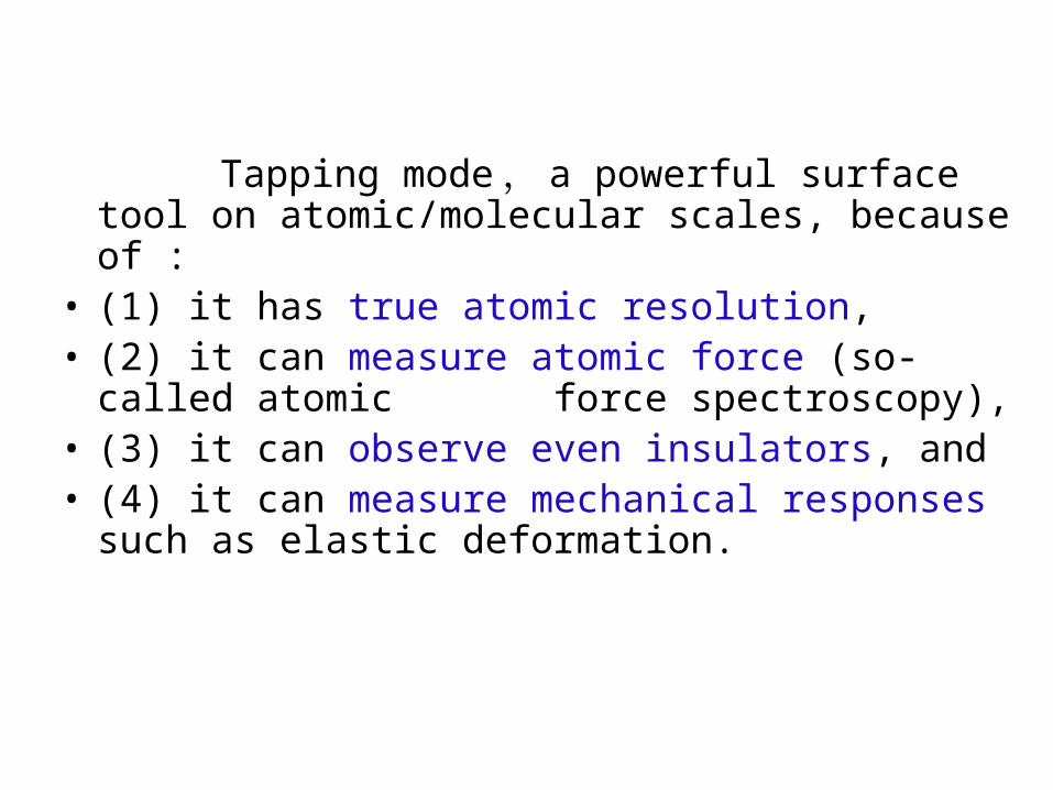
Tapping mode , a powerful surface tool on atomic/molecular scales, because of :
• (1) it has true atomic resolution,• (2) it can measure atomic force (so-called atomic
force spectroscopy), • (3) it can observe even insulators, and • (4) it can measure mechanical responses such as
elastic deformation.
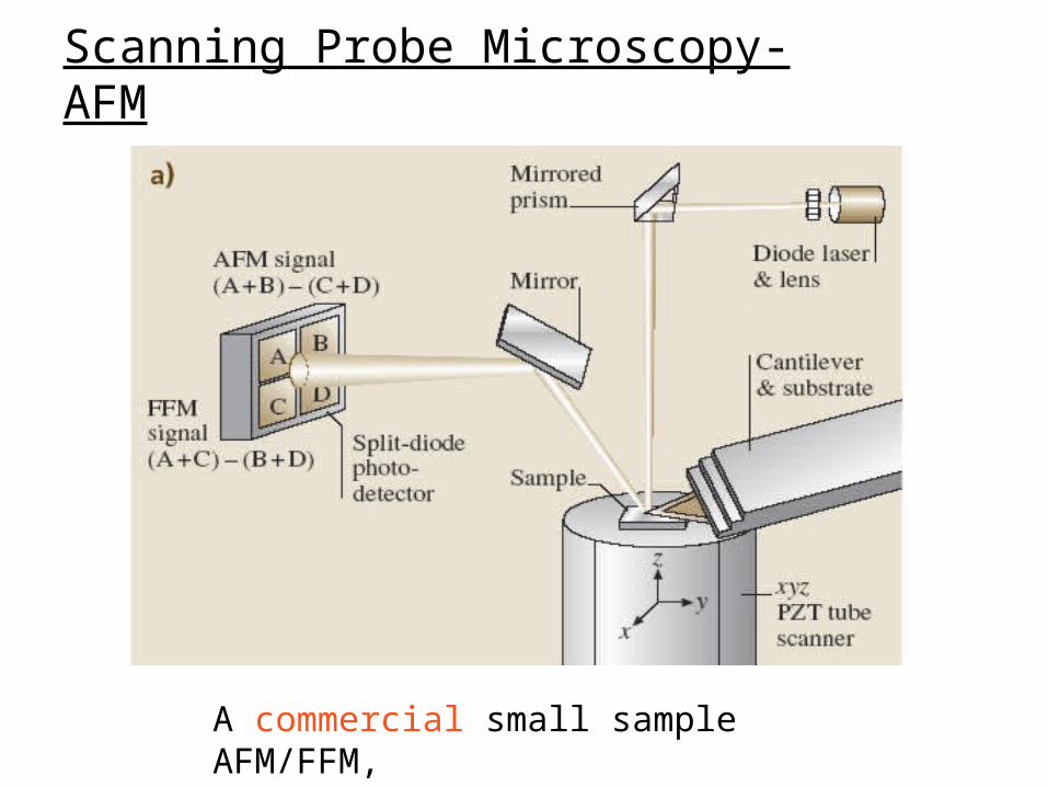
Scanning Probe Microscopy-AFM
A commercial small sample AFM/FFM,
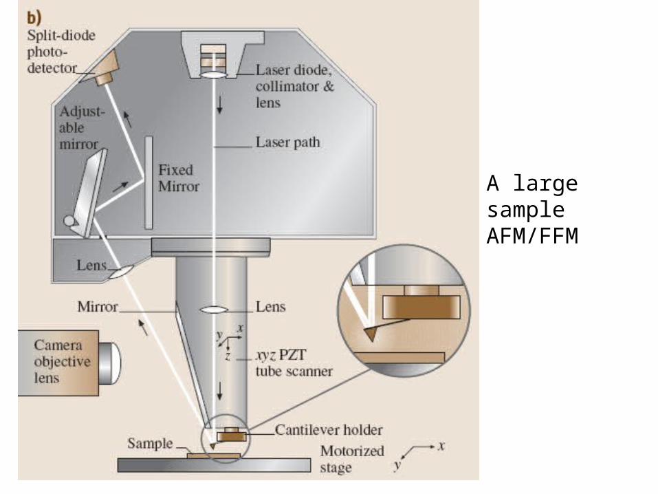
A large sample AFM/FFM
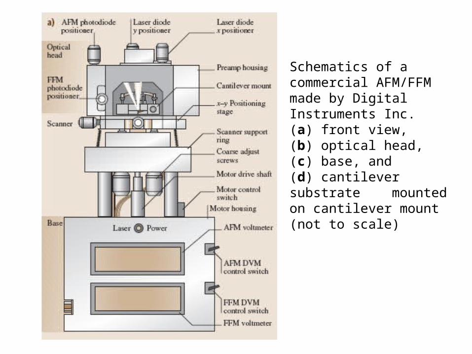
Schematics of a commercial AFM/FFM made by Digital Instruments Inc. (a) front view, (b) optical head, (c) base, and (d) cantilever substrate mounted on cantilever mount (not to scale)
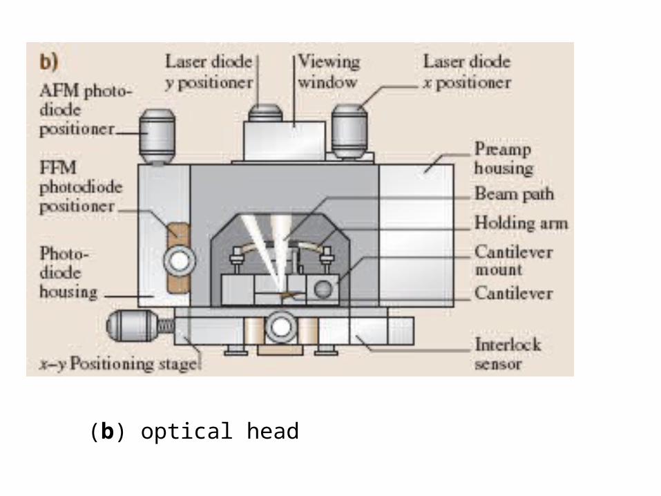
(b) optical head
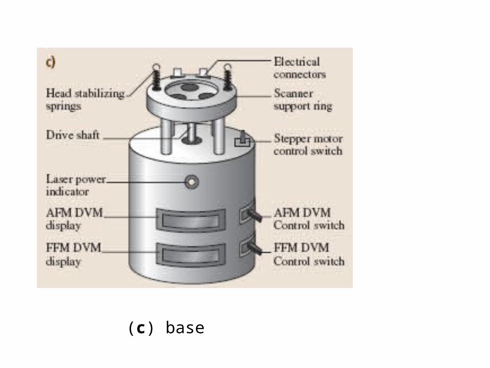
(c) base
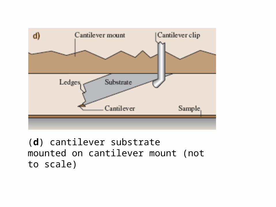
(d) cantilever substrate mounted on cantilever mount (not to scale)
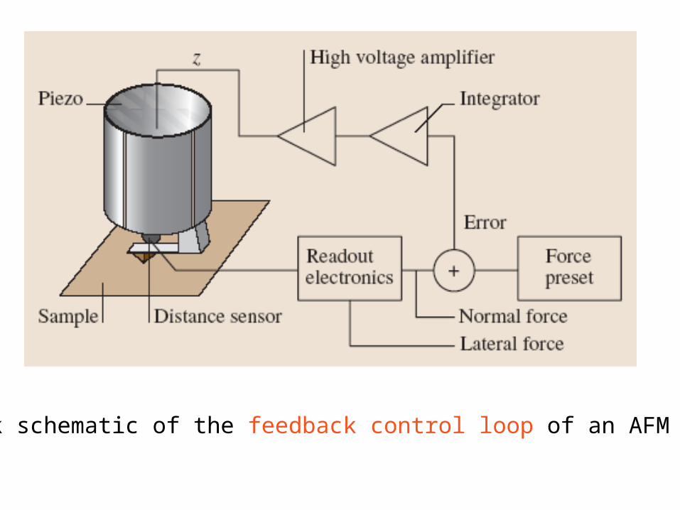
Block schematic of the feedback control loop of an AFM
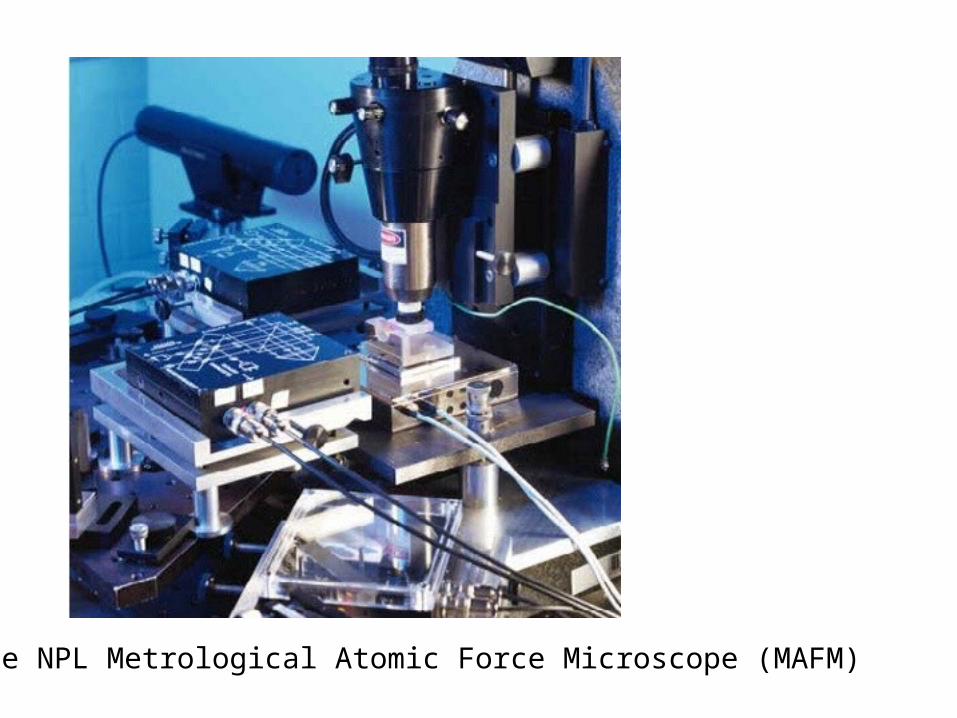
The NPL Metrological Atomic Force Microscope (MAFM)
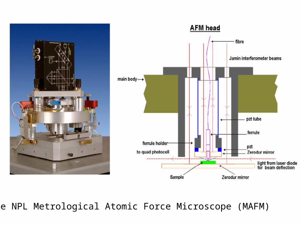
The NPL Metrological Atomic Force Microscope (MAFM)
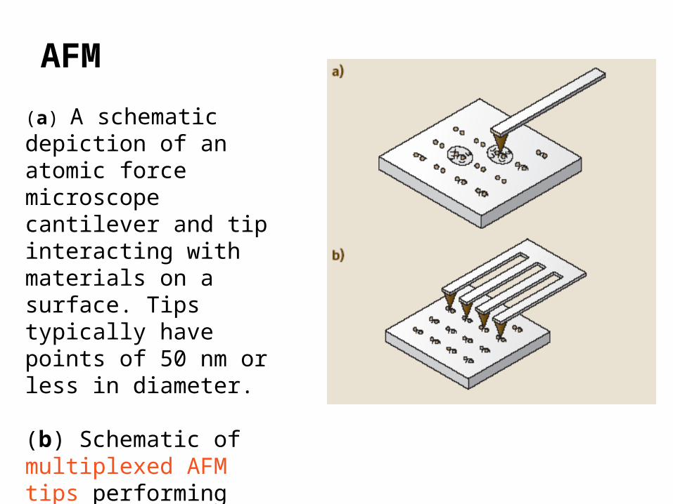
AFM
(a) A schematic depiction of an atomic force microscope cantilever and tip interacting with materials on a surface. Tips typically have points of 50 nm or less in diameter.
(b) Schematic of multiplexed AFM tips performing multiple operations in parallel.
Probes in Scanning Microscopies
― SPM images are generated through measurements of a tip-sample interaction.
― A well-characterized tip is the key element to data interpretation and is typically the limiting factor.
Probes in Scanning Microscopies
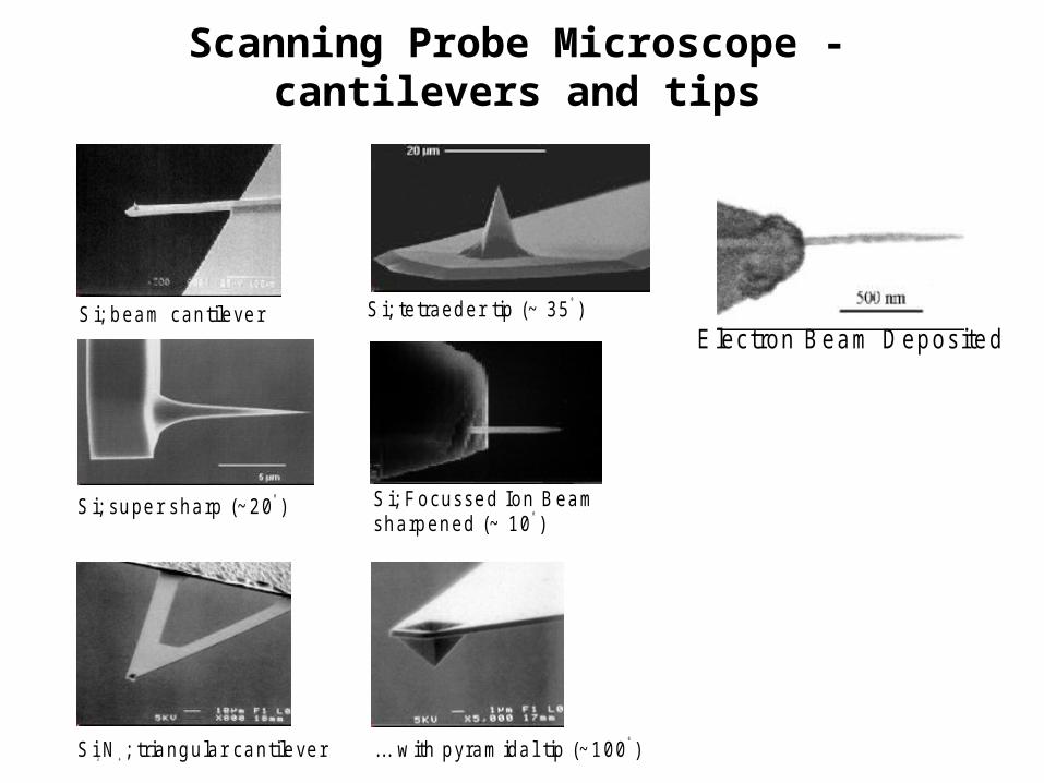
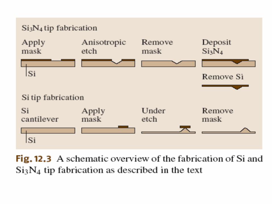
Scanning Probe Microscope - cantilevers and tips
Si; beam cantilever Si; tetraeder tip (~ 35 )0
Si; super sharp (~20 )0 Si; Focussed Ion Beam
sharpened (~ 10 )0
Si N ; triangular cantilever3 4
... w ith pyram idal tip (~100 )0
Electron Beam Deposited
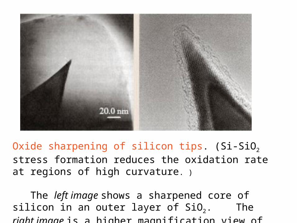
Oxide sharpening of silicon tips. (Si-SiO2 stress formation reduces the oxidation rate at regions of high curvature. )
The left image shows a sharpened core of silicon in an outer layer of SiO2. The right image is a higher magnification view of such a tip after the SiO2 is removed.
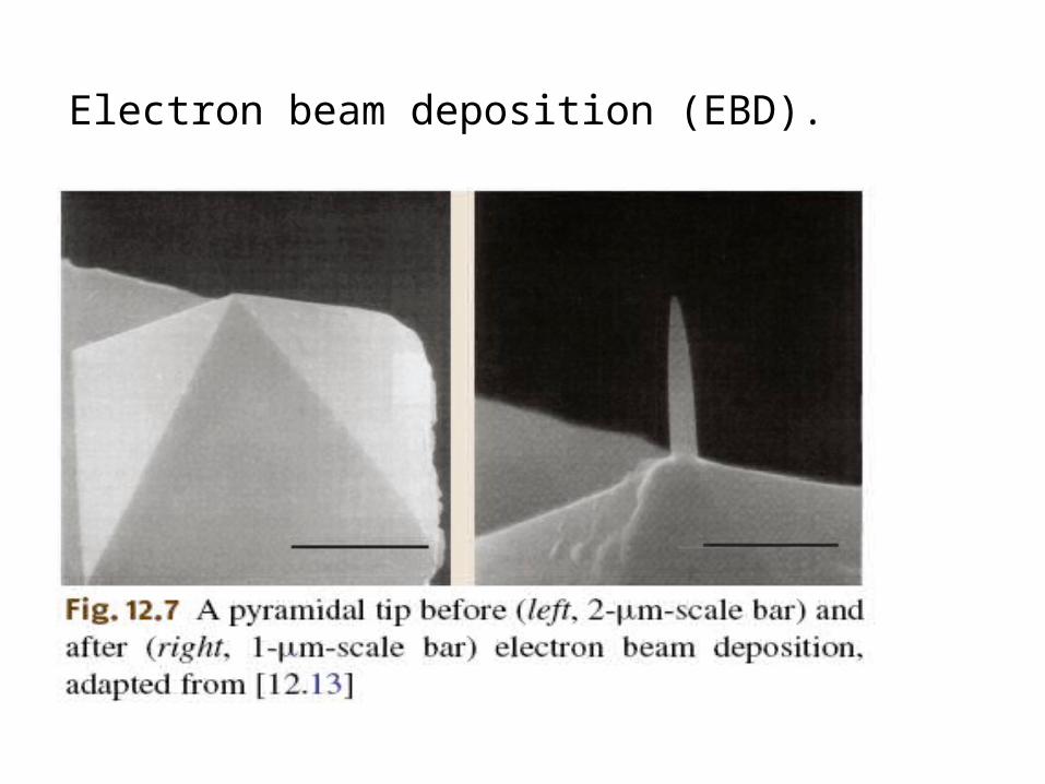
Electron beam deposition (EBD).
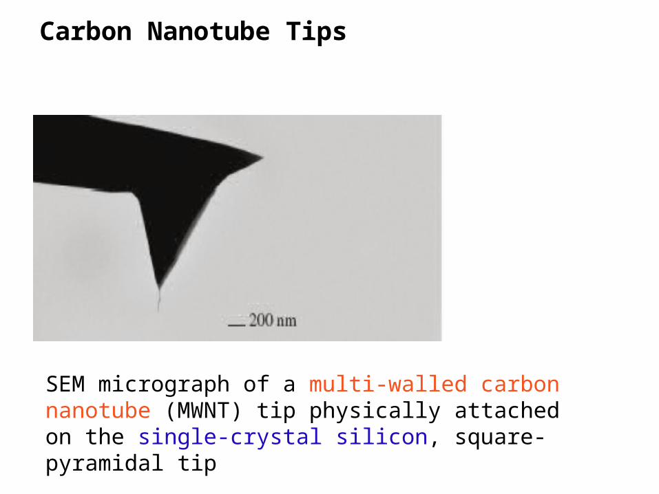
Carbon Nanotube Tips
SEM micrograph of a multi-walled carbon nanotube (MWNT) tip physically attached on the single-crystal silicon, square-pyramidal tip
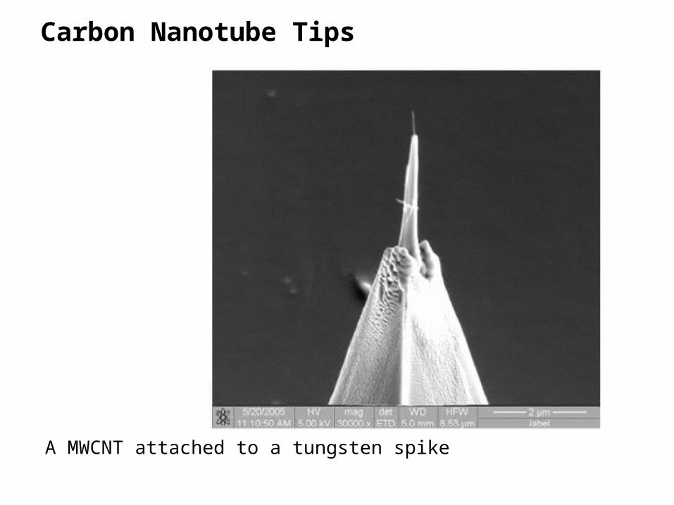
Carbon Nanotube Tips
A MWCNT attached to a tungsten spike
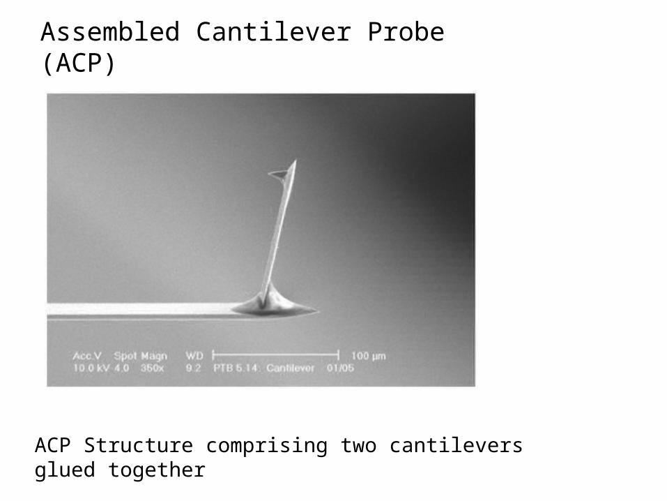
Assembled Cantilever Probe (ACP)
ACP Structure comprising two cantilevers glued together
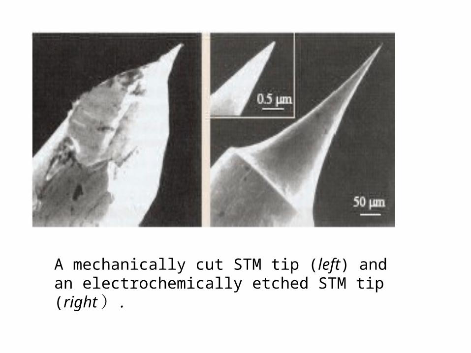
A mechanically cut STM tip (left) and an electrochemically etched STM tip (right ) .
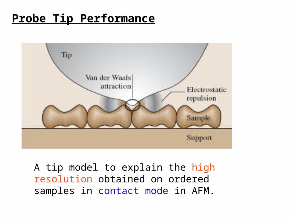
A tip model to explain the high resolution obtained on ordered samples in contact mode in AFM.
Probe Tip Performance
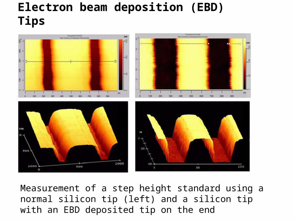
Electron beam deposition (EBD) Tips
Measurement of a step height standard using a normal silicon tip (left) and a silicon tip with an EBD deposited tip on the end
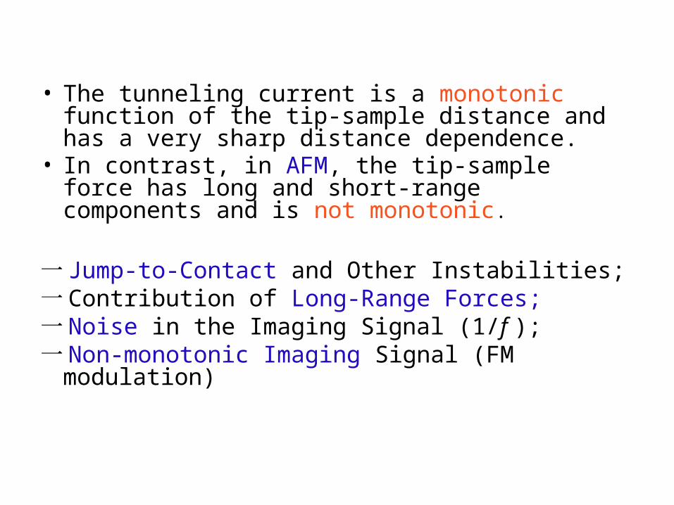
• The tunneling current is a monotonic function of the tip-sample distance and has a very sharp distance dependence.
• In contrast, in AFM, the tip-sample force has long and short-range components and is not monotonic.
一 Jump-to-Contact and Other Instabilities;一 Contribution of Long-Range Forces; 一 Noise in the Imaging Signal (1/f );一 Non-monotonic Imaging Signal (FM modulation)
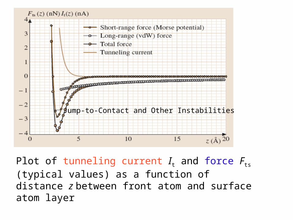
Plot of tunneling current It and force Fts (typical values) as a function of distance z between front atom and surface atom layer
一 Jump-to-Contact and Other Instabilities
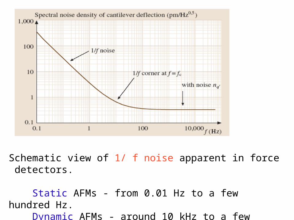
Schematic view of 1/ f noise apparent in force detectors.
Static AFMs - from 0.01 Hz to a few hundred Hz. Dynamic AFMs - around 10 kHz to a few hundred kHz.

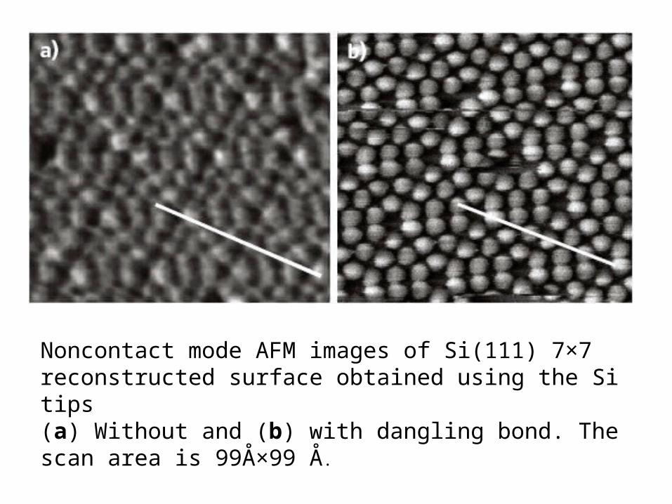
Noncontact mode AFM images of Si(111) 7×7 reconstructed surface obtained using the Si tips (a) Without and (b) with dangling bond. The scan area is 99Å×99 Å.
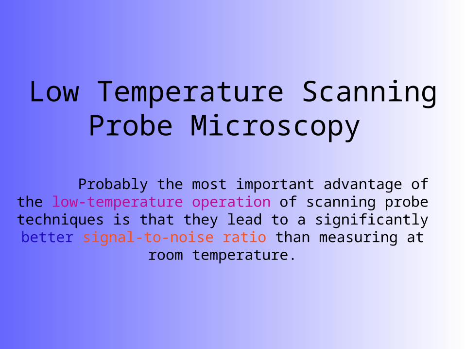
Low Temperature Scanning Probe Microscopy
Probably the most important advantage of
the low-temperature operation of scanning probetechniques is that they lead to a significantlybetter signal-to-noise ratio than measuring at
room temperature.
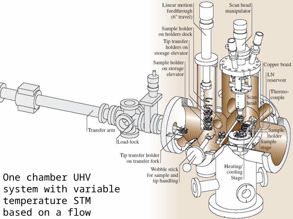
One chamber UHV system with variable temperature STM based on a flow cryostat design.
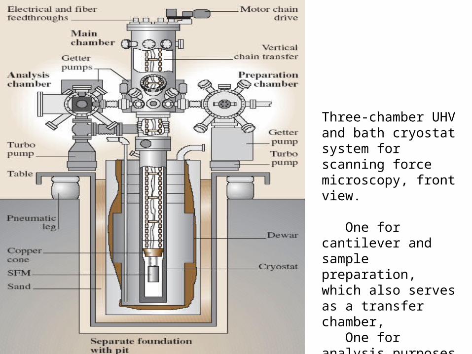
Three-chamber UHV and bath cryostat system for scanning force microscopy, front view.
One for cantilever and sample preparation,which also serves as a transfer chamber, One for analysis purposes, and A main chamber that houses the microscope.
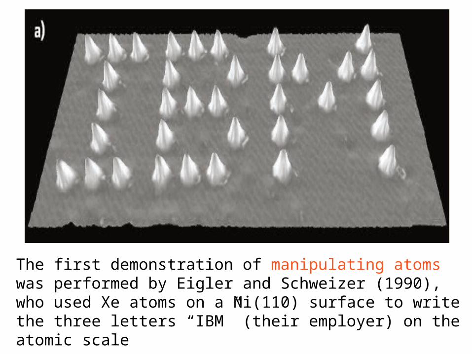
The first demonstration of manipulating atoms was performed by Eigler and Schweizer (1990), who used Xe atoms on a Ni(110) surface to write the three letters “IBM” (their employer) on the atomic scale
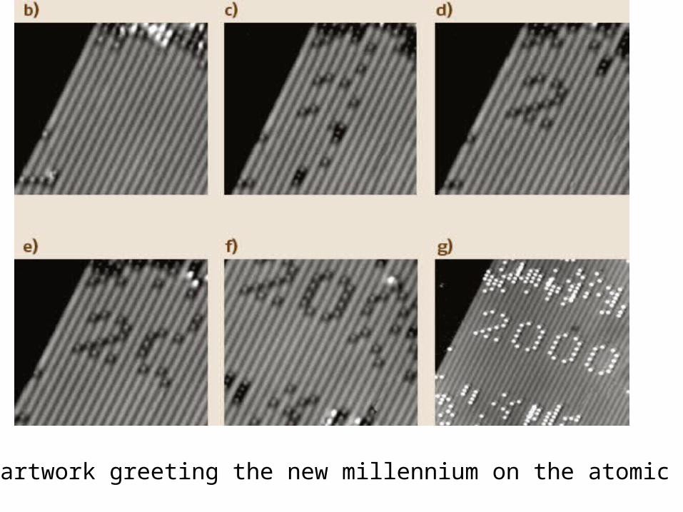
Final artwork greeting the new millennium on the atomic scale
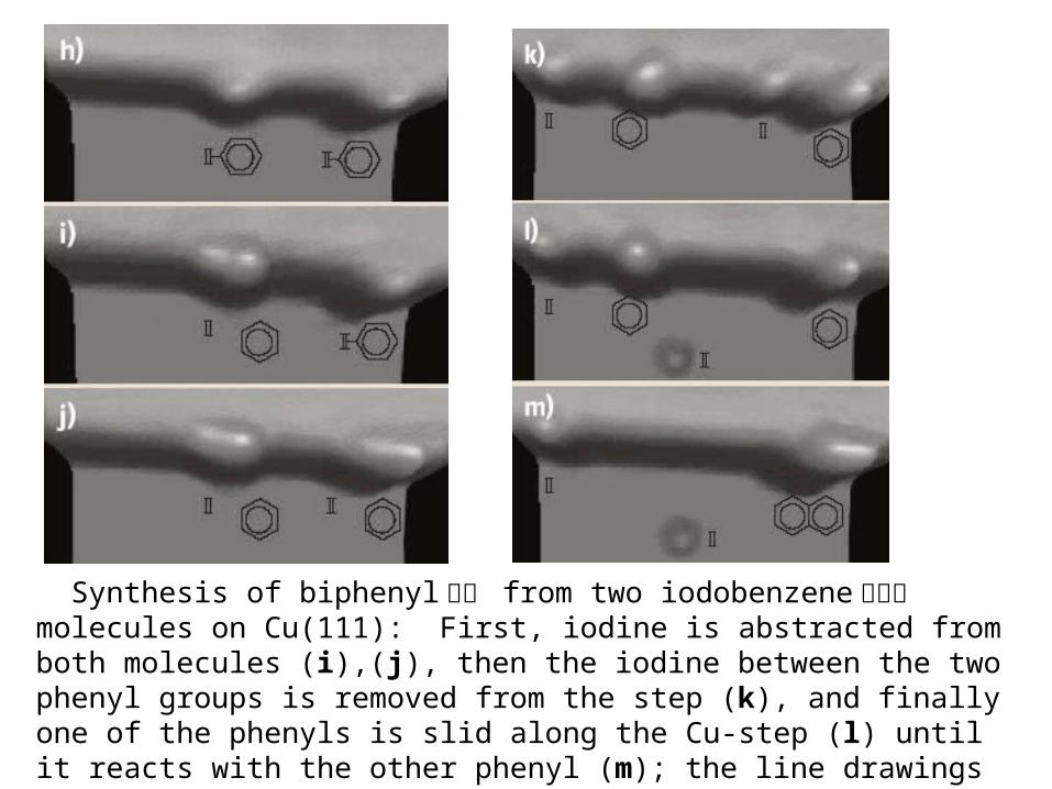
Synthesis of biphenyl 联苯 from two iodobenzene 碘代苯 molecules on Cu(111): First, iodine is abstracted from both molecules (i),(j), then the iodine between the two phenyl groups is removed from the step (k), and finally one of the phenyls is slid along the Cu-step (l) until it reacts with the other phenyl (m); the line drawings symbolize the actual status of the molecules
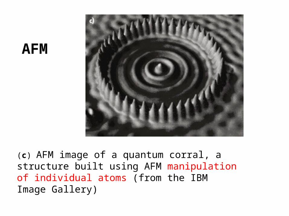
AFM
(c) AFM image of a quantum corral, a structure built using AFM manipulation of individual atoms (from the IBM Image Gallery)
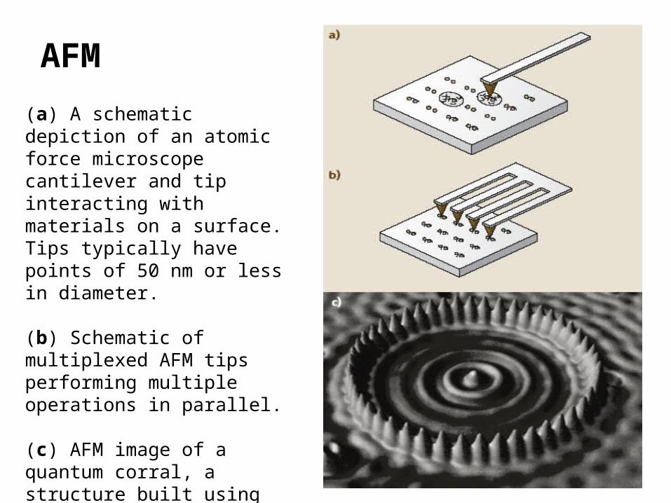
AFM
(a) A schematic depiction of an atomic force microscope cantilever and tip interacting with materials on a surface. Tips typically have points of 50 nm or less in diameter.
(b) Schematic of multiplexed AFM tips performing multiple operations in parallel.
(c) AFM image of a quantum corral, a structure built using AFM manipulation of individual atoms (from the IBM Image Gallery)