schematic checklist usb2514b qfn b - microchip...
TRANSCRIPT
REV
CHANGE DESCRIPTION
NAME
DATE
A
Release
3-6-17
Any assistance, services, comments, information, or suggestions provided by Microchip (including without limitation any comments to the effect that the Company’s product designs do not require any changes) (collectively, “Microchip Feedback”) are provided solely for the purpose of assisting the Company in the Company’s attempt to optimize compatibility of the Company’s product designs with certain Microchip products. Microchip does not promise that such compatibility optimization will actually be achieved. Circuit diagrams utilizing Microchip products are included as a means of illustrating typical applications; consequently, complete information sufficient for construction purposes is not necessarily given. Although the information has been checked and is believed to be accurate, no responsibility is assumed for inaccuracies. Microchip reserves the right to make changes to specifications and product descriptions at any time without notice.
DOCUMENT DESCRIPTION
Schematic Checklist for the USB2514B, 36-pin QFN Package
Microchip 80 Arkay Drive, Suite 100 Hauppauge, New York 11788
Document Number Revision
SC571231 A
USB2514B Schematic Checklist
Page 2 of 24
Revision A
Schematic Checklist for USB2514B
Information Particular for the 36-pin QFN Package
USB Upstream Interface Port 0: 1. USBDP_UP (pin 31), this pin is the USB Upstream channel positive data pin. This pin
should be connected directly to pin 3 (D+) on a standard 4-pin, upstream USB connector (Type “B”).
2. USBDM_UP (pin 30), this pin is the USB Upstream channel negative data pin. This pin
should be connected directly to pin 2 (D-) on a standard 4-pin, upstream USB connector (Type “B”).
3. Typical applications will connect pin 4 (Ground) on a standard 4-pin, upstream USB
connector (Type “B”) directly to digital ground.
4. Pin 1 (VBUS) on the Upstream USB connector can be configured in one of two ways. In Bus-Powered Mode, pin 1 draws +5V power (VBUS) from the Host side and typically powers a +3.3V regulator to power the system. In Self-Powered Mode, pin 1 (VBUS) simply acts as a sensory circuit in order to alert the Hub that a Host is connected.
5. The two metal shield connections on the USB connector should be connected directly to
a suitable chassis ground plane.

USB2514B Schematic Checklist
Page 3 of 24
Revision A
VBUS_DET Configurations: Possible VBUS_DET pin (pin 27) connections are dictated by the hardware configuration of the USB link. Possible designs are “Self-Powered Mode”, “Self-Powered Permanently Attached Mode” and “Bus-Powered Mode”. These three possible configurations are depicted below.
Self-Powered Mode:
USB2514B
+3.3V Ext Power Supply
USB USB Host
USB
VBUS_DET +5V+3.3VVDD33
1. In this application, the VBUS_DET pin (pin 27) is driven by a voltage divider circuit that drops the +5V VBUS voltage to +3.3V.
2. For the voltage divider, a series 100K ohm resistor with a 100K ohm resistor to digital
ground is recommended.
3. A 1.0 uF capacitor is also recommended on pin 1 (VBUS) of the USB connector.

USB2514B Schematic Checklist
Page 4 of 24
Revision A
Self-Powered Permanently Attached Mode:
1. In this application, the VBUS_DET pin (pin 27) is driven by the same power rail that powers both the USB2514B and the USB Host.
2. A series resistor (820 ohms to 10K ohms) may be used on the VBUS_DET pin in order to
improve susceptibility characteristics.
USB2514B Schematic Checklist
Page 5 of 24
Revision A
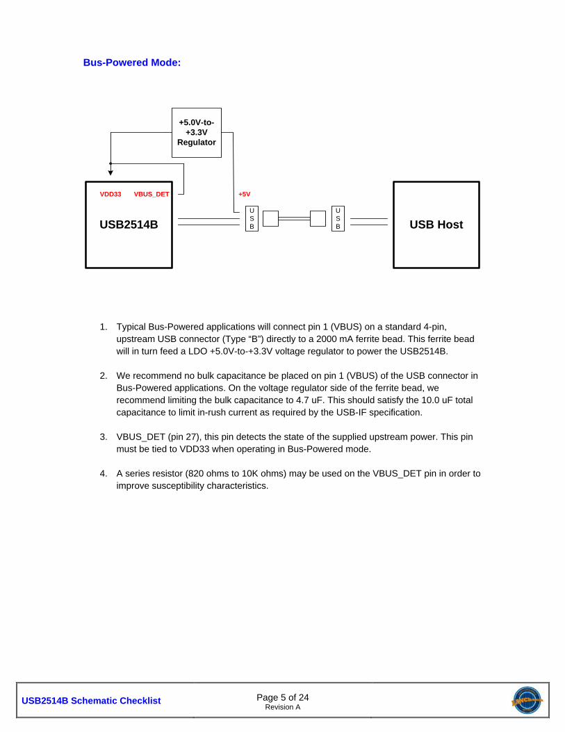
Bus-Powered Mode:
USB2514B
+5.0V-to-+3.3V
Regulator
USB USB Host
USB
VBUS_DET +5VVDD33
1. Typical Bus-Powered applications will connect pin 1 (VBUS) on a standard 4-pin, upstream USB connector (Type “B”) directly to a 2000 mA ferrite bead. This ferrite bead will in turn feed a LDO +5.0V-to-+3.3V voltage regulator to power the USB2514B.
2. We recommend no bulk capacitance be placed on pin 1 (VBUS) of the USB connector in
Bus-Powered applications. On the voltage regulator side of the ferrite bead, we recommend limiting the bulk capacitance to 4.7 uF. This should satisfy the 10.0 uF total capacitance to limit in-rush current as required by the USB-IF specification.
3. VBUS_DET (pin 27), this pin detects the state of the supplied upstream power. This pin
must be tied to VDD33 when operating in Bus-Powered mode.
4. A series resistor (820 ohms to 10K ohms) may be used on the VBUS_DET pin in order to improve susceptibility characteristics.

USB2514B Schematic Checklist
Page 6 of 24
Revision A
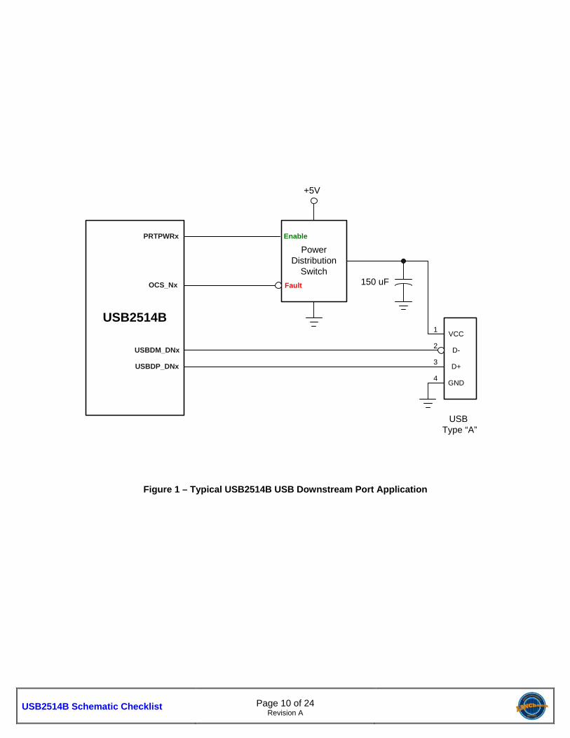
USB Downstream Interface Port 1: 1. USBDP_DN1 (pin 2), this pin is the USB Downstream Port 1 channel positive data pin.
This pin should be connected directly to pin 3 (D+) on a standard 4-pin, downstream USB connector (Type “A”).
2. USBDM_DN1 (pin 1), this pin is the USB Downstream Port 2 channel negative data pin.
This pin should be connected directly to pin 2 (D-) on a standard 4-pin, downstream USB connector (Type “A”).
3. Typical applications will connect pin 1 (VCC) on a standard 4-pin, downstream USB
connector (Type “A”) directly to output of a power distribution switch. This will supply power to the downstream device. Other power distribution schemes are possible; see the latest copy of the USB2514B data sheet for more details on using a poly fuse for USB power distribution.
4. In addition, Microchip recommends the addition of a 150 uF capacitor to be placed on pin
1 (VCC) on a standard 4-pin, downstream USB connector (Type “A”). This will ensure that the required USB Voltage Drop and Voltage Droop specifications are met for the downstream device.
5. Typical applications will connect pin 4 (Ground) on a standard 4-pin, downstream USB
connector (Type “A”) directly to digital ground.
6. The two metal shield connections on the USB connector should be connected directly to a suitable chassis ground plane.
7. PRTPWR1 (pin 12), this output pin of the USB2514B is connected to the input enable pin
on the USB Port Power Controller for Port 1. PRTPWR1 is an active-high enable signal. When enabled, the USB Port Power Controller will supply +5V VBUS power to pin 1 on the downstream USB connector. For this reason, care must be taken when selecting a power distribution switch for the USB2514B. Power distribution switches are available with active high enables or active low enables. Active low enable parts will not work with the USB2514B. The power distribution switch must have an active high enable input and an over-current fault indication active low output.
8. OCS_N1 (pin 13), this input pin samples the Flag (or Over Current Sense) output signal from the power distribution switch for Port 1. An over-current condition is indicated when the signal is low.

USB2514B Schematic Checklist
Page 7 of 24
Revision A
USB Downstream Interface Port 2: 1. USBDP_DN2 (pin 4), this pin is the USB Downstream Port 2 channel positive data pin.
This pin should be connected directly to pin 3 (D+) on a standard 4-pin, downstream USB connector (Type “A”).
2. USBDM_DN2 (pin 3), this pin is the USB Downstream Port 3 channel negative data pin.
This pin should be connected directly to pin 2 (D-) on a standard 4-pin, downstream USB connector (Type “A”).
3. Typical applications will connect pin 1 (VCC) on a standard 4-pin, downstream USB
connector (Type “A”) directly to output of a power distribution switch. This will supply power to the downstream device. Other power distribution schemes are possible; see the latest copy of the USB2514B data sheet for more details on using a poly fuse for USB power distribution.
4. In addition, Microchip recommends the addition of a 150 uF capacitor to be placed on pin
1 (VCC) on a standard 4-pin, downstream USB connector (Type “A”). This will ensure that the required USB Voltage Drop and Voltage Droop specifications are met for the downstream device.
5. Typical applications will connect pin 4 (Ground) on a standard 4-pin, downstream USB
connector (Type “A”) directly to digital ground.
6. The two metal shield connections on the USB connector should be connected directly to a suitable chassis ground plane.
7. PRTPWR2 (pin 16), this output pin of the USB2514B is connected to the input enable pin on the USB Port Power Controller for Port 2. PRTPWR2 is an active-high enable signal. When enabled, the USB Port Power Controller will supply +5V VBUS power to pin 1 on the downstream USB connector. For this reason, care must be taken when selecting a power distribution switch for the USB2514B. Power distribution switches are available with active high enables or active low enables. Active low enable parts will not work with the USB2514B. The power distribution switch must have an active high enable input and an over-current fault indication active low output.
8. OCS_N2 (pin 17), this input pin samples the Flag (or Over Current Sense) output signal from the power distribution switch for Port 2. An over-current condition is indicated when the signal is low.

USB2514B Schematic Checklist
Page 8 of 24
Revision A
USB Downstream Interface Port 3: 1. USBDP_DN3 (pin 7), this pin is the USB Downstream Port 3 channel positive data pin.
This pin should be connected directly to pin 3 (D+) on a standard 4-pin, downstream USB connector (Type “A”).
2. USBDM_DN3 (pin 6), this pin is the USB Downstream Port 3 channel negative data pin.
This pin should be connected directly to pin 2 (D-) on a standard 4-pin, downstream USB connector (Type “A”).
3. Typical applications will connect pin 1 (VCC) on a standard 4-pin, downstream USB
connector (Type “A”) directly to output of a power distribution switch. This will supply power to the downstream device. Other power distribution schemes are possible; see the latest copy of the USB2514B data sheet for more details on using a poly fuse for USB power distribution.
4. In addition, Microchip recommends the addition of a 150 uF capacitor to be placed on pin
1 (VCC) on a standard 4-pin, downstream USB connector (Type “A”). This will ensure that the required USB Voltage Drop and Voltage Droop specifications are met for the downstream device.
5. Typical applications will connect pin 4 (Ground) on a standard 4-pin, downstream USB
connector (Type “A”) directly to digital ground.
6. The two metal shield connections on the USB connector should be connected directly to a suitable chassis ground plane.
7. PRTPWR3 (pin 18), this output pin of the USB2514B is connected to the input enable pin
on the USB Port Power Controller for Port 3. PRTPWR3 is an active-high enable signal. When enabled, the USB Port Power Controller will supply +5V VBUS power to pin 1 on the downstream USB connector. For this reason, care must be taken when selecting a power distribution switch for the USB2514B. Power distribution switches are available with active high enables or active low enables. Active low enable parts will not work with the USB2514B. The power distribution switch must have an active high enable input and an over-current fault indication active low output.
8. OCS_N3 (pin 19), this input pin samples the Flag (or Over Current Sense) output signal from the power distribution switch for Port 3. An over-current condition is indicated when the signal is low.
USB2514B Schematic Checklist
Page 9 of 24
Revision A
USB Downstream Interface Port 4: 1. USBDP_DN4 (pin 9), this pin is the USB Downstream Port 4 channel positive data pin.
This pin should be connected directly to pin 3 (D+) on a standard 4-pin, downstream USB connector (Type “A”).
2. USBDM_DN4 (pin 8), this pin is the USB Downstream Port 4 channel negative data pin.
This pin should be connected directly to pin 2 (D-) on a standard 4-pin, downstream USB connector (Type “A”).
3. Typical applications will connect pin 1 (VCC) on a standard 4-pin, downstream USB
connector (Type “A”) directly to output of a power distribution switch. This will supply power to the downstream device. Other power distribution schemes are possible; see the latest copy of the USB2514B data sheet for more details on using a poly fuse for USB power distribution.
4. In addition, Microchip recommends the addition of a 150 uF capacitor to be placed on pin
1 (VCC) on a standard 4-pin, downstream USB connector (Type “A”). This will ensure that the required USB Voltage Drop and Voltage Droop specifications are met for the downstream device.
5. Typical applications will connect pin 4 (Ground) on a standard 4-pin, downstream USB
connector (Type “A”) directly to digital ground.
6. The two metal shield connections on the USB connector should be connected directly to a suitable chassis ground plane.
7. PRTPWR4 (pin 20), this output pin of the USB2514B is connected to the input enable pin
on the USB Port Power Controller for Port 4. PRTPWR4 is an active-high enable signal. When enabled, the USB Port Power Controller will supply +5V VBUS power to pin 1 on the downstream USB connector. For this reason, care must be taken when selecting a power distribution switch for the USB2514B. Power distribution switches are available with active high enables or active low enables. Active low enable parts will not work with the USB2514B. The power distribution switch must have an active high enable input and an over-current fault indication active low output.
8. OCS_N4 (pin 21), this input pin samples the Flag (or Over Current Sense) output signal from the power distribution switch for Port 1. An over-current condition is indicated when the signal is low.
USB2514B Schematic Checklist
Page 10 of 24
Revision A
USB2514B
PowerDistribution
Switch
+5V
Fault
EnablePRTPWRx
USBDM_DNx
USBDP_DNx
1
2
3
4
VCC
D-
D+
GND
USBType “A”
150 uFOCS_Nx
Figure 1 – Typical USB2514B USB Downstream Port Application

USB2514B Schematic Checklist
Page 11 of 24
Revision A
+3.3V Power Supply Connections:
1. The digital supply (VDD33) pins on the USB2514B QFN are 15 & 23. They require a connection to +3.3V.
2. Each VDD33 power pin should have one .01 F (or smaller) capacitor to decouple the
USB2514B. The capacitor size should be SMD_0603 or smaller.
3. The analog supply (VDDA33) pins on the USB2514B QFN are 5, 10, 29 & 36. They require a connection to +3.3V through a ferrite bead. Be sure to place bulk capacitance on each side of the ferrite bead.
4. Each VDDA33 pin should have one .01 F (or smaller) capacitor to decouple the
USB2514B. The capacitor size should be SMD_0603 or smaller.
VD
D33
VD
DA
33
Figure 2 - +3.3V Power Supply Connections
USB2514B Schematic Checklist
Page 12 of 24
Revision A
CRFILT:
1. CRFILT (pin 14), this pin provides bypassing for the +1.2V core regulator. The pin requires a 0.01 F decoupling/bypass capacitor. The capacitor should be located as close as possible to pin 14 without using vias. In addition, pin 14 requires a bulk capacitor placed as close as possible to pin
14. The bulk capacitor must have a value of at least 0.1 F, and have an ESR (equivalent series
resistance) of no more than 2.0 . Microchip recommends a very low ESR ceramic capacitor for design stability. Other values, tolerances & characteristics are not recommended.
Caution: Even though both are +1.2V levels, Do Not Connect CRFILT to PLLFILT. Caution: This +1.2V supply is for internal logic only and USB2514B use only. Do Not power
other external circuits or devices with this supply.
PLLFILT:
1. PLLFILT (pin 34), this pin provides bypassing for the second +1.2V regulator. The pin requires a
0.01 F decoupling/bypass capacitor. The capacitor should be located as close as possible to pin 34 without using vias. In addition, pin 34 requires a bulk capacitor placed as close as possible to
pin 34. The bulk capacitor must have a value of at least 0.1 F, and have an ESR (equivalent
series resistance) of no more than 2.0 . Microchip recommends a very low ESR ceramic capacitor for design stability. Other values, tolerances & characteristics are not recommended.
Caution: Even though both are +1.2V levels, Do Not Connect PLLFILT to CRFILT. Caution: This +1.2V supply is for internal logic only and USB2514B use only. Do Not power
other external circuits or devices with this supply.

USB2514B Schematic Checklist
Page 13 of 24
Revision A
Figure 3 - USB2514B +1.2V Power Connections
Ground Connections:
1. All grounds, the digital ground pins (GND), the core ground pins (GND_CORE) and the analog ground pins (VSS_A) on the USB2514B QFN, are all connected internally to the exposed die paddle ground (VSS). The EDP Ground pad on the underside of the USB2514B must be connected directly to a solid, contiguous digital ground plane.
2. On the PCB, we recommend one Digital Ground. We do not recommend running
separate ground planes for any of our LAN products.

USB2514B Schematic Checklist
Page 14 of 24
Revision A
Crystal Connections:
1. A 24.000 MHz crystal must be used with the USB2514B QFN. For exact specifications and tolerances refer to the latest revision USB2514B data sheet.
2. XTALIN (pin 33) on the USB2514B QFN is the clock circuit input. This pin requires a 15 –
33 F capacitor to digital ground. One side of the crystal connects to this pin.
3. XTALOUT (pin 32) on the USB2514B QFN is the clock circuit output. This pin requires a matching 15 – 33 F capacitor to ground and the other side of the crystal.
4. Since every system design is unique, the capacitor values are system dependant. The
PCB design, the crystal selected, the layout and the type of caps selected all contribute to the characteristics of this circuit. Once the board is complete and operational, it is up to the system engineer to analyze this circuit in a lab environment. The system engineer should verify the frequency, the stability and the voltage level of the circuit to guarantee that the circuit meets all design criteria as put forth in the data sheet.
5. For proper operation, the additional external 1.0M resistor across the crystal is no longer required. The necessary resistance has been designed-in internally on the USB2514B SQFN.
EEPROM Interface:
1. Enhanced OEM configuration options can be loaded into the USB2514B via the use of an optional external serial I2C EEPROM. Otherwise, the USB2514B will use it’s default register values.
2. SCL (pin 24) on the USB2514B QFN connects to the external I2C EEPROM’s serial clock pin.
3. SDA (pin 22) on the USB2514B QFN connects to the external I2C EEPROM’s serial data pin.
4. Be sure to select a 2-wire style 2K I2C EEPROM that is organized for 256 x 8-bit
operation.
5. The hub will read the external EEPROM for configuration data and then attach to the upstream USB host. The hub does not have the capacity to write to the external EEPROM.
USB2514B Schematic Checklist
Page 15 of 24
Revision A
SMBus Interface:
1. Enhanced OEM configuration options can also be loaded into the USB2514B via the USB2514B being configured as an SMBus Slave. The Microchip hub can then be configured by an external processor (Master) via the SMBus interface. This strategy is also optional and otherwise, the USB2514B will use it’s default register values.
2. SMBCLK (pin 24) on the USB2514B QFN connects to the external SMBus Master’s serial clock pin.
3. SMBDATA (pin 22) on the USB2514B QFN connects to the external SMBus Master’s serial data pin.
4. The hub waits indefinitely for the SMBus code load to complete and only appears as a newly connected device on USB after the code load is complete. The hub’s SMBus acts as a slave-only SMBus device.
5. The 7-bit slave address is 0101100b. The hub will not respond to the general call address of 0000000b.
RBIAS Resistor:
1. RBIAS (pin 35) on the USB2514B QFN should connect to digital ground through a 12.0K resistor with a tolerance of 1.0%. This pin is used to set-up critical bias currents for the embedded USB Physical device.
Required External Pull-ups/Pull-downs:
1. SMBCLK (pin 24) requires a 10.0K ohm pull-up resistor (VDD33) in order to guarantee proper operation in SMBus mode.
2. SMBDATA (pin 22) requires a 10.0K ohm pull-up resistor (VDD33) in order to guarantee proper operation in SMBus mode.
USB2514B Schematic Checklist
Page 16 of 24
Revision A
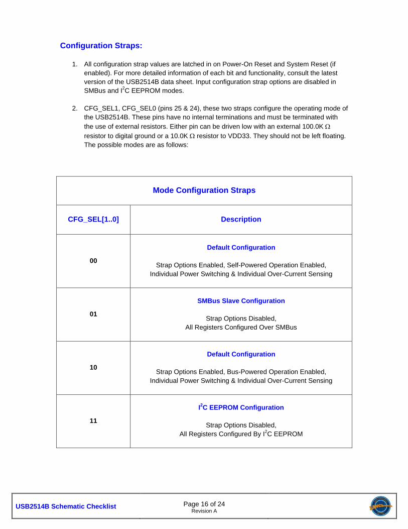
Configuration Straps:
1. All configuration strap values are latched in on Power-On Reset and System Reset (if enabled). For more detailed information of each bit and functionality, consult the latest version of the USB2514B data sheet. Input configuration strap options are disabled in SMBus and I2C EEPROM modes.
2. CFG_SEL1, CFG_SEL0 (pins 25 & 24), these two straps configure the operating mode of
the USB2514B. These pins have no internal terminations and must be terminated with
the use of external resistors. Either pin can be driven low with an external 100.0K
resistor to digital ground or a 10.0K resistor to VDD33. They should not be left floating. The possible modes are as follows:
Mode Configuration Straps
CFG_SEL[1..0]
Description
00
Default Configuration
Strap Options Enabled, Self-Powered Operation Enabled,
Individual Power Switching & Individual Over-Current Sensing
01
SMBus Slave Configuration
Strap Options Disabled,
All Registers Configured Over SMBus
10
Default Configuration
Strap Options Enabled, Bus-Powered Operation Enabled,
Individual Power Switching & Individual Over-Current Sensing
11
I2C EEPROM Configuration
Strap Options Disabled,
All Registers Configured By I2C EEPROM

USB2514B Schematic Checklist
Page 17 of 24
Revision A
3. NON_REM1, NON_REM0 (pins 22 & 28), these two straps configure the presence of permanently attached (non-removable) devices on the downstream ports of the USB2514B. These pins have no internal terminations and must be terminated with the use of external resistors. Either pin can be driven low with an external 100.0K resistor
to digital ground or a 10.0K resistor to VDD33. They should not be left floating. The possible modes are as follows:
NON_REMx Mode Configuration Straps
NON_REM[1..0]
Description
00
All Downstream Ports Are Removable
01
Port 1 Is Non-Removable (Permanently Attached)
10
Port 1 & Port 2 Are Non-Removable (Permanently Attached)
11
Port 1, Port 2 & Port 3 Are Non-Removable (Permanently Attached)
4. Design Note: For Removable / Non-Removable cases, there are three configurations:
A. If a port has a USB connector exposed to the consumer, it is Removable.
B. If a port does not have a USB connector and never has a device connected, it should be disabled.
C. If a port does not have a USB connector but usually has a device connected
(Permanently Attached), it should be configured as Non-Removable. It is OK for this device to periodically reset and detach.

USB2514B Schematic Checklist
Page 18 of 24
Revision A
5. Design Note: Describing the Downstream Ports accurately in a USB design as far as Removable / Non-Removable is concerned is important with regards to USB Compliance testing implications. When the USB compliance software runs, it will check for various port functionality (like the ability to wake the device up upon device attach, ability of not to wake up when this function is disabled, etc, etc). This is done by instructing the person who conducts the test to plug-unplug a regular USB mouse to ports under test, multiple times. If the design has embedded devices permanently attached to some ports and they are not declared as "non-removable", the software will assume that these ports are "user accessible", and will wait for operator to plug-unplug the test mouse into it, which obviously will be impossible. So, the test will time-out and fail, failing the entire certification. If your Removable ports are described as Non-Removable at the time of testing, the software will flag the discrepancy between test declarations and descriptors, and the certification will also fail. It is recommended that the design engineer accurately describe the system (Removable / Non-Removable) if USB compliance is important. Some designs may require re-ordering of the USB ports in the schematic to accomplish this.
6. LOCAL_PWR (pin 28), this input configuration strap is only operational when Dynamic
Power Switching is Enabled. A USB register write is required to enable Dynamic Power Switching in the hub. See the data sheet for more details. The LOCAL_PWR pin, when enabled, configures the hub for either Bus-Powered operation or Self-Powered operation. The settings are as follows:
0 = Bus-Powered (Hub gets all it’s from the Upstream USB VBUS) 1 = Self-Powered
See the latest version of the USB2514B data sheet for complete details.
7. PRT_DIS_P1 (pin 2) and PRT_DIS_M1 (pin 1), if input configuration strap options are
enabled, these two pins enable / disable the Down Stream Port 1 on the Hub. The two terminations should be referenced to VDD33. Both pins must be terminated in the same manner; the settings are as follows:
0 = Port 1 Enabled (No External Terminations Added) 1 = Port 1 Disabled (10.0K Added to Both Pins)
See the latest version of the USB2514B data sheet for complete details.
8. PRT_DIS_P2 (pin 4) and PRT_DIS_M2 (pin 3), if input configuration strap options are enabled, these two pins enable / disable the Down Stream Port 2 on the Hub. The two terminations should be referenced to VDD33. Both pins must be terminated in the same manner; the settings are as follows:
0 = Port 1 Enabled (No External Terminations Added)
1 = Port 1 Disabled (10.0K Added to Both Pins)
See the latest version of the USB2514B data sheet for complete details.

USB2514B Schematic Checklist
Page 19 of 24
Revision A
9. PRT_DIS_P3 (pin 7) and PRT_DIS_M3 (pin 6), if input configuration strap options are
enabled, these two pins enable / disable the Down Stream Port 3 on the Hub. The two terminations should be referenced to VDD33. Both pins must be terminated in the same manner; the settings are as follows:
0 = Port 1 Enabled (No External Terminations Added)
1 = Port 1 Disabled (10.0K Added to Both Pins)
See the latest version of the USB2514B data sheet for complete details.
10. PRT_DIS_P4 (pin 9) and PRT_DIS_M4 (pin 8), if input configuration strap options are enabled, these two pins enable / disable the Down Stream Port 4 on the Hub. The two terminations should be referenced to VDD33. Both pins must be terminated in the same manner; the settings are as follows:
0 = Port 1 Enabled (No External Terminations Added) 1 = Port 1 Disabled (10.0K Added to Both Pins)
See the latest version of the USB2514B data sheet for complete details.
11. BC_EN1 (pin 12), if input configuration strap options are enabled, this pin enables /
disables the battery charging protocol on Downstream Port 1. When supporting the battery charging protocol, the hub also supports external port power controllers. The battery charging protocol enables a device to draw the currents per the USB battery charging specification. The termination should be referenced to VDD33. The settings are as follows:
0 = Battery Charging Feature Is Not Supported Port 1 (internal PD) 1 = Battery Charging Feature Is Supported Port 1 (10.0K Added)
See the latest version of the USB2514B data sheet for complete details.
12. BC_EN2 (pin 16), if input configuration strap options are enabled, this pin enables /
disables the battery charging protocol on Downstream Port 2. When supporting the battery charging protocol, the hub also supports external port power controllers. The battery charging protocol enables a device to draw the currents per the USB battery charging specification. The termination should be referenced to VDD33. The settings are as follows:
0 = Battery Charging Feature Is Not Supported Port 2 (internal PD) 1 = Battery Charging Feature Is Supported Port 2 (10.0K Added)
See the latest version of the USB2514B data sheet for complete details.

USB2514B Schematic Checklist
Page 20 of 24
Revision A
13. BC_EN3 (pin 18), if input configuration strap options are enabled, this pin enables / disables the battery charging protocol on Downstream Port 3. When supporting the battery charging protocol, the hub also supports external port power controllers. The battery charging protocol enables a device to draw the currents per the USB battery charging specification. The termination should be referenced to VDD33. The settings are as follows:
0 = Battery Charging Feature Is Not Supported Port 3 (internal PD) 1 = Battery Charging Feature Is Supported Port 3 (10.0K Added)
See the latest version of the USB2514B data sheet for complete details.
14. BC_EN4 (pin 20), if input configuration strap options are enabled, this pin enables /
disables the battery charging protocol on Downstream Port 4. When supporting the battery charging protocol, the hub also supports external port power controllers. The battery charging protocol enables a device to draw the currents per the USB battery charging specification. The termination should be referenced to VDD33. The settings are as follows:
0 = Battery Charging Feature Is Not Supported Port 4 (internal PD)
1 = Battery Charging Feature Is Supported Port 4 (10.0K Added)
See the latest version of the USB2514B data sheet for complete details.
15. Design Note: The USB2514B supports the USB Battery Charging Specification Revision 1.1 for Charging Downstream Ports (CDP). When configured for Battery Charging Mode, the PRTPWR[4..1] pin behavior is different than Non-Battery Charging mode operation. Also, when configured for CDP, the +5V VBUS supply and the Port Power Controller / Over-Current Protection device(s) must be able to support 1.5 amps of power; so device selection is important. When not supporting Battery Charging, the +5V VBUS rail and PPC / OCP devices need only to be rated for 0.8 amps of power. See the latest USB2514B data sheet for more details on this subject.
USB2514B Schematic Checklist
Page 21 of 24
Revision A
Miscellaneous: 1. RESET_N (pin 26), is an active-low reset input. This signal resets all logic and registers
within the USB2514B. A hardware reset (RESET_N assertion) is required following power-up. Please refer to the latest copy of the USB2514B data sheet for reset timing requirements. Microchip does not recommend the use of an RC circuit for this required pin reset. A reset generator / voltage monitor is one option to provide a proper reset. Better yet, for increased design flexibility, a controllable reset (GPIO, dedicated reset output) should be considered. In this case, Microchip recommends a push-pull type output (not an open-drain type) for the monotonic reset to ensure a sharp rise time transition from low-to-high.
2. HS_IND (pin 25), this pin indicates the Upstream Port speed connection. See the latest version of the USB2514B data sheet for complete details.
0 = Hub Is Connected At Full Speed (12 Mbit/s) 1 = Hub Is Connected At High Speed (480 Mbit/s)
3. SUSP_IND (pin 28), this pin indicates the USB State of the USB2514B. See the latest version of the USB2514B data sheet for complete details.
0 = Hub Is Unconfigured Or Configured And In USB Suspend Mode 1 = Hub Is Configured And Is Active (Not In Suspend)
4. TEST (pin 11), this pin must be tied directly to digital ground in order to ensure proper operation.
5. Incorporate a large SMD resistor (SMD_1210) to connect the USB chassis ground to the
digital ground. This will allow some flexibility at EMI testing for different grounding options. Leave the resistor out, the two grounds are separate. Short them together with a zero ohm resistor. Short them together with a cap or a ferrite bead for best performance.
6. Be sure to incorporate enough bulk capacitors (4.7 - 22F caps) for each power plane.

USB2514B Schematic Checklist
Page 22 of 24
Revision A
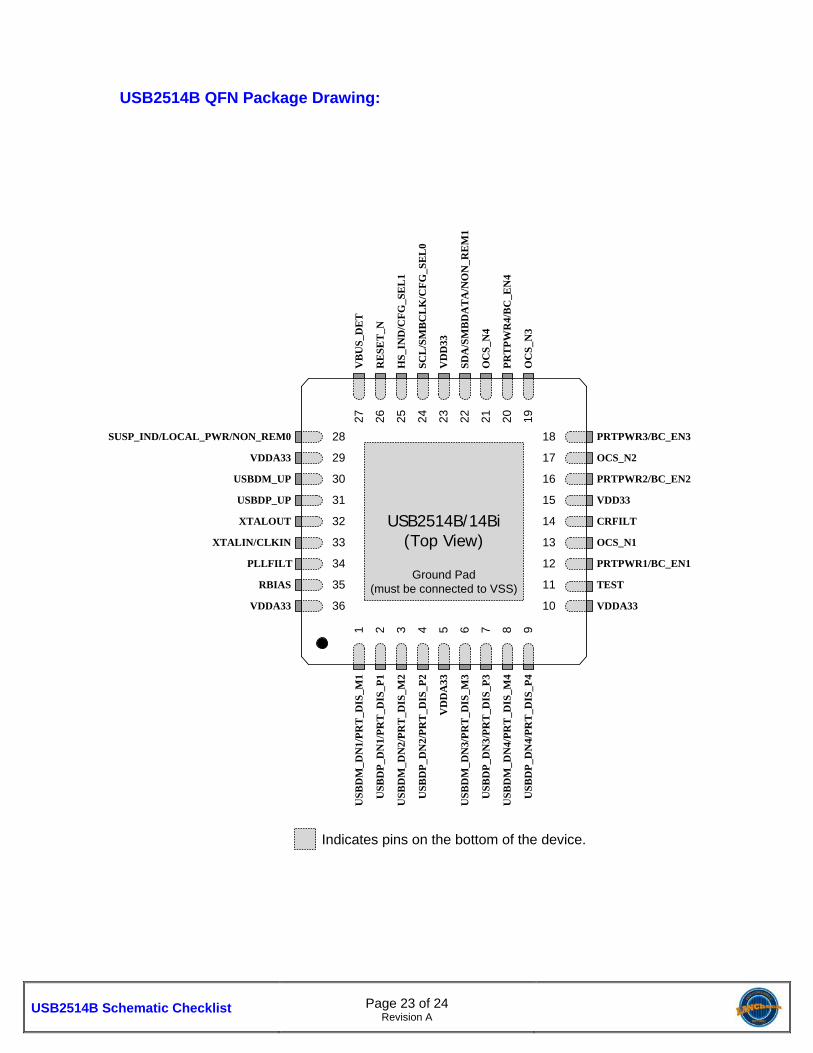
USB2514B QFN QuickCheck Pinout Table: Use the following table to check the USB2514B QFN shape in your schematic.
USB2514B QFN
Pin No. Pin Name Pin No. Pin Name
1 USBDM_DN1 / PRT_DIS_M1 19 OCS_N3
2 USBDP_DN1 / PRT_DIS_P1 20 PRTPWR4 / BC_EN4
3 USBDM_DN2 / PRT_DIS_M2 21 OCS_N4
4 USBDP_DN2 / PRT_DIS_P2 22 SDA / SMBDATA / NON_REM1
5 VDDA33 23 VDD33
6 USBDM_DN3 / PRT_DIS_M3 24 SCL / SMBCLK / CFG_SEL0
7 USBDP_DN3 / PRT_DIS_P3 25 HS_IND / CFG_SEL1
8 USBDM_DN4 / PRT_DIS_M4 26 RESET_N 9 USBDP_DN4 / PRT_DIS_P4 27 VBUS_DET
10 VDDA33 28 SUSP_IND / LOCAL_PWR / NON_REM0
11 TEST 29 VDDA33
12 PRTPWR1 / BC_EN1 30 USBDM_UP
13 OCS_N1 31 USBDP_UP
14 CRFILT 32 XTALOUT
15 VDD33 33 XTALIN / CLKIN
16 PRTPWR2 / BC_EN2 34 PLLFILT
17 OCS_N2 35 RBIAS
18 PRTPWR3 / BC_EN3 36 VDDA33
37
EDP Ground Connection
Exposed Die Paddle Ground
Pad on Bottom of Package
Notes:
USB2514B Schematic Checklist
Page 23 of 24
Revision A
USB2514B QFN Package Drawing:
Ground Pad(must be connected to VSS)
USB2514B/14Bi(Top View)
26
VD
D33
25
RE
SE
T_N
24
HS_
IND
/CF
G_S
EL
1
23
SC
L/S
MB
CL
K/C
FG
_SE
L0
22SD
A/S
MB
DA
TA
/NO
N_R
EM
1
21O
CS_
N4
20P
RT
PW
R4/
BC
_EN
4
19
VB
US_
DE
T27
OC
S_N
3
18
17
16
15
14
13
12
11
10 VDDA33
TEST
PRTPWR1/BC_EN1
OCS_N1
CRFILT
VDD33
PRTPWR2/BC_EN2
OCS_N2
PRTPWR3/BC_EN328
29
31
32
33
36
35
34
30
VDDA33
RBIAS
PLLFILT
XTALIN/CLKIN
XTALOUT
USBDP_UP
USBDM_UP
VDDA33
SUSP_IND/LOCAL_PWR/NON_REM0
1 2 3 4 5 6 7 8 9
USB
DM
_DN
1/P
RT
_DIS
_M1
US
BD
P_D
N1/
PR
T_D
IS_P
1
USB
DM
_DN
2/P
RT
_DIS
_M2
US
BD
P_D
N2/
PR
T_D
IS_P
2
VD
DA
33
USB
DM
_DN
3/P
RT
_DIS
_M3
US
BD
P_D
N3/
PR
T_D
IS_P
3
USB
DM
_DN
4/P
RT
_DIS
_M4
US
BD
P_D
N4/
PR
T_D
IS_P
4
Indicates pins on the bottom of the device.

USB2514B Schematic Checklist
Page 24 of 24
Revision A
Reference Material: 1. Microchip USB2514B Data Sheet; check web site for latest revision.
2. Microchip USB2514B CEB Schematic, Assembly EVB-USB2514; check web site for
latest revision.
3. Microchip USB2514B CEB PCB, Assembly EVB-USB2514; order PCB from web site.
4. Microchip USB2514B CEB PCB Bill of Materials, Assembly EVB-USB2514; check web site for latest revision.
5. CEB stands for Customer Evaluation Board.
6. Microchip USB2514B Reference Design, check web site for latest revision.
7. Microchip Reference Designs are schematics only; there are no associated PCBs.