scheme of instruction and syllabus (choice based...
TRANSCRIPT
M.Tech (VLSI)
Two Year (Four Semesters)
Scheme of Instruction and Syllabus
(Choice Based Grading System)
(With effect from 2015 – 2016 admitted batch onwards)
Department of Electronics and Communication Engineering
AU College of Engineering (Autonomous)
Visakhapatnam-530 003
2015

DEPARTMENT OF ELECTRONICS & COMMUNICATION ENGINEERING
A.U College of Engineering (A) Andhra University, Visakhapatnam
M.Tech (VLSI), Two Year (Four Semesters)
Scheme to be valid with effect from the admitted batch of 2015 – 2016
Semester – I
Subject code
Subject Title Credits
Pds/Week Sessionals Uni.Exam marks
Total Theory Lab
MTVL– 1.1 VLSI Design Techniques 4 4 - 30 70 100
MTVL – 1.2 Advanced Microprocessors and Microcontrollers
4 4 - 30 70 100
MTVL – 1.3 Analog IC design 4 4 - 30 70 100
MTVL – 1.4 Digital System Design 4 4 - 30 70 100
MTVL – 1.5 Elective – I a) Digital Signal Processing b) Application Specific Integrated
Circuit(ASIC) c) Hardware Software Co Design
4 4 - 30 70 100
MTVL – 1.6 Elective – II a) EMI/EMC b) VHDL Modeling of Digital
Systems c) EDA Tools
4 4 - 30 70 100
MTVL – 1.7 HDL Programming Laboratory 2 - 4 100 - 100
MTVL – 1.8 Seminar-I 2 - 2 100 - 100
Total 28 24 6 380 420 800
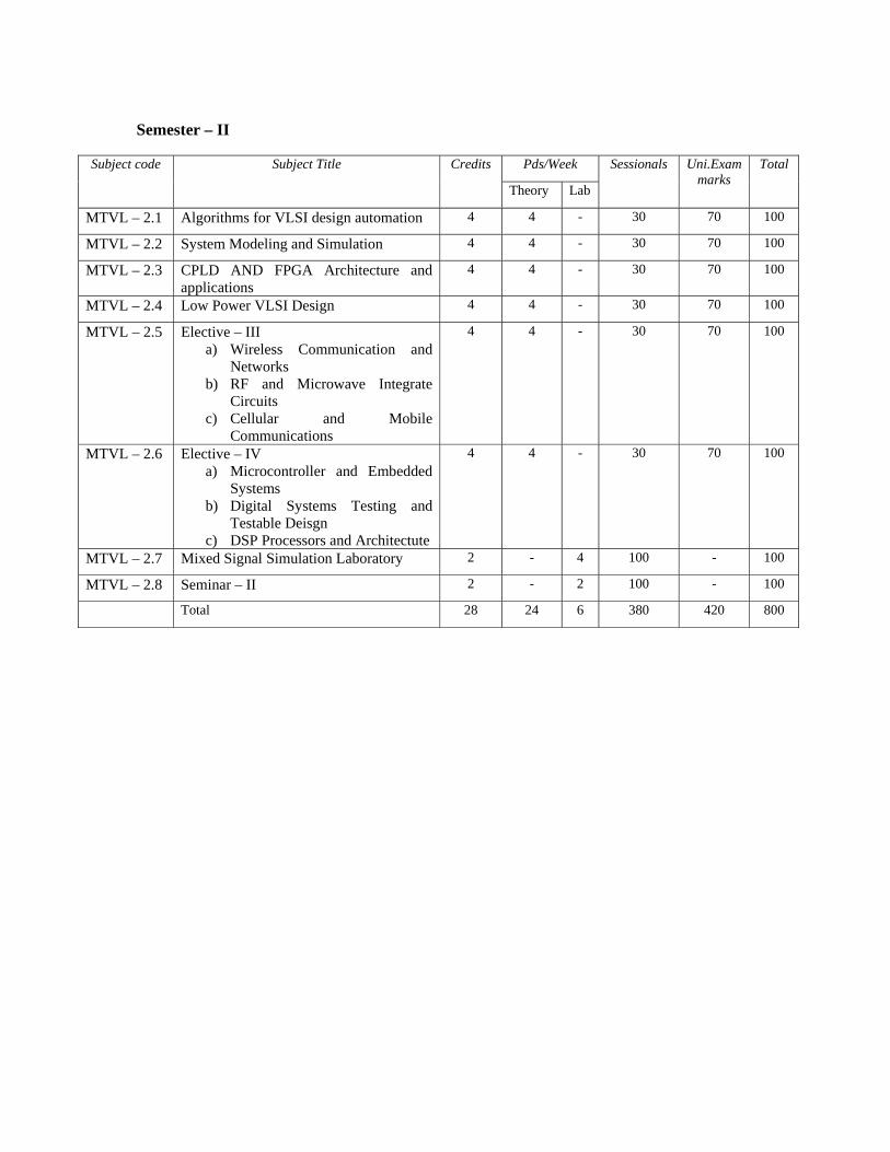
Semester – II
Subject code Subject Title Credits Pds/Week Sessionals Uni.Exam marks
Total
Theory Lab
MTVL – 2.1 Algorithms for VLSI design automation 4 4 - 30 70 100
MTVL – 2.2 System Modeling and Simulation 4 4 - 30 70 100
MTVL – 2.3 CPLD AND FPGA Architecture and applications
4 4 - 30 70 100
MTVL – 2.4 Low Power VLSI Design 4 4 - 30 70 100
MTVL – 2.5 Elective – III a) Wireless Communication and
Networks b) RF and Microwave Integrate
Circuits c) Cellular and Mobile
Communications
4 4 - 30 70 100
MTVL – 2.6 Elective – IV a) Microcontroller and Embedded
Systems b) Digital Systems Testing and
Testable Deisgn c) DSP Processors and Architectute
4 4 - 30 70 100
MTVL – 2.7 Mixed Signal Simulation Laboratory 2 - 4 100 - 100
MTVL – 2.8 Seminar – II 2 - 2 100 - 100
Total 28 24 6 380 420 800
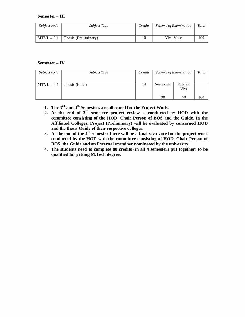
Semester – III
Subject code Subject Title Credits Scheme of Examination Total
MTVL – 3.1 Thesis (Preliminary) 10 Viva-Voce 100
Semester – IV
Subject code Subject Title Credits Scheme of Examination Total
MTVL – 4.1 Thesis (Final) 14 Sessionals
30
External Viva
70
100
1. The 3rd and 4th Semesters are allocated for the Project Work. 2. At the end of 3rd semester project review is conducted by HOD with the
committee consisting of the HOD, Chair Person of BOS and the Guide. In the Affiliated Colleges, Project (Preliminary) will be evaluated by concerned HOD and the thesis Guide of their respective colleges.
3. At the end of the 4th semester there will be a final viva voce for the project work conducted by the HOD with the committee consisting of HOD, Chair Person of BOS, the Guide and an External examiner nominated by the university.
4. The students need to complete 80 credits (in all 4 semesters put together) to be qualified for getting M.Tech degree.

VLSI DESIGN TECHNIQUES
Credits : 4
Subject Code : MTVL – 1.1 Max. Marks : 70 I – Semester Sessionals : 30
UNIT- I INTRODUCTION: Basic Principle of MOS Transistor, Introduction to Large Signal MOS Models (Long Channel) For Digital Design. UNIT –II THE MOS INVERTER, LAYOUT AND SIMULATION: Inverter principle, Depletion and enhancement load inverters, the basic CMOS inverter, transfer characteristics, logic threshold, Noise margins, and Dynamic behavior, Propagation Delay, Power Consumption. MOS SPICE Model, Device Characterization, Circuit Characterization, Interconnects and Simulation. MOS Device Layout, Transistor Layout, Inverter Layout, CMOS Digital Circuits Layout & Simulation UNIT- III COMBINATIONAL MOS LOGIC DESIGN: Static MOS design; Complementary MOS, Rationed logic, Pass Transistor logic, complex logic circuits, Dynamic MOS Design, Dynamic Logic Families and Performances.
UNIT –IV SEQUENTIAL MOS LOGIC DESIGN: Static Latches, Flip Flops and Registers, Dynamic Latches and Registers, CMOS Schmitt trigger, Monostable Sequential Circuits, Astable Circuits, Memory Design, ROM and RAM Cells Design UNIT –V INTERCONNECT AND CLOCK DISTRIBUTION: Interconnect Delays, Cross Talks, Clock Distribution. Introduction to Low‐ power Design, Input and Output Interface circuits. UNIT-VI BICMOS LOGIC CIRCUITS: Introduction, BJT Structure and Operation, Basic BiCMOS Circuit behavior, Switching Delay in BiCMOS Logic Circuits, BiCMOS Applications TEXT BOOKS:
1. Kang & Leblebigi “CMOS Digital IC Circuit Analysis & Design”- McGraw Hill, 2003
2. Rabey, “Digital Integrated Circuits Design”, Pearson Education, Second Edition, 2003
REFERENCE:
1. Weste and Eshraghian, “Principles of CMOS VLSI design” Addison-Wesley, 2002
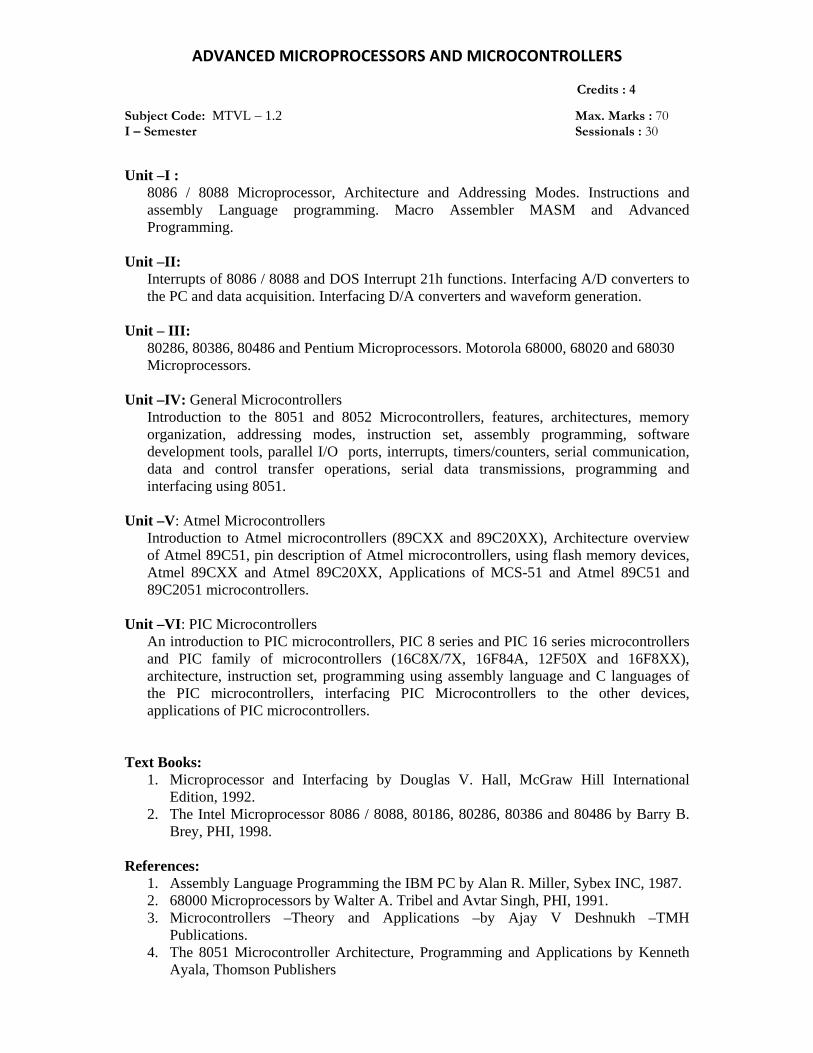
ADVANCED MICROPROCESSORS AND MICROCONTROLLERS
Credits : 4
Subject Code: MTVL – 1.2 Max. Marks : 70 I – Semester Sessionals : 30
Unit –I :
8086 / 8088 Microprocessor, Architecture and Addressing Modes. Instructions and assembly Language programming. Macro Assembler MASM and Advanced Programming.
Unit –II: Interrupts of 8086 / 8088 and DOS Interrupt 21h functions. Interfacing A/D converters to the PC and data acquisition. Interfacing D/A converters and waveform generation.
Unit – III: 80286, 80386, 80486 and Pentium Microprocessors. Motorola 68000, 68020 and 68030 Microprocessors.
Unit –IV: General Microcontrollers Introduction to the 8051 and 8052 Microcontrollers, features, architectures, memory organization, addressing modes, instruction set, assembly programming, software development tools, parallel I/O ports, interrupts, timers/counters, serial communication, data and control transfer operations, serial data transmissions, programming and interfacing using 8051.
Unit –V: Atmel Microcontrollers Introduction to Atmel microcontrollers (89CXX and 89C20XX), Architecture overview of Atmel 89C51, pin description of Atmel microcontrollers, using flash memory devices, Atmel 89CXX and Atmel 89C20XX, Applications of MCS-51 and Atmel 89C51 and 89C2051 microcontrollers.
Unit –VI: PIC Microcontrollers An introduction to PIC microcontrollers, PIC 8 series and PIC 16 series microcontrollers and PIC family of microcontrollers (16C8X/7X, 16F84A, 12F50X and 16F8XX), architecture, instruction set, programming using assembly language and C languages of the PIC microcontrollers, interfacing PIC Microcontrollers to the other devices, applications of PIC microcontrollers.
Text Books:
1. Microprocessor and Interfacing by Douglas V. Hall, McGraw Hill International Edition, 1992.
2. The Intel Microprocessor 8086 / 8088, 80186, 80286, 80386 and 80486 by Barry B. Brey, PHI, 1998.
References: 1. Assembly Language Programming the IBM PC by Alan R. Miller, Sybex INC, 1987. 2. 68000 Microprocessors by Walter A. Tribel and Avtar Singh, PHI, 1991. 3. Microcontrollers –Theory and Applications –by Ajay V Deshnukh –TMH
Publications. 4. The 8051 Microcontroller Architecture, Programming and Applications by Kenneth
Ayala, Thomson Publishers
ANALOG IC DESIGN
Credits : 4
Subject Code: MTVL – 1.3 Max. Marks : 70 I – Semester Sessionals : 30
UNIT- I INTEGRATED CIRCUIT DEVICES AND MODELLING: MOS Transistors, Advanced MOS Modeling, Bipolar Junction Transistors, Device Model Summary, SPICE Modelling Parameters. UNIT-II CURRENT MIRRORS AND SINGLE STAGE AMPLIFIERS: Simple CMOS Current Mirror, Common Source, Source-Follower, Common Gate Amplifier, High-Output-Impedance Current Mirrors and Bipolar Gain Stages, Frequency Response. UNIT –III OPERATIONAL AMPLIFIER DESIGN AND COMPENSATION: Two Stage CMOS Operational Amplifier, Feedback and Operational Amplifier Compensation, Comparator, Charge Injection Error, Latched Comparator and Bi CMOS Comparators. UNIT –IV ADVANCED CURRENT MIRRORS AND OPERATIONAL AMPLIFIERS: Advanced Current Mirror, Folded–Cascade Operational Amplifier, Current-Mirror Operational Amplifier, Fully Differential Operational Amplifiers, Common-Mode Feedback Circuits, Current-Feedback Operational Amplifiers. UNIT-V SAMPLE AND HOLD , SWITCHED-CAPACITOR CIRCUITS: MOS Sample-and-Hold Basics, CMOS Sample and Hold Circuits, Bipolar and BiCMOS Sample and Holds.Basic Operation and Analysis, First-Order and Biquad Filters, Charge Injection, Switched-Capacitor Gain Circuits, Correlated Double-Sampling Techniques, Other Switched-Capacitor circuits.
UNIT- VI DATA CONVERTERS: Ideal D/A & A/D Converters, Quantization Noise, Performance Limitations, Nyquist-Rate D/A Converters: Decoder Based Converters, Binary-Scaled Converters, Hybrid Converters, Nyquist-Rate A/D Converters, Integrating, Successive-Approximation, Cyclic Flash Type, Two-Step A/D Converters, Interpolating A/D Converters, Folding A/D Converters and Pipelined A/D Converters. Over Sampling with and without Noise Shaping, Digital Decimation Filter, Higher-Order Modulators, Bandpass Oversampling Converter
TEXT BOOKS:
1. I.D.A.JOHN & KEN MARTIN; Analog Integrated circuit design. John Wiley,1997
REFERENCE:
1. GREGOLIAN & TEMES: Analog MOS Integrated Circuits, John Wiley, 1986
DIGITAL SYSTEM DESIGN
Credits : 4
Subject Code : MTVL –1.4 Max. Marks : 70 I – Semester Sessionals : 30
UNIT – I DESIGN OF DIGITAL SYSTEMS: ASM charts, Hardware description language and control sequence method, Reduction of state tables, state assignments. UNIT – II SEQUENTIAL CIRCUIT DESIGN: design of Iterative circuits, design of sequential circuits using ROMs and PLAs, sequential circuit design using CPLD, FPGAs. UNIT – III FAULT MODELING: Fault classes and models – Stuck at faults, bridging faults, transition and intermittent faults. TEST GENERATION: Fault diagnosis of Combinational circuits by conventional methods – Path Sensitization technique, Boolean difference method, Kohavi algorithm. UNIT – IV TEST PATTERN GENERATION: D – algorithm, PODEM, Random testing, transition count testing, Signature analysis and testing for bridging faults. UNIT – V FAULT DIAGNOSIS IN SEQUENTIAL CIRCUITS: State identification and fault detection experiment. Machine identification, Design of fault detection experiment. UNIT – VI PROGRAMMING LOGIC ARRAYS AND ASYNCHRONOUS SEQUENTIAL MACHINE: Design using PLA’s, PLA minimization and PLA folding. Fault models, Test generation and Testable PLA design. Fundamental mode model, flow table, state reduction, minimal closed covers, races, cycles and hazards TEXT BOOKS: 1. Z. Kohavi – “Switching & finite Automata Theory” (TMH) 2. N. N. Biswas – “Logic Design Theory” (PHI) 3. Nolman Balabanian, Bradley Calson – “Digital Logic Design Principles” – Wily Student Edition 2004. REFRENCES: 1. M. Abramovici, M. A. Breues, A. D. Friedman – “Digital System Testing and Testable Design”, Jaico Publications 2. Charles H. Roth Jr. – “Fundamentals of Logic Design”. 3. Frederick. J. Hill & Peterson – “Computer Aided Logic Design” – Wiley 4th Edition. 4

Elective-I
DIGITAL SIGNAL PROCESSING
Credits : 4
Subject Code : MTVL – 1.5(a) Max. Marks : 70 I – Semester Sessionals : 30
Common with M.TECH (Radar and Microwave Engineering (MTRM-1.1)), M.Tech. (Electronic
Instrumentation(MTEI 1.1)
UNIT-I ADVANCED DIGITAL FILTER DESIGN TECHNIQUES: Multiple Band Optimal FIR Filters, Design of Filters with Simultaneous Constraints in Time and Frequency Response, Optimization Methods for Designing IR Filters, Comparison of Optimum FIR Filters and Delay Equalized Elliptic Filters. UNIT-II MULTI-RATE DIGITAL SIGNAL PROCESSING: The basic sample rate alteration – Time – Domain Characterization, Frequency – Domain Characterization: Cascade Equivalences, Filters in Sampling Rate Alteration Systems. UNIT-III DIGITAL FILTER BANKS AND OPTIMUM LINEAR FILTERS: Analysis of Digital Filter Banks and their Applications, Multi Level Filter Banks, Estimations of Spectra from Finite – Duration Observation of Signals , Forward and Backward Linear Prediction, AR Lattice and ARMA Lattice – Ladder Filters, Wieners Filters for Filtering on Prediction. UNIT-IV DIGITAL SIGNAL PROCESSING ALGORITHMS: The Goertzel Algorithm, The Chirp z -Transform Algorithm, The Levinson – Durbin Algorithms, The Schur Algorithm, and other Algorithms, Computations of the DFT, Concept of Tunable Digital Filters. UNIT-V SIGNAL PROCESSING HARDWARE AND FFT ARCHITECTURES AND PROCESSORS: Multipliers, Dividers, Different Forms of FIR Hardware, Multiplexing, DTTR, TDM to FDM Translator, Realization of Frequency Synthesizer. FFT Hardware Realization, Different FFT Architectures, Special FFT Processors, Convolvers, Lincoln Laboratory FDP and the Compatible Computer Configurations UNIT-VI APPLICATIONS OF DSP: Speech and DTMF Systems: Model of Speech Production, Speech Analysis –Synthesis System Vocoder Analyzers and Synthesizers, Linear Prediction of Speech and DTMF System.
TEXT BOOKS:
1. Theory and Applications of Digital Signal Processing by Lawrence R. Rabiner and Bernard Gold, PHI.
2. Digital Signal Processing. Principles, Algorithms, and Applications by John G. Proakis and Dimitris G. Manolakis, PHI, 1997.
REFERENCE:
1. Digital Signal Processing, A Computer – Based approach, by Sanjit K. Mitra, Tata Mc Graw-Hill, 1998
Elective-I
APPLICATION SPECIFIC INTEGRATED CIRCUITS (ASIC)
Credits : 4
Subject Code : MTVL – 1.5(b) Max. Marks : 70 I – Semester Sessionals : 30
Common with M.TECH (Radar and Microwave Engineering (MTRM-1.6(c))), M.Tech.
(Electronic Instrumentation (MTEI 1.6(c))
UNIT- I Introduction to ASICs – Types of ASICs, Design flow, Economics of ASICs, ASIC Cell Libraries, CMOS Logic, CMOS Design Rules, Logic Cells, I/O Cells, Cell Compilers.
UNIT- II ASIC Library Design – Transistors as resistors, Transistor Parasitic Capacitance, Logical Effort, Cell Design, Programmable ASICs, Programmable ASIC Logic Cells, Programmable ASIC I/O Cells, Programmable ASIC Interconnect, Programmable ASIC Design Software.
UNIT -III Low-level Design Entry, Schematic Entry, Low-Level Design Languages, PLA Tools, EDIF, An overview of VHDL and Verilog, Logic Synthesis, Simulation. ASIC Construction, Floor Planning and Placement.
UNIT- IV CMOS System Core Studies: Dynamic Warp Processors: Introduction, The Problem, The Algorithm, A Functional Overview, Detailed Functional Specification, Structural Floor Plan, Physical Design, Fabrication, Hierarchical Layout And Design Of Single Chip 32 Bit CPU: Introduction, Design Methodology, Technology Updatability And Layout Verification
UNIT -V Practical Realities and Ground Rules: Further Thoughts on Floor Plans/Layout, Floor Plan Layout of The Four Bit Processors, Input/output (I/O) Pads, “Real estate”, Further Thoughts on System Delays, Ground Rules for Successful Design, Scaling of MOS Circuits.
TEXTBOOK:
1. Application Specific Integrated Circuits by J.S. Smith, Addison Wesley, 1997.
REFERENCES:
1. Basic VLSI Design : Systems and Circuits, Doublas A. Pucknell & Kamran Eshraghian, Prentice Hall of India Private Ltd., New Delhi, 1989.
2. VLSI Design Techniques for analog and digital circuits, R.L. Geiger, P.E. Allen & N.R. Streder, McGraw Hill Int. 1990.
Elective-I
HARDWARE-SOFTWARE CO-DESIGN
Credits: 4
Subject Code : MTVL – 1.5(c) Max. Marks : 70 I – Semester Sessionals : 30
UNIT- I CO-DESIGN ISSUES: Co–design Models, Architectures, Languages, A Generic Co-Design Methodology,
UNIT- II CO-SYNTHESIS ALGORITHMS: Hardware –Software Synthesis Algorithms: Hardware –Software Partitioning, Distributed System Co-Synthesis
UNIT-III PROTOTYPING, EMULATION AND TARGET ARCHITECTURES : Prototyping and emulation techniques, Prototyping and emulation environments future developments in emulation and prototyping, architecture specialization techniques, system communication infrastructure, Target Architectures And Application System Classes, Architectures For Control Dominated System And Data Dominated Systems.
UNIT –IV COMPILATION TECHNIQUES AND TOOLS FOR EMBEDDED PROCESSOR ARCHITECTURES: Modern Embedded Architectures, Embedded Software Development Needs, Compilation Technologies, Practical Consideration in a Compiler Development Environment
UNIT- V DESIGN SPECIFICATION AND VERIFICATION: The Co-Design Computational Model, Concurrency, Co-Coordinating Concurrent Computations, Interfacing Components, Design Verification, Implementation Verification, Verification Tools, Interface Verification
UNIT- VI LANGUAGES FOR SYSTEM-LEVEL SPECIFICATION AND DESIGN: System Level Specification, Design Representation For System Level Synthesis, System Level Specification Languages Heterogeneous Specifications And Multi Language Co-Simulation, The Cosyma System And Lycos System.
TEXT BOOK:
1. Hardware/software co-design principles and practice, kluwer academic publishers
Elective-II
EMI / EMC
Credits : 4
Subject Code : MTVL – 1.6(a) Max. Marks : 70 I – Semester Sessionals : 30
Common with M.TECH (Radar and Microwave Engineering (MTRM-1.6(a))), M.E. (Electronic
Instrumentation(MTEI 1.6(a))
UNIT I INTRODUCTION, NATURAL AND NUCLEAR SOURCES OF EMI / EMC: Electromagnetic Environment, History, Concepts, Practical Experiences and Concerns, Frequency Spectrum Conservations. An Overview of EMI / EMC, Natural and Nuclear Sources of EMI. UNIT II EMI FROM APPARATUS, CIRCUITS AND OPEN AREA TEST SITES: Electromagnetic Emissions, Noise from Relays and Switches, Nonlinearities in Circuits, Passive Intermodulation , Cross Talk in Transmission Lines, Transients in Power Supply Lines, Electromagnetic Interference (EMI). Open -Area Test Sites and Measurements. UNIT III RADIATED AND CONDUCTED INTERFERENCE MEASUREMENTS AND ESD: Anechoic Chamber, TEM Cell, Giga-Hertz TEM Cell, Characterization of Conduction Currents / Voltages, Conducted EM Noise on Power Lines, Conducted EMI from Equipment, Immunity to Conducted EMI Detectors and Measurements. ESD, Electrical Fast Transients / Bursts, Electrical Surges. UNIT IV GROUNDING, SHIELDING, BONDING AND EMI FILTERS: Principles and Types of Grounding, Shielding and Bonding, Characterization of Filters, Power Line Filter Design. UNIT V CABLES, CONNECTORS, COMPONENTS AND EMC STANDARDS: EMI Suppression Cables, EMC Connectors, EMC Gaskets, Isolation Transformers, Opto-Isolators, National/ International EMC Standards. TEXT BOOKS:
1. Engineering Electromagnetic Compatibility by Dr. V.P. Kodali, IEEE Publication, Printed in India by S. Chand & Co. Ltd., New Delhi, 2000.
2. Electromagnetic Interference and Compatibility IMPACT series, IIT– Delhi, Modules1– 9.
REFERENCE :
1. Introduction to Electromagnetic Compatibility, Ny, John Wiley, 1992, by C.R. Pal.
Elective-II VHDL MODELLING OF DIGITAL SYSTEMS
Credits : 4
Subject Code : MTVL – 1.6(b) Max. Marks : 70 I – Semester Sessionals : 30
UNIT I INTRODUCTION An Overview Of Design Procedures Used For System Design Using CAD Tools. Design Entry. Synthesis, Simulation, Optimization, Place and Route. Design Verification Tools. Examples Using Commercial PC Based On VHDL Elements Of VHDL Top Down Design With VHDL Subprograms. Controller Description VHDL Operators. UNIT II BASIC CONCEPT IN VHDL Characterizing Hardware Languages, Objects And Classes, Signal Assignments, Concurrent And Sequential Assignments. Structural Specification Of Hardware: Parts Library Wiring Of Primitives, Wiring Interactive Networks, Modeling A Test Bench Binding Alternative Top Down Wiring. UNIT III DESIGN ORGANIZATIN AND PARAMETERIZATION Definition And Usage If Subprograms, Packaging Parts And Utilities, Design Parametrization, Design Configuration, Design Libraries, Utilities For High –Level Descriptions-Type Declaration And Usage, VHDL Operators, Subprogram Parameter Types And Overloading, Other Types And Type Related Issues, Predefined Attributes, User Defined Attributes, Packing Basic Utilities. UNIT IV DATA FLOW DESCRIPTION IN VHDL Multiplexing And Data Selection, State Machine Description, Open Collector Gates, Three State Bussing AGeneral Data Flow Circuit, Updating Basic Utilities. Behavioral Description Of Hardware: Process Statement Assection Statements, Sequential Wait Statements Formatted ASCII I/O Operators, MSI-Based Design. UNIT V CPU MODELLING FOR DESCRIPTION IN VHDL Parwan CPU, Behavioural Description Of Parawan, Bussing Structure, Data Flow Description Test Bench For The Parwan CPU. A More Realistic Parwan. Interface Design And Modeling. VHDL As A Modelling Language. TEXT BOOKS:
1. Z.NAWABI : VHDL Analysis And Modelling Of Digital Systems. (2/E), Mcgraw Hill, (1998)
REFERENCE:
1. PERRY : VHDL, (3/E) Mcgraw Hill 10

Elective –II
ELECTRONIC DESIGN AUTOMATION TOOLS Credits : 4
Subject Code : MTVL – 1.6(c) Max. Marks : 70 I – Semester Sessionals : 30
UNIT I IMPORTANT CONCEPTS IN VERILOG: Basics Of Verilog Language, Operators, Hierarchy, Procedures And Asignments, Timing Controls And Delay. Tasks And Functions Control Statements, Logic-Gate Modeling, Modeling Delay, Altering Parameters, other Verilog Features. UNIT II SYNTHESIS AND SIMULATION USING HDLS: Verilog And Logic Synthesis. VHDL And Logic Synthesis, Memory Synthesis,FSM Synthesis,Memory Synthesis, Performance-Driven Synthesis. Simulation-Types Of Simulation, Logic Systems Working Of Logic Simulation,Cell Models, Delay Models State Timing Analysis,Formal Verification, Switch-Level Simulation Transistor-Level Simulation. CAD Tools For Synthesis And Simulation Modelism And Leonardo Spectrum(Exemplar). UNIT III TOOLS FOR CIRCUIT DESIGN AND SIMULATION USING PSPICE: Pspice Models For Transistors, A/D & D/A Sample And Hold Circuits Etc, And Digital System Building Blocks, Design And Analysis Of Analog And Digital Circuits Using PSPICE. UNIT IV AN OVER VIEW OF MIXED SIGNAL VLSI DESIGN: Fundamentals Of Analog And Digital Simulation, Mixed Signal Simulator Configurations, Understanding Modeling, Integration To CAE Environments, Analyses Of Analog Circuits Eg.A/D, D/A Converters, Up And Down Converters, Companders Etc. UNIT V TOOLS FOR PCB DESIGN AND LAYOUT: An Overview Of High Speed PCB Design, Design Entry, Simulation And Layout Tools For PCB. Introduction To Orcad PCB Design Tools. TEXTBOOKS 1. J.Bhaskar, A Verilog Primer, BSP, 2003. 2. J.Bhaskar, A Verilog HDL Synthesis BSP, 2003 3. M.H.RASHID:SPICE FOR Circuits And Electronics Using PSPICE (2/E)(1992) Prentice
Hall. REFERENCES 1. ORCAD: Technical Reference Manual ,Orcad, USA. 2. SABER: Technical Reference Manual, Analogy Nic, USA. 3. M.J.S.SMITH :Aplication-Specific Integrated Circuits(1997). Addison Wesley 4. J.Bhaskar, A VHDL Synthesis Primer, BSP, 2003.
HDL PROGRAMMING LABORATORY
Credits: 2
Subject Code: MTVL – 1.7 Max. Marks: 50 I – Semester Sessionals: 50
1. Basic Gates
2. Adders
3. Subtractors
4. Full Adder Using Two Half Adders
5. Decoders
6. 4 Bit Binary Adder
7. Multiplexer
8. Encoder
9. Demultipluxers
10. Comparators
11. Flip flops
12. Counters
13. Shift registers
14. Mealy & Moore Machine for sequence detector
15. Implementation of ALU
16. RAM(4X4)
ALGORITHMS FOR VLSI DESIGN AUTOMATION Credits : 4
Subject Code : MTVL – 2.1 Max. Marks : 70 II – Semester Sessionals : 30
UNIT- I PRELIMINARIES: Introduction to Design Methodologies, Design Automation tools, Algorithmic Graph Theory, Computational Complexity, Tractable and Intractable Problems UNIT- II GENERAL PURPOSE MTHODS FOR COMBINATIONAL OPTIMIZATION: Backtracking, Branch and Bound, Dynamic Programming, Integer Linear Programming, LocalSearch, Simulated Annealing, Tabu search, Genetic Algorithms, Layout Compaction, Placement, Floorplanning and Routing Problems, Concepts and Algorithms. UNIT- III MODELLING AND SIMULATION: Gate Level Modeling and Simulation, Switch level modeling and simulation UNIT- IV LOGIC SYNTHESIS AND VERIFICATION: Basic issues and Terminology, Binary – Decision diagram, Two – Level Logic Synthesis, Hardware Models, Internal representation of the input algorithm, Allocation, Assignment and Scheduling, Some Scheduling Algorithms, Some aqspects ofAssignment problem, High – level Transformations UNIT –V PHYSICAL DESIGN AUTOMATION OF FPGA’S: FPGA technologies, Physical Design cycle for FPGA’s partitioning and Routing for segmented and staggered models. UNIT –VI PHYSICAL DESIGN AUTOMATION OF MCM’S: MCM technologies, MCM physical design cycle, Partitioning, Placement – Chip array based and full custom approaches, Routing Maze routing, Multiple stage routing, Topologic routing, Integrated Pin – Distribution and routing, routing and programmable MCM’s. TEXT BOOKS: 1. Algorithms for VLSI Design Automation, S.H.Gerez, WILEY student edition, John wiley & Sons (Asia) Pvt.Ltd. 1999. 2. Algorithms for VLSI Physical Design Automation, 3rd edition, Naveed Sherwani, Springer International Edition, 2005 REFERENCES: 1. Computer Aided Logical Design with Emphasis on VLSI – Hill & Peterson, Wiley, 1993 2. Modern VLSI Design: Systems on silicon – Wavne Wolf, Pearson Education Asia, 2nd Edition, 1998

SYSTEM MODELLING & SIMULATION Credits : 4
Subject Code : MTVL –2.2 Max. Marks : 70 II – Semester Sessionals : 30
UNIT I Basic Simulation Modeling : Systems, Models and Simulation, Discrete Event Simulation, Simulation of Single server queuing system, Simulation of Inventory System, Alternative approach to modeling and simulation. UNIT II SIMULATION SOFTWARE: Comparison of simulation packages with Programming Languages, Classification of Software, Desirable Software features, General purpose simulation packages – Arena, Extend and others, Object Oriented Simulation, Examples of application oriented simulation packages. UNIT III BUILDING SIMULATION MODELS AND MODELING TIME DRIVEN SYSTEMS: Guidelines for determining levels of model detail, Techniques for increasing model validity and credibility. Modeling input signals, delays, System Integration, Linear Systems, Motion Control models, numerical experimentation UNIT IV EXOGENOUS SIGNALS AND EVENTS: Disturbance signals, state machines, petri nets & analysis, System encapsulation, Probabilistic systems, Discrete Time Markov processes, Random walks, Poisson processes, the exponential distribution, simulating a poison process, Continuous – Time Markov processes. UNIT V EVEN DRIVEN MODELS: Simulation diagrams, Queuing theory, simulating queuing systems, Types of Queues, Multiple servers. UNIT VI SYSTEM OPTIMIZATION: System identification, Searches, Alpha/beta trackers, multidimensional optimization, modeling and simulation methodology. TEXT BOOKS: 1. System Modeling & Simulation, An introduction – Frank L.Severance, John Wiley&Sons, 2001. 2. Simulation Modeling and Analysis – Averill M.Law, W.David Kelton, TMH, 3rd Edition, 2003 REFERENCES:
1. Systems Simulation – Geoffery Gordon, PHI, 1978
CPLD AND FPGA ARCHITECTURE AND APPLICATIONS
Credits : 4
Subject Code : MTVL – 2.3 Max. Marks : 70 II – Semester Sessionals : 30
UNIT –I Programmable logic Devices: ROM, PLA, PAL, CPLD, FPGA – Features, Architectures, Programming, Applications and Implementation of MSI circuits using Programmable logic Devices. UNIT-II CPLDs: Complex Programmable Logic Devices: Altera series – Max 5000/7000 series and Altera FLEX logic-10000 series CPLD, AMD’s- CPLD (Mach 1 to 5), Cypress FLASH 370 Device technology, Lattice pLSI’s architectures – 3000 series – Speed performance and in system programmability. UNIT – III FPGAs: Field Programmable Gate Arrays- Logic blocks, routing architecture, design flow, technology mapping for FPGAs, Case studies Xilinx XC4000 & ALTERA’s FLEX 8000/10000 FPGAs: AT &T ORCA’s (Optimized Reconfigurable Cell Array): ACTEL’s ACT-1,2,3 and their speed performance UNIT-IV Finite State Machines (FSM): Top Down Design, State Transition Table , State assignments for FPGAs, Realization of state machine charts using PAL, Alternative realization for state machine charts using microprogramming, linked state machine, encoded state machine. Architectures Centered around non registered PLDs, Design of state machines centered around shift registers, One_Hot state machine, Petrinets for state machines-Basic concepts and properties, Finite State Machine-Case study UNIT- VI Design Methods and System Level Design: One –hot design method, Use of ASMs in one-hot design method, Applications of one hot design method, Extended Petri-nets for parallel controllers, Meta Stability, Synchronization, Complex design using shift registers.Controller, data path designing, Functional partition, Digital front end digital design tools for FPGAs & ASICs, System level design using mentor graphics EDA tool (FPGA Advantage), Design flow using CPLDs and FPGAs. UNIT – VIII Case studies: Design considerations using CPLDs and FPGAs of parallel adder cell, parallel adder sequential circuits, counters, multiplexers, parallel controllers. TEXT BOOKS: 1. Field Programmable Gate Array Technology - S. Trimberger, Edr, 1994, Kluwer Academic Publications. 2. Engineering Digital Design - RICHARD F.TINDER, 2nd Edition, Academic press. 3. Fundamentals of logic design-Charles H. Roth, 4th Edition Jaico Publishing House. REFERENCES: 1. Digital Design Using Field Programmable Gate Array, P.K.Chan & S. Mourad, 1994,
Prentice Hall. 2. Field programmable gate array, S. Brown, R.J.Francis, J.Rose ,Z.G.Vranesic, 2007, BSP.
LOW POWER VLSI DESIGN
Credits: 4
Subject Code: MTVL – 2.4 Max. Marks: 70 II – Semester Sessionals : 30
UNIT I LOW POWER DESIGN, AN OVER VIEW: Introduction to low- voltage low power design, limitations, Silicon-on-Insulator. UNIT II MOS/BiCMOS PROCESSES: Bi CMOS processes, Integration and Isolation considerations, Integrated Analog/Digital CMOS Process. Deep submicron processes, SOI CMOS, lateral BJT on SOI, future trends and directions of CMOS/BiCMOS processes. UNIT III DEVICE BEHAVIOR AND MODELING: Advanced MOSFET models, limitations of MOSFET models, bipolar models. Analytical and Experimental characterization of sub-half micron MOS devices, MOSFET in a Hybrid mode environment. UNIT IV CMOS AND Bi-CMOS LOGIC GATES: Conventional CMOS and BiCMOS logic gates. Performance evaluation UNIT V LOW- VOLTAGE LOW POWER LOGIC CIRCUITS: Comparison of advanced BiCMOS Digital circuits. ESD-free Bi CMOS, Digital circuit operation and comparative Evaluation UNIT VI LOW POWER LATCHES AND FLIP FLOPS: Evolution of Latches and Flip flops-quality measures for latches and Flip flops, Design perspective. TEXT BOOKS 1. CMOS/BiCMOS ULSI low voltage, low power by Yeo Rofail/ Gohl(3 Authors)-Pearson Education Asia 1st Indian reprint,2002 REFERENCES 1. Digital Integrated circuits, J.Rabaey PH. N.J 1996 2. CMOS Digital ICs sung-moKang and yusuf leblebici 3rd edition TMH2003 (chapter 11) 3. VLSI DSP systems, Parhi, John Wiley & sons, 2003 (chapter 17) 4. IEEE Trans Electron Devices, IEEE J.Solid State Circuits, and other National and
International Conferences and Symposia.
Elective-III
WIRELESS COMMUNICATIONS AND NETWORKS
Credits : 4
Subject Code : MTVL – 2.5(a) Max. Marks : 70 II – Semester Sessionals : 30
UNIT -I WIRELESS COMMUNICATION AND SYSTEM FUNDAMENTALS: Introduction to Wireless Communication Systems, Examples of Wireless Communications, Comparisons of Common Wireless Communication Systems, Trends in Cellular Radio and Personal Communications, Cellular Concepts, Frequency Reuse, Handoff Strategies, Interference and System Capacity, Trucking and Grade Of Service, Improving Coverage & Capacity In Cellular Systems.
UNIT-II MULTIPLE ACCESS TECHNIQUES FOR WIRELESS COMMUNICATION: FDMA, TDMA, SSMA (FHMA/CDMA/Hybrid Techniques) SDMA Technique (As Applicable to Wireless Communications), Packet Radio Access Protocols, CSMA Protocols, Reservation Protocols, Capture Effect in Packet Radio, Capacity of Cellular Systems.
UNIT-III WIRELESS NETWORKING: Introduction, Differences Between Wireless and Fixed Telephone Networks, Traffic Routing in Wireless Networks, Circuit Switching, Packet Switching, The X.25 protocol.
UNIT-IV Wireless Data Services, Cellular Digital Packet Data (CDPD), Advanced Radio Data Information Systems (ARDIS), RAM Mobile Data (RMD), Common Channel Signaling (CCS), Broad Band ISDN and ATM, Signaling System .No.7 (SS7), Network Services Part (NSP), SS7 User Part, Signaling Traffic in SS7, SS7 Services, Performance of SS7.
UNIT-V MOBILE IP AND WIRELESS APPLICATION PROTOCOL: Mobile IP Operation of Mobile IP, Co-located Address, Registration, Tunneling, WAP Architecture, Overview, WML Scripts, WAP Service, WAP Session protocol, Wireless Transaction, Wireless Datagram,Infrared LAN’s, Spread Spectrum LAN’s, Narrowband Microwave LAN’s, IEEE 802 Protocol Architecture, IEEE 802 Architecture and Services, 802. 11 Medium Access Controls, 802.11 Physical Layers.
UNIT-VI BLUE TOOTH AND MOBILE DATA NETWORKS: Overview, Radio Specification, Baseband Specification, Links Manager Specification, Logical Link Control and Adaptation Protocol, Introduction to WLL Technology, Introduction, and Data Oriented CDPD Network, GPRS and Higher Data Rates, Short Messaging Service in GSM, Mobile Application Protocol.

TEXT BOOKS:
1. Wireless communication and Networking -William Stallings, PHI, 2003 2. Wireless Communications, Principles, Practice - Theodore, S. Rappaport, PHI,
2nd Edition, 2002. REFERENCES:
1. Wireless Digital Communications-Karnilo feher,PHI, 1999.
2. Principles of Wireless Networks - Kavehpahlaven and P.Krishna Murthy, Pearson Education, 2002
Elective-III
RF AND MICROWAVE INTEGRATED CIRCUITS
Credits : 4
Subject Code : MTVL – 2.5(b) Max. Marks : 70 II – Semester Sessionals : 30
UNIT-I Analysis and Design of RF and Microwave Lines – Review of Transmission Lines, Parallel Plate Transmission Lines, Low -Frequency Solution, High Frequency Solution,
UNIT–II Strip Line And Micro Strip Transmission Lines, Low Frequency Solution, High Frequency Properties Of Micro Slot Line, Co Planer Wave Guides, Spiral Inductors – Capacitors.
UNIT–III Microstrip/Stripline Based Filters. Resonators, Plane Shifters, Micro Strip Based Gyrators, Circulators And Isolators, Directional Couplers.
UNIT–IV Microwave Active Devices – Microwave Transistors, GaAs FETS (Structures, Equivalent Circuit), Low Noise Amplifiers, Power Amplifiers, Oscillators, Detect5ors, Mixers, Modulators and Switches.
UNIT-V Technology of MICS: Deposition Techniques – Vacuum Evaporation – Vacuum Sputtering Ion Planting. MBE (molecular Beam Epitaxy) – Photo Lithography, Mask Preparation, Thick Film Technology, GaAs Technology.
UNIT–VI MIC Packaging: Component Attachment, Bonding Techniques, Solder Reflow Techniques, Input/Output Terminations, Testing.
TEXT BOOKS:
1. Microwave Engineering – Prof. G.S.N Raju, I.K. International Publication. 2. I.Kneppo and J. Fabian, “Microwave Integrated Circuit”, London: Chapman & Hall,
(1994). 3. M.W.Medley, “Microwave and RF circuit: Analysis, Synthesis and Design”, Artech
House, (1993).
REFERENCES:
1. R.Goyal, “Monolithic Microwave Integrated Circuit: Technology & Design”, Artech House, (1989).
2. Y.Konishi, “Microwave Integrated Circuit”, Dekker, New York: Marcel Dekker, (1991).
Elective-III
CELLULAR AND MOBILE COMMUNICATIONS
Credits: 4
Subject Code : MTVL – 2.5(c) Max. Marks : 70 II – Semester Sessionals : 30
Common with M.TECH (Radar and Microwave Engineering (MTRM-2.3) )
UNIT- I Introduction to Wireless communications, examples of wireless communication system, the Cellular concept and system design fundamentals, Frequency reuse, channel assignment strategies, handoff strategies, Interference and system capacity, Trunk and grade services, Methods for improving coverage and capacity in cellular system
UNIT- II Multiple access techniques for wireless communications FDMA, TDMA, Spread spectrum techniques, SDMA, Packet Radio, CSMA , Capacity of cellular CDMA with multiple cells and capacity of SDMA. UNIT-III Wireless systems and standards, AMPS, IS – 94, GSM traffic, Examples of GSM cell, Frame structure of GSM cell, Details of forward and reverse CDMA channels. UNIT-IV Personal access communication systems, personal Mobile satellite communications, Integrating Geo, LEO MEO satellite and terrestrial mobile systems, Rake receiver and Advanced Rake receiver, UNIT-V Mobile Radio Propagation, Large scale path loss, Reflection, Diffraction, Scattering, Outdoor and Indoor Propagation models, small signal fading and multi path, measurement of small scale path loss, parameters and multi path channels, fading due to multi path, fading effect due to Doppler spread, small scale fading models, equalization, Diversity. Text Book:
1. Mobile cellular communication by Gottapu Sasibhushan Rao, PERSON International, 2012.
2. Wireless communications Principles and Practice, Second Editions, THEODORE S.REPPAPORT.
REFERENCES:
1. Wireless Digital Communications, DR. KAMILO FEHER. 2. Electronic Communication system, WAYNE ToMASI. 3. Wireless Communications, SANJY SHARMS
Elective-IV
MICROCONTROLLERS AND EMBEDDED SYSTEMS
Credits: 4
Subject Code : MTVL – 2.6(a) Max. Marks : 70 II – Semester Sessionals : 30
Common with M.TECH (Radar and Microwave Engineering (MTRM-2.6(b))),M.Tech
(Electronic Instrumentation (MTEI 2.6(b))
UNIT-1 INTRODUCTION: Embedded Systems overview, Design Challenge, Processor Technology, IC Technology, Design Technology, Trade-offs.
UNIT-II CUSTOM SINGLE-PURPOSE PROCESSORS (HARDWARE): Introduction, Combinational logic, Sequential logic, Custom Single-Purpose Processor Design, RT-Level Custom Single-Purpose Processor Design, Optimizing Custom Single-Purpose Processors.
UNIT-III GENERAL PURPOSE PROCESSORS (SOFTWARE): Introduction, Basic Architecture, Operation, Programmer’s view, Development Environment, Application-Specific Instruction-set Processors, Selecting a Microprocessor.
UNIT-IV MEMORY: Introduction, Memory types, Memory Hierarchy and Cache, Advanced Memory Interfacing: Communication Basics, Memory Access, I/O addressing, Interrupts, DMA, Arbitration, Multilevel Architecture, Protocols.
UNIT-V
MICROCONTROLLERS: Review of 8051 Microcontroller Architecture & Programming.Peripherals: Timers, Counters and Watchdog Timers, UART, Pulse width Modulators, LCD Controllers, Stepper Motor Controllers, Analog to Digital Converters, Real-Time Clocks. Digital Camera Introduction, Specifications, Design.
UNIT-VI STATE MACHINE AND CONCURRENT PROCESS MODELS: Introduction, Models Vs Languages, Text Vs Graphics, Textual Languages Vs Graphical Languages, An Example, A Basic State Machine Model, FSM with Data Path Model, FSMD Using State Machines, Concurrent Process Model, Communication among Processes.
TEXT BOOKS:
1. Embedded System Design: A Unified Hardware/Software Introduction By Frank vahid / Tony Givargis John wiley & sons
2. The 8051 Microcontroller & Embedded Systems By Muhammad Ali Mazidi & Janice Gillispie Mazidi PHI
REFERENCES: 1. Embedded Systems Architecture, Programming and Design By RajKamal TMH 2. Embedded Software Priner By Simon. 3. The 8051 Microcontroller: Architecture, Programming & Applications. By Kenneth J.Ayala Penram International. 2nd edn.
Elective-IV
DIGITAL SYSTEMS TESTING AND TESTABLE DESIGN
Credits: 4
Subject Code: MTVL – 2.6(b) Max. Marks: 70 II – Semester Sessionals: 30
UNIT- I INTRODUCTION TO TEST AND DESIGN FOR TESTABILITY (DFT) SIMULATIONS: Fundamentals, Modeling Digital Circuits at Logic Level, Register Level and Structural Models. Levels of Modeling. Types of Simulation, Delay models, Element evaluation, Hazard detection, Gate level event driven simulation.
UNIT- II FAULT MODELING: Logic fault models, Fault detection and redundancy, Fault equivalence and fault location. Single stuck and multiple stuck – Fault models. Fault simulation applications, General techniques for combinational circuits.
UNIT- III TESTING FOR SINGLE STUCK FAULTS (SSF): Automated Test Pattern Generation (ATPG/ATG) For SSFs In Combinational And Sequential Circuits ,Functional Testing With Specific Fault Models .Vector Simulation – ATPG Vectors ,Formats, Compaction And Compression ,Selecting ATPG Tool
UNIT- IV DESIGN FOR TESTABILITY: Testability Trade-Offs, Techniques. Scan Architectures And Testing – Controllability And Absorbability, Generic Boundary Scan, Full Integrated Scan, Storage Cells For Scan Design. Board Level And System Level DFT Approaches.
UNIT- V BOUNDARY SCANS STANDARDS AND BIST: Compression Techniques – Different Techniques, Syndrome Test And Signature Analysis, BIST Concepts And Test Pattern Generation. Specific BIST Architectures CSBL, BEST, RTS, LOCST, STUMPS,CBIST, CEBS, RTD, SST,CATS, CSTP, BILBO. Brief Ideas on Some Advanced BIST Concepts And Design for Self-Test at Board Level.
UNIT- VI MEMORY BIST (MBIST): Memory Test Architectures And Techniques – Introduction to Memory Test, Types Of Memories And Integration, Embedded Memory Testing Model, Memory Test Requirements for MBIST, Brief Ideas on Embedded Core Testing, Introduction to Automatic In Circuit Testing (ICT), JTAG Testing Features.
TEXT BOOKS:
1. Miron Abramovici, Melvin A. Breur, Arthur D.Friedman, Digital Systems Testing and Testable Design, Jaico Publishing House,2001
2. Alfred Crouch, Design for Test for Digital ICs and Embedded core systems, Prentice Hall.
REFERENCES:
1. Robert J.Feugate, Jr., Steven M.Mentyn, Introduction to VLSI Testing ,Prentice Hall,Englehood Cliffs,1998

Elective-IV
DSP PROCESSORS AND ARCHITECTURES Credits: 4
Subject Code: MTVL – 2.6(c) Max. Marks: 70 II – Semester Sessionals: 30
UNIT I INTRODUCTION TO DIGITAL SIGNAL PROCESING Introduction, A Digital signal-processing system, The sampling process, Discrete time sequences Discrete Fourier Transform (DFT) and Fast Fourier Transform (FFT), Linear time-invariant systems, Digital filters, Decimation and interpolation, Analysis and Design tool for DSP Systems MATLAB, DSP using MATLAB. UNIT II COMPUTATIONAL ACCURACY IN DSP IMPLEMENTATIONS Number formats for signals and coefficients in DSP systems, Dynamic Range and Precision, Sources of error in DSP implementations, A/D Conversion errors, DSP Computational errors, D/A Conversion Errors, Compensating filter. UNIT III ARCHITECTURES FOR PROGRAMMABLE DSP DEVICES AND EXECUTION Basic Architectural features, DSP Computational Building Blocks, Bus Architecture and Memory, Data Addressing Capabilities, Address Generation Unit, Programmability and Program Execution, Speed Issues, Features for External interfacing, Hardware looping, Interrupts, Stacks, Relative Branch support, Pipelining and Performance, Pipeline Depth, Interlocking, Branching effects, Interrupt effects, Pipeline Programming models UNIT IV PROGRAMMABLE DIGITAL SIGNAL PROCESSORS Commercial Digital signal-processing Devices, Data Addressing modes of TMS320C54XX DSPs, Data Addressing modes of TMS320C54XX Processors, Memory space of TMS320C54XX Processors, Program Control, TMS320C54XX instructions and Programming, On-Chip Peripherals, Interrupts of TMS320C54XX processors, Pipeline Operation of TMS320C54XX Processors. UNIT V IMPLEMENTATIONS OF BASIC DSP ALGORITHMS AND FFT ALGORITHMS The Q-notation, FIR Filters, IIR Filters, Interpolation Filters, Decimation Filters, PID Controller, Adaptive Filters, 2-D Signal Processing, An FFT Algorithm for DFT Computation, A Butterfly Computation, Overflow and scaling, Bit-Reversed index generation, An 8-Point FFT implementation on the TMS320C54XX, Computation of the signal spectrum UNIT VI INTERFACING MEMORY AND I/O PERIPHERALS TO PROGRAMMABLE DSP DEVICES Memory space organization, External bus interfacing signals, Memory interface, Parallel I/O interface, Programmed I/O, Interrupts and I/O, Direct memory access (DMA). A Multichannel buffered serial port (McBSP), McBSP Programming, a CODEC interface circuit, CODEC programming, A CODEC-DSP interface example.
TEXT BOOKS: 1. Digital Signal Processing – Avtar Singh and S. Srinivasan, Thomson Publications, 2004. 2. DSP Processor Fundamentals, Architectures & Features – Lapsley et al. S. Chand & Co,
2000. REFERENCES: 1. Digital Signal Processors, Architecture, Programming and Applications – B. Venkata
Ramani and M.Bhaskar, TMH, 2004. 2. Digital Signal Processing – Jonatham Stein, John Wiley, 2005.
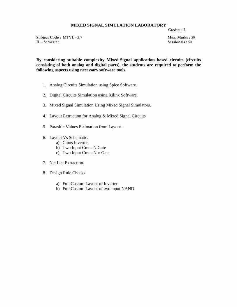
MIXED SIGNAL SIMULATION LABORATORY Credits : 2
Subject Code : MTVL –2.7 Max. Marks : 50 II – Semester Sessionals : 50
By considering suitable complexity Mixed-Signal application based circuits (circuits consisting of both analog and digital parts), the students are required to perform the following aspects using necessary software tools.
1. Analog Circuits Simulation using Spice Software.
2. Digital Circuits Simulation using Xilinx Software.
3. Mixed Signal Simulation Using Mixed Signal Simulators.
4. Layout Extraction for Analog & Mixed Signal Circuits.
5. Parasitic Values Estimation from Layout.
6. Layout Vs Schematic. a) Cmos Inverter b) Two Input Cmos N Gate c) Two Input Cmos Nor Gate
7. Net List Extraction.
8. Design Rule Checks.
a) Full Custom Layout of Inverter b) Full Custom Layout of two input NAND
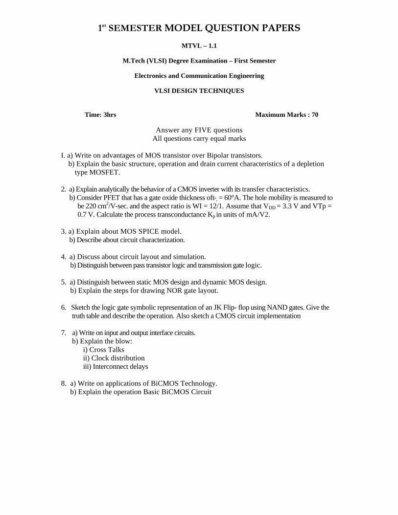
1st SEMESTER MODEL QUESTION PAPERS
MTVL – 1.1
M.Tech (VLSI) Degree Examination – First Semester
Electronics and Communication Engineering
VLSI DESIGN TECHNIQUES
Time: 3hrs Maximum Marks : 70
Answer any FIVE questions All questions carry equal marks
I. a) Write on advantages of MOS transistor over Bipolar transistors. b) Explain the basic structure, operation and drain current characteristics of a depletion
type MOSFET. 2. a) Explain analytically the behavior of a CMOS inverter with its transfer characteristics. b) Consider PFET that has a gate oxide thickness oft°, = 60°A. The hole mobility is measured to
be 220 cm2/V-sec. and the aspect ratio is WI = 12/1. Assume that VDD = 3.3 V and VTp = 0.7 V. Calculate the process transconductance Kp in units of mA/V2.
3. a) Explain about MOS SPICE model. b) Describe about circuit characterization. 4. a) Discuss about circuit layout and simulation. b) Distinguish between pass transistor logic and transmission gate logic. 5. a) Distinguish between static MOS design and dynamic MOS design. b) Explain the steps for drawing NOR gate layout. 6. Sketch the logic gate symbolic representation of an JK Flip- flop using NAND gates. Give the
truth table and describe the operation. Also sketch a CMOS circuit implementation 7. a) Write on input and output interface circuits. b) Explain the blow:
i) Cross Talks ii) Clock distribution iii) Interconnect delays
8. a) Write on applications of BiCMOS Technology. b) Explain the operation Basic BiCMOS Circuit
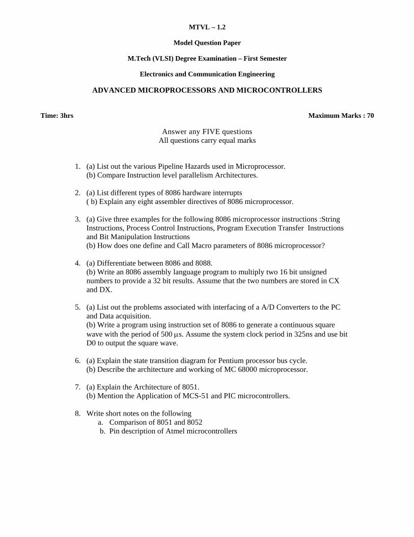
MTVL – 1.2
Model Question Paper
M.Tech (VLSI) Degree Examination – First Semester
Electronics and Communication Engineering
ADVANCED MICROPROCESSORS AND MICROCONTROLLERS
Time: 3hrs Maximum Marks : 70
Answer any FIVE questions All questions carry equal marks
1. (a) List out the various Pipeline Hazards used in Microprocessor. (b) Compare Instruction level parallelism Architectures.
2. (a) List different types of 8086 hardware interrupts ( b) Explain any eight assembler directives of 8086 microprocessor.
3. (a) Give three examples for the following 8086 microprocessor instructions :String Instructions, Process Control Instructions, Program Execution Transfer Instructions and Bit Manipulation Instructions (b) How does one define and Call Macro parameters of 8086 microprocessor?
4. (a) Differentiate between 8086 and 8088. (b) Write an 8086 assembly language program to multiply two 16 bit unsigned numbers to provide a 32 bit results. Assume that the two numbers are stored in CX and DX.
5. (a) List out the problems associated with interfacing of a A/D Converters to the PC and Data acquisition. (b) Write a program using instruction set of 8086 to generate a continuous square wave with the period of 500 µs. Assume the system clock period in 325ns and use bit D0 to output the square wave.
6. (a) Explain the state transition diagram for Pentium processor bus cycle. (b) Describe the architecture and working of MC 68000 microprocessor.
7. (a) Explain the Architecture of 8051. (b) Mention the Application of MCS-51 and PIC microcontrollers.
8. Write short notes on the following a. Comparison of 8051 and 8052
b. Pin description of Atmel microcontrollers

MTVL – 1.3
Model Question Paper
M.Tech (VLSI) Degree Examination – First Semester
Electronics and Communication Engineering
ANALOG IC DESIGN
Time: 3hrs Maximum Marks : 70
Answer any FIVE questions
All questions carry equal marks
1. a) Derive the relationship between Ids and Vds for an NMOS device. b) Compare CMOS and bipolar technologies. 2. a) What is current boosting? Explain the common source amplifier. b) Give the reasons why an open loop op-amp is not suitable for linear applications with
necessary analysis. 3. a) Explain the current mirror operational amplifier. b) What are BiCMOS comparators? Derive the expression for Latch time in latched
comparators. 4. a) Explain fully differential folded cascade OPAMP. b) Design a practical integration circuit using OP-AMP and explain its frequency response 5. a) Explain CMOS sample and hold ckt in detail. b) Explain Differential Operational Amplifier 6. a) Consider the sample and hold ckt shown in figure where Vth is a 20 MHz band limited
signal with a 2-Vm amplitude. Assume that Puk is 100 MHz square wave having a peak amplitude of + 2.5 V with linear rise and fall times of 1.5 ns. What is maximum uncertainity of the sampling time.
b) Write short notes on (i) Acquisition time ii) Aperture time 7. (a) What are the performance limitations for A/D and D/A converters? Explain. (b) Explain the first order active RC filters and first order switched capacitor filters. 8. Write short notes on i) Digital Decimation Fillets ii) Over sampling with and without noise shaping

MTVL-1.4
Model Question Paper
M.Tech (VLSI) Degree Examination – First Semester
Electronics and Communication Engineering
DIGITAL SYSTEM DESIGN
Time: 3hrs Maximum Marks : 70
Answer any FIVE questions
All questions carry equal marks
1. a) Describe about Hardware description language. b) What is a logic probe? What for it used and list different internal digital IC
faults? 2. a) How does the ASM chart differ from a software flow chart? b) Distinguish between
CPLD and FPGA.
3. a) Discuss in detail about reduction of state tables and state assignments. b) Explain about (i) Stuck at faults, (ii) Bridge faults, (iii) Temporary faults. 4. a) Explain the delay modeling for Gates with neat diagrams. b) Explain about D-algorithm in combinational circuits. 5. a) With example, explain the principle of Boolean difference method. b) Distinguish between PLA and PAL. 6. a) Design and realize a PLA circuit with four inputs Xi, X2, X3 and X4 and seven
outputs 1)1, P2, MI, 1112, m3, m4 and m5 that receives BCD code words and generates the corresponding code words.
b) Distinguish between Mealy and Moore Machines. 7. a) Implement the Hazard free circuit for the following function: f (A,B,C ,D)=. ABC + ABC +Ci5 + AC b) Discuss about BIST scheme for PLD and CPI,D's 8. Write short notes on any TWO of the following:
(i) Design for Testability (ii) PLA folding Algorithm COMPACT (iii )Kohari algorithm
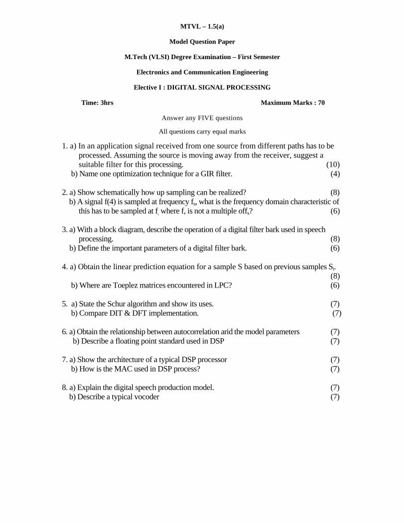
MTVL – 1.5(a)
Model Question Paper
M.Tech (VLSI) Degree Examination – First Semester
Electronics and Communication Engineering
Elective I : DIGITAL SIGNAL PROCESSING
Time: 3hrs Maximum Marks : 70
Answer any FIVE questions
All questions carry equal marks
1. a) In an application signal received from one source from different paths has to be processed. Assuming the source is moving away from the receiver, suggest a suitable filter for this processing. (10)
b) Name one optimization technique for a GIR filter. (4) 2. a) Show schematically how up sampling can be realized? (8) b) A signal f(4) is sampled at frequency fs, what is the frequency domain characteristic of
this has to be sampled at f, where f, is not a multiple offs? (6) 3. a) With a block diagram, describe the operation of a digital filter bark used in speech
processing. (8) b) Define the important parameters of a digital filter bark. (6) 4. a) Obtain the linear prediction equation for a sample S based on previous samples Si. (8) b) Where are Toeplez matrices encountered in LPC? (6) 5. a) State the Schur algorithm and show its uses. (7) b) Compare DIT & DFT implementation. (7) 6. a) Obtain the relationship between autocorrelation arid the model parameters (7) b) Describe a floating point standard used in DSP (7) 7. a) Show the architecture of a typical DSP processor (7) b) How is the MAC used in DSP process? (7) 8. a) Explain the digital speech production model. (7) b) Describe a typical vocoder (7)
MTVL-1.6(a)
Model Question Paper
M.Tech (VLSI) Degree Examination – First Semester
Electronics and Communication Engineering
Elective – II : EMI / EMC
(Common with R&M (MTRM-1.6(a)), Electronic Instrumentation (MTEI-1.6(a)))
Time: 3hrs Maximum Marks : 70
Answer any FIVE questions
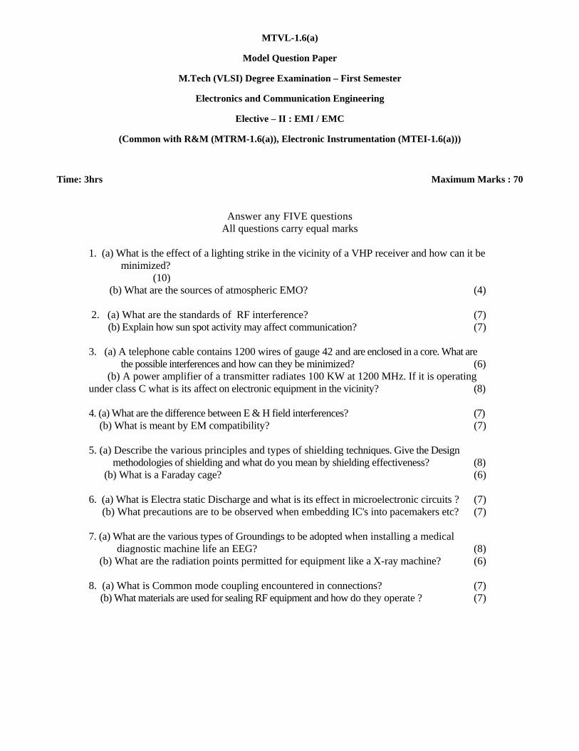
All questions carry equal marks 1. (a) What is the effect of a lighting strike in the vicinity of a VHP receiver and how can it be
minimized? (10)
(b) What are the sources of atmospheric EMO? (4) 2. (a) What are the standards of RF interference? (7) (b) Explain how sun spot activity may affect communication? (7) 3. (a) A telephone cable contains 1200 wires of gauge 42 and are enclosed in a core. What are
the possible interferences and how can they be minimized? (6) (b) A power amplifier of a transmitter radiates 100 KW at 1200 MHz. If it is operating under class C what is its affect on electronic equipment in the vicinity? (8) 4. (a) What are the difference between E & H field interferences? (7) (b) What is meant by EM compatibility? (7) 5. (a) Describe the various principles and types of shielding techniques. Give the Design
methodologies of shielding and what do you mean by shielding effectiveness? (8) (b) What is a Faraday cage? (6) 6. (a) What is Electra static Discharge and what is its effect in microelectronic circuits ? (7) (b) What precautions are to be observed when embedding IC's into pacemakers etc? (7) 7. (a) What are the various types of Groundings to be adopted when installing a medical
diagnostic machine life an EEG? (8) (b) What are the radiation points permitted for equipment like a X-ray machine? (6) 8. (a) What is Common mode coupling encountered in connections? (7) (b) What materials are used for sealing RF equipment and how do they operate ? (7)
MTVL-1.6(b)
Model Question Paper
M.Tech (VLSI) Degree Examination – First Semester
Electronics and Communication Engineering
Elective – II : VHDL MODELLING OF DIGITAL SYSTEMS
Time: 3hrs Maximum Marks : 70
Answer any FIVE questions All questions carry equal marks
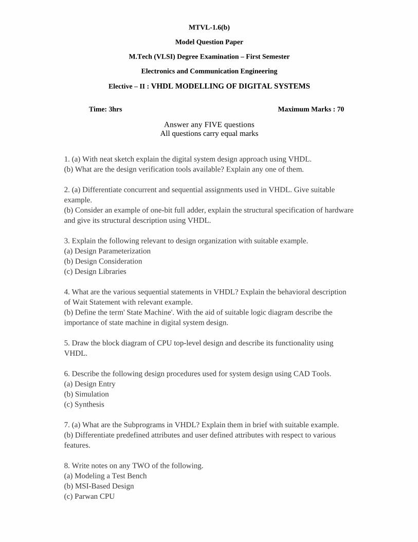
1. (a) With neat sketch explain the digital system design approach using VHDL. (b) What are the design verification tools available? Explain any one of them. 2. (a) Differentiate concurrent and sequential assignments used in VHDL. Give suitable example. (b) Consider an example of one-bit full adder, explain the structural specification of hardware and give its structural description using VHDL. 3. Explain the following relevant to design organization with suitable example. (a) Design Parameterization (b) Design Consideration (c) Design Libraries 4. What are the various sequential statements in VHDL? Explain the behavioral description of Wait Statement with relevant example. (b) Define the term' State Machine'. With the aid of suitable logic diagram describe the importance of state machine in digital system design. 5. Draw the block diagram of CPU top-level design and describe its functionality using VHDL. 6. Describe the following design procedures used for system design using CAD Tools. (a) Design Entry (b) Simulation (c) Synthesis 7. (a) What are the Subprograms in VHDL? Explain them in brief with suitable example. (b) Differentiate predefined attributes and user defined attributes with respect to various features. 8. Write notes on any TWO of the following. (a) Modeling a Test Bench (b) MSI-Based Design (c) Parwan CPU
MTVL-1.6(c)
Model Question Paper
M.Tech (VLSI) Degree Examination – First Semester
Electronics and Communication Engineering
Elective – II : ELECTRONIC DESIGN AUTOMATION TOOLS
Time: 3hrs Maximum Marks : 70
Answer any FIVE questions All questions carry equal marks
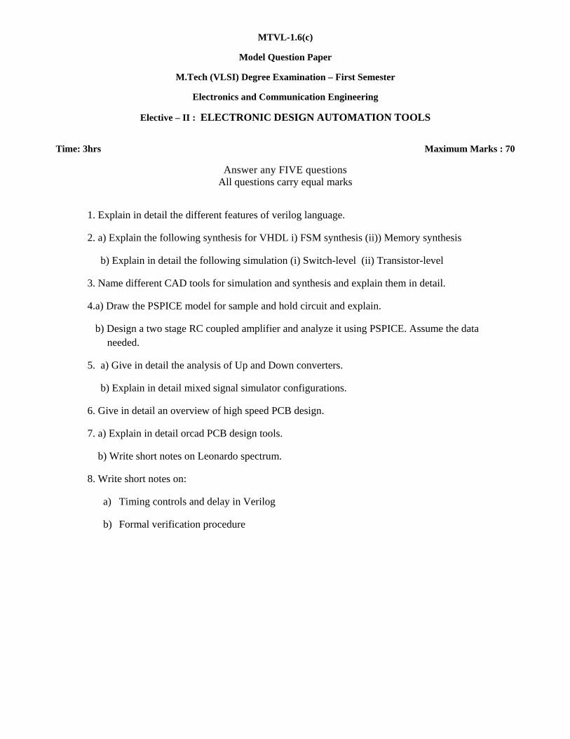
1. Explain in detail the different features of verilog language.
2. a) Explain the following synthesis for VHDL i) FSM synthesis (ii)) Memory synthesis
b) Explain in detail the following simulation (i) Switch-level (ii) Transistor-level
3. Name different CAD tools for simulation and synthesis and explain them in detail.
4.a) Draw the PSPICE model for sample and hold circuit and explain.
b) Design a two stage RC coupled amplifier and analyze it using PSPICE. Assume the data needed.
5. a) Give in detail the analysis of Up and Down converters.
b) Explain in detail mixed signal simulator configurations.
6. Give in detail an overview of high speed PCB design.
7. a) Explain in detail orcad PCB design tools.
b) Write short notes on Leonardo spectrum.
8. Write short notes on:
a) Timing controls and delay in Verilog
b) Formal verification procedure
2nd SEMESTER MODEL QUESTION PAPERS
M.Tech (VLSI) Degree Examination – Second Semester
Electronics and Communication Engineering
MTVL-2.1 : Algorithms for VLSI Design Automation
Time: 3hrs Maximum Marks : 70
Answer any Five Questions. All Questions carry equal marks
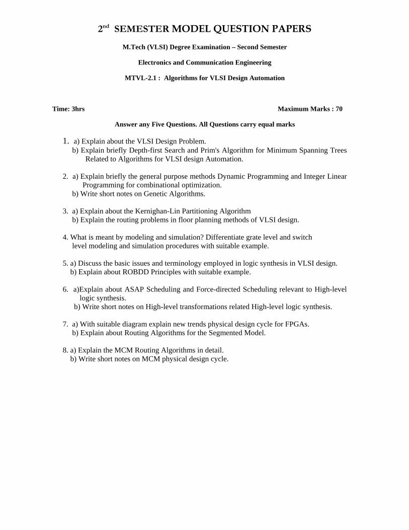
1. a) Explain about the VLSI Design Problem. b) Explain briefly Depth-first Search and Prim's Algorithm for Minimum Spanning Trees
Related to Algorithms for VLSI design Automation. 2. a) Explain briefly the general purpose methods Dynamic Programming and Integer Linear
Programming for combinational optimization. b) Write short notes on Genetic Algorithms. 3. a) Explain about the Kernighan-Lin Partitioning Algorithm b) Explain the routing problems in floor planning methods of VLSI design. 4. What is meant by modeling and simulation? Differentiate grate level and switch level modeling and simulation procedures with suitable example. 5. a) Discuss the basic issues and terminology employed in logic synthesis in VLSI design. b) Explain about ROBDD Principles with suitable example. 6. a)Explain about ASAP Scheduling and Force-directed Scheduling relevant to High-level
logic synthesis. b) Write short notes on High-level transformations related High-level logic synthesis. 7. a) With suitable diagram explain new trends physical design cycle for FPGAs. b) Explain about Routing Algorithms for the Segmented Model.
8. a) Explain the MCM Routing Algorithms in detail. b) Write short notes on MCM physical design cycle.
Model Question Paper
M.Tech (VLSI) Degree Examination – Second Semester
Electronics and Communication Engineering
MTVL-2.2: System Modelling and Simulation
Time: 3hrs Maximum Marks : 70
Answer any Five Questions. All Questions carry equal marks
1. (a) Define system modelling and simulation.
(b) Explain about discrete and distributed delays.
2. (a) Explain in detail system encapsulation.
(b) Compare different simulation packages with programming languages.
3. (a) Discuss about standard Petrinet nomenclatures.
(b) Explain alternative approach to modelling and simulation.
4. (a) Discuss about M/M/C queues.
(b) Define Poisson process? List out the Poisson postulates and its properties.
5. (a) Discuss about random walks and draw the state-diagram for a four-node random walk with reflecting borders.
(b) Explain system encapsulation.
6. (a) Explain in detail about alpha/Beta trackers.
(b) Discuss about multi-dimensional optimization.
7. (a) Explain in detail about continuous time Markov process.
(b) Explain about state machines.
8. (a) Discuss the techniques for increasing model validity and credibility.
(b) Explain about queuing theory and types of queues.
Model Question Paper
M.Tech (VLSI) Degree Examination – Second Semester
Electronics and Communication Engineering
MTVL-2.3 : CPLD AND FPGA Architecture and applications
Time: 3hrs Maximum Marks : 70
Answer any Five Questions. All Questions carry equal marks
1 . a) Distinguish between ROM’s, PLAs and PALS. b) Mention the features of Altera Flex logic-1000 series CPLD. 2. a) When is CPLD better suited than SPLD. b) Give the Design Flow for xilinx FPGA’s. 3. a) Give the routing architectures and logic Blocks of FPGA. b) Give the architecture and salient features of optimized Reconfigurable cell Array
(ORCA) of AT&T. 4. a) Why is it that PLDs are better than LCAs where the number of variables is large? b) Describe the Xilinx 4000 series FPGAs. 5. a) Explain about Linked state Machines and one-Hot state machine. b) Explain about the term Synchronization. Give its significance. 6. a) The reduced state table of a sequential machine has 12 rows. What is the minimum number of flip-flops needed to implement the machine? b) With an example explain about one Hot design Method using ASMs. 7. a) Explain about Linked State Machines. b) Explain the FSM architecture centered around shift registers. 8. Write notes on any TWO of the following. a) Mentor Graphics EDA tool b) ACTEL’s and their speed performance. c) Parallel adder design using FPGA.
Model Question Paper
M.Tech (VLSI) Degree Examination – Second Semester
Electronics and Communication Engineering
MTVL-2.4 : Low Power VLSI Design
Time: 3hrs Maximum Marks : 70
Answer any Five Questions. All Questions carry equal marks
1. a) What are the limitations of Low power designing? b) Draw the cross-section diagram of BiCMOS structure of an npn bipolar transistor is
added to a basic n-well CMOS process and explain it. 2. a) Draw the cross section of a transistor fabricated using the CDI process and explain
how Isolation is obtained. b) Prove that in BiCMOS process the operating voltage is limited by the BVCEO. 3. a) What is the need for copper in SOI BiCMOS? b) Draw the cross-sectional view of SOI lateral BJT and write its electrical characteristics. 4. a) What are the features of MOSFET in Noise model? b) What are the limitations of MOS Device models? c) How Device current can be extracted ? 5. a) Draw the Two input NAND gate using BiCMOS logic gates and explain its operation
with truth table. b) Draw the circuit diagram of BiCMOS buffer and explain its working. 6. a) Compare the conventional and advanced BiCMOS circuits. b) What is ESD? Design a ESD-free BiCMOS Inverter. 7. a) How to avoid feed through problems and race conditions in flip-flops? b) How pipe lining is used in C2MOS flip-flops? 8. a) Draw the circuit diagram of a CVSL style clocked SR latch with S and R as active high
inputs and explain it. b) Explain how the quality of Latches and flip-flops is measured
Model Question Paper
M.Tech (VLSI) Degree Examination – Second Semester
Electronics and Communication Engineering
ELECTIVE-III
MTVL-2.5(c) – CELLULAR AND MOBILE COMMUNICATIONS
Time: 3hrs Maximum Marks : 70
Answer any Five Questions. All Questions carry equal marks
1. Discuss sequence of steps in initiating a cell from one cell user to the others. 2. (a)What is meant by frequency reuse concept and what are the important points to be
considered in frequency reuse concept. (b) Discuss near field and far field problems in cellular systems. 3. Explain clearly forward and reverse channels for CDMA systems. 4. (a) Discuss clearly the important parameters of multipath channels. (b)Discuss important indoor propagation models. 5. Discuss important power control strategies used in mobile communications. 6.Discuss different methods to improve the capacity and coverage of existing cellular system. 7. (a) Discuss the advantages of space diversity antennas used at cell site. (b) Discuss different hand-off strategies. 8. Write short notes on the following. (a) Rake receiver (b) Personal mobile satellite communications (c) LEO
Model Question Paper
M.Tech (VLSI) Degree Examination – Second Semester
Electronics and Communication Engineering
ELECTIVE-IV
MTVL-2.6(a) – Microcontrollers and Embedded Systems
Time: 3hrs Maximum Marks : 70
Answer any Five Questions. All Questions carry equal marks
1. (a) List and define the three main characteristics of embedded systems that distinguish such systems from other computing system. (2)
(b) List and define the three IC technologies. What are the benefits of using each of the three different IC technologies. (4)
(c) What is a Single-Purpose Processor? Design a custom Single-Purpose Processor? Explain with an example. (8)
2. (a) Explain the software development process of an embedded system. (7)
(b) Enumerate the similarities and differences between a Microcontroller and Digital Signal Processor. (7)
3. (a) Given a 100MHz Crystal-Controlled Oscillator and a 32-bit and any number of 16-bit terminal counters. Design a relative clock that outputs the date and time down to milliseconds. You can ignore leap years. Draw a diagram and indicate terminal-count values for all counters. (9)
(b) A watchdog timer uses two cascaded 16-bit up-counters is connected to an 11.981MHz oscillator. A time out should occur if the function watchdog-reset is not called within 5 minutes. What value should be loaded into the up-counter pair when the function is called. (5)
4. (a) Explain the cache impact on system performance with an example. (7)
(b) Given the following three cache designs, find the one with best performance by calculating the average cost of access. Show all calculations.
i. 4 Kbyte, 8-way set-associative cache with a 6% miss rate cache hit costs one cycle, cache miss cost 12 cycles.
ii. 8 Kbyte, 4-way set-associative cache with a 4% miss rate cache hit costs two cycle, cache miss cost 12 cycles.
iii. 16 Kbyte, 2-way set-associative cache with a 2% miss rate cache hit costs three cycle, cache miss cost 12 cycles. (7)
5. (a) Draw the timing diagram for a bus protocol that is handshaked non-addressed and transfers 8-bits of data over a 4-bit data bus. (7)
(b) Explain the benefits an interrupt address table over fixed and vector interrupt methods. (7)
6. List the modifications made in Implementation: 2 (Microcontroller and CCDPP) and Implementation: 3 Microcontroller and CCDPP/ Fixed –Point DCT and discuss why each was beneficial in terms of performance. (14)
7. (a) Define the following terms: (7)
(i) Finite-state machines concurrent processor,
(ii) Real-time systems, and
(iii) Real-time operating systems.
(b) List three requirements of real-time systems and briefly describe each. Give examples of actual Real-time systems to support your arguments. (7)
8. Write notes on the following.
(a) Common Memory Types. (7)
(b) Stepper Motor Controllers. (7)