schottky diode graphene based sensors - intelligent...
TRANSCRIPT

Schottky Diode Graphene Based Sensors
A. Ashour, M. Saqr, M. AbdelKarim, A. Gamal, A. Sharaf
YJ-Science and Technology Research Center The American University in Cairo
New Cairo, Egypt
M. Serry Department of Mechanical Engineering
The American University in Cairo New Cairo, Egypt
Abstract—In this paper, we aim to demonstrate a novel scheme for integration of nanostructured semiconductor Graphene Oxide (GO) shottky diodes on flexible substrate for a wide range of sensing applications. The platform introduces a novel flexible GO/Pt/n-Si and GO/Pt/SiN composite structures which provides excellent optical and electrical properties, while maintaining an acceptable mechanical, biocompatibility, and return loss performance. The new structure was investigated for glucose, radiation, and infrared sensing. The sensors results showed ultrahigh sensitivity and high linearity in the targeted regions of interest. Moreover, the use of nanostructured materials allows for the development of a new generation of modern printed circuit antennas and will enable wide range of applications merging both technologies for a wide range of wearable and implantable sensing devices.
Keywords-graphene oxide; graphene; shottcky diode; radiation sensor; glucose sensing
I. INTRODUCTION This paper reports on new fabricated range of
sensors based on Schottky diode fabricated by depositing thin film semiconductor Graphene Oxide (GO) on platinum/silicon substrate. The unique nanostructure of the diode provides rapid and ultrahigh sensing capabilities for a wide range of sensing applications. A range of fabricated devices with different material and substrate properties are proposed for glucose sensing, thermal infrared, and gamma-ray (γ-ray) radiation sensing. This paper discusses the applications of this class of nanostructured Shottky diodes and presents the recent results in above proposed sensing applications.
Rapid and ultrahigh sensing of gamma-ray (γ-ray) radiation based on a new nanostructure GO grown on Platinum/n-type Silicon (Pt/n-Si) substrate which gives a Schottky rectifier response with different threshold voltages. The diodes were exposed to a range of γ-ray irradiations (5 − 35 KG) and a change in terminal voltages before and after radiation were measured accordingly. The
sensitivity was predicted to be (2 mA/KG) over a wide detection range, which is higher than the state-of-the-art radiation sensor devices. Moreover, the proposed sensor operates on low power, isotropic (i.e., independent of the radiation exposure angle), easy to fabricate, can operate wirelessly, and can be seamlessly integrated in wearable detection devices for ultrahigh sensitivity online monitoring of γ-ray radiations. We implemented a Schottky barrier selective gamma-photon sensitive nanostructure based on semiconductor GO electrodes on top of Pt/n-Si substrate (see Fig. 1). The nanostructured semiconductor GO electrodes result in high surface to volume ratio as compared to bulk capacitor electrodes, which consequently leads in increased sensitivity as a result of alterations in the Schottky rectifier threshold voltage as a result.
The proposed nanostructured diodes were also proposed for a new concept for wireless and passive sensor for continuous glucose monitoring that is based on SAW resonator coupled with glucose sensitive material based on semiconductor GO grown on thin film platinum grown on silicon substrate. Upon exposure to different glucose concentrations, electron is transferred from GO through the platinum substrate leading to change in the Insertion Loss (IL) of the output signal. It was found that the output signal can be correlated with high linearity to the glucose over a wide range of concentrations [0-25] mM the proposed system has several advantages over conventional ones, namely 1) wireless, 2) passive, 3) small size and its promising a replacement of bulky sensors in commercially available insulin pumps, creating more appropriate devices for treating diabetes.
The proposed nanostructure was also investigated as a new IR detection method which was proven to be good candidate to enhance the performance levels
Proceedings of the 8th International Conference on Sensing Technology, Sep. 2-4, 2014, Liverpool, UK
241

of micromachined uncooled infrared bolometer arrays and leads to a new technology trend.
II. GAMMA-RAY RADIATION SENSING
A. Motivation Detecting small doses of radiation in the
environment is critical for communities living close to nuclear plants or in the event of nuclear disasters, e.g., Fukushima (2011) and Chernobyl (1986). With more than 498 power reactors currently operating or under construction in 30 countries [1], accompanied by the unsolved problem of post-process storage of nuclear wastes and reliable controlling of potential environmentally induced leakages, there is an urgent need for relatively cheap and simple to used sensor of a wide range of radiation doses [2].
Nanostructured materials on MEMS integrated devices could replace most current conventional radiation sensors, the majority of which rely mainly on lattice defects in single crystal silicon structures that are induced by irradiation [3]. These defects are detected through resistance or capacitance changes. The current techniques, however, have substantial drawbacks: 1) limited sensitivity; 2) high probability of error; and 3) limited efficacy (i.e., one-time usage). Increasing surface to volume ratio and increasing material’s selectivity could potentially overcome the limited detection range and low sensitivity of conventional bulk capacitive radiation sensors.
Figure 1. SEM top-view showing semiconductor GO grown on top of Pt/n-Si substrate.
B. Results The samples were irradiated with γ-ray from
cobalt 60 (Co60), the IV characteristics for different
samples were measured using the 4156C high precision semiconductor parameter analyzer before and after irradiation. Fig. 2 shows the forward current versus input voltage characteristics for first sample both unexposed sample and exposed sample by 5 and 10 KG of the fabricated sensor. The sensor’s sensitivity represented by the curve in Fig. 3. The obtained results showed a functional radiation sensor operating with high efficiency over a wide detection range.
Figure 2. I-V characteristic for exposed samples with gamma photons with
doses from 2KG to 20KG in 2KG step (Device 1).
Figure 3. Sensitivity of the sensor as forward current change vs. dose rate.
III. GLUCOSE SENSING A novel technique for rapid and ultrahigh sensing
of glucose (i.e., blood sugar) based on a new nanostructure of semiconductor GO grown on platinum substrate and integrated with Surface Acoustic Wave (SAW) sensor. The origin of high
Proceedings of the 8th International Conference on Sensing Technology, Sep. 2-4, 2014, Liverpool, UK
242
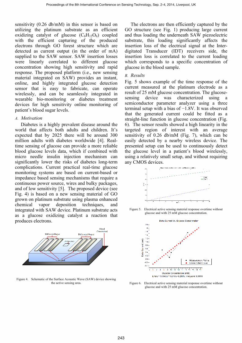
sensitivity (0.26 db/mM) in this sensor is based on utilizing the platinum substrate as an efficient oxidizing catalyst of glucose (C6H12O6) coupled with the efficient capturing of the produced electrons through GO forest structure which are detected as current output (in the order of mA) supplied to the SAW sensor. SAW insertion losses were linearly correlated to different glucose concentration showing high sensitivity and rapid response. The proposed platform (i.e., new sensing material integrated on SAW) provides an instant, online, and highly integrated glucose detection sensor that is easy to fabricate, can operate wirelessly, and can be seamlessly integrated in wearable bio-monitoring or diabetes treatment devices for high sensitivity online monitoring of patient’s blood sugar levels. A. Motivation
Diabetes is a highly prevalent disease around the world that affects both adults and children. It’s expected that by 2025 there will be around 300 million adults with diabetes worldwide [4]. Real-time sensing of glucose can provide a more reliable blood glucose levels data, which if combined with micro needle insulin injection mechanism can significantly lower the risks of diabetes long-term complications. Current practical real-time glucose monitoring systems are based on current-based or impedance based sensing mechanisms that require a continuous power source, wires and bulky packages, and of low sensitivity [5]. The proposed device (see Fig. 4) is based on a new sensing material of GO grown on platinum substrate using plasma enhanced chemical vapor deposition techniques, and integrated with SAW device. Platinum substrate acts as a glucose oxidizing catalyst a reaction that produces electrons.
Figure 4. Schematic of the Surface Acoustic Wave (SAW) device showing the active sensing area.
The electrons are then efficiently captured by the GO structure (see Fig. 1) producing large current and thus loading the underneath SAW piezoelectric substrate, this loading significantly affects the insertion loss of the electrical signal at the Inter-digitated Transducer (IDT) receivers side, the insertion loss is correlated to the current loading which corresponds to a specific concentration of glucose in the blood sample. B. Results Fig. 5 shows example of the time response of the current measured at the platinum electrode as a result of 25 mM glucose concentration. The glucose-sensing device was characterized using a semiconductor parameter analyzer using a three terminal setup with a bias of −1.8V. It was observed that the generated current could be fitted as a straight-line function in glucose concentration (Fig. 6). The sensor results showed a high linearity in the targeted region of interest with an average sensitivity of 0.26 db/mM (Fig. 7), which can be easily detected by a nearby wireless device. The presented setup can be used to continuously detect the glucose level in a patient’s blood wirelessly, using a relatively small setup, and without requiring any CMOS devices.
Figure 5. Electrical active sensing material response overtime without
glucose and with 25 mM glucose concentration.
Figure 6. Electrical active sensing material response overtime without glucose and with 25 mM glucose concentration.
Proceedings of the 8th International Conference on Sensing Technology, Sep. 2-4, 2014, Liverpool, UK
243

Figure 7. Device sensitivity (Insertion loss vs. Glucose Concentration).
IV. INFRARED SENSING The structure was also investigated for rapid and
low noise infrared (IR) detection. Micromachined thermal infrared detectors are gaining much attention in the recent years due to the rapid expansion in consumer electronics market. Therefore, it’s required to develop low-cost and CMOS integrated technology with minimal effects on performance levels [6]. Enhancing the infrared detectors’ performance is based on providing fast response (i.e., low thermal time constant), small pixel size, and broad detection band (i.e., in the 3−5 µm and 8−14 µm wavelength region), while maintaining low noise (i.e., low NEP, NETD, and Temperature fluctuation). Current technologies are based on developing the thermal infrared sensing material (e.g., amorphous silicon, silicon germanium, and vanadium oxide) and detection method (e.g., resistive, pyroelectric, and ferroelectric) [7]. Continuing on the same efforts, we investigate a new thermal infrared detection method based on GO nanostructure grown on platinum. The origin of high sensitivity is the large thermal conductance and low heat capacitance of GO thin film which leads to very small thermal time constant. Moreover, through the control of the nanostructure, it was possible to optimize the noise parameters (i.e., Noise Equivalent Power (NEP) (Fig. 8), Noise Equivalent Temperature Difference (NETD) (Fig. 9), and Temperature fluctuation) while maintaining high responsivity and detectivity.
V. CONCLUSIONS
This work demonstrated a novel scheme for integration of nanostructured semiconductor Graphene Oxide (GO) shottky diodes on flexible
substrate for a wide range of sensing applications. The sensing capabilities of the new structure were investigated for gamma-ray, glucose, and infrared sensing. The sensor demonstrated ultrahigh sensitivity and good linearity in the different ranges of interests. The new structure provides a new sensing technology trend.
Figure 8. Noise Equivalent Powre (NEP) versus number of walls at different
structure’s aspect ratio.
Figure 9. Noise Equivalent Temperature Difference (NETD) versus number of walls at different structure’s aspect ratio.
REFERENCES [1] International Atomic Energy Agency, Nuclear Security Report, 5
September, 2011. [2] B. K. Sovacool, A Critical Evaluation of Nuclear Power and Renewable
Electricity in Asia, J. of Contemporary Asia, 40 (2010) 379-380. [3] L. Wang, et al., Gamma and electron beam irradiation effects on the
resistance of micromachined polycrystalline silicon beams, Sensors and Actuators A, 177 (2012), 99–104.
[4] World Health Organization (WHO) Fact Sheet N°236. [5] N. S. Oliver et. al, “ Glucose sensors: a review of current and emerging
technology,” Diabetic Medicine, vol. 26, 2009, pp.197–210. [6] A. Schaufelbuhl et. al, “Uncooled low-cost thermal imager based on
micromachined CMOS integrated sensor array,” Journal of Microelectromech. Sys., vol. 10, 2001, pp.503–510.
[7] P. Muralt, “Micromachined infrared detectors based on pyroelectric thin films,” Reports on Progress in Physics, vol. 64, 2001, pp.1339–1388.
Proceedings of the 8th International Conference on Sensing Technology, Sep. 2-4, 2014, Liverpool, UK
244