scratchpad memories: a design alternative for cache on-chip memory in embedded systems
DESCRIPTION
Scratchpad Memories: A Design Alternative for Cache On-chip Memory in Embedded Systems. - Nalini Kumar Gaurav Chitroda Komal Kasat. OUTLINE. Introduction Scratch pad memory Cache memory Proposed methodology Results Conclusions. INTRODUCTION Scratch pad memory Cache memory - PowerPoint PPT PresentationTRANSCRIPT

SCRATCHPAD MEMORIES: A DESIGN ALTERNATIVE FOR CACHE ON-CHIP MEMORY IN EMBEDDED SYSTEMS
- Nalini Kumar
Gaurav Chitroda
Komal Kasat

2
Spring 2010, EEL 6935, E
mbedded System
s
OUTLINE Introduction Scratch pad memory Cache memory Proposed methodology Results Conclusions
04/09/2010
3
Spring 2010, EEL 6935, E
mbedded System
s
INTRODUCTION Scratch pad memory Cache memory Proposed methodology Results Conclusions
04/09/2010

4
Spring 2010, EEL 6935, E
mbedded System
s
INTRODUCTION Scratch pad memory:
A high speed internal memory used for temporary storage of calculations, data and other work in progress.
It is next closest memory to the ALU after the internal registers.
Scratch pad based systems have NUMA(Non-Uniform Memory Access) latencies, and use explicit instructions to move data. DMA based data transfer is often used.
On chip caches using SRAM consume power in the range of 25% to 45% of the total chip power
Current embedded processors for multimedia applications have on-chip scratch pad memories
04/09/2010
5
Spring 2010, EEL 6935, E
mbedded System
s
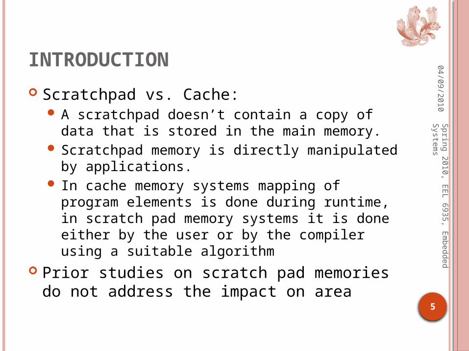
INTRODUCTION Scratchpad vs. Cache:
A scratchpad doesn’t contain a copy of data that is stored in the main memory.
Scratchpad memory is directly manipulated by applications.
In cache memory systems mapping of program elements is done during runtime, in scratch pad memory systems it is done either by the user or by the compiler using a suitable algorithm
Prior studies on scratch pad memories do not address the impact on area
04/09/2010

6
Spring 2010, EEL 6935, E
mbedded System
s
CONTRIBUTIONS The paper proposes scratchpad memory as an
alternative to cache memory as on-chip memory for computationally intensive applications.
CACTI tool is used for computing area and energy for AT91M40400 target architecture.
The results establish scratchpad memory as a low power alternative in most situations with an average energy reduction of 40%
04/09/2010

7
Spring 2010, EEL 6935, E
mbedded System
s
Introduction SCRATCH PAD MEMORY Cache memory Proposed methodology Results Conclusions
04/09/2010

Spring 2010, EEL 6935, E
mbedded System
s
8
SCRATCH PAD MEMORY 04/09/2010
Memory array with the decoding and the column circuitry logic
Memory objects are mapped to the scratch pad in the last stage of the compiler
It occupies one distant part of the memory address space. No need to check for data/instr. availability in the scratch pad
Reduces the comparator and the signal miss/hit acknowledging circuitry
Figure: Scratch Memory Array
6 Transistor Static RAM
Memory Array
Memory Cell

9
Spring 2010, EEL 6935, E
mbedded System
s
SCRATCH PAD MEMORY Area of scratchpad, As
As = Asde + Asda + Asco + Aspr + Asse + Asou
Energy Consumption is estimated from the energy consumption of the components
Escratchpad = Edecoder + Ememcol
Components: Data decoder, data array area, column multiplexers, pre charge circuit, data sense amplifiers, output driver circuitry
Memory array is the major consumer of energy CACTI tool first computes the capacitances for each
unit then estimates the energy
04/09/2010

10
Spring 2010, EEL 6935, E
mbedded System
s
ESTIMATING THE ENERGY CONSUMPTION For the memory array:
Ememcol = Cmemcol * Vdd2 * P0->1
Cmemcol is the capacitance of the memory array unit and is calculated as
Cmemcol = ncols * (Cpre + Creadwrite)
P0->1 is the probability of bit toggle, 0.5 Only two word lines are switched regardless of the
change in the address bits Total energy spent in the scratch pad memory is
Esptotal = SPaccess * E scratchpad
The only case that holds good is read or write access
04/09/2010
11
Spring 2010, EEL 6935, E
mbedded System
s
Introduction Scratch pad memory CACHE MEMORY Proposed methodology Results Conclusions
04/09/2010

Spring 2010, EEL 6935, E
mbedded System
s
12
CACHE MEMORY 04/09/2010
Area model is based on the transistor count in the circuitry
Area of the cache,Ac = Atag + Adata
where
Atag = Adt + Ata + Aco + Apr + Ase +
Acom + Amu and Adata = Ade + Ada + Acol + Apre + Asen + Aout
Figure: Cache Memory Organization
Tag Array Data Array
13
Spring 2010, EEL 6935, E
mbedded System
s
Introduction Scratch pad memory Cache memory PROPOSED METHODOLOGY Results Conclusions
04/09/2010
14
Spring 2010, EEL 6935, E
mbedded System
s
EXPERIMENTAL SETUP Compare same size cache with scratchpad memory
(the delay of cache is higher than scratchpad for the same technology)
Identification and Assignment of critical data structures to scratch pad in based on a packing algorithm
Total number of clock cycles determines the performance
Larger the number of clock cycles, lower the performance because on-chip configuration doesn’t change the clock period
04/09/2010

15
Spring 2010, EEL 6935, E
mbedded System
s
SCRATCH PAD MEMORY ACCESS Performance estimation from the trace file. An appropriate latency is added to the overall
program delay on scratchpad access: one for scratch pad read/write access, one cycle and one wait cycle for 16 bit main memory
access, one cycle plus three wait states for main memory 32 bit
access
04/09/2010
Access Number of Cycles
Cache Using Cache calculations
Scratch Pad 1 cycle
Main memory 16 bit 1 cycle + 1 wait cycle
Main memory 32 bit 1 cycle + 1 wait cycle

16
Spring 2010, EEL 6935, E
mbedded System
s
CACHE MEMORY ACCESS Authors assume a write through cache
Read Hit: Tag array is accessed. No write to cache and no access to main memory
Read Miss: One cache read operation, L (line size) words written to cache. One main memory read event of size L and no main memory write
Write Hit: Cache write followed by memory write Write Miss: One cache tag read and main memory write. No
cache update.
04/09/2010
Access type
Caread Cawrite Mmread Mmwrite
Read hit 1 0 0 0
Read miss 1 L L 0
Write hit 0 1 0 1
Write miss
1 0 0 1

17
Spring 2010, EEL 6935, E
mbedded System
s
C Benchmark
Mapping Algorithm
CACTI
Cache/Scratch Pad Size
Cache Number of
Cycles
Scratchpad Number of
cyclesTrace Analysis
Energy Aware Compiler
ARMulator trace analysis
FLOW DIAGRAM04/09/2010
Analytical model
Energy Estimates
Area Estimates
Compiler Support

18
Spring 2010, EEL 6935, E
mbedded System
s
EXPERIMENTAL SETUP Target architecture:
AT91M40400, based on embedded ARM 7TDMI embedded processor
High performance RSIC processor with a very low power consumption
On-chip scratch memory of 4KB. 32 bit data path and two instruction sets.
encc – energy aware complier, uses a special packing algorithm- knapsack algorithm for assigning code and data blocks to the scratch pad memory
The binary output of the compiler is simulated on the ARMulator to produce a trace file.
ARMulator accepts the cache size as a parameter for on-chip cache configuration and generates the performance as number of cycles.
The area and performance estimates are made for the 0.5um technology
04/09/2010

19
Spring 2010, EEL 6935, E
mbedded System
s
Introduction Scratch pad memory Cache memory Proposed methodology RESULTS Conclusions
04/09/2010

20
Spring 2010, EEL 6935, E
mbedded System
s
RESULTS 04/09/2010
Cache per access(2kB) 4.57 nJ
Scratch pad per access(2kB) 1.53 nJ
Main memory read access, 2 bytes 24.00 nJ
Main memory read access, 4 bytes 49.30 nJ
Main memory write access, 4 bytes 41.10 nJ
Size Bytes Area Cache
Area Scratchpad
CPU cycles Cache
CPU cycles, Scratchpad
Area reduction
Time reduction
Area-time product
64 6744 4032 481.9 347.5 0.40 0.28 0.44
128 11238 7104 302.4 239.9 0.37 0.21 0.51
256 21586 14306 264.0 237.9 0.34 0.10 0.55
512 38630 26722 242.6 237.9 0.31 0.10 0.61
1024 74680 53444 241.7 192.0 0.28 0.21 0.55
2048 142224 102852 241.5 192.0 0.28 0.20 0.57
Average 0.33 0.18 0.54
Table: Energy per access of various devices
Table: Area/Performance ratios for bubble-sort
The average area, time and AT product reductions are 34% 18% and 46%

Spring 2010, EEL 6935, E
mbedded System
s
21
RESULTS 04/09/2010
Figure: Energy consumed by the memory system
Figure: Comparison of cache and scratch pad memory area
22
Spring 2010, EEL 6935, E
mbedded System
s
Introduction Scratch pad memory Cache memory Proposed methodology Results CONCLUSION
04/09/2010

23
Spring 2010, EEL 6935, E
mbedded System
s
CONCLUSION Presents an approach for selection of on-chip memory
configurations Results show that scratch pad based compile time
memory outperforms cache-based run-time memory on almost counts.
40% average reduction for the application considered Authors propose study of DRAM based memory
comparisons since memory bandwidth and on-chip memory capacity are limiting factors for many applications.
Also, the energy models for both cache and scratchpad need to be validated by real measurements
04/09/2010

24
Spring 2010, EEL 6935, E
mbedded System
s
QUESTIONS
04/09/2010