scte ips template, rev 3 196 2013.pdf · 6.2.3 sfp-rf module control sequence ... 8.2 sfp-rf module...
TRANSCRIPT

ENGINEERING COMMITTEE Interface Practices Subcommittee
SCTE 196 2013
SFP-RF: Interface Specifications for an RF-Modulated
Small Form Factor Pluggable Optical Module

i
NOTICE
The Society of Cable Telecommunications Engineers (SCTE) Standards are intended to serve the public interest by providing specifications, test methods and procedures that promote uniformity of product, interchangeability and ultimately the long term reliability of broadband communications facilities. These documents shall not in any way preclude any member or non-member of SCTE from manufacturing or selling products not conforming to such documents, nor shall the existence of such standards preclude their voluntary use by those other than SCTE members, whether used domestically or internationally.
SCTE assumes no obligations or liability whatsoever to any party who may adopt the Standards. Such adopting party assumes all risks associated with adoption of these Standards, and accepts full responsibility for any damage and/or claims arising from the adoption of such Standards.
Attention is called to the possibility that implementation of this standard may require the use of subject matter covered by patent rights. By publication of this standard, no position is taken with respect to the existence or validity of any patent rights in connection therewith. SCTE shall not be responsible for identifying patents for which a license may be required or for conducting inquiries into the legal validity or scope of those patents that are brought to its attention.
Patent holders who believe that they hold patents which are essential to the implementation of this standard have been requested to provide information about those patents and any related licensing terms and conditions. Any such declarations made before or after publication of this document are available on the SCTE web site at http://www.scte.org.
All Rights Reserved
© Society of Cable Telecommunications Engineers, Inc. 2013
140 Philips Road Exton, PA 19341

ii
TABLE OF CONTENTS
1.0 SCOPE .........................................................................................................1
2.0 NORMATIVE REFERENCES ...................................................................1
3.0 INFORMATIVE REFERENCES ................................................................2
3.1 SCTE Standards and Specifications .................................................................. 2
3.2 Standards and Specifications from other Organizations ................................... 3
4.0 COMPLIANCE NOTATION ......................................................................3
5.0 DEFINITIONS, ABBREVIATIONS, AND ACRONYMS ........................3
6.0 MANAGEMENT INTERFACE ..................................................................4
6.1 Summary of 2-Wire Communications Requirements ....................................... 4
6.2 Theory of Operation .......................................................................................... 5
6.2.1 SFP-RF Module Boot-Up Sequence ................................................................. 5
6.2.2 Host Initialization of the SFP-RF Module ........................................................ 8
6.2.3 SFP-RF Module Control Sequence ................................................................. 10
6.2.4 SFP-RF Module Not Ready ............................................................................ 13
6.2.5 Interrupt Conditions from the SFP-RF Module .............................................. 13
6.3 SFP-RF Module Memory Map ....................................................................... 14
6.4 Specific Memory Maps ................................................................................... 17
6.4.1 Volatile and Non-Volatile Field Characteristics ............................................. 17
6.4.2 Lower Memory Map (Common Table) .......................................................... 17
6.4.3 Upper Memory Maps ...................................................................................... 18
7.0 ELECTRICAL INTERFACE ....................................................................27
7.1 Introduction ..................................................................................................... 27
7.2 Pinout .............................................................................................................. 28
7.2.1 Pin Definitions ................................................................................................ 30

iii
7.3 Fixed Forward RF Input .................................................................................. 33
7.3.1 Pass Band ........................................................................................................ 35
7.3.2 RF Power Levels ............................................................................................. 35
7.3.3 Interface Impedance ........................................................................................ 37
7.3.4 Input Return Loss ............................................................................................ 37
7.3.5 Amplitude Balance for Differential RF Input ................................................. 37
7.3.6 Phase Balance for Differential Input ............................................................... 38
7.4 DC Power Requirements ................................................................................. 38
7.4.1 Power Noise Output ........................................................................................ 38
7.4.2 SFP-RF Module Power Noise Susceptibility .................................................. 39
7.5 Low Speed Electrical Specifications............................................................... 39
7.6 Timing Requirements of Control and Status I/O ............................................ 40
7.7 Wavelength and Power Protection during Startup for DWDM SFP-RF Modules ...................................................................................................................... 41
7.7.1 Cold Start ........................................................................................................ 43
7.7.2 Laser Start (Tx On) ......................................................................................... 43
7.7.3 Laser Shutdown .............................................................................................. 43
7.7.4 Power Supply Shutdown ................................................................................. 43
7.7.5 Protection Condition ....................................................................................... 43
8.0 MECHANICAL AND BOARD DEFINITION.........................................44
8.1 Introduction ..................................................................................................... 44
8.2 SFP-RF Module Mechanical and Labeling Requirements .............................. 44
8.3 Mating of SFP-RF Module PCB to the Host Electrical Connector ................ 44
8.4 Host Board Layout .......................................................................................... 45
8.5 Insertion, Extraction and Retention Forces for SFP-RF Modules .................. 45
8.6 Color Coding of SFP-RF Modules.................................................................. 45

iv
8.7 EMI Design Using SFP-RF Modules.............................................................. 45
8.8 SFP-RF Module Connector Specifications ..................................................... 45
8.9 SFP-RF Module Cage Assembly Dimensions ................................................ 45
8.10 SFP-RF Module Cooling ................................................................................ 46
8.11 Environmental and Thermal............................................................................ 46
8.12 Dust Cover ...................................................................................................... 46
8.13 SFP-RF Module Fiber-Optic End-Face Finish and Connector Geometry ...... 46
APPENDIX A: POWER DIFFERENCES DUE TO NUMBER OF ACTIVE CHANNELS FOR DRFI-COMPLIANT HOSTS .................................................46
APPENDIX B: EXAMPLE POWER CHANGES INTO THE MODULE AS A FUNCTION OF THE NUMBER OF ACTIVE CHANNELS ..............................54
ACKNOWLEDGEMENTS ...................................................................................56
v
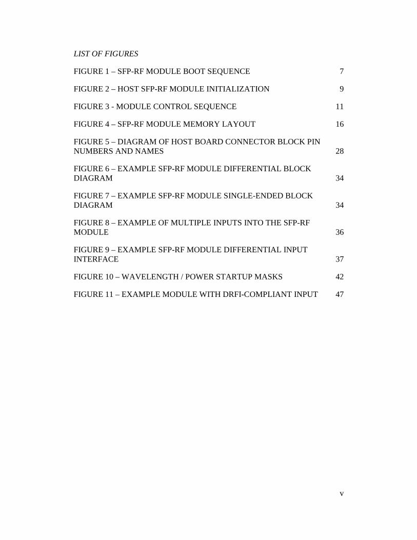
LIST OF FIGURES
FIGURE 1 – SFP-RF MODULE BOOT SEQUENCE 7
FIGURE 2 – HOST SFP-RF MODULE INITIALIZATION 9
FIGURE 3 - MODULE CONTROL SEQUENCE 11
FIGURE 4 – SFP-RF MODULE MEMORY LAYOUT 16
FIGURE 5 – DIAGRAM OF HOST BOARD CONNECTOR BLOCK PIN NUMBERS AND NAMES 28
FIGURE 6 – EXAMPLE SFP-RF MODULE DIFFERENTIAL BLOCK DIAGRAM 34
FIGURE 7 – EXAMPLE SFP-RF MODULE SINGLE-ENDED BLOCK DIAGRAM 34
FIGURE 8 – EXAMPLE OF MULTIPLE INPUTS INTO THE SFP-RF MODULE 36
FIGURE 9 – EXAMPLE SFP-RF MODULE DIFFERENTIAL INPUT INTERFACE 37
FIGURE 10 – WAVELENGTH / POWER STARTUP MASKS 42
FIGURE 11 – EXAMPLE MODULE WITH DRFI-COMPLIANT INPUT 47

vi
LIST OF TABLES
TABLE 1 – MAXIMUM CURRENT FIELDS 19
TABLE 2 – AUXILIARY INPUT TYPES 19
TABLE 3 – TABLE 70H READ ONLY VALUES 22
TABLE 4 – TABLE 70H WRITABLE VALUES 25
TABLE 5 – SFP MODULE ELECTRICAL PIN DEFINITION 28
TABLE 6 – COMMANDED STEP SIZE AND STEP SIZE ACCURACY 36
TABLE 7 – EXAMPLE POWER LEVELS AND STEP SIZES 36
TABLE 8 – POWER PER RAIL 38
TABLE 9 - LOW SPEED CONTROL AND SENSE SIGNALS, ELECTRONIC CHARACTERISTICS 40
TABLE 10 - TIMING PARAMETERS FOR SFP-RF MANAGEMENT 40
TABLE 11 – NUMBER OF CHANNELS IMPACT ON POWER PER CHANNEL 48
TABLE 12 – DRFI OUTPUT COMPOSITE POWER COMPARISON 49
TABLE 13 – COMPOSITE POWER WHEN PMAX = 3 DBM 54
TABLE 14 – COMPOSITE POWER WHEN PMAX = 6 DBM 55

1
1.0 SCOPE
The standardization and deployment of optical interfaces for headend equipment offer cost and power savings to MSOs. However, implementing optical interfaces in these devices presents significant technical challenges, since the lack of standardization may result in too many combinations of interfaces to support effectively in a headend device (power, wavelengths, cards, etc.).
Because of this challenge, the following specification proposes a standard for the interfaces between a downstream laser transmitter module and its host. The module is based on the [SFF-8431], but the input will consist of RF-modulated signals that will be amplitude modulated onto an optical carrier. For the purpose of this specification, this module is referred to as SFP-RF. This SFP-RF optical transmitter module could be integrated into headend equipment, such as a Converged Cable Access Platform (CCAP), a Cable Modem Termination System (CMTS), an Edge QAM, or a forward optical transmitter shelf, reducing the need for devices dedicated to forward lasers. The SFP-RF optical transmitter module will function as a downstream laser for the output of cable edge devices. The primary difference between the SFP-RF optical transmitter module and the XFP-RF optical transmitter module is the size of the module and the link lengths supported.
This standard will focus on the communications, electrical, and mechanical interfaces for the SFP-RF optical transmitter module. Unless otherwise noted, requirements held within this standard apply both to the transmitter module and its host.
2.0 NORMATIVE REFERENCES
The following documents contain provisions, which, through reference in this text, constitute provisions of the standard. At the time of Subcommittee approval, the editions indicated were valid. All standards are subject to revision; and while parties to any agreement based on this standard are encouraged to investigate the possibility of applying the most recent editions of the documents listed below, they are reminded that newer editions of those documents may not be compatible with the referenced version. Reference Description [IEC 61755-3-1] IEC 61755-3-1:2006, ed. 1.0, July 1, 2006, Fibre optic connector
optical interfaces – Part 3-1: Optical interface, 2,5 mm and 1,25 mm diameter cylindrical full zirconia PC ferrule, single mode fibre. IEC Sub-committee 86B
[IEC 61755-3-2] IEC 61755-3-2, ed. 1.0, July 12, 2006, Fibre optic connector optical interfaces - Part 3-2: Optical interface, 2,5 mm and 1,25 mm diameter cylindrical full zirconia ferrules for 8 degrees

2
angled-PC single mode fibres, IEC Sub-committee 86B [FINISH] IEC 61300-3-35, ed. 1.0, November 20, 2009, Fibre optic
interconnecting devices and passive components - Basic test and measurement procedures - Part 3-35: Examinations and measurements - Fibre optic connector endface visual and automated inspection, IEC Sub-committee 86B
[INF-8074] INF-8074i, Revision 1.0, May 12, 2001, Specification for SFP (Small Formfactor Pluggable) Transceiver, SFF Committee, http://www.sffcommittee.com/
[XFP MSA] INF-8077i, Revision 4.5, August 31, 2005, 10 Gigabit Small Form Factor Pluggable Module, SFF Committee, http://www.sffcommittee.com/
[SFF-8083] SFF-8083, Revision 2.5, January 19, 2010, 0.8mm Card Edge Connector for 8/10 Gb/s Applications, SFF Committee, http://www.sffcommittee.com/
[SFF-8431] SFF-8431, Revision 4.1, July 6, 2009, Enhanced Small Form Pluggable Module SFP+, SFF Committee, http://www.sffcommittee.com/
[SFF-8432] SFF-8432, Revision 5.0, July 16, 2007, Improved Pluggable Formfactor, SFF Committee, http://www.sffcommittee.com/
[SFF-8433] SFF-8433, Revision 0.7, June 5, 2009, Improved Pluggable Formfactor (IPF) for SFP+ Ganged Cages, SFF Committee, http://www.sffcommittee.com/
[SFF-8477] SFF-8477, Revision 1.4, December 4, 2009, Tunable XFP for ITU Frequency Grid Applications, SFF Committee, http://www.sffcommittee.com/
3.0 INFORMATIVE REFERENCES
The following documents may provide valuable information to the reader but are not required when complying with this specification.
3.1 SCTE Standards and Specifications Reference Description [DRFI] ANSI/SCTE 133 2010 Downstream RF Interface for Cable Modem
Termination Systems [SCTE 55-1] ANSI/SCTE 55-1 2009 Digital Broadband Delivery System: Out of
Band Transport Part 1: Mode A [SCTE 55-2] ANSI/SCTE 55-2 2008 Digital Broadband Delivery System: Out of
Band Transport Part 2: Mode B

3
3.2 Standards and Specifications from other Organizations Reference Description [UM10204] UM10204, Version 4.0, February 13 2012, The I2C-Bus
specification and user manual, NXP Semiconductors
4.0 COMPLIANCE NOTATION “SHALL” This word or the adjective “REQUIRED” means that the item is an
absolute requirement of this specification. “SHALL NOT” This phrase means that the item is an absolute prohibition of this
specification. “SHOULD” This word or the adjective “RECOMMENDED” means that there may
exist valid reasons in particular circumstances to ignore this item, but the full implications should be understood and the case carefully weighted before choosing a different course.
“SHOULD NOT” This phrase means that there may exist valid reasons in particular circumstances when the listed behavior is acceptable or even useful, but the full implications should be understood and the case carefully weighed before implementing any behavior described with this label.
“MAY” This word or the adjective “OPTIONAL” means that this item is truly optional. One vendor may choose to include the item because a particular marketplace requires it or because it enhances the product, for example; another vendor may omit the same item.
5.0 DEFINITIONS, ABBREVIATIONS, AND ACRONYMS Term Definition ADC Analog-to-Digital Converter AGC Automatic Gain Control APC Angled Physical Contact APD Avalanche Photodiode balun A device or component that provides a transition between a
balanced transmission line, circuit, source, or load, and an unbalanced transmission line, circuit, source, or load.
CLEI Common Language Equipment Identification EEPROM Electrically Erasable Programmable Read-Only Memory host The device into which the optical module is integrated. I/O Input/Output I2C Inter-Integrated Circuit, a 2-wire communication interface ITU International Telecommunication Union NVRAM Non-Volatile Random-Access Memory Pmax Maximum Composite Power Pref Reference composite power level that produces the optimal
performance of the SFP-RF module R/W Read/Write RF Radio Frequency

4
Term Definition RX Receive SCL Serial Clock SDA Serial Data SFP Small Formfactor Pluggable SFP-RF Downstream optical transmitter module, based on the SFP and
SFP-Plus MSAs, that transmits RF-modulated signals. SNR Signal-to-Noise Ratio TEC Thermo-Electric Cooler TX Transmit UPC Ultra Physical Contact XFP 10 Gigabit Small Form Factor Pluggable; a standard for an optical
transceiver. See [XFP MSA]. XFP-RF Downstream optical transmitter module, based on the XFP MSA,
that transmits RF-modulated signals.
6.0 MANAGEMENT INTERFACE
2-Wire Communications (I2C) for the SFP-RF module are based upon [XFP MSA]. I²C is an implementation of the NXP (formerly Philips) I²C [UM10204] specification with mapped memory address locations (also known as “well-known addresses”) for diagnostics and operations. The SFF Committee specifies the I²C common memory mapping in [XFP MSA] and [SFF-8477] for SFP and XFP, as well as additional physical layer requirements. This specification uses the same well-known memory map locations (addresses) for functions that are the same or substantially similar. Because the SFP-RF is a RF transmitter (and not a digital transceiver), some memory map fields from [XFP MSA] and [SFF-8477] are re-allocated or not used; in addition, some memory map fields have been added.
The SFP-RF module shall implement the I2C requirements specified in [XFP MSA], except where specified differently in the following sections.
6.1 Summary of 2-Wire Communications Requirements
In [XFP MSA] 2-wire communication requirements are spread across several sections, including Section 4.2 and Table 26, Section 2.6 and Table 3. The following bullets summarize these requirements; refer to [XFP MSA] for complete details.
• I²C communications may not be available for up to 300 ms after power up or reset
• The Mod_DeSel Pin functions as defined in section 4.2 of [XFP MSA]. Note, if the I²C interface bus is not shared, the Mod_DeSel Pin

5
may be pulled low permanently. Note that such a “chip select” pin is new to the SFP-RF and was not included in the [SFF-8431].
• There must be at least 20 µs between the STOP signal and the next START signal for a particular module.
• The clock rate can be as high as 400 kHz (I²C fast mode).
• Up to two START signals per command are allowed (the second START is also known as a RESTART signal).
• Only one STOP signal is allowed per command.
• Multiple master systems are not supported.
• Host boards shall accommodate SFP-RF modules which hold the SCL line low (clock stretching) for up to a maximum of 500 µs during an I²C read or write operation.
• After a write from the host to the module, the module may not respond to further I²C commands for up to 40 ms (typically this would be for writing non-volatile values). The phrase “not respond” means that the device address given immediately after the START signal from the host is not acknowledged by the module.
• I²C packet error checking protocol is optional as defined in the [XFP MSA].
6.2 Theory of Operation
The operations of the SFP-RF module are based on Chapter 5: Management Interface of [XFP MSA]. The following sections define the operation of the SFP-RF module I²C interface that is used for serial ID, digital diagnostics and other control/monitoring functions.
6.2.1 SFP-RF Module Boot-Up Sequence
When a SFP-RF module is plugged in, the host needs to perform a number of initialization steps in a particular order with a particular timing. Some of these involve the SFP-RF module pins, including the RF input, and some involve I²C communications. As most of these are documented in the [XFP MSA] or are implied by stated dependencies, a reference to the location(s) in that document will accompany each step in the following sequence descriptions.

6
Before the boot-up sequence can be discussed, communications and host requirements need to be understood.
6.2.1.1 I²C Communications Requirements
Once I²C is operational, the host shall adhere to the following timing and pin requirements (see [XFP MSA] Section 4.2, Table 26):
• The host shall pull Mod_DeSel low for a minimum of 2 ms before issuing the START signal (Host_select_setup).
• While Mod_DeSel is low, the host shall wait at least 20 µs after the previous STOP signal before issuing a new START signal (tBUF).
If the SFP-RF module is not sharing the I²C interface bus with other SFP-RF modules, the Mod_DeSel pin may be left low indefinitely. Otherwise, it shall be pulled high for at least 2 ms before another command is executed on the shared bus (presumably to a different SFP-RF module).
Write operations may cause the SFP-RF module to not respond to further I²C signals or messages for up to 40 ms (tWR in Section 4.3, Table 27, and Section 4.5.7 of [XFP MSA]). The specification does not restrict this to EEPROM writes. This applies for writes from one to four bytes (the limit for a write is four bytes).
The SFP-RF module may perform a clock stretch of up to 500 µs during read or write operations (T_clock_hold, [XFP MSA] Section 4.3, Table 27). This is distinct from unresponsiveness after a write operation (tWR).
6.2.1.2 Pin State Prior to SFP-RF Module Boot Up
Before a SFP-RF module can begin boot up, the host shall meet the following pin requirements.
The voltages listed for pins 12 (VEE5), 15 (VCC3_DIGITAL), and 16 (VCC3_ANALOG) in Table 5 – SFP Module Electrical Pin Definition shall be available.
The value of pin 7 (P_Down/RST) should be set to low to allow the SFP-RF module to run in full power (power level 2), although a setting of high may be used to limit the SFP-RF module to low power consumption (≤ 1.0 watts).

7
Refer to section 2.4.7.3, Module Behavior During Power Down and Reset of [XFP MSA] for further details.
Pin 8 (Interrupt) shall be pulled high by the host. If an unmasked error, alarm or warning condition is encountered during operation, the SFP-RF module shall pull this value low.
6.2.1.3 Initial SFP-RF Module Boot Sequence
Once the SFP-RF module is inserted, it goes through its initialization sequence, as shown in the following flow chart.
Figure 1 – SFP-RF Module Boot Sequence
This series of actions is described here.
1. The SFP-RF module shall indicate its presence to the host by grounding pin 6 (Mod_Abs) upon insertion.
2. After 300 ms, SFP-RF module initialization (aka Reset Complete, described in Section 2.4.7.3, Table 39 of [XFP MSA]) shall be finished (t_init, [XFP MSA] Section 2.6, Table 3).

8
3. The SFP-RF module shall assert pin 8 (Interrupt ) to low and set corresponding Reset Complete flag ([XFP MSA] Section 2.4.7.3, Table 39). Reset Complete can be detected by the host via an Interrupt signal (pin 8 pulled low) with a corresponding Reset Complete flag being set.
Note that until the boot sequence is complete, pin signals may not be valid and the SFP-RF module shall not assert the Interrupt pin spuriously, as detailed in Section 2.4.7.3 of [XFP MSA].
Note that completing these steps does not imply that the SFP-RF transmitter module is ready—the Mod_NR pin is a better indicator of that condition. The Reset Complete flag also does not imply that registers are valid; the module sets the Data_Not_Ready flag (from Table 42 in [XFP MSA]) to low to indicate that register contents are valid and can be read.
6.2.2 Host Initialization of the SFP-RF Module
After completion of the SFP-RF module boot sequence, the host shall initialize the module, including interrupt masks, RF control, and miscellaneous parameters, as detailed in the following flow chart.

9
Figure 2 – Host SFP-RF Module Initialization
This series of actions is described here.
1. The host can set alarm and warning masks for any events of interest. These can be found in Table 40 in Section 5.11.1 of [XFP MSA] with the exception of those alarms and warnings listed in section 7.4.2, Lower Memory Map (Common Table). By default none of these is masked. In particular, the Reset Complete status bit (and its corresponding Interrupt ) is not masked. At a minimum, the host should set the masking bits for:
• Receiver values (RX Power, RX_NR Status, RX_LOS, RX CDR Loss of Lock)

10
• APD Supply (which is not supported)
• Wavelength Unlocked
2. The host can clear any existing latched alarms by reading those alarm bits (the alarm bits are listed in Table 39 in Section 5.11.1 of [XFP MSA]). As these flags are latched, their initial presence does not necessarily indicate a continuing fault. For example, the presence of the Reset Complete flag upon insertion of the module is not a fault. During initialization the SFP-RF module may not have set the TX Bias and TX Power before testing for errors. Among those that can be reasonably expected are:
• TX_NR Status
• Receiver values as listed above
• Reset Complete
• Wavelength Unlocked
• TX Bias Low
• TX Power Low
3. In Table 70h in upper memory, the host should update the Link Length field. This is a non-volatile field.
4. In Table 70h in upper memory, the host shall set the RF Input Initialization Complete flag to false. Once all RF input level tweaking is done, this flag shall be set to true by the host, whereupon the SFP-RF module can make any further internal adjustments that may have interfered with the host or taken a long time.
Table 70h is a new table described in section 7.4.3.3 of this document.
6.2.3 SFP-RF Module Control Sequence
Once the boot-up sequence is complete and the module has indicated that it is ready, or when the host needs to change the RF input level (e.g. to add channels), the host and module exchange information through a series of read and write actions to the module’s non-volatile and volatile memory, as shown in Figure 3. These actions are written from the host’s point of view.

11
Figure 3 - Module Control Sequence

12
This series of actions by the host is described here. Note that if the RF level is being changed while the module is in operation, the flow begins at step 2.
1. After boot up, the host shall wait for the SFP-RF module power-up or reset initialization (at least 300 ms).
2. The host shall read the Pref value from the SFP-RF module. This value reflects the RF power level required for optimal performance.
3. The host shall write false to RF Input Initialization Complete in the SFP-RF module.
4. Using the Pref value, as well as other values known to the host (such as channel plan, RF offset, etc.), the host calculates RF level to apply. The resulting RF level could be lower than the reference value if the host is not providing the full range of channels to the SFP-RF module.
5. The host shall write the RF level to the RF Input Applied from Host field. At the same time, the host shall apply RF at the module input.
At this point, there is the potential for tighter control in a loop. This makes sense only if the SFP-RF module has a power meter as indicated by the Power Meter Measurement Interval being a value other than 0 (zero). However running the loop is harmless even without a power meter; this can simplify control logic in the host.
6. Host shall pause to allow time for the SFP-RF module to update the RF Input Measured from Module field. This pause shall be at least the duration in the Power Meter Measurement Interval field or 100 ms, whichever is greater. Additional delay may be inserted to reduce dithering or network traffic.
7. Host shall read the RF Input Measured from Module field and decide if an adjustment is required. If there is a power meter in the SFP-RF module, its calibration may differ from the host and hysteresis should enter into the decision.
8. If an adjustment is required, the host shall go to step 4 and re-calculate the RF needed, write that value to RF Input Applied from Host and apply RF to the SFP-RF module. Otherwise, the host shall write true to RF Input Initialization Complete and exit the loop.

13
The SFP-RF module detects write events to its memory; this allows the SFP-RF module to know when the host has changed the input RF level.
Implicit in this flow is the assumption that the SFP-RF module will not implement Automatic Gain Control (AGC), as it cannot know the current and future channel plans or other loading details. The host may choose to implement AGC by applying different RF inputs (and indicating those values via the RF Input Applied by Host field). That value may be used by the SFP-RF module for non-AGC purposes.
6.2.4 SFP-RF Module Not Ready
When an SFP-RF module is removed or a fatal condition is encountered, the Mod_NR pin (pin 2) is pulled high. When Mod_NR pin is high, it is recommended that the host mute the RF applied to the module to prevent any spurious emissions.
6.2.5 Interrupt Conditions from the SFP-RF Module
The following section is based on Section 5.11 of [XFP MSA]; modifications have been made for this specification.
The SFP-RF module shall implement a real-time hardware Interrupt pin (pin 8) to alert the host system to any condition outside normal operating conditions. Interrupt system logic shall be triggered and latched by a set of flags. These include:
• Alarm and warning flags as described in section 5.6, Basic Monitoring Functions of [XFP MSA]. These correspond to monitored quantities going outside factory programmed threshold values.
• Flags corresponding to basic SFP-RF module status conditions including:
• TX_NR: Any condition leading to invalid data on the TX path
• TX_Fault: Laser fault condition
• MOD_NR: Module Not Ready (mirroring hardware output pin)

14
• Reset Complete: Indicates completion of the SFP-RF Module Reset (as initiated by power up or P_Down/RST pin)
• Flags corresponding to optional extended capabilities including TEC Fault.
This specification uses byte 85, bit 0 for a vendor-specific alarm.
Nothing in the SFP-RF Table 70h is designed to produce an interrupt.
Existence of any of these conditions shall lead to a latched flag. These flags are located in bytes 80 – 87 and are detailed in Table 39 of [XFP MSA]. The presence of any 1 value in bytes 80 – 87 without a corresponding mask bit set to 1 will assert the hardware Interrupt output pin (active low). When the Interrupt pin alerts the host system to a latched flag condition, the host may query the latched flag bits in bytes 80 – 87. The SFP-RF module shall clear the latched flags upon the read of the corresponding latched flag bit.
Masking bits shall be volatile and startup with all unmasked (masking bits 0).
Hardware Interrupt Pin = Logical NOR of all (Latched Flag Bit AND NOT Masking Bit)
The mask bits can be used to prevent continued interruption from ongoing conditions. This specification uses byte 93, bit 0 for the vendor-specific alarm mask.
6.3 SFP-RF Module Memory Map
The structure of the SFP-RF module memory map is shown in Figure 4. The SFP-RF module shall implement the memory map specified in section 5 of [XFP MSA] and section 4 of [SFF-8477], with the exceptions specified here.
The normal 256 byte I²C address is divided into lower and upper blocks of 128 bytes. The lower block of 128 bytes is always directly available and is intended to be used for diagnostic and control functions that are accessed often. This is the common table; it is accessed if the I²C address is less than 128 without regard to the selected table.

15
Multiple blocks of memory are available in the upper 128 bytes of the address space. These are individually addressed via a table select byte located in the lower address space (at offset 127). The upper address tables are intended to contain information that is accessed less frequently, such as serial ID, user writable EEPROM, etc. The password must be entered before any upper memory can be accessed. The password entry stays in effect until the module is power cycled.
The I²C address of the SFP-RF module shall be 1010000Xb (A0h). In order to support access to multiple SFP-RF modules on the same I²C serial bus, the SFP-RF pin-out includes a Mod_Desel or module deselect pin. This pin shall be held low by the host to address a particular SFP-RF module.
Mod_NR (pin 2 per Table 5) shall include temperature stabilization of wavelength, upon start-up. That is, “Module Not Ready” includes the condition of a cooled laser not yet at the correct temperature. Laser temperature stabilization time should be on the order of several tens of seconds.
Figure 4 summarizes the memory layout. The major difference from [XFP MSA] is that a new table, 70h, is defined near the end of the range of the vendor-specific tables. Some fields are not supported, as detailed in section 7.4.2.

16
Figure 4 – SFP-RF Module Memory Layout
17
6.4 Specific Memory Maps
6.4.1 Volatile and Non-Volatile Field Characteristics
6.4.1.1 Non-Volatile Field Resilience
The SFP-RF module shall meet the [XFP MSA] specification requirement for EEPROM write cycles (at least 50,000 write cycles). If a host were to write to such a field once per minute, then the EEPROM would expire in roughly 35 days. Writing once per hour gives a lifetime of about 5.7 years.
6.4.1.2 Access Rate for Volatile and Read-Only Fields
While there is no maximum rate for these fields, there is an I²C limitation. Therefore, the host should not expect “tight loop” level of control.
6.4.2 Lower Memory Map (Common Table)
The lower 128 bytes of the I²C serial bus address space is used to access a variety of measurements and diagnostic functions, and to implement a set of control functions. The contents of the lower memory map shall conform to the [XFP MSA] I²C specification unless specified otherwise below.
• The following values are not used by the SFP-RF module. They are not repurposed. The SFP-RF module shall set all of these values to 0. The host shall ignore all of these bits. These include:
o Line-side Loopback Control
o XFI Loopback Control
o Rx Power High Alarm Threshold
o Rx Power High Warning Threshold
o Rx Power Low Alarm Threshold
o Rx Power Low Warning Threshold
o Acceptable BER for FEC system
o Actual BER for FEC system
18
o FEC Amplitude Adj
o FEC Phase Adj
o Rx Power A/D
o Rx_LOS
o TX_CDR not locked
o RX_NR
o RX_CDR not locked
o Data Rate Control
o Signal Conditioner Control
• The value of the Identifier field shall be 0Ch (SFP-RF) rather than 06h (XFP).
• In bytes 86, 87, 94, and 95, the VCC2 values shall correspond to VCC3_DIGITAL and the VCC3 values shall correspond to VCC3_ANALOG.
6.4.3 Upper Memory Maps
The upper address space tables are used for less frequently accessed functions such as serial ID, user writable EEPROM, reserved EEPROM and diagnostics and control spaces for future standards definition, as well as Manufacturing ID and security code. These are allocated as follows:
• Table 00h: Reserved for future diagnostic and control functions
• Table 01h: SFP-RF Serial ID Data and Vendor Specific ID Data
• Table 02h: User writable EEPROM (with optional Common Language Equipment Identification (CLEI))
• Table 70h: SFP-RF Table
6.4.3.1 SFP-RF Serial ID Data and Vendor Specific ID Data: Table 01h
The serial ID memory map located in Table 01h in the upper address space is used for read-only identification information, except for the last 32 bytes which are Vendor

19
EEPROM. The Identifier field at byte 128 is a duplicate of the Identifier field at byte 0 and should be set to 0Ch for the newly defined value of SFP-RF.
As with the lower (common) table, Receiver and Digital-only fields are ignored.
The contents of the vast majority of the fields shall be as indicated in [XFP MSA] with the following exceptions: • Identifier is set to 0Ch (same as in lower table) for SFP-RF • Connector, specified in Table 48 of [XFP MSA], has the
additional available values of:
• 0Ch = LC 8° APC • 0Dh = SC 8° APC
• 0Eh = PIGTAILED LC 8° APC
• 0Fh = PIGTAILED SC 8° APC
Note that the values in Table 48 are specific to UPC.
• Power Supply Requirements, specified in Table 54 of [XFP MSA], repurposes addresses 194 and 195 for communicating maximum current requirements for the +3.3 V power supplies:
Table 1 – Maximum Current Fields Address Bits Description of Fields
194 3-0 Maximum current required by the VCC3_ANALOG +3.3 V supply. Max current is 4 bit value * 100 mA.
195 7-4 Maximum current required by the VCC3_DIGITAL +3.3 V supply. Max current is 4 bit value * 100 mA.
• In the Auxiliary Input Type (byte 222), nibbles 0111b and 1101b, currently defined as +3.3 V, shall correspond to VCC3_ANALOG and nibbles 1000b and 1110b, currently defined as +1.8 V, shall correspond to VCC3_DIGITAL. Table 2 defines the Auxiliary Input Type values that shall be used by the SFP-RF module; this table is based on Table 59 of [XFP MSA].
Table 2 – Auxiliary Input Types Value Description of physical device Notes 0000b Auxiliary monitoring not implemented 0001b APD Bias Voltage: 16-bit value is Voltage in units of 1

20
Value Description of physical device Notes 10 mV
0010b Reserved 0011b TEC Current (mA): 16-bit value is current in units of
100 µA
0100b Laser Temperature: Same encoding as module temperature
0101b Laser Wavelength: Same encoding as bytes 186-187 0110b +5V Supply Voltage: Encoded as described in Section
5.6 of [XFP MSA] 1
0111b +VCC3_ANALOG Supply Voltage: Encoded as described in Section 5.6 of [XFP MSA]
1000b VCC3_DIGITAL Supply Voltage: Encoded as described in section 5.6 of [XFP MSA]
1001b -5.2V Supply Voltage: Absolute value encoded as primary voltage monitor
1010b +5V Supply Current: 16-bit value is current in 100 µA 1 1101b VCC3_ANALOG Supply Current: 16-bit value is
current in 100 µA
1110b VCC3_DIGITAL Supply Current: 16-bit value is current in 100 µA
1111b -5.2V Supply Current: 16-bit value is current in 100 µA 1. This input type is not used by the SFP-RF module.
6.4.3.2 User Writable EEPROM Data: Table 02h
Table 02h is provided as user EEPROM, as explained in [XFP MSA]. The host system can read and write this memory for any purpose. If bit 3 of Table 01h, byte 129 is set, however, the first 10 bytes of Table 02h [128 – 137] will be used to store the CLEI code for the module. This does not imply that these 10 bytes are read-only.
6.4.3.3 SFP-RF Table 70h
The SFP-RF module shall implement the SFP-RF Table 70h, described in Table 3 and Table 4. The table number, 70h, is used to avoid clashing with existing XFP vendor table numbers: existing vendor table numbers tend to be in the range of 03h to 0Fh, but some vendor may have used tables at the end of the spectrum, so this leaves the last 14 tables untouched.
A value that is writable can be read back. The SFP-RF module shall not change a written value unless the value is

21
out of range, in which case it retains the value from before the write attempt. Such values are listed as read/write (R/W) in Table 4. Exceptions will be noted in the Remarks column of these tables.
The SFP-RF module shall treat the R/W values as non-volatile unless otherwise specified in Table 4. These values shall be stored in EEPROM or other NVRAM and saved across a power cycle of the SFP-RF module. Such values will often have default values for the first time ever used. See the Remarks and the note on “Non-Volatile fields” for further details. Note that there is no “Reset to Factory Defaults” interface. Once a non-volatile value is changed, it is saved.
Some of the R/W values are volatile and are intended for supporting real-time update of configuration properties; RF Input Applied from Host is such a value. These values are volatile to avoid burning out EEPROM with a limited number of write cycles. Given the limited speed of the I²C interface, vendors should not expect a rapid update interval.
Bit-fields are avoided for simplicity in implementation. Non-volatile values are grouped for simplicity of implementation. The addresses are in the range of 128 – 255 (inclusive). Fields are usually one or two bytes (1B or 2B).
Signed values use the standard 2’s complement encoding. Signed 1-byte ranges are typically -12.8 to + 12.7 with 0.1 unit resolution. This may be greater than reasonable for the field but it gives the greatest possible range of a signed byte. Offsets used in translating the value are used.
For 2-byte fields, the table offset is even to add to simplicity of implementation.

22
Table 3 – Table 70h Read Only Values Addr R/W Bytes Name of Field Remarks
Read-Only Values: Most do not change during the lifetime of the module 128 R 1 Band Type 0 – not used
1 – C band ITU channelized 2 – CWDM channelized (ITU CWDM 1271 to 1611) 3 –Non-wavelength selected 1310 nm (1280 – 1340 nm) 4 – Non-wavelength selected 1550 nm (1520 – 1580 nm) 5 – Tunable 6 to 9 – Reserved 10 to 29 – Vendor-specific channelized plans 30 to 255 – reserved This controls the meaning of the Channel field (below). See Note 1 for further details.

23
Addr R/W Bytes Name of Field Remarks 129 R 1 Channel Range (0 – 255), interpreted according
to Band Type field (above) as follows: 1 – 100GHz grid ITU channel number. Allowed values: 20 – 63. 2 – CWDM wavelength. Allowed values:
27 (1271 nm), 29 (1291 nm), 31 (1311 nm), 33 (1331 nm), 35 (1351 nm), 37 (1371 nm), 39 (1391 nm), 41 (1411 nm), 43 (1431 nm), 45 (1451 nm), 47 (1471 nm), 49 (1491 nm), 51 (1511 nm), 53 (1531 nm), 55 (1551 nm), 57 (1571 nm), 59 (1591 nm), 61 (1611 nm).
10 to 29 – Vendor-specific 20 individual wavelength channel plans. Allowed values are vendor defined. 3, 4 – Not channelized. Value shall be 255. 5 – Value is 255; note that the wavelength setpoint is defined in Section 5.9 of [XFP MSA].
Other (0, 6 to 9, 30 to 255) – Not applicable to SFP-RF.
130 R 1 Impedance Transition
0 – 100 Ω differential 1 – 50 Ω single ended 2 – 75 Ω single ended
131 R 1 Laser Mode 0 – Not available 1 – Constant current 2 – Constant power

24
Addr R/W Bytes Name of Field Remarks 132 R 1 SFP-RF Optical
Power Level Range (-12.8 – 12.7) Units of 0.1 dBm in a signed 1-byte integer. This might change dynamically.
133 R 1 RF Test Port Available
0 – Not available 1 – Available
This value indicates whether an RF test port is integrated into the SFP-RF module.
134 R 1 Pref Range (-12.8 – 12.7) Units of 0.1 dBm in a signed 1-byte integer.
Vendor-specific, optimal composite RF reference power (Pref) for the SFP-RF module. Value might change according to temperature and aging. The SFP-RF module should not change this level based on feedback from an internal power meter, since it does not have information about current and future channel plans and possible RF power offsets being implemented by the host.
See Note 2 for further details. 135 R 1 RF Input Measured
from Module Range (-12.8 – 12.7) Units of 0.1 dBm in a signed 1-byte integer.
If the SFP-RF module has an integrated RF meter, it may choose to make that value available here. Failing that, this value shall be identical to the value of the RF Input Applied from Host field. Also see Power Meter Measurement Interval.
See Note 2 for further details.

25
Addr R/W Bytes Name of Field Remarks 136 R 1 Power Meter
Measurement Interval
Range (0 – 25.5 ) Units seconds; resolution 0.1 seconds
Specifies the interval in seconds in which the module RF power meter measures the RF input and writes the value to RF Input Measured from Module.
If the SFP-RF module does not have a power meter, the module shall set this value to 0, and shall write the RF Input Applied by Host field value to the RF Input Measured from Module field.
See Note 2 for further details. 137 51 Reserved
Table 4 – Table 70h Writable Values Addr R/W Bytes Name of Field Remark
Writable Values: All Non-Volatile unless otherwise specified 188 R/W 1 RF Input Applied
by Host Default: While no default value is defined here, a default value may be supplied by the module vendor. Range (-12.8 – 12.7) Units of 0.1 dBm in a signed 1-byte integer.
This value shall be volatile and will not survive a power cycle. After a power cycle, the default value shall apply.
Indicates the RF power the host provides at the host-module interface. If there is no integrated RF power meter in the SFP-RF module, this value should be echoed by the module into the RF Input Measured from Module field.
See Note 2 for further details.

26
Addr R/W Bytes Name of Field Remark 189 R/W 1 RF Input
Initialization Complete
Default: While no default value is defined here, a default value may be supplied by the module vendor. 0 – Initialization in progress 1 – Initialization complete
The host shall update this volatile register to indicate to the SFP-RF module that the host is either in the process of the RF adjustment procedure or it is done. The SFP-RF module can then trigger its internal process of becoming ready (if any) once the RF input is steady.
The default value is vendor specific. If a module does not make use of this flag, it might initialize it to 1. The host should still manipulate it as part of the RF Setup.
190 R/W 1 Link Length Default: While no default value is defined here, a default value shall be supplied by the module vendor. Range (0 – 255) Units: km Note: The SFP-RF module does not know if it is using the primary or secondary/redundant link, so the host shall maintain this field.
191 65 Reserved
Note 1: The primary purpose of the Band Type field is to aid in interpreting the Channel field. Channel is specified differently for different bands. One band might use the ITU standard (e.g., 20, 32, 63), another might use an arbitrary or vendor-specific channel naming scheme (e.g., A, B, J …). Non-numeric channel names should map to an unsigned integer (A=1, B=2, etc.). The Channel field is set to 255 for Band Types that are not channelized. Since values 10 – 29 in the Band Type field are specific to the module vendor, the operator will need to check module documentation for channelization information. The vendor can be determined by reading Table 01h. For Band Type “5 – Tunable”, refer to [SFF-8477] for wavelength tuning commands.
27
Note 2: There are five fields used by the SFP-RF module and the host to convey power parameters:
• The Pref field is used to specify the RF input level required by the SFP-RF module for optimal functioning for a fully loaded channel input.
• The RF Input Initialization Complete field is used to inform the SFP-RF module that the host has completed adjusting the RF level and the RF input received at the module should be used. This field is set to 0 (zero) while the host adjusts the RF; it is set to 1 when adjustments are complete.
• The RF Input Applied by Host field is written by the host and indicates the RF input power that has been applied to the SFP-RF module.
• The Power Meter Measurement Interval field is used to inform the host how often the power meter measures the RF input. This allows the host to know whether the value in the RF Input Measured from Module field is a real value and when it will be updated again. If set to 0 (zero), the SFP-RF module does not use a power meter and the value of RF Input Measured from Module is the value from the RF Input Applied by Host field.
• The RF Input Measured from Module field is supplied by the SFP-RF module and reflects one of the following values:
o If the SFP-RF module does not have a power meter or chooses not to reveal the measured input power, the module shall echo the value of the RF Input Applied by Host field within 100 ms of the host updating that field.
o If the SFP-RF module has a power meter and chooses to reveal the measured input power, the module shall update this field at the interval specified in the Power Meter Measurement Interval field.
7.0 ELECTRICAL INTERFACE
7.1 Introduction
The electrical interface of the Downstream Laser Module is the same as Figure 5 with a few exceptions.

28
11 DGND
12 VEE5
14 AGND
13 RSV
15 DVCC3
16 AVCC3
17 AGND
18 RF_IN-
20 AGND
19 RF_IN+
10 DGND
9 MOD_DSEL
7 RST
8 INTRPT
6 MOD_ABS
5 SCL
4 SDA
3 TX_DIS
1 AGND
2 MOD_NR
TOWARD HOST WITH DIRECTION
OF MODULE INSERTION
TOWARD BEZEL
Figure 5 – Diagram of Host Board Connector Block Pin Numbers and Names
7.2 Pinout
The SFP-RF module and host shall conform to the electrical pin definitions specified in Table 5 and the subsections within Section 8.2.1.
Table 5 – SFP Module Electrical Pin Definition
Pin Logic Pin Name Function Plug Seq.
Note
1 GND_ANALOG Module Ground 1 1
2 LVTTL-O Mod_NR Module Not Ready; Indicates module operational fault
3 2
3 LVTTL-I TX_DIS Transmitter Disable; Turns off transmitter laser output
3 3
4 LVTTL-I/O SDA I2C Serial Interface Data Line
3 2
5 LVTTL-I/O SCL I2C Serial Interface Clock 3 2
6 Mod_Abs Indicates module is not present. Grounded in the module
3 2
7 LVTTL-I P_Down/RST Power down; When high, requires the module to limit power consumption
3

29
Pin Logic Pin Name Function Plug Seq.
Note
to 1.0 W or below. The I2C serial interface shall be functional in the low power mode.
Reset; The falling edge initiates a complete reset of the module including the I2C serial interface, equivalent to a power cycle.
8 LVTTL-O Interrupt Indicates presence of an important condition which can be read over the I2C serial interface
3 2
9 LVTTL-I Mod_DeSel Module De-select; When held low allows module to respond to I2C serial interface
3
10 GND_DIGITAL Module Digital Ground 1 1
11 GND_DIGITAL Module Digital Ground 1 1
12 VEE5 -5.2V Power Supply 2
13 Reserved 3
14 GND_ANALOG Module Analog Ground 1 1
15 VCC3_DIGITAL +3.3V Digital Power Supply
2 4
16 VCC3_ANALOG +3.3V Analog Power Supply
2 3, 4
17 GND_ANALOG Module Analog Ground 1 1
18 GND_ANALOG/RF_IN-
For a single-ended input module, this pin functions as a Module Analog Ground; for a differential
3 1, 5, 6

30
Pin Logic Pin Name Function Plug Seq.
Note
input module, this pin functions as the negative RF of the 100 Ω differential signal input (54 MHz to 1002 MHz)
19 RF_IN/RF_IN+ For a single-ended input module, this pin functions as RF signal single-ended input of 75 Ω (54 MHz to 1002 MHz); for a differential input module, this pin functions as the positive RF of the 100 Ω differential signal input (54 MHz to 1002 MHz)
3 2, 5
20 GND_ANALOG Module Analog Ground 1 1 1. Module ground pins shall be isolated from the module case and chassis ground within the module. 2. Shall be pulled up with 4.7 kΩ to 10 kΩ to a voltage between 3.15 V and 3.45 V on the host board. 3. Shall be pulled up with 47 kΩ to 100 kΩ to a voltage between 3.15 V and 3.45 V in the module. 4. VCC3_ANALOG and VCC3_DIGITAL shall not be connected together within the SFP-RF module. 5. Pins 18 and 19 change functions, depending on the RF input the module is designed for: single-ended or differential input. For single-ended RF input, pin 18 is an analog ground; for differential RF input, pin 18 is the negative RF of a 100 Ω differential input. Pin 19 is RF in, either single-ended or the positive side of the differential pair. 6. Pin 18 is a third-mating pin, regardless of function (ground or differential input).
7.2.1 Pin Definitions
7.2.1.1 GND_ANALOG
GND_ANALOG is an internal ground within the module and is the return for the analog voltage rails. It is isolated from the module case and chassis ground, as well as the GND_DIGITAL.

31
7.2.1.2 Mod_NR
The Mod_NR is an output pin that when pulled high, indicates that the module has detected a condition that renders transmitter output invalid, shall consist of logical OR of conditions such as the laser not at operating temperature or a transmitter fault.
Other conditions deemed valuable to the detection of fault may be added to the Mod_NR. The Mod_NR output pin is an open collector and must be pulled to Host_Vcc on the host board.
When the SFP-RF module is ready for operation, it shall indicate this by pulling Mod_NR to low.
7.2.1.3 TX_DIS
TX_DIS is an input pin. When TX_DIS is asserted high, the SFP-RF module transmitter output must be turned off. The TX_DIS pin must be pulled up to +3.3 V in the SFP-RF module.
7.2.1.4 SDA
The SDA (Serial Data) pin is bi-directional for serial data transfer. This pin is open-drain or open-collector driven and may be wire-ORed with any number of open-drain or open collector devices.
Note: Host devices should filter this pin to prevent interference between it and the RF input.
7.2.1.5 SCL
The host supplied SCL (Serial Clock) input to SFP-RF module is used to positively edge clock data into each SFP-RF module and negative clock data out of each device. The SCL line may be pulled low by an SFP-RF module during clock stretching.
NOTE: Host devices should filter this pin to prevent interference between it and the RF input.

32
7.2.1.6 Mod_Abs
Mod_Abs is pulled up to Host_Vcc on the host board and grounded in the SFP-RF module. Mod_Abs is then asserted high when the SFP-RF module is physically absent from a host slot.
7.2.1.7 P_Down/RST
This is a multifunction pin for module Power Down and Reset. The P_Down/RST pin shall be pulled up to +3.3 V in the SFP-RF module.
7.2.1.8 Interrupt
Interrupt is an output pin. When low, indicates possible module operational fault or a status critical to the host system. The Interrupt pin is an open collector output and must be pulled up to Host_Vcc on the host board.
7.2.1.9 Mod_DeSel
The Mod_DeSel is an input pin. When pulled low by the host, the module responds to I2C serial communication commands. The Mod_DeSel allows the use of multiple SFP-RF modules on a single I2C interface bus. When the Mod_DeSel pin is high, the module shall not respond to or acknowledge any I2C interface communication from the host. Mod_DeSel pin shall be pulled to 3.3 V in the SFP-RF module. In order to avoid conflicts, the host system shall not attempt I2C communications within the Mod_DeSel Host_select_setup time after any SFP-RF modules are deselected. Similarly, the host shall wait at least for the period of the Mod_DeSel Host_select_setup time before communicating with the newly selected SFP-RF module. The assertion and de-assertion periods of different SFP-RF modules may overlap as long as the above timing requirements are met.
7.2.1.10 GND_DIGITAL
GND_DIGITAL is an internal ground within the module and is the return for the VCC3_DIGITAL pin. It is isolated from the module case, chassis ground, and GND_ANALOG.

33
7.2.1.11 VEE5
The -5.2 V pin is new for the SFP-RF module and is not included in the [SFF-8431].
For the SFP, pin 12 is used for the RD- pin; inserting an SFP module into an SFP-RF plug is not expected to cause damage because of the DC block capacitor on this pin.
7.2.1.12 Reserved
The Reserved pin is allocated for future use.
7.2.1.13 VCC3_DIGITAL
VCC3_DIGITAL is +3.3 VDC and is required for the I2C and may be required for interface logic. See section 8.4, DC Power Requirements for input requirements and pin usage.
7.2.1.14 VCC3_ANALOG
VCC3_ANALOG is +3.3 VDC pin. See section 8.4, DC Power Requirements for input requirements and pin usage.
7.2.1.15 RF_IN
The RF_IN pin is a 75 Ω single-ended RF signal input. This pin is only available on an SFP-RF module that supports single-ended RF input.
7.2.1.16 RF_IN+
The RF_IN+ pin is the positive-side side connection in a 100 Ω differential signal pair. This pin is only available on an SFP-RF module that supports differential RF input.
7.2.1.17 RF_IN-
The RF_IN- pin is the negative-side connection in a 100 Ω differential signal pair. This pin is only available on an SFP-RF module that supports differential RF input.
7.3 Fixed Forward RF Input
The following figures present a high-level example of the SFP-RF module wiring and inputs.

34
For SFP-RF modules that support differential RF input, see the example in Figure 6. For SFP-RF modules that support single-ended RF input, see the example in Figure 7.
RF Power Monitor
DC BIAS
Z Matching
μ-Controller w/EEPROM2
25Ω50Ω
Control
Minimal Predistortion
Circuit
TEC
TECcontroller Thermistor
Card edge connector
Optical Connector
TOSAn
Hot Swap Circuit
I2C
Optional components
OPT PWR
To A/D
11 DGND
12 VEE5
14 AGND
13 RSV
15 DVCC3
16 AVCC3
17 AGND
18 RF_IN-
20 AGND
19 RF_IN+
10 DGND
9 MOD_DSEL
7 RST
8 INTRPT
6 MOD_ABS
5 SCL
4 SDA
3 TX_DIS
1 AGND
2 MOD_NR
100ΩDifferential
Figure 6 – Example SFP-RF Module Differential Block Diagram
RF Power Monitor
DC BIAS
Z Matching
μ-Controller w/EEPROM2
25Ω75Ω75Ω
Single-ended
Control
Minimal Predistortion
Circuit
TEC
TECcontroller Thermistor
Card edge connector
Optical Connector
TOSAn
Hot Swap Circuit
I2C
Optional components
OPT PWR
To A/D
11 DGND
12 VEE5
14 AGND
13 RSV
15 DVCC3
16 AVCC3
17 AGND
18 AGND
20 AGND
19 RF_IN
10 DGND
9 MOD_DSEL
7 RST
8 INTRPT
6 MOD_ABS
5 SCL
4 SDA
3 TX_DIS
1 AGND
2 MOD_NR
AGND
Figure 7 – Example SFP-RF Module Single-Ended Block Diagram
35
7.3.1 Pass Band
The pass band shall be from 54 MHz to 1002 MHz.
7.3.2 RF Power Levels
Pref provides the reference composite power level that produces the optimal SNR performance in the SFP-RF module; this value is held in field 134 of Table 70h. Pmax is the maximum composite power level available from the host at the input to the SFP-RF module. For optimal performance, the host needs to provide Pref at the input to the SFP-RF module. Some SFP-RF modules could indicate a Pref value of 0 dBm for example, while others may require up to 6 dBm. The specific Pref value is vendor specific.
The actual RF power input into the SFP-RF module shall be set to a composite power level determined by the host manufacturer. This may or may not be Pref or Pmax.
The SFP-RF module should continue to operate with minimal performance degradation when the composite power level is as much as 6 dB below Pref due to channel reduction. Refer to Appendix A: Power Differences Due to Number of Active Channels for DRFI-Compliant Hosts for a discussion on how power applied to the module is impacted by the number of channels for DRFI-compliant hosts.
Other signals may need to be combined with QAM channels and they may or may not be from an external source, as illustrated in Figure 8. For example, [SCTE 55-1] and [SCTE 55-2] out-of-band signals could be combined with signals that are DRFI-compliant.

36
External RF Input
DRFI-Compliant Device
DRFI-Compliant Device
Non-DRFI-Compliant Device
Passive Combiner Impedance-Matching Balun Optical Module
Figure 8 – Example of Multiple Inputs into the SFP-RF Module
7.3.2.1 Commanded Step Size and Step Size Accuracy
The host input to the module shall meet the parameters specified in Table 6; these values are based on [DRFI], however have been modified for the SFP-RF module.
Table 6 – Commanded Step Size and Step Size Accuracy Parameter Value Range of commanded transmit power per channel
≥ 6 dB below required power level Pmax, while maintaining full fidelity over the 6 dB range, as defined in [DRFI] . See Appendix A: Power Differences Due to Number of Active Channels for DRFI-Compliant Hosts for details on how the value of 6 dB is derived.
Commanded power per channel step size
≤ 0.2 dB Consecutive steps relative accuracy ±0.1 dB
Power per channel absolute accuracy
±2 dB
The following table illustrates examples of compliant and non-compliant power level and step size; non-compliant entries are marked with italicized red font.
Table 7 – Example Power Levels and Step Sizes
Power Set Level (dBm)
Actual Power (dBm)
Absolute Accuracy (dB)
Step Accuracy (dB)
3 5.1 2.1 - 2.8 4.8 2.0 0.3 2.6 4.5 1.9 0.3 2.4 4.3 1.9 0.2

37
Power Set Level (dBm)
Actual Power (dBm)
Absolute Accuracy (dB)
Step Accuracy (dB)
2.2 4.0 1.8 0.3 2 3.8 1.8 0.2
1.8 3.5 1.7 0.3 1.6 3.3 1.7 0.2 1.4 2.9 1.5 0.4 1.2 2.8 1.6 0.1 1 2.5 1.5 0.3
7.3.3 Interface Impedance
If the SFP-RF module supports single-ended RF input, the host and module shall have a 75 Ω single-ended impedance, as shown in the example in Figure 7.
If the SFP-RF module supports differential RF input, the host and module shall have a 100 Ω differential impedance, as shown in the example in Figure 9. This figure is intended to illustrate how a standard 75 Ω source could be converted to match the 100 Ω differential input of the module.
Figure 9 – Example SFP-RF Module Differential Input Interface
7.3.4 Input Return Loss
The module shall have an input return loss of ≥ 16 dB.
7.3.5 Amplitude Balance for Differential RF Input
For SFP-RF modules that support differential RF input, amplitude balance from the host on the positive and negative inputs shall be ±1.0 dB. RF_IN+ shall be the non-inverted output of the balun. RF_IN- shall be the inverted output of the balun. See the example in Figure 9.
OpticalModule
MatchingBalun
75 Ω
Host Module
100 Ω
RF_IN+
RF_IN–
Connector

38
7.3.6 Phase Balance for Differential Input
If the SFP-RF module supports a differential RF input, the phase balance from the host on the RF_IN+ and RF_IN- inputs shall be within ±6º.
7.4 DC Power Requirements
The host has three power supplies: -5.2 V, +3.3V_ANALOG and +3.3V_DIGITAL. Each pin is physically limited to 0.5A.
The host shall provide power characterized per Table 4 of [XFP MSA], with the following exceptions:
• VCC2 (the 1.8 V pin) is not implemented.
• VCC3 applies to both the VCC3_ANALOG and VCC3_DIGITAL pins.
• The Maximum Current Inrush shall be limited to 0.5 A for each VCC3_ANALOG and VCC3_DIGITAL pin.
• Where specified differently in Table 8.
Table 8 – Power per Rail
Rail Voltage
Max Current Required
Resulting Power
per Rail
Ripple < 100 kHz (mV peak-to-peak)
Ripple > 100 kHz (mV peak-to-peak) Pin
VCC3_ANALOG +3.3 V 0.45 A1 1.5 W 10 30 16 VCC3_DIGITAL 50 100 15 VEE5 −5.2 V 0.20 A 1.0 W 10 30 12 1 0.5A maximum per pin 2 This is the min-max voltage; the 5% variation specified in the MSA does not apply
SFP-RF module maximum power consumption shall meet one of the following power classes:
• Power Level I modules – Up to 1.0 W
• Power Level II modules – Up to 1.5 W
7.4.1 Power Noise Output
To limit wide band noise power, the host system and module shall each meet a maximum peak-peak noise, as specified in Table 8 – Power per Rail.

39
The SFP-RF port on a host board is tested with a resistive load in place of the SFP-RF module, each voltage rail at maximum current supported by the host. Voltage is measured at the module side of the SFP-RF connector. The test is performed with all other portions of the host board/system active. Hosts with multiple SFP-RF modules will test ports one at a time, with active SFP-RF modules in all the remaining ports.
The SFP-RF module is tested with a high quality power supply connected through the sample filter. Voltage is measured at the host side of the SFP-RF connector, between the sample host filter network and the SFP-RF module. The SFP-RF module shall pass this test in all operating modes. This test ensures the module will not couple excessive noise from inside the module back onto the host board.
7.4.2 SFP-RF Module Power Noise Susceptibility
An SFP-RF module shall meet all electrical requirements and remain fully operational in the presence of noise on all voltage inputs. The recommended susceptibility test is to sweep a sinusoidal waveform on each voltage input, with peak amplitude as described in Table 8. It is also desirable for a module and host to each tolerate a degree of random or semi-random noise on all voltage pins simultaneously, but the characteristics of this noise are beyond the scope of this document.
7.5 Low Speed Electrical Specifications
The following section is based on section 2.5 of [XFP MSA] and is presented here with modifications.
Low speed signaling is based on Low Voltage TTL (LVTTL) operating at VCC3_DIGITAL at a nominal supply of (3.3 V ±5%). Hosts shall use a pull-up resistor connected to a host_Vcc of +3.3 volts (3.15 V to 3.45 V) on the I2C interface SCL (clock), SDA (Data), and all low speed status outputs.
The SFP-RF low speed electrical specifications shall conform to those listed in Table 9. This specification ensures compatibility between host bus masters and SFP-RF SCL/SDA lines and compatibility with I2C.
40
Table 9 - Low Speed Control and Sense Signals, Electronic Characteristics
Parameter Symbol
Min. Max. Unit Conditions
Interrupt , Mod_NR
VOL 0.0 0.4 V Rpullup pulled to host_Vcc, measured at host side of connector. IOL(max) = 3 mA
VOH host_Vcc -0.5 host_Vcc +0.3 V Rpullup pulled to host_Vcc, measured at host side of connector.
TX_Dis, P_Down/RST, Mod_DeSel
VIL -0.3 0.8 V Rpullup pulled to VCC3_DIGITAL, measured at SFP-RF side of connector. IIL(max) = -10 µA
VIH 2.0 VCC3_DIGITAL + 0.3 V Rpullup pulled to VCC3_DIGITAL, measured at SFP-RF side of connector. IIH(max) = 10 µA
SCL and SDA
VOL 0.0 0.4 V Rpullup1 pulled to host_Vcc, measured at host side of connector. IOL(max) = 3 mA
VOH host_Vcc - 0.5 host_Vcc + 0.3 V Rpullup1 pulled to host_Vcc, measured at host side of connector.
SCL and SDA
VIL -0.3 VCC3_DIGITAL *0.3 V Rpullup1 pulled to Host_VCC, measured at SFP-RF side of connector. IIL(max) = -10 µA
VIH VCC3_DIGITAL *0.7 VCC3_DIGITAL + 0.5 V Rpullup1 pulled to Host_VCC, measured at SFP-RF side of connector. IIH(max) = 10 µA
Leakage Current
Il -10 10 μA
Capacitance for SCL and SDA I/O Pin
Ci 14 pF 10 pF for SFP-RF IC I/O pin, 4 pF for SFP-RF PCB trace
Total bus capacitive load for SCL and for SDA
Cb
100 pF At 400 kHz, 3.0 kΩ Rp, max At 100 kHz, 8.0 kΩ Rp, max
400 pF At 400 kHz, 0.80 kΩ Rp, max At 100 kHz, 2.0 kΩ Rp, max
1. For combinations of Rpullup (Rp), bus capacitance and speed, see Figures 39 and 44 of [UM10204]. Rise and fall time measurement levels are defined in the XFP management interface ac electrical specifications. Active bus termination may be used by the host in place of a pullup resistor, as described in [UM10204].
7.6 Timing Requirements of Control and Status I/O
The SFP-RF module shall conform to the timing requirements of control and status I/O defined in Table 10.
Table 10 - Timing Parameters for SFP-RF Management Parameter Symbol Min Max Unit Conditions
TX_DIS assert time
t_off 10 μsec Rising edge of TX_DIS to fall of output signal below 10% of nominal

41
Parameter Symbol Min Max Unit Conditions TX_DIS negate time
t_on 2 msec Falling edge of TX_DIS to rise of output signal above 90% of nominal
Time to initialize
t_init 300 msec From power on or hot plug after supply meeting Table 4 of version 4.5 of [XFP MSA] or from falling edge of P_Down/RST.
Interrupt assert delay
Interrupt _on 200 msec From occurrence of the condition triggering Interrupt
Interrupt negate delay
Interrupt _off 500 μsec From clear on read Interrupt flags
P_Down/RST assert delay
P_Down/RST_on 100 μsec From Power down initiation
Mod_NR assert delay
Mod_nr_on 1 msec From Occurrence of fault to assertion of MOD_NR
Mod_NR negate delay
Mod_nr_off 1 msec From clearance of signal to negation of MOD_NR
P-Down reset time 10 μsec Min length of P-Down assert to initiate reset
The I2C serial bus timing is described in Chapter 4 of [XFP MSA].
7.7 Wavelength and Power Protection during Startup for DWDM SFP-RF Modules
For DWDM SFP-RF modules, tolerances on both wavelength and power over time during the startup sequence have to be specified. This is necessary to avoid impacting other WDM channels that may be sharing the same optical fiber or equipment.
Figure 10 depicts allowed (unshaded) and disallowed (shaded) regions for both wavelength and output power as a function of time. In this figure, four points in time are relevant:
• power on ( t0 )
• laser turn on (t1)
• closed loop control active (t2)
• control loop lock (t3)

42
Figure 10 – Wavelength / Power Startup Masks
Power on normally occurs upon insertion of the module into the cage, but may also occur due to a reset initiated by the host.
Laser turn-on is controlled by the module firmware.
Closed loop controls “active” and “locked” times are also determined by the module control circuitry. Once the module has reached t3, it is presumed that the module will trigger an alarm if either the power or wavelengths drift out of the specified tolerances.
+400pm
+300pm
+100pm
-100pm
-300pm
-400pm
Pout max +1dB
Pout max
Pout min
Pout max -1dB
-15dBm
-30dBm
λ nominal
Pout nominal
WAVELEN
GTHO
PTICAL POW
ER
t0
t0 t1
t1 t2
t2 t3
t3
Operation not allowed in the shaded areas

43
7.7.1 Cold Start
During cold start conditions, the transceiver shall comply with timing defined in Figure 3, where t0 = 0 seconds, t1 <= 40 seconds, t2 <= t1 + 15 seconds, t3 <= t2 + 5 seconds. Optical output power shall be monotone (less than 1dB of ripple) during the start-up. Output wavelength shall be in the range +/-400pm during the laser enable (when optical power increases from –30dBm to the final value).
7.7.2 Laser Start (Tx On)
The transceiver shall start from t1 as shown in Figure 3, where t1 <= 40 seconds.
7.7.3 Laser Shutdown
The transceiver shall reduce the output power without overshooting from nominal value to –30dBm in less than 100ms. During this time the output wavelength shall remain always within the specified ITU wavelength ±400pm.
7.7.4 Power Supply Shutdown
The transceiver shall reduce the output power without overshooting from nominal value to –30dBm in less than 1 second. During this time the output wavelength shall remain always within the specified ITU wavelength ±400pm.
7.7.5 Protection Condition
The transponder should automatically switch off the laser (protection condition) in case of wavelength drift.
Two thresholds have to be defined: one for wavelengths >ITU, called THR+ and one for wavelengths <ITU, called THR-.
If the actual laser wavelength exceed the range [THR- < laser wavelength < THR+] the protection shall shut down the laser.
The threshold values are defined by a nominal value and a range of variation. The nominal values are defined as:
• THR+ nominal = ITU+200 pm
• THR- nominal = ITU-200 pm

44
The range of variation is +/- 100 pm for both the thresholds.
Then the actual thresholds values are set in the following ranges:
• THR+ = ITU+200 pm +/- 100 pm
• THR- = ITU-200 pm +/- 100 pm
8.0 MECHANICAL AND BOARD DEFINITION
8.1 Introduction
The mechanical components defined in this section are based on the Improved Pluggable Formfactor (IPF) of [SFF-8432], commonly known as SFP+. The module and connector dimensions are constant for all applications, while the bezel, cage assembly, and EMI gasket can be designed and/or adjusted for the individual application.
8.2 SFP-RF Module Mechanical and Labeling Requirements
The SFP-RF module shall comply with the mechanical and labeling requirements of Section 4 of [SFF-8432]. This includes the package dimensions, latch post, retention and extraction features, and durability.
Although pinout differences exist between the MSA SFP/SFP+ and SFP-RF modules, no mechanical keying is being provided to prevent a module to be inserted into an incompatible host. Permanent damage might occur to either or both the module and host if an MSA compliant digital SFP or SFP+ module is plugged into an SFP-RF host socket or if an SFP-RF module is plugged into an MSA compliant SFP or SFP+ host socket.
The SFP-RF module package shall consist of a single optical port.
8.3 Mating of SFP-RF Module PCB to the Host Electrical Connector
The SFP-RF module PCB electrical connector shall comply with Section A2 and Figure 2 of [INF-8074], with the following exceptions:
• Pin 12 (VEE5) shall have a second-mating plug sequence.
• Pin 18 (ANALOG_GND/RF_IN-) shall have a third-mating plug sequence.

45
8.4 Host Board Layout
The SFP-RF module host board layout shall comply with Section A2 and Figures 4A and 4B of [INF-8074].
[SFF-8433] shall be used for ganged cages.
8.5 Insertion, Extraction and Retention Forces for SFP-RF Modules
The SFP-RF module insertion, extraction, and retention forces shall comply with Section 4.2 and Table 4-1 of [SFF-8432].
8.6 Color Coding of SFP-RF Modules
The SFP-RF module label/marking requirements shall comply with Section 6.7 of [XFP MSA] and Section 6 of [SFF-8477], except where specified otherwise here.
The wavelength of the SFP-RF module shall be color coded on the latch, bale, or similar locking mechanism, as follows:
• Black for O-band
• Red for C-band
The color coding for the finish type of the SFP-RF module shall be color coded on the front face as follows:
• Blue for UPC
• Green for APC
8.7 EMI Design Using SFP-RF Modules
The host bezel and EMI gasket for the SFP-RF module shall be consistent with the recommendations in Section A6 and Figure 5 of [INF-8074].
8.8 SFP-RF Module Connector Specifications
The host SFP-RF module connector shall comply with the specifications for the 20-contact connector version of [SFF-8083].
8.9 SFP-RF Module Cage Assembly Dimensions
The SFP-RF module shall be compatible with the host cage specified in Figures 7A and 7B and Table 4 in Section A8 of [INF-8074], except when superseded by Section 5 and Figure 5-1 in [SFF-8432].

46
8.10 SFP-RF Module Cooling
This specification does not define the cooling mechanism of the SFP-RF module. The methods and dimensions of those mechanisms are vendor specific.
8.11 Environmental and Thermal
This specification does not define the operational temperature range of the SFP-RF module, but it is expected to operate at the manufacturer’s specified operational levels from 0 °C to 85 °C case temperature.
The SFP-RF module shall operate at the manufacturer’s specified operational levels from 5% to 95% non-condensing relative humidity throughout an altitude range of -200 to 10,000 feet above mean sea level.
The SFP-RF module shall support power level classes I and II as specified in Section 2.8 of [SFF-8432].
8.12 Dust Cover
The host board and cage for the SFP-RF module shall be compatible with the dust cover defined in Section A9 of [INF-8074].
8.13 SFP-RF Module Fiber-Optic End-Face Finish and Connector Geometry
While both UPC and APC fiber-optic end-face finishes are acceptable for this module, the SFP-RF module end-face finish should be APC. The APC finish shall meet the requirement specified in [FINISH]. The APC geometry shall meet the APC requirements specified in [IEC 61755-3-2].
The SFP-RF module ferrule finish may be UPC. The UPC finish shall meet the requirements specified in [FINISH]. The UPC geometry shall meet the UPC requirements specified in [IEC 61755-3-1].
APPENDIX A: POWER DIFFERENCES DUE TO NUMBER OF ACTIVE CHANNELS FOR DRFI-COMPLIANT HOSTS
The following appendix provides additional details on how the number of active channels impacts power per channel from a DRFI-compliant host. Figure 11 shows an example SFP-RF Module input interface. Input to the matching balun is produced by a DRFI-compliant device capable of combining N ≥ 64 channels on a single RF port. N is the maximum number of channels the DRFI-compliant device can deliver to the matching balun.

47
DRFI-Compliant Device Impedance-Matching Balun Transformer Optical Module
Host
Figure 11 – Example Module with DRFI-Compliant Input
Higher RF input power may allow the SFP-RF module to have higher optical outputs and therefore further reach.
When initially deploying, an operator needs to carefully plan the RF levels that the host module applies to the SFP-RF module to avoid costly HFC outside plant maintenance in the future. As channels are added or subtracted, it may be preferable that the RF power level per channel remains constant to avoid dispatching maintenance crews to add/subtract gain to optical nodes and/or RF amplifiers in the outside plant.
Since the module’s best performance is obtained when the RF input power to the module is at Pref, it is desired to operate at approximately this composite power for the maximum number of combined channels that may be loaded onto the system in the future.
If initially deploying less than the maximum number of channels, the composite power level may be less than Pref in order to keep the power per channel constant if and when the operator deploys the maximum number of channels. This means that the composite power level may vary as a function of the number of channels deployed, as shown in Table 11 in order to keep the RF power level per channel approximately the same over the range of active channels.

48
Table 11 – Number of Channels Impact on Power per Channel Parameter Value Combined power per channel for N' channels combined at the interface to the SFP-RF for N' ≥ N /4 and N ≥ 64 where: N' is the number of active combined channels (N' ≤ N) and N is the maximum number of channels the DRFI-compliant device can deliver to the matching balun
Power in dBm per channel = Pmax – 3 * LOG2(N') dBm
The composite power level to the SFP-RF module may vary as a function of the number of channels present. The equation here differs from the equation in DRFI because this equation, with a coefficient of 3 for the logarithm, base two, of the number of active channels, maintains the composite power of all active channels input to the SFP-RF optical module as a constant. The DRFI has a coefficient of 3.6 for the logarithm, base two, in the equation because this properly compensates for expected ohmic losses, in addition to combining losses, which are assumed to be eliminated or bypassed from post-DRFI-device passive combining circuits in typical headends when a higher number of active channels is selected from the DRFI-device.
For DRFI-compliant devices for the range of N' from N/4 to N the maximum difference in power due to the number of active channels is slightly more than 2 dB, worst case; typically the difference is much less than 2 dB. Note that DRFI provides an 8 dB attenuation control for output power to compensate. For this 2 dB difference, the DRFI attenuation control can be used to keep the composite power constant. Therefore, approximately 6 dB of attenuation remain for other uses.
Table 12 illustrates this difference in power over the full DRFI-compliant range.
For each N' = N value, the table provides the DRFI maximum power per channel and maximum composite power in dBmV. These values are used to calculate the following values:
• The composite power difference between N' = N and N' = N/4, where:
o The composite power for N' = N corresponds to the N' value in the given row
o The composite power for N/4 corresponds to the composite power for the row where N' = ceil(N/4)

49
• The maximum composite power and minimum composite power over N/4 to N, where the range for the Max and Min is for the rows corresponding to the given row (N' = N) and the row for N' = ceil(N/4).
• The difference between the maximum and minimum composite power value for N/4 to N, which shows the difference between the column containing the maximum composite power over the range, and the minimum composite power over the range.
The rows that have the highest difference between N' = N and N' = N/4 are highlighted in the table; note the following:
• The largest difference in DRFI composite max between N'=N and N'=N/4 for N ranging from 9 to 158 is 2.09 dB with ceil(N/4) = 10 and N = 39.
• The largest difference in DRFI composite max between N'=N and N'=N/4 for N ranging from 64 to 158 is 2.08 dB with ceil(N/4) = 32 and N = 125.
• The largest difference in DRFI composite as N' varies over N'=N to N'=N/4 is 2.12 dB. Note that this difference occurs for five different values of N as shown in the table, with N = 124 through N = 128 all having this maximum difference in composite powers as N' varies over N'=N down to N'=N/4.
Table 12 – DRFI Output Composite Power Comparison
N' = N
DRFI Max per Channel (dBmV)
DRFI Max Composite (dBmV)
Composite Power Delta between N' = N and N' = N/4 (dB)
Max Composite Power over N/4 to N (dBmV)
Min Composite Power over N/4 to N (dBmV)
Max – Min Composite Power over N/4 to N (dB)
3 54.00 58.77
4 52.00 58.02 1.98
5 51.00 57.99 1.02
6 50.00 57.78 1.23
7 49.00 57.45 1.56
8 49.00 58.03 0.98
9 48.00 57.54 1.23 58.77 57.45 1.32 10 48.00 58.00 0.77 58.77 57.45 1.32 11 47.00 57.41 1.36 58.77 57.41 1.36 12 47.00 57.79 0.98 58.77 57.41 1.36 13 46.00 57.14 0.88 58.03 57.14 0.89

50
N' = N
DRFI Max per Channel (dBmV)
DRFI Max Composite (dBmV)
Composite Power Delta between N' = N and N' = N/4 (dB)
Max Composite Power over N/4 to N (dBmV)
Min Composite Power over N/4 to N (dBmV)
Max – Min Composite Power over N/4 to N (dB)
14 46.00 57.46 0.56 58.03 57.14 0.89 15 45.00 56.76 1.26 58.03 56.76 1.27 16 45.00 57.04 0.98 58.03 56.76 1.27 17 45.00 57.30 0.69 58.03 56.76 1.27 18 44.00 56.55 1.44 58.03 56.55 1.48 19 44.00 56.79 1.20 58.03 56.55 1.48 20 44.00 57.01 0.98 58.03 56.55 1.48 21 44.00 57.22 0.56 58.03 56.55 1.48 22 43.00 56.42 1.36 58.03 56.42 1.61 23 43.00 56.62 1.16 58.03 56.42 1.61 24 43.00 56.80 0.98 58.03 56.42 1.61 25 43.00 56.98 0.47 58.03 56.42 1.61 26 43.00 57.15 0.30 58.03 56.42 1.61 27 42.00 56.31 1.14 58.03 56.31 1.72 28 42.00 56.47 0.98 58.03 56.31 1.72 29 42.00 56.62 1.41 58.03 56.31 1.72 30 42.00 56.77 1.26 58.03 56.31 1.72 31 42.00 56.91 1.12 58.03 56.31 1.72 32 42.00 57.05 0.98 58.03 56.31 1.72 33 41.00 56.19 1.36 58.00 56.19 1.81 34 41.00 56.31 1.23 58.00 56.19 1.81 35 41.00 56.44 1.10 58.00 56.19 1.81 36 41.00 56.56 0.98 58.00 56.19 1.81 37 41.00 56.68 1.32 58.00 56.19 1.81 38 41.00 56.80 1.20 58.00 56.19 1.81 39 40.00 55.91 2.09 58.00 55.91 2.09 40 40.00 56.02 1.98 58.00 55.91 2.09 41 40.00 56.13 1.29 57.79 55.91 1.88 42 40.00 56.23 1.18 57.79 55.91 1.88 43 40.00 56.33 1.08 57.79 55.91 1.88 44 40.00 56.43 0.98 57.79 55.91 1.88 45 40.00 56.53 1.26 57.79 55.91 1.88 46 40.00 56.63 1.16 57.79 55.91 1.88 47 40.00 56.72 1.07 57.79 55.91 1.88 48 39.00 55.81 1.98 57.79 55.81 1.98 49 39.00 55.90 1.24 57.46 55.81 1.65

51
N' = N
DRFI Max per Channel (dBmV)
DRFI Max Composite (dBmV)
Composite Power Delta between N' = N and N' = N/4 (dB)
Max Composite Power over N/4 to N (dBmV)
Min Composite Power over N/4 to N (dBmV)
Max – Min Composite Power over N/4 to N (dB)
50 39.00 55.99 1.15 57.46 55.81 1.65 51 39.00 56.08 1.06 57.46 55.81 1.65 52 39.00 56.16 0.98 57.46 55.81 1.65 53 39.00 56.24 1.22 57.46 55.81 1.65 54 39.00 56.32 1.14 57.46 55.81 1.65 55 39.00 56.40 1.06 57.46 55.81 1.65 56 39.00 56.48 0.98 57.46 55.81 1.65 57 39.00 56.56 0.20 57.30 55.81 1.49 58 38.00 55.63 1.13 57.30 55.63 1.67 59 38.00 55.71 1.05 57.30 55.63 1.67 60 38.00 55.78 0.98 57.30 55.63 1.67 61 38.00 55.85 1.19 57.30 55.63 1.67 62 38.00 55.92 1.12 57.30 55.63 1.67 63 38.00 55.99 1.05 57.30 55.63 1.67 64 38.00 56.06 0.98 57.30 55.63 1.67 65 38.00 56.13 1.18 57.30 55.63 1.67 66 38.00 56.20 1.11 57.30 55.63 1.67 67 38.00 56.26 1.04 57.30 55.63 1.67 68 38.00 56.33 0.98 57.30 55.63 1.67 69 38.00 56.39 0.16 57.22 55.63 1.59 70 37.00 55.45 1.10 57.22 55.45 1.77 71 37.00 55.51 1.04 57.22 55.45 1.77 72 37.00 55.57 0.98 57.22 55.45 1.77 73 37.00 55.63 1.15 57.22 55.45 1.77 74 37.00 55.69 1.10 57.22 55.45 1.77 75 37.00 55.75 1.04 57.22 55.45 1.77 76 37.00 55.81 0.98 57.22 55.45 1.77 77 37.00 55.86 1.15 57.22 55.45 1.77 78 37.00 55.92 1.09 57.22 55.45 1.77 79 37.00 55.98 1.03 57.22 55.45 1.77 80 37.00 56.03 0.98 57.22 55.45 1.77 81 37.00 56.08 1.14 57.22 55.45 1.77 82 37.00 56.14 1.08 57.22 55.45 1.77 83 37.00 56.19 1.03 57.22 55.45 1.77 84 36.00 55.24 1.98 57.22 55.24 1.98 85 36.00 55.29 1.13 57.15 55.24 1.91

52
N' = N
DRFI Max per Channel (dBmV)
DRFI Max Composite (dBmV)
Composite Power Delta between N' = N and N' = N/4 (dB)
Max Composite Power over N/4 to N (dBmV)
Min Composite Power over N/4 to N (dBmV)
Max – Min Composite Power over N/4 to N (dB)
86 36.00 55.34 1.08 57.15 55.24 1.91 87 36.00 55.40 1.03 57.15 55.24 1.91 88 36.00 55.44 0.98 57.15 55.24 1.91 89 36.00 55.49 1.12 57.15 55.24 1.91 90 36.00 55.54 1.07 57.15 55.24 1.91 91 36.00 55.59 1.03 57.15 55.24 1.91 92 36.00 55.64 0.98 57.15 55.24 1.91 93 36.00 55.68 1.12 57.15 55.24 1.91 94 36.00 55.73 1.07 57.15 55.24 1.91 95 36.00 55.78 1.02 57.15 55.24 1.91 96 36.00 55.82 0.98 57.15 55.24 1.91 97 36.00 55.87 1.11 57.15 55.24 1.91 98 36.00 55.91 1.07 57.15 55.24 1.91 99 36.00 55.96 1.02 57.15 55.24 1.91 100 36.00 56.00 0.98 57.15 55.24 1.91 101 36.00 56.04 1.11 57.15 55.24 1.91 102 35.00 55.09 2.06 57.15 55.09 2.06 103 35.00 55.13 2.02 57.15 55.09 2.06 104 35.00 55.17 1.98 57.15 55.09 2.06 105 35.00 55.21 1.10 57.05 55.09 1.97 106 35.00 55.25 1.06 57.05 55.09 1.97 107 35.00 55.29 1.02 57.05 55.09 1.97 108 35.00 55.33 0.98 57.05 55.09 1.97 109 35.00 55.37 1.10 57.05 55.09 1.97 110 35.00 55.41 1.06 57.05 55.09 1.97 111 35.00 55.45 1.02 57.05 55.09 1.97 112 35.00 55.49 0.98 57.05 55.09 1.97 113 35.00 55.53 1.09 57.05 55.09 1.97 114 35.00 55.57 1.05 57.05 55.09 1.97 115 35.00 55.61 1.02 57.05 55.09 1.97 116 35.00 55.64 0.98 57.05 55.09 1.97 117 35.00 55.68 1.09 57.05 55.09 1.97 118 35.00 55.72 1.05 57.05 55.09 1.97 119 35.00 55.76 1.02 57.05 55.09 1.97 120 35.00 55.79 0.98 57.05 55.09 1.97 121 35.00 55.83 1.09 57.05 55.09 1.97
53
N' = N
DRFI Max per Channel (dBmV)
DRFI Max Composite (dBmV)
Composite Power Delta between N' = N and N' = N/4 (dB)
Max Composite Power over N/4 to N (dBmV)
Min Composite Power over N/4 to N (dBmV)
Max – Min Composite Power over N/4 to N (dB)
122 35.00 55.86 1.05 57.05 55.09 1.97 123 35.00 55.90 1.01 57.05 55.09 1.97 124 34.00 54.93 1.98 57.05 54.93 2.12 125 34.00 54.97 2.08 57.05 54.93 2.12 126 34.00 55.00 2.05 57.05 54.93 2.12 127 34.00 55.04 2.01 57.05 54.93 2.12 128 34.00 55.07 1.98 57.05 54.93 2.12 129 34.00 55.11 1.08 56.80 54.93 1.86 130 34.00 55.14 1.05 56.80 54.93 1.86 131 34.00 55.17 1.01 56.80 54.93 1.86 132 34.00 55.21 0.98 56.80 54.93 1.86 133 34.00 55.24 1.08 56.80 54.93 1.86 134 34.00 55.27 1.04 56.80 54.93 1.86 135 34.00 55.30 1.01 56.80 54.93 1.86 136 34.00 55.34 0.98 56.80 54.93 1.86 137 34.00 55.37 1.07 56.80 54.93 1.86 138 34.00 55.40 1.04 56.80 54.93 1.86 139 34.00 55.43 1.01 56.80 54.93 1.86 140 34.00 55.46 0.98 56.80 54.93 1.86 141 34.00 55.49 1.07 56.80 54.93 1.86 142 34.00 55.52 1.04 56.80 54.93 1.86 143 34.00 55.55 1.01 56.80 54.93 1.86 144 34.00 55.58 0.98 56.80 54.93 1.86 145 34.00 55.61 1.07 56.80 54.93 1.86 146 34.00 55.64 1.04 56.80 54.93 1.86 147 34.00 55.67 1.01 56.80 54.93 1.86 148 34.00 55.70 0.98 56.80 54.93 1.86 149 34.00 55.73 1.07 56.80 54.93 1.86 150 33.00 54.76 2.04 56.80 54.76 2.04 151 33.00 54.79 2.01 56.80 54.76 2.04 152 33.00 54.82 1.98 56.80 54.76 2.04 153 33.00 54.85 1.06 56.72 54.76 1.96 154 33.00 54.88 1.04 56.72 54.76 1.96 155 33.00 54.90 1.01 56.72 54.76 1.96 156 33.00 54.93 0.98 56.72 54.76 1.96 157 33.00 54.96 1.06 56.72 54.76 1.96

54
N' = N
DRFI Max per Channel (dBmV)
DRFI Max Composite (dBmV)
Composite Power Delta between N' = N and N' = N/4 (dB)
Max Composite Power over N/4 to N (dBmV)
Min Composite Power over N/4 to N (dBmV)
Max – Min Composite Power over N/4 to N (dB)
158 33.00 54.99 1.03 56.72 54.76 1.96 159 33.00 55.01 1.01 56.72 54.76 1.96 160 33.00 55.04 0.98 56.72 54.76 1.96
APPENDIX B: EXAMPLE POWER CHANGES INTO THE MODULE AS A FUNCTION OF THE NUMBER OF ACTIVE CHANNELS
The following examples illustrate the changes in power applied to the module from the host when the number of active channels changes.
In the first example, when using maximum composite power Pmax = 3 dBm, the power changes per number of RF channels, where power is equal for all channels, as shown in the Table 13. If an operator planned on eventually deploying 128 channels, but is starting with 40, the power per channel could be set at -18 dBm, making the composite power -2 dBm initially. Then, when the operator activates all 128 channels, the power per channel stays constant, while the composite power increases to the maximum of 3 dBm.
Table 13 – Composite Power when Pmax = 3 dBm
Number of Channels
Maximum Power Per Channel (dBm)
Maximum Composite Power (dBm)
Minimum Power Per Channel (dBm)
Minimum Composite Power (dBm)
40 -12.97 3 -18.97 -3 64 -15.00 3 -21.00 -3 100 -16.93 3 -22.93 -3 128 -18.00 3 -24.00 -3 158 -18.91 3 -24.91 -3
The required power per channel is the minimum compliant power level at the top of the adjustment range, and at least 6 dB adjustment range is required.
The next example illustrates the power changes per number of RF channels, where power is equal for all channels, when Pmax = 6 dBm.

55
Table 14 – Composite Power when Pmax = 6 dBm
Number of Channels
Maximum Power Per Channel (dBm)
Maximum Composite Power (dBm)
Minimum Power Per Channel (dBm)
Minimum Composite Power (dBm)
40 -9.97 6 -15.97 0 64 -12.00 6 -18.00 0 100 -13.93 6 -19.93 0 128 -15.00 6 -21.00 0 158 -15.91 6 -21.91 0

56
ACKNOWLEDGEMENTS
This specification could not have been completed without the valuable input of the following contributors:
Harold Bamford Cisco Systems Ihab Khalouf Finisar Corporation
John Bevilacqua Comcast Corporation Thomas Kolze Broadcom Corporation
Hank Blauvelt Emcore Corporation Volker Leisse Cable Europe Labs
Adi Bonen Harmonic Walt Michel Comcast Corporation
Paul Brooks Time Warner Cable Phil Miguelez Motorola Mobility
Tim Brophy Cisco Systems Travis Murdock SCTE
Alberto Campos CableLabs Stefan Murry Applied Optoelectronics
Charlie Chen Titan Photonics Venk Mutalik ARRIS
Jim Collins Comcast Corporation Brad Niems Holland Electronics
Greg Cyr ARRIS Frank O’Keefe ARRIS
Bill Dawson ARRIS Ty Pearman Comcast Corporation
Shawn Esser Finisar Corporation Saifur Rahman Comcast Corporation
John Fiorillo Finisar Corporation Jorge Salinger Comcast Corporation
John Paul Fioroni Comcast Corporation Steve Sigman Comcast Corporation
David Franklin Comcast Corporation Oleh Sniezko Aurora Networks
George Goebel Holland Electronics Joe Solomon Comcast Corporation
Kevin Hadley Finisar Corporation Dean Stoneback Motorola Mobility
George Hart Rogers Communications CK Sun Titan Photonics
Fred Hirt Cisco Systems Ray Thomas Comcast Corporation
Mike Holmes Finisar Corporation Feng Tian Sumitomo Electric Device Innovations
Steve Hopkins Aurora Networks George Vasilakis InnoTrans Communications
Victor Hou Broadcom Corporation Fernando Villarruel Cisco Systems
Jeff Howe ARRIS Tim Williams Cox Communications
Ron Hranac Cisco Systems Peter Wolff Titan Photonics
Peter Hutnick Comcast Corporation