sdnet system level reference design user guide … · sdnet system level reference design user...
TRANSCRIPT

SDNet System Level Reference Design User Guide
UG1172 (v2017.3) November 30, 2017

SDNet SLRD www.xilinx.com 2UG1172 (v2017.3) November 30, 2017
Revision HistoryThe following table shows the revision history for this document.
Date Version Revision11/30/2017 2017.3 Xilinx initial release.
Send Feedback

Table of ContentsRevision History . . . . . . . . . . . . . . . . . . . . . . . . . . . . . . . . . . . . . . . . . . . . . . . . . . . . . . . . . . . . . . . . . . . . 2
Chapter 1: IntroductionDocument Overview . . . . . . . . . . . . . . . . . . . . . . . . . . . . . . . . . . . . . . . . . . . . . . . . . . . . . . . . . . . . . . . 5Glossary . . . . . . . . . . . . . . . . . . . . . . . . . . . . . . . . . . . . . . . . . . . . . . . . . . . . . . . . . . . . . . . . . . . . . . . . . 5
Chapter 2: Design DescriptionOverview . . . . . . . . . . . . . . . . . . . . . . . . . . . . . . . . . . . . . . . . . . . . . . . . . . . . . . . . . . . . . . . . . . . . . . . . 7CAUI-4 CMAC . . . . . . . . . . . . . . . . . . . . . . . . . . . . . . . . . . . . . . . . . . . . . . . . . . . . . . . . . . . . . . . . . . . . . 9LBUS Converter (S2N and N2S Converter) . . . . . . . . . . . . . . . . . . . . . . . . . . . . . . . . . . . . . . . . . . . . . . 9Packet Player . . . . . . . . . . . . . . . . . . . . . . . . . . . . . . . . . . . . . . . . . . . . . . . . . . . . . . . . . . . . . . . . . . . . 10SDNet-generated SmartCORE . . . . . . . . . . . . . . . . . . . . . . . . . . . . . . . . . . . . . . . . . . . . . . . . . . . . . . . 10Packet Capture . . . . . . . . . . . . . . . . . . . . . . . . . . . . . . . . . . . . . . . . . . . . . . . . . . . . . . . . . . . . . . . . . . . 10Embedded System . . . . . . . . . . . . . . . . . . . . . . . . . . . . . . . . . . . . . . . . . . . . . . . . . . . . . . . . . . . . . . . . 11PCIe . . . . . . . . . . . . . . . . . . . . . . . . . . . . . . . . . . . . . . . . . . . . . . . . . . . . . . . . . . . . . . . . . . . . . . . . . . . . 11
Chapter 3: SDNet Examples and Replacement ProcedureSDNet Examples . . . . . . . . . . . . . . . . . . . . . . . . . . . . . . . . . . . . . . . . . . . . . . . . . . . . . . . . . . . . . . . . . . 12SDNet-generated SmartCORE Replacement Procedure . . . . . . . . . . . . . . . . . . . . . . . . . . . . . . . . . . 16
Chapter 4: HW Testing ProcedureOverview . . . . . . . . . . . . . . . . . . . . . . . . . . . . . . . . . . . . . . . . . . . . . . . . . . . . . . . . . . . . . . . . . . . . . . . 20Preparation for Testing . . . . . . . . . . . . . . . . . . . . . . . . . . . . . . . . . . . . . . . . . . . . . . . . . . . . . . . . . . . . 20HW Testing Using Internal Testing Blocks . . . . . . . . . . . . . . . . . . . . . . . . . . . . . . . . . . . . . . . . . . . . . 22HW Testing Using External Testing Equipment . . . . . . . . . . . . . . . . . . . . . . . . . . . . . . . . . . . . . . . . . 23
Appendix A: Design Memory MapRegister Bit Definitions . . . . . . . . . . . . . . . . . . . . . . . . . . . . . . . . . . . . . . . . . . . . . . . . . . . . . . . . . . . . 26Memory Map . . . . . . . . . . . . . . . . . . . . . . . . . . . . . . . . . . . . . . . . . . . . . . . . . . . . . . . . . . . . . . . . . . . . 27Register Description. . . . . . . . . . . . . . . . . . . . . . . . . . . . . . . . . . . . . . . . . . . . . . . . . . . . . . . . . . . . . . . 27
Appendix B: Design Blocks Detailed DescriptionCAUI-4 CMAC . . . . . . . . . . . . . . . . . . . . . . . . . . . . . . . . . . . . . . . . . . . . . . . . . . . . . . . . . . . . . . . . . . . . 34LBUS Converter (S2N and N2S Converter) . . . . . . . . . . . . . . . . . . . . . . . . . . . . . . . . . . . . . . . . . . . . . 34
SDNet SLRD www.xilinx.com 3UG1172 (v2017.3) November 30, 2017
Send Feedback

Packet Player . . . . . . . . . . . . . . . . . . . . . . . . . . . . . . . . . . . . . . . . . . . . . . . . . . . . . . . . . . . . . . . . . . . . 35SDNet-generated Packet Processor SmartCORE . . . . . . . . . . . . . . . . . . . . . . . . . . . . . . . . . . . . . . . . 37Packet Capture . . . . . . . . . . . . . . . . . . . . . . . . . . . . . . . . . . . . . . . . . . . . . . . . . . . . . . . . . . . . . . . . . . . 37
Appendix C: Additional Resources and Legal NoticesXilinx Resources . . . . . . . . . . . . . . . . . . . . . . . . . . . . . . . . . . . . . . . . . . . . . . . . . . . . . . . . . . . . . . . . . . 39Solution Centers. . . . . . . . . . . . . . . . . . . . . . . . . . . . . . . . . . . . . . . . . . . . . . . . . . . . . . . . . . . . . . . . . . 39References . . . . . . . . . . . . . . . . . . . . . . . . . . . . . . . . . . . . . . . . . . . . . . . . . . . . . . . . . . . . . . . . . . . . . . 39Please Read: Important Legal Notices . . . . . . . . . . . . . . . . . . . . . . . . . . . . . . . . . . . . . . . . . . . . . . . . 39
SDNet SLRD www.xilinx.com 4UG1172 (v2017.3) November 30, 2017
Send Feedback

Chapter 1
Introduction
Document OverviewThis SDNet™ System Level Reference Design (SLRD) user guide describes:
• SLRD design description• SDNet example and replacement procedure• HW testing procedure
The appendices describe the design's memory map and provide more detailed descriptions of the design blocks, providing information useful for advanced testing. Additional references are provided in Appendix C.
GlossarySee Table 1-1 for a glossary of terms.
Table 1-1: Glossary of TermsAcronym/Term Description
AXI Advanced eXtensible InterfaceBRAM Block Random Access MemoryCAUI-4 100 G Attachment Unit Interface - 4 lanesCMAC 100 G Ethernet MACDRP Dynamic Reconfiguration PortFIFO First In First OutFPGA Field Programmable Gate ArrayHDL Hardware Description LanguageHW HardwareIPv4 Internet Protocol version 4IPv6 Internet Protocol version 6
SDNet SLRD www.xilinx.com 5UG1172 (v2017.3) November 30, 2017
Send Feedback

Chapter 1: Introduction
LBUS Local BusN2S Non-segmented to SegmentedS2N Segmented to Non-segmentedSDK Software Development KitSDNet Software Defined Specification Environment for NetworkingSLRD System Level Reference DesignSW SoftwareTCP Transmission Control ProtocolUDP User Datagram ProtocolVLAN Virtual Local Area NetworkXSDB Xilinx System DeBugger
Table 1-1: Glossary of Terms (Cont’d)Acronym/Term Description
SDNet SLRD www.xilinx.com 6UG1172 (v2017.3) November 30, 2017
Send Feedback

Chapter 2
Design Description
OverviewThe main purpose of the SLRD is to give users the means to evaluate Xilinx® packet processing SmartCORE™ examples in a framework of a complete HW infrastructure, and to prototype new packet processing SmartCOREs. The latter would be developed by a user from SDNet™ Code (refer to the SDNet Packet Processor User Guide (UG1012) [Ref 1]for more information).
For learning and prototyping, you might not have external test equipment. Therefore the SLRD offers an easy way to use packet generation and packet capture utilities. An external network tester is required for performance evaluation. This option is also supported by the SLRD.
The design is implemented on a Xilinx evaluation board, VCU110, which has a Virtex® UltraScale™ part XCVU190-FLGC2104-2E-ES2. Connection to the FPGA is established through the JTAG chain, using micro-B USB cables. Using the SLRD requires these hardware and software prerequisites:
Mandatory Hardware
• VCU110 Xilinx evaluation board with power supply and two Micro-B USB cables• PC with OS capable of running Vivado® Design Suite 2016.2
Optional Hardware
• Linux PC with physical access to its motherboard and at least one available PCIe slot • PCIe x4 Gen2 host cable adapter• PCIe x4 Gen2 external cable• Test equipment (IXIA or JDSU for example)• Optical modules CFP4• Fiber optic cables
SDNet SLRD www.xilinx.com 7UG1172 (v2017.3) November 30, 2017
Send Feedback

Chapter 2: Design Description
Software (Windows OS)
• Vivado 2016.2 with SDK:
° Design synthesis and implementation when replacing SDNet instance. Synthesis and implementation can also be done on same version of Vivado on Linux 64 OS.
° To run Vivado in a Windows command shell, it is necessary to:- Set the environment variable XILINX_VIVADO to Xilinx\Vivado\2016.2.- Add Xilinx\Vivado\2016.2\bin and
Xilinx\Vivado\2016.2\lib\win64.o to the OS path environment variable.
° Perl executable xilperl.exe (located in Xilinx\Vivado\2016.2\ids_lite\ISE\bin\nt64) for executing Perl scripts for data processing. It is necessary to add the path of the xilperl executable to the OS path environment variable in order to be able to run xilperl.
° XSDB (located in Xilinx\SDK\2016.2\bin) for connecting to the embedded system in the FPGA. It is advisable to set the XSDB window to start in the SDNet_SLRD\hw_test folder.
• Wireshark – this tool is useful for packet analysis and converting data to K12 format. This user guide does not describe this tool. The Wireshark tool is not part of the Xilinx tool set, nor part of the SLRD. It is just suggested as an industry-wide tool used for packet analysis. Go to www.wireshark.org for details and licensing information.
• A file comparison tool of your choice is recommended for data analysis, but is not required.
• TeraTerm is required for setting the 322 MHz GTY reference clock. TeraTerm is not part of the Xilinx tool set, nor part of the SLRD. Go to http://ttssh2.sourceforge.jp for details and licensing information.
• Fot TeraTerm to set the 322 MHz clock it is necessary to install the Silicon Labs USB driver. It can be downloaded from http://www.silabs.com/products/mcu/pages/usbtouartbridgevcpdrivers.aspx.
Software (Linux 64 OS)
SDNet Compiler is supported on Linux 64 bit OS only.
Data Flow
Figure 2-1 shows the design's data flow. Packet data is sent towards the SDNet-generated SmartCORE, which performs packet processing and outputs data that can be analyzed. A Linux host PC used for PCIe access is optional. Although Xilinx PCIe IP supports Gen3 PCIe, the external PCIe cable supports up to Gen2 thus limiting the speed of the PCIe access to Gen2.
SDNet SLRD www.xilinx.com 8UG1172 (v2017.3) November 30, 2017
Send Feedback

Chapter 2: Design Description
CAUI-4 CMACThe 100G Ethernet transceiver operates at 25.78125 Gb/s per lane via four GTY links. It is based on Xilinx hardened CMAC core. It outputs RX data in segmented LBUS format towards segmented to non-segmented LBUS converter and receives TX data in segmented LBUS format, from non-segmented to segmented LBUS converter. Data is transferred at a rate of 322.265625 MHz. This module also includes a statistics gathering unit for monitoring link status and packet/byte counters.
LBUS Converter (S2N and N2S Converter)The LBUS converter block adapts segmented LBUS from the CMAC interface to non-segmented LBUS used for SDNet. It also transfers the data rate from a 322 MHz domain to a 300 MHz domain.
X-Ref Target - Figure 2-1
Figure 2-1: Design Block Diagram
CAUI-4 CMAC
Packet Player
Internal TCAM
Parser EditorSearch
SDNet
Packet Capture
512
512 512
512
512512
512
Embedded System
322MHz
300MHz
170MHz
FPGA
125MHz
IXIA
Windows Host PCPCIe Gen3 x4Linux
Host PC
S2N Converter
N2S Converter
SDNet SLRD www.xilinx.com 9UG1172 (v2017.3) November 30, 2017
Send Feedback

Chapter 2: Design Description
Packet PlayerThe packet player block is used for internal test data transmission. Its memory contains test vectors which are being transmitted towards SDNet in a non-segmented LBUS format. You can:
• Modify the content of the packet player's memory to feed SDNet with different data packets
• Get the packet player status – done or running• Get information on the number of packets sent• Start the transmission in either single (memory content sent once only) or continuous
(memory content sent repetitively) mode
Preparing data for the packet player requires running Perl scripts. This is described in Chapter 4, HW Testing Procedure. For advanced user information about the Packet Player see Packet Player, page 35.
SDNet-generated SmartCOREThis is the main block in the design. An example block is provided for the SLRD, but you can replace it with your own. The process for replacing SDNet is described in Chapter 3, SDNet Examples and Replacement Procedure. One of the examples provided uses Xilinx embedded TCAM IP as a search engine, but the same process can be used for LPM or CAM Xilinx IP.
Packet CaptureThis block is used to store the output of the SDNet for user's analysis. You can:
• Start recording data• Get packet capture status• Get information on the number of received packets• Read the received data
Converting the data from packet capture requires running Perl scripts. This is described in Chapter 3, SDNet Examples and Replacement Procedure. For advanced user information about packet capture, see Packet Capture, page 37.
SDNet SLRD www.xilinx.com 10UG1172 (v2017.3) November 30, 2017
Send Feedback

Chapter 2: Design Description
Embedded SystemThe embedded system block provides access to the AXI register map via JTAG and to perform low level commands on the IIC bus.
PCIeThe PCIe block provides access to the AXI register map.
SDNet SLRD www.xilinx.com 11UG1172 (v2017.3) November 30, 2017
Send Feedback

Chapter 3
SDNet Examples and Replacement Procedure
SDNet ExamplesTwo SDNet sample applications are provided. A 512-bit LBUS interface is used as the packet interface. For this release of the SDNet compiler, you need to manually connect the SmartCOREs.
Packet Processor 1This packet processing example is used to decrement the TTL field of IPv4 packets, or the Hop-limit of IPv6 packets. IPv4 packet header checksums are updated accordingly. This example is called on_001 in the design hierarchy (see Figure 3-1).
Optimized Parser
The optimized parser supports parsing of Ethernet frames containing the following protocols:
• VLAN• QinQ• MPLS Unicast• MPLS Multicast• IPv4
X-Ref Target - Figure 3-1
Figure 3-1: on_001
OptimizedParser
Optimized Editor
Packet & Tuple
300 Mhz
SDNet SLRD www.xilinx.com 12UG1172 (v2017.3) November 30, 2017
Send Feedback

Chapter 3: SDNet Examples and Replacement Procedure
• IPv6
The parser stage passes the following information to the editor stage via the output tuple:
• VERSION
° IPv4 or IPv6• TTL
° TIME_TO_LIVE field from IPv4 header or HOP_LIMIT of IPv6 header• CHECKSUM
° CHECKSUM field from IPv4 header• OFFSET
° Byte position of the start of the IPv4/IPv6 header within the packet• LENGTH
° Total length of the Ethernet frame
Optimized Editor
The optimized editor performs the following operations:
• Decrements the TIME_TO_LIVE field of the IPv4 header if it is greater than zero• Decrements the HOP_LIMIT field of the IPv6 header if it is greater than zero• Updates the CHECKSUM field of the IPv4 header
Packet Processor 1 resources and latency are shown in Table 3-1.
Packet Processor 2This packet processing example is used to modify/insert VLAN headers or to drop a packet entirely, based on the result from a TCAM search. This example is called oet_003 in the design hierarchy (see Figure 3-2).
Table 3-1: Packet Processor 2 Resources and Latency
Engine LUT FF BRAM18 Latency (300 MHz clocks)
Parser 5.3 k 12.2 k 0 66Editor 7.4 k 8.8 k 19 12
SDNet SLRD www.xilinx.com 13UG1172 (v2017.3) November 30, 2017
Send Feedback

Chapter 3: SDNet Examples and Replacement Procedure
Optimized Parser
The optimized parser stage supports parsing of Ethernet frames containing the following protocols:
• VLAN• QinQ• IPv4• IPv6• TCP• UDP
The parser extracts a 296-bit key from the incoming frames and outputs it to the TCAM via an output tuple. The 296-bit key comprises the following fields:
• IPv4/IPv6 Source Address - 128 bits• IPv4/IPv6 Destination Address - 128 bits• IPv4/IPv6 Protocol/Next Header - 8 bits• TCP/UDP Destination Port - 16 bits• TCP/UDP Source Port - 16 bits
The parser also provides the following information to the editor stage via another output tuple:
• HAS_QINQ
° Flag indicating that the parsed packet contains a QinQ tag
X-Ref Target - Figure 3-2
Figure 3-2: oet_003
OptimizedParser
EmbeddedTCAMAsync FIFO Optimized
EditorAsync FIFO
SyncFIFOs
key
Packet & Tuple
result
rd_en
300 Mhz
170 MHz
SDNet SLRD www.xilinx.com 14UG1172 (v2017.3) November 30, 2017
Send Feedback

Chapter 3: SDNet Examples and Replacement Procedure
• HAS_VLAN
° Flag indicating that parsed packet contains a VLAN tag
Embedded TCAM
The embedded TCAM is configured as follows:
• 256 entries deep• 296-bit key/mask• 17-bit value
Optimized Editor
Based on the result from the TCAM, the optimized editor performs one of the following operations:
• Modifies the PCP, DEI, and VID of VLAN or QinQ tagged frames• Adds a VLAN header if the incoming packet does not already have a VLAN or QinQ tag• Removes the packet contents
Sync Blocks
It is necessary to transfer the output key from the optimized parser to the 170 MHz clock domain used by the TCAM. It is also necessary to transfer the TCAM result to the 300 MHz clock domain.
Asynchronous FIFOs are used for these transfers. It is also necessary to delay the packet data and the tuple outputs from the parser until the TCAM search is complete. Synchronous FIFOs are used for this purpose.
° Bit 16 0: Add/modify VLAN1: Drop packet
° Bits 15:13 New/Replacement VLAN PCP
° Bit 12 New/Replacement VLAN DEI
° Bits 11:0 New/Replacement VLAN VID
SDNet SLRD www.xilinx.com 15UG1172 (v2017.3) November 30, 2017
Send Feedback

Chapter 3: SDNet Examples and Replacement Procedure
Packet Processor 2 resources and latency are shown in Table 3-1.
SDNet-generated SmartCORE Replacement ProcedureUse the steps outlined in this section to replace the SDNet example provided in this SLRD with your own SDNet instance. One of the two provided SDNet example applications should be used as a starting point.
• If designing an optimized SDNet instance with no search, use the on_001 example as a starting point. This is referred to as case 1 in the following sections.
• If designing an optimized SDNet instance with a search module, use the oet_003 example as a starting point. This is referred to as case 2 in the following sections.
SDNet Compilation1. Write the SDNet specification file(s)
° Refer to the SDNet Packet Processor User Guide (UG1012) [Ref 1]for details on how to generate a packet processor SmartCORE instance.
° Note that if you use the same identifier name for the parsing engine and editing engine as those provided in the example applications provided by this SLRD, then there are fewer steps required to replacie the SDNet application. In this SLRD, the parsing engine identifier is called parser, and the editor engine identifier is called editor.
2. Compile the SDNet specification file(s)
° sdnet -busType lbus -busWidth 512 -packetFile <pcap_or_txt_file> -workDir <dir> <sdnet_file>
° You can also provide a tuple stimulus file when compiling the SDNet design by providing the -tupleFile <tuple_in_file> argument to the above example command.
° If compilation errors are reported, fix them and recompile.
Table 3-2: Packet Processor 2 Resources and Latency
Engine LUT FF BRAM18 Latency (300 MHz clocks)
Parser 6.9 k 14.5 k 0 41Editor 12.2 k 12.0 k 21 12TCAM 48.5 k 30.1 k 1 Variable
Syncers 0.7 k 1.2 k 25 Variable
SDNet SLRD www.xilinx.com 16UG1172 (v2017.3) November 30, 2017
Send Feedback

Chapter 3: SDNet Examples and Replacement Procedure
° The output RTL files required by Vivado are contained in the<dir>/<engine identifier>.HDL folder.
° The output test-bench files are contained in the<dir>/<engine identifier>.TB folder.
3. Verify that the compiler-generated outputs perform as expected.
° Examine the Eval_out.txt file generated in the <dir>/<engine identifier>.TB folder. This is the evaluation model of the SDNet design and contains a detailed section-by-section evaluation of each input packet.
° Optionally, run the compiler generated test-bench for an RTL simulation of the generated outputs
° Refer to the SDNet Packet Processor User Guide (UG1012) [Ref 1] for more information on how to debug an SDNet functional specification.
Adding the SDNet Instance to SLRD1. Copy an existing SDNet example to a new SDNet workspace.
° For case 1:- Copy the SDNet_SLRD/hw_common/ipi/SDNet/sdnet_on_001 folder to
SDNet_SLRD/hw_common/ipi/SDNet/sdnet_cust_001, for example.
° For case 2:- Copy the SDNet_SLRD/hw_common/ipi/SDNet/sdnet_oet_003 folder to
SDNet_SLRD/hw_common/ipi/SDNet/sdnet_cust_001, for example2. Remove the following folders from the new copied folder:
° SDNet_SLRD/hw_common/ipi/SDNet/sdnet_cust_001/src/Parser
° SDNet_SLRD/hw_common/ipi/SDNet/sdnet_cust_001/src/Editor
3. Copy the RTL folder produced by SDNet compiler to the new copied folder:
° copy <dir>/<engine identifier>.HDL to SDNet_SLRD/hw_common/ipi/SDNet/sdnet_cust_001/src/<engine identifier>
4. Modify sdnet_wrapper.v
° Edit the existing SDNet_SLRD/hw_common/ipi/SDNet/sdnet_cust_001/sdnet_wrapper.v
° The following localparams might need to be changed to match the new SDNet design:- localparam C_SEARCH_KEY_WIDTH = 296; // Width of TCAM key
SDNet SLRD www.xilinx.com 17UG1172 (v2017.3) November 30, 2017
Send Feedback

Chapter 3: SDNet Examples and Replacement Procedure
- localparam C_SEARCH_OUT_WIDTH = 17; // Width of TCAM Data output
- localparam C_PUSER_TOUT_WIDTH = 2; // Width of Parser output user tuple
- localparam C_PCTRL_TOUT_WIDTH = 8; // Width of Parser output control tuple
- localparam C_ECTRL_TIN_WIDTH = 8; // Width of Editor input control tuple
° Update the parser/editor instance names if using identifier names other than parser/editor.
• Package the customized SDNet:
° Open a command shell that has been configured as described in Chapter 2, Design Description:- cd SDNet_SLRD/hw_common/ipi/SDNet
- vivado -mode batch -source pkg_sdnet.tcl -tclargs sdnet_cust_001
Replacing the Default Packet Stimulus DataThe preloaded stimulus data in the packet player can be modified as follows:
1. Copy the K12 packet stimulus data file to SDNet_SLRD/hw_test.2. In text editor, open
SDNet_SLRD/chip_VCU110/scripts/build_sdnet_slrd.tcl and modify the value of the ppf0 and ppf1 variables to the names of the packet player input files 0 and 1, respectively.
3. Proceed to next section to generate the bitfile containing the new packet player stimulus.
Generating the Bitstream1. If new SDNet instances were created:
° Modify the Tcl script SDNet_SLRD/hw_common/scripts/build_sdnet_slrd.tcl
° Add the new SDNet instances (without sdnet_ prefix) to the existing lwd_512 list.
° Existing implementation script build_sdnet_slrd.tcl assigns appropriate TCAM AXI address space in case a design name starts with oet. If a different design naming convention is used, this part of the script can be modified accordingly to set the address range (::arng) and address offset (::rngstrt) for search engine AXI
SDNet SLRD www.xilinx.com 18UG1172 (v2017.3) November 30, 2017
Send Feedback

Chapter 3: SDNet Examples and Replacement Procedure
address space. Second address range (::arn2) and address offset (::rng2str) are also available in case two search engines are used.
2. Open a command shell that has been configured as described in Chapter 2, Design Description, and enter the following commands in the Vivado TCL shell:
° cd SDNet_SLRD/hw_common/scripts
° vivado -mode batch -source build_sdnet_slrd.tcl -tclargs [-switch value]
Switches can, but do not have to be used as they all have the default values:
- bdv: Board version. The only option and the default is VCU110.- si: Name of the SDNet instance without the sdnet_ prefix. The default is on_001.- vmj: Major FPGA version (should not be modified). Value can be 0-15. The
default is 4.- vmi: Minor FPGA version. Value can be 0-0xFFFF. The default is 0. Major and
minor versions are defined in Version Information, page 32.- ms: Memory size for packet player and packet capture in KB (32, 64, 128, 256,
512, 1024). The default is 128.- fi: Eval or full IP license (in case IP used in the design requires a license;
evaluation or full license. Value can be eval or full. The default is eval.- fpp0: Name of the first file used to fill the packet player memory. The default is
sdnet_k12_stim01.txt.- fpp1: Name of the second file used to fill the packet player shadow memory.
The default is B64P8192.txt.
Example: build_sdnet_slrd.tcl -tclargs -si oet_003 -ms 64 -vmi 76
3. Wait for the build to complete.4. A new bitfile will be created in the following folder:
° SDNet_SLRD/chip_VCU110/imp/name_sdnet_major_ver_minor_ver/name_sdnet_major_ver_minor_ver.runs/impl_1/name_sdnet_major_ver_minor_ver_mb.bit.
5. Copy the generated bitfile to the following folder:
° SDNet_SLRD/chip_VCU110/bitstream
SDNet SLRD www.xilinx.com 19UG1172 (v2017.3) November 30, 2017
Send Feedback

Chapter 4
HW Testing Procedure
OverviewThis section details how to set up the SLRD for evaluating a packet processing SmartCORE instance. You might or might not have access to external test equipment, so to support both situations there are two modes of operation for the SLRD:
• Internal test mode - using packet player as the data source and Packet Capture as the data sink;
• External test mode - using external test equipment (like IXIA or JDSU) as the data source and sink.
Preparation for TestingBefore running any tests, it is necessary to program the FPGA:
• On a Windows machine connected to VCU110 open XSDB and cd into SDNet_SLRD/hw_test
• Execute the following command. This Tcl script loads the bitstream from the SDNet_SLRD/chip_VCU110/bitstream directory. If you want to load a different bitstream, edit prg.tcl, replacing the bitstream_id variable with the name of your bitstream:
° source prg.tcl
There are two available design access interfaces: JTAG and PCIe. Test Tcl scripts are written in such a manner that both JTAG and PCIe access paths use the same scripts, however Tcl arguments must be used with PCIe access.
SDNet SLRD www.xilinx.com 20UG1172 (v2017.3) November 30, 2017
Send Feedback

Chapter 4: HW Testing Procedure
JTAG AccessTo control the design via JTAG, it is sufficient to connect via the Micro-B USB cable to J135, the same one that is being used for FPGA programming. Tests can be executed from XSDB SDNet_SLRD/hw_test by running:
source testName.tcl.
PCIe Access
To use PCIe access to control the design, the external x4 PCIe cable must be connected to J136 on the VCU110 side and to the PCIe external cable adapter card on the host side (in case of a laptop, this would have to be the PCIe external cable adapter that gets plugged into the ExpressCard slot). The host must be a Linux computer. Before running Tcl scripts for PCIe access, the following is required:
1. You must have root privileges.2. The SDNet_SLRD directory must be copied to a Linux computer accessible location.3. All files in the SDNet_SLRD directory must be available for modification (run the chmod
command if necessary).4. cd into the SDNet_SLRD/hw_test directory and execute:
° gcc pcie_mrd.c -o mrd
° gcc pcie_mwr.c -o mwr
5. After programming the FPGA, reboot the Linux computer.6. Run the following command and look for the Xilinx device to determine the bar0/2/4
offset addresses:
° lspci -vvv
7. The following syntax accesses PCIe:
° ./testScriptName.tcl pcie bar0Address bar2Address bar4Address
- pcie: This is a mandatory argument required to run the test Tcl script via PCIe.- bar0/2/4 address offset: 8 or 16 digit hex numbers, not mandatory, but more
than likely required.
SDNet SLRD www.xilinx.com 21UG1172 (v2017.3) November 30, 2017
Send Feedback
Chapter 4: HW Testing Procedure
HW Testing Using Internal Testing BlocksPacket player and packet capture blocks are provided for internal testing. They provide well controlled testing without the need for any external test equipment, which makes them very useful test features. However, they are limited in size. The packet player has 128 KB of storage; two banks of 64 KB. The packet capture has 128 KB of storage. Memory size can be configured to an extent, see Packet Player, page 35, Packet Capture, page 37 and Generating the Bitstream, page 18.
Input packet data must be stored in K12 format. To prepare data for packet player and restore it from packet capture, Perl scripts are used. There are Perl scripts for adapting input data to the FPGA and for adapting FPGA memory data to K12 format, so that the final output of the test is also a packet data file in K12 format.
To run the test, connect VCU110 to the host PC, power it on, and perform the following procedures.
Run Example TestsSome of the example test scripts configure the data path and TCAM, enable the packet player, read from packet capture memory, convert the read data to k12 format, and compare the output to an expected golden file.
• Case 1 or Case 2
° M4_001.tcl - simple path from Packet Player to Packet Capture with SDNet bypassed
• Case 1
° M4_015.tcl
• Case 2
° M4_011.tcl
° M4_012a.tcl
° M4_012b.tcl
° M4_012c.tcl
° M4_013.tcl - reprogramming packet data in packet player
The captured SDNet output is written to a K12-formatted file called M4_xxx_k12.txt. The expected results are stored in M4_xxx_golden.txt, xxx being test number.
SDNet SLRD www.xilinx.com 22UG1172 (v2017.3) November 30, 2017
Send Feedback

Chapter 4: HW Testing Procedure
Prepare Packet DataThe packet payer is initialized with two sets of packets. They are stored in directory SDNet_SLRD/hw_test in files sdnet_k12_stim01.txt and B64P8192.txt. Switching between memory banks that contain these sets of packets is done by writing 0x1000000 to the packet player settings register.
For more information on how to modify packet player content, see M4_013.tcl. These scripts can be used as a template for testing customized SDNet modules on the board. They perform all steps required to set up all of the design blocks. MicroBlaze source code is not needed to run any of the tests or to set up the design blocks.
HW Testing Using External Testing EquipmentXilinx used an IXIA tester as the data source and sink. It should be possible to use any 100 G-compatible testing equipment, but no other equipment except IXIA was tested for the purpose of this SLRD.
A CFP4 LR4 optical module was used in the VCU110 in the J110 slot and was communicating with a CFP LR4 module in the IXIA chassis.
To run the test connect VCU110 to the host PC, power it on and perform the following procedures.
Program the 322 MHz Clock and the FPGA1. Open an XSDB window:
° cd into the hw_test directory.2. Execute the command:
° source prg.tcl.
3. Start TeraTerm, serial mode. There are two com ports with Silicon Labs Dual CP210x USB drivers – use the one with a smaller index (COM8 in this example, see Figure 4-1).
X-Ref Target - Figure 4-1
Figure 4-1: COM8 Port Selection
SDNet SLRD www.xilinx.com 23UG1172 (v2017.3) November 30, 2017
Send Feedback

Chapter 4: HW Testing Procedure
4. Set the Setup/Serial port setup Baud rate to 115,200 and click OK (see Figure 4-2).
5. Enable Local echo in the Setup/Terminal setup window (see Figure 4-3).
6. Using TeraTerm, send file SDNet_SLRD/hw_test/i2c_clk_setup.txt.7. Using XSDB, setup CMAC and GTYs. Run:
° source cmac_setup.tcl
8. Using TeraTerm, send file SDNet_SLRD/hw_test/i2c_use_rec_clk.txt.9. Wait for at least one minute for the reference clock to settle. This can be checked by
reading from the clock monitor module:
° mrd 0x80090008
X-Ref Target - Figure 4-2
Figure 4-2: Serial Port Setup
X-Ref Target - Figure 4-3
Figure 4-3: Enable Local Echo
SDNet SLRD www.xilinx.com 24UG1172 (v2017.3) November 30, 2017
Send Feedback

Chapter 4: HW Testing Procedure
Transmit Test Packets and Receive Processed PacketsThis step is dependent on the test equipment used. You can generate data packets and analyze processed packets received back using the appropriate test equipment.
SDNet SLRD www.xilinx.com 25UG1172 (v2017.3) November 30, 2017
Send Feedback
Appendix A
Design Memory Map
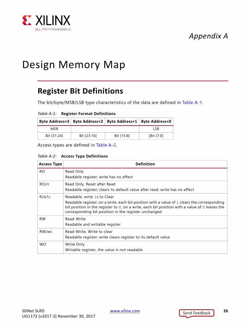
Register Bit DefinitionsThe bit/byte/MSB/LSB type characteristics of the data are defined in Table A-1.
Access types are defined in Table A-2.
Table A-1: Register Format DefinitionsByte Address+3 Byte Address+2 Byte Address+1 Byte Address+0
MSB LSBBit [31:24] Bit [23:16] Bit [15:8] [Bit [7:0]
Table A-2: Access Type DefinitionsAccess Type DefinitionRO Read Only
Readable register; write has no effectRO/rr Read Only, Reset after Read
Readable register; clears to default value after read; write has no effectR/w1c Readable, write 1s to Clear
Readable register; on a write, each bit position with a value of 1 clears the corresponding bit position in the register to 0; on a write, each bit position with a value of 0 leaves the corresponding bit position in the register unchanged
RW Read-WriteReadable and writable register
RW/wc Read-Write, Write to clearReadable register; write clears register to its default value
WO Write OnlyWritable register, the value is not readable
SDNet SLRD www.xilinx.com 26UG1172 (v2017.3) November 30, 2017
Send Feedback

Appendix A: Design Memory Map
Memory MapThe design register memory map is provided in Table A-3.
Register DescriptionCMAC Register MapAddress offsets, register descriptions, and reading mechanism are provided in the UltraScale Architecture Integrated Block for 100G Ethernet LogiCORE IP Product Guide (PG165) [Ref 2]. Some additional control and status registers, as well as DRP interface registers are required for the design phase, and are described in Table A-4.
Table A-3: Memory MapAddress Range Size (Bytes) Register Name/Brief Description
0x40000000 - 0x4000FFFF 64K CMAC0x40010000 - 0x4001FFFF 64K SDNet0x40020000 - 0x4002FFFF 64K Embedded TCAM0x40060000 - 0x40060FFF 4K Packet Player0x40200000 - 0x403FFFFF 2M Packet Capture0x80000000 - 0x80000FFF 4K Version Information0x80090000 - 0x80090FFF 4K Clock Monitor
Table A-4: CMAC Module RegistersRegister Address Name Type Initial
Value Bit(s) Range
Status Registers0xC000 tx_serdes_status RO 3:0 Tx_reset_done – If a bit is 1, the corresponding
SERDES tx_reset_done bit is asserted.0xC004 rx_serdes_status_0 RO 3:0 Rx_reset_done – If a bit is 1, the corresponding
SERDES rx_reset_done bit is asserted.0xC008 rx_serdes_status_1 RO 11:9 Rx_Buf_status for SERDES 3
8:6 Rx_Buf_status for SERDES 25:3 Rx_Buf_status for SERDES 12:0 Rx_Buf_status for SERDES 0
0xC00C debug_signals RO 20 CMAC Lbus Tx overflow24 CMAC Lbus Tx underflow
SDNet SLRD www.xilinx.com 27UG1172 (v2017.3) November 30, 2017
Send Feedback

Appendix A: Design Memory Map
CMAC GTY Registers0xD000 gty_tx_precursor RW 19:0 Each of the 4 GTYs has a 5-bit tx_precursor
input. GTY0 is bits 4:0, GTY1 bits 9:5, etc0xD004 gty_tx_postcursor RW 19:0 Each of the 4 GTYs has a 5-bit tx_postcursor
input. GTY0 is bits 4:0, GTY1 bits 9:5, etc0xD008 gty_tx_diffctrl RW 19:0 Each of the 4 GTYs has a 5-bit tx_diffctrl input.
GTY0 is bits 4:0, GTY1 bits 9:5, etc0xD00C gty_rx_lpmen RW 3:0 Rx LPM/DFE control for GTY. Each of the 4 GTYs
has a 1-bit rx_lpmen input. GTY0 is bit 0, GTY1 bit 1, etc.
0xD010 gty_loopback RW 11:0 GTY Loopback control. Each of the 4 GTYs has a 3-bit loopback control input. GTY0 is bits 2:0, GTY1 is bits 5:3, etc.• 000: Normal operation• 001: Near-end PCS loopback• 010: Near-end PMA loopback• 100: Far-end PMA loopback• 110: Far-end PCS loopback
CMAC/GTY DRP Registers0xE000 cmac_drp_addr_wdata WO 27 0: CMAC DRP write command
1: CMAC DRP read command25:16 CMAC DRP address to access15:0 Write data for CMAC DRP write port
0xE004 cmac_drp_read_data RO 15:0 Data read from CMAC DRP port0xE008 gty_drp_addr_wdata WO 29:28 GTY to Access (0 to 3)
27 0: GTY DRP write command1: GTY DRP read command
25:16 GTY DRP address to access15:0 Write data for GTY DRP write port
0xE00C gty_drp_read_data RO 15:0 Data read from GTY DRP port0xE010 cmn_drp_addr_wdata WO 27 0: Common DRP write command
1: Common DRP read command25:16 Common DRP address to access15:0 Write data for Common DRP write port
0xE014 cmn_drp_read_data RO 15:0 Data read from Common DRP port
Table A-4: CMAC Module Registers (Cont’d)Register Address Name Type Initial
Value Bit(s) Range
SDNet SLRD www.xilinx.com 28UG1172 (v2017.3) November 30, 2017
Send Feedback

Appendix A: Design Memory Map
Embedded TCAM Register MapThe Embedded TCAM register map is provided in Table A-5.
Miscellaneous Registers0xF000 lbus_conv_s2n_flags RO 4 EOP Address FIFO Full on seg to non-seg LBUS
converter3 RAM 3 collision on seg to non-seg LBUS
converter2 RAM 2 collision on seg to non-seg LBUS
converter1 RAM 1 collision on seg to non-seg LBUS
converter0 RAM 0 collision on seg to non-seg LBUS
converter0xF004 lbus_conv_n2s_flags RO 1 EOP Address FIFO Full on non-seg to seg LBUS
converter0 Data FIFO Full on non-seg to seg LBUS
converter
Table A-4: CMAC Module Registers (Cont’d)Register Address Name Type Initial
Value Bit(s) Range
Table A-5: Embedded TCAM Register MapRegister Address Name Type Initial
Value Bit(s) Range
Control Registers0x0000 device_id RO 31:0 Unique device ID0x0040 update_request RW 29:28 Command request:
• 00: Read the contents of the TCAM's Valid, Key, Mask and Value registers at the address specified in bits 15:0
• 01: Write the contents of the Valid, Key, Mask and Value registers to the TCAM at the address specified in bits 15:0
• 10: Initialize the TCAM15:0 Address of read/write operation
0x0044 update_response RO 0 Asserted when TCAM detects a write to the update_request register
0x004C valid RW 0 Indicates TCAM entry is Valid0x0050-0x0074
data RW 0 Data registers containing Key of max-width 320-bits
SDNet SLRD www.xilinx.com 29UG1172 (v2017.3) November 30, 2017
Send Feedback

Appendix A: Design Memory Map
Packet Player Register MapThe Packet Player register map is provided in Table A-6.
0x0080-0x00A4
mask RW 0 Data registers containing Mask of max-width 320-bits
0x00E0-0x00FC
value RW 0 Data registers containing Value of max-width 256-bits
Table A-5: Embedded TCAM Register Map (Cont’d)Register Address Name Type Initial
Value Bit(s) Range
Table A-6: Packet Player Register MapRegister Address Name Type Initial
Value Bit(s) Range
Control Registers0x0000 packet_player_ctrl RW 1 0: Packet player sends all packets in memory
once1: Packet player continuously cycles through stored packets
0 Enable packet player when is set to 10x0004 packet_player_write WO 28 Write data in packet_player_data to shadow
BRAM when set to 124 Toggle pointer to packet/shadow memory
23:20 Header data19:0 Shadow memory address to which
packet_player_data is written0x0008 packet_player_data WO 31:0 Packet data to be written into BRAM
Status Registers0x000C packet_player_status RO 1 Active memory pointer – shows which half of the
packet player's memory is used as packet memory.
0 Set to 1 when the packet player has finished sending packets. This bit is automatically cleared when read.
0x0010 packet_player_cnt RO 31:0 A count of the number of packets transmitted by the packet player. This counter automatically rolls over. This counter is automatically cleared on the packet player enable’s rising edge.
0x0100 enable_sdnet_bypass RW 0 0: Data from packet player/CMAC is routed into SDNet1: Data from packet player/CMAC is routed directly to packet capture/CMAC
SDNet SLRD www.xilinx.com 30UG1172 (v2017.3) November 30, 2017
Send Feedback

Appendix A: Design Memory Map
Packet Capture Register MapThe Packet Capture register map is provided in Table A-7.
Table A-7: Packet Capture Register MapRegister Address Name Type Initial
Value Bit(s) Range
Data0x00000- 0x1FFFDF
packet_capture_data RO 31:0 This data needs to be read and stored in an ASCII file for packet capture data analysis.
Control Registers0x1FFFE0 packet_capture_ctrl RW 2:1 00: CMAC controls the RDY signal
01: Packet capture is the only data sink; it sets RDY 50% of the time in pseudo random mode10: illegal11: Packet capture is the only data sink; it sets RDY 100% of the time
0 Enable packet capture when set to 1.Status Registers
0x1FFFE8 packet_capture_status RO 5 Set to 1 when another packet arrives when the packet capture buffer is already full. This bit is automatically cleared when the packet capture is disabled.
4 Set to 1 when there was insufficient space to store the final packet. This bit is automatically cleared when the packet capture is disabled.
1 Set to 1 when there is no activity on the packet capture module's LBUS interface for MemorySize x 8/ BUSWidth clock cycles. This bit is automatically cleared when the packet capture is disabled.
0 Set to 1 when the packet capture buffer is full. This bit is automatically cleared when the packet capture is disabled.
0x1FFFF0 packet_capture_cnt RO 31:0 Count of the number of complete packets stored in the packet capture buffer. This counter gets the correct count value when the packet capture is disabled, and it maintains that value until enabled and disabled again.
SDNet SLRD www.xilinx.com 31UG1172 (v2017.3) November 30, 2017
Send Feedback

Appendix A: Design Memory Map
Version InformationThe Version Information register map is provided in Table A-8.
Table A-8: Version Information Register MapRegister Address Name Type Initial
Value Bit(s) Range
0x0000 version_id RO 31 0: Design does not contain full licensed IP1: Design contains full licensed IP
23:16 Major version number15:0 Minor version number
0x0004 board_id RO 0x0 31:30 Stepping level:00: Stepping level 001: Stepping level 110: Stepping level 211: Stepping level 3
0x0 29:28 Silicon revision:00: ES101: ES210: Production
0x0 27:24 Board revision:0000: Rev A0001: Rev B0010: Rev C0011: Rev 1.00100: Rev 1.1
0x00 23:16 Board Type in hex:0x00: VCU0x01: KCU0x02: ZCU0x10: VC0x11: KC0x12: ZC
0x110 15:0 Board Number in hex0x0008 vivado_id RO 0x0 31:16 Date of Vivado internal build, if used: Set to
0x0000 if the official Vivado build is used. Otherwise 23:16 represents day of internal build, 31:24 represents month of internal build.For example: 0x0610 indicates that the Vivado internal build from the 10th of June was used.
0x14 11:4 Vivado major version number in hex0x4 3:0 Vivado minor version number in hex
0x000C scratch pad RW 31:0 Read data is inverse of last value written
SDNet SLRD www.xilinx.com 32UG1172 (v2017.3) November 30, 2017
Send Feedback

Appendix A: Design Memory Map
Clock MonitorThe Clock Monitor register map is provided in Table A-9.
0x0010 design_id RO 0x1 31:16 IPDS Category:0x2000: Development
0x1 15:0 IPDS Project Number:0x3104: SDNet SLRD
Table A-8: Version Information Register Map (Cont’d)Register Address Name Type Initial
Value Bit(s) Range
Table A-9: Clock Monitor Register MapRegister Address Name Type Initial
Value Bit(s) Range
0x0000 clk1_frequency RO 31:0 SI570 frequency0x0004 clk2_frequency RO 31:0 Reserved0x0008 clk3_frequency RO 31:0 CMAC0 txusrclk20x000C clk4_frequency RO 31:0 Reserved0x0010 clk5_frequency RO 31:0 pcie_axi_clk0x0014 clk6_frequency RO 31:0 Clock 170 MHz
SDNet SLRD www.xilinx.com 33UG1172 (v2017.3) November 30, 2017
Send Feedback

Appendix B
Design Blocks Detailed Description
CAUI-4 CMACThe CMAC wrapper consists of the CMAC LogiCore IP, the CMAC statistics gathering unit and an AXI register interface for controlling and monitoring the CMAC LogiCore IP (see Figure B-1). The LogiCore contains the four GTY transceivers running at 25.78125 Gb/s which interface to a CFP4 LR4 optical module on the board.
LBUS Converter (S2N and N2S Converter)This block converts LBUS signals between four 128-bit segments of the LBUS on CMAC side and one 512-bit segment LBUS required for SDNet operation. There are no AXI control or status registers in this block. The CMAC side of the block uses the 322 MHz clock (or optional 300 MHz clock for the internal testing mode), and the SDNet side of the converter uses the 300 MHz clock. Synchronization between clock domains is performed in asynchronous FIFO blocks. Separate resets are provided for each of these clock domains.
X-Ref Target - Figure B-1
Figure B-1: CMAC Wrapper
CMAC LogiCore
Statistics Gathering
Register Interface
SDNet SLRD www.xilinx.com 34UG1172 (v2017.3) November 30, 2017
Send Feedback

Appendix B: Design Blocks Detailed Description
Packet PlayerThe packet player is a test block used for internal testing mode when no external test equipment is available or required. These are the main packet player features:
• By default, packets are stored in 128 KB internal RAM (excluding header). The MemorySize parameter can be set to change the packet player's memory size to 32 KB, 64 KB, 256 KB, 512 KB, or 1 MB.
• LBUS width is set to 512 bits by default. The LBUSWidth parameter can be set to change the packet player's LBUS width to 64, 128, 256, 1024, 2048, or 4096 bits.
• One half of the RAM is used for transmitting packets, while the other is shadow memory to which new packet data can be written via the AXI interface.
• The packet/shadow memory pointer can be toggled via the AXI interface.• Packets in RAM can have any size that does not exceed RAM capacity.• RAM memory can only contain full packets and not fractions of packets.• Both packet and shadow memory are pre-loaded with a RAM initialization file.• Packet and shadow memory are not readable via AXI.• Packet player can be enabled and disabled via the AXI register interface.• Status (INACTIVE, IN PROGRESS, DONE) is readable via the AXI register interface.• SDNet bypass mode is controlled from packet player.• The number of packets transmitted is available.
Packet Player Control and StatusPacket player activity is controlled by writing to packet_player_ctr, as defined in Packet Player Register Map, page 30. Writing to bit 1 determines whether packets stored in memory are sent only once or continuously, by cycling through packet memory. Writing 1 to bit 0 enables transmission of packets from the packet player. After packet player finishes its transmission, which can be checked by reading the packet_player_status register, it is necessary to reset bit 0 before enabling packet player again.
Packet player can be enabled in either single or continuous mode, but when disabling it, it is important to set it to single mode prior to disabling it completely, to transmit all of the packets from memory. Upon completion, packet player indicates its status in the packet_player_status register and can be disabled.
Packet player also gives the option to bypass SDNet for data path by writing a 1 to the enable_sdnet_bypass register. This is used for test purposes only.
SDNet SLRD www.xilinx.com 35UG1172 (v2017.3) November 30, 2017
Send Feedback

Appendix B: Design Blocks Detailed Description
The number of packets transmitted by packet player can be read from the packet_player_cnt register.
Packet/shadow RAM InterfaceBRAM is used to store packet data that is sent to SDNet via the LBUSWidth bits-wide LBUS interface. This RAM is organized as a 36 bits-wide write interface with a depth of MemorySize/4 words and a 9/8 x LBUSWidth bits-wide read interface with depth of MemorySize x 8/ BUSWidth words. For descriptive purposes, the write side word is called AXI word and the read side is called LBUS word in the following text.
Memory is broken into two halves – Packet Memory is used to generate packets for the LBUS interface (read only), and Shadow Memory is used to write new packet data (write only). Software can swap the two memory halves, thus providing LBUS with new packet data that software has previously written into memory through the AXI interface.
Each LBUS word and control consists of LBUSWidth/32 36-bit words such that bits 31:0 of the word contains packet data, while bits 35:32 of the ord contains header info. Header info can be SOP, EOP, ERR, or MTY[11:0], or unused bits, depending on the memory location of the AXI word. An example of the header field layout over a single 512-bit LBUS cycle (16-36-bit words) is shown in Table B-1.
Packet data must be generated in K12 format. Perl scripts are provided to translate packet data into .mif files for memory initialization, or software-writable format to overwrite the shadow memory.
The sequence for writing data to shadow memory is:
• 32 bit data word is written to packet_player_data register, see Packet Player Register Map, page 30.
• Control word is written to packet_player_write register, see Packet Player Register Map, page 30. This word contains commands for shadow memory write, swapping shadow
Table B-1: Packet Player RAM SectionAddress mod 16
Header (35:32) Header Comment
0x0 EES Bit 3: 0Bit 2: ERRBit 1: EOPBit 0: SOP
0x1 MTY[3:0] Number of empty packets, bits 0 to 30x2 MTY[7:4] Number of empty packets, bits 4 to 70x3 MTY[11:8] Number of empty packets, bits 8 to 110x4-0xE N/A Unused0xF PE Packets End – set to 1 only for the last packet in memory
SDNet SLRD www.xilinx.com 36UG1172 (v2017.3) November 30, 2017
Send Feedback

Appendix B: Design Blocks Detailed Description
and packet data memory, header information, and data write address. If a shadow memory write command was issued to this register, header info and the data word is written to the address specified in the packet_player_write register.
SDNet-generated Packet Processor SmartCOREThe SmartCORE packet processor is a test core. Refer to SDNet-generated SmartCORE, page 10 and Packet Player, page 35 for further descriptions of the SmartCORE examples provided by this SLRD.
Packet CapturePacket capture is a test block used for internal testing mode when no external test equipment is available or required. These are the main features of the block:
• Stores processed packets into internal RAM. Default RAM size (excluding header) is 128 KB, but it can be set to 32 KB, 64 B, 256 KB, 512 KB, or 1 MB using packet capture's MemorySize parameter
• Stores up to MemorySize x 8/LBUSWidth LBUS cycles of data (with a 512 bit wide LBUS, 128 KB memory size, and 64 B packets, this is equal to 2,048 packets, for 65B–128B packets, that is 1,024 packets, etc.)
• Packet memory can be read via the AXI bus• Status and number of packets received can be read via the AXI bus• Capturing data can be enabled/disabled via the AXI register interface• Has the option of setting the RDY signal at a 50% duty cycle in pseudo-random pattern
to mimic back pressure from the CMAC TX (150M packets per second)
Packet Capture Control and StatusOnce enabled, the packet_capture_status register can be read (see Packet Capture Register Map, page 31). Register packet_capture_cnt contains the number of packets packet capture received during the last enabled period.
Bits 2 and 1 of the Packet Capture Control register allow packet capture to be used as the only data sink and to control the frequency of the RDY signal (back pressure).
Test flags from LBUS converter are also available for reading from the packet capture block via the AXI interface.
SDNet SLRD www.xilinx.com 37UG1172 (v2017.3) November 30, 2017
Send Feedback

Appendix B: Design Blocks Detailed Description
Packet RAM InterfaceThe LBUS (write) side of the RAM interface uses a 9/8 x LBUSWidth bits-wide bus, LBUSWidth bits being data and the remainder being header and unused bits. The AXI (read) side of the RAM interface uses 32-bit words. LBUSWidth x 2/32 AXI register locations represent one LBUS data cycle. The following is an example for a 512 bit-wide LBUS:
• All even locations represent data, starting from the most significant bit (MSB) (location 0 contains data bits 511:480, etc.)
• All odd locations represent headers starting from the least significant bit (LSB). See Table B-1.
Once data is read from memory, the Perl script can be used to translate it to K12 format.
Table B-1.
Table B-2: Packet Capturer RAM SectionAddress mod 16
Header (35:32) Header Comment
0x1 EES Bit 3: 0Bit 2: ERRBit 1: EOPBit 0: SOP
0x3 MTY[3:0] End Of packet0x5 MTY[7:4] Packet error0x7 MTY[11:8] Number of empty packets, bits 8 to 110x9-0x1F N/A Unused
SDNet SLRD www.xilinx.com 38UG1172 (v2017.3) November 30, 2017
Send Feedback

Appendix C
Additional Resources and Legal Notices
Xilinx ResourcesFor support resources such as Answers, Documentation, Downloads, and Forums, see Xilinx Support.
Solution CentersSee the Xilinx Solution Centers for support on devices, software tools, and intellectual property at all stages of the design cycle. Topics include design assistance, advisories, and troubleshooting tips.
References1. SDNet Packet Processor User Guide (UG1012)2. UltraScale Architecture Integrated Block for 100 G Ethernet LogiCORE IP Product Guide
(PG165)3. VCU110 Evaluation Board User Guide (UG1073)
Please Read: Important Legal NoticesThe information disclosed to you hereunder (the “Materials”) is provided solely for the selection and use of Xilinx products. To the maximum extent permitted by applicable law: (1) Materials are made available "AS IS" and with all faults, Xilinx hereby DISCLAIMS ALL WARRANTIES AND CONDITIONS, EXPRESS, IMPLIED, OR STATUTORY, INCLUDING BUT NOT LIMITED TO WARRANTIES OF MERCHANTABILITY, NON-INFRINGEMENT, OR FITNESS FOR ANY PARTICULAR PURPOSE; and (2) Xilinx shall not be liable (whether in contract or tort, including negligence, or under any other theory of liability) for any loss or damage of any kind or nature related to, arising under, or in connection with, the Materials (including your use of the Materials), including for any direct, indirect, special, incidental, or consequential loss or damage (including loss of data, profits, goodwill, or any type of loss or damage suffered as a result of any action brought by a third party) even if such damage or loss was reasonably foreseeable or Xilinx had been advised of the possibility of the same. Xilinx assumes no obligation to correct any errors contained in the Materials or to notify you of updates to the Materials or to product specifications. You may not reproduce, modify, distribute, or publicly display the Materials without prior written consent. Certain products are subject to the terms and conditions of Xilinx’s limited warranty, please refer to Xilinx’s Terms of Sale which can be viewed at http://www.xilinx.com/legal.htm#tos; IP cores may be subject to warranty and support terms contained in a license issued to you by Xilinx. Xilinx products are not designed or intended to be
SDNet SLRD www.xilinx.com 39UG1172 (v2017.3) November 30, 2017
Send Feedback
Appendix C: Additional Resources and Legal Notices
fail-safe or for use in any application requiring fail-safe performance; you assume sole risk and liability for use of Xilinx products in such critical applications, please refer to Xilinx’s Terms of Sale which can be viewed at http://www.xilinx.com/legal.htm#tos.NOTICE: This pre-release document contains confidential and proprietary information of Xilinx, Inc. and is being disclosed to you as a participant in an early access program, under obligation of confidentiality. You may print one (1) copy of this document for evaluation purposes. You may not modify, distribute, or disclose this material to anyone, including your employees, coworkers, or contractors (these individuals must apply for separate access to the program). This document contains preliminary information and is subject to change without notice. Information provided herein relates to products and/or services not yet available for sale, and provided solely for information purposes and are not intended, or to be construed, as an offer for sale or an attempted commercialization of the products and/or services referred to herein.© Copyright 2016-2017 Xilinx, Inc. Xilinx, the Xilinx logo, Artix, ISE, Kintex, Spartan, Virtex, Vivado, Zynq, and other designated brands included herein are trademarks of Xilinx in the United States and other countries. All other trademarks are the property of their respective owners.
SDNet SLRD www.xilinx.com 40UG1172 (v2017.3) November 30, 2017
Send Feedback