secondary electron emission yields*
TRANSCRIPT

SECONDARY ELECTRON EMISSION YIELDS*
I. Krainsky, W. Lundin, W. L. Gordon, and R. W. Hoffman Case Western Reserve University
SUMMARY
The secondary electron emission characteristics for a variety of space- craft materials have been determined under UHV conditions using a commercial double pass CMA which permits sequential Auger electron spectroscopic analysis of the surface. We have examined the transparent conductive coating indium tin oxide (ITO) on Kapton and borosilicate glass and indium oxide (10) on FEP Teflon. Total yields vary slightly with samples and with substrates. The total SEE coefficient, Omax, Zanges from 2.5 to 2.6 on as-received surfaces and from 1.5 to 1.6 on Ar sputtered surfaces with < 5 nm removed.
For these measurements a cylindrical sample carousel provides normal inci- dence of the primary beam as well as a multiple Faraday cup measurement of the Q nA beam currents. Total and true secondary yields are obtained from target current measurements with biasing of the carousel. A primary beam pulsed mode to reduce electron beam dosage and minimize charging of insulating coatings has been applied to MgF coated solar cell covers.
2
Electron beam effects on IT0 were found quite important at the urrent densities necessary to do Auger studies (0.6 PA minimum or 2. 1 x lo-' ~/cm') but relatively unimportant at the 10 nA levels used in short exposure methods or pulsed methods (150 nA peak, 2 us) for obtaining SEE coefficients. Angle of incidence dependence for I0 on FEP Teflon has been obtained for 0.5 < EP < 5.0 keV.
INTRODUCTION
One result of the current interest in spacecraft charging pehnomena has been the development in 1978 by NASA of a computer code - NASCAP - capable of providing a detailed picture of the charging process for realistic three-di- mensional models of spacecraft (ref. 1). Amajor impediment to the use of NAS- CAP is the paucity of data for the secondary electron emission characteristics of actual spacecraft materials. Methods for obtaining these data from well- characterized surfaces using a commercial cylindrical mirror analyzer (CMA) were developed, tested on clean Ag and Cu surfaces, and applied to aluminum alloys with varying surface treatments typical of those used on spacecraft (ref. 2). Target current measurements gave electron yield data as a function of primary energy, EP. The CMA provided both the surface composition and the secondary electron energy distributions, N(E), for a given EP from integration of the CMA output, operating in the standard derivative mode.
To overcome severe charging effects experienced with a thick insulating coating such as anodized samples we have developed a pulsed beam technique using sufficiently low dosage to permit measurements on thin insulating layers.
"work performed under NASA Grant No. NSG-3197 179

This method, together with that of short DC exposures to the primary beam, has been used to obtain secondary yields from thin (Q 20 nm) transparent conducting coatings, indium-tin oxide (ITO), on three insulating substrates: borosilicate glass, Kapton, FEP Teflon, and MgF2 on quartz. The influence of electron beam dosage effects has been explored in order to extrapolate the results back to typical current densities at the spacecraft surfaces. The effect of mild Ar ion sputtering of as-received surfaces has also been observed as a guide to changes in yield which may occur under prolonged plasma exposure in space. Secondary electron yields for 0.5 keV < EP < 5 keV have been measured at vary- ing angles of incidence.
EXPERIMENTAL TECHNIQUES AND MODIFICATIONS
The electrons below 50 eV are usually termed "true secondaries" and the electrons above 50 eV termed "backscattered" (ref. 3). Thus, the true SEE co- efficient d is just the number of true secondaries emitted per primary electron. Typically, measurements of conducting surfaces involve determination of the target current under two conditions: I+, where backscattered electrons are re- jected (biasing the target at + 50 V relative to the grounded surroundings) and I , where all outgoing electrons are rejected (biasing the target at - 50 V). ~ 6 e primary current, Ip, is found by displacing the carousel so that the beam enters the Faraday cup. As noted in reference2, d = (I+ - I-)/I to a good approximation while the total SEE coefficient 0 = 1 - 1-11 and kcludes elas- tically and inelastically backscattered electrons in addityon to the true secondaries.
With thick insulating layers on the target surface, charging will take place, where the sign of the charge depends on whether a is 3 1. For our geo- metry, the CMA entrance grid subtends an angle of 1.5 IT steradians and is always grounded. Thus electric fields are developed as the target surface be- comes charged.
Pulsed Beam Techniques
To minimize charging effects on insulating layers as described above, we have introduced a pulsed beam technique together with a low energy electron flood gun to restore the surface to an uncharged state. If a single square current pulse of length T is incident on the insulator layer mounted on the target and the target is biased negatively to repel all secondaries then, re- ferring to the equivalent circuit(figure l(a)), the charge accumulated on the target is 'I
q = I- dt = TI - and the potential drop across the input capacitor 0
Ci is V- = q/Ci= TI - /Ci Hence, as defined earlier, the total SEE coefficient - 1-V-/vp. By observing V- for a series of pulses at fixed EP, the
ir~s:&'k charging effects can be observed as a monotonic change in its value. Exposure of 'the surface of the insulating layer to low energy electrons from a flood gun will then restore the surface to a nearly uncharged state. Pulse measurements with +50 V applied to the target provide I+ so that n might be determined as well.

Beam pulses were produced through puls ing a beam blanking c i r c u i t . The process i s i l l u s t r a t e d schematical ly in f i g u r e l ( b ) . S ingle pulses from t h e pulse generator d r i v e the blanking c i r c u i t which i n t u r n con t ro l s t h e elec- t r o n gun e x t r a c t o r p o t e n t i a l . Target current pulses a r e t y p i c a l l y 2 ys dura- t i o n with a 0.2 ps rise t i m e . They are r e g i s t e r e d by a sample-and-hold c i r - c u i t f o r measurements by a DVM. The o r ig ina l pu l ses a r e s t r e t ched i n time by a high input impedance fol lower, amplified by a f a c t o r of 100, and then e n t e r t h e sample-and-hold c i r c u i t .
Methods used f o r Secondary Yield Measurements
A - Short exposure t o t h e primary beam
In measurements of secondary y ie ld from conducting surfaces , DC exposure t o t h e primary beam i s a s tandard prac t ice . To avoid over-exposure t o t h e beam, p a r t i c u l a r l y i n t h e case of t ransparent conducting coat ings , we have been care- f u l t o l i m i t exposure time t o a minimum, cons i s t en t with t h e observation of adequate s igna l s . Thus we have used the beam b l a n k i n g . c i r c u i t i n a manual opera t ion mode t o l i m i t t he t i m e on the sample t o 1 t o 2 seconds. Af ter com-
p l e t i n g beam alignment and focus of the primary beam, I is measured using P
t h e Faraday cup. The beam i s then c u t o f f and t h e carousel t r a n s l a t e d so t h a t t h e beam w i l l s t r i k e t h e sample a t t h e new des i red locat ion . With t h e t a r g e t biased a t +50 V, I+ is found by disengaging t h e beam blanking c i r c u i t f o r Q 2 sec. The ammeter response time is 'L 1 sec. The t a r g e t is then biased t o -50 V and I- i s found in another 2 t o 3 sec. in t e rva l . F ina l ly , t h e carousel i s t r ans la ted t o bring t h e beam i n t o t h e Faraday cup and aga in disengaging t h e blanking c i r c u i t t o permit a second measurement of Ip. This procedure is repeated f o r each requi red v a l u e of EP.
From t h i s series of measurements we o b t a i n both a and 6 a s defined ear- l i e r . Also, by scanning across the Faraday cup w e determine t h a t the beam diameter is % 2 mm. Typical primary currents ranged from 1 t o 10 nA.
B - Pulsed beam measurements
A manually pulsed beam is employed, as described earlier, f o r t h e study of i n s u l a t i n g surfaces and t o avoid beam damage with conducting surfaces. The value of Ip i s determined wi th t h e Faraday cup i n place. During t h i s t i m e t h e beam is operated i n a chopped mode t o allow center ing on t h e cup. A t y p i c a l maximum value of the cu r ren t pulses i s % 50 nA. After blanking, the carousel is s h i f t e d s o t h a t beam w i l l s t r i k e the des i red loca t ion on the sample. Then, with the t a r g e t biased a t -50 V r e l a t i v e t o ground a 2 psec pulse is del ivered and t h e value of I- on t h e sample-and-hold c i r c u i t read from the DVM. Repeti- t i o n of a s i n g l e pulse i n t h e region where U > 1 provides a quick t e s t f o r charging, s i n c e Qobs will drop monotonically i f charging is present . I n t h e presence of charging, use of the low energy f lood gun between pulses a s su res t h a t the sample su r face is res tored t o its uncharged s t a t e , but does not guar- an tee the absence of charging during an ind iv idua l pulse nor avoid f i e l d g rad ien t s i n the sample near-surface region. Tes t ing f o r charging i n t h i s l a t t e r case can be done by reducing pulse he ight and width and comparing the 0

values obtained. At present, noise in the sample-and-hold circuit limits us to a pulse height of 12 nA in I .
P
Generally, only I- was measured in this mode so the backscatter coeffici- ent, n, was not obtained. Since n is not a large fraction of a for insulators of low atomic number and is relatively constant in energy above a few hundred volts, an estimated value can be assigned without introducing serious. Z-depen- dent uncertainties.
MATERIALS EXAMINED
Samples of three insulating materials, Kapton, FEP Teflon, and borosili- cate glass coated with indium tin oxide (ITO) by the General Electric Company were provided to W. L. Lehn of the Air Force Materials Lab, Wright Patterson Air Force Base. Reactive sputtering techniques (ref. 4) were employed using a magnetron sputter gun, In/Sn targets and an oxygen + argon atmosphere. The compositions are nominally 90% In203 and 10% Sn02 but the stoichiometries are uncertain. IT0 film conductivity generally increases with the density of oxy- gen defects (ref. 5).
Table I gives a summary of the types of samples studied with nominal IT0 thickness and back surface coating listed. We found that the IT0 coating on the FEP sample had a very high-to-infinite resistance and showed sufficient charging that we could not make an Auger determination of In, Sn, or 0 present on the surface. An indium oxide (10) coating, found by GE to be more com- patible with FEP Teflon (ref. 6) was obtained. It had been prepared in essen- tially the same manner as the IT0 coating. Samples are % 1 cm x 1 cm, cut from 10 cm x 10 cm sheets of IT0 on Kapton of I0 on FEP Teflon and from 2.5 cm x 2.5 cm tiles of IT0 on borosilicate glass with individual samples identified. All samples were inserted into the UHV system without prior sur- face cleaning except for blow-dusting with Freon gas.
The relative amount of In, Sn, and 0 in ITO, as well as other contaminants were obtained by AES methods. A surface contamination layer was present which increased the secondary yield compared to samples from which the contamination layer had been removed by Ar ion sputtering.
As a comparison with commercially available transparent conducting coat- ings (TCC) films, samples were obtained from Sheldahl. No nominal composition was supplied but our Auger analysis indicated the major components of TCC on Kapton were In, Sn, and 0 plus contamination.
MgF2 coatings on quartz substrates were obtained from OCLI, and data ob- tained from both the coated and uncoated surfaces of the solar cell super- strates.
RESULTS AND DISCUSSION
The results will focus on yield data and include figures of o(E) and/or 6(E) for various coatings. Results of a study of the influence of the electron beam and sputtering of samples are included.

Indium Tin Oxide Coatings
These data, in contrast with later pulsed results, have the advantage of containing both the total SEE coefficient, a and true SEE coefficient 6 so are presented first, although they do represent a greater net exposure to the elec- tron beam than do our pulse measurements. Furthermore, we note that earlier data obtained in this system for the SEE backscatter coefficient, q, of Ag ran (ref. 2) about 35% below the accepted value. The reason for this discrepancy has not been determined but may be related to field distortions between the carousel and its surroundings during L+ measurements. Thus, we place greater emphasis on the a values obtained here.
Typical results for as-received surfaces of IT0 on Kapton and borosilicate glass and I0 on FEP Teflon are presented in figures 2, 3, and 4. Primary beam currents and current densities are provided with each figure and SEE para- meters tabulated. Particular samples cut from the sheet initially provided to us are identified for future reference. The current density values are only approximate since the beam profile is not rectangular. The data are remark- ably similar considering the range of samples. Figure 5 presents the normal- ized 6 curves.
Differencesbetween measurernentsonnominally similar specimens introduce the general question of reproducibility. Surface contaminants are the most important factor but surface roughness, general composition (particularly the variation in conductivity associated with varying 0 concentration), and elec- tron beam effects cannot be neglected. 6 values obtained from three different locations on a single sample of I0 on FEP and the variation for two different samples of IT0 on borosilicate glass are small. We conclude that the uncer- tainties in a given measurement of 6 (and a) are approximately + 0.1 with - variations among samples occasionally outside this range.
The total SEE coefficient for the as-received surface of typical samples of Sheldahl TCC on Kapton and Teflon is not significantly different from the SEE coefficients from the GE as-received surfaces.
A comparison between pulsed beam and short exposure results for the GE samples was made using normalized curves to minimize the effect of variations among different samples of the same material and of possible effects of elec- tron beam dosage as considered later. With the possible exception of I0 on FEP Teflon no differences were encountered.
Magnesium Fluoride Coated Solar Cell Covers
MgF2 on fused silica required the pulsed beam technique because of the high (essentially infinite) sample resistance. In spite of the charging ob- served during SEE measurements, AES spectra were obtained without shifts of
'~ronshtein (ref. 7) using a 4r collector geometry, quotes values of 0.38 at 1 kV and 0.41 at 4 kV while our values were 0.25 and 0.27 at these primary ener- gies, with the 1.5 IT solid angle geometry of our apparatus.

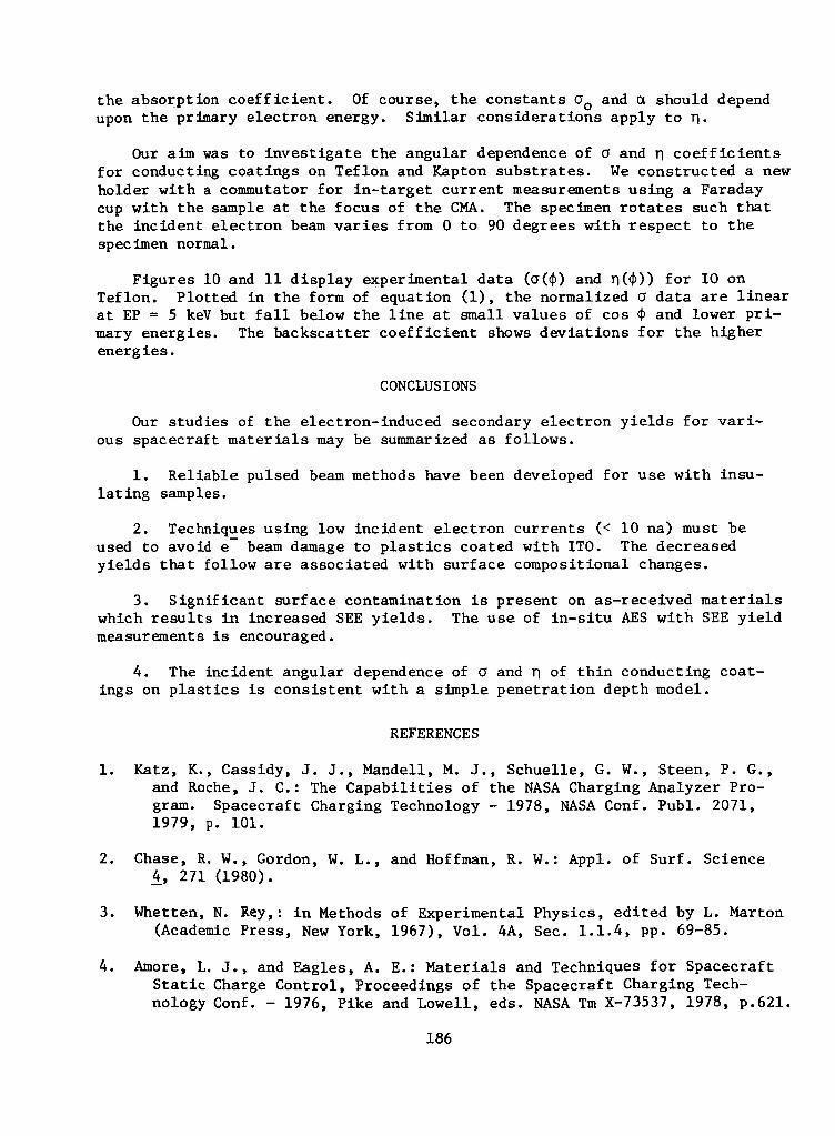
the Mg and F peaks, but AES spectra were not obtainable from the other side due to charging. Because of possible identification difficulties in coding of the coated side, both the MgF2 and quartz surfaces of the OCLI standard solar cell covers were examined. Figures 6 and 7 present the 6 and cr data obtained for the MgF2 and fused silica surfaces, respectively. All datawereobtained by the pulsed beam method in which I+ and I- were directly measured with + 50 V potentials on the target. The data for the fused silica side are quite stable when compared to earlier samples, but the MgF2 surface appears erratic. These data must be regarded as preliminary as we are not certain of the origin of the variations. As a result we have not listed the yield parameters.
Surface Contamination of IT0 Coatings
The influence of surface contamination is best illustrated by comparison of SEE coefficients before and after argon ion sputtering. We examine these after presenting the AES evidence for a change in surface composition with sputtering. Auger spectra taken before sputtering of IT0 on Kapton and I0 on FEP Teflon show the presence of similar contaminants - C, S, C1 - on each of the as-received surfaces. After ~ r + sputtering of Q, 1 nm of the nominal 20 nm of IT0 on Kapton film, there is little change in concentration except for the expected appearance of Ar and an increase in S. This particular increase cor- related with results to be discussed later under electron beam damage. After Q, 4 nm has been sputtered away (on a different sample) IT0 on Kapton exhibits a significant clean-up of the surface contaminants. The In/Sn concentration increased but may be an artifact or a depth effect or be sample-dependent. This requires further study, as does our assumption that the 4 nm sputtering produces a "clean" IT0 surface. It is, however, consistent with the results of electron beam damage studies discussed later.
Figure 8 shows the large changes in 6 values as a result of sputtering. The enhancement of the SEE coefficients due to contamination which exists prior to sputtering is evident and merits further study. Normalization of the 6 curves emphasizes a relative decrease in the high EP values for 6 with in- creased sputtering. This difference is unexpected, in the sense that the true SEE coefficients for most materials fit a commonnormalizedyield curve.
Electron Beam Effects
Electron beam effects on surface composition have been well documented in the past, particularly in the case of Auger analysis where the measurement pro- cess can perturb the results. Such effects have a two-fold relevance to the present study. First, a knowledge of surface composition is essential to the general characterization of the surface for correlation with secondary emission yield. Second, the SEE coefficients (which are measured at a much lower cur- rent density than that used for Auger data) depend on electron beam effects. This, in turn, requires a detailed evaluation to predict their applicability to spacecraft charging.
In our preliminary studies of the SEE coefficients of ITO, we discovered that the values were dependent on whether the area under investigation had been previously exposed, as for example, in focussing the primary beam or in

previous Auger studies. After becoming aware of this problem we took data in the short exposure mode as outlined earlier and, when the pulsed beam circuit was available, we used this technique in the majority of cases to minimize dosages. This approach still does not provide a satisfactory answer to the question of the applicability of our results to spacecraft, in view of the extremely low current density in the plasma environment of the craft. To this end, we carried out an investigation of the electron beam dosage dependence of a and of the Auger measurements of surface composition. This was accomplished by observing the time dependence of the parameter in question at a series of different primary current values, operating in the DC mode.
Measurements of ~ ( t ) at a given current were done at an EP of 3 keV so that they are beyond EPmX. The primary electron gun was well stabilized be- fore data were taken with the target biased at -50 V relative to ground. The beam size was determined in a position scan across the Faraday cup and typi- cally had a diameter of 'L 0.8 mm. A series of a(t) values were obtained at each of 6 different values of Ip ranging from 10 nA to 36 @. Ip was checked before and after a given series of ~ ( t ) measurements at that current to cor- rect for a slight monotonic drift (Q 2%) which continued to occur. Results are displayed in figure 9 with data points from 0.1 min to % 120 min at each current. The earliest points are not indicated because of the difficulty of displaying the time scale appropriately but all values began at or near a 0 of 1.25 to 1.3. Thus, while not shown, rapid drops in a occurred, particularly at the higher currents. The 55 nA current curve started from a value close to that of the others but dropped abruptly to the "plateau" shown in figure 9. This effect has not been observed at other locations on the sample with other current levels nor has the reproducibility of the 55 nA result been checked. Wherever tested, we note that the effects illustrated here are not reversible with time.
For all Ip > 0.6 @ an obvious discoloration developed with a diameter about equal to the e' beam spot area of 5 x cm2. At the higher currents (36 @) perforation of the Teflon substrate resulted from the thermal damage. We speculate that contaminants, especially S, are brought to the surface and lead to a decreased secondary yield.
Angular Dependence of SEE Yield
It is well known that for metals as well as for semiconductors SEE co- efficient a increases with increasing incident angle $I of the primary beam (ref. 7). In accordance with Bruining (ref. 8), primary electrons moving in straight paths penetrate to a smaller depth normal to the surface when the angle is slanting. Thus, secondary electrons are generated on the average at smaller depth and have an increased probability of escape. As a re- sult a is larger. Simple calculations based on this consideration give,the following dependence of a coefficient on the incident angle, $I, relative to the specimen normal.
where x is the penetration length measured along the incident path, and a is
t h e absorp t ion c o e f f i c i e n t . Of course , t h e c o n s t a n t s a. and a should depend upon t h e primary e l e c t r o n energy. S imi l a r cons ide ra t ions apply t o q.
Our aim was t o i n v e s t i g a t e t h e angular dependence of a and c o e f f i c i e n t s f o r conducting c o a t i n g s on Teflon and Kapton s u b s t r a t e s . W e cons t ruc t ed a new holder w i t h a commutator f o r i n - t a rge t c u r r e n t measurements u s ing a Faraday cup wi th t h e sample a t t h e focus of t h e CMA. The specimen r o t a t e s such that t h e i n c i d e n t e l e c t r o n beam v a r i e s from 0 t o 90 degrees w i th r e s p e c t t o t h e spec imen normal.
F igures 10 and 11 d i s p l a y experimental d a t a (a($) and q($)) f o r I 0 on Teflon. P lo t t ed i n t h e form of equat ion ( I ) , t h e normalized a d a t a a r e l i n e a r a t EP = 5 keV but f a l l below t h e l i n e a t small v a l u e s of c o s $ and lower p r i - mary energ ies . The backsca t t e r c o e f f i c i e n t shows d e v i a t i o n s f o r t h e h igher ene rg i e s .
CONCLUSIONS
Our s t u d i e s of t h e e l e c tron-induced secondary e l e c t r o n y i e l d s f o r v a r i- ous spacecraf t m a t e r i a l s may be summarized a s fol lows.
1. Re l i ab l e pulsed beam methods have been developed f o r u s e w i t h insu- l a t i n g samples.
2. Techniques us ing low inc iden t e l e c t r o n c u r r e n t s (< 1 0 na) must be used t o avoid e- beam damage t o p l a s t i c s coated wi th ITO. The decreased y i e l d s t h a t fol low a r e a s soc i a t ed wi th s u r f a c e composi t ional changes.
3. S i g n i f i c a n t surf a c e contaminat ion i s p re sen t on as-received m a t e r i a l s which r e s u l t s i n increased SEE y i e l d s . The u s e of i n - s i t u AES wi th SEE y i e l d measurements is encouraged.
4. The inc ident angular dependence of a and q of t h i n conducting coa t - i n g s on p l a s t i c s is c o n s i s t e n t w i th a s imple p e n e t r a t i o n depth model.
REFERENCES
1. Katz, K., Cassidy, J . J. , Mandell, M. J . , Schuel le , G. W . , S teen , P. G . , and Roche, J. C.: The C a p a b i l i t i e s of t h e NASA Charging Analyzer Pro- gram. Spacecraf t Charging 1979, p. 101.
2. Chase, R. W. , Gordon, W. L . , 4, 271 (1980). -
3. Whetten, N. Rey,: i n Methods (Academic Press , New York,
Technology - 1978, NASA Conf. Publ. 2071,
and Hoffman, R. W.: Appl. of Sur f . Science
of Experimental Phys ics , e d i t e d by L. Marton 1967), Vol. 4A, Sec. 1.1.4, pp. 69-85.
4. Amore, L. J., and Eagles , A. E.: M a t e r i a l s and Techniques f o r Spacecraf t S t a t i c Charge Control , Proceedings of t h e Spacecraf t Charging Tech- nology Conf. - 1976, P ike and Lowell, eds . NASA Tm X-73537, 1978, p.621.

5. Vossen, J.: RCA Review 32, 289 (1971).
6 . Eagles , A. E., e t a l . : S p a c e c r a f t S t a t i c Charge C o n t r o l Materials, AFML-TR-77-105 P a r t I1 (June 1977).
7. B r o n s h t e i n , I. M. , and Fraimen, B. S.: Secondary E l e c t r o n Emission, NAUKA (Sc ience P u b l i s h e r s ) , Moscow (1969).
8. Bruin ing , H. : P h y s i c a - 3 , 1046 (1936).
TABLE I
Source
Front Surface Coating Nominal Thickness
TCC
TCC
Substrate
Kapton, 3 mil
FEP Teflon. 5 mil
borosilicate glass (Coming 0211 Microsheet)
FEP Teflon
Back Surface Coating Nominal Thickness
Kapton 2 mil All
Teflon 2 mil Ag/ Inconel (probably FEP Teflon)
Fused silica
a~ominally 90% In?O3 and 10% Sn02 but uncertain stoichiometry. Prepared by reactive sputterlng in an oxygen + argon atmosphere, using magnetron sputter- ing with in-situ RF activation.
b~ilm showed very high + m resistance in two-probe measurement and exhibited serious charging effects in electron beam. IT0 layer apparently deteriorated during storage.
'obtained as replacement for original IT0 on FEP Teflon film. Non-uniform in that showed large variations in resistance by two-probe measurement.
dSheldahl, Northfield, Minnesota 55057. No information supplied on thickness of TCC nor composition. Resistivity given as 5 250 urn. e~ptical Coating Laboratory, Inc., Santa Rosa, California, 95403. No. informa- tion was supplied.

Fig. 1 (a). The equ iva len t c i r c u i t o f t he t a r g e t showing the i n p u t capac i to r , C i and t h e sample capacitance between the sample sur face and carousel , Ct.
Extractor Target
F Beam
Blanking Circuit Pulse
Amplifier
Sample Pulse and
Generator Hold
U But ton DVM -
Fig. l ( b ) . Block diagram i l l u s t r a t i n g the c i r c u i t s used i n t h e pulsed beam mode o f ope ra t i on.

Fig. 2. SEE coe f f i c i en t s 6 and o f o r IT0 on Kapton, as-received surface. The shor t exposure method was used w i t h J % 400 n ~ / c m ~ and I p = 14 nA. Sampl e K-85A. P

I 1 .\ I I I - - A u(EP)
- + 6(EP) - b+++bA a = 2 .47
+ + I \ max
- EPmax = 371 eV ++% -
EPI = 54 eV b + ++ EPII = 3 9 2 9 eV
b - + A -
+ b + b
- + b -
+ b b
- + + + -
I I I I I I
1 . a 2 . 0 3 . 0 d . 0 5. 0 EP IKeVl
Fig. 3. SEE c o e f f i c i e n t s 6 and a f o r IT0 on b o r o s i l i c a t e glass, as-received surface. The shor t exposure method was used w i t h J % 300 nA/cmZ and I = 10 nA. Sample 8-72. P
P

Fig. 4. SEE coef f ic ients 6 and 0 f o r I0 on FEP Teflon, as-received surface. The short exposure method was used wi th J a 480 n ~ / c r n ~ and I = 15 nA. Sample T-86A. P P

A Kapton
0 FEP Teflon
+ glass
Fig. 5 . Normalized 6 values f o r t h e as-received I T 0 f i l m s on Kapton and boro- s i l i c a t e glass and I 0 f i l m on FEP Tef lon . Samples and condit ions i d e n t i c a l t o f i g u r e s 2 , 3 , and 4.

Fig. 6. Preliminary data for SEE coefficient 6 and o for MgF2, as-received surface. Single pulse method was used with I = 12 nA in the pulse.
P
Fig. 7. Prel iminary data f o r SEE c o e f f i c i e n t 6 and a f o r fused s i l i c a , as- received surface. Single pulse method was used w i t h I = 12 nA i n the pulse. P

as-received K-85A
1 nm removed K-88A
4 nm removed K-77A
Fig . 8. Comparison o f 6(EP) f o r as-received and i o n sputtered surfaces o f IT0 on Kapton. The short exposure method was used.
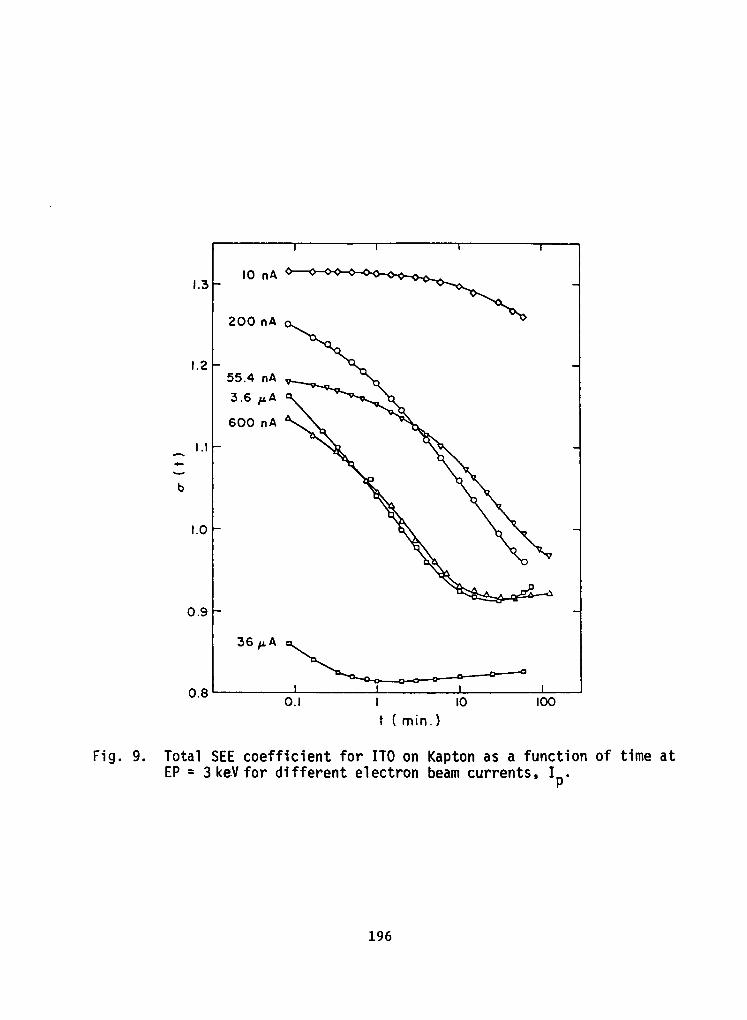
Fig. 9. Total SEE c o e f f i c i e n t f o r IT0 on Kapton as a funct ion of t ime a t EP = 3 k e V f o r d i f f e r e n t e l e c t r o n beam currents, 1
P '

c o s i n e $ Angular dependence of normalized SEE coefficient a of I0 ~ e f 1 on for' several primary beam energies.
5 KeV ,', 1 I I
on FEP
cosine c$
Fig. 11. Angular dependence of normalized SEE coefficient 17 of I0 on .FEP Teflon for several primary beam energies.