section 23. serial peripheral interface (spi)pages.hmc.edu/jspjut/class/f2013/e155/docs/section 23...
TRANSCRIPT

Section 23. Serial Peripheral Interface (SPI)
Serial Peripheral Interface (SPI)
23
HIGHLIGHTSThis section of the manual contains the following topics:
23.1 Introduction.............................................................................................................. 23-223.2 Status and Control Registers ................................................................................... 23-523.3 Modes of Operation ............................................................................................... 23-1323.4 Interrupts................................................................................................................ 23-2923.5 Operation in Power-Saving and Debug Modes ..................................................... 23-3223.6 Effects of Various Resets....................................................................................... 23-3423.7 Peripherals Using SPI Modules............................................................................. 23-3423.8 Design Tips............................................................................................................ 23-3523.9 Related Application Notes ..................................................................................... 23-3623.10 Revision History..................................................................................................... 23-37
© 2009 Microchip Technology Inc. DS61106F-page 23-1
PIC32MX Family Reference Manual
23.1 INTRODUCTIONThe Serial Peripheral Interface (SPI) module is a synchronous serial interface useful forcommunicating with external peripherals and other microcontroller devices. These peripheraldevices may be Serial EEPROMs, shift registers, display drivers, A/D converters, etc. ThePIC32MX family SPI module is compatible with Motorola® SPI and SIOP interfaces.
The following are some of the key features of this module:
• Master and Slave modes support• Four different clock formats• Framed SPI protocol support• Standard and Enhanced Buffering modes (Enhanced buffering mode is not available on all
devices)• User configurable 8-bit, 16-bit, and 32-bit data width• SPI receive and transmitt buffers are FIFO buffers which are 4/8/16 deep in Enhanced
Buffering mode• Separate SPI shift registers for receive and transmit• Programmable interrupt event on every 8-bit, 16-bit, and 32-bit data transfer
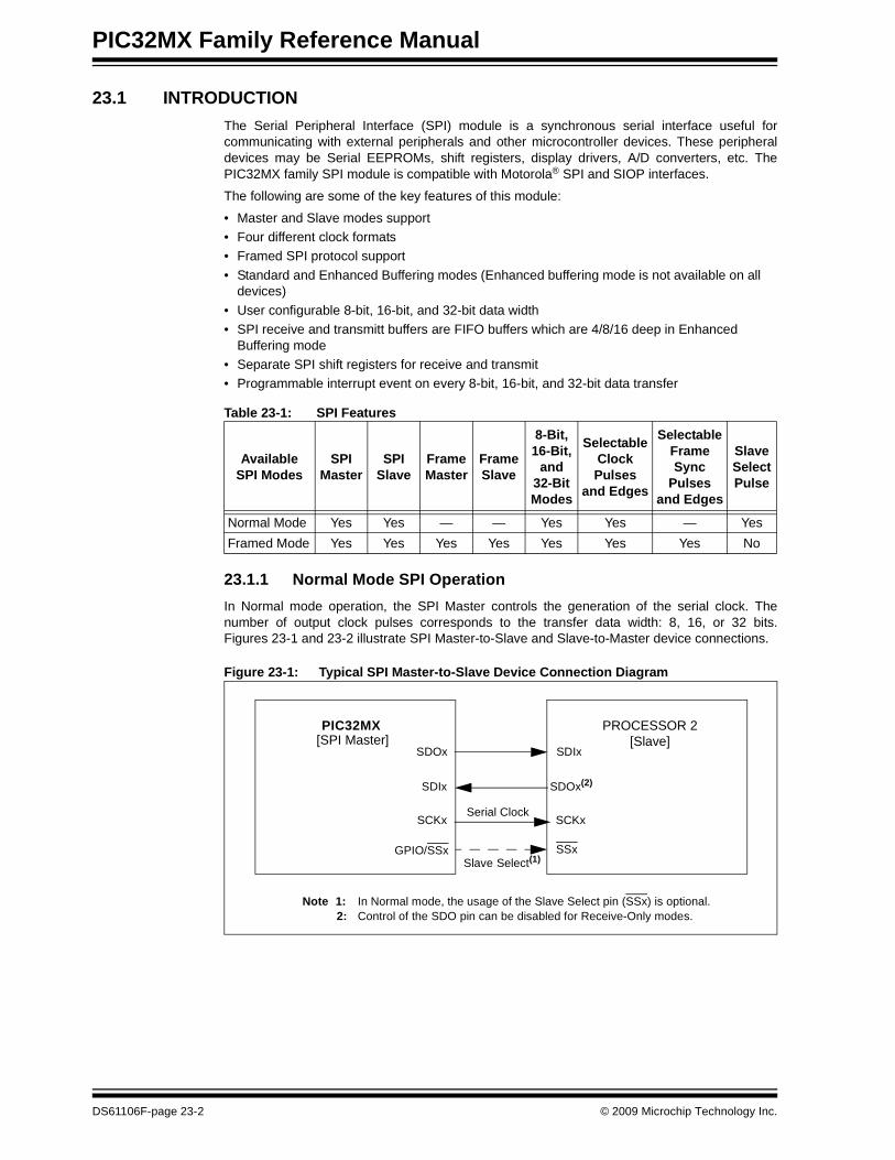
23.1.1 Normal Mode SPI OperationIn Normal mode operation, the SPI Master controls the generation of the serial clock. Thenumber of output clock pulses corresponds to the transfer data width: 8, 16, or 32 bits.Figures 23-1 and 23-2 illustrate SPI Master-to-Slave and Slave-to-Master device connections.
Figure 23-1: Typical SPI Master-to-Slave Device Connection Diagram
Table 23-1: SPI Features
Available SPI Modes
SPI Master
SPI Slave
Frame Master
Frame Slave
8-Bit, 16-Bit,
and 32-Bit Modes
Selectable Clock Pulses
and Edges
Selectable Frame Sync
Pulses and Edges
Slave Select Pulse
Normal Mode Yes Yes — — Yes Yes — YesFramed Mode Yes Yes Yes Yes Yes Yes Yes No
SDOx
SDIx
PIC32MX
Serial Clock
Note 1: In Normal mode, the usage of the Slave Select pin (SSx) is optional.2: Control of the SDO pin can be disabled for Receive-Only modes.
GPIO/SSx
SCKx
Slave Select(1)
SDIx
SDOx(2)
PROCESSOR 2
SSx
SCKx
[SPI Master] [Slave]
DS61106F-page 23-2 © 2009 Microchip Technology Inc.

Section 23. Serial Peripheral Interface (SPI)Serial Peripheral
Interface (SPI)
23
Figure 23-2: Typical SPI Slave-to-Master Device Connection Diagram
23.1.2 Framed Mode SPI OperationIn Framed mode operation, the Frame Master controls the generation of the framesynchronization pulse. The SPI clock is still generated by the SPI Master and is continuouslyrunning. Figures 23-3 and 23-4 illustrate SPI Frame Master and Frame Slave deviceconnections.
Figure 23-3: Typical SPI Master, Frame Master Connection Diagram
Figure 23-4: Typical SPI Master, Frame Slave Connection Diagram
SDOx(2)
SDIx
PIC32MX
Serial Clock
Note 1: In Normal mode, the usage of the Slave Select pin (SSx) is optional.2: The control of the SDO pin can be disabled for Receive-Only modes.
SSx
SCKx
Slave Select(1)
SDIx
SDOx
PROCESSOR 2
SSx/GPIO
SCKx
[SPI Slave] [Master]
SDOx
SDIx
PIC32MX
Serial Clock
Note 1: In Framed SPI mode, the SSx pin is used to transmit/receive the frame synchronization pulse.2: Framed SPI mode requires the use of all four pins (i.e., using the SSx pin is not optional).
SSx
SCKx
Frame Sync.Pulse(1, 2)
SDIx
SDOx
PROCESSOR 2
SSx
SCKx
[SPI Master, Frame Master] [SPI Slave, Frame Slave]
SDOx
SDIx
Serial Clock
Note 1: In Framed SPI mode, the SSx pin is used to transmit/receive the frame synchronization pulse.2: Framed SPI mode requires the use of all four pins (i.e., using the SSx pin is not optional).
SSx
SCKx
Frame Sync.
SDIx
SDOx
SSx
SCKx
PIC32MX[SPI Master, Frame Slave]
PROCESSOR 2[SPI Slave, Frame Master]
Pulse(1, 2)
© 2009 Microchip Technology Inc. DS61106F-page 23-3

PIC32MX Family Reference Manual
Figure 23-5: SPI Module Block Diagram
InternalData Bus
SDIx
SDOx
SSx/FSYNC
SCKx
SPIxSR
bit 0
ShiftControl
EdgeSelect
Enable Master Clock
Baud Rate
Slave Select
Sync Control
ClockControl
Transmit
SPIxRXB(1)
Receive
and Frame
Note 1: The SPIxRXB and SPIxTXB registers are accessed via the SPIxBUF register and are multi-element FIFObuffers in Enhanced Buffer mode. Enhanced Buffer mode is not available on all devices. Refer to the specificdevice data sheet for availability.
Registers share address SPIxBUF
SPIxBUF
Generator PBCLK
WriteRead
SPIxTXB(1)
DS61106F-page 23-4 © 2009 Microchip Technology Inc.

Section 23. Serial Peripheral Interface (SPI)Serial Peripheral
Interface (SPI)
23
23.2 STATUS AND CONTROL REGISTERS
The SPI module consists of the following Special Function Registers (SFRs):
• SPIxCON: SPI Control Register for the Module ‘x’• SPIxSTAT: SPI Status Register for the Module ‘x’• SPIxBUF: SPI Transmit and Receive Buffer Register for the Module ‘x’• SPIxBRG: SPI Baud Rate Generator Register for the Module ‘x’
Each SPI module also has the following associated bits for interrupt control:
• SPIxRXIF, SPIxTXIF, SPIxEIF: Interrupt Flag Status Bits for Receive, Transmit, and Error Events
• SPIxRXIE, SPIxTXIE, SPIxEIE: Interrupt Enable Control Bits for Receive, Transmit, and Error Events
• SPIxIP<2:0>: Interrupt Priority Control bits• SPIxIS<1:0>: Interrupt Subpriority Control bits
Table 23-2 summarizes all SPI-related registers. Corresponding registers appear after thesummary, followed by a detailed description of each register.
Note: Each PIC32MX family device variant may have one or more SPI modules. An ‘x’used in the names of pins, control/Status bits, and registers denotes the particularmodule. Refer to the specific device data sheets for more details.
Table 23-2: SPI SFR Summary
Name AddressOffset
BitRange
Bit31/23/15/7
Bit30/22/14/6
Bit29/21/13/5
Bit28/20/12/4
Bit27/19/11/3
Bit26/18/10/2
Bit25/17/9/1
Bit24/16/8/0
SPIxCON(1,2,3) 0x000 31:24 FRMEN FRMSYNC FRMPOL MSSEN(4) FRMSYPW(4) FRMCNT<2:0>(4)
23:16 — — — — — — SPIFE ENHBUF(4)
15:8 ON FRZ SIDL DISSDO MODE32 MODE16 SMP CKE
7:0 SSEN CKP MSTEN — STXISEL<1:0>(4) SRXISEL<1:0>(4)
SPIxSTAT(2) 0x0010 31:24 — — — RXBUFELM<4:0>(4)
23:16 — — — TXBUFELM<4:0>(4)
15:8 — — — — SPIBUSY — — SPITUR
7:0 SRMT(4) SPIROV SPIRBE(4) — SPITBE — SPITBF(4) SPIRBF
SPIxBUF 0x0020 31:24 DATA<31:24>
23:16 DATA<23:16>
15:8 DATA<15:8>
7:0 DATA<7:0>
SPIxBRG(1,2,3) 0x0030 31:24 — — — — — — — —
23:16 — — — — — — — —
15:8 — — — — — — — BRG<8>
7:0 BRG<7:0>
Legend: — = unimplemented, read as ‘0’. Address offset values are shown in hexadecimal.Note 1: This register has an associated Clear register at an offset of 0x4 bytes. These registers have the same name with CLR appended to the
end of the register name (e.g., SPIxCONCLR). Writing a ‘1’ to any bit position in the Clear register will clear valid bits in the associated reg-ister. Reads from the Clear register should be ignored.
2: This register has an associated Set register at an offset of 0x8 bytes. These registers have the same name with SET appended to the end of the register name (e.g., SPIxCONSET). Writing a ‘1’ to any bit position in the Set register will set valid bits in the associated register. Reads from the Set register should be ignored.
3: This register has an associated Invert register at an offset of 0xC bytes. These registers have the same name with INV appended to the end of the register name (e.g., SPIxCONINV). Writing a ‘1’ to any bit position in the Invert register will invert valid bits in the associated register. Reads from the Invert register should be ignored.
4: This bit is not available on all devices. Refer to the specific device data sheet for details.
© 2009 Microchip Technology Inc. DS61106F-page 23-5

PIC32MX Family Reference Manual
Register 23-1: SPIxCON: SPI Control Register(1,2,3) R/W-0 R/W-0 R/W-0 R/W-0 R/W-0 R/W-0 R/W-0 R/W-0
FRMEN FRMSYNC FRMPOL MSSEN(4) FRMSYPW(4) FRMCNT<2:0>(4)
bit 31 bit 24
r-x r-x r-x r-x r-x r-x R/W-0 R/W-0— — — — — — SPIFE ENHBUF(4)
bit 23 bit 16
R/W-0 R/W-0 R/W-0 R/W-0 R/W-0 R/W-0 R/W-0 R/W-0ON FRZ SIDL DISSDO MODE32 MODE16 SMP CKE
bit 15 bit 8
R/W-0 R/W-0 R/W-0 r-x R/W-0 R/W-0 R/W-0 R/W-0SSEN CKP MSTEN — STXISEL<1:0>(4) SRXISEL<1:0>(4)
bit 7 bit 0
Legend:R = Readable bit W = Writable bit P = Programmable bit r = Reserved bitU = Unimplemented bit -n = Bit Value at POR: (‘0’, ‘1’, x = Unknown)
bit 31 FRMEN: Framed SPI Support bit1 = Framed SPI support is enabled (SSx pin used as FSYNC input/output)0 = Framed SPI support is disabled
bit 30 FRMSYNC: Frame Sync Pulse Direction Control on SSx pin bit (Framed SPI mode only)1 = Frame sync pulse input (Slave mode)0 = Frame sync pulse output (Master mode)
bit 29 FRMPOL: Frame Sync Polarity bit (Framed SPI mode only)1 = Frame pulse is active-high0 = Frame pulse is active-low
bit 28 MSSEN: Master Mode Slave Select Enable bit(4)
1 = Slave select SPI support enabled. The SS pin is automatically driven during transmission in Mastermode. Polarity is determined by the FRMPOL bit.
0 = Slave select SPI support is disabled.bit 27 FRMSYPW: Frame Sync Pulse Width bit(4)
1 = Frame sync pulse is one character wide0 = Frame sync pulse is one clock wide
Note 1: This register has an associated Clear register (SPIxCONCLR) at an offset of 0x4 bytes. Writing a ‘1’ to anybit position in the Clear register will clear valid bits in the associated register. Reads from the Clear registershould be ignored.
2: This register has an associated Set register (SPIxCONSET) at an offset of 0x8 bytes. Writing a ‘1’ to anybit position in the Set register will set valid bits in the associated register. Reads from the Set registershould be ignored.
3: This register has an associated Invert register (SPIxCONINV) at an offset of 0xC bytes. Writing a ‘1’ to anybit position in the Invert register will invert valid bits in the associated register. Reads from the Invert registershould be ignored.
4: These bits are not available on all devices. Refer to the specific device data sheet for availability.
DS61106F-page 23-6 © 2009 Microchip Technology Inc.

Section 23. Serial Peripheral Interface (SPI)Serial Peripheral
Interface (SPI)
23
bit 26-24 FRMCNT<2:0>: Frame Sync Pulse Counter bits. Controls the number of data characters transmitted per pulse.(4)
111 = Reserved; do not use110 = Reserved; do not use101 = Generate a frame sync pulse on every 32 data characters100 = Generate a frame sync pulse on every 16 data characters011 = Generate a frame sync pulse on every 8 data characters010 = Generate a frame sync pulse on every 4 data characters001 = Generate a frame sync pulse on every 2 data characters000 = Generate a frame sync pulse on every data character
Note: This bit is only valid in FRAMED_SYNC mode.bit 23-18 Reserved: Write ‘0’; ignore readbit 17 SPIFE: Frame Sync Pulse Edge Select bit (Framed SPI mode only)
1 = Frame synchronization pulse coincides with the first bit clock0 = Frame synchronization pulse precedes the first bit clock
bit 16 ENHBUF: Enhanced Buffer Enable bit(4)
1 = Enhanced Buffer mode is enabled0 = Enhanced Buffer mode is disabled
Note: This bit can only be written when the ON bit = 0.bit 15 ON: SPI Peripheral On bit
1 = SPI Peripheral is enabled0 = SPI Peripheral is disabled
Note: When using the 1:1 PBCLK divisor, the user’s software should not read or write theperipheral’s SFRs in the SYSCLK cycle immediately following the instruction that clears themodule’s ON bit.
bit 14 FRZ: Freeze in Debug Exception Mode bit1 = Freeze operation when CPU enters Debug Exception mode0 = Continue operation when CPU enters Debug Exception mode
Note: FRZ is writable in Debug Exception mode only, it is forced to ‘0’ in Normal mode.bit 13 SIDL: Stop in Idle Mode bit
1 = Discontinue operation when CPU enters in Idle mode0 = Continue operation in Idle mode
bit 12 DISSDO: Disable SDOx pin bit1 = SDOx pin is not used by the module. Pin is controlled by associated PORT register0 = SDOx pin is controlled by the module
bit 11-10 MODE<32,16>: 32/16-Bit Communication Select bits1x = 32-bit data width01 = 16-bit data width00 = 8-bit data width
Register 23-1: SPIxCON: SPI Control Register(1,2,3) (Continued)
Note 1: This register has an associated Clear register (SPIxCONCLR) at an offset of 0x4 bytes. Writing a ‘1’ to anybit position in the Clear register will clear valid bits in the associated register. Reads from the Clear registershould be ignored.
2: This register has an associated Set register (SPIxCONSET) at an offset of 0x8 bytes. Writing a ‘1’ to anybit position in the Set register will set valid bits in the associated register. Reads from the Set registershould be ignored.
3: This register has an associated Invert register (SPIxCONINV) at an offset of 0xC bytes. Writing a ‘1’ to anybit position in the Invert register will invert valid bits in the associated register. Reads from the Invert registershould be ignored.
4: These bits are not available on all devices. Refer to the specific device data sheet for availability.
© 2009 Microchip Technology Inc. DS61106F-page 23-7

PIC32MX Family Reference Manual
bit 9 SMP: SPI Data Input Sample Phase bitMaster mode (MSTEN = 1):1 = Input data sampled at end of data output time0 = Input data sampled at middle of data output timeSlave mode (MSTEN = 0):SMP value is ignored when SPI is used in Slave mode. The module always uses SMP = 0.
bit 8 CKE: SPI Clock Edge Select bit1 = Serial output data changes on transition from active clock state to Idle clock state (see CKP bit)0 = Serial output data changes on transition from Idle clock state to active clock state (see CKP bit)
Note: The CKE bit is not used in the Framed SPI mode. The user should program this bit to ‘0’for the Framed SPI mode (FRMEN = 1).
bit 7 SSEN: Slave Select Enable (Slave mode) bit1 = SSx pin used for Slave mode0 = SSx pin not used for Slave mode, pin controlled by port function.
bit 6 CKP: Clock Polarity Select bit1 = Idle state for clock is a high level; active state is a low level0 = Idle state for clock is a low level; active state is a high level
bit 5 MSTEN: Master Mode Enable bit1 = Master mode0 = Slave mode
bit 4 Reserved: Write ‘0’; ignore readbit 3-2 STXISEL<1:0>: SPI Transmit Buffer Empty Interrupt Mode bits(4)
11 = SPI_TBE_EVENT is set when the buffer is not full (has one or more empty elements)10 = SPI_TBE_EVENT is set when the buffer is empty by one-half or more01 = SPI_TBE_EVENT is set when the buffer is completely empty00 = SPI_TBE_EVENT is set when the last transfer is shifted out of SPISR and transmit operations
are completebit 1-0 RTXISEL<1:0>: SPI Receive Buffer Full Interrupt Mode bits(4)
11 = SPI_RBF_EVENT is set when the buffer is full10 = SPI_RBF_EVENT is set when the buffer is full by one-half or more01 = SPI_RBF_EVENT is set when the buffer is not empty00 = SPI_RBF_EVENT is set when the last word in the receive buffer is read (i.e., buffer is empty)
Register 23-1: SPIxCON: SPI Control Register(1,2,3) (Continued)
Note 1: This register has an associated Clear register (SPIxCONCLR) at an offset of 0x4 bytes. Writing a ‘1’ to anybit position in the Clear register will clear valid bits in the associated register. Reads from the Clear registershould be ignored.
2: This register has an associated Set register (SPIxCONSET) at an offset of 0x8 bytes. Writing a ‘1’ to anybit position in the Set register will set valid bits in the associated register. Reads from the Set registershould be ignored.
3: This register has an associated Invert register (SPIxCONINV) at an offset of 0xC bytes. Writing a ‘1’ to anybit position in the Invert register will invert valid bits in the associated register. Reads from the Invert registershould be ignored.
4: These bits are not available on all devices. Refer to the specific device data sheet for availability.
DS61106F-page 23-8 © 2009 Microchip Technology Inc.

Section 23. Serial Peripheral Interface (SPI)Serial Peripheral
Interface (SPI)
23
Register 23-2: SPIxSTAT: SPI Status Register(1)
r-x r-x r-x R-0 R-0 R-0 R-0 R-0— — — RXBUFELM<4:0>(2)
bit 31 bit 24
r-x r-x r-x R-0 R-0 R-0 R-0 R-0— — — TXBUFELM<4:0>(2)
bit 23 bit 16
r-x r-x r-x r-x R-0 r-x r-x R-0— — — — SPIBUSY — — SPITUR(2)
bit 15 bit 8
R-0 R/W-0 R-0 r-x R-1 r-x R-0 R-0SRMT(2) SPIROV SPIRBE(2) — SPITBE — SPITBF(2) SPIRBF
bit 7 bit 0
Legend:R = Readable bit W = Writable bit P = Programmable bit r = Reserved bitU = Unimplemented bit -n = Bit Value at POR: (‘0’, ‘1’, x = Unknown)
bit 31-29 Reserved: Write ‘0’; ignore readbit 28-24 RXBUFELM<4:0>: Receive Buffer Element Count bits (valid only when ENHBUF = 1)(2)
Reflects the value mod (SWPTR - CRPTR) taking into account empty and full conditions.bit 23-21 Reserved: Write ‘0’; ignore readbit 20-16 TXBUFELM<4:0>: Transmit Buffer Element Count bits (valid only when ENHBUF = 1)(2)
Reflects the value mod (CWPTR - SRPTR) taking into account empty and full conditions.bit 15-12 Reserved: Write ‘0’; ignore readbit 11 SPIBUSY: SPI Activity Status bit
1 = SPI peripheral is currently busy with some transactions0 = SPI peripheral is currently idle
bit 10-9 Reserved: Write ‘0’; ignore readbit 8 SPITUR: Transmit Under Run bit(2)
1 = Transmit buffer has encountered an underrun condition0 = Transmit buffer has no underrun conditionThis bit is only valid in Framed Sync mode; the underrun condition must be cleared bydisabling/re-enabling the module.
bit 7 SRMT: Shift Register Empty bit (valid only when ENHBUF = 1)(2)
1 = When RX_READY = 10 = When RX_READY = 0
bit 6 SPIROV: Receive Overflow Flag bit1 = A new data is completely received and discarded. The user software has not read the previous
data in the SPIxBUF register.0 = No overflow has occurredThis bit is set in hardware; can only be cleared (= 0) in software.
Note 1: This register has an associated Clear register (SPIxSTATCLR) at an offset of 0x4 bytes. Writing a ‘1’ toany bit position in the Clear register will clear valid bits in the associated register. Reads from the Clearregister should be ignored.
2: These bits are not available on all devices. Refer to the specific device data sheet for availability.
© 2009 Microchip Technology Inc. DS61106F-page 23-9

PIC32MX Family Reference Manual
bit 5 SPIRBE: RX FIFO Empty bit (valid only when ENHBUF = 1)1 = RX FIFO is empty (CRPTR = SWPTR)0 = RX FIFO is not empty (CRPTR ≠ SWPTR)
bit 4 Reserved: Write ‘0’; ignore readbit 3 SPITBE: SPI Transmit Buffer Empty Status bit(2)
1 = Transmit buffer, SPIxTXB is empty0 = Transmit buffer, SPIxTXB is not emptyAutomatically set in hardware when SPI transfers data from SPIxTXB to SPIxSR.Automatically cleared in hardware when SPIxBUF is written to, loading SPIxTXB.
bit 2 Reserved: Write ‘0’; ignore readbit 1 SPITBF: SPI Transmit Buffer Full Status bit(2)
1 = Transmit not yet started, SPITXB is full0 = Transmit buffer is not fullStandard Buffer Mode:Automatically set in hardware when the core writes to the SPIBUF location, loading SPITXB.Automatically cleared in hardware when the SPI module transfers data from SPITXB to SPISR.Enhanced Buffer Mode:Set when CWPTR + 1 = SRPTR; cleared otherwise
bit 0 SPIRBF: SPI Receive Buffer Full Status bit1 = Receive buffer, SPIxRXB is full0 = Receive buffer, SPIxRXB is not fullStandard Buffer Mode:Automatically set in hardware when the SPI module transfers data from SPIxSR to SPIxRXB.Automatically cleared in hardware when SPIxBUF is read from, reading SPIxRXB.Enhanced Buffer Mode:Set when SWPTR + 1 = CRPTR; cleared otherwise
Register 23-2: SPIxSTAT: SPI Status Register(1)
Note 1: This register has an associated Clear register (SPIxSTATCLR) at an offset of 0x4 bytes. Writing a ‘1’ toany bit position in the Clear register will clear valid bits in the associated register. Reads from the Clearregister should be ignored.
2: These bits are not available on all devices. Refer to the specific device data sheet for availability.
DS61106F-page 23-10 © 2009 Microchip Technology Inc.

Section 23. Serial Peripheral Interface (SPI)Serial Peripheral
Interface (SPI)
23
Register 23-3: SPIxBUF: SPI Buffer RegisterR/W-0 R/W-0 R/W-0 R/W-0 R/W-0 R/W-0 R/W-0 R/W-0
DATA<31:24>bit 31 bit 24
R/W-0 R/W-0 R/W-0 R/W-0 R/W-0 R/W-0 R/W-0 R/W-0DATA<23:16>
bit 23 bit 16
R/W-0 R/W-0 R/W-0 R/W-0 R/W-0 R/W-0 R/W-0 R/W-0DATA<15:8>
bit 15 bit 8
R/W-0 R/W-0 R/W-0 R/W-0 R/W-0 R/W-0 R/W-0 R/W-0DATA<7:0>
bit 7 bit 0
Legend:R = Readable bit W = Writable bit P = Programmable bit r = Reserved bitU = Unimplemented bit -n = Bit Value at POR: (‘0’, ‘1’, x = Unknown)
bit 31-0 DATA<31:0>: SPI Transmit/Receive Buffer registerServes as a memory-mapped value of Transmit (SPIxTXB) and Receive (SPIxSR) registers.
When 32-Bit Data mode is enabled (MODE<32,16> (SPIxCON<11:10>) = 1x):
All 32-bits (SPIxBUF<31:0>) of this register are used to form a 32-bit character.
When 16-Bit Data mode is enabled (MODE<32,16> (SPIxCON<11:10>) = 01):
Only lower 16-bits (SPIxBUF<15:0>) of this register are used to form the 16-bit character.
When 8-Bit Data mode is enabled (MODE<32,16> (SPIxCON<11:10>) = 00):
Only lower 8-bits (SPIxBUF<7:0>) of this register are used to form the 8-bit character.
© 2009 Microchip Technology Inc. DS61106F-page 23-11

PIC32MX Family Reference Manual
Register 23-4: SPIXBRG: SPI Baud Rate Register(1,2,3)
r-x r-x r-x r-x r-x r-x r-x r-x— — — — — — — —
bit 31 bit 24
r-x r-x r-x r-x r-x r-x r-x r-x— — — — — — — —
bit 23 bit 16
r-x r-x r-x r-x r-x r-x r-x R/W-0— — — — — — — BRG<8>
bit 15 bit 8
R/W-0 R/W-0 R/W-0 R/W-0 R/W-0 R/W-0 R/W-0 R/W-0BRG<7:0>
bit 7 bit 0
Legend:R = Readable bit W = Writable bit P = Programmable bit r = Reserved bitU = Unimplemented bit -n = Bit Value at POR: (‘0’, ‘1’, x = Unknown)
bit 31-9 Reserved: Write ‘0’; ignore readbit 8-0 BRG<8:0>: Baud Rate Divisor bits
Note 1: This register has an associated Clear register (SPIxBRGCLR) at an offset of 0x4 bytes. Writing a ‘1’ to anybit position in the Clear register will clear valid bits in the associated register. Reads from the Clear registershould be ignored.
2: This register has an associated Set register (SPIxBRGSET) at an offset of 0x8 bytes. Writing a ‘1’ to anybit position in the Set register will set valid bits in the associated register. Reads from the Set registershould be ignored.
3: This register has an associated Invert register (SPIxBRGINV) at an offset of 0xC bytes. Writing a ‘1’ to anybit position in the Invert register will invert valid bits in the associated register. Reads from the Invertregister should be ignored.
DS61106F-page 23-12 © 2009 Microchip Technology Inc.

Section 23. Serial Peripheral Interface (SPI)Serial Peripheral
Interface (SPI)
23
23.3 MODES OF OPERATIONThe SPI module offers the following operating modes:
• 8-Bit, 16-Bit, and 32-bit data transmission modes• 8-Bit, 16-Bit, and 32-bit data reception modes• Master and Slave modes• Framed SPI modes
23.3.1 8-Bit, 16-Bit, and 32-Bit OperationThe PIC32MX SPI module allows three types of data widths when transmitting and receiving dataover an SPI bus. The selection of data width determines the minimum length of SPI data. Forexample, when the selected data width is 32, all transmission and receptions are performed in32-bit values. All reads and writes from the CPU are also performed in 32-bit values. Accordingly,the application software should select the appropriate data width to maximize its data throughput.
Two control bits, MODE32 and MODE16 (SPIxCON<11:10>), define the mode of operation. Tochange the mode of operation on the fly, the SPI module must be idle (i.e., not performing anytransactions). If the SPI module is switched off (SPIxCON<15> = 0), the new mode will beavailable when the module is again switched on.
Additionally, the following items should be noted in this context:
• The MODE32 and MODE16 bits should not be changed when a transaction is in progress. • The first bit to be shifted out from SPIxSR varies with the selected mode of operation:
- 8-Bit mode, bit 7 - 16-Bit mode, bit 15- 32-Bit mode, bit 31
• In each mode, data is shifted into bit 0 of the SPIxSR.• The number of clock pulses at the SCKx pin are also dependent on the selected mode of
operation:- 8-Bit mode, 8 clocks- 16-Bit mode, 16 clocks- 32-Bit mode, 32 clocks
23.3.2 Buffer ModesThere are two SPI buffering modes: Standard and Enhanced.
23.3.2.1 STANDARD BUFFER MODE
The SPI Data Receive/Transmit Buffer (SPIxBUF) register is actually two separate internalregisters: the Transmit Buffer (SPIxTXB) and the Receive Buffer (SPIxRXB). These twounidirectional registers share the SFR address of SPIxBUF.
When a complete byte/word is received, it is transferred from SPISR to SPIRXB and the SPIRBFflag is set. If the software reads the SPIxBUF buffer, the SPIRBF bit is cleared.
As the software writes to SPIxBUF, the data is loaded into the SPITXB bit and the SPITBF bit isset by hardware. As the data is transmitted out of SPISR, the SPITBF flag is cleared.
The SPI module double-buffers transmit/receive operations and allow continuous data transfersin the background. Transmission and reception occur simultaneously in the SPISR bit.
Note: Enhanced Buffer mode is not available on all devices. Refer to the specific devicedata sheet for details.
© 2009 Microchip Technology Inc. DS61106F-page 23-13

PIC32MX Family Reference Manual
23.3.2.2 ENHANCED BUFFER MODE
The Enhanced Buffer Enable (ENHBUF) bit in the SPI Control (SPIxCON<16>) register can beset to enable the Enhanced Buffer mode.
In Enhanced Buffer mode, multi-element FIFO buffers are used for the transmit buffer (SPIxTXB)and the receive buffer (SPIxRXB). SPIxBUF provides access to both the receive and transmitFIFOs and the data transmission and reception in the SPISR buffer in this mode is identical tothat in Standard Buffer mode. The FIFO depth depends on the data width chosen by theWord/Half-Word Byte Communication Select (MODE<32,16>) bits in the SPI Control(SPIxCON<11:10>) register. If the MODE field selects 32-bit data lengths, the FIFO is 4 deep, ifMODE selects 16-bit data lengths, the FIFO is 8 deep, or if MODE selects 8-bit data lengths theFIFO is 16 deep.
The SPITBF status bit is set when all of the elements in the transmit FIFO buffer are full and iscleared if one or more of those elements are empty. The SPIRBF status bit is set when all of theelements in the receive FIFO buffer are full and is cleared if the SPIxBUF buffer is read by thesoftware.
The SPITBE status bit is set if all the elements in the transmit FIFO buffer are empty and iscleared otherwise. The SPIRBE bit is set if all of the elements in the receive FIFO buffer areempty and is cleared otherwise. The Shift Register Empty (SRMT) bit is valid only in EnhancedBuffer mode and is set when the shift register is empty and cleared otherwise.
There is no underrun or overflow protection against reading an empty receive FIFO element orwriting a full transmit FIFO element. However, the SPISR bit provides Transmit Underrun(SPITUR) and Receive Overflow (SPIROV) status bit, which can be monitored along with theother status bits.
The Receive Buffer Element Count (RXBUFELM<4:0>) bits in the SPI Status(SPIxSTAT<28:24>) register indicate the number of unread elements in the receive FIFO. TheTransmit Buffer Element Count (TXBUFELM<4:0>) bits in the SPI Status (SPIxSTAT<20:16>)register indicate the number of elements not transmitted in the transmit FIFO.
DS61106F-page 23-14 © 2009 Microchip Technology Inc.

Section 23. Serial Peripheral Interface (SPI)Serial Peripheral
Interface (SPI)
23
23.3.3 Master and Slave Modes
Figure 23-6: SPI Master/Slave Connection Diagram
23.3.3.1 MASTER MODE OPERATION
Perform the following steps to set up the SPI module for the Master mode operation:
1. Disable the SPI interrupts in the respective IEC0/1 register.2. Stop and reset the SPI module by clearing the ON bit.3. Clear the receive buffer.4. Clear the ENHBUF bit (SPIxCON<16>) if using Standard Buffer mode or set the bit if using
Enhanced Buffer mode.5. If SPI interrupts are not going to be used, skip this step and continue to step 5. Otherwise
the following additional steps are performed:a) Clear the SPIx interrupt flags/events in the respective IFS0/1 register.b) Set the SPIx interrupt enable bits in the respective IEC0/1 register.c) Write the SPIx interrupt priority and subpriority bits in the respective IPC5/7 register.
6. Write the Baud Rate register, SPIxBRG.7. Clear the SPIROV bit (SPIxSTAT<6>).8. Write the desired settings to the SPIxCON register with MSTEN (SPIxCON<5>) = 1. 9. Enable SPI operation by setting the ON bit (SPIxCON<15>).10. Write the data to be transmitted to the SPIxBUF register. Transmission (and reception) will
start as soon as data is written to the SPIxBUF register.
Serial Receive Buffer(SPIxRXB)
Shift Register(SPIxSR)
LSBMSB
SDIx
SDOx
PROCESSOR 2
SCKx
SSx(1)
Serial Transmit Buffer(SPIxTXB)
Serial Receive Buffer(SPIxRXB)(2)
Shift Register(SPIxSR)
MSB LSB
SDOx
SDIx
PIC32MX
Serial Clock
SSEN (SPIxCON<7>) = 1 andMSTEN (SPIxCON<5>) = 0
Note 1: Using the SSx pin in Slave mode of operation is optional.2: User must write transmit data to SPIxBUF and read received data from SPIxBUF. The SPIxTXB and SPIxRXB
registers are memory mapped to SPIxBUF.
GPIO/SSx
SCKx
Serial Transmit Buffer(SPIxTXB)(2)
MSTEN (SPIxCON<5>) = 1
SPI Buffer(SPIxBUF)
SPI Buffer(SPIxBUF)
[SPI Master] [SPI Slave]
© 2009 Microchip Technology Inc. DS61106F-page 23-15

PIC32MX Family Reference Manual
In Master mode, the PBCLK is divided and then used as the serial clock. The division is basedon the settings in the SPIxBRG register. The serial clock is output via the SCKx pin to slavedevices. Clock pulses are only generated when there is data to be transmitted; except when inFramed mode, when clock is generated continuously. For further information, refer to Section23.3.7 “SPI Master Mode Clock Frequency”.
The Master Mode Slave Select Enable (MSSEN) bit in the SPI Control (SPIxCON<28>) registercan be set to automatically drive the slave select signal (SS) in Master mode. Clearing this bitdisabled the slave select signal support in Master mode. The FRMPOL (SPIxCON<29>) bitdetermines the polarity for the slave select signal in Master mode.
Bits CKP (SPIxCON<6>) and CKE (SPIxCON<8>) determine on which edge of the clock datatransmission occurs.
Both data to be transmitted and data that is received are written to, or read from, the SPIxBUFregister, respectively.
The following progression describes the SPI module operation in Master mode:
1. Once the module is set up for Master mode operation and enabled, data to be transmittedis written to SPIxBUF register. The SPITBE (SPIxSTAT<3>) bit is cleared.
2. The contents of SPIxTXB are moved to the shift register SPIxSR (see Figure 23-6), andthe SPITBE bit is set by the module.
3. A series of 8/16/32 clock pulses shifts 8/16/32 bits of transmit data from SPIxSR to theSDOx pin and simultaneously shifts the data at the SDIx pin into SPIxSR.
4. When the transfer is complete, the following events will occur:a) The interrupt flag bit SPIxRXIF is set. SPI interrupts can be enabled by setting the
interrupt enable bit SPIxRXIE. The SPIxRXIF flag is not cleared automatically by thehardware.
b) Also, when the ongoing transmit and receive operation is completed, the contents ofSPIxSR are moved to SPIxRXB.
c) The SPIRBF bit (SPIxSTAT<0>) is set by the module, indicating that the receivebuffer is full. Once SPIxBUF is read by the user code, the hardware clears theSPIRBF bit. In Enhanced Buffer mode the SPIRBE (SPIxSTAT<5>) bit is set whenthe SPIxRXB FIFO buffer is completely empty and cleared when not empty.
5. If the SPIRBF bit is set (the receive buffer is full) when the SPI module needs to transferdata from SPIxSR to SPIxRXB, the module will set the SPIROV bit (SPIxSTAT<6>)indicating an overflow condition.
6. Data to be transmitted can be written to SPIxBUF by the user software at any time, if theSPITBE (SPIxSTAT<3>) bit is set. The write can occur while SPIxSR is shifting out thepreviously written data, allowing continuous transmission. In Enhanced Buffer mode theSPITBF (SPIxSTAT<1>) bit is set when the SPIxTXB FIFO buffer is completely full andclear when it is not full.
Note: The SPI device must be turned off prior to changing the mode from Slave to Master.When using the Slave Select mode, the SSx or another GPIO pin is used to controlthe slave’s SSx input. The pin must be controlled in software.
Note: The MSSEN bit is not available on all devices. Refer to the specific device datasheet for details.
Note: The user must turn off the SPI device prior to changing the CKE or CKP bits.Otherwise, the behavior of the device is not guaranteed.
Note: The SPIxSR register cannot be written to directly by the user. All writes to theSPIxSR register are performed through the SPIxBUF register.
DS61106F-page 23-16 © 2009 Microchip Technology Inc.
Section 23. Serial Peripheral Interface (SPI)Serial Peripheral
Interface (SPI)
23
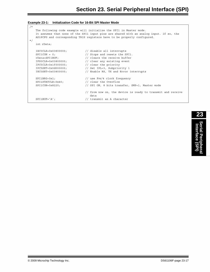
Example 23-1: Initialization Code for 16-Bit SPI Master Mode/*
The following code example will initialize the SPI1 in Master mode.It assumes that none of the SPI1 input pins are shared with an analog input. If so, the AD1PCFG and corresponding TRIS registers have to be properly configured.
*/int rData;
IEC0CLR=0x03800000; // disable all interruptsSPI1CON = 0; // Stops and resets the SPI1. rData=SPI1BUF; // clears the receive bufferIFS0CLR=0x03800000; // clear any existing eventIPC5CLR=0x1f000000; // clear the priorityIPC5SET=0x0d000000; // Set IPL=3, Subpriority 1IEC0SET=0x03800000; // Enable RX, TX and Error interrupts
SPI1BRG=0x1; // use FPB/4 clock frequencySPI1STATCLR=0x40; // clear the OverflowSPI1CON=0x8220; // SPI ON, 8 bits transfer, SMP=1, Master mode
// from now on, the device is ready to transmit and receivedata
SPI1BUF=’A’; // transmit an A character
© 2009 Microchip Technology Inc. DS61106F-page 23-17

PIC32MX Family Reference Manual
Figure 23-7: SPI Master Mode Operation in 8-Bit Mode (MODE32 = 0, MODE16 = 0)
SCKx(CKP = 0
SCKx(CKP = 1
SCKx(CKP = 0
SCKx(CKP = 1
4 Clock modes
InputSample(2)
InputSample
SDIx(2)
bit 7 bit 0
SDOx bit 7 bit 6 bit 5 bit 4 bit 3 bit 2 bit 1 bit 0
bit 7 bit 0SDIx
SPIxRXIF
(SMP = 1)
(SMP = 0)
(SMP = 1)
CKE = 1)
CKE = 0)
CKE = 0)
CKE = 0)
(SMP = 0)
User writesto SPIxBUF
SDOx bit 7 bit 6 bit 5 bit 4 bit 3 bit 2 bit 1 bit 0
(CKE = 0)
(CKE = 1)
Approximately 2 SYSCLK latency to setSPIxRXIF flag bit
Note 1: Four SPI Clock modes are shown here to demonstrate the functionality of bits CKP (SPIxCON<6>) and CKE(SPIxCON<8>). Only one of the four modes can be chosen for operation.
2: The SDI and input samples shown here for two different values of the SMP bit (SPIxCON<9>) are strictly for dem-onstration purposes. Only one of the two configurations of the SMP bit can be chosen during operation.
3: If there are no pending transmissions, SPIxTXB is transferred to SPIxSR as soon as the user writes to SPIxBUF.4: Operation for 8-bit mode shown. 16-bit and 32-bit modes are similar.
SPIxSR movedinto SPIxRXB
User reads SPIxBUF
(clock outputat the SCKx pin in Master mode)(1)
(SPIxSTAT<0>)
SPITBE
SPIxTXB to SPIxSR(3)User writes new dataduring transmission
SPIRBF
Two modesavailable forSMP controlbit(4)
DS61106F-page 23-18 © 2009 Microchip Technology Inc.
Section 23. Serial Peripheral Interface (SPI)Serial Peripheral
Interface (SPI)
23
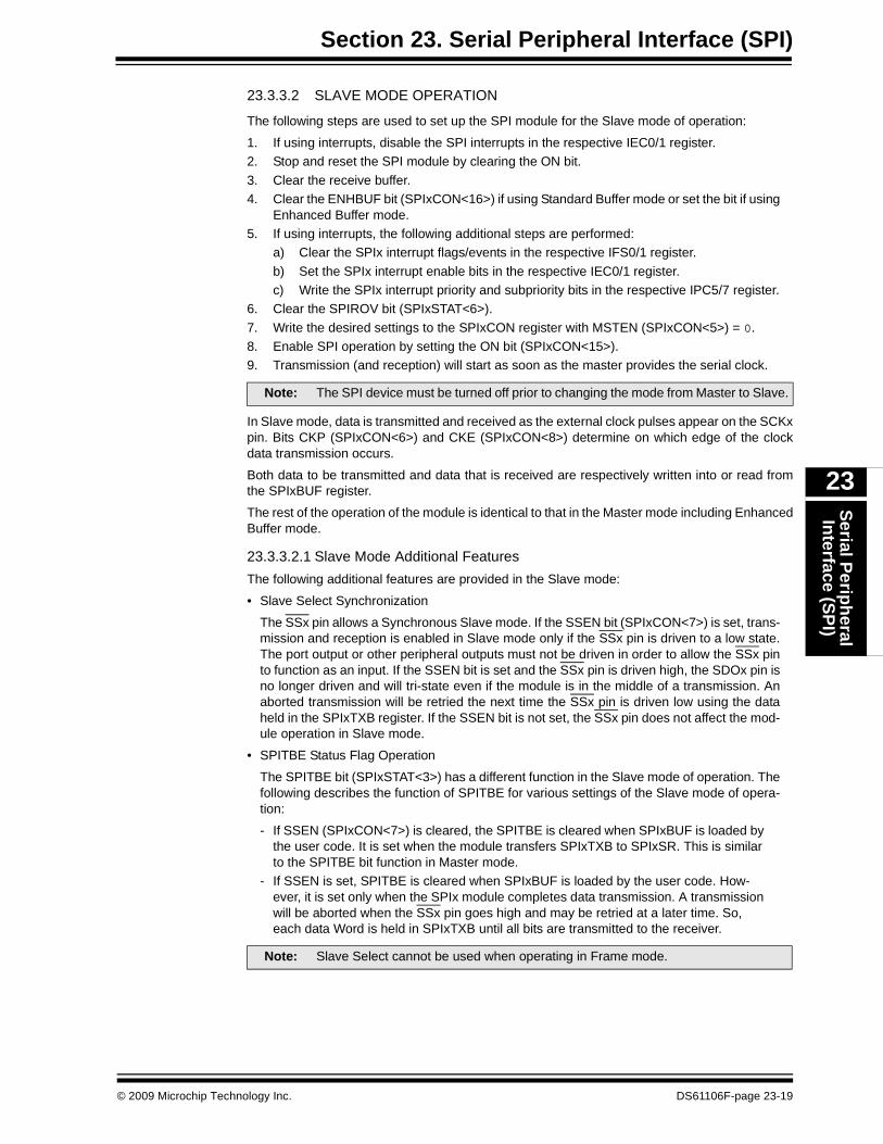
23.3.3.2 SLAVE MODE OPERATION
The following steps are used to set up the SPI module for the Slave mode of operation:
1. If using interrupts, disable the SPI interrupts in the respective IEC0/1 register.2. Stop and reset the SPI module by clearing the ON bit.3. Clear the receive buffer.4. Clear the ENHBUF bit (SPIxCON<16>) if using Standard Buffer mode or set the bit if using
Enhanced Buffer mode.5. If using interrupts, the following additional steps are performed:
a) Clear the SPIx interrupt flags/events in the respective IFS0/1 register.b) Set the SPIx interrupt enable bits in the respective IEC0/1 register.c) Write the SPIx interrupt priority and subpriority bits in the respective IPC5/7 register.
6. Clear the SPIROV bit (SPIxSTAT<6>).7. Write the desired settings to the SPIxCON register with MSTEN (SPIxCON<5>) = 0. 8. Enable SPI operation by setting the ON bit (SPIxCON<15>).9. Transmission (and reception) will start as soon as the master provides the serial clock.
In Slave mode, data is transmitted and received as the external clock pulses appear on the SCKxpin. Bits CKP (SPIxCON<6>) and CKE (SPIxCON<8>) determine on which edge of the clockdata transmission occurs.
Both data to be transmitted and data that is received are respectively written into or read fromthe SPIxBUF register.
The rest of the operation of the module is identical to that in the Master mode including EnhancedBuffer mode.
23.3.3.2.1 Slave Mode Additional FeaturesThe following additional features are provided in the Slave mode:
• Slave Select Synchronization
The SSx pin allows a Synchronous Slave mode. If the SSEN bit (SPIxCON<7>) is set, trans-mission and reception is enabled in Slave mode only if the SSx pin is driven to a low state.The port output or other peripheral outputs must not be driven in order to allow the SSx pinto function as an input. If the SSEN bit is set and the SSx pin is driven high, the SDOx pin isno longer driven and will tri-state even if the module is in the middle of a transmission. Anaborted transmission will be retried the next time the SSx pin is driven low using the dataheld in the SPIxTXB register. If the SSEN bit is not set, the SSx pin does not affect the mod-ule operation in Slave mode.
• SPITBE Status Flag Operation
The SPITBE bit (SPIxSTAT<3>) has a different function in the Slave mode of operation. Thefollowing describes the function of SPITBE for various settings of the Slave mode of opera-tion:
- If SSEN (SPIxCON<7>) is cleared, the SPITBE is cleared when SPIxBUF is loaded by the user code. It is set when the module transfers SPIxTXB to SPIxSR. This is similar to the SPITBE bit function in Master mode.
- If SSEN is set, SPITBE is cleared when SPIxBUF is loaded by the user code. How-ever, it is set only when the SPIx module completes data transmission. A transmission will be aborted when the SSx pin goes high and may be retried at a later time. So, each data Word is held in SPIxTXB until all bits are transmitted to the receiver.
Note: The SPI device must be turned off prior to changing the mode from Master to Slave.
Note: Slave Select cannot be used when operating in Frame mode.
© 2009 Microchip Technology Inc. DS61106F-page 23-19

PIC32MX Family Reference Manual
Example 23-2: Initialization Code for 16-Bit SPI Slave Mode/*
The following code example will initialize the SPI1 in Slave mode.It assumes that none of the SPI1 input pins are shared with an analog input. If so, the AD1PCFG and corresponding TRIS registers have to be properly configured.
*/int rData;
IEC0CLR=0x03800000; // disable all interruptsSPI1CON = 0; // Stops and resets the SPI1. rData=SPI1BUF; // clears the receive bufferIFS0CLR=0x03800000; // clear any existing eventIPC5CLR=0x1f000000; // clear the priorityIPC5SET=0x0d000000; // Set IPL=3, Subpriority 1IEC0SET=0x03800000; // Enable RX, TX and Error interrupts
SPI1STATCLR=0x40; // clear the OverflowSPI1CON=0x8000; // SPI ON, 8 bits transfer, Slave mode
// from now on, the device is ready to receive and transmit data
DS61106F-page 23-20 © 2009 Microchip Technology Inc.

Section 23. Serial Peripheral Interface (SPI)Serial Peripheral
Interface (SPI)
23
Figure 23-8: SPI Slave Mode Operation in 8-Bit Mode with Slave Select Pin Disabled (MODE32 = 0, MODE16 = 0, SSEN = 0)
SCKx Input(1)(CKP = 1
SCKx Input(1)
(CKP = 0
InputSample
SDIx Input
bit 7 bit 0
SDOx bit 7 bit 6 bit 5 bit 4 bit 3 bit 2 bit 1 bit 0
SPIxRXIF
(SMP = 0)
CKE = 0)
CKE = 0)
(SMP = 0)
User writes toSPIxBUF(2)
SPIxSR toSPIxRXB
SPITBE
SPIRBF
Output
Note 1: Two SPI Clock modes are shown here only to demonstrate the functionality of bits CKP (SPIxCON<6>) and CKE(SPIxCON<8>). Any combination of CKP and CKE bits can be chosen for module operation.
2: If there are no pending transmissions or a transmission is in progress, SPIxBUF is transferred to SPIxSR as soonas the user writes to SPIxBUF.
3: Operation for 8-bit mode is shown. 16-bit and 32-bit modes are similar.
Approximately 2 SYSCLK latency to setSPIxRXIF flag bit
(3)
© 2009 Microchip Technology Inc. DS61106F-page 23-21

PIC32MX Family Reference Manual
Figure 23-9: SPI Slave Mode Operation in 8-Bit Mode with Slave Select Pin Enabled (MODE32 = 0, MODE16 = 0, SSEN = 1)
23.3.4 SPI Error HandlingWhen a new data word has been shifted into shift register SPIxSR and the previous contents ofreceive register SPIxRXB have not been read by the user software, the SPIROV bit(SPIxSTAT<6>) will be set. The module will not transfer the received data from SPIxSR to theSPIxRXB. Further data reception is disabled until the SPIROV bit is cleared. The SPIROV bit isnot cleared automatically by the module and must be cleared by the user software.
23.3.5 SPI Receive-Only OperationSetting the control bit DISSDO (SPIxCON<12>) disables transmission at the SDOx pin. Thisallows the SPIx module to be configured for a Receive-Only mode of operation. The SDOx pinwill be controlled by the respective port function if the DISSDO bit is set.
The DISSDO function is applicable to all SPI operating modes.
SCKx(CKP = 1
SCKx(CKP = 0
InputSample
SDIxbit 7 bit 0
SDOx bit 7 bit 6 bit 5 bit 4 bit 3 bit 2 bit 1 bit 0
SPIxRXIF
(SMP = 0)
CKE = 0)
CKE = 0)
(SMP = 0)
User Writes
SPIxBUF
SPIxSR toSPIxBUF
SSx(1)
Note 1: When the SSEN (SPIxCON<7>) bit is set to ‘1’, the SSx pin must be driven low so as to enable transmission andreception in Slave mode.
2: Transmit data is held in SPIxTXB and SPITBE (SPIxSTAT<3>) remains clear until all bits are transmitted.3: Operation for 8-bit mode is shown. 16-bit and 32-bit modes are similar.
SPIRBF
~2 SYSCLKlatency
SPITBE(2)
SPIxBUF to SPIxSR
to
(3)
L
SPIxBUFUser Reads
DS61106F-page 23-22 © 2009 Microchip Technology Inc.

Section 23. Serial Peripheral Interface (SPI)Serial Peripheral
Interface (SPI)
23
23.3.6 Framed SPI ModesThe module supports a very basic framed SPI protocol while operating in either Master or Slavemodes. The following features are provided in the SPI module to support Framed SPI modes:
• The control bit FRMEN (SPIxCON<31>) enables Framed SPI mode and causes the SSx pin to be used as a frame synchronization pulse input or output pin. The state of SSEN (SPIxCON<7>) is ignored.
• The control bit FRMSYNC (SPIxCON<30>) determines whether the SSx pin is an input or an output (i.e., whether the module receives or generates the frame synchronization pulse).
• The FRMPOL (SPIxCON<29>) determines the frame synchronization pulse polarity for a single SPI clock cycle.
• The control bit FRMSYPW (SPIxCON<27>) can be set to configure the width of the frame synchronization pulse to one character wide.
• The control bits FRMCNT<2:0> (SPIxCON<26:24>) can be set to configure the number of data characters transmitted per frame synchronization pulse.
The following Framed SPI modes are supported by the SPI module:
• Frame Master mode
The SPI module generates the frame synchronization pulse and provides this pulse to otherdevices at the SSx pin.
• Frame Slave mode
The SPI module uses a frame synchronization pulse received at the SSx pin.
The Framed SPI modes are supported in conjunction with the Master and Slave modes.Therefore, the following Framed SPI Configurations are available:
• SPI Master mode and Frame Master mode• SPI Master mode and Frame Slave mode• SPI Slave mode and Frame Master mode• SPI Slave mode and Frame Slave mode
These four modes determine whether or not the SPIx module generates the serial clock and theframe synchronization pulse.
The ENHBUF (SPIxCON<16>) bit can be configured to use the Standard Buffering mode orEnhanced Buffering mode in Framed SPI mode.
Note: The FRMSYPW bit is not available on all devices. Refer to the specific device datasheet for details.
© 2009 Microchip Technology Inc. DS61106F-page 23-23

PIC32MX Family Reference Manual
Figure 23-10: SPI Master, Frame Master Connection Diagram
23.3.6.1 SCKx IN FRAMED SPI MODES
When FRMEN (SPIxCON<31>) = 1 and MSTEN (SPIxCON<5>) = 1, the SCKx pin becomes anoutput and the SPI clock at SCKx becomes a free-running clock.
When FRMEN = 1 and MSTEN = 0, the SCKx pin becomes an input. The source clock providedto the SCKx pin is assumed to be a free-running clock.
The polarity of the clock is selected by bit CKP (SPIxCON<6>). Bit CKE (SPIxCON<8>) is notused for the Framed SPI modes.
When CKP = 0, the frame sync pulse output and the SDOx data output change on the rising edgeof the clock pulses at the SCKx pin. Input data is sampled at the SDIx input pin on the falling edgeof the serial clock.
When CKP = 1, the frame sync pulse output and the SDOx data output change on the fallingedge of the clock pulses at the SCKx pin. Input data is sampled at the SDIx input pin on the risingedge of the serial clock.
Serial Receive Buffer(SPIxRXB)(3)
Shift Register(SPIxSR)
MSb LSb
SDOx
SDIx
PIC32MX
Serial Receive Buffer(SPIxRXB)
Shift Register(SPIxSR)
LSbMSb
SDIx
SDOx
PROCESSOR 2
Serial Clock
Note 1: In Framed SPI modes, the SSx pin is used to transmit/receive the frame synchronization pulse.2: Framed SPI modes require the use of all four pins (i.e., using the SSx pin is not optional).3: The SPIxTXB and SPIxRXB registers are memory mapped to the SPIxBUF register.
SCKx
SSxSSx
SCKx
Serial Transmit Buffer(SPIxTXB)(3)
Serial Transmit Buffer(SPIxTXB)
Frame SyncPulse(1, 2)
SPI Buffer(SPIxBUF)
SPI Buffer(SPIxBUF)
[SPI Master, Frame Master] [SPI Slave, Frame Slave]
DS61106F-page 23-24 © 2009 Microchip Technology Inc.

Section 23. Serial Peripheral Interface (SPI)Serial Peripheral
Interface (SPI)
23
23.3.6.2 SPIX BUFFERS IN FRAMED SPI MODES
When FRMSYNC (SPIxCON<30>) = 0, the SPIx module is in the Frame Master mode ofoperation. In this mode, the frame sync pulse is initiated by the module when the user softwarewrites the transmit data to SPIxBUF location (thus writing the SPIxTXB register with transmitdata). At the end of the frame sync pulse, SPIxTXB is transferred to SPIxSR and datatransmission/reception begins.
When FRMSYNC = 1, the module is in Frame Slave mode. In this mode, the frame sync pulseis generated by an external source. When the module samples the frame sync pulse, it willtransfer the contents of the SPIxTXB register to SPIxSR, and data transmission/ receptionbegins. The user must make sure that the correct data is loaded into the SPIxBUF fortransmission before the frame sync pulse is received.
23.3.6.3 SPI MASTER MODE AND FRAME MASTER MODE
This Framed SPI mode is enabled by setting bits MSTEN (SPIxCON<5>) and FRMEN(SPIxCON<31>) to ‘1’, and bit FRMSYNC (SPIxCON<30>) to ‘0’. In this mode, the serial clockwill be output continuously at the SCKx pin, regardless of whether the module is transmitting.When SPIxBUF is written, the SSx pin will be driven active, high or low depending on bitFRMPOL (SPIxCON<29>), on the next transmit edge of the SCKx clock. The SSx pin will be highfor one SCKx clock cycle. The module will start transmitting data on the next transmit edge of theSCKx, as shown in Figure 23-11. A connection diagram indicating signal directions for thisoperating mode is shown in Figure 23.8.
Figure 23-11: SPI Master, Frame Master (MODE32 = 0, MODE16 = 1, SPIFE = 0, FRMPOL = 1)
Note: Receiving a frame sync pulse will start a transmission, regardless of whether or notdata was written to SPIxBUF. If a write was not performed, zeros will be transmitted.
SCKx
SSx
SDOx
(CKP = 0)
bit 15 bit 14 bit 13 bit 12
SDIx
bit 15 bit 14 bit 13 bit 12
Write to SPIxBUF Receive Samples at SDIxPulse Generated at SSx
SCKx(CKP = 1)
© 2009 Microchip Technology Inc. DS61106F-page 23-25

PIC32MX Family Reference Manual
23.3.6.4 SPI Master Mode and Frame Slave Mode
This Framed SPI mode is enabled by setting bits MSTEN (SPIxCON<5>), FRMEN(SPIxCON<31>), and bits FRMSYNC (SPIxCON<30>) to ‘1’. The SSx pin is an input, and it issampled on the sample edge of the SPI clock. When it is sampled active, high or low dependingon bit FRMPOL (SPIxCON<29>), data will be transmitted on the subsequent transmit edge of theSPI clock, as shown in Figure 23-12. The interrupt flag SPIxIF is set when the transmission iscomplete. The user must make sure that the correct data is loaded into SPIxBUF for transmissionbefore the signal is received at the SSx pin. A connection diagram indicating signal directions forthis operating mode is shown in Figure 23-13.
Figure 23-12: SPI Master, Frame Slave (MODE32 = 0, MODE16 = 1, SPIFE = 0, FRMPOL = 1)
Figure 23-13: SPI Master, Frame Slave Connection Diagram
Receive Samples at SDIx
SCK
FSYNC
SDO
(CKP = 0)
bit 15 bit 14 bit 13 bit 12
SDI
Sample SSx Pinfor Frame Sync Pulse
bit 15 bit 14 bit 13 bit 12
Write toSPIxBUF
SCKx(CKP = 1)
SDOx
SDIx
Serial Clock
Note 1: In Framed SPI modes, the SSx pin is used to transmit/receive the frame synchronization pulse.2: Framed SPI modes require the use of all four pins (i.e., using the SSx pin is not optional).
SSx
SCKx
Frame Sync
SDIx
SDOx
SSx
SCKx
PIC32MX[SPI Master, Frame Slave]
PROCESSOR 2[SPI Slave, Frame Master]
Pulse(1, 2)
DS61106F-page 23-26 © 2009 Microchip Technology Inc.

Section 23. Serial Peripheral Interface (SPI)Serial Peripheral
Interface (SPI)
23
23.3.6.5 SPI SLAVE MODE AND FRAME MASTER MODE
This Framed SPI mode is enabled by setting bit MSTEN (SPIxCON<5>) to ‘0’, bit FRMEN(SPIxCON<31>) to ‘1’ and bit FRMSYNC (SPIxCON<30>) to ‘0’. The input SPI clock will be con-tinuous in Slave mode. The SSx pin will be an output when bit FRMSYNC is low. Therefore, whenSPIBUF is written, the module will drive the SSx pin active, high or low depending on bit FRMPOL(SPIxCON<29>), on the next transmit edge of the SPI clock. The SSx pin will be driven high forone SPI clock cycle. Data transmission will start on the next SPI clock transmit edge. Aconnection diagram indicating signal directions for this operating mode is shown in Figure 23-14.
Figure 23-14: SPI Slave, Frame Master Connection Diagram
23.3.6.6 SPI SLAVE MODE AND FRAME SLAVE MODE
This Framed SPI mode is enabled by setting bits MSTEN (SPIxCON<5>) to ‘0’, FRMEN(SPIxCON<31>) to ‘1’, and FRMSYNC (SPIxCON<30>) to ‘1’. Therefore, both the SCKx andSSx pins will be inputs. The SSx pin will be sampled on the sample edge of the SPI clock. WhenSSx is sampled active, high or low depending on bit FRMPOL (SPIxCON<29>), data will betransmitted on the next transmit edge of SCKx. A connection diagram indicating signal directionsfor this operating mode is shown in Figure 23-15.
Figure 23-15: SPI Slave, Frame Slave Connection Diagram
Serial Clock
Note 1: In Framed SPI modes, the SSx pin is used to transmit/receive the frame sync pulse.2: Framed SPI modes require the use of all four pins (i.e., using the SSx pin is not optional).
SDOx
SDIx
SSx
SCKx
PIC32MX[SPI Slave, Frame Master]
SDIx
SDOx
SSx
SCKx
PROCESSOR 2[SPI Master, Frame Slave]
Frame SyncPulse(1, 2)
Serial Clock
Note 1: In Framed SPI modes, the SSx pin is used to transmit/receive the frame sync pulse.2: Framed SPI modes require the use of all four pins (i.e., using the SSx pin is not optional).3: Slave Select is not available when using Frame mode as a Slave device.
SDOx
SDIx
SSx
SCKx
PIC32MX[SPI Slave, Frame Slave]
SDIx
SDOx
SSx
SCKx
PROCESSOR 2[SPI Master, Frame Master]
Frame SyncPulse((1, 2, 3)
© 2009 Microchip Technology Inc. DS61106F-page 23-27

PIC32MX Family Reference Manual
23.3.7 SPI Master Mode Clock Frequency The SPI module allows flexibility in baud rate generation through the 9-bit SPIxBRG register.SPIxBRG is readable and writable, and determines the baud rate. The peripheral clock PBCLKprovided to the SPI module is a divider function of the CPU core clock. This clock is divided basedon the value loaded into SPIxBRG. The SCKx clock obtained by dividing PBCLK is of 50% dutycycle and it is provided to the external devices via the SCKx pin.
Equation 23-1 defines the SCKx clock frequency as a function of SPIxBRG settings.
Equation 23-1:
Therefore, the maximum baud rate possible is FPB/2 (SPIxBRG = 0), and the minimum baud ratepossible is FPB/1024.
Some sample SPI clock frequencies (in kHz) are shown in the table below:
Note: The SCKx clock is not free running for non-framed SPI modes. It will only run for 8,16, or 32 pulses when SPIxBUF is loaded with data. It will however, be continuousfor Framed modes.
FSCKFPB
2 SPIxBRG 1+( )⋅----------------------------------------------=
Table 23-3: Sample SCKx FrequenciesSPIxBRG Setting 0 15 31 63 85 127
FPB = 50 MHz 25.00 MHz 1.56 MHz 781.25 kHz 390.63 kHz 290.7 kHz 195.31 kHz
FPB = 40 MHz 20.00 MHz 1.25 MHz 625.00 kHz 312.50 kHz 232.56 kHz 156.25 kHz
FPB = 25 MHz 12.50 MHz 781.25 kHz 390.63 kHz 195.31 kHz 145.35 kHz 97.66 kHz
FPB = 20 MHz 10.00 MHz 625.00 kHz 312.50 kHz 156.25 kHz 116.28 kHz 78.13 kHz
FPB = 10 MHZ 5.00 MHz 312.50 kHz 156.25 kHz 78.13 kHz 58.14 kHz 39.06 kHz
FPB = 60 MHz — 1.87 MHz 937.5 kHz 468.75 kHz 348.83 kHz 234.37 kHz
FPB = 72 MHz — 2.25 MHz 1.12 kHz 562.5 kHz 418.60 kHz 281.25 kHz
FPB = 80 MHZ — 2.5 MHz 1.25 kHz 625 kHz 465.11 kHz 312.5 kHz
Note: Not all clock rates are supported. For further information, refer to the SPI timing specifications in the specific device data sheet.
DS61106F-page 23-28 © 2009 Microchip Technology Inc.
Section 23. Serial Peripheral Interface (SPI)Serial Peripheral
Interface (SPI)
23
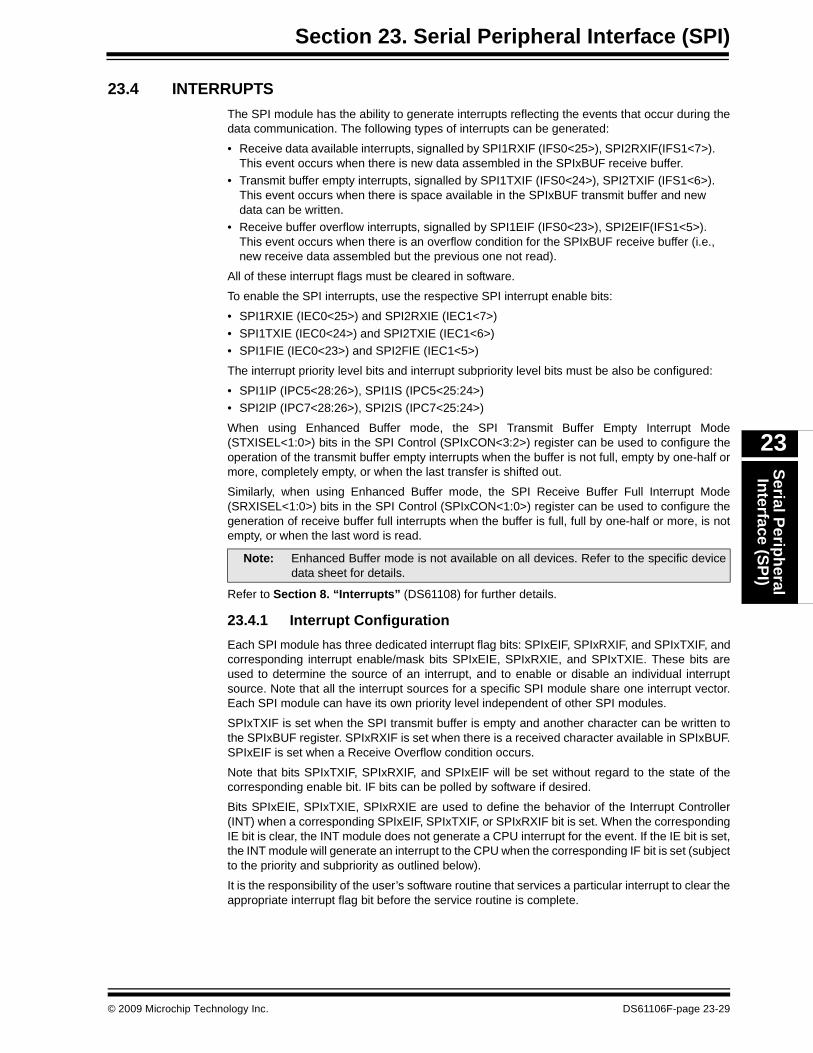
23.4 INTERRUPTSThe SPI module has the ability to generate interrupts reflecting the events that occur during thedata communication. The following types of interrupts can be generated:
• Receive data available interrupts, signalled by SPI1RXIF (IFS0<25>), SPI2RXIF(IFS1<7>). This event occurs when there is new data assembled in the SPIxBUF receive buffer.
• Transmit buffer empty interrupts, signalled by SPI1TXIF (IFS0<24>), SPI2TXIF (IFS1<6>). This event occurs when there is space available in the SPIxBUF transmit buffer and new data can be written.
• Receive buffer overflow interrupts, signalled by SPI1EIF (IFS0<23>), SPI2EIF(IFS1<5>). This event occurs when there is an overflow condition for the SPIxBUF receive buffer (i.e., new receive data assembled but the previous one not read).
All of these interrupt flags must be cleared in software.
To enable the SPI interrupts, use the respective SPI interrupt enable bits:
• SPI1RXIE (IEC0<25>) and SPI2RXIE (IEC1<7>)• SPI1TXIE (IEC0<24>) and SPI2TXIE (IEC1<6>)• SPI1FIE (IEC0<23>) and SPI2FIE (IEC1<5>)
The interrupt priority level bits and interrupt subpriority level bits must be also be configured:
• SPI1IP (IPC5<28:26>), SPI1IS (IPC5<25:24>)• SPI2IP (IPC7<28:26>), SPI2IS (IPC7<25:24>)
When using Enhanced Buffer mode, the SPI Transmit Buffer Empty Interrupt Mode(STXISEL<1:0>) bits in the SPI Control (SPIxCON<3:2>) register can be used to configure theoperation of the transmit buffer empty interrupts when the buffer is not full, empty by one-half ormore, completely empty, or when the last transfer is shifted out.
Similarly, when using Enhanced Buffer mode, the SPI Receive Buffer Full Interrupt Mode(SRXISEL<1:0>) bits in the SPI Control (SPIxCON<1:0>) register can be used to configure thegeneration of receive buffer full interrupts when the buffer is full, full by one-half or more, is notempty, or when the last word is read.
Refer to Section 8. “Interrupts” (DS61108) for further details.
23.4.1 Interrupt ConfigurationEach SPI module has three dedicated interrupt flag bits: SPIxEIF, SPIxRXIF, and SPIxTXIF, andcorresponding interrupt enable/mask bits SPIxEIE, SPIxRXIE, and SPIxTXIE. These bits areused to determine the source of an interrupt, and to enable or disable an individual interruptsource. Note that all the interrupt sources for a specific SPI module share one interrupt vector.Each SPI module can have its own priority level independent of other SPI modules.
SPIxTXIF is set when the SPI transmit buffer is empty and another character can be written tothe SPIxBUF register. SPIxRXIF is set when there is a received character available in SPIxBUF.SPIxEIF is set when a Receive Overflow condition occurs.
Note that bits SPIxTXIF, SPIxRXIF, and SPIxEIF will be set without regard to the state of thecorresponding enable bit. IF bits can be polled by software if desired.
Bits SPIxEIE, SPIxTXIE, SPIxRXIE are used to define the behavior of the Interrupt Controller(INT) when a corresponding SPIxEIF, SPIxTXIF, or SPIxRXIF bit is set. When the correspondingIE bit is clear, the INT module does not generate a CPU interrupt for the event. If the IE bit is set,the INT module will generate an interrupt to the CPU when the corresponding IF bit is set (subjectto the priority and subpriority as outlined below).
It is the responsibility of the user’s software routine that services a particular interrupt to clear theappropriate interrupt flag bit before the service routine is complete.
Note: Enhanced Buffer mode is not available on all devices. Refer to the specific devicedata sheet for details.
© 2009 Microchip Technology Inc. DS61106F-page 23-29

PIC32MX Family Reference Manual
The priority of each SPI module can be set independently with the SPIxIP<2:0> bits. This prioritydefines the priority group to which the interrupt source will be assigned. The priority groups rangefrom a value of 7 (the highest priority), to a value of 0 (which does not generate an interrupt). Aninterrupt being serviced will be preempted by an interrupt in a higher priority group.
The subpriority bits allow setting the priority of an interrupt source within a priority group. Thevalues of the subpriority SPIxIS<1:0> range from 3 (the highest priority) to 0, the lowest priority.An interrupt within the same priority group but having a higher subpriority value will not preempta lower subpriority interrupt that is in progress.
The priority group and subpriority bits allow more than one interrupt source to share the samepriority and subpriority. If simultaneous interrupts occur in this configuration the natural order ofthe interrupt sources within a Priority/subpriority group pair determine the interrupt generated.The natural priority is based on the vector numbers of the interrupt sources. The lower the vectornumber the higher the natural priority of the interrupt. Any interrupts that were overridden bynatural order will then generate their respective interrupts based on Priority, subpriority, andnatural order, after the interrupt flag for the current interrupt is cleared.
After an enabled interrupt is generated, the CPU will jump to the vector assigned to that interrupt.The vector number for the interrupt is the same as the natural order number. The CPU will thenbegin executing code at the vector address. The user’s code at this vector address shouldperform any application-specific operations required, and clear interrupt flags SPIxEIF,SPIxTXIF, or SPIxRXIF, and then exit. Refer to the vector address table details in the Section 8.“Interrupts” (DS61108) for more information on interrupts.
Example 23-3: SPI Initialization with Interrupts Enabled Code Example
Example 23-4: SPI1 ISR Code Example
/*The following code example illustrates an SPI1 interrupt configuration.When the SPI1 interrupt is generated, the cpu will jump to the vector assigned to SPI1interrupt.It assumes that none of the SPI1 input pins are shared with an analog input. If so, the AD1PCFG and corresponding TRIS registers have to be properly configured.
*/
int rData;
IEC0CLR=0x03800000; // disable all SPI interruptsSPI1CON = 0; // Stops and resets the SPI1. rData=SPI1BUF; // clears the receive bufferIFS0CLR=0x03800000; // clear any existing eventIPC5CLR=0x1f000000; // clear the priorityIPC5SET=0x0d000000; // Set IPL=3, Subpriority 1IEC0SET=0x03800000; // Enable RX, TX and Error interrupts
SPI1BRG=0x1; // use FPB/4 clock frequencySPI1STATCLR=0x40; // clear the OverflowSPI1CON=0x8220; // SPI ON, 8 bits transfer, SMP=1, Master mode
/*The following code example demonstrates a simple interrupt service routine for SPI1interrupts. The user’s code at this vector should perform any application specific operationsand must clear the SPI1 interrupt flags before exiting.
*/
void __ISR(_SPI_1_VECTOR, ipl3)__SPI1Interrupt(void){
// ... perform application specific operations in response to the// interrupt
IFS0CLR = 0x03800000; // Be sure to clear the SPI1 interrupt flags// before exiting the service routine.
}
DS61106F-page 23-30 © 2009 Microchip Technology Inc.

Section 23. Serial Peripheral Interface (SPI)Serial Peripheral
Interface (SPI)
23
For devices with Enhanced Buffering mode, the user application should clear the interruptrequest flag after servicing the interrupt condition.
If an SPI interrupt has occurred, the ISR should read the SPI Data Buffer (SPIxBUF) register, andthen clear the SPI interrupt flag, as shown in Example 23-5.
Example 23-5: SPI1 ISR Code Example for Devices With Enhanced Buffering Mode/*
The following code example demonstrates a simple interrupt service routine for SPI1interrupts. The user’s code at this vector should perform any application specific operationsand must clear the SPI1 interrupt flags before exiting.
*/
void __ISR(_SPI_1_VECTOR, ipl3)__SPI1Interrupt(void){
int Data; // Read SPI data bufferData = SPI1BUF;
// ... perform application specific operations in response to the// interrupt
IFS0CLR = 0x03800000; // Be sure to clear the SPI1 interrupt flags// before exiting the service routine.
}
Note: The SPI1 ISR code examples show MPLAB® C32 C compiler specific syntax. Refer to your compilermanual regarding support for ISRs.
© 2009 Microchip Technology Inc. DS61106F-page 23-31

PIC32MX Family Reference Manual
23.5 OPERATION IN POWER-SAVING AND DEBUG MODES
23.5.1 Sleep ModeWhen the device enters Sleep mode, the system clock is disabled. The exact SPI moduleoperation during Sleep mode depends on the current mode of operation. The followingsubsections describe mode-specific behavior.
23.5.1.1 MASTER MODE IN SLEEP MODE
The following items should be noted in Sleep mode:
• The Baud Rate Generator is stopped and reset.• On-going transmission and reception sequences are aborted. The module will not resume
aborted sequences when Sleep mode is exited.• Once in Sleep mode, the module will not transmit or receive any new data.
23.5.1.2 SLAVE MODE IN SLEEP MODE
In the Slave mode, the SPI module operates from the SCK provided by an external SPI Master.Since the clock pulses at SCKx are externally provided for Slave mode, the module will continueto function in Sleep mode. It will complete any transactions during the transition into Sleep. Oncompletion of a transaction, the SPIRBF flag is set. Consequently, bit SPIxRXIF will be set. If SPIinterrupts are enabled (SPIxRXIE = 1) and the SPI interrupt priority level is greater than thepresent CPU priority level, the device will wake from Sleep mode and the code execution willresume at the SPIx interrupt vector location. If the SPI interrupt priority level is lower than or equalto the present CPU priority level, the CPU will remain in Idle mode.
The module is not reset on entering Sleep mode if it is operating as a slave device. Registercontents are not affected when the SPIx module is going into or coming out of Sleep mode.
23.5.2 Idle ModeWhen the device enters Idle mode, the system clock sources remain functional.
23.5.2.1 MASTER MODE IN IDLE MODE
Bit SIDL (SPIxCON<13>) selects whether the module will stop or continue functioning in Idlemode.
• If SIDL = 1, the module will discontinue operation in Idle mode. The module will perform the same procedures when stopped in Idle mode that it does for Sleep mode.
• If SIDL = 0, the module will continue operation in Idle mode.
23.5.2.2 SLAVE MODE IN IDLE MODE
The module will continue operation in Idle mode irrespective of the SIDL setting. The behavior isidentical to the one in Sleep mode.
23.5.3 Debug ModeBit FRZ (SPIxCON<14>) determines whether the SPI module will run or stop while the CPU isexecuting Debug exception code (i.e., application is halted) in Debug mode. When FRZ = 0, theSPI module continues to run, even when the application is halted in Debug mode. When FRZ = 1and the application is halted in Debug mode, the behavior is different from Master-to-Slavemode.
23.5.3.1 FREEZE IN MASTER MODE
When FRZ = 1 and the application is halted in Debug mode, the module will freeze its operationsand make no changes to the state of the SPI module, such that it will continue exactly as it leftoff. In other words, the transmission/reception is not aborted during this halt.
Note: To prevent unintentional abort of transmit and receive sequences, wait for thecurrent transmission to be completed before activating Sleep mode.
DS61106F-page 23-32 © 2009 Microchip Technology Inc.

Section 23. Serial Peripheral Interface (SPI)Serial Peripheral
Interface (SPI)
23
23.5.3.2 FREEZE IN SLAVE MODE
In Slave mode with an externally provided SCK, the module will continue to operate, even thoughit is frozen (FRZ = 1), i.e., the shift register is functional. However, when data is received in theshift register before Debug mode is exited, the data that has been received is ignored (i.e., nottransferred to SPIxBUF).
23.5.3.3 OPERATION OF SPIXBUF
23.5.3.3.1 Reads During Debug ModeDuring Debug mode, SPIxBUF can be read; but the read operation does not affect any Statusbits. For example, if bit SPIRBF (SPIxSTAT<0>) is set when Debug mode is entered, it will remainset on EXIT From Debug mode, even though the SPIxBUF register was read in Debug mode.
23.5.3.3.2 Writes During Debug ModeWhen FRZ is set, write functionality depends on whether the SPI is in Master or Slave mode.
In Master mode: the write operation will place the data in the buffer, but the transmission will notstart until the Debug mode is exited.
In Slave mode: the write operation will place the data in the buffer, and the data will be sent outwhenever the Master initiates a new transaction, even if the device is still in Debug mode.
Note: The FRZ bit is readable and writable only when the CPU is executing in DebugException mode. In all other modes, the FRZ bit reads as ‘0’. If FRZ bit is changedduring Debug mode, the new value does not take effect until the current DebugException mode is exited and re-entered. During the Debug Exception mode, theFRZ bit reads the state of the peripheral when entering Debug mode.
© 2009 Microchip Technology Inc. DS61106F-page 23-33

PIC32MX Family Reference Manual
23.6 EFFECTS OF VARIOUS RESETS
23.6.1 Device ResetAll SPI registers are forced to their Reset states upon a device Reset. When the asynchronousReset input goes active, the SPI logic:
• Resets all fields in SPIxCON and SPIxSTAT• Resets the transmit and receive buffers (SPIx-BUF) to the empty state• Resets the Baud Rate Generator
23.6.2 Power-on ResetAll SPI registers are forced to their Reset states when a Power-on Reset occurs.
23.6.3 Watchdog Timer ResetAll SPI registers are forced to their Reset states when a Watchdog Timer Reset occurs.
23.7 PERIPHERALS USING SPI MODULESThere are no other peripherals using the SPI module.
DS61106F-page 23-34 © 2009 Microchip Technology Inc.

Section 23. Serial Peripheral Interface (SPI)Serial Peripheral
Interface (SPI)
23
23.8 DESIGN TIPS
Question 1: Can I use the SSx pin as an output to a slave device when the PIC32MXfamily SPI module is configured in Master mode?
Answer: Yes, you can. Notice, however, that the SSx pin is not driven by the SPI Master.You have to drive the bit yourself and pulse it before the SPI transmission takesplace. You can use any other I/O pin for that purpose.
Question 1: If I do not use the SDO output for my SPI module, is this I/O pin available asa general purpose I/O pin?
Answer: Yes. If you are not interested in transmitting data, only receiving, you can use theSDO pin as a general I/O pin. This is mainly useful for SPI modules that areconfigured as SPI slave devices. Note that when used as a general purpose I/Opin, the user is responsible for configuring the respective data direction register(TRIS) for input or output.
© 2009 Microchip Technology Inc. DS61106F-page 23-35

PIC32MX Family Reference Manual
23.9 RELATED APPLICATION NOTESThis section lists application notes that are related to this section of the manual. Theseapplication notes may not be written specifically for the PIC32MX family device family, but theconcepts are pertinent and could be used with modification and possible limitations. The currentapplication notes related to the SPI module are:
Title Application Note #Interfacing Microchip’s MCP41XXX/MCP42XXX Digital Potentiometers to a PIC® Microcontroller
AN746
Interfacing Microchip’s MCP3201 Analog-to-Digital Converter to the PIC® Microcontroller AN719
Note: Please visit the Microchip web site (www.microchip.com) for additional applicationnotes and code examples for the PIC32MX family of devices.
DS61106F-page 23-36 © 2009 Microchip Technology Inc.
Section 23. Serial Peripheral Interface (SPI)Serial Peripheral
Interface (SPI)
23
23.10 REVISION HISTORY
Revision A (July 2007)This is the initial released version of this document.
Revision B (October 2007)Revised Examples 23-1, 23-2, 23-3; Table 23-5.
Revision C (October 2007)Updated document to remove Confidential status.
Revision D (April 2008)Revised status to Preliminary; Revised U-0 to r-x.
Revision E (June 2008)Added Footnote number to Registers 12-12-17; Revised Example 23-4; Revised Figure 23-8;Change Reserved bits from “Maintain as” to “Write”; Added Note to ON bit (SPIxCON Register).
Revision F (August 2009)This revision includes the following changes:
• Minor changes to the text and formatting have been incorporated through the document• Updated register introductions in Section 23.2 “Status and Control Registers”• Register Summary (Table 23-2)
- Removed references to the Clear, Set, Invert, IFS0, IFS1, IEC0, IEC1, IPC5, and IPC7 registers
- Added the Address Offset column- Added Notes 1, 2, and 3, which describe the Clear, Set, and Invert registers- Added these bits: MSSEN, FRMSYPW, FRMCNT<2:0>, ENHBUF, STXISEL<1:0>,
SRXISEL<1:0>, RXBUFELM<4:0>, SPITUR, SRMT, SPIRBE, AND SPITBF• Removed the IFS0, IFS1, IEC0, IEC1, IPC5, and IPC7 registers• Added Notes describing the Clear, Set, and Invert registers to the following registers:
- SPIxCON- SPIxSTAT- SPIxBRG
• Added SPIxBRG settings for 60, 72, and 80 MHz in the Sample SCKx Frequencies table (see Table 23-3)
• Removed SPI Interrupt Vectors for Various Offsets table (Table 23-4)• Added Section 23.3.2 “Buffer Modes”• Added a paragraph that provides details on the MSSEN bit in Section 23.3.3.1 “Master
Mode Operation”• Added two bullets that provide details on the FRMSYPW and FRMCNT bits in Section
23.3.6 “Framed SPI Modes”• Added two paragraphs that provide details on the STXISEL<1:0> and SRXISEL<1:0> bits
in Section 23.4 “Interrupts”• Added a paragraph on SPI1 ISR for devices with Enhanced Buffering mode after
Example 23-4 in 23.4.1 “Interrupt Configuration”• Added SPI1 ISR Code Example for Devices With Enhanced Buffering mode (see
Example 23-5).• Removed Section 23.8 “I/O Pin Control”
© 2009 Microchip Technology Inc. DS61106F-page 23-37

PIC32MX Family Reference Manual
NOTES:
DS61106F-page 23-38 © 2009 Microchip Technology Inc.