selected topics in photonics/optoelectronics research … · selected topics in...
TRANSCRIPT
Selected Topics in Photonics/Optoelectronics Researchat the University of Cincinnati
The purpose of this article is to provide an overview of the research activities in photonics and optoelectronics being carried out at the Univer-sity of Cincinnati (UC). The article presents brief summaries of several topics covering research in optical sensors, near-field optical microscopy,optical displays, optical memory, visible and infrared light emitters. The summaries are certainly not comprehensive, nor does this article capturethe totality of photonics-related research at UC. It is only intended to provide a window on our activities through which we encourage the readersto learn more by contacting us. Faculty with interest in photonics and optoelectronics at UC span a variety of disciplines including Electrical En-gineering, Materials Science, Physics, Medicine, etc.
Compiled by Prof. A. J. StecklUniversity of Cincinnati
Cincinnati, OH 45221([email protected])
Optically Interrogated MEMS Pressure Sensors for PropulsionApplicationsProf J. T. Boyd and Prof H. E. [email protected], [email protected]
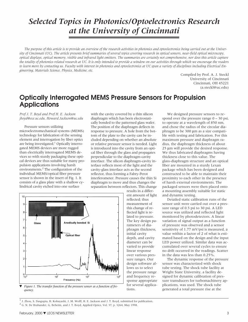
Pressure sensors utilizingmicroelectromechanical systems (MEMS)technology for fabrication of the sensingelement and interrogation by fiber opticsare being investigated.1 Optically interro-gated MEMS devices are more ruggedthan electrically interrogated MEMS de-vices so with sturdy packaging these opti-cal devices are thus suitable for many pro-pulsion applications involving harshenvironments.2 The configuration of theindividual MEMS/optical fiber pressuresensor is shown in the insert of Fig. 1. Itconsists of a glass plate with a shallow cy-lindrical cavity etched into one surface
with the cavity covered by a thin silicondiaphragm which has been electrostati-cally bonded to the patterned glass wafer.The position of the diaphragm deflects inresponse to pressure. A hole from the bot-tom of the plate to the cavity can be in-cluded depending on whether an absoluteor relative pressure sensor is needed. Lightis introduced into the cavity from an opti-cal fiber through the glass and propagatesperpendicular to the diaphragm-cavityinterface. The silicon diaphragm-cavity in-terface reflects most of the light and thecavity-glass interface acts as the secondreflector, thus forming a Fabry-Perotinterferometer. Pressure causes the thin Sidiaphragm to move and thus changes theseparation between reflectors. This change
results in a differ-ent amount of lightreflected; thusmeasurement ofthis change of re-flected light is re-lated to pressure.The key design pa-rameters of dia-phragm thickness,initial cavitydepth, and cavitydiameter can bevaried to providelinear responseover various pres-sure ranges. Ourdesign software al-lows us to selectthe pressure rangeand frequency re-sponse appropriatefor several applica-tions.
We designed pressure sensors to re-spond over the pressure range 0 – 30 psi,to operate at a wavelength of 850 nm,and chose the radius of the circular dia-phragm to be 300 µm as a size compati-ble with testing and fabrication. For thismaximum pressure and diaphragm ra-dius, the diaphragm thickness of about25 µm will provide the desired response.We thus fabricated diaphragms havingthickness close to this value. Theglass-diaphragm structure and an opticalfiber are mounted in a sturdy Lexanpackage which has been designed andconstructed to be able to maintain theirproximity to each other in the presenceof harsh external environments. Thepackaged sensors were then placed ontoa mounting assembly suitable for staticand dynamic testing.
Detailed static calibration runs of thesensor unit were carried out over a pres-sure range of 0.5 psi to 30 psi. A LEDsource was utilized and reflected lightmonitored by photodetectors. A linearvariation of signal output as a functionof pressure was observed and a sensorsensitivity of 1.77 mV/psi is measured, avalue within a factor of 2 of what is esti-mated based on the design and the inputLED power utilized. Similar data was ac-cumulated over several cycles to ensureno drift occurred in the readings. Scatterin the data was less than 0.25%.
The dynamic response of the pressuresensor was characterized with shocktube testing. The shock tube facility atWright State University, a facility de-signed for dynamic calibration of pres-sure transducers for turbomachinery ap-plications, was used. The shock tubegenerated a total pressure rise at the
February, 2000 � LEOS NEWSLETTER 3
1 J. Zhou, S. Dasgupta, H. Kobayashi, J. M. Wolff, H. E. Jackson and J. T. Boyd, submitted for publication.2 G. N. De Brabander, G. Beheim, and J. T. Boyd, Applied Optics, Vol. 37, p. 3264, May 1998.
� Figure 1. The transfer function of the pressure sensor as a function of fre-quency.
sensor of about 10 psi. Typical timetraces of the response of the detectordue to the shock wave sampled at a 5MHz rate show sharp response to theshock wave pressure rise. The sensorshows some overshoot before reaching aconstant output. The pressure step mag-nitude is about 10 psi as expected fromthe theoretical calculation.
A frequency response analysis is per-formed by taking 4096 points of data
with a frequency resolution increment1.22 kHz. Multiple time traces were in-dividually analyzed, and then averagedin the frequency domain. The transferfunction as a function of frequency isshown in the attached figure. An impor-tant result of these dynamic calibrationtests is the usable frequency of the fabri-cated sensor. The flat response of thesensor extends up to 30 kHz. Therefore,it has an adequate unsteady pressure
measurement capability for high speedpropulsion applications, such as for gasturbines. Others participating in this re-search include Adjunct Research Assis-tant Professor S. Dasgupta, J. M. Wolf,Assistant Professor at Wright State Uni-versity and graduate student J. Zhou.This work has been supported in part bya joint AFRL/DAGSI (Dayton Area Grad-uate Studies Institute) grant, AFOSR,and NASA.
Near Field Imaging of Vertical Cavity Surface Emitting LasersProf H. E. Jackson and Prof J. T. Boyd
Understanding integrated optic struc-tures, including vertical cavity surfaceemitting laser (VCSEL) structures, requiresa spatial resolution which exceeds the dif-fraction limit. Utilizing near field scanningoptical microscopy (NSOM) and spectros-copy, we have studied in detail the spatialelectric field intensities associated with op-tical channel waveguides3 , directionalcouplers, y-junctions, and, most recently,vertical cavity surface emitting lasers4.VCSELs offer numerous promising appli-cations that take advantage of such excel-lent VCSEL properties as low threshold,integrability into two dimensional laser ar-rays, and high coupling efficiency of theirlight into single mode fibers. We haveused spectrally resolved near field imagingto study small aperture proton implantedVCSELs. The spectroscopy is accomplishedby coupling the light collected by the ~100nm near field tip which is scanned about10 nm above the surface of the sampleinto a spectrometer.
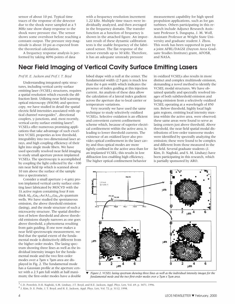
Consider a small aperture (~6 µm) pro-ton implanted vertical cavity surface emit-ting laser fabricated by MOCVD with the1λ active region containing four 8 nmthick Al0.3Ga0.7As/A10.6Ga0.4As quantumwells. We have studied the spontaneousemission, the above threshold emission(lasing), and the mode structure of such amicrocavity structure. The spatial distribu-tion of below threshold and above thresh-old emissions sharply narrows as one goesabove threshold, a phenomena resultingfrom gain guiding. If one now makes anear field spectroscopic measurement, wefind that the spatial extent of the funda-mental mode is distinctively different fromthe higher order modes. The lasing spec-trum showing three lines as well as the in-dividual intensity images for the funda-mental mode and the two first-ordermodes over a 7µm x 7µm area are dis-played in Fig. 2. The fundamental modehas a Gaussian profile at the aperture cen-ter with a 2.5 µm full width at half maxi-mum; the first-order modes have a double
lobed shape with a null at the center. Thefundamental width (2.5 µm) is much lessthan the 6 µm width which indicates thepresence of index guiding at this injectioncurrent. An analysis of these data allowthe calculation of a lateral index gradientacross the aperture due to local carrier ortemperature variations.
Very recently we have used the sametechnique to study selectively oxidizedVCSELs. Selective oxidation is an efficientand convenient current confinementscheme which, because of superior electri-cal confinement within the active area, isleading to lower threshold currents. Theexistence of an oxidized layer also pro-vides optical confinement in the laser cav-ity and thus optical modes are moretightly confined in the active area than foran implanted VCSEL; this results in lowdiffraction loss enabling high efficiency.The higher optical confinement behavior
in oxidized VCSELs also results in moredistinct and complex multimode emission,demanding a novel method to identify theVCSEL modal structures. We have ob-tained spatially and spectrally resolved im-ages of both subthreshold emission andlasing emission from a selectively oxidizedVCSEL operating at a wavelength of 850nm. Below threshold, highly local highgain regions, emitting local intensity max-ima within the active area, were observed;these same areas were found to serve aslasing centers just above threshold. Abovethreshold, the near field spatial modal dis-tributions of low-order transverse modeswere identified by spectrally analyzing theemission; these were found to be complexand different from those measured in thefar field. Several graduate students (J.Kim, D. Naghski, and S. M. Lindsay) havebeen participating in this research, whichis partially sponsored by ARO.
4 LEOS NEWSLETTER � February, 2000
3 C.D. Poweleit, D.H. Naghski, S.M. Lindsay, J.T. Boyd, and H.E. Jackson, Appl. Phys. Lett, Vol. 69, p. 3471, 1996.4 J. Kim, D. E. Pride, J. T. Boyd, and H. E. Jackson, Appl. Phys. Lett, Vol. 72, p. 3112, 1998.
� Figure 2. VCSEL lasing spectrum showing three lines as well as the individual intensity images for thefundamental mode and the two first-order modes over a 7µm x 7µm area.
3-D IC Vision Display using MEMS TechnologyProf S. T. Kowel ([email protected] )
The goal of IC Vision is to produce areal-time, full-color, autostereoscopic dis-play. Depth perception and motion paral-lax are provided by integrating flat-paneldisplays with directing optics. A directingarray directs modulated light to a set ofvirtual viewing zones in space, displayinga series of stereoscopic image pairs whichcan be easily fused by the viewer. Noheadgear is required to view these imagesgenerated with incoherent light. Two ap-proaches have been investigated -diffractive gratings and reflective MEMSmicromirrors. Prototype displays werebased on the diffractive partial pixels ap-proach, in which gratings direct differentviews into appropriate viewing zones.5
However, the major challenge is how tomake a larger screen display while main-taining color and high resolution. Sincethe partial pixels were spatially multi-plexed for eight stereo pairs (16 views)and three prime colors, a large number ofpixels is required to maintain resolution.As an example, a color VGA (640×480)display with 16 views will need640×480×16×3 ≈ 14.7 million partial pix-els, far beyond current capabilities.
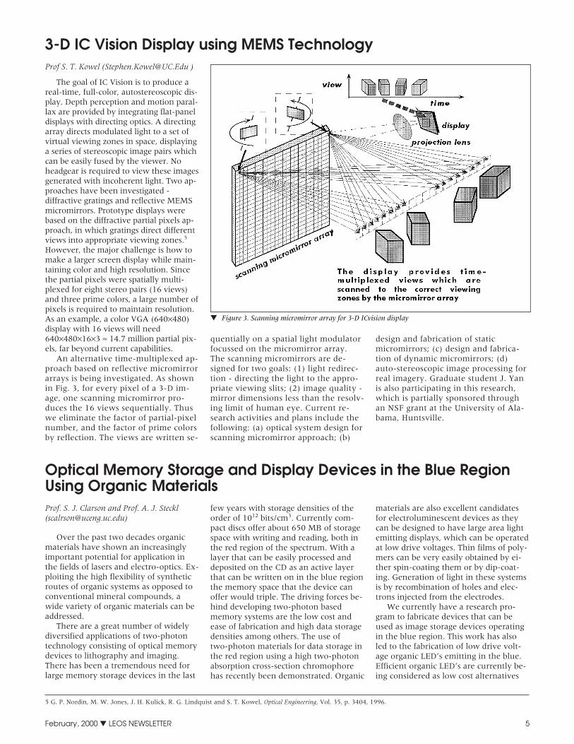
An alternative time-multiplexed ap-proach based on reflective micromirrorarrays is being investigated. As shownin Fig. 3, for every pixel of a 3-D im-age, one scanning micromirror pro-duces the 16 views sequentially. Thuswe eliminate the factor of partial-pixelnumber, and the factor of prime colorsby reflection. The views are written se-
quentially on a spatial light modulatorfocussed on the micromirror array.The scanning micromirrors are de-signed for two goals: (1) light redirec-tion - directing the light to the appro-priate viewing slits; (2) image quality -mirror dimensions less than the resolv-ing limit of human eye. Current re-search activities and plans include thefollowing: (a) optical system design forscanning micromirror approach; (b)
design and fabrication of staticmicromirrors; (c) design and fabrica-tion of dynamic micromirrors; (d)auto-stereoscopic image processing forreal imagery. Graduate student J. Yanis also participating in this research,which is partially sponsored throughan NSF grant at the University of Ala-bama, Huntsville.
Optical Memory Storage and Display Devices in the Blue RegionUsing Organic MaterialsProf. S. J. Clarson and Prof. A. J. Steckl([email protected])
Over the past two decades organicmaterials have shown an increasinglyimportant potential for application inthe fields of lasers and electro-optics. Ex-ploiting the high flexibility of syntheticroutes of organic systems as opposed toconventional mineral compounds, awide variety of organic materials can beaddressed.
There are a great number of widelydiversified applications of two-photontechnology consisting of optical memorydevices to lithography and imaging.There has been a tremendous need forlarge memory storage devices in the last
few years with storage densities of theorder of 1012 bits/cm3. Currently com-pact discs offer about 650 MB of storagespace with writing and reading, both inthe red region of the spectrum. With alayer that can be easily processed anddeposited on the CD as an active layerthat can be written on in the blue regionthe memory space that the device canoffer would triple. The driving forces be-hind developing two-photon basedmemory systems are the low cost andease of fabrication and high data storagedensities among others. The use oftwo-photon materials for data storage inthe red region using a high two-photonabsorption cross-section chromophorehas recently been demonstrated. Organic
materials are also excellent candidatesfor electroluminescent devices as theycan be designed to have large area lightemitting displays, which can be operatedat low drive voltages. Thin films of poly-mers can be very easily obtained by ei-ther spin-coating them or by dip-coat-ing. Generation of light in these systemsis by recombination of holes and elec-trons injected from the electrodes.
We currently have a research pro-gram to fabricate devices that can beused as image storage devices operatingin the blue region. This work has alsoled to the fabrication of low drive volt-age organic LED’s emitting in the blue.Efficient organic LED’s are currently be-ing considered as low cost alternatives
February, 2000 � LEOS NEWSLETTER 5
5 G. P. Nordin, M. W. Jones, J. H. Kulick, R. G. Lindquist and S. T. Kowel, Optical Engineering, Vol. 35, p. 3404, 1996.
� Figure 3. Scanning micromirror array for 3-D ICvision display
for applications such as backlights in liq-uid-crystal displays, automotive domelights and other illumination purposes.
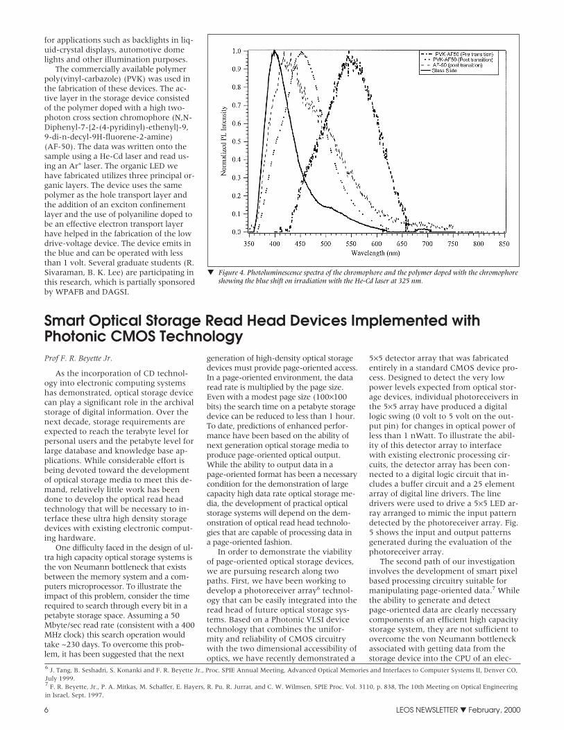
The commercially available polymerpoly(vinyl-carbazole) (PVK) was used inthe fabrication of these devices. The ac-tive layer in the storage device consistedof the polymer doped with a high two-photon cross section chromophore (N,N-Diphenyl-7-{2-(4-pyridinyl)-ethenyl}-9,9-di-n-decyl-9H-fluorene-2-amine)(AF-50). The data was written onto thesample using a He-Cd laser and read us-ing an Ar+ laser. The organic LED wehave fabricated utilizes three principal or-ganic layers. The device uses the samepolymer as the hole transport layer andthe addition of an exciton confinementlayer and the use of polyaniline doped tobe an effective electron transport layerhave helped in the fabrication of the lowdrive-voltage device. The device emits inthe blue and can be operated with lessthan 1 volt. Several graduate students (R.Sivaraman, B. K. Lee) are participating inthis research, which is partially sponsoredby WPAFB and DAGSI.
Smart Optical Storage Read Head Devices Implemented withPhotonic CMOS TechnologyProf F. R. Beyette Jr.
As the incorporation of CD technol-ogy into electronic computing systemshas demonstrated, optical storage devicecan play a significant role in the archivalstorage of digital information. Over thenext decade, storage requirements areexpected to reach the terabyte level forpersonal users and the petabyte level forlarge database and knowledge base ap-plications. While considerable effort isbeing devoted toward the developmentof optical storage media to meet this de-mand, relatively little work has beendone to develop the optical read headtechnology that will be necessary to in-terface these ultra high density storagedevices with existing electronic comput-ing hardware.
One difficulty faced in the design of ul-tra high capacity optical storage systems isthe von Neumann bottleneck that existsbetween the memory system and a com-puters microprocessor. To illustrate theimpact of this problem, consider the timerequired to search through every bit in apetabyte storage space. Assuming a 50Mbyte/sec read rate (consistent with a 400MHz clock) this search operation wouldtake ~230 days. To overcome this prob-lem, it has been suggested that the next
generation of high-density optical storagedevices must provide page-oriented access.In a page-oriented environment, the dataread rate is multiplied by the page size.Even with a modest page size (100×100bits) the search time on a petabyte storagedevice can be reduced to less than 1 hour.To date, predictions of enhanced perfor-mance have been based on the ability ofnext generation optical storage media toproduce page-oriented optical output.While the ability to output data in apage-oriented format has been a necessarycondition for the demonstration of largecapacity high data rate optical storage me-dia, the development of practical opticalstorage systems will depend on the dem-onstration of optical read head technolo-gies that are capable of processing data ina page-oriented fashion.
In order to demonstrate the viabilityof page-oriented optical storage devices,we are pursuing research along twopaths. First, we have been working todevelop a photoreceiver array6 technol-ogy that can be easily integrated into theread head of future optical storage sys-tems. Based on a Photonic VLSI devicetechnology that combines the unifor-mity and reliability of CMOS circuitrywith the two dimensional accessibility ofoptics, we have recently demonstrated a
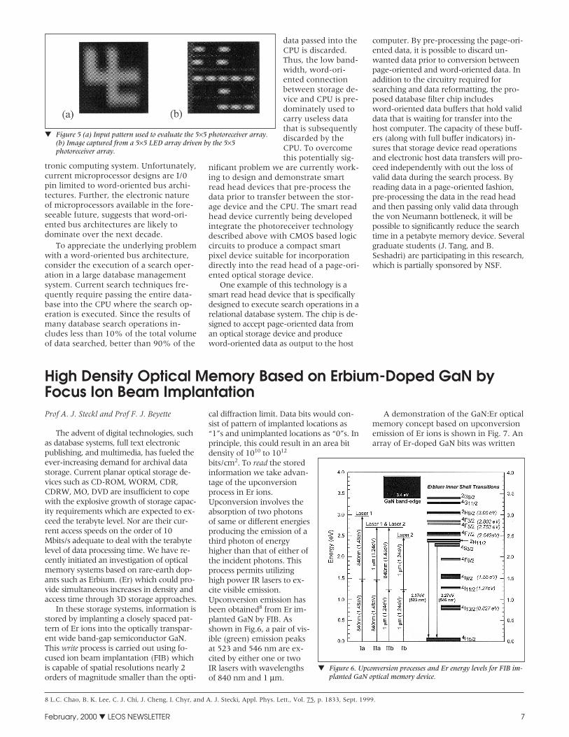
5×5 detector array that was fabricatedentirely in a standard CMOS device pro-cess. Designed to detect the very lowpower levels expected from optical stor-age devices, individual photoreceivers inthe 5×5 array have produced a digitallogic swing (0 volt to 5 volt on the out-put pin) for changes in optical power ofless than 1 nWatt. To illustrate the abil-ity of this detector array to interfacewith existing electronic processing cir-cuits, the detector array has been con-nected to a digital logic circuit that in-cludes a buffer circuit and a 25 elementarray of digital line drivers. The linedrivers were used to drive a 5×5 LED ar-ray arranged to mimic the input patterndetected by the photoreceiver array. Fig.5 shows the input and output patternsgenerated during the evaluation of thephotoreceiver array.
The second path of our investigationinvolves the development of smart pixelbased processing circuitry suitable formanipulating page-oriented data.7 Whilethe ability to generate and detectpage-oriented data are clearly necessarycomponents of an efficient high capacitystorage system, they are not sufficient toovercome the von Neumann bottleneckassociated with getting data from thestorage device into the CPU of an elec-
6 LEOS NEWSLETTER � February, 2000
� Figure 4. Photoluminescence spectra of the chromophore and the polymer doped with the chromophoreshowing the blue shift on irradiation with the He-Cd laser at 325 nm.
6 J. Tang, B. Seshadri, S. Konanki and F. R. Beyette Jr., Proc. SPIE Annual Meeting, Advanced Optical Memories and Interfaces to Computer Systems II, Denver CO,July 1999.7 F. R. Beyette, Jr., P. A. Mitkas, M. Schaffer, E. Hayers, R. Pu. R. Jurrat, and C. W. Wilmsen, SPIE Proc. Vol. 3110, p. 838, The 10th Meeting on Optical Engineeringin Israel, Sept. 1997.
tronic computing system. Unfortunately,current microprocessor designs are I/0pin limited to word-oriented bus archi-tectures. Further, the electronic natureof microprocessors available in the fore-seeable future, suggests that word-ori-ented bus architectures are likely todominate over the next decade.
To appreciate the underlying problemwith a word-oriented bus architecture,consider the execution of a search oper-ation in a large database managementsystem. Current search techniques fre-quently require passing the entire data-base into the CPU where the search op-eration is executed. Since the results ofmany database search operations in-cludes less than 10% of the total volumeof data searched, better than 90% of the
data passed into theCPU is discarded.Thus, the low band-width, word-ori-ented connectionbetween storage de-vice and CPU is pre-dominately used tocarry useless datathat is subsequentlydiscarded by theCPU. To overcomethis potentially sig-
nificant problem we are currently work-ing to design and demonstrate smartread head devices that pre-process thedata prior to transfer between the stor-age device and the CPU. The smart readhead device currently being developedintegrate the photoreceiver technologydescribed above with CMOS based logiccircuits to produce a compact smartpixel device suitable for incorporationdirectly into the read head of a page-ori-ented optical storage device.
One example of this technology is asmart read head device that is specificallydesigned to execute search operations in arelational database system. The chip is de-signed to accept page-oriented data froman optical storage device and produceword-oriented data as output to the host
computer. By pre-processing the page-ori-ented data, it is possible to discard un-wanted data prior to conversion betweenpage-oriented and word-oriented data. Inaddition to the circuitry required forsearching and data reformatting, the pro-posed database filter chip includesword-oriented data buffers that hold validdata that is waiting for transfer into thehost computer. The capacity of these buff-ers (along with full buffer indicators) in-sures that storage device read operationsand electronic host data transfers will pro-ceed independently with out the loss ofvalid data during the search process. Byreading data in a page-oriented fashion,pre-processing the data in the read headand then passing only valid data throughthe von Neumann bottleneck, it will bepossible to significantly reduce the searchtime in a petabyte memory device. Severalgraduate students (J. Tang, and B.Seshadri) are participating in this research,which is partially sponsored by NSF.
High Density Optical Memory Based on Erbium-Doped GaN byFocus Ion Beam ImplantationProf A. J. Steckl and Prof F. J. Beyette
The advent of digital technologies, suchas database systems, full text electronicpublishing, and multimedia, has fueled theever-increasing demand for archival datastorage. Current planar optical storage de-vices such as CD-ROM, WORM, CDR,CDRW, MO, DVD are insufficient to copewith the explosive growth of storage capac-ity requirements which are expected to ex-ceed the terabyte level. Nor are their cur-rent access speeds on the order of 10Mbits/s adequate to deal with the terabytelevel of data processing time. We have re-cently initiated an investigation of opticalmemory systems based on rare-earth dop-ants such as Erbium. (Er) which could pro-vide simultaneous increases in density andaccess time through 3D storage approaches.
In these storage systems, information isstored by implanting a closely spaced pat-tern of Er ions into the optically transpar-ent wide band-gap semiconductor GaN.This write process is carried out using fo-cused ion beam implantation (FIB) whichis capable of spatial resolutions nearly 2orders of magnitude smaller than the opti-
cal diffraction limit. Data bits would con-sist of pattern of implanted locations as“1”s and unimplanted locations as “0”s. Inprinciple, this could result in an area bitdensity of 1010 to 1012
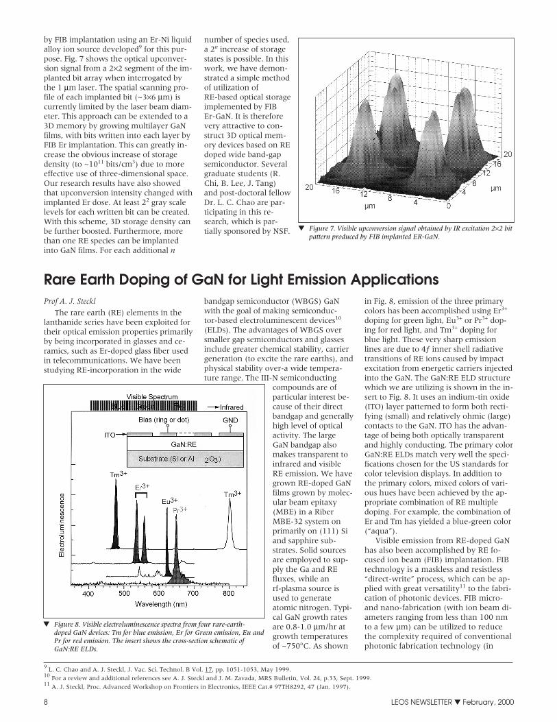
bits/cm2. To read the storedinformation we take advan-tage of the upconversionprocess in Er ions.Upconversion involves theabsorption of two photonsof same or different energiesproducing the emission of athird photon of energyhigher than that of either ofthe incident photons. Thisprocess permits utilizinghigh power IR lasers to ex-cite visible emission.Upconversion emission hasbeen obtained8 from Er im-planted GaN by FIB. Asshown in Fig.6, a pair of vis-ible (green) emission peaksat 523 and 546 nm are ex-cited by either one or twoIR lasers with wavelengthsof 840 nm and 1 µm.
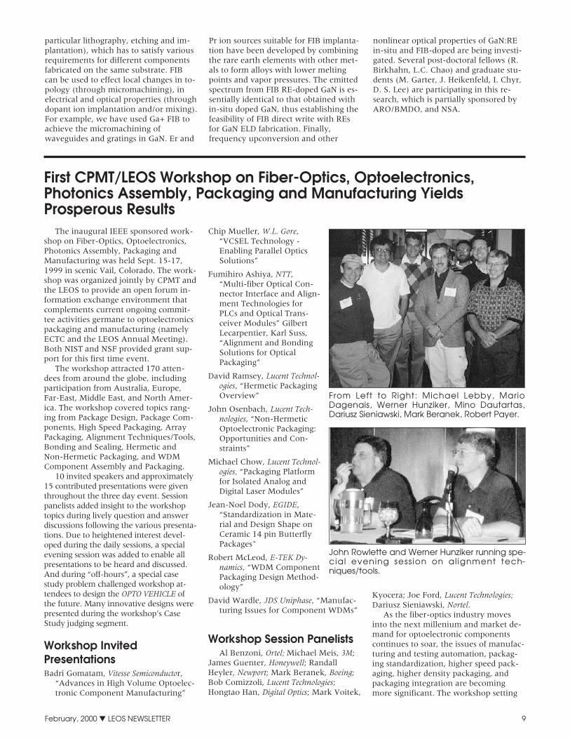
A demonstration of the GaN:Er opticalmemory concept based on upconversionemission of Er ions is shown in Fig. 7. Anarray of Er-doped GaN bits was written
February, 2000 � LEOS NEWSLETTER 7
� Figure 5 (a) Input pattern used to evaluate the 5×5 photoreceiver array.(b) Image captured from a 5×5 LED array driven by the 5×5photoreceiver array.
8 L.C. Chao, B. K. Lee, C. J. Chi, J. Cheng, I. Chyr, and A. J. Stecki, Appl. Phys. Lett., Vol. 75, p. 1833, Sept. 1999.
� Figure 6. Upconversion processes and Er energy levels for FIB im-planted GaN optical memory device.
by FIB implantation using an Er-Ni liquidalloy ion source developed9 for this pur-pose. Fig. 7 shows the optical upconver-sion signal from a 2×2 segment of the im-planted bit array when interrogated bythe 1 µm laser. The spatial scanning pro-file of each implanted bit (~3×6 µm) iscurrently limited by the laser beam diam-eter. This approach can be extended to a3D memory by growing multilayer GaNfilms, with bits written into each layer byFIB Er implantation. This can greatly in-crease the obvious increase of storagedensity (to ~1011 bits/cm3) due to moreeffective use of three-dimensional space.Our research results have also showedthat upconversion intensity changed withimplanted Er dose. At least 22 gray scalelevels for each written bit can be created.With this scheme, 3D storage density canbe further boosted. Furthermore, morethan one RE species can be implantedinto GaN films. For each additional n
number of species used,a 2n increase of storagestates is possible. In thiswork, we have demon-strated a simple methodof utilization ofRE-based optical storageimplemented by FIBEr-GaN. It is thereforevery attractive to con-struct 3D optical mem-ory devices based on REdoped wide band-gapsemiconductor. Severalgraduate students (R.Chi, B. Lee, J. Tang)and post-doctoral fellowDr. L. C. Chao are par-ticipating in this re-search, which is par-tially sponsored by NSF.
Rare Earth Doping of GaN for Light Emission ApplicationsProf A. J. Steckl
The rare earth (RE) elements in thelanthanide series have been exploited fortheir optical emission properties primarilyby being incorporated in glasses and ce-ramics, such as Er-doped glass fiber usedin telecommunications. We have beenstudying RE-incorporation in the wide
bandgap semiconductor (WBGS) GaNwith the goal of making semiconduc-tor-based electroluminescent devices10
(ELDs). The advantages of WBGS oversmaller gap semiconductors and glassesinclude greater chemical stability, carriergeneration (to excite the rare earths), andphysical stability over-a wide tempera-ture range. The III-N semiconducting
compounds are ofparticular interest be-cause of their directbandgap and generallyhigh level of opticalactivity. The largeGaN bandgap alsomakes transparent toinfrared and visibleRE emission. We havegrown RE-doped GaNfilms grown by molec-ular beam epitaxy(MBE) in a RiberMBE-32 system onprimarily on (111) Siand sapphire sub-strates. Solid sourcesare employed to sup-ply the Ga and REfluxes, while anrf-plasma source isused to generateatomic nitrogen. Typi-cal GaN growth ratesare 0.8-1.0 µm/hr atgrowth temperaturesof ~750°C. As shown
in Fig. 8, emission of the three primarycolors has been accomplished using Er3+
doping for green light, Eu3+ or Pr3+ dop-ing for red light, and Tm3+ doping forblue light. These very sharp emissionlines are due to 4ƒ inner shell radiativetransitions of RE ions caused by impactexcitation from energetic carriers injectedinto the GaN. The GaN:RE ELD structurewhich we are utilizing is shown in the in-sert to Fig. 8. It uses an indium-tin oxide(ITO) layer patterned to form both recti-fying (small) and relatively ohmic (large)contacts to the GaN. ITO has the advan-tage of being both optically transparentand highly conducting. The primary colorGaN:RE ELDs match very well the speci-fications chosen for the US standards forcolor television displays. In addition tothe primary colors, mixed colors of vari-ous hues have been achieved by the ap-propriate combination of RE multipledoping. For example, the combination ofEr and Tm has yielded a blue-green color(“aqua”).
Visible emission from RE-doped GaNhas also been accomplished by RE fo-cused ion beam (FIB) implantation. FIBtechnology is a maskless and resistless“direct-write” process, which can be ap-plied with great versatility11 to the fabri-cation of photonic devices. FIB micro-and nano-fabrication (with ion beam di-ameters ranging from less than 100 nmto a few µm) can be utilized to reducethe complexity required of conventionalphotonic fabrication technology (in
8 LEOS NEWSLETTER � February, 2000
9 L. C. Chao and A. J. Steckl, J. Vac. Sci. Technol. B Vol. 17, pp. 1051-1053, May 1999.10 For a review and additional references see A. J. Steckl and J. M. Zavada, MRS Bulletin, Vol. 24, p.33, Sept. 1999.11 A. J. Steckl, Proc. Advanced Workshop on Frontiers in Electronics, IEEE Cat.# 97TH8292, 47 (Jan. 1997).
� Figure 7. Visible upconversion signal obtained by IR excitation 2×2 bitpattern produced by FIB implanted ER-GaN.
� Figure 8. Visible electroluminescence spectra from four rare-earth-doped GaN devices: Tm for blue emission, Er for Green emission, Eu andPr for red emission. The insert shows the cross-section schematic ofGaN:RE ELDs.
particular lithography, etching and im-plantation), which has to satisfy variousrequirements for different componentsfabricated on the same substrate. FIBcan be used to effect local changes in to-pology (through micromachining), inelectrical and optical properties (throughdopant ion implantation and/or mixing).For example, we have used Ga+ FIB toachieve the micromachining ofwaveguides and gratings in GaN. Er and
Pr ion sources suitable for FIB implanta-tion have been developed by combiningthe rare earth elements with other met-als to form alloys with lower meltingpoints and vapor pressures. The emittedspectrum from FIB RE-doped GaN is es-sentially identical to that obtained within-situ doped GaN, thus establishing thefeasibility of FIB direct write with REsfor GaN ELD fabrication. Finally,frequency upconversion and other
nonlinear optical properties of GaN:REin-situ and FIB-doped are being investi-gated. Several post-doctoral fellows (R.Birkhahn, L.C. Chao) and graduate stu-dents (M. Garter, J. Heikenfeld, I. Chyr,D. S. Lee) are participating in this re-search, which is partially sponsored byARO/BMDO, and NSA.
February, 2000 � LEOS NEWSLETTER 9
First CPMT/LEOS Workshop on Fiber-Optics, Optoelectronics,Photonics Assembly, Packaging and Manufacturing YieldsProsperous Results
The inaugural IEEE sponsored work-shop on Fiber-Optics, Optoelectronics,Photonics Assembly, Packaging andManufacturing was held Sept. 15-17,1999 in scenic Vail, Colorado. The work-shop was organized jointly by CPMT andthe LEOS to provide an open forum in-formation exchange environment thatcomplements current ongoing commit-tee activities germane to optoelectronicspackaging and manufacturing (namelyECTC and the LEOS Annual Meeting).Both NIST and NSF provided grant sup-port for this first time event.
The workshop attracted 170 atten-dees from around the globe, includingparticipation from Australia, Europe,Far-East, Middle East, and North Amer-ica. The workshop covered topics rang-ing from Package Design, Package Com-ponents, High Speed Packaging, ArrayPackaging, Alignment Techniques/Tools,Bonding and Sealing, Hermetic andNon-Hermetic Packaging, and WDMComponent Assembly and Packaging.
10 invited speakers and approximately15 contributed presentations were giventhroughout the three day event. Sessionpanelists added insight to the workshoptopics during lively question and answerdiscussions following the various presenta-tions. Due to heightened interest devel-oped during the daily sessions, a specialevening session was added to enable allpresentations to be heard and discussed.And during “off-hours”, a special casestudy problem challenged workshop at-tendees to design the OPTO VEHICLE ofthe future. Many innovative designs werepresented during the workshop’s CaseStudy judging segment.
Workshop InvitedPresentationsBadri Gomatam, Vitesse Semiconductor,
“Advances in High Volume Optoelec-tronic Component Manufacturing”
Chip Mueller, W.L. Gore,“VCSEL Technology -Enabling Parallel OpticsSolutions”
Fumihiro Ashiya, NTT,“Multi-fiber Optical Con-nector Interface and Align-ment Technologies forPLCs and Optical Trans-ceiver Modules” GilbertLecarpentier, Karl Suss,“Alignment and BondingSolutions for OpticalPackaging”
David Ramsey, Lucent Technol-ogies, “Hermetic PackagingOverview”
John Osenbach, Lucent Tech-nologies, “Non-HermeticOptoelectronic Packaging:Opportunities and Con-straints”
Michael Chow, Lucent Technol-ogies, “Packaging Platformfor Isolated Analog andDigital Laser Modules”
Jean-Noel Dody, EGIDE,“Standardization in Mate-rial and Design Shape onCeramic 14 pin ButterflyPackages"
Robert McLeod, E-TEK Dy-namics, “WDM ComponentPackaging Design Method-ology”
David Wardle, JDS Uniphase, “Manufac-turing Issues for Component WDMs”
Workshop Session PanelistsAl Benzoni, Ortel; Michael Meis, 3M;
James Guenter, Honeywell; RandallHeyler, Newport; Mark Beranek, Boeing;Bob Comizzoli, Lucent Technologies;Hongtao Han, Digital Optics; Mark Voitek,
Kyocera; Joe Ford, Lucent Technologies;Dariusz Sieniawski, Nortel.
As the fiber-optics industry movesinto the next millenium and market de-mand for optoelectronic componentscontinues to soar, the issues of manufac-turing and testing automation, packag-ing standardization, higher speed pack-aging, higher density packaging, andpackaging integration are becomingmore significant. The workshop setting
From Left to Right: Michael Lebby, MarioDagenais, Werner Hunziker, Mino Dautartas,Dariusz Sieniawski, Mark Beranek, Robert Payer.
John Rowlette and Werner Hunziker running spe-cial evening session on alignment tech-niques/tools.