selective spectrum analysis and numerically controlled oscillator...
TRANSCRIPT

Selective Spectrum Analysis and Numerically Controlled Oscillator inMixed-Signal Built-In Self-Test
by
Jie Qin
A dissertation submitted to the Graduate Faculty ofAuburn University
in partial fulfillment of therequirements for the Degree of
Doctor of Philosophy
Auburn, AlabamaDecember 13, 2010
Keywords: Mixed-Signal, Built-In Self-Test (BIST), Analog Functional Testing, SelectiveSpectrum Analysis (SSA), COordinate Rotation DIgital Computer (CORDIC),
Numerically Controlled Oscillator (NCO), Direct Digital Synthesis (DDS)
Copyright 2010 by Jie Qin
Approved by:
Fa Foster Dai, Co-chair, Professor of Electrical and Computer EngineeringCharles E. Stroud, Co-chair, Professor of Electrical and Computer Engineering
Vishwani Agrawal, James J. Danaher Professor of Electrical and Computer EngineeringRichard C. Jaeger, Professor Emeritus of Electrical and Computer Engineering
Abstract
Built-In Self-Test (BIST) offers a system the ability to test itself. Though it introduces
inevitable extra cost for the added hardware, it also makes it possible to monitor, measure
and calibrate the system on the fly as will shown. With BIST, the reliability of the overall
system can be improved and the testing and maintenance cost be reduced. This dissertation
discusses a proposed mixed-signal BIST architecture and the implementation of one of its
key components — numerically controlled oscillator (NCO). The proposed BIST is composed
of a NCO-based test pattern generator (TPG) and a selective spectrum analysis (SSA)-
based output response analyzer (ORA). It utilizes the digital-to-analog converter (DAC)
and analog-to-digital converter (ADC), which typically exist in a mixed-signal system, to
interface the digital TPG and ORA with the analog device under test (DUT).
Theoretically the SSA-based ORA is equivalent to fast Fourier transform (FFT), but
it only utilizes two digital multiplier/accumulators (MACs) and thus requires much less
area overhead than the latter. Because of its ability to perform spectrum estimation, the
SSA-based ORA is able to conduct a suite of the analog functional measurements such as
frequency response, 1dB compression point (P1dB), 3rd-order interception point (IP3), etc..
Basically the SSA down converts the DUT’s output at the frequency under analysis to DC
by multiplication and filters out the non-DC spectrum by accumulation, but usually the
non-DC spectrum cannot be removed completely and causes calculation errors. Though
these errors can be reduced by increasing accumulation time, the convergence rate is so
slow that it requires long test time to achieve a reasonable accuracy. Theoretical analysis
proves that the non-DC calculation errors can be minimized in short test time by stopping
the accumulation at the integer multiple periods (IMPs) of the frequency under analysis.
However, due to the discrete nature of a digital signal, it is impossible to correctly identify
ii
every IMP when it occurs. Thus the concept of fake and good IMPs is introduced and the
circuits to generate them are also discussed. According to their advantages and drawbacks,
they are chosen for different analog measurements. Performance of the SSA-based ORA is
analyzed in a systematical way and it is shown that the proposed IMP circuits can greatly
improve the efficiency of the ORA in terms of test time, area overhead, and measurement
accuracy.
The NCO is one of the key components in the proposed BIST architecture and employed
in both TPG and ORA. A typical NCO consists of a phase accumulator and look-up table
(LUT) to convert the linear output of the accumulator to a sine or cosine wave. However, as
the size of the digital-to-analog converter (DAC) increases the hardware overhead of the tra-
ditional NCO increases exponentially. COordinate Rotation DIgital Computer (CORDIC)
is an iterative algorithm which is able to calculate trigonometric functions via simple addi-
tion, subtraction and bit shift operations. As a result, the CORDIC size increases linearly
with the size of the DAC. However, the traditional CORDIC algorithm requires many it-
erations to achieve a reasonable degree of accuracy which excludes its use as a practical
means for high-speed and area-efficient frequency synthesizers when compared with other
LUT ROM compression techniques. This dissertation proposes a partial dynamic rotating
(PDR) CORDIC algorithm. The proposed algorithm minimizes the number of iterations it
requires as well as the effort required to implement each iteration such that the CORDIC can
be pipelined for per-clock-cycle generation of sine/cosine waveforms. In addition, the PDR
CORDIC has a greater spur-free dynamic range (SFDR) and signal-to-noise-and-distortion
(SINAD) than the traditional table methods used for NCO implementations.
iii
Acknowledgments
I would like to express my deepest gratitude and respect to my major advisors, Dr.
Charles E. Stroud and Dr. Fa Foster Dai. During my Ph.D. study, whenever I met difficulties
in my study and research, they were always there to give me constructive advices, share with
me their insight and wisdom, and help me move forward. Without their encouragement and
support, I would not be able to make it so far.
I would also like to specially thank my Ph.D. committee members, Dr. Vishwani Agrawal
and Dr. Richard C. Jaeger, and the outside reader, Dr. Richard Chapman, for spending
their time and energy to read my dissertation and give me valuable feedbacks.
Thanks also go to all the graduate students I had worked with at Auburn University,
Michael Alex Lusco, Joseph D. Cali, Bradley F. Dutton, Xueyang Geng, Georgie J. Starr,
Justin Dailey, etc.. It is really fun to work with them.
I am deeply grateful to my dear parents, Shukuan Qin and Yanping Ma. They made
me who I am today. Without their moral and financial support, I would not be able to make
these achievements. I also want to thank my brother, Hao Qin. Thank you for taking care
of the whole family while I am abroad in USA.
I am also deeply grateful to my smart and beautiful wife, Xiaoting Wang. Thank you
for your valuable suggestions and support at almost every aspect of my life, thank you for
the delicious food you prepared, and thank you for making my life so delightful and fun.
Thank you for everything!
The views, opinions, and/or findings contained in this article/presentation are those
of the author/presenter and should not be interpreted as representing the official views or
policies, either expressed or implied, of the Defense Advanced Research Projects Agency or
the Department of Defense. The project is sponsored by the Air Force Research Laboratory
iv

(AFRL).
Approved for Public Release, Distribution Unlimited.
v

Table of Contents
Abstract . . . . . . . . . . . . . . . . . . . . . . . . . . . . . . . . . . . . . . . . . . . ii
Acknowledgments . . . . . . . . . . . . . . . . . . . . . . . . . . . . . . . . . . . . . . iv
List of Illustrations . . . . . . . . . . . . . . . . . . . . . . . . . . . . . . . . . . . . . ix
List of Tables . . . . . . . . . . . . . . . . . . . . . . . . . . . . . . . . . . . . . . . . xii
List of Abbreviations . . . . . . . . . . . . . . . . . . . . . . . . . . . . . . . . . . . . xiii
1 Introduction to Analog and Mixed-Signal Built-In Self-Test (BIST) . . . . . . . 1
1.1 Digital Testing vs. Analog Testing . . . . . . . . . . . . . . . . . . . . . . . . 2
1.2 Analog Testing Techniques . . . . . . . . . . . . . . . . . . . . . . . . . . . . 5
1.2.1 Structural Testing . . . . . . . . . . . . . . . . . . . . . . . . . . . . . 5
1.2.2 Functional Testing . . . . . . . . . . . . . . . . . . . . . . . . . . . . 9
1.2.3 Analog and Mixed-Signal Built-In Self-Test . . . . . . . . . . . . . . . 9
1.3 Organization of the Dissertation . . . . . . . . . . . . . . . . . . . . . . . . . 15
2 Overview to Spectrum-Based Analog Testing . . . . . . . . . . . . . . . . . . . . 16
2.1 Nonlinear and Frequency Dependent Model for Analog DUT . . . . . . . . . 17
2.2 Spectrum-Based Specifications . . . . . . . . . . . . . . . . . . . . . . . . . . 19
2.2.1 Single-Tone Specifications . . . . . . . . . . . . . . . . . . . . . . . . 19
2.2.2 Two-Tone Specification . . . . . . . . . . . . . . . . . . . . . . . . . . 25
2.3 Architecture of Selective Spectrum Analysis-Based BIST . . . . . . . . . . . 28
2.3.1 Structural Overview . . . . . . . . . . . . . . . . . . . . . . . . . . . 29
2.3.2 Overview of Testing Procedure . . . . . . . . . . . . . . . . . . . . . 31
2.3.3 Necessity of Calibration . . . . . . . . . . . . . . . . . . . . . . . . . 32
2.3.4 RF Extension . . . . . . . . . . . . . . . . . . . . . . . . . . . . . . . 35
3 Selective Spectrum Analysis Based Output Response Analyzer . . . . . . . . . . 37
vi
3.1 Theoretical Background of SSA . . . . . . . . . . . . . . . . . . . . . . . . . 37
3.1.1 Basic Operation of SSA and Its Equivalency to FFT . . . . . . . . . 37
3.1.2 Frequency Resolution of SSA . . . . . . . . . . . . . . . . . . . . . . 39
3.1.3 Accuracy and Sensitivity of SSA . . . . . . . . . . . . . . . . . . . . . 44
3.2 Integer Multiple Points (IMPs) in SSA . . . . . . . . . . . . . . . . . . . . . 54
3.2.1 IMPs for Frequency Response Measurement . . . . . . . . . . . . . . 54
3.2.2 Linearity Measurement . . . . . . . . . . . . . . . . . . . . . . . . . . 55
3.2.3 Noise and Spur Measurement . . . . . . . . . . . . . . . . . . . . . . 59
3.3 Experimental Results . . . . . . . . . . . . . . . . . . . . . . . . . . . . . . . 60
3.3.1 Implementation of IMP Circuits . . . . . . . . . . . . . . . . . . . . . 61
3.3.2 Frequency Response Measurement in SSA-based ORA . . . . . . . . 64
3.3.3 IP3 Measurement in SSA-based ORA . . . . . . . . . . . . . . . . . . 67
3.3.4 Noise and Spur Measurement in SSA-based ORA . . . . . . . . . . . 74
3.3.5 Comparison between the SSA and FFT based ORAs . . . . . . . . . 74
4 CORDIC based Test Pattern Generator . . . . . . . . . . . . . . . . . . . . . . 77
4.1 Introduction to Direct Digital Synthesis (DDS) . . . . . . . . . . . . . . . . 77
4.1.1 General Architecture and Design Concerns of DDS . . . . . . . . . . 77
4.1.2 Bit-Width of Phase Word vs. DAC Resolution . . . . . . . . . . . . . 79
4.1.3 Look-Up Table (LUT)-based NCO . . . . . . . . . . . . . . . . . . . 80
4.2 Overview of CORDIC Algorithm . . . . . . . . . . . . . . . . . . . . . . . . 83
4.2.1 Generalized CORDIC Algorithm . . . . . . . . . . . . . . . . . . . . 83
4.2.2 CORDIC Algorithm in Circular Coordinate System . . . . . . . . . . 87
4.2.3 Various Techniques for Improving CORDIC . . . . . . . . . . . . . . 92
4.3 Some Other LUT Compression Techniques . . . . . . . . . . . . . . . . . . . 102
4.4 CORDIC with Partial Dynamic Rotation . . . . . . . . . . . . . . . . . . . . 103
4.4.1 Partial Dynamic Rotation . . . . . . . . . . . . . . . . . . . . . . . . 105
4.4.2 LUT for Range Reduction . . . . . . . . . . . . . . . . . . . . . . . . 107
vii

4.4.3 X and Y Merging . . . . . . . . . . . . . . . . . . . . . . . . . . . . . 110
4.4.4 Optimization on Z-path . . . . . . . . . . . . . . . . . . . . . . . . . 114
4.4.5 Σ-∆ Noise Shaping . . . . . . . . . . . . . . . . . . . . . . . . . . . . 120
4.5 Experimental Results . . . . . . . . . . . . . . . . . . . . . . . . . . . . . . . 127
5 Conclusion . . . . . . . . . . . . . . . . . . . . . . . . . . . . . . . . . . . . . . . 138
Bibliography . . . . . . . . . . . . . . . . . . . . . . . . . . . . . . . . . . . . . . . . 141
viii
List of Illustrations
1.1 Simplified illustration of digital signals. . . . . . . . . . . . . . . . . . . . . . 2
1.2 Interested characteristics in analog signals. . . . . . . . . . . . . . . . . . . . 4
1.3 Parameter variation and its effect on specification and measurement. . . . . 6
1.4 Work flow of analog structural testing. . . . . . . . . . . . . . . . . . . . . . 8
1.5 General model of an adaptive mixed-signal system with BIST technology. . . 14
2.1 Simplified system view of analog DUTs. . . . . . . . . . . . . . . . . . . . . 17
2.2 Illustration of frequency spectrum measurement with single-tone test. . . . . 20
2.3 Illustration of 1dB gain compression point. . . . . . . . . . . . . . . . . . . . 22
2.4 Single tone test for noise and spur measurement. . . . . . . . . . . . . . . . . 23
2.5 Intermodulation in analog DUTs with two-tone stimulus. . . . . . . . . . . . 25
2.6 Comparison of spectrum at fundamental and 3rd-order IM frequencies. . . . 27
2.7 General model of mixed-signal SSA-based BIST architecture. . . . . . . . . . 29
2.8 A detailed view of the quadrature NCO in ORA. . . . . . . . . . . . . . . . 30
2.9 Phase delay measurement in digital portion of BIST circuitry. . . . . . . . . 33
2.10 Phase delay introduced by DAC/ADC circuitry. . . . . . . . . . . . . . . . . 34
2.11 RF extension of the proposed SSA-based BIST. . . . . . . . . . . . . . . . . 36
3.1 Selective spectrum analysis-based output response analyzer. . . . . . . . . . 38
3.2 Estimation error caused by the spectrum analysis. . . . . . . . . . . . . . . . 40
3.3 Another view angle to spectrum analysis from time window. . . . . . . . . . 41
3.4 The spectrum of a rectangle window. . . . . . . . . . . . . . . . . . . . . . . 44
ix
3.5 Spectrum analysis for signals with wrong window setup. . . . . . . . . . . . 47
3.6 Illustration of weakening side lobe impact on main lobe. . . . . . . . . . . . 48
3.7 Illustration of accuracy degradation by sampling frequency offset. . . . . . . 49
3.8 Window effect on two frequency components with similar strength. . . . . . 52
3.9 Desensitization in spectrum analysis. . . . . . . . . . . . . . . . . . . . . . . 53
3.10 DC1 and DC2 vs. test time in frequency response measurement. . . . . . . . 55
3.11 A(f) vs. test time at LSB frequencies in IP3 measurement. . . . . . . . . . . 58
3.12 Phase accumulation in NCO. . . . . . . . . . . . . . . . . . . . . . . . . . . . 61
3.13 FIMP detector. . . . . . . . . . . . . . . . . . . . . . . . . . . . . . . . . . . 62
3.14 FIMPs vs. GIMP. . . . . . . . . . . . . . . . . . . . . . . . . . . . . . . . . . 63
3.15 GIMP detector. . . . . . . . . . . . . . . . . . . . . . . . . . . . . . . . . . . 64
3.16 Free-run and HFIMP accumulation in frequency response measurement. . . . 65
3.17 Accuracy vs. frequency with respect to number of HFIMP in frequency re-sponse measurement. . . . . . . . . . . . . . . . . . . . . . . . . . . . . . . . 68
3.18 Common FIMP distribution along time. . . . . . . . . . . . . . . . . . . . . 69
3.19 Common GIMP detector for IP3 measurement. . . . . . . . . . . . . . . . . 70
3.20 Comparison among different accumulations in IP3 measurement. . . . . . . . 72
3.21 Accuracy of ∆P vs. frequency in IP3 measurement. . . . . . . . . . . . . . . 73
4.1 Diagram for a typical DDS system. . . . . . . . . . . . . . . . . . . . . . . . 78
4.2 Signal-to-quantization noise ratio vs. (N, M). . . . . . . . . . . . . . . . . . 81
4.3 Logic implementation of quadrature LUT-based NCO. . . . . . . . . . . . . 82
4.4 Illustration of vector rotation in different coordinate systems. . . . . . . . . . 84
4.5 Illustration for operations in generalized CORDIC. . . . . . . . . . . . . . . 85
4.6 Logic implementation of iteration stage in pipelined CORDIC. . . . . . . . . 88
4.7 The SNR of conventional CORDIC vs. N and n. . . . . . . . . . . . . . . . 90
x
4.8 A carry-save adder (CSA) performing a hybrid addition. . . . . . . . . . . . 93
4.9 Illustration of Z-path in DCORDIC. . . . . . . . . . . . . . . . . . . . . . . 96
4.10 Phase oscillation in the conventional CORDIC. . . . . . . . . . . . . . . . . 98
4.11 Comparison among different table methods. . . . . . . . . . . . . . . . . . . 103
4.12 Top-level architecture of the porposed PDR-CORDIC. . . . . . . . . . . . . 104
4.13 Implementation of a partial dynamic rotation (PDR) stage. . . . . . . . . . . 106
4.14 Phase convergence comparison between 2-stage static and PDR rotators. . . 107
4.15 Illustration of LUT construction for CORDIC. . . . . . . . . . . . . . . . . . 108
4.16 Separation of phase word for LUT and rotation. . . . . . . . . . . . . . . . . 110
4.17 A simplified view of signal flow between two CORDIC stages. . . . . . . . . 111
4.18 An example of delay-optimized 6-input CSA. . . . . . . . . . . . . . . . . . . 113
4.19 Basic idea of angle recoding for PDR stages. . . . . . . . . . . . . . . . . . . 117
4.20 An illustration of angle recoding algorithm for PDR stages. . . . . . . . . . . 118
4.21 Logic implementation and signal flow diagram of 1st-order Σ-∆ filter. . . . . 121
4.22 Noise shaping effect of 1st-order Σ-∆ filter. . . . . . . . . . . . . . . . . . . . 122
4.23 A variant of 1st-order Σ-∆ filter. . . . . . . . . . . . . . . . . . . . . . . . . 123
4.24 Signal flow diagram of a 3rd-order MASH-structure Σ-∆. . . . . . . . . . . . 124
4.25 Noise shaping effect of different Σ-∆ filter. . . . . . . . . . . . . . . . . . . . 125
4.26 A modification of MASH stage with order and bit-width controls. . . . . . . 126
4.27 Noise performance of the CORDIC-based NCO in the 1st-round fabrication. 130
4.28 Noise performance of the CORDIC-based NCO in the 2nd-round fabrication. 131
4.29 Spectrum and remaining phase when the worst-case SFDR for NCOs. . . . . 132
4.30 Randomizing effect of Σ-∆ when the second worst-case SFDR for NCOs. . . 133
4.31 Layout diagram and die photo of the first fabrication. . . . . . . . . . . . . . 134
4.32 Layout diagram of the second fabrication. . . . . . . . . . . . . . . . . . . . 135
xi
List of Tables
3.1 Critical parameters of BIST system for simulation. . . . . . . . . . . . . . . 60
3.2 Simulation variables for frequency response measurement. . . . . . . . . . . . 67
3.3 Simulation variables for IP3 measurement. . . . . . . . . . . . . . . . . . . . 71
3.4 Number of slices/LUTs vs. MAC configurations. . . . . . . . . . . . . . . . . 75
3.5 Resource usage of 256-point FFT implementations on Virtex II FPGAs. . . . 76
4.1 Synthesis results of sin/cos LUTs on Xilinx Spartan-3 FPGAs. . . . . . . . . 83
4.2 Elementary function calculations by generalized CORDIC algorithm. . . . . 86
4.3 Synthesis results of conventional CORDICs on Xilinx Spartan-3 FPGA. . . . 91
4.4 Possible {αi} for PDR stages for N = 12 and M = 14. . . . . . . . . . . . . 114
4.5 Illustration of table method for 2 PDR stages when N = 12 and M = 14. . . 115
4.6 The group mapping relationship for angle recoding of PDR stages. . . . . . . 119
4.7 Specifications of most important system performance merits. . . . . . . . . . 127
4.8 Important system parameters and techniques adopted in different NCO im-plementations. . . . . . . . . . . . . . . . . . . . . . . . . . . . . . . . . . . . 129
4.9 System performances of the proposed CORDIC and comparison with state-of-art designs. . . . . . . . . . . . . . . . . . . . . . . . . . . . . . . . . . . . 136
xii

List of Abbreviations
ADC Analog-to-Digital Converter
ATPG Automatic Test Pattern Generation
BIST Built-In Self-Test
BPF BandPass Filter
BTM Bipartite Table Method
CDCORDIC Critical Damped COordinate Rotation Computer DIgital Computer (CORDIC)
CFIMP Common Fake Integer Multiple Period
CGIMP Common Good Integer Multiple Period
CIMP Common Integer Multiple Period
CLA Carry Lookup-Ahead
CORDIC COordinate Rotation DIgital Computer
CS Carry Save
CSA Carry Save Adder
DAC Digital-to-Analog Converter
DC Direct Current
DCORDIC Differential CORDIC
DDS Direct Digital Synthesizer
xiii

DFF D Flip-Flop
DFT Design For Test
DNL Differential Non-Linearity
DRS Dynamic Rotation Selection
DSP Digital Signal Processing
DUT Device Under Test
FCW Frequency Control Word
FF Flip-Flop
FFT Fast Fourier Transform
FIMP Fake Integer Multiple Period
FPGA Field Programmable Gate Array
GIMP Good Integer Multiple Period
HFIMP Half Fake Integer Multiple period
I/O Input/Output
IC Integrated Circuit
IDDQ Quiescent Supply Current
IIP3 Input 3rd-order Intercept Point
IM Inter-Modulation
IMP Integer Multiple Period
INL Integral Non-Linearity
xiv

IP3 3rd-order Intercept Point
LNA Low Noise Amplifier
LO Local Oscillator
LPF LowPass Filter
LSB Least Significant Bit
LSB Lower SideBand
LTI Linear and Time Invariant
MAC Multiplier/ACcumulator
MASH Multi-stAge noise SHaping
MOSFET Metal-Oxide-Semiconductor Field-Effect Transistor
MRSS Multi-Resolution Spectrum Sensing
MSB Most Significant Bit
MSD Most Significant Digit
MTM Multipartite Table Method
MUX Multiplexer
NCO Numerically Controlled Oscillator
NF Noise Figure
OBIST Oscillation Built-In Self-Test
OIP3 Output 3rd-order Intercept Point
ORA Output Response Analyzer
xv

P1dB 1dB Gain Compression Point
PAR Parallel Angle Recoding
PCB Printed Circuit Board
PDR Partial Dynamic Rotation
PDR-CORDIC Partial Dynamic Rotation CORDIC
PI Primary Input
PLL Phase Locked Loop
PO Primary Output
PPM Plus-Plus-Minus
PSD Power Spectrum Density
PVT Process/Voltage/Temperature
RF Radio Frequency
ROM Read-Only Memory
RPD Radio Frequency Power Detector
RTL Register Transfer Level
SD Signed Digit
SFDR Spur Free Dynamic Range
SFF Scan Flip-Flop
SINAD SIgnal-to-Noise And Distortion
SNR Signal-to-Noise Ratio
xvi

SOC System On Chip
SOP System On Package
SPI Serial Peripheral Interface
SSA Selective Spectrum Analysis
THD Total Harmonic Distortion
THD+N Total Harmonic Distortion Plus Noise
TPG Test Pattern Generator
USB Upper SideBand
VGA Variable Gain Amplifier
VHDL Very-high-speed integrated circuit Hardware Description Language
VMA Vector Merging Adder
xvii
Chapter 1
Introduction to Analog and Mixed-Signal Built-In Self-Test (BIST)
With the semiconductor process technology moving into the sub-micron and nanometer
regime, the density and speed of the devices are far higher than before. This triggers the
trend of efforts to integrate analog, mixed-signal, digital, and digital signal processing (DSP)
subsystems into a single package or chip [1][2]. These subsystems used to be packaged
separately and connected together with traces on printed circuit boards (PCBs) . Because
of the parasitic capacitance from the package and PCB wires, the interconnections between
the subsystems form one of the performance bottlenecks and greatly limit the system speed.
However, with system on package (SOP) or system on chip (SOC) technology, the subsystems
are able to communicate with each other with much shorter bond wires or even with the
traces on the same silicon substrate. Not only does this save on the package and assembly
cost, but also greatly reduces the parasitic effects from the interconnection networks and
helps to accelerate the signal interactions across the boundaries between subsystems.
However, this trend also raises a lot of challenges on how to test these systems. First,
while the level of integration increases, the number of input/output (I/O) pins does not
increase accordingly. In other words, more implementation details are hidden inside the
package or chip and thus the observability of critical signals becomes poorer in modern in-
tegrated circuits (ICs) than traditional ones [2]. Secondly, the operational frequency of the
latest circuits is so high that these circuits are very sensitive to their operating environment.
For example, more and more ICs are running at the gigahertz range. It is not rare nowa-
days for an IC to operate at tens of gigahertz. At these high frequency ranges, any kind of
parasitic capacitance or inductance introduced by the test equipment would cause consid-
erable performance variations and thus affect the measurement accuracy. Thirdly, because
1
'0'
'1'
Threshold
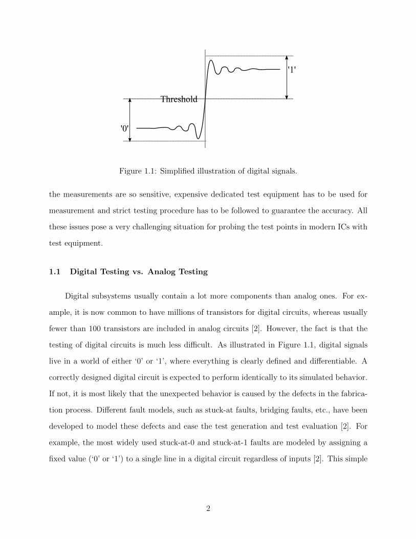
Figure 1.1: Simplified illustration of digital signals.
the measurements are so sensitive, expensive dedicated test equipment has to be used for
measurement and strict testing procedure has to be followed to guarantee the accuracy. All
these issues pose a very challenging situation for probing the test points in modern ICs with
test equipment.
1.1 Digital Testing vs. Analog Testing
Digital subsystems usually contain a lot more components than analog ones. For ex-
ample, it is now common to have millions of transistors for digital circuits, whereas usually
fewer than 100 transistors are included in analog circuits [2]. However, the fact is that the
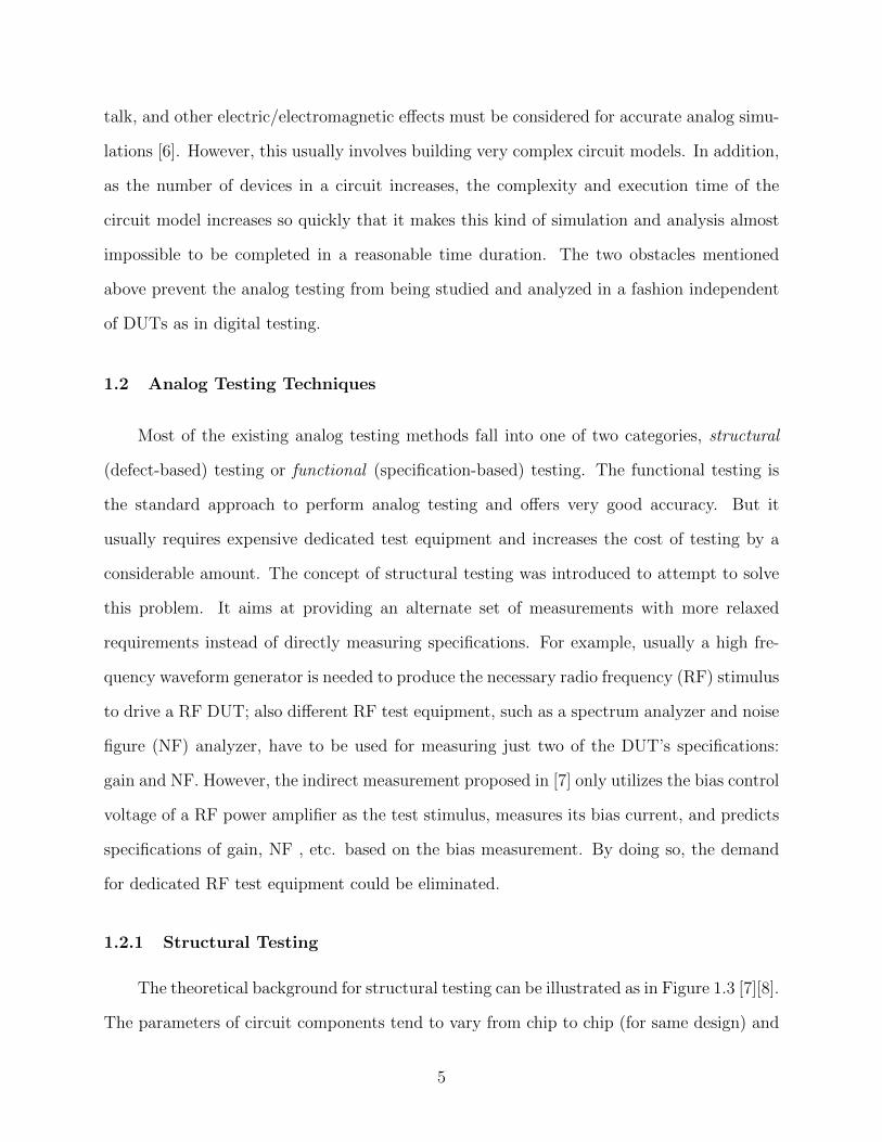
testing of digital circuits is much less difficult. As illustrated in Figure 1.1, digital signals
live in a world of either ‘0’ or ‘1’, where everything is clearly defined and differentiable. A
correctly designed digital circuit is expected to perform identically to its simulated behavior.
If not, it is most likely that the unexpected behavior is caused by the defects in the fabrica-
tion process. Different fault models, such as stuck-at faults, bridging faults, etc., have been
developed to model these defects and ease the test generation and test evaluation [2]. For
example, the most widely used stuck-at-0 and stuck-at-1 faults are modeled by assigning a
fixed value (‘0’ or ‘1’) to a single line in a digital circuit regardless of inputs [2]. This simple
2
fault model allows us to inject faults into the gate-level description of a digital circuit, to ap-
ply different test vectors to the circuit in behavior simulation (a.k.a. fault simulation in this
context), to evaluate the fault coverage of the applied vectors, and to choose the vector with
best fault coverage for circuit testing. The introduction of automatic test pattern generation
(ATPG) algorithms even eliminates the necessity of human involvement and automates the
process of searching test vectors [2][3].
In order to overcome the issues of limited observability and controllability in devices
under test (DUTs) , the concept of scan test has been developed and widely adopted in
digital testing. By replacing regular D flip-flops (DFFs) with scan flip-flops (SFFs), the
flip-flops (FFs) at the critical test points can be connected together to form a scan chain [4].
In the normal mode, every SFF works as a regular DFF. However, in the scan mode, a test
vector could be shifted into the scan chain bit by bit. Once all the data is shifted in and
the test vector is ready, the SFFs are switched to the normal mode. After a certain number
of clock cycles, the SFFs will then be switched to the scan mode and the internal signals
captured by the SFFs could be shifted out of the DUT bit by bit. The scan test employs just
four I/Os, three primary inputs (PIs) and one primary output (PO) , and makes it possible
to manipulate and monitor any number of critical nodes, where FFs reside, in a circuit.
It is because of the well-developed fault models and matured behavior simulation that the
test generation for a digital DUT can be developed independently regardless of functional
behavior of the DUT. This methodology proves to be very effective for testing digital circuits,
therefore, the concepts of ATPG and design for test (DFT) have been incorporated into the
standard digital IC design flow and widely supported by various CAD tools.
The testing of analog ICs, however, has fallen far behind and is typically performed
manually. There are several reasons responsible for the difficulties encountered in the analog
testing. First, the efficiency of the analog circuits comes from the complex nature of the
analog signals on both time and amplitude. Unlike the digital domain where only pulse
3
t
x(t)
DC
Off
set
Vpp
Peroid
Initi
al P
hase
digital code
output voltage
Nonlinearity in DAC
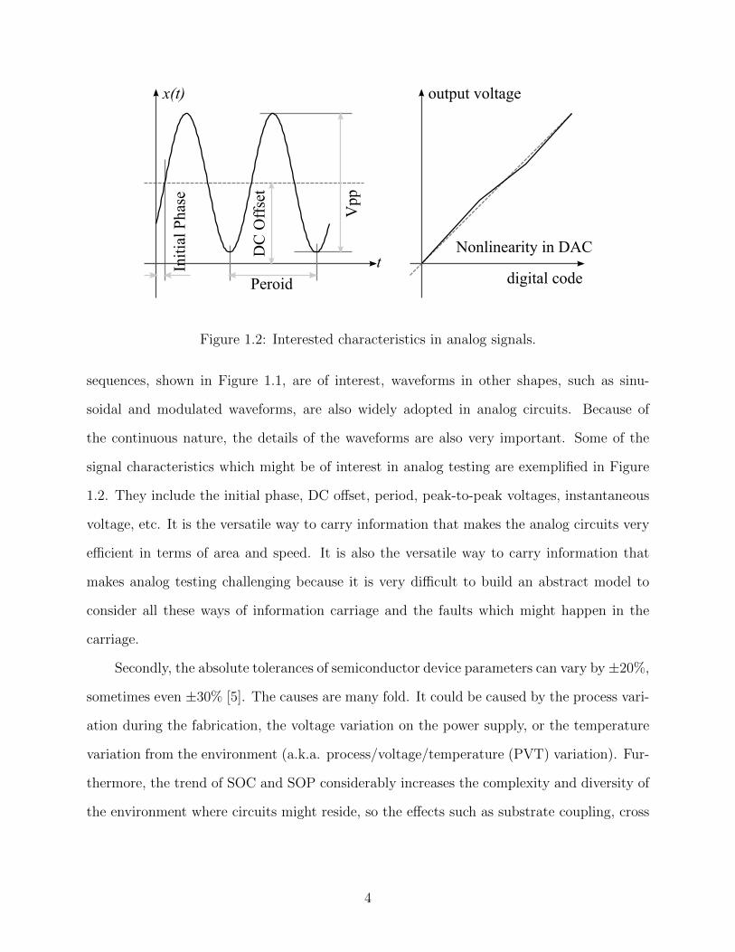
Figure 1.2: Interested characteristics in analog signals.
sequences, shown in Figure 1.1, are of interest, waveforms in other shapes, such as sinu-
soidal and modulated waveforms, are also widely adopted in analog circuits. Because of
the continuous nature, the details of the waveforms are also very important. Some of the
signal characteristics which might be of interest in analog testing are exemplified in Figure
1.2. They include the initial phase, DC offset, period, peak-to-peak voltages, instantaneous
voltage, etc. It is the versatile way to carry information that makes the analog circuits very
efficient in terms of area and speed. It is also the versatile way to carry information that
makes analog testing challenging because it is very difficult to build an abstract model to
consider all these ways of information carriage and the faults which might happen in the
carriage.
Secondly, the absolute tolerances of semiconductor device parameters can vary by±20%,
sometimes even ±30% [5]. The causes are many fold. It could be caused by the process vari-
ation during the fabrication, the voltage variation on the power supply, or the temperature
variation from the environment (a.k.a. process/voltage/temperature (PVT) variation). Fur-
thermore, the trend of SOC and SOP considerably increases the complexity and diversity of
the environment where circuits might reside, so the effects such as substrate coupling, cross
4
talk, and other electric/electromagnetic effects must be considered for accurate analog simu-
lations [6]. However, this usually involves building very complex circuit models. In addition,
as the number of devices in a circuit increases, the complexity and execution time of the
circuit model increases so quickly that it makes this kind of simulation and analysis almost
impossible to be completed in a reasonable time duration. The two obstacles mentioned
above prevent the analog testing from being studied and analyzed in a fashion independent
of DUTs as in digital testing.
1.2 Analog Testing Techniques
Most of the existing analog testing methods fall into one of two categories, structural
(defect-based) testing or functional (specification-based) testing. The functional testing is
the standard approach to perform analog testing and offers very good accuracy. But it
usually requires expensive dedicated test equipment and increases the cost of testing by a
considerable amount. The concept of structural testing was introduced to attempt to solve
this problem. It aims at providing an alternate set of measurements with more relaxed
requirements instead of directly measuring specifications. For example, usually a high fre-
quency waveform generator is needed to produce the necessary radio frequency (RF) stimulus
to drive a RF DUT; also different RF test equipment, such as a spectrum analyzer and noise
figure (NF) analyzer, have to be used for measuring just two of the DUT’s specifications:
gain and NF. However, the indirect measurement proposed in [7] only utilizes the bias control
voltage of a RF power amplifier as the test stimulus, measures its bias current, and predicts
specifications of gain, NF , etc. based on the bias measurement. By doing so, the demand
for dedicated RF test equipment could be eliminated.
1.2.1 Structural Testing
The theoretical background for structural testing can be illustrated as in Figure 1.3 [7][8].
The parameters of circuit components tend to vary from chip to chip (for same design) and
5
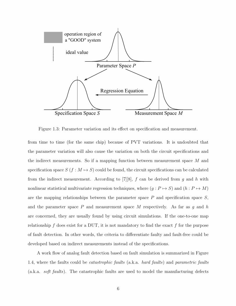
Parameter Space P
Specification Space S Measurement Space M
Regression Equation
operation region of a "GOOD" system
ideal value
Figure 1.3: Parameter variation and its effect on specification and measurement.
from time to time (for the same chip) because of PVT variations. It is undoubted that
the parameter variation will also cause the variation on both the circuit specifications and
the indirect measurements. So if a mapping function between measurement space M and
specification space S (f : M 7→ S) could be found, the circuit specifications can be calculated
from the indirect measurement. According to [7][8], f can be derived from g and h with
nonlinear statistical multivariate regression techniques, where (g : P 7→ S) and (h : P 7→M)
are the mapping relationships between the parameter space P and specification space S,
and the parameter space P and measurement space M respectively. As far as g and h
are concerned, they are usually found by using circuit simulations. If the one-to-one map
relationship f does exist for a DUT, it is not mandatory to find the exact f for the purpose
of fault detection. In other words, the criteria to differentiate faulty and fault-free could be
developed based on indirect measurements instead of the specifications.
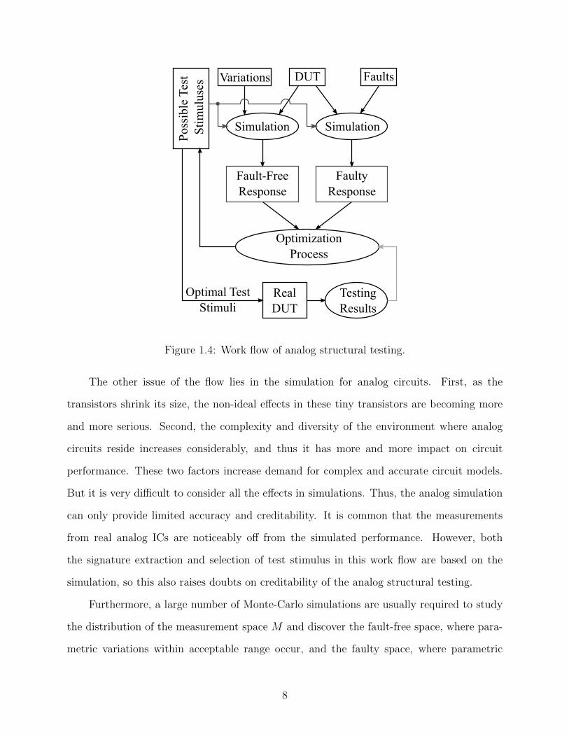
A work flow of analog fault detection based on fault simulation is summarized in Figure
1.4, where the faults could be catastrophic faults (a.k.a. hard faults) and parametric faults
(a.k.a. soft faults). The catastrophic faults are used to model the manufacturing defects
6
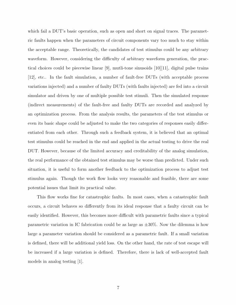
which fail a DUT’s basic operation, such as open and short on signal traces. The paramet-
ric faults happen when the parameters of circuit components vary too much to stay within
the acceptable range. Theoretically, the candidates of test stimulus could be any arbitrary
waveform. However, considering the difficulty of arbitrary waveform generation, the prac-
tical choices could be piecewise linear [9], mutli-tone sinusoids [10][11], digital pulse trains
[12], etc.. In the fault simulation, a number of fault-free DUTs (with acceptable process
variations injected) and a number of faulty DUTs (with faults injected) are fed into a circuit
simulator and driven by one of multiple possible test stimuli. Then the simulated response
(indirect measurements) of the fault-free and faulty DUTs are recorded and analyzed by
an optimization process. From the analysis results, the parameters of the test stimulus or
even its basic shape could be adjusted to make the two categories of responses easily differ-
entiated from each other. Through such a feedback system, it is believed that an optimal
test stimulus could be reached in the end and applied in the actual testing to drive the real
DUT. However, because of the limited accuracy and creditability of the analog simulation,
the real performance of the obtained test stimulus may be worse than predicted. Under such
situation, it is useful to form another feedback to the optimization process to adjust test
stimulus again. Though the work flow looks very reasonable and feasible, there are some
potential issues that limit its practical value.
This flow works fine for catastrophic faults. In most cases, when a catastrophic fault
occurs, a circuit behaves so differently from its ideal response that a faulty circuit can be
easily identified. However, this becomes more difficult with parametric faults since a typical
parametric variation in IC fabrication could be as large as ±30%. Now the dilemma is how
large a parameter variation should be considered as a parametric fault. If a small variation
is defined, there will be additional yield loss. On the other hand, the rate of test escape will
be increased if a large variation is defined. Therefore, there is lack of well-accepted fault
models in analog testing [1].
7
DUT Faults
SimulationSimulation
Pos
sibl
e Te
st S
tim
ulus
es
Fault-Free Response
FaultyResponse
OptimizationProcess
RealDUT
TestingResults
Optimal Test Stimuli
Variations
Figure 1.4: Work flow of analog structural testing.
The other issue of the flow lies in the simulation for analog circuits. First, as the
transistors shrink its size, the non-ideal effects in these tiny transistors are becoming more
and more serious. Second, the complexity and diversity of the environment where analog
circuits reside increases considerably, and thus it has more and more impact on circuit
performance. These two factors increase demand for complex and accurate circuit models.
But it is very difficult to consider all the effects in simulations. Thus, the analog simulation
can only provide limited accuracy and creditability. It is common that the measurements
from real analog ICs are noticeably off from the simulated performance. However, both
the signature extraction and selection of test stimulus in this work flow are based on the
simulation, so this also raises doubts on creditability of the analog structural testing.
Furthermore, a large number of Monte-Carlo simulations are usually required to study
the distribution of the measurement space M and discover the fault-free space, where para-
metric variations within acceptable range occur, and the faulty space, where parametric
8
faults happen. These simulations usually require considerable execution time and raise an-
other issue of analog structural testing — efficiency. Because of these issues, structural
testing is not widely used in industry although it has received considerable attention from
researchers in literature [13][14][15][16][17].
1.2.2 Functional Testing
Functional testing is also known as specification-based testing and widely employed in
industry. It directly measures the performance merits of DUTs, compares the measurement
results against well-defined specifications, and identifies the faulty circuits if they fall outside
of provided tolerance limits. Because the functional testing is done against specifications,
it usually guarantees very high test accuracy. However, this method is usually performed
manually with expensive test equipment and sometimes strict testing procedures have to be
followed to capture accurate measurement results. Furthermore, some pieces of the equip-
ment are dedicated for very limited measurements and oftentimes different equipments have
to be used to fully characterize one DUT. Therefore, the traditional methodology of manual
functional testing is more and more costly and time consuming. For example, the RF IC
test cost could be as high as 50% of the total cost, depending on the complexity of the func-
tionality to be tested [10]. Therefore, it becomes attractive to automate the testing process
with low-cost and built-in self-test (BIST) circuitry. It is also most effective to consider
testing in the product cycle as early as possible [2]. Although it is inevitable that the BIST
circuity will bring some resource overhead to a system, with properly designed BIST, the
cost of added test hardware will be more than compensated for by the benefits in terms of
reliability and the reduced testing and maintenance cost [18].
1.2.3 Analog and Mixed-Signal Built-In Self-Test
Though the BIST technology is well developed and adopted for digital circuits, BIST
dedicated for analog circuits is still in its early stage. A few BIST techniques have been
9
proposed to perform the on-chip analog testing [1]. Most of the analog and mixed-signal
BIST approaches fall into the following two categories: intrusive and non-intrusive. The
intrusive BIST requires mandatory modifications to DUTs while the non-intrusive BIST
leaves the DUTs untouched.
Intrusive BIST
The intrusive BIST approaches need to modify the original topology of a DUT for the
purpose of monitoring or mode control. The current-based RF BIST approach proposed in [6]
inserts a current sensor in the DUT’s bias network, monitors the bias current, and analyzes
the current signature to tell if catastrophic or parametric faults happen in the DUT. A similar
approach was proposed in [19] and uses a built-in current sensor to measure IDDQ for defect
detection. In addition to current, other signals in DUTs can also be measured to test devices.
For example, by inserting a test amplifier and two RF peak detectors, [20] claims to be able
to utilize input impedance and DC voltage measurement to extract gain, noise figure, input
impedance, and input return loss of a low noise amplifier (LNA). However, it is believed
that this approach has very little practical applicability due to the massive overheads and
significant intrusion on the DUT [6].
Another well-known family of intrusive BIST is the oscillation BIST (OBIST). This
approach was first proposed in [21]. With OBIST, an analog DUT has two working modes
— normal and test mode, and is able to switch between the modes through external controls.
The DUT acts as usual in normal mode; however, during test mode, the DUT is reconfigured
to form an oscillator and its oscillation frequency exhibits a strong dependence on various
parameters of the circuit components involved in the oscillator. In other words, the DUT’s
circuit parameters can be estimated based on the oscillation frequency and thus used for
fault detection. However, because there is no universal methodology to transform a DUT
into an oscillator, the effort of building OBIST with minimal modifications is not trivial.
10
It is obvious that the intrusive BIST approaches require no on-chip test pattern gen-
erator (TPG) and thus can be implemented with small hardware overhead. However, they
modify the original topology of the DUT to perform indirect measurements of DC current,
DC voltage, oscillation frequency, etc., which could be captured with much looser require-
ments. Therefore, essentially the intrusive BIST approaches are on-chip implementations of
structural testing, thus a number of fault simulations are required to extract the measure-
ment space and build the relationship between the indirect measurements and the possible
catastrophic or parametric faults. Furthermore, the mandatory modifications to the original
circuit structure may also cause undesired performance variations.
Non-Intrusive BIST
The non-intrusive BIST applies no modifications to DUTs and usually incorporates a
test pattern generator (TPG) and an output response analyzer (ORA) . The former produces
the necessary test stimulus to drive a DUT and the latter analyzes the output of the DUT
to tell whether the DUT is faulty or fault-free.
An on-chip ramp generator was proposed in [22] for measuring the nonlinearity of analog-
to-digital converters (ADCs). Linear ADCs are supposed to produce a linearly increasing
digital output to represent a linearly increasing analog input. However, real ADCs always
introduce errors in the process of conversion and causes nonlinearity. Integral nonlinearity
(INL) and differential nonlinearity (DNL) are two of the most important specifications for
ADCs and a linear stimulus are usually required for measuring them [23]. The on-chip ramp
generator provides a BIST alternative for these measurements. However, the measurement
accuracy is greatly limited by the linearity of the on-chip ramp generator [10].
While applying an impulse to a linear, time invariant (LTI) system, the system output is
the system transfer function which fully characterizes the system’s dynamic behavior. Thus,
impulse response based testing has been utilized in [24][25]. The on-chip impulse generation
11
was suggested in [26] to test analog DUTs. It greatly simplifies the circuit complexity for gen-
erating test stimulus; however, it requires analog fault models and Monte-Carlo simulations
to extract the signatures of faulty and fault-free DUTs.
The mixed-signal BIST approach given in [17] provides a variety of test waveforms and
utilizes different accumulation modes for fault detection of a wide range of analog circuits.
Its TPG is able to produce test waveforms of saw-tooth, reverse saw-tooth, triangular wave,
pseudo-random, DC, step, pulse, frequency sweep, and ramp. The ORA uses the final sum
in its accumulator as the DUT’s signature. By comparing the extracted signature with a
predefined range of values, the DUT’s pass/fail status can be determined. Because this
approach is based on structural testing, it has the similar issues as fault models and fault
simulation.
In order to perform a suite of analog functionality tests, such as frequency response,
linearity, harmonic spur, signal-to-noise ratio (SNR) and NF measurements in a BIST envi-
ronment, the frequency spectrum of the DUT’s output response needs to be measured by an
ORA. Reference [27] utilizes an fast Fourier transform (FFT) processor to perform on-chip
spectrum analysis. However, given a digital input with N samples, an FFT processor re-
quires around N log2(N) multipliers and adders [28]. Such a prohibitive hardware overhead
and power consumption prevent it from being an efficient BIST unless the FFT is an inherent
component of the system.
In contrast, analog spectrum analysis techniques try to perform the spectrum analysis
in the analog domain and could be implemented with much less hardware overhead. The
switched-capacitor spectrum analyzer proposed in [29] employs a switched-capacitor sine
wave generator as the TPG and its ORA consists of a bandpass filter (BPF) , a variable gain
amplifier (VGA), and a ADC. Because of the limitations of the switched-capacitor TPG,
this BIST approach works at low frequency and is only able to measure spectrum at the
frequency of fundamental and harmonics. The multi-resolution spectrum sensing (MRSS)
technique proposed in [30] suggests correlating RF signals to time-frequency windows with
12
analog circuits. Since the windows are produced by digital window generator, it offers the
flexibility to control the type and duration of the windows and thus the ability of multi-
resolution of bandwidth. It is also reported in [31] that the RF power detector (RPD) was
employed to perform on-chip RF voltage measurement. Although these BIST approaches
offers very low area overhead, all of them suffer from limited dynamic range and coarse
frequency sweeping due to the nature of analog processing.
A fully digital selective spectrum analysis (SSA) technique was proposed in [10][32]. This
approach includes a direct digital synthesizer (DDS)-based TPG and multiplier/accumulator
(MAC)-based ORA and is capable of accurate frequency response, nonlinearity, spur search,
and SNR measurements. The ORA consists of two MACs where the DUT output is mul-
tiplied with an in-phase reference at the frequency under analysis and accumulated in one
MAC and a similar procedure occurs in the other MAC but with an out-of-phase reference.
Thus, the in-phase and out-of-phase components of the output at this frequency can be ex-
tracted and used for calculations of magnitude and phase. Because the signals are in digital
form, it can achieve very fine frequency resolution and provide accurate results with wide
dynamic range. Since the SSA only analyzes the spectrum of one frequency point at a time,
it can be implemented with much simpler circuitry than FFT-based BIST.
Other Benefits of BIST
The concept of the adaptive control has been known and studied for decades [33]. The
technology is mainly used in industrial systems whose critical parameters vary over time
or with environmental variations, such as temperature, external pressure, humidity, etc.
Its basic theory is to include an adaptive controller in a time-varying or environmentally
sensitive system which can monitor the performance of the system and adjust it accordingly
such that the performance variation can be diminished to an acceptable or even negligible
level. However, its applications were restricted by the intensive computation required for
adaptive control algorithms.
13
System
BISTCircuitry
TunableCircuitry
input output
Figure 1.5: General model of an adaptive mixed-signal system with BIST technology.
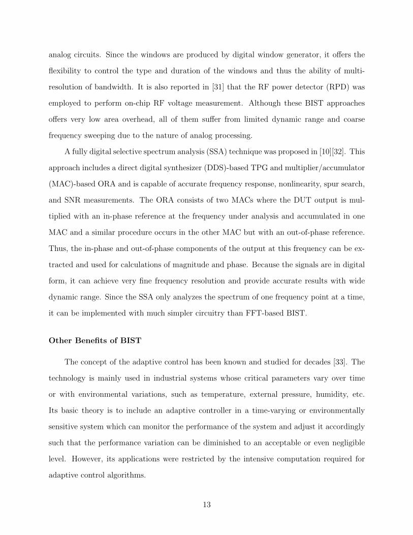
The advance of BIST technology provides a system not only the capability to test
itself, but also an efficient means for calibrating, compensating, and adjusting the analog
circuitry adaptively [10][32]. It is more than appropriate to be applied in a mixed-signal
system with supports for adaptive control. The general model of an adaptive mixed-signal
system built with the proposed BIST technology is illustrated in Figure 1.5. First the
BIST circuitry captures the system output, through which the critical parameters of the
system performance are determined in real time. Then the built-in tunable circuitry, such as
capacitor banks, resistor banks, etc., will be adjusted according to the measurement results,
such that the system variations could be compensated correspondingly. For example, if
the cut-off frequency of the system deviates from the expected value, another capacitor in
the capacitor bank can be activated to stabilize the cut-off frequency. If the linearity of a
system is degraded because of increased interference or signal strength, the bias current of
an amplifier in the system can be adjusted accordingly in the tunable circuitry. However, the
key factor which determines the performance of an adaptive system, illustrated in Figure 1.5,
is to accurately measure the functional parameters of the system with the BIST circuitry.
Recently more and more field programmable gate arrays (FPGAs) are adopted in var-
ious mixed-signal systems for their ability to be reconfigured in the field to implement a
desired function according to the real-time demands. Furthermore, with FPGAs in the digi-
tal portion of a mixed-signal system, the FPGA can be reconfigured with the BIST circuitry
only when needed for analog test and measurement; otherwise, the normal system function
14
would reside in the FPGA such that there is no area or performance penalty associated with
the BIST circuitry.
1.3 Organization of the Dissertation
In this dissertation, we will investigate and discuss the design and implementation of
the proposed SSA-based mixed-signal BIST in detail. This proposed BIST architecture
has the ability to drive an analog DUT with one-tone or two-tone stimulus and conduct
spectrum analysis on the DUT’s output. Therefore, it is able to perform a suite of analog
measurements, such as frequency response, nonlinearity, etc.. The dissertation is organized
as follows. Chapter 2 briefly presents the spectrum-based analog specifications and the basic
architecture of the SSA-based BIST. In Chapter 3, the theoretical background of the SSA-
based ORA and its equivalency to FFT is studied; then the proposed integer multiple period
(IMP) accumulations for different analog measurements and the performance improvement
in terms of test time and accuracy are investigated. In Chapter 4, one of the most important
components, the numerically controlled oscillator (NCO), and the coordinate rotation digital
computer (CORDIC) algorithm for its implementation is explored in depth. Finally, the
dissertation is concluded with remarks in Chapter 5.
15

Chapter 2
Overview to Spectrum-Based Analog Testing
While analyzing a system, it is common to assume the system as an LTI system be-
cause a LTI system has some very attractive features. First, a LTI system can be fully
characterized by its response while applying an impulse to its input. That is also why the
impulse response is called the system transfer function. Second, the system response with
any arbitrary input can be calculated from the convolution of the input to the system trans-
fer function. However, this assumption does not always hold true for analog circuits. Both
the metal-oxide-semiconductor field-effect transistors (MOSFETs) and bipolar transistors
exhibit strong nonlinear behaviors with respect to their input voltage (gate-source voltage
for MOSFETs and base-emitter voltage for bipolar transistors) in their active region. The
former supplies a drain current which is the square function of its gate-source voltage, while
the latter does a collector current which is the exponential function of its base-emitter volt-
age. In order to simplify the complexity of the circuit analysis, the concept of small signal
was introduced to neglect the transistor’s nonlinear effects and approximate the transistor’s
operation with linear models. However, in reality, the nonlinearity of transistors still exists
and leads to some interesting and important phenomena happening in analog DUTs.
Furthermore, the reactive components are everywhere in analog circuits. They could be
on-chip capacitors, inductors, or even the parasitic capacitance coming from the integrated
components such as transistors, resistors, metal traces, etc. All these components make ana-
log DUTs behave differently at different frequencies because their impedance heavily depends
on the frequency. Though they do not demand power consumption, the charging/discharging
cycles of these devices introduces frequency-dependent delays to analog DUTs. Therefore,
16
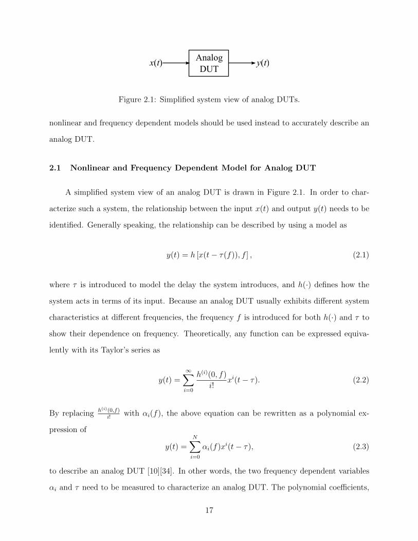
Analog DUT
x(t) y(t)
Figure 2.1: Simplified system view of analog DUTs.
nonlinear and frequency dependent models should be used instead to accurately describe an
analog DUT.
2.1 Nonlinear and Frequency Dependent Model for Analog DUT
A simplified system view of an analog DUT is drawn in Figure 2.1. In order to char-
acterize such a system, the relationship between the input x(t) and output y(t) needs to be
identified. Generally speaking, the relationship can be described by using a model as
y(t) = h [x(t− τ(f)), f ] , (2.1)
where τ is introduced to model the delay the system introduces, and h(·) defines how the
system acts in terms of its input. Because an analog DUT usually exhibits different system
characteristics at different frequencies, the frequency f is introduced for both h(·) and τ to
show their dependence on frequency. Theoretically, any function can be expressed equiva-
lently with its Taylor’s series as
y(t) =∞∑i=0
h(i)(0, f)
i!xi(t− τ). (2.2)
By replacing h(i)(0,f)i!
with αi(f), the above equation can be rewritten as a polynomial ex-
pression of
y(t) =N∑i=0
αi(f)xi(t− τ), (2.3)
to describe an analog DUT [10][34]. In other words, the two frequency dependent variables
αi and τ need to be measured to characterize an analog DUT. The polynomial coefficients,
17
αi, carry some of the most interesting physical properties of the DUT. For example, DC
offset and gain are given by α0 and α1 respectively; αi(i > 1) are introduced to model the
nonlinearity of the DUT. The other variable τ describes the delay caused by the DUT at
different frequencies. For simplicity purpose, oftentimes N = 3 is sufficient to accurately
describe an analog DUT.
Because both αi and τ are frequency dependent, Equation (2.3) could be quite com-
plicated if the input x(t) is a wide-band signal. Usually multi-tone sinusoidal signals are
applied to analog DUTs for testing because these signals just concentrate their energy at
several frequency points. By doing so, Equation (2.3) becomes much simpler such that the
interested information could be extracted with much less effort. A multi-tone stimulus could
be expressed as
x(t) =∑j
Bj cos(2πfjt+ θj), (2.4)
where Bj, fj, and θj is the amplitude, frequency, and initial phase of the j-th tone. Substitut-
ing x(t) in Equation (2.3) with Equation (2.4), the DUT’s output, y(t), can be approximately
given as
y(t) ≈ α0 + α1
∑j
Bj cos[2πfj(t− τ) + θj] +
α2
(∑j
Bj cos[2πfj(t− τ) + θj]
)2
+
α3
(∑j
Bj cos[2πfj(t− τ) + θj]
)3
, (2.5)
if the 4th and higher order terms are neglected. Therefore, not only does the output, y(t),
appear at the input fundamental frequencies, but also the inter-modulation (IM) frequencies
introduced by the 2nd and 3rd order terms. For simplicity, Equation (2.5) can be expressed
in its equivalent form
y(t) =M∑k=0
Ak cos(2πfkt+ ∆φk), (2.6)
18
where Ak and ∆φk are the magnitude and phase of the output at frequency fk, which could
be any possible fundamental and IM frequencies. Therefore, the DUT’s output spectrum
has to be analyzed to find all the possible pairs of (Ak, ∆φk) at frequency fk to characterize
a DUT.
2.2 Spectrum-Based Specifications
In analog functional testing, usually only 1-tone or 2-tone stimuli are used to evaluate a
circuit’s specifications to ease the effort of test stimuli generation. By using these stimuli, it
is possible to measure a number of specifications, including frequency response, nonlinearity,
harmonic spurs, SNR, NF, etc.
2.2.1 Single-Tone Specifications
When a single-tone signal x(t) = B cos(2πft + θ) is applied, the system output y(t)
could be calculated from Equation (2.5) as
y(t) ≈ α0 + α1B cos[2πf(t− τ) + θ] + α2B2 cos2[2πf(t− τ) + θ] +
α3B3 cos3[2πf(t− τ) + θ]. (2.7)
Based on the above equation, the following information, including frequency response, P1dB
point, noise and spurs, could be extracted.
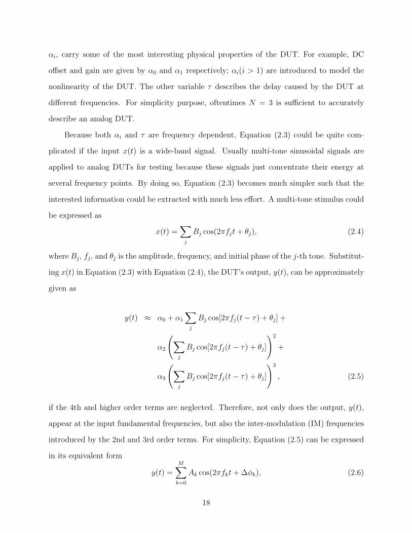
Frequency Response
If the system input x(t) is a small signal, its amplitude B is a small quantity and thus
B3 << B2 << B. Based on this conclusion, we find out that the third and four terms in
Equation (2.7) become negligible in comparison with the second term. Therefore, the system
19
Frequency
Spe
ctru
m M
agni
tude
Amplitude Response
Sin
gle-
Tone
Sig
nal
Frequency Sweeping over Bandwidth
Figure 2.2: Illustration of frequency spectrum measurement with single-tone test.
output y(t) can be further approximated as
y(t) ≈ α0 + α1B cos[2πf(t− τ(f)) + θ]. (2.8)
From Equation (2.8), it can be observed that only the fundamental frequency component
from the second term presents itself besides the DC offset α0. So the output spectrum (A,
∆φ) at frequency f can be expressed as
A(f)[dB] = 20 log10[α1(f)] [dB] + 20 log10B [dB], (2.9a)
∆φ(f) = θ − 2πfτ(f). (2.9b)
Because B and θ are the amplitude and phase of the input signal respectively, B and
θ can be estimated by monitoring the input spectrum at frequency f . Bring the estimated
B and θ back in Equation (2.9), the DUT’s frequency response, including the magnitude
α1(f) and phase response 2πfτ(f), at the frequency f can be calculated based on the output
spectrum A(f) and ∆φ(f). As shown in Figure 2.2, by sweeping the frequency f over the
band of interest and also calculating the spectrum difference between the DUT’s input and
20
output at each frequency, the magnitude response α1 and phase response 2πfτ over the
interested bandwidth can be characterized.
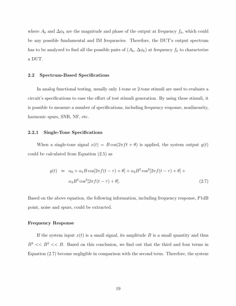
1dB Gain Compression Point
If the single-tone input x(t) = B cos(2πft+ θ) is fairly large, it is not true that B3 <<
B2 << B. When this happens, the third and fourth terms in Equation (2.7) are not negligible
any more and they can be rewritten as
α2B2 cos2(2πf(t− τ) + θ) =
α2B2
2{1 + cos[2π · 2f(t− τ(2f)) + 2θ]} , (2.10a)
α3B3 cos3(2πf(t− τ) + θ) =
α3B3
4{3 cos[2πf(t− τ(f)) + θ] +
cos[2π · 3f(t− τ(3f)) + 3θ]}. (2.10b)
By putting Equation (2.10) back into Equation (2.7), it is not hard to notice that the
output spectrum appears at both the fundamental frequency f and its harmonics 2f and
3f . Furthermore, the spectrum at f does not solely come from the first term in Equation
(2.7), but also the third term according to Equation (2.10b). Therefore, the output spectrum
magnitude at f , A(f), can be derived as
A(f)[dB] = 20 log10
[α1(f) +
3
4α3(f)B2
][dB] + 20 log10B [dB]. (2.11)
For most of analog DUTs, their outputs are “compressive” or “saturating” functions
of their inputs [34]; in other words, the gain α1(f) + 34α3(f)B2 becomes smaller as the
input amplitude B grows stronger. This phenomenon happens only if α3 is negative. A clear
illustration of this effect is drawn in Figure 2.3, where the input and output signal strength, B
and A(f), are plotted with dB scale. From Figure 2.3, we can see that the amplification gain
is weaker though the output still keeps increasing as input power increases. When the gain
is 1-dB smaller than its small-signal gain α1(f), the input signal strength, 20 log10B [dB], at
21
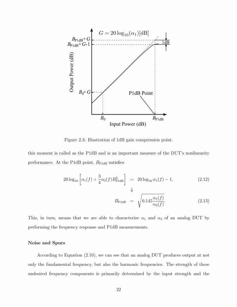
Input Power (dB)B0 BP1dB
Out
put P
ower
(dB
)
B +G0
B +GP1dB 1dB
P1dB Point
B +G-1P1dB
Figure 2.3: Illustration of 1dB gain compression point.
this moment is called as the P1dB and is an important measure of the DUT’s nonlinearity
performance. At the P1dB point, BP1dB satisfies
20 log10
[α1(f) +
3
4α3(f)B2
P1dB
]= 20 log10 α1(f)− 1, (2.12)
⇓
BP1dB =
√0.145
α1(f)
α3(f). (2.13)
This, in turn, means that we are able to characterize α1 and α3 of an analog DUT by
performing the frequency response and P1dB measurements.
Noise and Spurs
According to Equation (2.10), we can see that an analog DUT produces output at not
only the fundamental frequency, but also the harmonic frequencies. The strength of these
undesired frequency components is primarily determined by the input strength and the
22
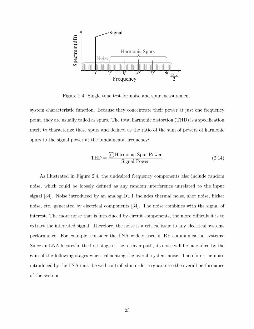
Frequencyfclk2
Spe
ctru
m(d
B)
f 2f 3f
Harmonic Spurs
4f 5f 6f
Noise
Signal
Figure 2.4: Single tone test for noise and spur measurement.
system characteristic function. Because they concentrate their power at just one frequency
point, they are usually called as spurs. The total harmonic distortion (THD) is a specification
merit to characterize these spurs and defined as the ratio of the sum of powers of harmonic
spurs to the signal power at the fundamental frequency:
THD =
∑Harmonic Spur Power
Signal Power. (2.14)
As illustrated in Figure 2.4, the undesired frequency components also include random
noise, which could be loosely defined as any random interference unrelated to the input
signal [34]. Noise introduced by an analog DUT includes thermal noise, shot noise, flicker
noise, etc. generated by electrical components [34]. The noise combines with the signal of
interest. The more noise that is introduced by circuit components, the more difficult it is to
extract the interested signal. Therefore, the noise is a critical issue to any electrical systems
performance. For example, consider the LNA widely used in RF communication systems.
Since an LNA locates in the first stage of the receiver path, its noise will be magnified by the
gain of the following stages when calculating the overall system noise. Therefore, the noise
introduced by the LNA must be well controlled in order to guarantee the overall performance
of the system.
23
There are two important specifications widely used to characterize the noise. One is the
SNR, which is defined as
SNR =Signal Power
Noise Power in Interested Bandwidth(2.15)
Alternatively, the noise added in a circuit can be characterized using the NF, which is defined
as
NF =SNRin
SNRout
(2.16)
where SNRin and SNRout are the SNRs measured at the input and output of the DUT
respectively [34]. It is also common to consider the noise and spurs together because both
of them are undesired and deteriorate the signal quality at the output of an analog DUT.
The total harmonic distortion plus noise, THD+N, is defined for such purpose and given as
THD+N =
∑Harmonic Spur Power + Noise Power
Signal Power, (2.17)
whose multiplicative inverse is also known as signal-to-noise and distortion (SINAD) .
The measurement of noise is usually performed in the frequency domain instead of the
time domain mainly due to the following two factors. First, it is very difficult to differentiate
signal, noise, and spurs and find out their power in time domain. On the contrary, they
are well spread out in the frequency domain as shown in Figure 2.4 such that the interested
signal and other undesired frequency components can be easily differentiated. This is the
primary reason why the frequency domain is chosen for noise measurement. Second, even if it
is possible to determine the signal and noise power in the time domain, it is still meaningless
because we only care about the noise over the bandwidth of interest, which is usually much
smaller than the total noise presented in the time domain [2][34].
24
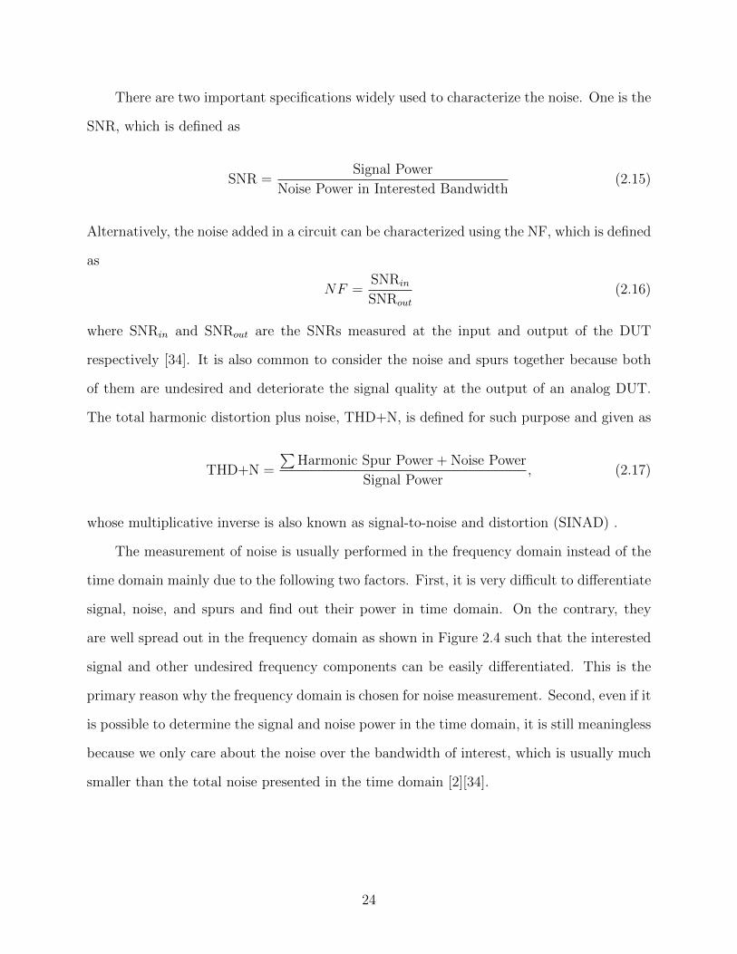
Two-Tone Input Spectrum
DUT
Output Spectrum
f1 f2
f1 f22f -f1 2 2f -f2 1
Pin
ΔP
0 1f -f2 2f1 2f2f +f1 2
Figure 2.5: Intermodulation in analog DUTs with two-tone stimulus.
2.2.2 Two-Tone Specification
When a two-tone signal x(t) = B [cos(2πf1t+ θ1) + cos(2πf2t+ θ2)] is applied at an
analog DUT’s input, the output y(t) can be approximated with
y(t) ≈ α0 + α1B {cos[2πf1(t− τ) + θ1] + cos[2πf2(t− τ) + θ2]}+
α2B2 {cos[2πf1(t− τ) + θ1] + cos[2πf2(t− τ) + θ2]}2 +
α3B3 {cos[2πf1(t− τ) + θ1] + cos[2πf1(t− τ) + θ1]}3 . (2.18)
The expansion of the square and cubic terms at the left side of the above equation
indicates the output has its spectrum contents not only the fundamental frequencies, but also
their harmonics and IM frequencies, as demonstrated in Figure 2.5. Of all these undesired
frequency components, the two third-order IM frequencies, 2f1 − f2 and 2f2 − f1 are of
particular interest. The reason is that these two frequencies are located in a close-in range
25

of the fundamental frequencies, f1 and f2, if f1 and f2 are closed spaced. This makes these
two IM terms very hard to remove because it is difficult to design a filter with a very sharp
transition band. It should be noted that the rest of the harmonics and IM frequencies are
usually far away from the interested frequencies, f1 and f2, as shown in Figure 2.5. Thus,
much less effort will be involved to filter these undesired spectrum contents. For the sake of
simplicity, only the spectrum at f1, f2, 2f1− f2, and 2f2− f1 are derived and the results are
listed as followed:
A(f1) = A(f2) = α1B +9
4α3B
3, (2.19a)
A(2f1 − f2) = A(2f2 − f1) =3
4α3B
3. (2.19b)
If the two-tone input is small enough, B3 << B. When this occurs, Equation (2.19)
could be approximated and expressed on dB scale as
A(f1)[dB] = A(f2)[dB] ≈ 20 log10 α1(f) + 20 log10B [dB], (2.20a)
A(2f1 − f2)[dB] = A(2f2 − f1)[dB] = 20 log10
[3
4α3(f)
]+ 60 log10B [dB]. (2.20b)
According to Equation (2.20), the spectrum magnitude at the fundamental and third-
order IM frequencies increases as illustrated in Figure 2.6 when the input signal strength B
increases. From the figure, we can see that A(2f1 − f2) and A(2f2 − f1) curves increase 3
times faster than the A(f1) and A(f2) curves on the dB scale as B grows. If the two curves
keep growing at the same rates, they will end up intercepting with each other eventually
and the cross point is defined as the 3rd-order intercept point (IP3) . When the IP3 occurs,
the input power B and the output spectrum A(f), where f ∈ {f1, f2, 2f1 − f2, 2f2 − f1},
are called as the input IP3 (IIP3) and the output IP3 (OIP3) respectively. However, it
should be noted the IP3 point in Figure 2.6 is an imaginary point that only exists in theory.
The reason is that the assumption of Equation (2.20a) does not hold true when B is large
26
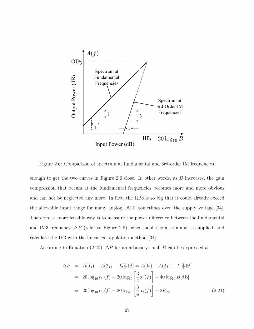
Figure 2.6: Comparison of spectrum at fundamental and 3rd-order IM frequencies.
enough to get the two curves in Figure 2.6 close. In other words, as B increases, the gain
compression that occurs at the fundamental frequencies becomes more and more obvious
and can not be neglected any more. In fact, the IIP3 is so big that it could already exceed
the allowable input range for many analog DUT, sometimes even the supply voltage [34].
Therefore, a more feasible way is to measure the power difference between the fundamental
and IM3 frequency, ∆P (refer to Figure 2.5), when small-signal stimulus is supplied, and
calculate the IP3 with the linear extrapolation method [34].
According to Equation (2.20), ∆P for an arbitrary small B can be expressed as
∆P = A(f1)− A(2f1 − f2)[dB] = A(f2)− A(2f2 − f1)[dB]
= 20 log10 α1(f)− 20 log10
[3
4α3(f)
]− 40 log10B[dB]
= 20 log10 α1(f)− 20 log10
[3
4α3(f)
]− 2Pin, (2.21)
27
where Pin = 20 log10B [dB]. At the IP3 point, the Equations (2.20a) and (2.20b) are equal
to each other. Therefore, the IIP3 satisfies
20 log10 α1(f) + IIP3 = 20 log10
[3
4α3(f)
]+ 3 · IIP3. (2.22)
⇓
IIP3 =1
2
{20 log10 α1(f)− 20 log10
[3
4α3(f)
]}. (2.23)
Bringing Equation (2.21) into Equation (2.23), we can see that IIP3 could be calculated
by using ∆P and Pin which are obtained for an arbitrary small B. The formula is given by
IIP3[dBm] =∆P [dB]
2+ Pin[dBm]. (2.24)
According to Equation (2.23), the input strength at IP3 point, BIP3, can be also calculated
as
BIP3 =
√4
3
α1(f)
α3(f). (2.25)
Both the IP3 and P1dB are the nonlinearity specifications for analog DUTs and they are
related to each other. By comparing Equation (2.13) and (2.25), the relationship between
IP3 and P1dB can be constructed as
BIP3
BP1dB
=
√4
0.145× 3≈ 3.0324, =⇒ IIP3 [dBm]− P1dB [dBm] ≈ 9.6dB. (2.26)
2.3 Architecture of Selective Spectrum Analysis-Based BIST
It is common for all the specification merits, such as frequency response, P1dB, SNR,
SINAD, IP3, etc., discussed in the Section 2.2 be measured with an analog DUT’s input and
output spectrum. Therefore, if a mixed-signal BIST has the ability to perform spectrum
analysis, it will be capable of measuring a wide range of specifications for analog DUTs.
The most well-known technique to do spectrum analysis is the FFT algorithm [28] and has
28
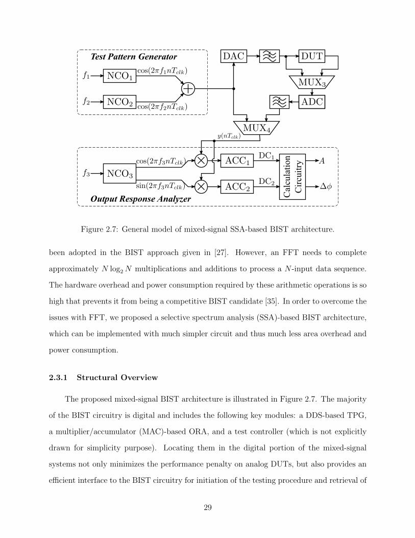
Test Pattern Generator
Output Response Analyzer Cal
cula
tion
Cir
cuitr
y
Figure 2.7: General model of mixed-signal SSA-based BIST architecture.
been adopted in the BIST approach given in [27]. However, an FFT needs to complete
approximately N log2N multiplications and additions to process a N -input data sequence.
The hardware overhead and power consumption required by these arithmetic operations is so
high that prevents it from being a competitive BIST candidate [35]. In order to overcome the
issues with FFT, we proposed a selective spectrum analysis (SSA)-based BIST architecture,
which can be implemented with much simpler circuit and thus much less area overhead and
power consumption.
2.3.1 Structural Overview
The proposed mixed-signal BIST architecture is illustrated in Figure 2.7. The majority
of the BIST circuitry is digital and includes the following key modules: a DDS-based TPG,
a multiplier/accumulator (MAC)-based ORA, and a test controller (which is not explicitly
drawn for simplicity purpose). Locating them in the digital portion of the mixed-signal
systems not only minimizes the performance penalty on analog DUTs, but also provides an
efficient interface to the BIST circuitry for initiation of the testing procedure and retrieval of
29

Phase Truancation
Phase toAmplitudeConversion
Mfull Mfull Mfull
Mfull
Mfull M
N
N
Phase Accumulator
FCW
NCOI
NCOQ
clk
Figure 2.8: A detailed view of the quadrature NCO in ORA.
subsequent results by a processor. The BIST architecture also utilizes the existing digital-
to-analog converters (DACs) and analog-to-digital converters (ADCs) typically associated
with most mixed-signal systems to provide a necessary interface between the digital BIST
and analog DUTs while minimizing the hardware added for BIST.
The other added test circuitry is the multiplexers (MUXs) which help build loop-back
capabilities for the test signals to return to the ORA. For example, in Figure 2.7, the MUX4
facilitates the testing and verification of the digital BIST circuitry prior to its use for testing
the analog BIST circuitry. The incorporation of MUX3 in the analog circuitry allows the
same to the DAC/ADC pair before the actual testing of analog DUTs. As a result, the
effects of the DAC and ADC can be factored out for more accurate measurements of DUTs.
Three numerically controlled oscillators (NCOs) are utilized in the proposed BIST. The
one used in the ORA is able to generate cosine and sine output simultaneously while the two
in TPG only produce a sine output. Figure 2.8 shows a more detailed view of the quadrature
NCO used in the ORA. The phase accumulator is used to generate the phase word based on
the frequency control word (FCW) input. The NCO utilizes a phase-to-amplitude conversion
unit to convert the truncated phase word sequence into a digital sinusoidal wave, whose
frequency can be determined as
fNCO =FCW · fclk
2Mfull(2.27)
30
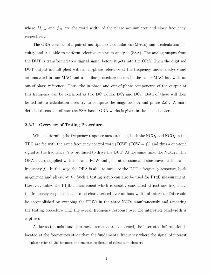
where Mfull and fclk are the word width of the phase accumulator and clock frequency,
respectively.
The ORA consists of a pair of multipliers/accumulators (MACs) and a calculation cir-
cuitry and it is able to perform selective spectrum analysis (SSA). The analog output from
the DUT is transformed to a digital signal before it gets into the ORA. Then the digitized
DUT output is multiplied with an in-phase reference at the frequency under analysis and
accumulated in one MAC and a similar procedure occurs in the other MAC but with an
out-of-phase reference. Thus, the in-phase and out-of-phase components of the output at
this frequency can be extracted as two DC values, DC1 and DC2. Both of these will then
be fed into a calculation circuitry to compute the magnitude A and phase ∆φ1. A more
detailed discussion of how the SSA-based ORA works is given in the next chapter.
2.3.2 Overview of Testing Procedure
While performing the frequency response measurement, both the NCO1 and NCO2 in the
TPG are fed with the same frequency control word (FCW) (FCW = f1) and thus a one-tone
signal at the frequency f1 is produced to drive the DUT. At the same time, the NCO3 in the
ORA is also supplied with the same FCW and generates cosine and sine waves at the same
frequency f1. In this way, the ORA is able to measure the DUT’s frequency response, both
magnitude and phase, at f1. Such a testing setup can also be used for P1dB measurement.
However, unlike the P1dB measurement which is usually conducted at just one frequency,
the frequency response needs to be characterised over an bandwidth of interest. This could
be accomplished by sweeping the FCWs in the three NCOs simultaneously and repeating
the testing procedure until the overall frequency response over the interested bandwidth is
captured.
As far as the noise and spur measurements are concerned, the interested information is
located at the frequencies other than the fundamental frequency where the signal of interest
1please refer to [36] for more implementation details of calculation circuitry
31
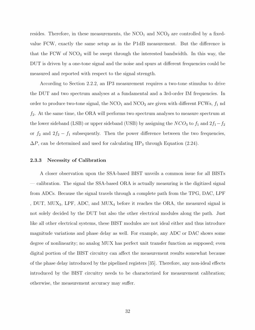
resides. Therefore, in these measurements, the NCO1 and NCO2 are controlled by a fixed-
value FCW, exactly the same setup as in the P1dB measurement. But the difference is
that the FCW of NCO3 will be swept through the interested bandwidth. In this way, the
DUT is driven by a one-tone signal and the noise and spurs at different frequencies could be
measured and reported with respect to the signal strength.
According to Section 2.2.2, an IP3 measurement requires a two-tone stimulus to drive
the DUT and two spectrum analyses at a fundamental and a 3rd-order IM frequencies. In
order to produce two-tone signal, the NCO1 and NCO2 are given with different FCWs, f1 nd
f2. At the same time, the ORA will performs two spectrum analyses to measure spectrum at
the lower sideband (LSB) or upper sideband (USB) by assigning the NCO3 to f1 and 2f1−f2
or f2 and 2f2 − f1 subsequently. Then the power difference between the two frequencies,
∆P , can be determined and used for calculating IIP3 through Equation (2.24).
2.3.3 Necessity of Calibration
A closer observation upon the SSA-based BIST unveils a common issue for all BISTs
— calibration. The signal the SSA-based ORA is actually measuring is the digitized signal
from ADCs. Because the signal travels through a complete path from the TPG, DAC, LPF
, DUT, MUX3, LPF, ADC, and MUX4 before it reaches the ORA, the measured signal is
not solely decided by the DUT but also the other electrical modules along the path. Just
like all other electrical systems, these BIST modules are not ideal either and thus introduce
magnitude variations and phase delay as well. For example, any ADC or DAC shows some
degree of nonlinearity; no analog MUX has perfect unit transfer function as supposed; even
digital portion of the BIST circuitry can affect the measurement results somewhat because
of the phase delay introduced by the pipelined registers [35]. Therefore, any non-ideal effects
introduced by the BIST circuitry needs to be characterized for measurement calibration;
otherwise, the measurement accuracy may suffer.
32

(a) with a register delay
(b) with register delay removed
Figure 2.9: Phase delay measurement in digital portion of BIST circuitry.
The phase delay coming from the digital circuit could be illustrated from the following
example. An extra clock cycle delay was found along the path from the TPG, through MUX4,
33
0 10 20 30 40 50Frequency (kHz)
8
7
6
5
4
3
2
1
0
Phas
e D
elay
(◦)
Phase Delay by Analog BIST CircuitryPhase Response Error in [10]
Figure 2.10: Phase delay introduced by DAC/ADC circuitry.
to the ORA in the BIST hardware implementation in [10]. So we conducted an experiment
to measure the phase delay while switching the MUX4 to bypass the DAC, DUT, and ADC
totally [35]. The measurement results are plotted in Figure 2.9(a). However, after the extra
clock cycle of delay was removed, the phase response shown in Figure 2.9(b) was obtained.
From it, we can observe not only the elimination of the one clock cycle delay, but also the
phase error if the accumulation in the ORA is not stopped at an integer multiple period of
the frequency under analysis (please refer to the next chapter for more details).
Even after the phase delay caused by the digital circuitry is perfectly balanced out,
the measurement still detects the phase delay introduced by the ADC/DAC pair and other
necessary analog components. Figure 2.10 illustrates the impact of this kind of phase delay
to the sensitivity and accuracy of the BIST circuitry. The reported phase response measured
by the BIST circuitry in [10] shows an apparent error between the BIST measured phase
response and the actual measurement using the external test equipments. This error is shown
34
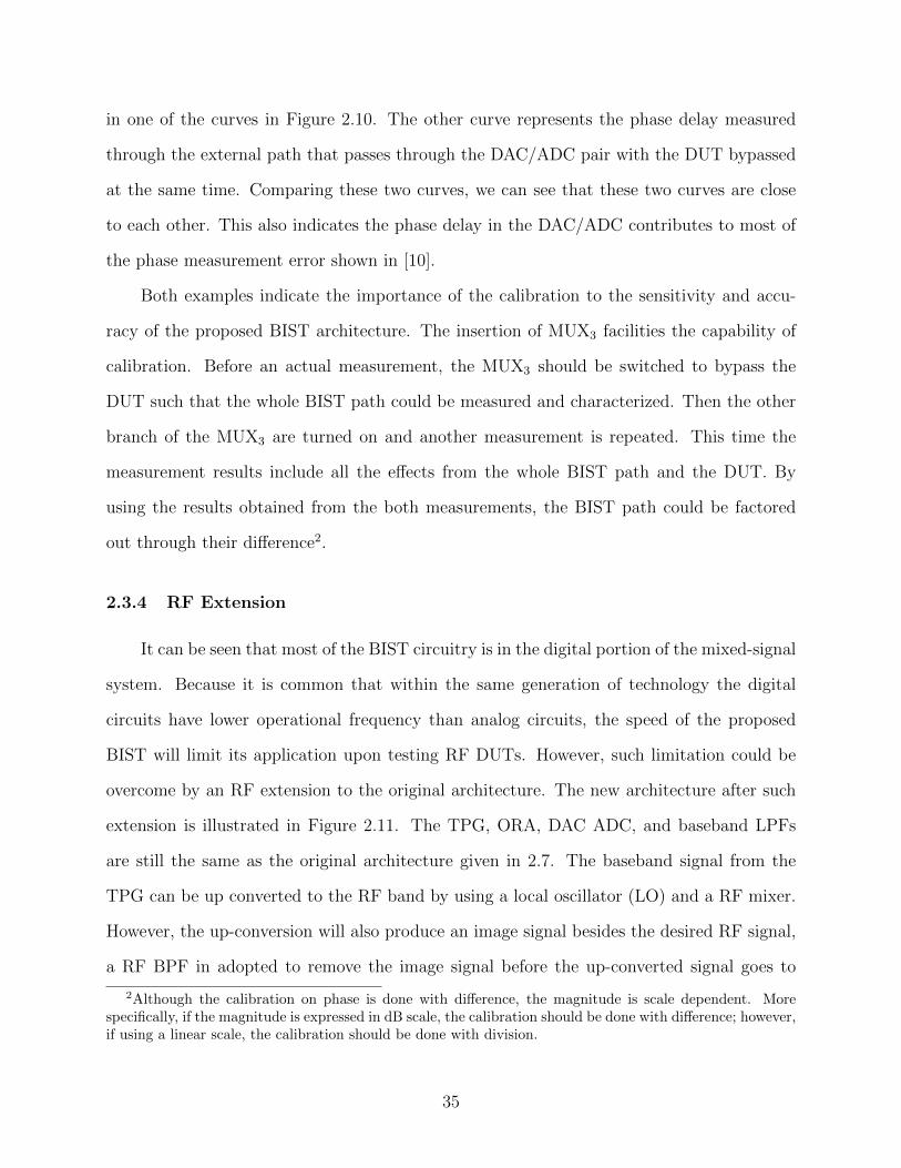
in one of the curves in Figure 2.10. The other curve represents the phase delay measured
through the external path that passes through the DAC/ADC pair with the DUT bypassed
at the same time. Comparing these two curves, we can see that these two curves are close
to each other. This also indicates the phase delay in the DAC/ADC contributes to most of
the phase measurement error shown in [10].
Both examples indicate the importance of the calibration to the sensitivity and accu-
racy of the proposed BIST architecture. The insertion of MUX3 facilities the capability of
calibration. Before an actual measurement, the MUX3 should be switched to bypass the
DUT such that the whole BIST path could be measured and characterized. Then the other
branch of the MUX3 are turned on and another measurement is repeated. This time the
measurement results include all the effects from the whole BIST path and the DUT. By
using the results obtained from the both measurements, the BIST path could be factored
out through their difference2.
2.3.4 RF Extension
It can be seen that most of the BIST circuitry is in the digital portion of the mixed-signal
system. Because it is common that within the same generation of technology the digital
circuits have lower operational frequency than analog circuits, the speed of the proposed
BIST will limit its application upon testing RF DUTs. However, such limitation could be
overcome by an RF extension to the original architecture. The new architecture after such
extension is illustrated in Figure 2.11. The TPG, ORA, DAC ADC, and baseband LPFs
are still the same as the original architecture given in 2.7. The baseband signal from the
TPG can be up converted to the RF band by using a local oscillator (LO) and a RF mixer.
However, the up-conversion will also produce an image signal besides the desired RF signal,
a RF BPF in adopted to remove the image signal before the up-converted signal goes to
2Although the calibration on phase is done with difference, the magnitude is scale dependent. Morespecifically, if the magnitude is expressed in dB scale, the calibration should be done with difference; however,if using a linear scale, the calibration should be done with division.
35
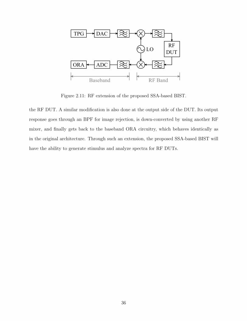
TPG DAC
ORA ADC
RFDUT
Baseband RF Band
LO
Figure 2.11: RF extension of the proposed SSA-based BIST.
the RF DUT. A similar modification is also done at the output side of the DUT. Its output
response goes through an BPF for image rejection, is down-converted by using another RF
mixer, and finally gets back to the baseband ORA circuitry, which behaves identically as
in the original architecture. Through such an extension, the proposed SSA-based BIST will
have the ability to generate stimulus and analyze spectra for RF DUTs.
36
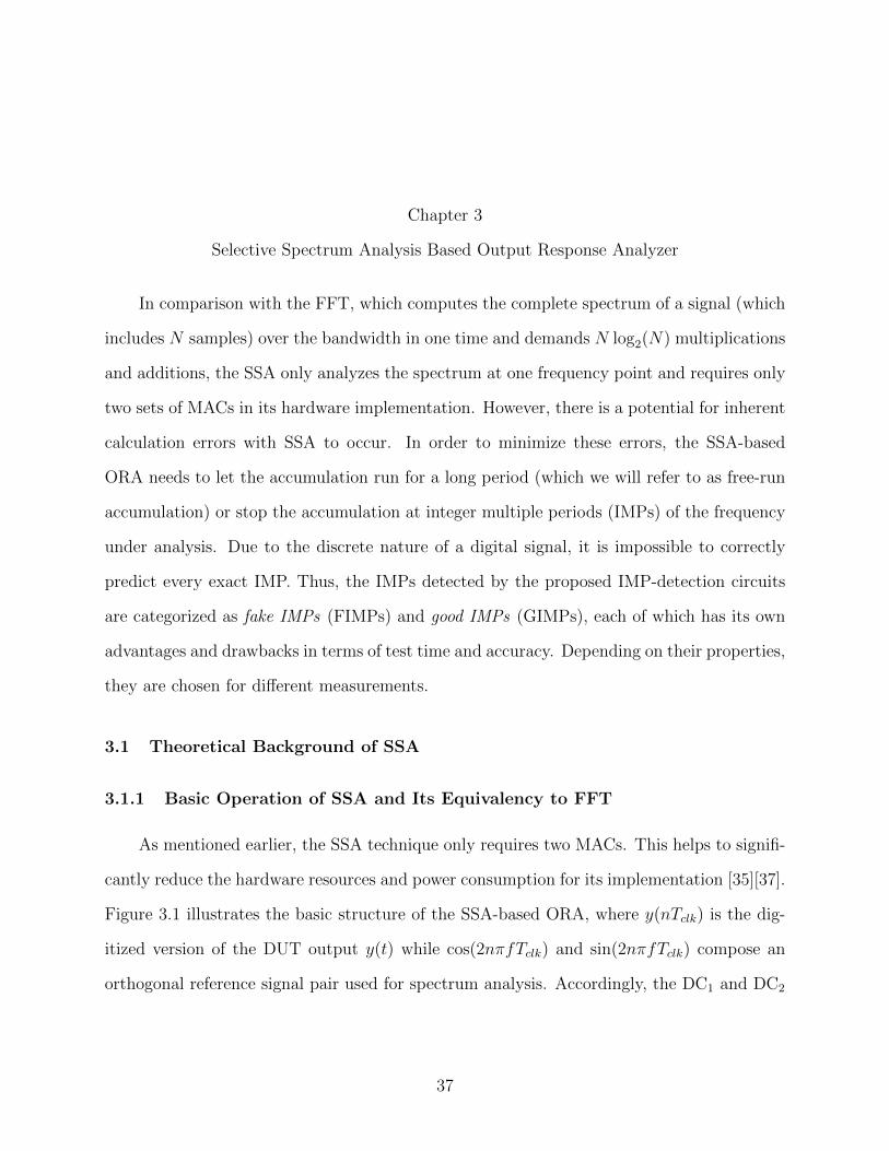
Chapter 3
Selective Spectrum Analysis Based Output Response Analyzer
In comparison with the FFT, which computes the complete spectrum of a signal (which
includes N samples) over the bandwidth in one time and demands N log2(N) multiplications
and additions, the SSA only analyzes the spectrum at one frequency point and requires only
two sets of MACs in its hardware implementation. However, there is a potential for inherent
calculation errors with SSA to occur. In order to minimize these errors, the SSA-based
ORA needs to let the accumulation run for a long period (which we will refer to as free-run
accumulation) or stop the accumulation at integer multiple periods (IMPs) of the frequency
under analysis. Due to the discrete nature of a digital signal, it is impossible to correctly
predict every exact IMP. Thus, the IMPs detected by the proposed IMP-detection circuits
are categorized as fake IMPs (FIMPs) and good IMPs (GIMPs), each of which has its own
advantages and drawbacks in terms of test time and accuracy. Depending on their properties,
they are chosen for different measurements.
3.1 Theoretical Background of SSA
3.1.1 Basic Operation of SSA and Its Equivalency to FFT
As mentioned earlier, the SSA technique only requires two MACs. This helps to signifi-
cantly reduce the hardware resources and power consumption for its implementation [35][37].
Figure 3.1 illustrates the basic structure of the SSA-based ORA, where y(nTclk) is the dig-
itized version of the DUT output y(t) while cos(2nπfTclk) and sin(2nπfTclk) compose an
orthogonal reference signal pair used for spectrum analysis. Accordingly, the DC1 and DC2
37
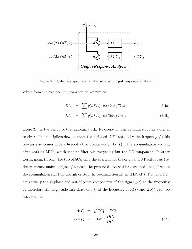
Output Response Analyzer
Figure 3.1: Selective spectrum analysis-based output response analyzer.
values from the two accumulators can be written as
DC1 =∑n
y(nTclk) · cos(2nπfTclk), (3.1a)
DC2 =∑n
y(nTclk) · sin(2nπfTclk), (3.1b)
where Tclk is the period of the sampling clock. Its operation can be understood as a digital
receiver. The multipliers down-convert the digitized DUT output by the frequency f (this
process also comes with a byproduct of up-conversion by f). The accumulations coming
after work as LPFs, which tend to filter out everything but the DC component. In other
words, going through the two MACs, only the spectrum of the original DUT output y(t) at
the frequency under analysis f tends to be preserved. As will be discussed later, if we let
the accumulation run long enough or stop the accumulation at the IMPs of f , DC1 and DC2
are actually the in-phase and out-of-phase components of the signal y(t) at the frequency
f . Therefore the magnitude and phase of y(t) at the frequency f , A(f) and ∆φ(f), can be
calculated as
A(f) =√DC2
1 +DC22 ,
∆φ(f) = − tan−1 DC2
DC1
. (3.2)
38
The mathematical expression of the FFT of a digital signal with N samples is given by
Y (k) =N−1∑n=0
y(n)e−j2πkn/N , 0 ≤ k ≤ N − 1
=N−1∑n=0
y(n) cos
(2πkn
N
)− j
N−1∑n=0
y(n) sin
(2πkn
N
), (3.3)
where y(n) is a digitized signal in time domain and Y (k) is its discrete spectrum at frequency
kN· 1Tclk
. Substituting f in Equation (3.1) with kN· 1Tclk
, Equation (3.3) can be rewritten as
Y (k) = DC1(k)− jDC2(k). (3.4)
Thus, the magnitude and phase of the spectrum Y (k) can be calculated by using the exact
equation of (3.2). Therefore, by setting the reference signals cos(2nπfTclk) and sin(2nπfTclk)
at different frequencies of kNfclk, the SSA-based ORA performs identical spectrum analysis
as FFT. However, since the SSA has more freedom to pick frequency f , instead of just
kNfclk, 0 ≤ k ≤ N − 1, it is actually an FFT with k equal to any arbitrary rational number.
Yet this does not mean that SSA is able to achieve a higher frequency resolution than FFT.
3.1.2 Frequency Resolution of SSA
One interesting property hidden in Equation (3.3) is that given a signal sequence y(n)
with N samples only the spectrum at kNfclk, 0 ≤ k ≤ N − 1 can be accurately estimated
regardless whether using SSA or FFT. In other words, the frequency resolution of spectrum
analysis is determined by 1Nfclk. This means that even though Y (k), when k is equal to a
fractional number, can be calculated, the results are not exactly as expected. Figure 3.2
demonstrates such an example. The signal under analysis is a 2-period sinusoidal wave in
the top plot. The spectra calculated at 1Nfclk are plotted as the solid circle in the bottom
plot, where the spectrum contents only appear at its own frequency as supposed. However,
if the spectrum analysis is done with finer frequency spacing, the spectrum becomes the
39
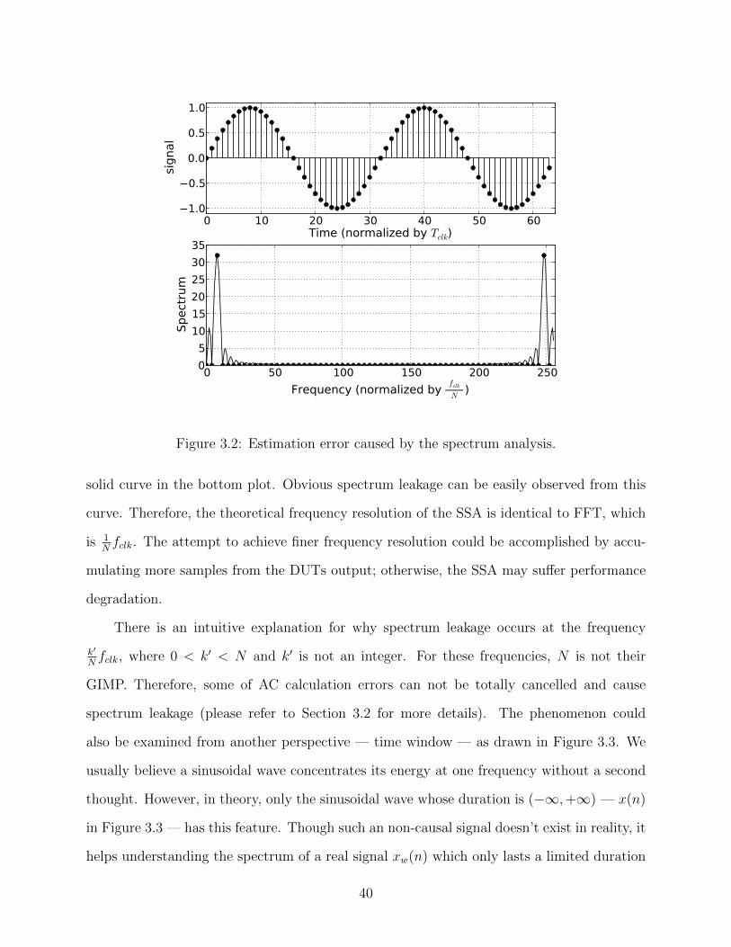
0 10 20 30 40 50 60Time (normalized by Tclk)
1.0
0.5
0.0
0.5
1.0
sign
al
0 50 100 150 200 250Frequency (normalized by fclk
N)
05
101520253035
Spec
trum
Figure 3.2: Estimation error caused by the spectrum analysis.
solid curve in the bottom plot. Obvious spectrum leakage can be easily observed from this
curve. Therefore, the theoretical frequency resolution of the SSA is identical to FFT, which
is 1Nfclk. The attempt to achieve finer frequency resolution could be accomplished by accu-
mulating more samples from the DUTs output; otherwise, the SSA may suffer performance
degradation.
There is an intuitive explanation for why spectrum leakage occurs at the frequency
k′
Nfclk, where 0 < k′ < N and k′ is not an integer. For these frequencies, N is not their
GIMP. Therefore, some of AC calculation errors can not be totally cancelled and cause
spectrum leakage (please refer to Section 3.2 for more details). The phenomenon could
also be examined from another perspective — time window — as drawn in Figure 3.3. We
usually believe a sinusoidal wave concentrates its energy at one frequency without a second
thought. However, in theory, only the sinusoidal wave whose duration is (−∞,+∞) — x(n)
in Figure 3.3 — has this feature. Though such an non-causal signal doesn’t exist in reality, it
helps understanding the spectrum of a real signal xw(n) which only lasts a limited duration
40
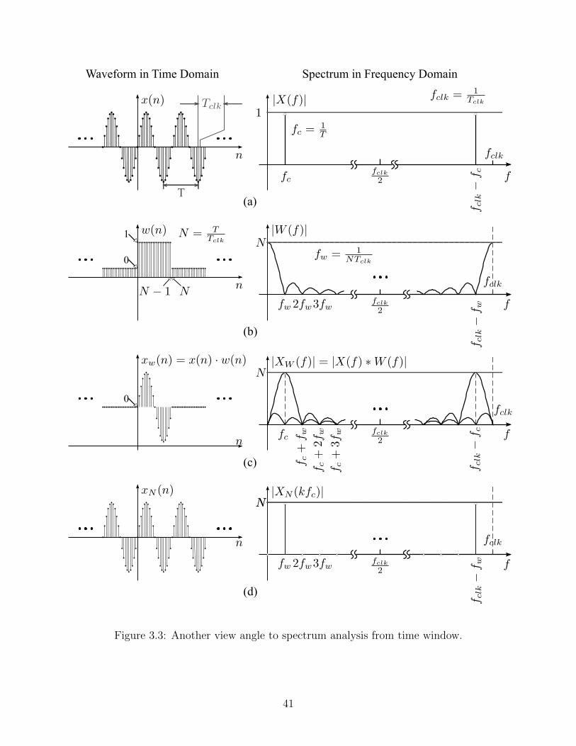
Waveform in Time Domain Spectrum in Frequency Domain
T
0
1
0
(a)
(d)
(c)
(b)
Figure 3.3: Another view angle to spectrum analysis from time window.
41

because xw(n) can be treated as a shortened version of x(n) on time by a rectangle window
w(n), which is expressed as
w(n) =
1 , t = 0, 1, 2, · · · , (N − 1),
0 , otherwise.(3.5)
The spectrum of the rectangle window w(n) can be obtained through a simple derivation as
followed,
W (f) =N−1∑n=0
w(n)e−j2πfnTclk =N−1∑n=0
e−j2πfnTclk =1− ej2πfNTclk1− e−2πfTclk
= ejπf(N−1)nTclksin(NπfTclk)
sin(πfTclk). (3.6)
Its magnitude |W (f)| is a digital sinc function1 expressed as
|W (f)| = sin(NπfTclk)
sin(πfTclk)(3.7)
and is drawn in Figure 3.3-(b). From the figure, two interesting characteristics can be
observed:
• |W (f)| is equal to 0 at the frequency of fw = 1NTclk
and its harmonics, so its main lobe
is narrowed as the time duration of the window, N , increases;
• |W (0)| is equal to N , so the main lobe grows taller as N increases;
In fact, the window operation is a multiplication on the time domain; in other words,
xw(n) = x(n) · w(n). (3.8)
According to convolution theorem, if a digital signal is the product of two other signals, its
spectrum is equal to the cyclic convolution of the latter two signals’ spectrum. Therefore,
1the digital sinc function has very similar shape as the usual sinc function sin(x)x .
42
XW (f) = X(f) ∗W (f), where ∗ is the cyclic convolution operator. Or else, we can calculate
the spectrum of xw(n) directly from the definition of the Fourier’s Transform:
XW (f) =+∞∑
n=−∞
xw(n)ej2πfnTclk =N−1∑n=0
xw(n)ej2πfnTclk =N−1∑n=0
x(n)ej2πfnTclk . (3.9)
If we sample the xw(n)’s spectrum, XW (f), at the frequency of kNfclk = kfw, k = 0, 1, . . . , N−
1, the spectrum at these frequency points can be expressed as
XW (k
Nfclk) =
N−1∑n=0
xw(n)ej2πnkN , (3.10)
which is exactly same as the FFT’s definition in Equation (3.3). This derivation shows that
the FFT, in essence, shortens the signal under analysis by a rectangle window on the time
before analyzing its spectrum. At the same time, the sampling happened in the frequency
domain makes the shortened signal repeat itself in the time domain as demonstrated in the
bottom plot of Figure 3.3. It should be noted that in Figure 3.3 the time duration of the
window function w(n) is exactly the period of the signal, fw = 1NTclk
= 1T
= fc. So even
though the cyclic convolution makes the shape of the spectrum deviate from the digital sinc
function as illustrated in Figure 3.3-(c), the frequency sampling happened at kfw still gets
the perfect results as desired.
It is clear that as the accumulation length N increases, the main lobe of |W (f)| becomes
narrower and taller and thus less spectrum leakage. Suppose the input signal is a one-tone
signal at frequency fc and accumulation length N is used for the SSA, the main lobe will be
at the frequency range of [fc − fclkN, fc + fclk
N]. In order to detect this tone, the analysis tone
has to hit the main lobe. Therefore, the spectrum has to be scanned through a minimum
set of frequencies, { kNfclk, k = 0, 1, 2, · · · , dN
2e − 1}. Therefore, given an accumulation N ,
the NCO3 has to at least offer a frequency resolution fclkN
. Therefore,
fclk2Mfull
≤ fclkN
=⇒ Mfull ≥ dlog2Ne. (3.11)
43
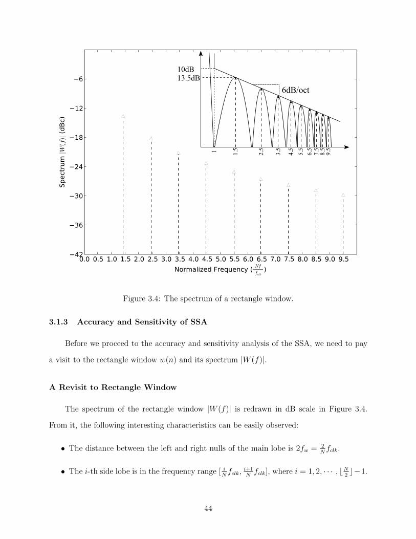
6dB/oct
13.5dB10dB
1 1.5
2.5
3.5
4.5
5.5
6.57.58.59.5
Figure 3.4: The spectrum of a rectangle window.
3.1.3 Accuracy and Sensitivity of SSA
Before we proceed to the accuracy and sensitivity analysis of the SSA, we need to pay
a visit to the rectangle window w(n) and its spectrum |W (f)|.
A Revisit to Rectangle Window
The spectrum of the rectangle window |W (f)| is redrawn in dB scale in Figure 3.4.
From it, the following interesting characteristics can be easily observed:
• The distance between the left and right nulls of the main lobe is 2fw = 2Nfclk.
• The i-th side lobe is in the frequency range [ iNfclk,
i+1Nfclk], where i = 1, 2, · · · , bN
2c−1.
44
• The peak value of the i-th side lobe roughly happens at the frequency of 2i+12N
fclk, where
the numerator of Equation (3.7), sin(NπfTclk), is equal to 1. Therefore, the maximum
value of the i-th side lobe is around
|W (f)|max, i-th lobe =1
sin(2i+12N
π)≈ N
(i+ 0.5)π. (3.12)
The approximation holds true when
i ≤ 0.175N − 0.5 =⇒ i ≤ 0.175N if N ≥ 29. (3.13)
According to Equation (3.12), the peak of the side lobe attenuates inversely propor-
tional to the lobe index i. However, after i goes beyond Equation (3.13), the attenua-
tion rate of the side lobe becomes slower.
• The peak value of the last lobe right before fclk2
occurs at the frequency around
bN2c−0.5
Nfclk and the peak value is around 1.
The peak of the side lobe is redrawn in the mini-plot in Figure 3.4 where the normalized
frequency is drawn on the log scale. An obvious 6dB/Octave attenuation curve is observed
when the condition in Equation (3.13) is satisfied. Given a frequency offset ∆f , the index
of the side lobe to which ∆f belongs, i, can be calculated as
i =
⌊N∆f
fclk
⌋. (3.14)
Substituting i in Equation (3.13) with Equation (3.14), we can get that when
fclkN≤ ∆f ≤ 0.175fclk, (3.15)
45
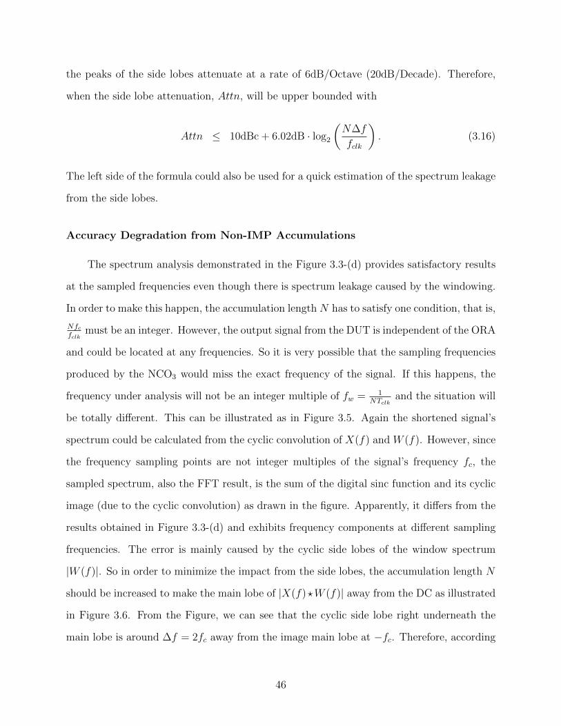
the peaks of the side lobes attenuate at a rate of 6dB/Octave (20dB/Decade). Therefore,
when the side lobe attenuation, Attn, will be upper bounded with
Attn ≤ 10dBc + 6.02dB · log2
(N∆f
fclk
). (3.16)
The left side of the formula could also be used for a quick estimation of the spectrum leakage
from the side lobes.
Accuracy Degradation from Non-IMP Accumulations
The spectrum analysis demonstrated in the Figure 3.3-(d) provides satisfactory results
at the sampled frequencies even though there is spectrum leakage caused by the windowing.
In order to make this happen, the accumulation length N has to satisfy one condition, that is,
Nfcfclk
must be an integer. However, the output signal from the DUT is independent of the ORA
and could be located at any frequencies. So it is very possible that the sampling frequencies
produced by the NCO3 would miss the exact frequency of the signal. If this happens, the
frequency under analysis will not be an integer multiple of fw = 1NTclk
and the situation will
be totally different. This can be illustrated as in Figure 3.5. Again the shortened signal’s
spectrum could be calculated from the cyclic convolution of X(f) and W (f). However, since
the frequency sampling points are not integer multiples of the signal’s frequency fc, the
sampled spectrum, also the FFT result, is the sum of the digital sinc function and its cyclic
image (due to the cyclic convolution) as drawn in the figure. Apparently, it differs from the
results obtained in Figure 3.3-(d) and exhibits frequency components at different sampling
frequencies. The error is mainly caused by the cyclic side lobes of the window spectrum
|W (f)|. So in order to minimize the impact from the side lobes, the accumulation length N
should be increased to make the main lobe of |X(f)?W (f)| away from the DC as illustrated
in Figure 3.6. From the Figure, we can see that the cyclic side lobe right underneath the
main lobe is around ∆f = 2fc away from the image main lobe at −fc. Therefore, according
46
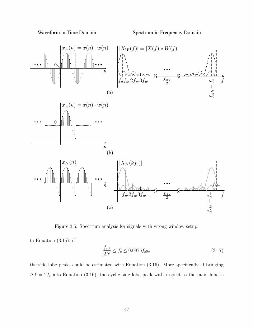
Waveform in Time Domain Spectrum in Frequency Domain
0
0
(a)
(b)
(c)
Figure 3.5: Spectrum analysis for signals with wrong window setup.
to Equation (3.15), if
fclk2N≤ fc ≤ 0.0875fclk, (3.17)
the side lobe peaks could be estimated with Equation (3.16). More specifically, if bringing
∆f = 2fc into Equation (3.16), the cyclic side lobe peak with respect to the main lobe is
47
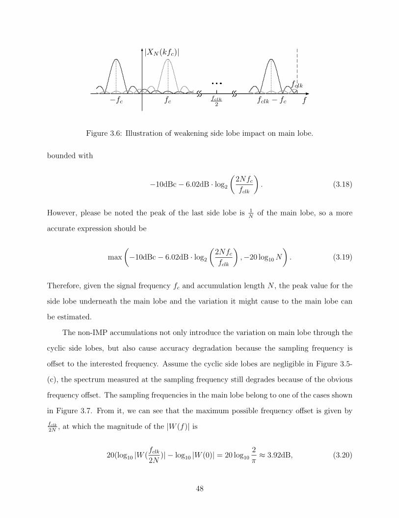
Figure 3.6: Illustration of weakening side lobe impact on main lobe.
bounded with
−10dBc− 6.02dB · log2
(2Nfcfclk
). (3.18)
However, please be noted the peak of the last side lobe is 1N
of the main lobe, so a more
accurate expression should be
max
(−10dBc− 6.02dB · log2
(2Nfcfclk
),−20 log10N
). (3.19)
Therefore, given the signal frequency fc and accumulation length N , the peak value for the
side lobe underneath the main lobe and the variation it might cause to the main lobe can
be estimated.
The non-IMP accumulations not only introduce the variation on main lobe through the
cyclic side lobes, but also cause accuracy degradation because the sampling frequency is
offset to the interested frequency. Assume the cyclic side lobes are negligible in Figure 3.5-
(c), the spectrum measured at the sampling frequency still degrades because of the obvious
frequency offset. The sampling frequencies in the main lobe belong to one of the cases shown
in Figure 3.7. From it, we can see that the maximum possible frequency offset is given by
fclk2N
, at which the magnitude of the |W (f)| is
20(log10 |W (fclk2N
)| − log10 |W (0)| = 20 log10
2
π≈ 3.92dB, (3.20)
48
Case #1: Case #2: Case #3:
Figure 3.7: Illustration of accuracy degradation by sampling frequency offset.
according to Equation (3.7). Therefore, the maximum measurement error from the sampling
frequency offset is up to 3.92dB.
Signal vs. Noise Floor
As mentioned in Section 2.2.1, it is inevitable that the DUT’s output, y(iTclk), will be
contaminated by different kinds of noise. Two widely accepted and used assumptions for
noise are given as
E[n(iTclk)] = 0, (3.21a)
E[n(iTclk) · n(kTclk)] =
n20, if i=k,
0, otherwise,(3.21b)
where n(iTclk) is the noise in the sampled signal, n20 is the total noise power, and E[·] is the
expected value of a random variable. As a stochastic process, the n(iTclk)’s power spectrum
density (PSD) can be estimated from
PSD = E[|N(f)|2] = E
[N−1∑i=0
n(iTclk)e−j2πfiTclk ·
N−1∑k=0
n(kTclk)ej2πfkTclk
]
=N−1∑i=0
N−1∑k=0
E[n(iTclk) · n(kTclk)] · ej2πf(k−i)Tclk =N−1∑i=0
n20 = N · n2
0, (3.22)
49
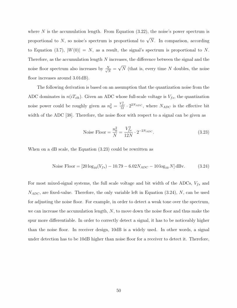
where N is the accumulation length. From Equation (3.22), the noise’s power spectrum is
proportional to N , so noise’s spectrum is proportional to√N . In comparison, according
to Equation (3.7), |W (0)| = N , as a result, the signal’s spectrum is proportional to N .
Therefore, as the accumulation length N increases, the difference between the signal and the
noise floor spectrum also increases by N√N
=√N (that is, every time N doubles, the noise
floor increases around 3.01dB).
The following derivation is based on an assumption that the quantization noise from the
ADC dominates in n(iTclk). Given an ADC whose full-scale voltage is Vfs, the quantization
noise power could be roughly given as n20 =
V 2fs
12· 22NADC , where NADC is the effective bit
width of the ADC [38]. Therefore, the noise floor with respect to a signal can be given as
Noise Floor =n2
0
N=
V 2fs
12N· 2−2NADC . (3.23)
When on a dB scale, the Equation (3.23) could be rewritten as
Noise Floor = [20 log10(Vfs)− 10.79− 6.02NADC − 10 log10N ] dBv. (3.24)
For most mixed-signal systems, the full scale voltage and bit width of the ADCs, Vfs and
NADC , are fixed-value. Therefore, the only variable left in Equation (3.24), N , can be used
for adjusting the noise floor. For example, in order to detect a weak tone over the spectrum,
we can increase the accumulation length, N , to move down the noise floor and thus make the
spur more differentiable. In order to correctly detect a signal, it has to be noticeably higher
than the noise floor. In receiver design, 10dB is a widely used. In other words, a signal
under detection has to be 10dB higher than noise floor for a receiver to detect it. Therefore,
50
given a tone of SdBv, the noise floor should satisfy
Noise Floor = [20 log10(Vfs)− 10.79− 6.02NADC − 10 log10N ] dBv ≤ [S − 10]dBv
⇓
N ≥ 1020 log10(Vfs)−0.79−6.02NADC−S
10 . (3.25)
According to Equation (3.25), for a mixed-signal system utilizing a 12-bit, 1Vpp ADC, the
accumulation length N has to satisfy
N ≥ 10−S−73.03
10 (3.26)
to detect a tone of SdBv.
Desensitization in SSA
The previous discussion is based on an assumption there is only one strong frequency
component over the spectrum. However, the situation could be more complicated if the
signal appears at several frequencies. Figure 3.8 demonstrates a case when the signal has
two frequency components with similar strength. The left plots shows if the window duration
N is small (in SSA, N refers to the length of accumulation), the power leakage from the
window function could mix two components together and make them undifferentiated. Under
such situation, we need to increase the window duration N (or accumulation length in SSA),
which will narrow down the width of the main lobe of w(n)’s spectrum, W (f). By doing
this, the spectrum at these two frequencies will become more differentiable as shown in the
right plot of Figure 3.8.
Another case is that there are two frequency components while the interested one is
much weaker than the other one. This could be illustrated as in Figure 3.9. From it, we can
clearly see that it is possible that the side lobes of the strong frequency component at fc1
could submerge the interested yet weak one at fc2. In order to make the weak component
51
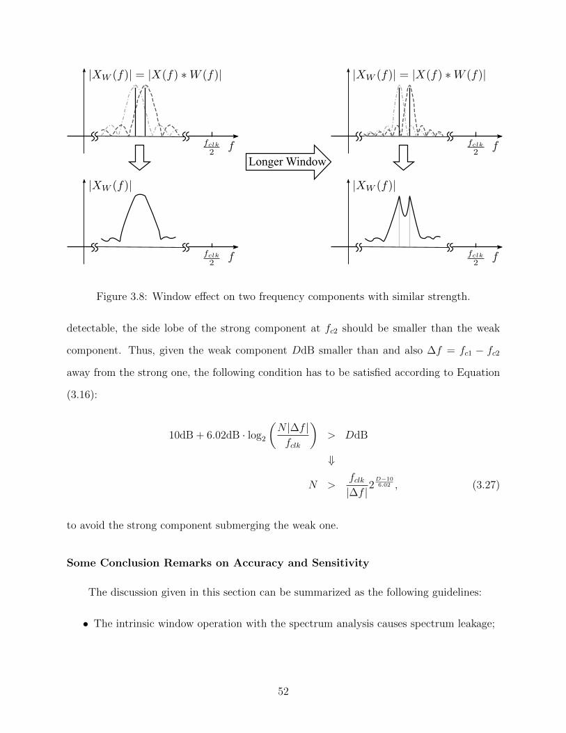
Longer Window
Figure 3.8: Window effect on two frequency components with similar strength.
detectable, the side lobe of the strong component at fc2 should be smaller than the weak
component. Thus, given the weak component DdB smaller than and also ∆f = fc1 − fc2
away from the strong one, the following condition has to be satisfied according to Equation
(3.16):
10dB + 6.02dB · log2
(N |∆f |fclk
)> DdB
⇓
N >fclk|∆f |
2D−106.02 , (3.27)
to avoid the strong component submerging the weak one.
Some Conclusion Remarks on Accuracy and Sensitivity
The discussion given in this section can be summarized as the following guidelines:
• The intrinsic window operation with the spectrum analysis causes spectrum leakage;
52
Spectrum
Figure 3.9: Desensitization in spectrum analysis.
• The frequency resolution of the spectrum analysis is determined by the accumulation
length N and given by fclkN
;
• The frequency resolution of the NCO3 in SSA is determined by the bit width of the
phase accumulator Mfull and given by fclk2Mfull
;
• For spectrum sweeping, the frequency resolution of the NCO3 in SSA has to be finer
than the resolution of the spectrum analysis. Thus, Mfull ≥ dlog2Ne;
• The non-IMP accumulation introduces variation from the cyclic side lobes. Increasing
accumulation length N helps to mitigate the side lobe effect as given in Equation
(3.19);
• The non-IMP accumulation also produces the sampling frequency offset and the caused
error is bounded by around 3.92dB;
• The noise floor with respect to the signal measured by spectrum analysis technique
decreases by√N times (or 10 log10NdB in dB scale) as the accumulation length N
increases;
• The spectrum leakage of the spectrum analysis could cause desensitization of a weak
frequency components if another strong one presents. Again increasing accumulation
length N helps to solve the issue and the determination of N is given by Equation
(3.27).
53
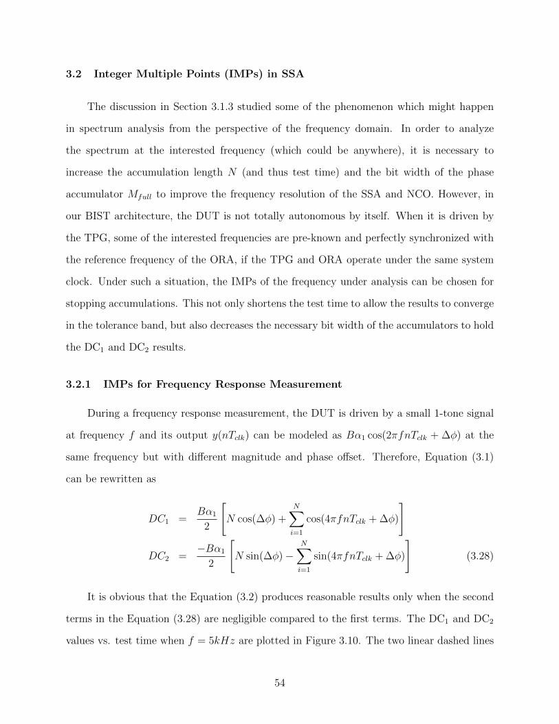
3.2 Integer Multiple Points (IMPs) in SSA
The discussion in Section 3.1.3 studied some of the phenomenon which might happen
in spectrum analysis from the perspective of the frequency domain. In order to analyze
the spectrum at the interested frequency (which could be anywhere), it is necessary to
increase the accumulation length N (and thus test time) and the bit width of the phase
accumulator Mfull to improve the frequency resolution of the SSA and NCO. However, in
our BIST architecture, the DUT is not totally autonomous by itself. When it is driven by
the TPG, some of the interested frequencies are pre-known and perfectly synchronized with
the reference frequency of the ORA, if the TPG and ORA operate under the same system
clock. Under such a situation, the IMPs of the frequency under analysis can be chosen for
stopping accumulations. This not only shortens the test time to allow the results to converge
in the tolerance band, but also decreases the necessary bit width of the accumulators to hold
the DC1 and DC2 results.
3.2.1 IMPs for Frequency Response Measurement
During a frequency response measurement, the DUT is driven by a small 1-tone signal
at frequency f and its output y(nTclk) can be modeled as Bα1 cos(2πfnTclk + ∆φ) at the
same frequency but with different magnitude and phase offset. Therefore, Equation (3.1)
can be rewritten as
DC1 =Bα1
2
[N cos(∆φ) +
N∑i=1
cos(4πfnTclk + ∆φ)
]
DC2 =−Bα1
2
[N sin(∆φ)−
N∑i=1
sin(4πfnTclk + ∆φ)
](3.28)
It is obvious that the Equation (3.2) produces reasonable results only when the second
terms in the Equation (3.28) are negligible compared to the first terms. The DC1 and DC2
values vs. test time when f = 5kHz are plotted in Figure 3.10. The two linear dashed lines
54
Figure 3.10: DC1 and DC2 vs. test time in frequency response measurement.
represent the first terms in the DC1 and DC2 expressions of (3.28), and the AC periodic
components riding on the dashed lines represent calculation errors introduced by the second
terms. Since these AC components are bounded, they become negligible if the accumulations
are performed for a sufficient length of time, which we call “free-run accumulation”. However,
the calculation errors go to zero at a period of 12f
. The period read from the figure is around
0.1ms = 1/(2 × 5kHz). Therefore, as long as the accumulation can be stopped at the half
IMPs of f , calculation errors are minimized, if not eliminated.
3.2.2 Linearity Measurement
The P1dB measurement uses 1-tone stimulus with the information of interest located
at the fundamental frequency, so that it can be analyzed in a similar way as a frequency
response measurement. However, the IP3 measurement is different because the strongest
DUT’s output spectrum appears at four frequencies, as illustrated in Figure 2.5. Since
55

the frequencies are spaced very closely, it is feasible to assume that the spectrum at these
frequencies experiences the approximately same phase delay. Therefore, the DUT’s output
y(nTclk) in the IP3 measurement can be modeled as
f(nTclk) = A0 cos[(2ω1 − ω2)nTclk + θ] + A1 cos(ω1nTclk + θ) +
A1 cos(ω2nTclk + θ) + A0 cos[(2ω2 − ω1)nTclk + θ], (3.29)
∆P = 20 log10A1 − 20 log10A2, (3.30)
∆ω = ω2 − ω1 = 2π(f2 − f1) = ∆f. (3.31)
In an IP3 measurement, the ORA needs to perform two SSAs to obtain y(nTclk)’s
spectrum at either LSB or USB. As an example, the DC1 and DC2 values obtained at LSB
can be derived as
DC1(f1) =A1N
2cos θ +
1
2
N∑n=1
[(A1 + A0) cos(∆ωnTclk + θ) + A0 cos(2∆ωnTclk + θ) +
A0 cos((2ω1 −∆ω)nTclk + θ)] +
1
2
N∑n=1
[A1 cos(2ω1nTclk + θ) + A1 cos((2ω1 + ∆ω)nTclk + θ) +
A0 cos((2ω1 + 2∆ω)nTclk + θ)], (3.32)
DC2(f1) = −A1N
2sin θ −
1
2
N∑n=1
[(A1 − A0) sin(∆ωnTclk + θ) + A0 sin(2∆ωnTclk + θ)−
A0 sin((2ω1 −∆ω)nTclk + θ)] +
1
2
N∑n=1
[A1 sin(2ω1nTclk + θ) + A1 sin((2ω1 + ∆ω)nTclk + θ) +
A0 sin((2ω1 + 2∆ω)nTclk + θ)], (3.33)
56
DC1(2f1 − f2) =A0N
2cos θ +
1
2
N∑n=1
[A1 cos(∆ωnTclk + θ) + A1 cos(2∆ωnTclk + θ) +
A0 cos(3∆ωnTclk + θ)] +
1
2
N∑n=1
[A0 cos(2(ω1 −∆ω)nTclk + θ) + A1 cos((2ω1 −∆ω)nTclk + θ)] +
1
2
N∑n=1
[A1 cos(2ω1nTclk + θ) + A0 cos((2ω1 + ∆ω)nTclk + θ)], (3.34)
DC2(2f1 − f2) = −A0N
2sin θ −
1
2
N∑n=1
[A1 sin(∆ωnTclk + θ) + A1 sin(2∆ωnTclk + θ) +
A0 sin(3∆ωnTclk + θ)] +
1
2
N∑n=1
[A0 sin(2(ω1 −∆ω)nTclk + θ) + A1 sin((2ω1 −∆ω)nTclk + θ)] +
1
2
N∑n=1
[A1 sin(2ω1nTclk + θ) + A0 sin((2ω1 + ∆ω)nTclk + θ)]. (3.35)
Similar to the frequency response measurement, the first terms in these equations are
the desired DC values and the calculation error need be minimized. While this goal can be
achieved by using free-run accumulation, the required test time can be prohibitively high,
as will be shown in Section 3.3.3. From Eqaution (3.32) to Equation (3.35), the periods of
the error terms, ferr, can be
ferr =
n∆f n=1,2,3
2f1 + n∆f n=-2,-1,0,1,2(3.36)
Therefore, if the ORA can stop accumulation at the common IMPs (CIMPs) of all
possible ferr, the calculation errors can be minimized. Interestingly, the CIMPs of LSB
frequencies are also CIMPs of all ferr. This property can be proven as follows.
57
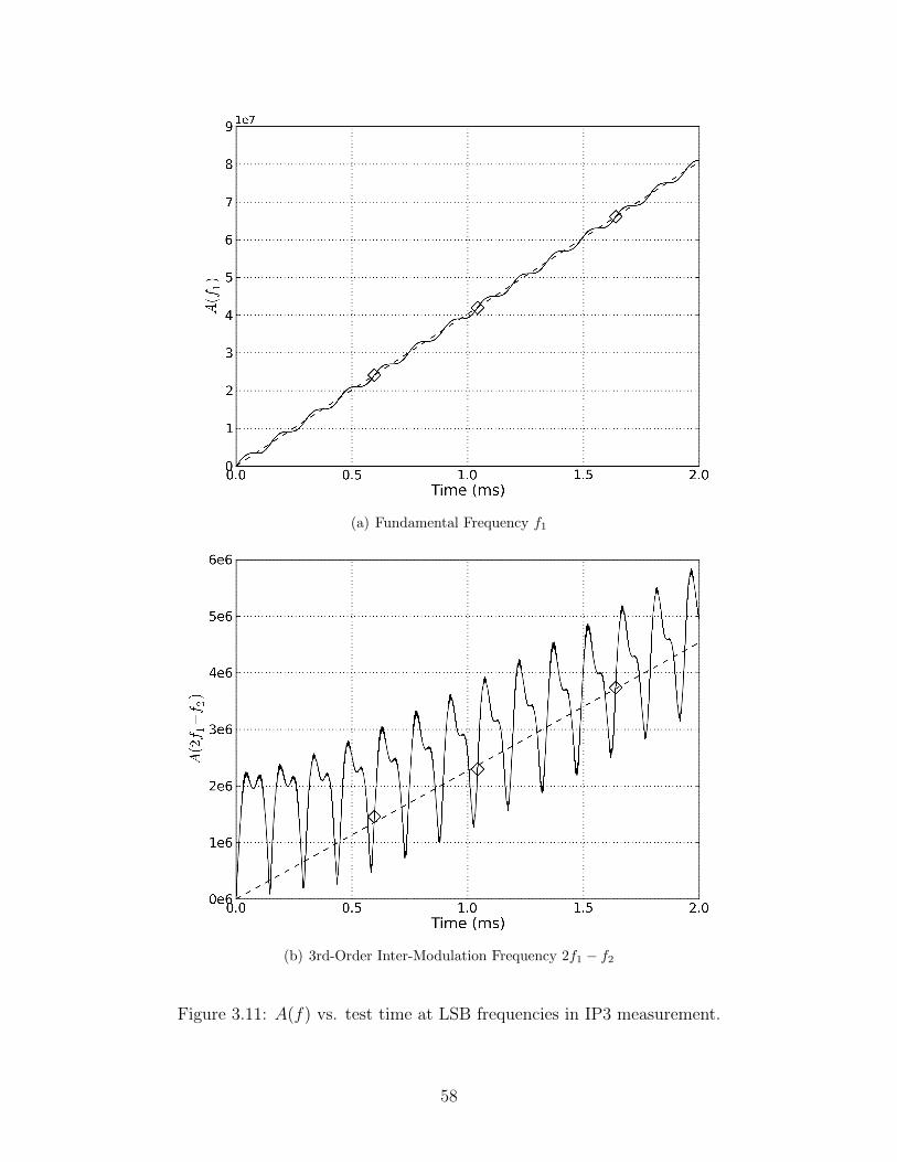
(a) Fundamental Frequency f1
(b) 3rd-Order Inter-Modulation Frequency 2f1 − f2
Figure 3.11: A(f) vs. test time at LSB frequencies in IP3 measurement.
58
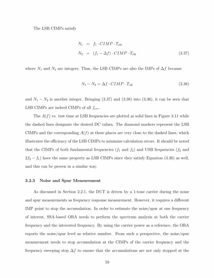
The LSB CIMPs satisfy
N1 = f1 · CIMP · Tclk
N2 = (f1 −∆f) · CIMP · Tclk (3.37)
where N1 and N2 are integers. Thus, the LSB CIMPs are also the IMPs of ∆f because
N1 −N2 = ∆f · CIMP · Tclk (3.38)
and N1 − N2 is another integer. Bringing (3.37) and (3.38) into (3.36), it can be seen that
LSB CIMPs are indeed CIMPs of all ferr.
The A(f) vs. test time at LSB frequencies are plotted as solid lines in Figure 3.11 while
the dashed lines designate the desired DC values. The diamond markers represent the LSB
CIMPs and the corresponding A(f) at these places are very close to the dashed lines, which
illustrates the efficiency of the LSB CIMPs to minimize calculation errors. It should be noted
that the CIMPs of both fundamental frequencies (f1 and f2) and USB frequencies (f2 and
2f2 − f1) have the same property as LSB CIMPs since they satisfy Equation (3.36) as well,
and this can be proven in a similar way.
3.2.3 Noise and Spur Measurement
As discussed in Section 2.2.1, the DUT is driven by a 1-tone carrier during the noise
and spur measurements as frequency response measurement. However, it requires a different
IMP point to stop the accumulation. In order to estimate the noise/spur at one frequency
of interest, SSA-based ORA needs to perform the spectrum analysis at both the carrier
frequency and the interested frequency. By using the carrier power as a reference, the ORA
reports the noise/spur level as relative number. From such a perspective, the noise/spur
measurement needs to stop accumulation at the CIMPs of the carrier frequency and the
frequency sweeping step ∆f to ensure that the accumulations are not only stopped at the
59
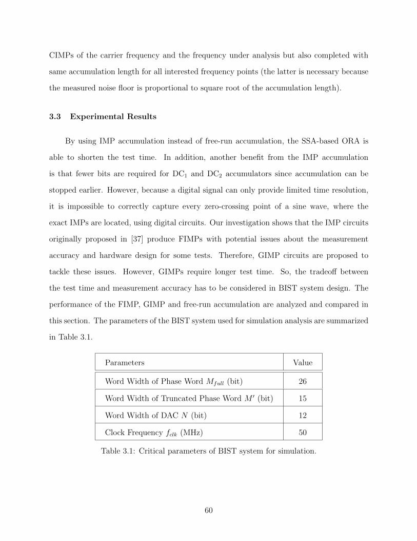
CIMPs of the carrier frequency and the frequency under analysis but also completed with
same accumulation length for all interested frequency points (the latter is necessary because
the measured noise floor is proportional to square root of the accumulation length).
3.3 Experimental Results
By using IMP accumulation instead of free-run accumulation, the SSA-based ORA is
able to shorten the test time. In addition, another benefit from the IMP accumulation
is that fewer bits are required for DC1 and DC2 accumulators since accumulation can be
stopped earlier. However, because a digital signal can only provide limited time resolution,
it is impossible to correctly capture every zero-crossing point of a sine wave, where the
exact IMPs are located, using digital circuits. Our investigation shows that the IMP circuits
originally proposed in [37] produce FIMPs with potential issues about the measurement
accuracy and hardware design for some tests. Therefore, GIMP circuits are proposed to
tackle these issues. However, GIMPs require longer test time. So, the tradeoff between
the test time and measurement accuracy has to be considered in BIST system design. The
performance of the FIMP, GIMP and free-run accumulation are analyzed and compared in
this section. The parameters of the BIST system used for simulation analysis are summarized
in Table 3.1.
Parameters Value
Word Width of Phase Word Mfull (bit) 26
Word Width of Truncated Phase Word M ′ (bit) 15
Word Width of DAC N (bit) 12
Clock Frequency fclk (MHz) 50
Table 3.1: Critical parameters of BIST system for simulation.
60
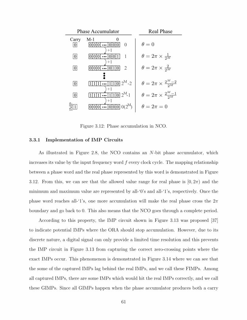
0 0M-1 0Carry
+1
Phase Accumulator Real Phase
IMP
0
M
0 0 0 0 0
+11
2
1 +1
2 -21 1 1 1 0
+12 -1
0(2 )
M
M
0 0 0 0 0 0 1
0 0 0 0 0 1 0
0 1 0 0 0 0 0
0
0 1 1 1 1 1 0
Figure 3.12: Phase accumulation in NCO.
3.3.1 Implementation of IMP Circuits
As illustrated in Figure 2.8, the NCO contains an N -bit phase accumulator, which
increases its value by the input frequency word f every clock cycle. The mapping relationship
between a phase word and the real phase represented by this word is demonstrated in Figure
3.12. From this, we can see that the allowed value range for real phase is [0, 2π) and the
minimum and maximum value are represented by all-‘0’s and all-‘1’s, respectively. Once the
phase word reaches all-‘1’s, one more accumulation will make the real phase cross the 2π
boundary and go back to 0. This also means that the NCO goes through a complete period.
According to this property, the IMP circuit shown in Figure 3.13 was proposed [37]
to indicate potential IMPs where the ORA should stop accumulation. However, due to its
discrete nature, a digital signal can only provide a limited time resolution and this prevents
the IMP circuit in Figure 3.13 from capturing the correct zero-crossing points where the
exact IMPs occur. This phenomenon is demonstrated in Figure 3.14 where we can see that
the some of the captured IMPs lag behind the real IMPs, and we call these FIMPs. Among
all captured IMPs, there are some IMPs which would hit the real IMPs correctly, and we call
these GIMPs. Since all GIMPs happen when the phase accumulator produces both a carry
61

carry out
clk
f
FIMP
Phase Word
Phase Accumulator
D QMfull
MfullMfull MfullMfull
Figure 3.13: FIMP detector.
out flag and an all-‘0’s phase word, a GIMP detector could be realized by using a simple
circuit shown in Figure 3.15.
If the accumulation is stopped at the FIMPs, the ORA tends to introduce some cal-
culation errors. This phenomenon is also related to the limited frequency resolution issue
discussed in the Section 3.1.2. Take Figure 3.14 as an example, where the phase word is
5-bits wide and the frequency word is equal to 5. Thus the signal frequency should be 532fclk.
The first four FIMPs occur at the 7/13/20/26th samples. Hence the accumulations until
these FIMPs obtain correct spectrum analysis only at frequencies of k7fclk/
k13fclk/
k20fclk/
k26fclk
respectively; none of these would get a right hit on the signal frequency 532fclk. Therefore,
some degree of performance degradation would be introduced if FIMPs are used to stop the
accumulation. On the other hand, because the GIMP occurs at 32th samples, the correct
results would be expected at the frequencies of k32fclk and the signal frequency 5
32fclk is one
of them.
However, the GIMP accumulation requires much longer test time than the FIMP ac-
cumulation although the former produces more accurate results. Given an Mfull-bit phase
accumulator, half of the possible frequency words would be odd-number and their GIMP
periods are as long as 2Mfull clock cycles. In addition, NCOs usually use wide phase accu-
mulator to achieve fine tuning resolution of the output frequency. For example, Mfull = 32
is a popular choice for modern NCO designs. This means that the performing SSA at only
one odd frequency requires 232 ≈ 4 × 10⁹ clock cycles, which would require 4 seconds even
62
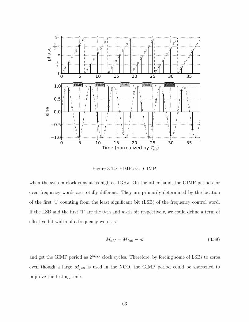
0 5 10 15 20 25 30 350
π
2
π
3
2π
2π
phas
e
0 5 10 15 20 25 30 35Time (normalized by Tclk)
1.0
0.5
0.0
0.5
1.0
sine
FIMP FIMP FIMP FIMP GIMP
Figure 3.14: FIMPs vs. GIMP.
when the system clock runs at as high as 1GHz. On the other hand, the GIMP periods for
even frequency words are totally different. They are primarily determined by the location
of the first ‘1’ counting from the least significant bit (LSB) of the frequency control word.
If the LSB and the first ‘1’ are the 0-th and m-th bit respectively, we could define a term of
effective bit-width of a frequency word as
Meff = Mfull −m (3.39)
and get the GIMP period as 2Meff clock cycles. Therefore, by forcing some of LSBs to zeros
even though a large Mfull is used in the NCO, the GIMP period could be shortened to
improve the testing time.
63

D Q
carry
clk
f
GIMP
Phase Word
Phase Accumulator
D Q
Mfull
Mfull
MfullMfullMfullMfull
Figure 3.15: GIMP detector.
3.3.2 Frequency Response Measurement in SSA-based ORA
Although the FIMP accumulation does introduce errors as discussed earlier, it is still
chosen for frequency response measurement. There are mainly two reasons. First, the
DUT is driven by a 1-tone signal and its ouput will be measured at the same frequency,
where the strongest spectrum would locate itself. Thus, the FIMP errors are expected to be
negligible for most cases. If not, as given in Section 3.2.1, increasing the number of FIMPs
to stop accumulation would help to further suppress the errors. Second, since frequency
response measurement is usually done at many frequency points, testing time would increase
drastically if GIMP accumulation were used. Therefore, FIMPs, instead of GIMPs, are used
for frequency response measurement. In addition, as proven in Section 3.2.1, the half FIMPs
(HFIMPs) could be used to further shorten the test time. The HFIMPs could be captured by
the FIMP detector in Figure 3.13 if the carry out signal is replaced with the most significant
bit (MSB) of the phase accumulator.
It should be noted the phase accumulator used in the IMP circuit is in NCO1, so there
is no need for extra hardware except the effort of pulling out the MSB from the phase
accumulator.
The proposed HFIMP circuit was simulated for its performance. The ORA is used to
measure two DUTs’ frequency responses in simulation, where the differences between the
magnitude and phase responses of two DUTs, ∆Asim and ∆φsim, are known beforehand.
64
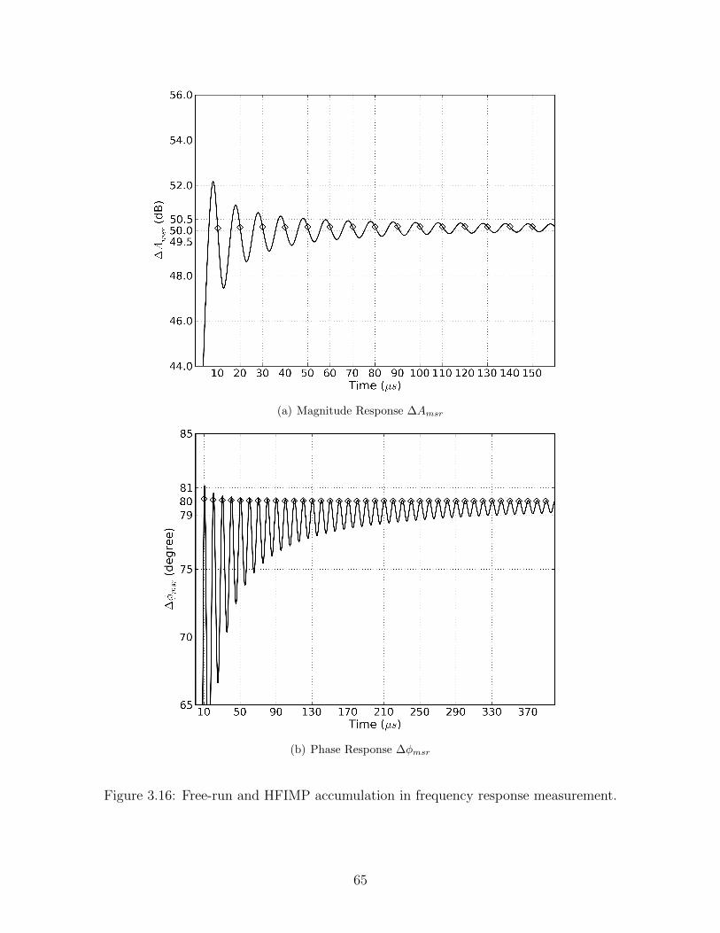
(a) Magnitude Response ∆Amsr
(b) Phase Response ∆φmsr
Figure 3.16: Free-run and HFIMP accumulation in frequency response measurement.
65
In order to accurately characterize the frequency responses of these two DUTs, both the
measured ∆Amsr and ∆φmsr need to satisfy
∆Asim −∆Atol ≤ ∆Amsr ≤ ∆Asim + ∆Atol
∆φsim −∆φtol ≤ ∆φmsr ≤ ∆φsim + ∆φtol (3.40)
where ∆Atol and ∆φtol are the desired accuracy tolerance for the magnitude and phase
response measurement, respectively.
One simulation, where one of the DUTs is 50 dB higher in magnitude and 80◦ earlier in
phase than the other one at 50kHz, was conducted as an example. The simulated ∆Amsr and
∆φmsr vs. test time are plotted in Figure 3.16 where the circle points represent the HFIMPs
picked by the HFIMP circuit. According to the plots, for ∆Atol = 0.5dB and ∆φtol = 1◦,
the free-run accumulation requires 6 and 34 HFIMPs respectively to make the ∆Amsr and
∆φmsr curves converge into their own tolerance band. However, if HFIMPs are used to stop
accumulation, both ∆Amsr and ∆φmsr are guaranteed to be converged at the first HFIMP
location. Therefore, the test time can be shortened by using HFIMP accumulation without
sacrificing the accuracy of measurements. Furthermore, since the ORA is able to stop the
accumulation earlier than free-run accumulation, the size of the DC1 and DC2 accumulators
can be smaller. This means that the area overhead of the BIST circuitry is decreased with
IMP accumulation built in the ORA.
A comprehensive analysis was performed to study the measurement accuracy that could
be achieved by using HFIMP accumulation under different conditions. The possible combi-
nations of the simulation variables, distributed over the range of [Min., Max.] evenly within
a step, are listed in Table 3.2.
At each frequency, different combinations of ∆Asim and ∆φsim between the two DUTs
were simulated. Among them, the maximum measurement errors ∆Amsr − ∆Asim and
∆φmsr − ∆φsim were selected and plotted in Figure 3.17. For very low frequency below
66
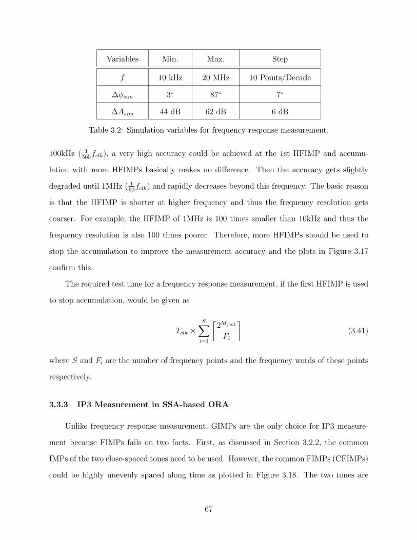
Variables Min. Max. Step
f 10 kHz 20 MHz 10 Points/Decade
∆φsim 3◦ 87◦ 7◦
∆Asim 44 dB 62 dB 6 dB
Table 3.2: Simulation variables for frequency response measurement.
100kHz ( 1500fclk), a very high accuracy could be achieved at the 1st HFIMP and accumu-
lation with more HFIMPs basically makes no difference. Then the accuracy gets slightly
degraded until 1MHz ( 150fclk) and rapidly decreases beyond this frequency. The basic reason
is that the HFIMP is shorter at higher frequency and thus the frequency resolution gets
coarser. For example, the HFIMP of 1MHz is 100 times smaller than 10kHz and thus the
frequency resolution is also 100 times poorer. Therefore, more HFIMPs should be used to
stop the accumulation to improve the measurement accuracy and the plots in Figure 3.17
confirm this.
The required test time for a frequency response measurement, if the first HFIMP is used
to stop accumulation, would be given as
Tclk ×S∑i=1
⌈2Mfull
Fi
⌉(3.41)
where S and Fi are the number of frequency points and the frequency words of these points
respectively.
3.3.3 IP3 Measurement in SSA-based ORA
Unlike frequency response measurement, GIMPs are the only choice for IP3 measure-
ment because FIMPs fails on two facts. First, as discussed in Section 3.2.2, the common
IMPs of the two close-spaced tones need to be used. However, the common FIMPs (CFIMPs)
could be highly unevenly spaced along time as plotted in Figure 3.18. The two tones are
67
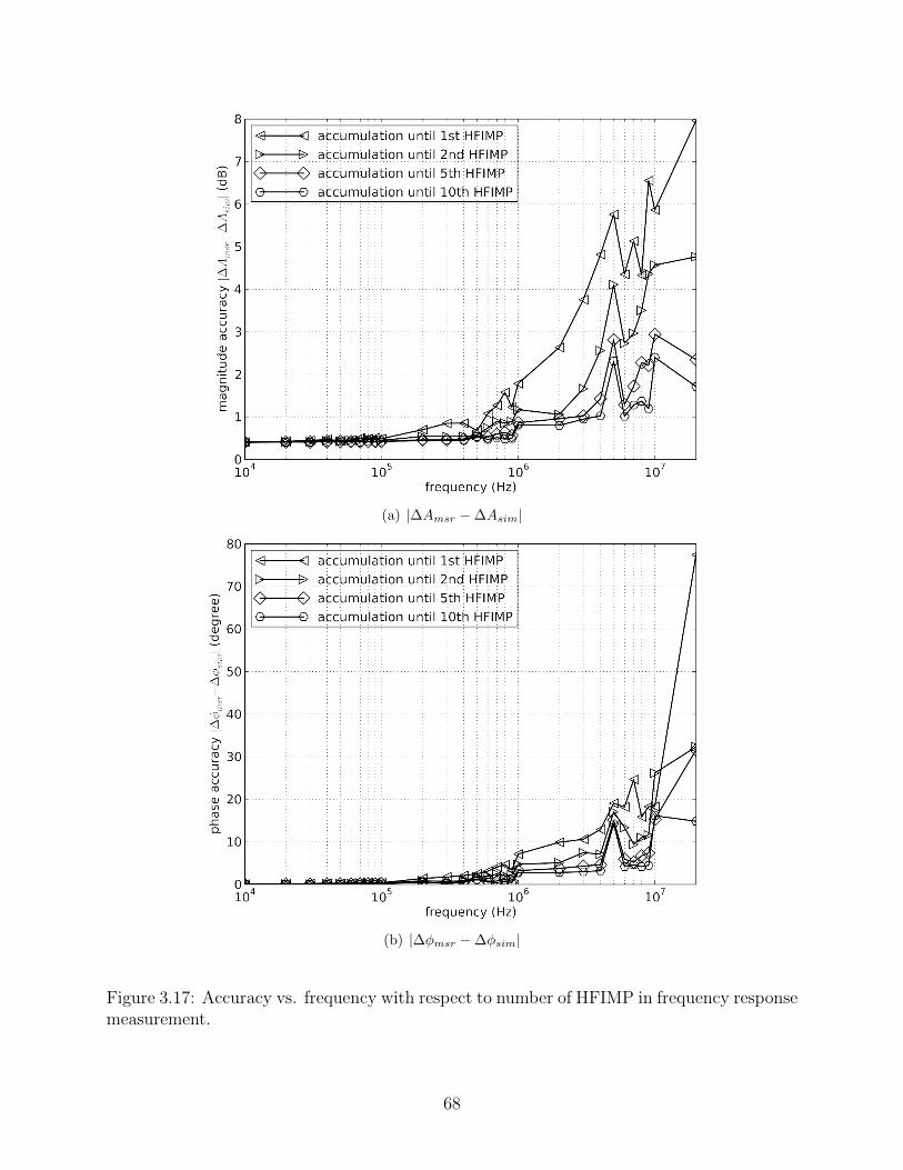
(a) |∆Amsr −∆Asim|
(b) |∆φmsr −∆φsim|
Figure 3.17: Accuracy vs. frequency with respect to number of HFIMP in frequency responsemeasurement.
68
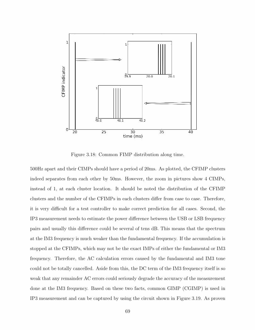
Figure 3.18: Common FIMP distribution along time.
500Hz apart and their CIMPs should have a period of 20ms. As plotted, the CFIMP clusters
indeed separates from each other by 50ms. However, the zoom in pictures show 4 CIMPs,
instead of 1, at each cluster location. It should be noted the distribution of the CFIMP
clusters and the number of the CFIMPs in each clusters differ from case to case. Therefore,
it is very difficult for a test controller to make correct prediction for all cases. Second, the
IP3 measurement needs to estimate the power difference between the USB or LSB frequency
pairs and usually this difference could be several of tens dB. This means that the spectrum
at the IM3 frequency is much weaker than the fundamental frequency. If the accumulation is
stopped at the CFIMPs, which may not be the exact IMPs of either the fundamental or IM3
frequency. Therefore, the AC calculation errors caused by the fundamental and IM3 tone
could not be totally cancelled. Aside from this, the DC term of the IM3 frequency itself is so
weak that any remainder AC errors could seriously degrade the accuracy of the measurement
done at the IM3 frequency. Based on these two facts, common GIMP (CGIMP) is used in
IP3 measurement and can be captured by using the circuit shown in Figure 3.19. As proven
69
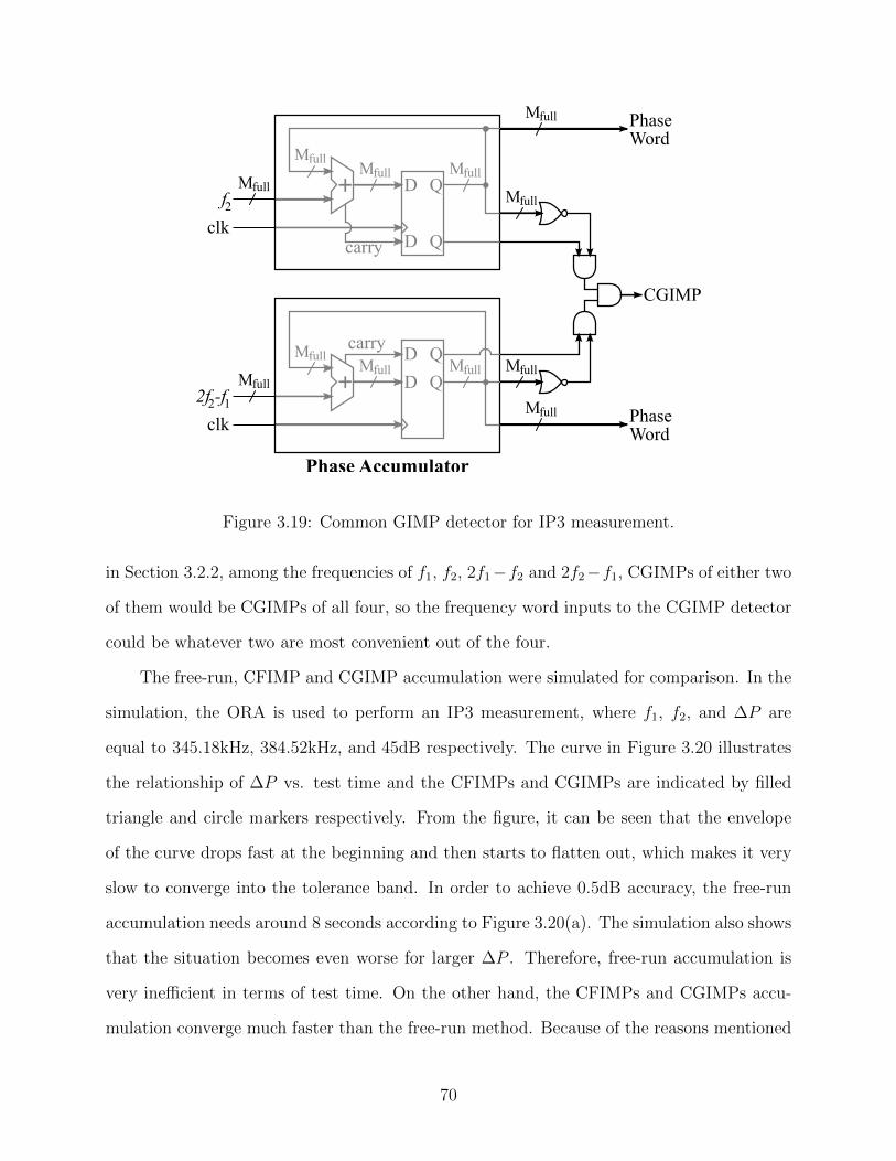
D Q
carry
clk
2f -f
CGIMP
Phase Word
Phase Accumulator
D Q
D Q
carryclk
f
Phase Word
D Q
2 1
2
Mfull
Mfull
MfullMfull Mfull
MfullMfull Mfull Mfull
Mfull
Mfull
Mfull
Figure 3.19: Common GIMP detector for IP3 measurement.
in Section 3.2.2, among the frequencies of f1, f2, 2f1−f2 and 2f2−f1, CGIMPs of either two
of them would be CGIMPs of all four, so the frequency word inputs to the CGIMP detector
could be whatever two are most convenient out of the four.
The free-run, CFIMP and CGIMP accumulation were simulated for comparison. In the
simulation, the ORA is used to perform an IP3 measurement, where f1, f2, and ∆P are
equal to 345.18kHz, 384.52kHz, and 45dB respectively. The curve in Figure 3.20 illustrates
the relationship of ∆P vs. test time and the CFIMPs and CGIMPs are indicated by filled
triangle and circle markers respectively. From the figure, it can be seen that the envelope
of the curve drops fast at the beginning and then starts to flatten out, which makes it very
slow to converge into the tolerance band. In order to achieve 0.5dB accuracy, the free-run
accumulation needs around 8 seconds according to Figure 3.20(a). The simulation also shows
that the situation becomes even worse for larger ∆P . Therefore, free-run accumulation is
very inefficient in terms of test time. On the other hand, the CFIMPs and CGIMPs accu-
mulation converge much faster than the free-run method. Because of the reasons mentioned
70
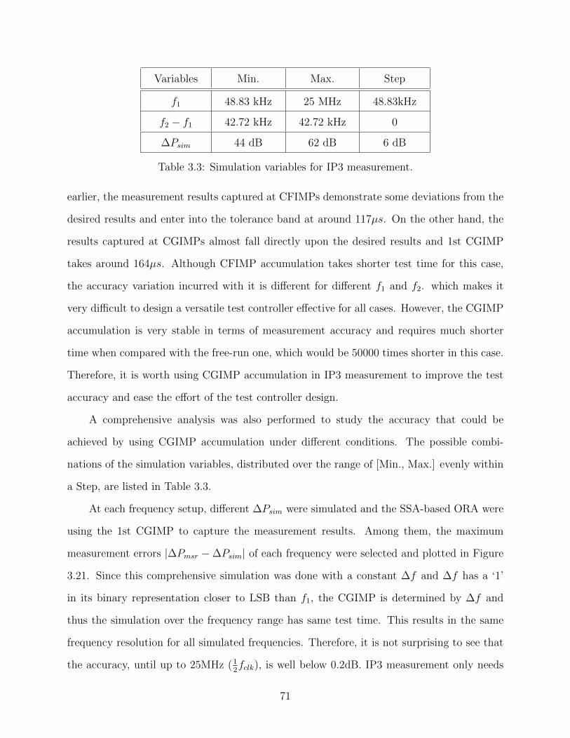
Variables Min. Max. Step
f1 48.83 kHz 25 MHz 48.83kHz
f2 − f1 42.72 kHz 42.72 kHz 0
∆Psim 44 dB 62 dB 6 dB
Table 3.3: Simulation variables for IP3 measurement.
earlier, the measurement results captured at CFIMPs demonstrate some deviations from the
desired results and enter into the tolerance band at around 117µs. On the other hand, the
results captured at CGIMPs almost fall directly upon the desired results and 1st CGIMP
takes around 164µs. Although CFIMP accumulation takes shorter test time for this case,
the accuracy variation incurred with it is different for different f1 and f2. which makes it
very difficult to design a versatile test controller effective for all cases. However, the CGIMP
accumulation is very stable in terms of measurement accuracy and requires much shorter
time when compared with the free-run one, which would be 50000 times shorter in this case.
Therefore, it is worth using CGIMP accumulation in IP3 measurement to improve the test
accuracy and ease the effort of the test controller design.
A comprehensive analysis was also performed to study the accuracy that could be
achieved by using CGIMP accumulation under different conditions. The possible combi-
nations of the simulation variables, distributed over the range of [Min., Max.] evenly within
a Step, are listed in Table 3.3.
At each frequency setup, different ∆Psim were simulated and the SSA-based ORA were
using the 1st CGIMP to capture the measurement results. Among them, the maximum
measurement errors |∆Pmsr −∆Psim| of each frequency were selected and plotted in Figure
3.21. Since this comprehensive simulation was done with a constant ∆f and ∆f has a ‘1’
in its binary representation closer to LSB than f1, the CGIMP is determined by ∆f and
thus the simulation over the frequency range has same test time. This results in the same
frequency resolution for all simulated frequencies. Therefore, it is not surprising to see that
the accuracy, until up to 25MHz (12fclk), is well below 0.2dB. IP3 measurement only needs
71
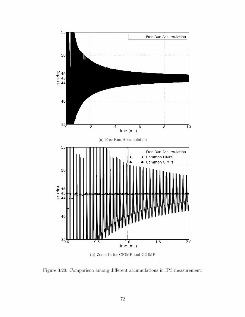
(a) Free-Run Accumulation
(b) Zoom-In for CFIMP and CGIMP
Figure 3.20: Comparison among different accumulations in IP3 measurement.
72
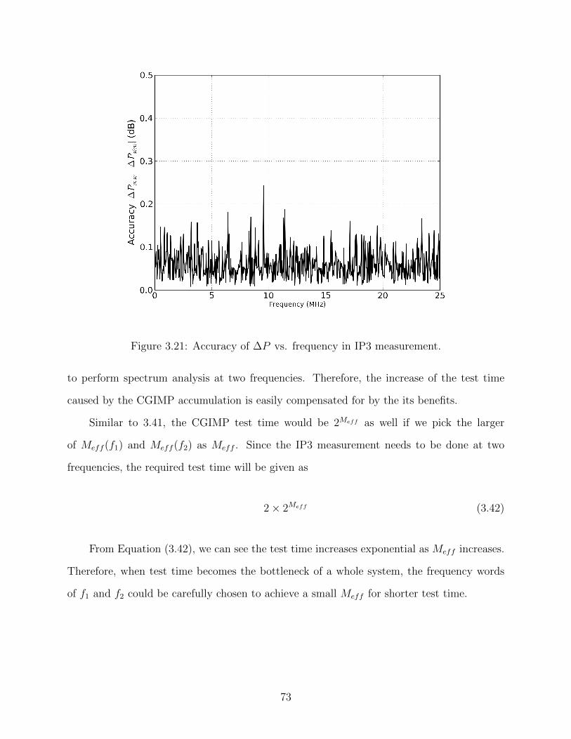
Figure 3.21: Accuracy of ∆P vs. frequency in IP3 measurement.
to perform spectrum analysis at two frequencies. Therefore, the increase of the test time
caused by the CGIMP accumulation is easily compensated for by the its benefits.
Similar to 3.41, the CGIMP test time would be 2Meff as well if we pick the larger
of Meff (f1) and Meff (f2) as Meff . Since the IP3 measurement needs to be done at two
frequencies, the required test time will be given as
2× 2Meff (3.42)
From Equation (3.42), we can see the test time increases exponential as Meff increases.
Therefore, when test time becomes the bottleneck of a whole system, the frequency words
of f1 and f2 could be carefully chosen to achieve a small Meff for shorter test time.
73

3.3.4 Noise and Spur Measurement in SSA-based ORA
In noise and spur measurement, the DUT is simulated with a 1-tone input signal and
the ORA performs a sweep-type spectrum analysis at output. It has a similar test setup
as the frequency response measurement. However, its nature is almost identical to IP3
measurement. First, the spectrum analysis is done at a frequency different from the frequency
where the strongest tone is located. Second, the spectrum at the interested frequencies is
much weaker than the strongest tone. Therefore, the accumulation has to be stopped at
the common GIMPs of the frequency sweeping step ∆f and tone frequency to cancel off the
AC calculation. Since the simulation set up is almost identical to the IP3 measurement, no
separate experimental results are included in the paper. The required test time for them
could also be given by an equation similar to Equation (3.42)
S × 2Meff (3.43)
where S is the number of frequency points in measurement.
3.3.5 Comparison between the SSA and FFT based ORAs
The SSA-based ORA was modeled with parameterized number of input bits (N , which
corresponds to the number of multiplier bits) and number of output bits (W , which corre-
sponds the number of accumulator bits) to support the requirement for tested signal with
varied bit-width. In our implementation, the BIST circuitry is synthesized into a Xilinx
Spartan-3 XC3S200 FPGA. Table 3.4 summarizes the number of slices and LUTs (which are
listed in left and right column respectively) required for implementing a MAC as a function
of different values for N and W . As can be seen, when W increases, the logic required to
realize the accumulator will increase correspondingly. Table 3.4 shows a perfect linear rela-
tionship between the resource usage and W if N is fixed. In fact, the accumulator requires
exactly one slice for every two bits of the accumulator. However, when increasing size, the
74
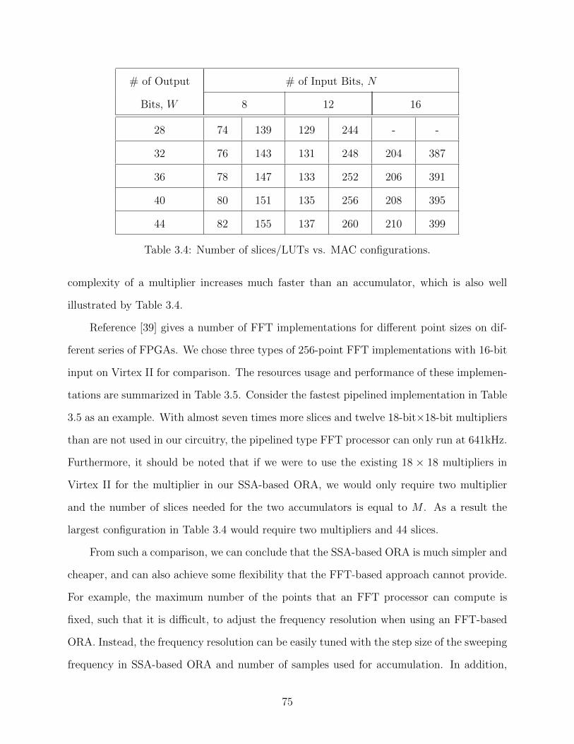
# of Output # of Input Bits, N
Bits, W 8 12 16
28 74 139 129 244 - -
32 76 143 131 248 204 387
36 78 147 133 252 206 391
40 80 151 135 256 208 395
44 82 155 137 260 210 399
Table 3.4: Number of slices/LUTs vs. MAC configurations.
complexity of a multiplier increases much faster than an accumulator, which is also well
illustrated by Table 3.4.
Reference [39] gives a number of FFT implementations for different point sizes on dif-
ferent series of FPGAs. We chose three types of 256-point FFT implementations with 16-bit
input on Virtex II for comparison. The resources usage and performance of these implemen-
tations are summarized in Table 3.5. Consider the fastest pipelined implementation in Table
3.5 as an example. With almost seven times more slices and twelve 18-bit×18-bit multipliers
than are not used in our circuitry, the pipelined type FFT processor can only run at 641kHz.
Furthermore, it should be noted that if we were to use the existing 18 × 18 multipliers in
Virtex II for the multiplier in our SSA-based ORA, we would only require two multiplier
and the number of slices needed for the two accumulators is equal to M . As a result the
largest configuration in Table 3.4 would require two multipliers and 44 slices.
From such a comparison, we can conclude that the SSA-based ORA is much simpler and
cheaper, and can also achieve some flexibility that the FFT-based approach cannot provide.
For example, the maximum number of the points that an FFT processor can compute is
fixed, such that it is difficult, to adjust the frequency resolution when using an FFT-based
ORA. Instead, the frequency resolution can be easily tuned with the step size of the sweeping
frequency in SSA-based ORA and number of samples used for accumulation. In addition,
75
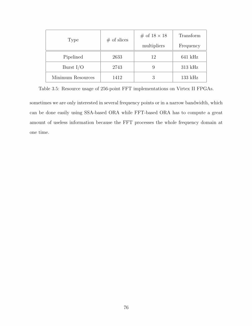
Type # of slices# of 18× 18 Transform
multipliers Frequency
Pipelined 2633 12 641 kHz
Burst I/O 2743 9 313 kHz
Minimum Resources 1412 3 133 kHz
Table 3.5: Resource usage of 256-point FFT implementations on Virtex II FPGAs.
sometimes we are only interested in several frequency points or in a narrow bandwidth, which
can be done easily using SSA-based ORA while FFT-based ORA has to compute a great
amount of useless information because the FFT processes the whole frequency domain at
one time.
76
Chapter 4
CORDIC based Test Pattern Generator
In the proposed mixed-signal BIST approach, DDS is employed to implement the TPG.
A high-speed DDS with a clean spectrum is always desired to produce high-quality test
stimulus. The NCO, as one of the critical components in DDS, is conventionally implemented
with a hardware look-up table (LUT). However, when the bit width of the DAC increases, the
hardware resources required for building the LUT will increase exponentially. Furthermore,
it is also difficult to guarantee the speed of a LUT as its size becomes large. Therefore,
alternative strategies have to be employed for high-speed and fine-resolution NCO design.
The CORDIC (COordinate Rotation DIgital Computer) is an ROM-less iterative algorithm
which is able to calculate several elementary functions, including sine and cosine, by just
using bit shift and add operations. However, it is not widely used in NCO design since it
is slower and consumes more hardware resources than other LUT compression techniques.
This chapter revisits CORDIC algorithm and proposes several techniques to accelerate its
speed while keeping a relatively low area overhead for its actual hardware implementation.
4.1 Introduction to Direct Digital Synthesis (DDS)
4.1.1 General Architecture and Design Concerns of DDS
As illustrated in Figure 4.1, a typical DDS is usually composed of a NCO, a DAC, and
an LPF. The NCO consists of a phase accumulator and a phase-to-sin/cos conversion unit.
The phase accumulator increases its value by the FCW input every clock cycle and produces
a linear Mfull-bit phase output, which will be truncated to M bits and then mapped to a N -
bit digital sinusoidal waveform by the conversion unit. The conventional way to implement
this conversion unit is to construct the mapping relationship between the phase and sin/cos
77

D Q Phase toSin/Cos
DACFCWN
Numerically Controlled Oscillator
fclk
fsin/cos
Pha
seT
runc
atio
n
Mfull M
Figure 4.1: Diagram for a typical DDS system.
function in a hardware LUT. A DAC is employed right after the NCO to translate the
digital signal into a analog waveform, which exhibits a great amount of undesired frequency
components outside of the bandwidth [0, fclk2
] because of its step-wise nature. In order to
filter out these frequency components to achieve a smooth and clean sinusoidal waveform,
it is a common practice to include an LPF in a DDS system. The output frequency of the
DDS can be expressed as
fsin/cos =FCW
2Mfullfclk (4.1)
Unlike the analog frequency synthesizers such as phase locked loop (PLL) , all the
signals in a NCO are in digital form, so one of major advantages that the DDS can offer is
the ability to precisely and rapidly manipulate its output frequency, amplitude, and phase
through digital control [40]. However, the DDS also suffers from quantization noise caused
by the finite word length effect. For example, the signal-to-quantization noise ratio of a
N -bit digital system could be given as [38]
SNR ≈ 6.02 ·N + 1.76. (4.2)
Just like any other engineering systems, DDS also needs to be designed against its
performance specification, which basically defines the freedom space for designers. Some
78
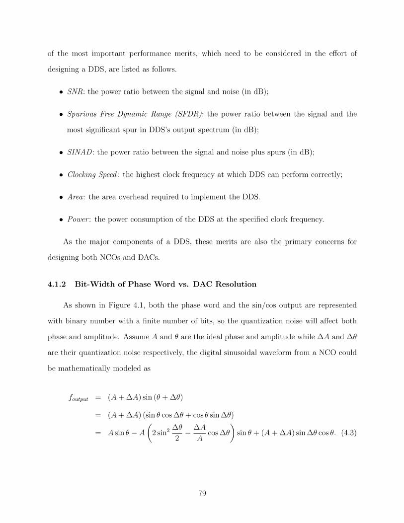
of the most important performance merits, which need to be considered in the effort of
designing a DDS, are listed as follows.
• SNR: the power ratio between the signal and noise (in dB);
• Spurious Free Dynamic Range (SFDR): the power ratio between the signal and the
most significant spur in DDS’s output spectrum (in dB);
• SINAD : the power ratio between the signal and noise plus spurs (in dB);
• Clocking Speed : the highest clock frequency at which DDS can perform correctly;
• Area: the area overhead required to implement the DDS.
• Power : the power consumption of the DDS at the specified clock frequency.
As the major components of a DDS, these merits are also the primary concerns for
designing both NCOs and DACs.
4.1.2 Bit-Width of Phase Word vs. DAC Resolution
As shown in Figure 4.1, both the phase word and the sin/cos output are represented
with binary number with a finite number of bits, so the quantization noise will affect both
phase and amplitude. Assume A and θ are the ideal phase and amplitude while ∆A and ∆θ
are their quantization noise respectively, the digital sinusoidal waveform from a NCO could
be mathematically modeled as
foutput = (A+ ∆A) sin (θ + ∆θ)
= (A+ ∆A) (sin θ cos ∆θ + cos θ sin ∆θ)
= A sin θ − A(
2 sin2 ∆θ
2− ∆A
Acos ∆θ
)sin θ + (A+ ∆A) sin ∆θ cos θ. (4.3)
79
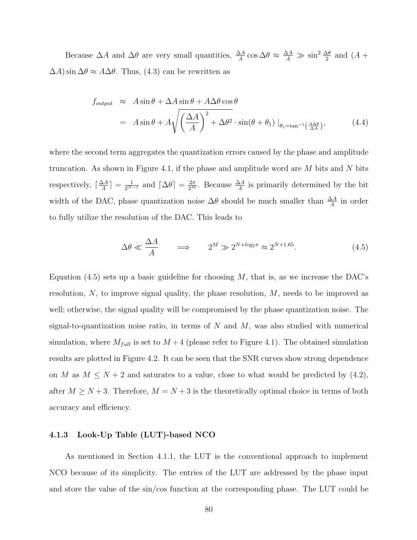
Because ∆A and ∆θ are very small quantities, ∆AA
cos ∆θ ≈ ∆AA� sin2 ∆θ
2and (A +
∆A) sin ∆θ ≈ A∆θ. Thus, (4.3) can be rewritten as
foutput ≈ A sin θ + ∆A sin θ + A∆θ cos θ
= A sin θ + A
√(∆A
A
)2
+ ∆θ2 · sin(θ + θ1) |θ1=tan−1(A∆θ∆A ), (4.4)
where the second term aggregates the quantization errors caused by the phase and amplitude
truncation. As shown in Figure 4.1, if the phase and amplitude word are M bits and N bits
respectively, d∆AAe = 1
2N−1 and d∆θe = 2π2M
. Because ∆AA
is primarily determined by the bit
width of the DAC, phase quantization noise ∆θ should be much smaller than ∆AA
in order
to fully utilize the resolution of the DAC. This leads to
∆θ � ∆A
A=⇒ 2M � 2N+log2π ≈ 2N+1.65. (4.5)
Equation (4.5) sets up a basic guideline for choosing M , that is, as we increase the DAC’s
resolution, N , to improve signal quality, the phase resolution, M , needs to be improved as
well; otherwise, the signal quality will be compromised by the phase quantization noise. The
signal-to-quantization noise ratio, in terms of N and M , was also studied with numerical
simulation, where Mfull is set to M + 4 (please refer to Figure 4.1). The obtained simulation
results are plotted in Figure 4.2. It can be seen that the SNR curves show strong dependence
on M as M ≤ N + 2 and saturates to a value, close to what would be predicted by (4.2),
after M ≥ N + 3. Therefore, M = N + 3 is the theoretically optimal choice in terms of both
accuracy and efficiency.
4.1.3 Look-Up Table (LUT)-based NCO
As mentioned in Section 4.1.1, the LUT is the conventional approach to implement
NCO because of its simplicity. The entries of the LUT are addressed by the phase input
and store the value of the sin/cos function at the corresponding phase. The LUT could be
80

N - 2 N - 1 N N + 1 N + 2 N + 3 N + 4 N + 5 N + 6Bit-width of Phase Word: M
10
20
30
40
50
60
70
80
90
100
Sig
nal-
to-Q
uanti
zati
on N
ois
e R
ati
o (
dB
)
N = 6
N = 8
N = 10
N = 12
N = 14
N = 16
Figure 4.2: Signal-to-quantization noise ratio vs. (N, M).
implemented by using read-only memory (ROM) or hard-wired combinational logic and its
area overhead is primarily determined by the bit-width of the amplitude and phase word, N
and M . Utilizing the symmetrical nature of the sin/cos functions, the LUT-based NCO can
offer quadrature output by storing only the value of sin(θ) |0◦≤θ<45◦ and cos(θ) |0◦≤θ<45◦ in
two tables1. Such a NCO can be implemented as in Figure 4.3. First, the phase θ |0◦≤θ<360◦
from the accumulator will be mapped to a phase θ′ |0◦≤θ′<90◦ by the quadrant MUX. Then
the two LUTs, which store the sine and cosine table from 0◦ to 45◦ respectively, cooperate
with the 45◦ MUX to find the corresponding sine and cosine value for θ′. This operation
relies on the symmetry between the sin and cos function in the first quadrant. Finally, the
sign of the sin and cos output will be determined based on the quadrant of the phase θ
through the sign MUX.
1in fact these two tables together store the same information as cos(θ) |0◦≤θ<90◦ or sin(θ) |0◦≤θ<90◦
81
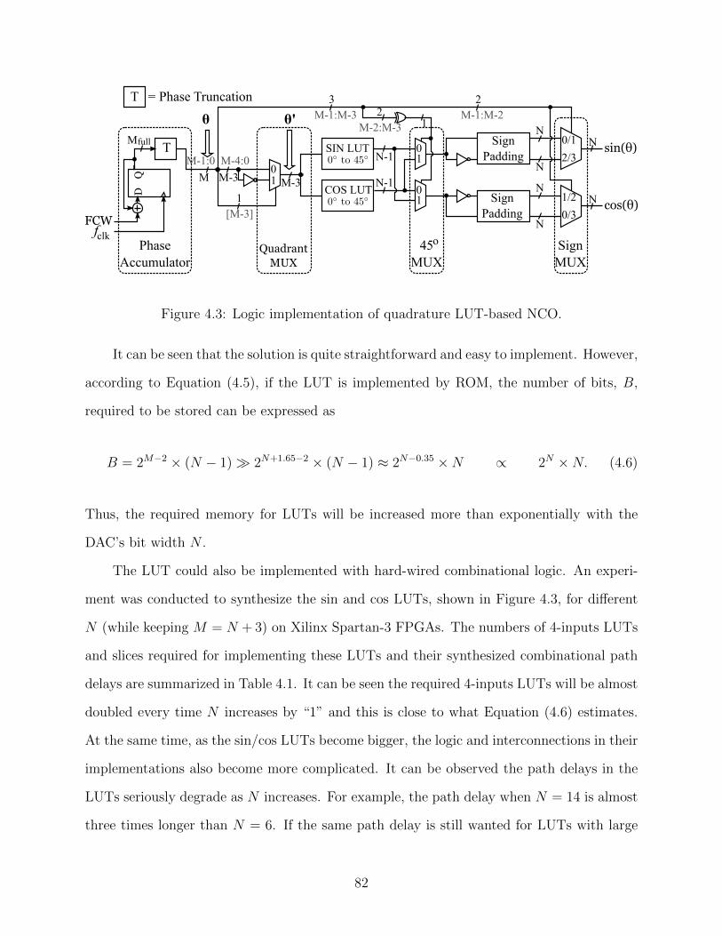
DQ
FCWfclk
01
SIN LUT
COS LUT
01
01
Phase Accumulator
M M-3
2
M-4:0
M-3
Quadrant MUX
N-1
N-11
Sign Padding
Sign Padding
45 MUX
o
3M-1:M-3
2M-1:M-2
1
[M-3]
0/1
2/3
1/2
0/3
N
N
N
N
N
N
Sign MUX
M-2:M-3
sin(θ)
cos(θ)
M-1:0
T = Phase Truncation
Mfull
θ'θ
T
Figure 4.3: Logic implementation of quadrature LUT-based NCO.
It can be seen that the solution is quite straightforward and easy to implement. However,
according to Equation (4.5), if the LUT is implemented by ROM, the number of bits, B,
required to be stored can be expressed as
B = 2M−2 × (N − 1)� 2N+1.65−2 × (N − 1) ≈ 2N−0.35 ×N ∝ 2N ×N. (4.6)
Thus, the required memory for LUTs will be increased more than exponentially with the
DAC’s bit width N .
The LUT could also be implemented with hard-wired combinational logic. An experi-
ment was conducted to synthesize the sin and cos LUTs, shown in Figure 4.3, for different
N (while keeping M = N + 3) on Xilinx Spartan-3 FPGAs. The numbers of 4-inputs LUTs
and slices required for implementing these LUTs and their synthesized combinational path
delays are summarized in Table 4.1. It can be seen the required 4-inputs LUTs will be almost
doubled every time N increases by “1” and this is close to what Equation (4.6) estimates.
At the same time, as the sin/cos LUTs become bigger, the logic and interconnections in their
implementations also become more complicated. It can be observed the path delays in the
LUTs seriously degrade as N increases. For example, the path delay when N = 14 is almost
three times longer than N = 6. If the same path delay is still wanted for LUTs with large
82
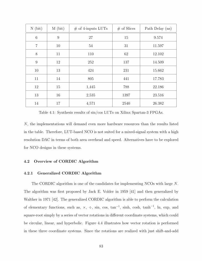
N (bit) M (bit) # of 4-inputs LUTs # of Slices Path Delay (ns)
6 9 27 15 9.574
7 10 54 31 11.597
8 11 110 62 12.102
9 12 252 137 14.509
10 13 424 231 15.662
11 14 805 441 17.783
12 15 1,445 788 22.186
13 16 2,535 1397 23.516
14 17 4,571 2540 26.382
Table 4.1: Synthesis results of sin/cos LUTs on Xilinx Spartan-3 FPGAs.
N , the implementations will demand even more hardware resources than the results listed
in the table. Therefore, LUT-based NCO is not suited for a mixed-signal system with a high
resolution DAC in terms of both area overhead and speed. Alternatives have to be explored
for NCO designs in these systems.
4.2 Overview of CORDIC Algorithm
4.2.1 Generalized CORDIC Algorithm
The CORDIC algorithm is one of the candidates for implementing NCOs with large N .
The algorithm was first proposed by Jack E. Volder in 1959 [41] and then generalized by
Walther in 1971 [42]. The generalized CORDIC algorithm is able to perform the calculation
of elementary functions, such as, ×, ÷, sin, cos, tan−1, sinh, cosh, tanh−1, ln, exp, and
square-root simply by a series of vector rotations in different coordinate systems, which could
be circular, linear, and hyperbolic. Figure 4.4 illustrates how vector rotation is performed
in these three coordinate systems. Since the rotations are realized with just shift-and-add
83

x
y
x
y
x
y
circular rotation linear rotation hyperbolic rotation
Figure 4.4: Illustration of vector rotation in different coordinate systems.
(or shift-and-subtract) operations, the CORDIC can be implemented iteratively without
the involvement of multipliers. Such a feature makes the CORDIC a preferable choice for
hardware logic implementation. The mathematic expression of the vector rotation at the
i-th iteration is given by
xi+1 = xi −mσi2−Sm,iyi, (4.7a)
yi+1 = yi + σi2−Sm,ixi, (4.7b)
zi+1 = zi − σiαm,i, (4.7c)
where σi represents the rotation direction (clockwise and counter-clockwise for −1 and +1,
respectively), m decides the choice of the coordinate systems (circular, linear, and hyperbolic
for m = 1, 0,−1 respectively), Sm,i is a non-decreasing integer shift sequence, and αm,i
denotes the elementary rotation angle and could be obtained through
αm,i =1√m
tan−1(√m2−Sm,i). (4.8)
The generalized CORDIC algorithm supports two operational modes, rotation and vec-
toring, and each of them has different iteration goal. In the rotation mode the CORDIC
treats z0 as system input and its goal is to make z as close as possible to 0 through iterations.
84
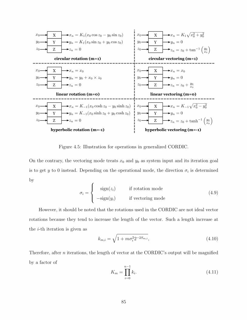
X
Y
Z
circular rotation (m=1)
X
Y
Z
circular vectoring (m=1)
X
Y
Z
linear vectoring (m=0)
X
Y
Z
hyperbolic vectoring (m=-1)
X
Y
Z
linear rotation (m=0)
X
Y
Z
hyperbolic rotation (m=-1)
Figure 4.5: Illustration for operations in generalized CORDIC.
On the contrary, the vectoring mode treats x0 and y0 as system input and its iteration goal
is to get y to 0 instead. Depending on the operational mode, the direction σi is determined
by
σi =
sign(zi) if rotation mode
−sign(yi) if vectoring mode(4.9)
However, it should be noted that the rotations used in the CORDIC are not ideal vector
rotations because they tend to increase the length of the vector. Such a length increase at
the i-th iteration is given as
km,i =√
1 +mσ2i 2−2Sm,i , (4.10)
Therefore, after n iterations, the length of vector at the CORDIC’s output will be magnified
by a factor of
Km =n−1∏i=0
ki. (4.11)
85
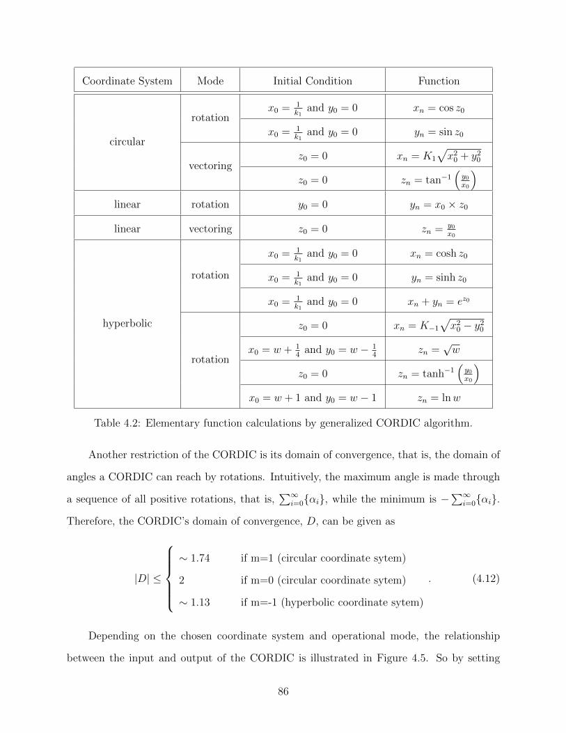
Coordinate System Mode Initial Condition Function
circular
rotationx0 = 1
k1and y0 = 0 xn = cos z0
x0 = 1k1
and y0 = 0 yn = sin z0
vectoringz0 = 0 xn = K1
√x2
0 + y20
z0 = 0 zn = tan−1(y0
x0
)linear rotation y0 = 0 yn = x0 × z0
linear vectoring z0 = 0 zn = y0
x0
hyperbolic
rotation
x0 = 1k1
and y0 = 0 xn = cosh z0
x0 = 1k1
and y0 = 0 yn = sinh z0
x0 = 1k1
and y0 = 0 xn + yn = ez0
rotation
z0 = 0 xn = K−1
√x2
0 − y20
x0 = w + 14
and y0 = w − 14
zn =√w
z0 = 0 zn = tanh−1(y0
x0
)x0 = w + 1 and y0 = w − 1 zn = lnw
Table 4.2: Elementary function calculations by generalized CORDIC algorithm.
Another restriction of the CORDIC is its domain of convergence, that is, the domain of
angles a CORDIC can reach by rotations. Intuitively, the maximum angle is made through
a sequence of all positive rotations, that is,∑∞
i=0{αi}, while the minimum is −∑∞
i=0{αi}.
Therefore, the CORDIC’s domain of convergence, D, can be given as
|D| ≤
∼ 1.74 if m=1 (circular coordinate sytem)
2 if m=0 (circular coordinate sytem)
∼ 1.13 if m=-1 (hyperbolic coordinate sytem)
. (4.12)
Depending on the chosen coordinate system and operational mode, the relationship
between the input and output of the CORDIC is illustrated in Figure 4.5. So by setting
86
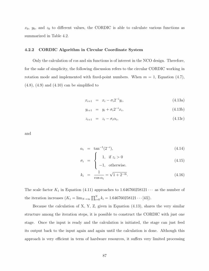
x0, y0, and z0 to different values, the CORDIC is able to calculate various functions as
summarized in Table 4.2.
4.2.2 CORDIC Algorithm in Circular Coordinate System
Only the calculation of cos and sin functions is of interest in the NCO design. Therefore,
for the sake of simplicity, the following discussion refers to the circular CORDIC working in
rotation mode and implemented with fixed-point numbers. When m = 1, Equation (4.7),
(4.8), (4.9) and (4.10) can be simplified to
xi+1 = xi − σi2−iyi, (4.13a)
yi+1 = yi + σi2−ixi, (4.13b)
zi+1 = zi − σiαi, (4.13c)
and
αi = tan−1(2−i), (4.14)
σi =
1, if zi > 0
−1, otherwise.(4.15)
ki =1
cosαi=√
1 + 2−2i. (4.16)
The scale factor K1 in Equation (4.11) approaches to 1.646760258121 · · · as the number of
the iteration increases (K1 = limN→∞∏N
i=0 ki = 1.646760258121 · · · [43]).
Because the calculation of X, Y, Z, given in Equation (4.13), shares the very similar
structure among the iteration steps, it is possible to construct the CORDIC with just one
stage. Once the input is ready and the calculation is initiated, the stage can just feed
its output back to the input again and again until the calculation is done. Although this
approach is very efficient in term of hardware resources, it suffers very limited processing
87
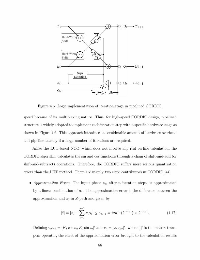
-1
-1
SignDetection
-1
>>i
>>i
01
01
0
1
D1
D2
D3
Q1
Q2
Q3
clk
Hard-WiredShift
Hard-WiredShift
Figure 4.6: Logic implementation of iteration stage in pipelined CORDIC.
speed because of its multiplexing nature. Thus, for high-speed CORDIC design, pipelined
structure is widely adopted to implement each iteration step with a specific hardware stage as
shown in Figure 4.6. This approach introduces a considerable amount of hardware overhead
and pipeline latency if a large number of iterations are required.
Unlike the LUT-based NCO, which does not involve any real on-line calculation, the
CORDIC algorithm calculates the sin and cos functions through a chain of shift-and-add (or
shift-and-subtract) operations. Therefore, the CORDIC suffers more serious quantization
errors than the LUT method. There are mainly two error contributors in CORDIC [44],
• Approximation Error : The input phase z0, after n iteration steps, is approximated
by a linear combination of αi. The approximation error is the difference between the
approximation and z0 in Z-path and given by
|δ| = |z0 −n−1∑i=0
σiαi| ≤ αn−1 = tan−1(2−n+1) < 2−n+1. (4.17)
Defining videal = [K1 cos z0, K1 sin z0]t and vn = [xn, yn]t, where [·]t is the matrix trans-
pose operator, the effect of the approximation error brought to the calculation results
88

is bounded by
|vn − videal||videal|
≤ 2 sin∣∣∣σ2
∣∣∣ ≤ αn−1 < 2−n+1. (4.18)
• Rounding Error : The calculation on the X-path and Y -path also introduces rounding
errors due to the finite word length effect. The rounding errors in each iteration stage
consists of two components: the ones propagated from previous stages and the ones
newly generated in the current stage. The two components mix themselves together
and propagate to latter stages. The rounding error present at the output is additive
to the ideal calculation results and bounded by
|f(n)| ≤√
2 · 2−N(
1 +n−1∑j=1
n−1∏i=j
k1(i)
)= 2−N+0.5
(1 +
n−1∑j=1
n−1∏i=j
k1(i)
), (4.19)
where N is the number of bits used to represent the data on the X and Y path.
Considering the contribution from both the approximation error and rounding error,
the overall quantization error could be expressed as
|vn − videal| ≤ 2−n+1 · |videal|+ |f(n)|
≤ 2−n+1 ·K1 · |v0|+ 2−N+0.5
[1 +
n−1∑j=1
n−1∏i=j
k1(i)
]
= 2−n+1 + 2−N+0.5
[1 +
n−1∑j=1
n−1∏i=j
k1(i)
]. (4.20)
This equation indicates that given n iteration steps and N -bit words to store intermediate
results2, the effective number of bits in a CORDIC, Neff , is around
2−Neff ≈ 2−n+1 + 2−N+0.5
[1 +
n−1∑j=1
n−1∏i=j
k1(i)
]. (4.21)
2n ≤ N + 1, otherwise, X and Y paths take no effect because the second terms in Equation (4.13a) and(4.13b) become zeros.
89
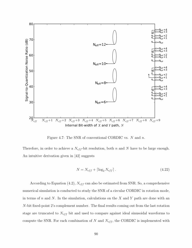
n=N n=N +1n=N +2
n=N +3n=N +4
n=N n=N +1n=N +2
n=N +3n=N +4
n=N
n=N +1n=N +2
n=N +3n=N +4
n=N
n=N +1n=N +2
n=N +3n=N +4
eff
effeff
effeff
eff
eff
eff
effeff
eff
effeff
effeff
eff
eff
eff
effeff
N =12
N =10
N =8
N =6
eff
eff
eff
eff
Figure 4.7: The SNR of conventional CORDIC vs. N and n.
Therefore, in order to achieve a Neff -bit resolution, both n and N have to be large enough.
An intuitive derivation given in [42] suggests
N = Neff + dlog2Neffe . (4.22)
According to Equation (4.2), Neff can also be estimated from SNR. So, a comprehensive
numerical simulation is conducted to study the SNR of a circular CORDIC in rotation mode,
in terms of n and N . In the simulation, calculations on the X and Y path are done with an
N -bit fixed-point 2’s complement number. The final results coming out from the last rotation
stage are truncated to Neff bit and used to compare against ideal sinusoidal waveforms to
compute the SNR. For each combination of N and Neff , the CORDIC is implemented with
90
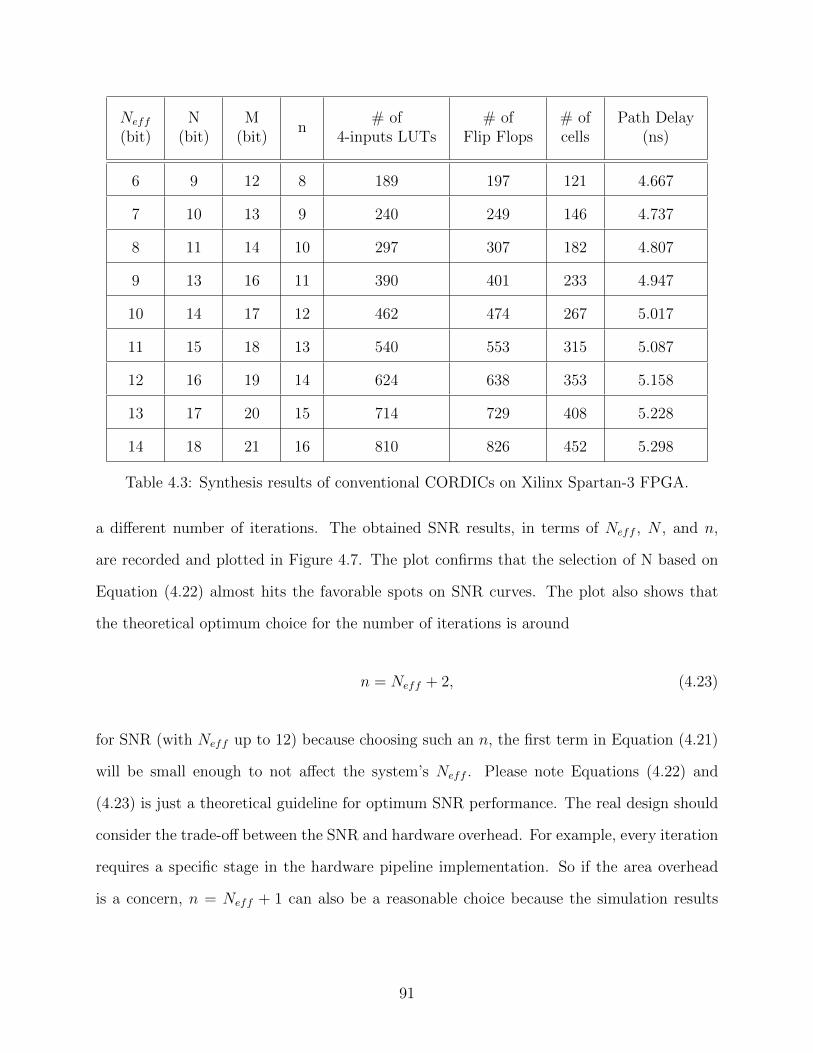
Neff
(bit)N
(bit)M
(bit)n
# of4-inputs LUTs
# ofFlip Flops
# ofcells
Path Delay(ns)
6 9 12 8 189 197 121 4.667
7 10 13 9 240 249 146 4.737
8 11 14 10 297 307 182 4.807
9 13 16 11 390 401 233 4.947
10 14 17 12 462 474 267 5.017
11 15 18 13 540 553 315 5.087
12 16 19 14 624 638 353 5.158
13 17 20 15 714 729 408 5.228
14 18 21 16 810 826 452 5.298
Table 4.3: Synthesis results of conventional CORDICs on Xilinx Spartan-3 FPGA.
a different number of iterations. The obtained SNR results, in terms of Neff , N , and n,
are recorded and plotted in Figure 4.7. The plot confirms that the selection of N based on
Equation (4.22) almost hits the favorable spots on SNR curves. The plot also shows that
the theoretical optimum choice for the number of iterations is around
n = Neff + 2, (4.23)
for SNR (with Neff up to 12) because choosing such an n, the first term in Equation (4.21)
will be small enough to not affect the system’s Neff . Please note Equations (4.22) and
(4.23) is just a theoretical guideline for optimum SNR performance. The real design should
consider the trade-off between the SNR and hardware overhead. For example, every iteration
requires a specific stage in the hardware pipeline implementation. So if the area overhead
is a concern, n = Neff + 1 can also be a reasonable choice because the simulation results
91
indicate that the SNR would be degraded by around 1dB by doing so. Some other error
analysis about CORDIC can also be found in [45][46][47].
The conventional CORDICs with different Neff are described with VHDL and synthe-
sized on Xilinx Spartan-3 FPGA. The selection of N and n is based on Equation (4.22)
and (4.23) respectively. The hardware resources required to implement these CORDICs are
summarized in Table 4.3. Compared against the synthesis results in Table 4.1 for LUT-
based NCO, it can be seen that the number of slices required for CORDIC implementations
increases almost linearly as N increases. Furthermore, because each stage buffers its output
with pipeline registers, a fairly stable path delay is maintained for implementations with
different Neff (though a slight degradation for large N). However, when N is small, the
CORDIC consumes much more area overhead than LUT-based NCOs. Thus, LUT is a more
favorable choice for implementing NCOs with small N .
4.2.3 Various Techniques for Improving CORDIC
As discussed in the previous sections, the CORDIC algorithm requires a considerable
number of rotations to achieve a specified accuracy. Thus, its major drawbacks are its
low processing speed and long pipeline latency. Different techniques have been proposed in
literatures to accelerate its speed.
Adoption of Redundant Numbers
A conventional non-redundant radix-r number has its digits from a set of {0, 1, · · · , r}
and all possible numbers can only be expressed in a unique way. A 2’s complement num-
ber, whose MSB is from {−1, 0} and the rest are from {0, 1}, is such an example. On
the contrary, a redundant radix-r signed-digit (SD) number takes its digits from a set
{−β,−(β − 1), · · · ,−1, 0, 1, · · · , α}, where 1 ≤ α, β ≤ r − 1. Since the set has more than
r elements, it is possible for some of the redundant numbers to have multiple representa-
tions [43][48]. According to Avizienis’s algorithm [49], there is no carry propagation in the
92
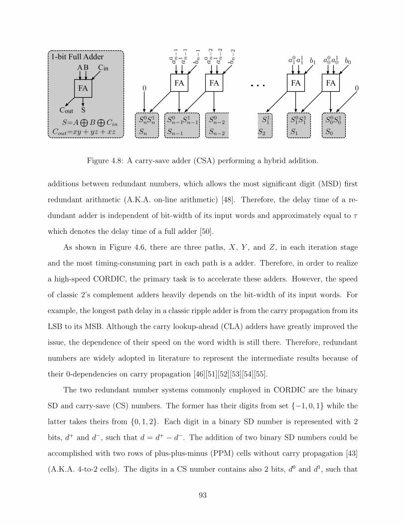
FA
AB
S
Cin
Cout
1-bit Full Adder
FAFAFAFA
Figure 4.8: A carry-save adder (CSA) performing a hybrid addition.
additions between redundant numbers, which allows the most significant digit (MSD) first
redundant arithmetic (A.K.A. on-line arithmetic) [48]. Therefore, the delay time of a re-
dundant adder is independent of bit-width of its input words and approximately equal to τ
which denotes the delay time of a full adder [50].
As shown in Figure 4.6, there are three paths, X, Y , and Z, in each iteration stage
and the most timing-consuming part in each path is a adder. Therefore, in order to realize
a high-speed CORDIC, the primary task is to accelerate these adders. However, the speed
of classic 2’s complement adders heavily depends on the bit-width of its input words. For
example, the longest path delay in a classic ripple adder is from the carry propagation from its
LSB to its MSB. Although the carry lookup-ahead (CLA) adders have greatly improved the
issue, the dependence of their speed on the word width is still there. Therefore, redundant
numbers are widely adopted in literature to represent the intermediate results because of
their 0-dependencies on carry propagation [46][51][52][53][54][55].
The two redundant number systems commonly employed in CORDIC are the binary
SD and carry-save (CS) numbers. The former has their digits from set {−1, 0, 1} while the
latter takes theirs from {0, 1, 2}. Each digit in a binary SD number is represented with 2
bits, d+ and d−, such that d = d+ − d−. The addition of two binary SD numbers could be
accomplished with two rows of plus-plus-minus (PPM) cells without carry propagation [43]
(A.K.A. 4-to-2 cells). The digits in a CS number contains also 2 bits, d0 and d1, such that
93
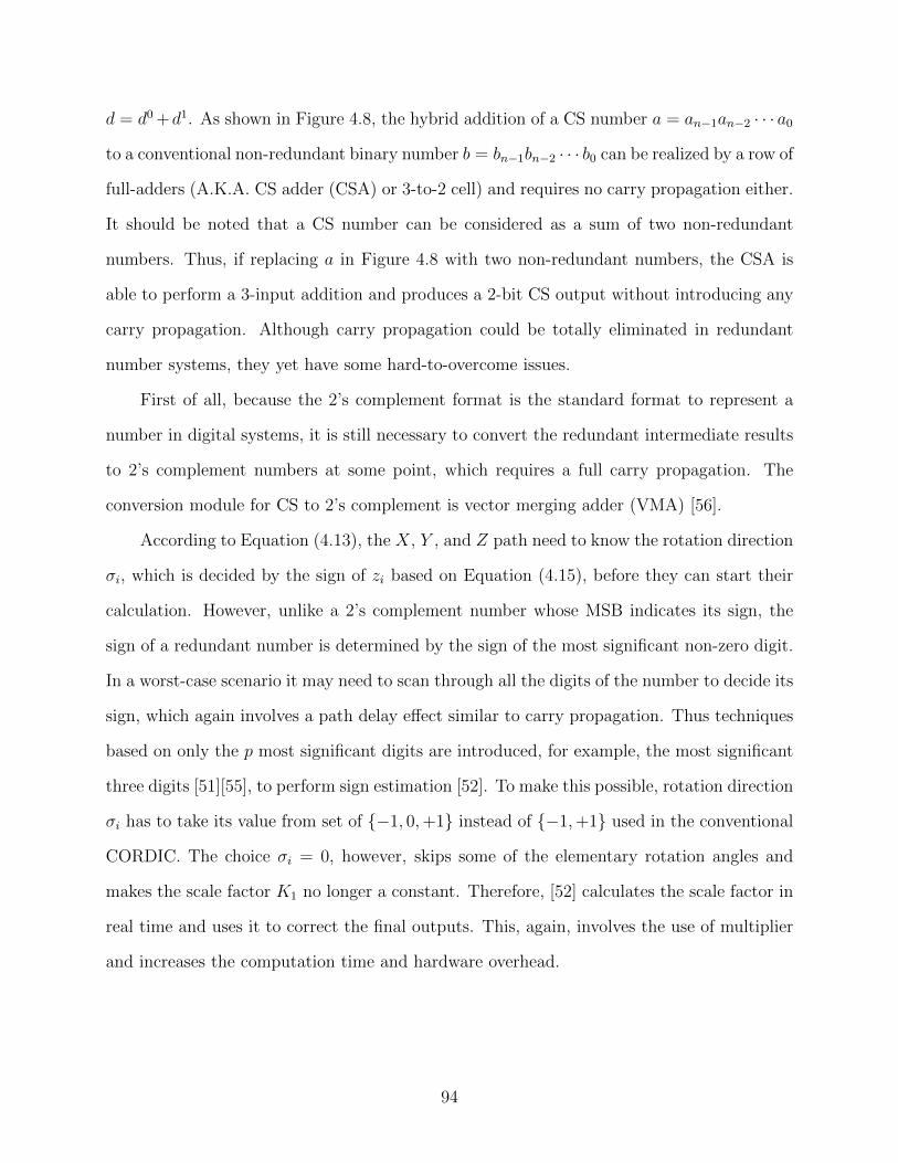
d = d0 +d1. As shown in Figure 4.8, the hybrid addition of a CS number a = an−1an−2 · · · a0
to a conventional non-redundant binary number b = bn−1bn−2 · · · b0 can be realized by a row of
full-adders (A.K.A. CS adder (CSA) or 3-to-2 cell) and requires no carry propagation either.
It should be noted that a CS number can be considered as a sum of two non-redundant
numbers. Thus, if replacing a in Figure 4.8 with two non-redundant numbers, the CSA is
able to perform a 3-input addition and produces a 2-bit CS output without introducing any
carry propagation. Although carry propagation could be totally eliminated in redundant
number systems, they yet have some hard-to-overcome issues.
First of all, because the 2’s complement format is the standard format to represent a
number in digital systems, it is still necessary to convert the redundant intermediate results
to 2’s complement numbers at some point, which requires a full carry propagation. The
conversion module for CS to 2’s complement is vector merging adder (VMA) [56].
According to Equation (4.13), the X, Y , and Z path need to know the rotation direction
σi, which is decided by the sign of zi based on Equation (4.15), before they can start their
calculation. However, unlike a 2’s complement number whose MSB indicates its sign, the
sign of a redundant number is determined by the sign of the most significant non-zero digit.
In a worst-case scenario it may need to scan through all the digits of the number to decide its
sign, which again involves a path delay effect similar to carry propagation. Thus techniques
based on only the p most significant digits are introduced, for example, the most significant
three digits [51][55], to perform sign estimation [52]. To make this possible, rotation direction
σi has to take its value from set of {−1, 0,+1} instead of {−1,+1} used in the conventional
CORDIC. The choice σi = 0, however, skips some of the elementary rotation angles and
makes the scale factor K1 no longer a constant. Therefore, [52] calculates the scale factor in
real time and uses it to correct the final outputs. This, again, involves the use of multiplier
and increases the computation time and hardware overhead.
94
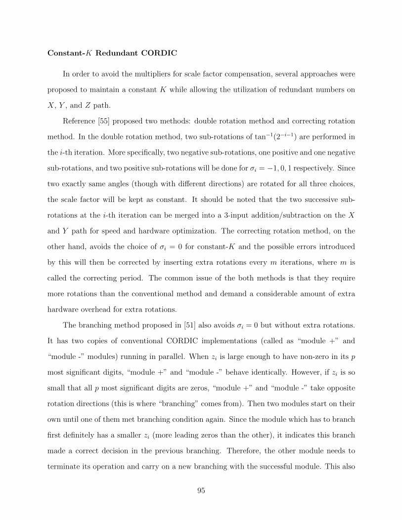
Constant-K Redundant CORDIC
In order to avoid the multipliers for scale factor compensation, several approaches were
proposed to maintain a constant K while allowing the utilization of redundant numbers on
X, Y , and Z path.
Reference [55] proposed two methods: double rotation method and correcting rotation
method. In the double rotation method, two sub-rotations of tan−1(2−i−1) are performed in
the i-th iteration. More specifically, two negative sub-rotations, one positive and one negative
sub-rotations, and two positive sub-rotations will be done for σi = −1, 0, 1 respectively. Since
two exactly same angles (though with different directions) are rotated for all three choices,
the scale factor will be kept as constant. It should be noted that the two successive sub-
rotations at the i-th iteration can be merged into a 3-input addition/subtraction on the X
and Y path for speed and hardware optimization. The correcting rotation method, on the
other hand, avoids the choice of σi = 0 for constant-K and the possible errors introduced
by this will then be corrected by inserting extra rotations every m iterations, where m is
called the correcting period. The common issue of the both methods is that they require
more rotations than the conventional method and demand a considerable amount of extra
hardware overhead for extra rotations.
The branching method proposed in [51] also avoids σi = 0 but without extra rotations.
It has two copies of conventional CORDIC implementations (called as “module +” and
“module -” modules) running in parallel. When zi is large enough to have non-zero in its p
most significant digits, “module +” and “module -” behave identically. However, if zi is so
small that all p most significant digits are zeros, “module +” and “module -” take opposite
rotation directions (this is where “branching” comes from). Then two modules start on their
own until one of them met branching condition again. Since the module which has to branch
first definitely has a smaller zi (more leading zeros than the other), it indicates this branch
made a correct decision in the previous branching. Therefore, the other module needs to
terminate its operation and carry on a new branching with the successful module. This also
95
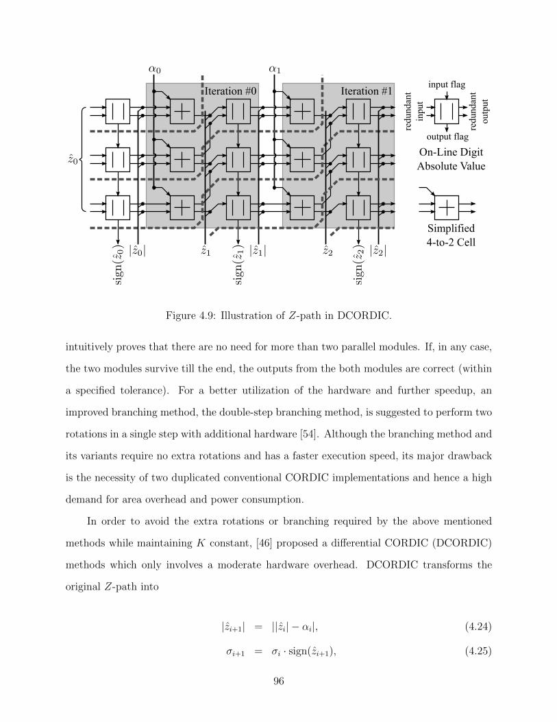
Iteration #0 Iteration #1
redu
ndan
t in
put
redu
ndan
t ou
tput
input flag
output flag
On-Line DigitAbsolute Value
Simplified 4-to-2 Cell
Figure 4.9: Illustration of Z-path in DCORDIC.
intuitively proves that there are no need for more than two parallel modules. If, in any case,
the two modules survive till the end, the outputs from the both modules are correct (within
a specified tolerance). For a better utilization of the hardware and further speedup, an
improved branching method, the double-step branching method, is suggested to perform two
rotations in a single step with additional hardware [54]. Although the branching method and
its variants require no extra rotations and has a faster execution speed, its major drawback
is the necessity of two duplicated conventional CORDIC implementations and hence a high
demand for area overhead and power consumption.
In order to avoid the extra rotations or branching required by the above mentioned
methods while maintaining K constant, [46] proposed a differential CORDIC (DCORDIC)
methods which only involves a moderate hardware overhead. DCORDIC transforms the
original Z-path into
|zi+1| = ||zi| − αi|, (4.24)
σi+1 = σi · sign(zi+1), (4.25)
96
In order to calculate the absolute value of a redundant number, it is necessary to scan the
number digit-by-digit from the MSD to find the 1st non-zero digit and use it to decide the sign
of the number. Once the sign is determined, the rest of the digits will be left untouched if the
number is positive or flipped to their reverse polarities if negative. Figure 4.9 demonstrates
the basic idea of how DCORDIC parallelizes the operations in Equation (4.24) and (4.25).
In each iteration, zi is calculated first and its absolute value and sign are obtained in a
MSD-first style. In order to accelerate this serial operation, a bit-level pipelining technique
is employed to shorten the delay to a virtual 0. The thick gray dash lines in the figure
indicate the advance of the pipeline stages from left top to right bottom. Therefore, Z path
is able to supply the X and Y paths {σi} at a rather high speed. The major drawback of
the approach is that a number of initial pipeline delays need to be inserted at the beginning
of the X and Y paths to compensate for the delay between the sign(z0) and z0, which is
determined by the bit-width of z0. Thus this approach will cause larger hardware overhead
and longer pipeline latency than the conventional approach.
Shortening of Iteration Stages
The conventional CORDIC usually requires a considerable number of iterations to
achieve a specified accuracy. Thus there are also efforts in literatures dedicated to reduce
this number for high speed implementation.
Radix-r number systems, where r = 2x |x=2,3,4,···, are suggested in [57][58][59] for im-
plementing CORDIC. In high radix CORDICs, the elementary rotation angle αi in the i-th
iteration becomes tan−1(σir−i), where σi could be any one in the sets {−r/2, · · · , 0, · · · , r/2}.
It is obvious that each iteration has more choice for αi and this halves the total number of
iterations because of the speeding-up of the convergence. According to [59], r = 4 is the
only practical choice because σi is not integer power of 2 and complexity of each iteration
increase significantly if r > 4. However, because αi is not a fixed value any longer like in the
97
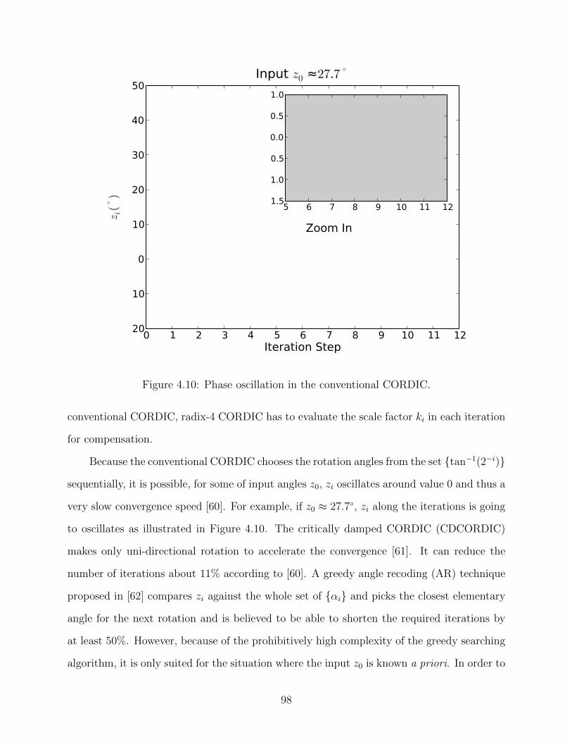
0 1 2 3 4 5 6 7 8 9 10 11 12Iteration Step
20
10
0
10
20
30
40
50
z i(
◦)
Zoom In
Input z0 ≈27.7◦
5 6 7 8 9 10 11 121.5
1.0
0.5
0.0
0.5
1.0
Figure 4.10: Phase oscillation in the conventional CORDIC.
conventional CORDIC, radix-4 CORDIC has to evaluate the scale factor ki in each iteration
for compensation.
Because the conventional CORDIC chooses the rotation angles from the set {tan−1(2−i)}
sequentially, it is possible, for some of input angles z0, zi oscillates around value 0 and thus a
very slow convergence speed [60]. For example, if z0 ≈ 27.7◦, zi along the iterations is going
to oscillates as illustrated in Figure 4.10. The critically damped CORDIC (CDCORDIC)
makes only uni-directional rotation to accelerate the convergence [61]. It can reduce the
number of iterations about 11% according to [60]. A greedy angle recoding (AR) technique
proposed in [62] compares zi against the whole set of {αi} and picks the closest elementary
angle for the next rotation and is believed to be able to shorten the required iterations by
at least 50%. However, because of the prohibitively high complexity of the greedy searching
algorithm, it is only suited for the situation where the input z0 is known a priori. In order to
98
improve the situation, a parallel angle recoding (PAR) technique was developed in [63][60].
Because z0 in a nearby region tend to choose a same series of αi, the PAR technique conducts
a range comparison, before the X and Y path starts their operation, to find out the optimum
series of αi and σi in one step. However, as the word length increases, the complexity of the
comparison logic increases drastically. Furthermore, all these three techniques skip angles in
{αi} to shorten iterations and thus have the well-known variable-K issue.
Range Utilization for K-compensation
The scaling factor ki introduced by each iteration stage, given in Equation (4.16), could
be also expressed using its Taylor series as
ki =√
1 + 2−2i = 1 +1
22−2i − 1
8
(2−2i
)2+
1
16
(2−2i
)3 − · · ·
= 1 + 2−2i−1 − 2−4i−3 + 2−8i−4 − · · · . (4.26)
Thus, according to [64][50], ki, for different i, could be approximated with different
approaches. More specifically, for N -bit fractional accuracy (which is 2−N if the truncation
is done by rounding), the approximation could be conducted according to the following
guidelines.
1. i ≥ dN−12e: All the 2nd and upper terms are smaller than 2−N and can be neglected,
so ki ≈ 1 and no K-compensation is required.
2. dN−34e ≤ i ≤ bN−1
2c: All the 3rd and upper terms are smaller than 2−N , so ki ≈
1− 2−2i−1 and K-compensation could be done by using one shift-and-add operation.
3. i ≤ bN−34c: No approximations and multiplier required for K-compensation.
A virtually K-free CORDIC was proposed in [65] by choosing αi only from those who
satisfy the 1st and 2nd conditions above. However, the eligible αi are so small that the
99
number of required iterations will be increased and hence more hardware cost be spent for
pipeline-style hardware implementation.
Parallelism on Z-path
The goal of the Z-path is to reconstruct z0 with a radix set {αi = tan−1(2−i) |i=0,1,2,···}
such thatn−1∑i=0
σi tan−1(2−i) → z0 (4.27)
and supply σi to X and Y path to proceed their calculation. In conventional CORDIC, this
reconstruction process is conducted in a sequential manner and involves addition/subtraction
operations. Thus Z-path becomes one of the bottlenecks for high-speed and area efficient
CORDIC designs [66].
A generalized formula was proposed in [67] to directly transform z0 to a rotation direction
vector {σi}, which makes a full parallelism on Z-path possible. However, the area of the
ROM it requires to store the precomputed values increases exponentially as the bit-with of
z0 increases [68].
Therefore, some techniques are proposed to directly tell σi from zi without involving
complicated mapping relationship. Before unveiling these approaches, a simple mathematical
derivation is conducted to build a relationship between function tan−1(2−i) and 2−i. The
Taylor series of a tan−1(2−i) is given by
tan−1(x) |x=2−i =∞∑i=0
(−1)n
2n+ 1x2n+1 |x=2−i
= 2−i − 1
3(2−i)3 +
1
5(2−i)5 − · · · (4.28)
and thus the difference between tan−1(2−i) and 2−i is
ε = 2−i − tan−1(2−i) =1
3(2−i)3 − 1
5(2−i)5 + · · · < 1
3(2−i)3. (4.29)
100
Therefor, if
1
32−3i ≤ 2M =⇒ i ≥
⌈M − log2 3
3
⌉, (4.30)
tan−1(2−i) is literally equal to 2−i within a M -bit fractional accuracy, 2−M . In other words, if
i is large enough, there is no difference to decompose zi with tan−1(2−i) or 2−i. Furthermore,
as a 2’s complement binary number, zi can be expressed as
zi = −bi2−i +Nz−1∑j=i+1
bj2−j, (4.31)
where bj |j≥i∈ {0, 1} and its index counts from the left-most bit in zi. According to [69][50],
zi has another equivalent expression
zi =Nz−1∑j=i+1
σj2−j − 2Nz−1, (4.32)
where σj ∈ {−1, 1} and can be easily calculated from bj−1 through
σj =
1− 2bj−1 j = i+ 1,
2bj−1 − 1 j = i+ 2, i+ 3, · · · .(4.33)
Therefore, from i-th iteration and beyond, where i satisfies Equation (4.30), zi can be ex-
pressed as
zi =Nz−1∑j=i+1
σj tan−1(2−j)− tan−1(2Nz−1). (4.34)
This Equation shows that zi could be decomposed with tan−1 function by using a very simple
conversion, given in Equation (4.33), if i ≥⌈Nz−log2 3
3
⌉. Because Equation (4.33) defines a
one-to-one mapping relationship, it can be implemented with simple and high-speed parallel
logic.
Unfortunately, this beautiful yet simple relationship does not work for a number of
iterations at the beginning, where i <⌈Nz−log2 3
3
⌉. [69] proposed to decompose tan−1(2−i)
101
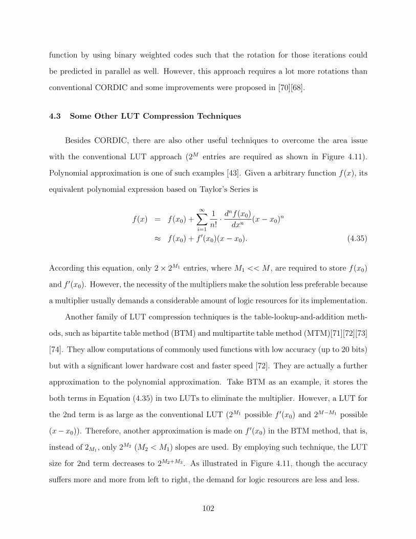
function by using binary weighted codes such that the rotation for those iterations could
be predicted in parallel as well. However, this approach requires a lot more rotations than
conventional CORDIC and some improvements were proposed in [70][68].
4.3 Some Other LUT Compression Techniques
Besides CORDIC, there are also other useful techniques to overcome the area issue
with the conventional LUT approach (2M entries are required as shown in Figure 4.11).
Polynomial approximation is one of such examples [43]. Given a arbitrary function f(x), its
equivalent polynomial expression based on Taylor’s Series is
f(x) = f(x0) +∞∑i=1
1
n!· d
nf(x0)
dxn(x− x0)n
≈ f(x0) + f ′(x0)(x− x0). (4.35)
According this equation, only 2× 2M1 entries, where M1 << M , are required to store f(x0)
and f ′(x0). However, the necessity of the multipliers make the solution less preferable because
a multiplier usually demands a considerable amount of logic resources for its implementation.
Another family of LUT compression techniques is the table-lookup-and-addition meth-
ods, such as bipartite table method (BTM) and multipartite table method (MTM)[71][72][73]
[74]. They allow computations of commonly used functions with low accuracy (up to 20 bits)
but with a significant lower hardware cost and faster speed [72]. They are actually a further
approximation to the polynomial approximation. Take BTM as an example, it stores the
both terms in Equation (4.35) in two LUTs to eliminate the multiplier. However, a LUT for
the 2nd term is as large as the conventional LUT (2M1 possible f ′(x0) and 2M−M1 possible
(x− x0)). Therefore, another approximation is made on f ′(x0) in the BTM method, that is,
instead of 2M1 , only 2M2 (M2 < M1) slopes are used. By employing such technique, the LUT
size for 2nd term decreases to 2M2+M3 . As illustrated in Figure 4.11, though the accuracy
suffers more and more from left to right, the demand for logic resources are less and less.
102
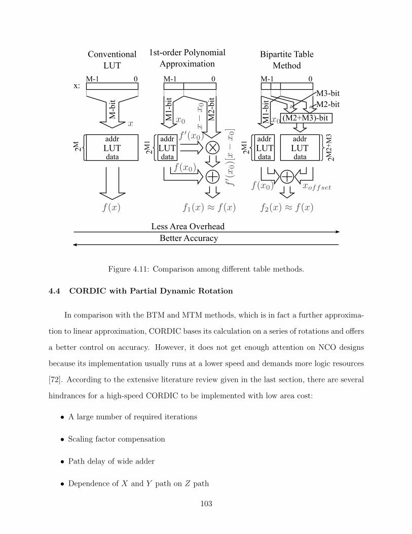
x:
ConventionalLUT
0
1st-order Polynomial Approximation
Bipartite Table Method
M-1
M-b
it
addr
dataLUT
0M-1
M1-
bit
M2-
bit
addr
dataLUT
0M-1
M1-
bit
addr
dataLUT
addr
dataLUT
M2-bitM3-bit
(M2+M3)-bit
2M 2M1
Less Area OverheadBetter Accuracy
2M1
2M2+
M3
Figure 4.11: Comparison among different table methods.
4.4 CORDIC with Partial Dynamic Rotation
In comparison with the BTM and MTM methods, which is in fact a further approxima-
tion to linear approximation, CORDIC bases its calculation on a series of rotations and offers
a better control on accuracy. However, it does not get enough attention on NCO designs
because its implementation usually runs at a lower speed and demands more logic resources
[72]. According to the extensive literature review given in the last section, there are several
hindrances for a high-speed CORDIC to be implemented with low area cost:
• A large number of required iterations
• Scaling factor compensation
• Path delay of wide adder
• Dependence of X and Y path on Z path
103
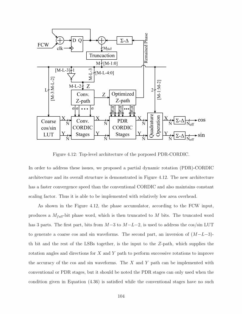
Coarsecos/sinLUT
Conv.CORDIC
Stages
PDRCORDIC
Stages
N
N
X
Y
N
N
X
Y
N
N
X
Y
Truncaction
Conv. Z-path
Optimized Z-path
Σ-Δ
σ σ,α
FCWclk
cos
sin
Z
Mfull
Z
[M-3
:M-L
-2]
Σ-Δ
Σ-Δ
D Q
[M-1:0]M
LM
-L-3 [M-L-4:0]
Neff
Neff
σ σ σ,α
σ,α
Rem
aine
d P
hase
Qua
drat
ure
Ope
rati
on[M
-1:M
-2]
2
N
N
X
Y
[M-L-3]
M-L-2
1
Figure 4.12: Top-level architecture of the porposed PDR-CORDIC.
In order to address these issues, we proposed a partial dynamic rotation (PDR)-CORDIC
architecture and its overall structure is demonstrated in Figure 4.12. The new architecture
has a faster convergence speed than the conventional CORDIC and also maintains constant
scaling factor. Thus it is able to be implemented with relatively low area overhead.
As shown in the Figure 4.12, the phase accumulator, according to the FCW input,
produces a Mfull-bit phase word, which is then truncated to M bits. The truncated word
has 3 parts. The first part, bits from M−3 to M−L−2, is used to address the cos/sin LUT
to generate a coarse cos and sin waveforms. The second part, an inversion of (M−L−3)-
th bit and the rest of the LSBs together, is the input to the Z-path, which supplies the
rotation angles and directions for X and Y path to perform successive rotations to improve
the accuracy of the cos and sin waveforms. The X and Y path can be implemented with
conventional or PDR stages, but it should be noted the PDR stages can only used when the
condition given in Equation (4.36) is satisfied while the conventional stages have no such
104

restriction. Also the Z-path for the PDR stages could be optimized by using the techniques
proposed in Section 4.4.4. The last part is the two MSBs of the M -bit truncated phase word
and indicates the quadrature of the phase word. Since the CORDIC works only for phase in
the 1st-quadrature, these two quadrature bits are used to translate the cos and sin in the 1st
quadrature into the four quadratures based on the symmetry among these four quadratures.
Σ-∆ noise shaping filters are also inserted to utilize some of valuable information which
would be thrown away otherwise. The proposed techniques utilized in the PDR-CORDIC
architecture will be further discussed in the following subsections.
4.4.1 Partial Dynamic Rotation
As discussed in Section 4.2.3, in order to accelerate the phase convergence in CORDIC,
the phase step taken by each rotation should be dynamically chosen from {αi}. However,
this process may skip some of phase step in {αi}, which causes a variable K. The extra
hardware required for dynamic selection and K compensation, such as barrel shifters and
multipliers, may not be able to be compensated even though the number of stages could be
greatly shortened.
However, if the following condition is satisfied (please also refer to 4.2.3),
i ≥⌈N − 1
2
⌉, (4.36)
the rotation angles are so small that no K-compensation is required. Thus, we proposed a
partial dynamic rotation (PDR) technique, which limits the dynamic rotation to the iteration
steps satisfied Equation (4.36), to make a faster convergence to reduce the number of required
rotations. A PDR stage could be implemented as shown in Figure 4.13. In comparison with
a conventional static stage given in Figure 4.6, the extra hardware cost for a PDR-stage
includes the dynamic rotation selection (DRS) logic and barrel shifters. The DRS logic finds
out the closest elementary rotation angle αj from the set {αi} and passes j to the barrel
105

-1
-1
Sig
nD
etec
tor
-1
>>j
>>j
01
01
0
1
D1
D2
D3
Q1
Q2
Q3
clk
DR
S
PDR Angle LUT
BarrelShifter
BarrelShifter
DynamicRotationSelection
Figure 4.13: Implementation of a partial dynamic rotation (PDR) stage.
shifter to perform programmable bit shift on the X and Y paths. Such overhead is usually far
less than the benefits which are achieved by decreasing the number of the required rotations
and can be easily compensated.
By utilizing the proposed PDR technique, the phase convergence speed can be greatly
accelerated. A simulation was conducted to study its effect on the convergence acceleration.
In the simulation, the same input z sequence was fed into two cascaded conventional stages
and PDR stages respectively. The remaining z coming out from these two 2-stage rotators
were recorded and plotted in Figure 4.14. From it, we can see that PDR not only has fast
convergence speed, but also a noise-like output for Z-path. In a NCO system, the remaining
phase combines with the truncated phase and present themselves as phase noise in the system
output. Furthermore, if the remaining phase is a highly-regulated periodic signal, it tends
to produce spurs in the output spectrum and degrade the SFDR performance. Since the
PDR technique produces noise-like Z-output, its phase noises are whiter, which means the
noise power is more likely to spread out at the output spectrum instead of concentrating at
106
500 1000 1500 2000 2500 3000 3500 4000time (# of clock cycles)
0.3
0.2
0.1
0.0
0.1
0.2
0.3re
main
ed
phase
(◦)
500 1000 1500 2000 2500 3000 3500 4000time (# of clock cycles)
0.08
0.06
0.04
0.02
0.00
0.02
0.04
0.06
0.08
rem
ain
ed
phase
(◦)
Figure 4.14: Phase convergence comparison between 2-stage static and PDR rotators.
one frequency and causing spurs. This natural dithering effect with the PDR technique is
another attractive feature for NCO design.
4.4.2 LUT for Range Reduction
According to the synthesis results given in section 4.1.2 and 4.2.2, we know that the
CORDIC outperforms LUT-based NCO only for large-N systems in term of area overhead.
When N is small, CORDIC demands even more area than LUT approach. Therefore, we
take advantage of such merit of the LUT method and incorporate it into the CORDIC to
achieve an area-optimized NCO design. As drawn in Figure 4.12, a cos/sin LUT is inserted
in front of a series of cascaded CORDIC rotation stages (which could be conventional or
107
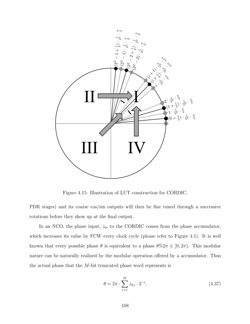
III
III IV
Figure 4.15: Illustration of LUT construction for CORDIC.
PDR stages) and its coarse cos/sin outputs will then be fine tuned through a successive
rotations before they show up at the final output.
In an NCO, the phase input, z0, to the CORDIC comes from the phase accumulator,
which increases its value by FCW every clock cycle (please refer to Figure 4.1). It is well
known that every possible phase θ is equivalent to a phase θ%2π ∈ [0, 2π). This modular
nature can be naturally realized by the modular operation offered by a accumulator. Thus
the actual phase that the M -bit truncated phase word represents is
θ = 2π ·M∑i=1
z0,i · 2−i, (4.37)
108
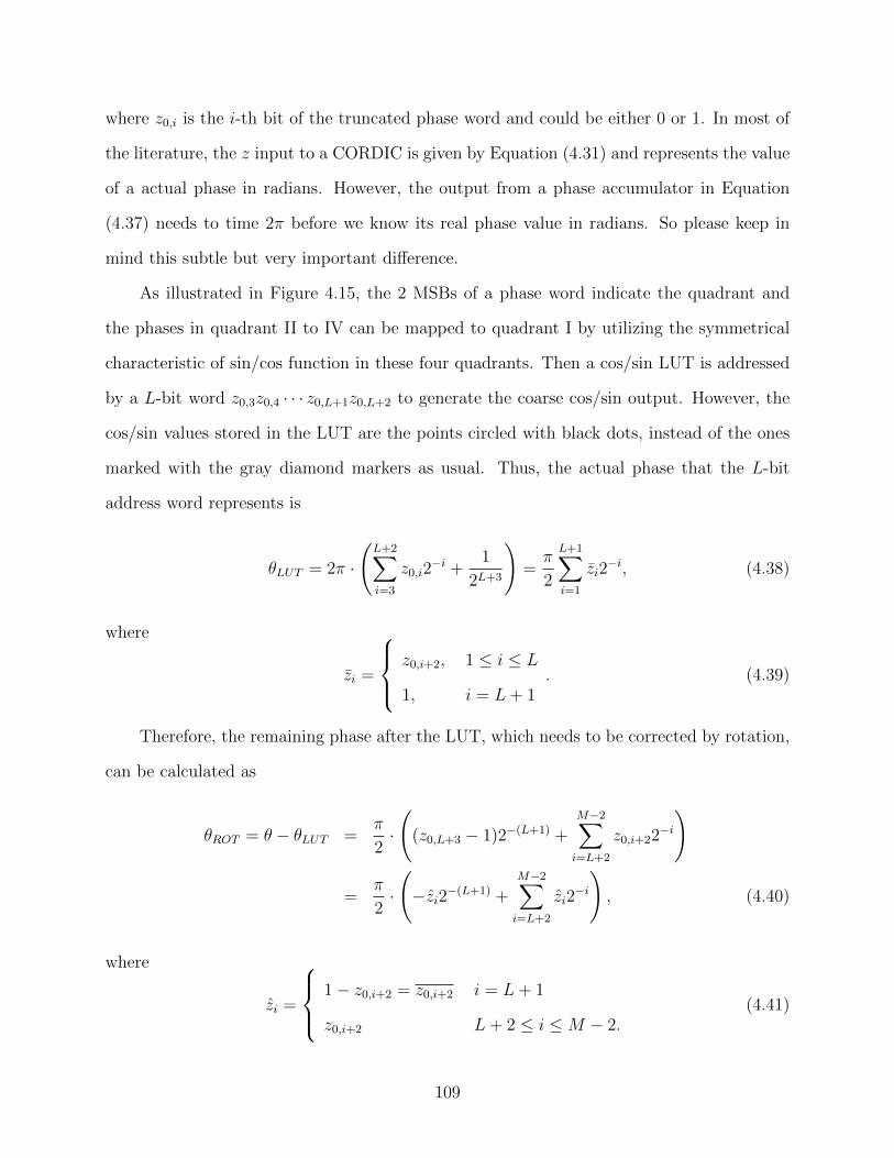
where z0,i is the i-th bit of the truncated phase word and could be either 0 or 1. In most of
the literature, the z input to a CORDIC is given by Equation (4.31) and represents the value
of a actual phase in radians. However, the output from a phase accumulator in Equation
(4.37) needs to time 2π before we know its real phase value in radians. So please keep in
mind this subtle but very important difference.
As illustrated in Figure 4.15, the 2 MSBs of a phase word indicate the quadrant and
the phases in quadrant II to IV can be mapped to quadrant I by utilizing the symmetrical
characteristic of sin/cos function in these four quadrants. Then a cos/sin LUT is addressed
by a L-bit word z0,3z0,4 · · · z0,L+1z0,L+2 to generate the coarse cos/sin output. However, the
cos/sin values stored in the LUT are the points circled with black dots, instead of the ones
marked with the gray diamond markers as usual. Thus, the actual phase that the L-bit
address word represents is
θLUT = 2π ·
(L+2∑i=3
z0,i2−i +
1
2L+3
)=π
2
L+1∑i=1
zi2−i, (4.38)
where
zi =
z0,i+2, 1 ≤ i ≤ L
1, i = L+ 1. (4.39)
Therefore, the remaining phase after the LUT, which needs to be corrected by rotation,
can be calculated as
θROT = θ − θLUT =π
2·
((z0,L+3 − 1)2−(L+1) +
M−2∑i=L+2
z0,i+22−i
)
=π
2·
(−zi2−(L+1) +
M−2∑i=L+2
zi2−i
), (4.40)
where
zi =
1− z0,i+2 = z0,i+2 i = L+ 1
z0,i+2 L+ 2 ≤ i ≤M − 2.(4.41)
109
Phase
Accum
ulator
FCW
clk
TruncationMfull M
2
LUT
[M-1:M
-2]
[M-1:0]
Quadrant
L
[M-3:M
-L-2]
1 [M-L-3]
M-L-3
[M-L-4:0]
[M-L-3:0]
Rotation
M-L-2
Figure 4.16: Separation of phase word for LUT and rotation.
It is obvious that zi ∈ {0, 1} and z0 = zL+1zL+2 · · · zM−3zM−2 represents a 2’s complement
number. z0 could be easily obtained by inverting the (L+ 3)-th bit of z0 and duplicating the
rest of the bits as illustrated in Figure 4.16.
If the LUT is constructed by using the points marked by the gray diamond markers
in Figure 4.15, the remaining phase would be in the range of [0, 12L· π
2). However, through
a simple manipulation of choosing the point circled with black dots, the range would be
[− 12L+1 · π2 ,
12L+1 · π2 ) instead. Compared to the former solution, the latter will decrease the
phase to be rotated by half and hence shorten the number of required rotations.
By introducing LUTs into CORDIC, not only can a number of initial rotations be
skipped for saving area overhead, but also the accuracy could be improved. According to
section 4.2.2, the quantization errors contributed by each stage are accumulated together.
Thus, the more rotations there are, the more the accuracy would suffer. Since the intro-
duction of LUTs tends to shorten the iterations, the accuracy would also be improved as
well.
4.4.3 X and Y Merging
The pipelined CORDIC design utilizes a great number of registers, which are inserted
between the stages to improve the system throughput. However, a register itself consumes a
considerable area compared with other gates, such as AND, OR, etc. Besides, a design with
a heavy utilization of registers usually requires a dedicated clock tree to distribute the clock
to every registers, which also introduces extra area overhead. Thus, one of the primary tasks
110
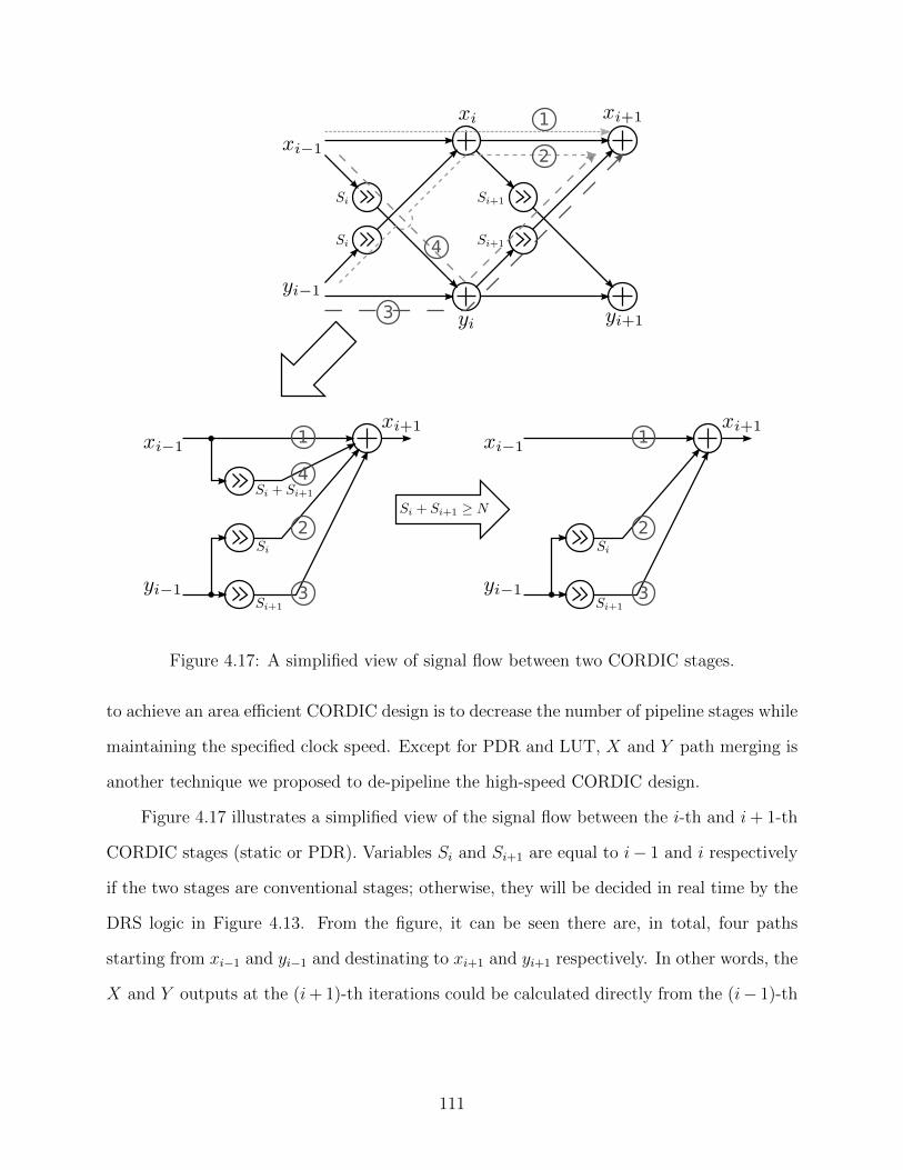
1
2
4
3
1
4
3
2
1
3
2
Figure 4.17: A simplified view of signal flow between two CORDIC stages.
to achieve an area efficient CORDIC design is to decrease the number of pipeline stages while
maintaining the specified clock speed. Except for PDR and LUT, X and Y path merging is
another technique we proposed to de-pipeline the high-speed CORDIC design.
Figure 4.17 illustrates a simplified view of the signal flow between the i-th and i+ 1-th
CORDIC stages (static or PDR). Variables Si and Si+1 are equal to i− 1 and i respectively
if the two stages are conventional stages; otherwise, they will be decided in real time by the
DRS logic in Figure 4.13. From the figure, it can be seen there are, in total, four paths
starting from xi−1 and yi−1 and destinating to xi+1 and yi+1 respectively. In other words, the
X and Y outputs at the (i+ 1)-th iterations could be calculated directly from the (i− 1)-th
111

iteration’s outputs through
xi+1 = xi−1 − σi2−Siyi−1 − σi+12−Si+1yi−1 − σiσi+12−Si−Si+1xi−1, (4.42a)
yi+1 = yi−1 + σi2−Sixi−1 + σi+12−Si+1xi−1 + σiσi+12−Si−Si+1yi−1. (4.42b)
It is known that the iteration step i has to satisfy Equation (4.36) for PDR stages. Further-
more, the i-th PDR stage picks its shift indexes from a set of {i− 1, i, i+ 1, · · · }. So
Si ≥ i− 1 and Si+1 ≥ i. (4.43)
Considering Equation (4.36) and (4.43) together, it is easy to see that
Si + Si+1 ≥ 2i− 1 ≥ 2 ·⌈N − 1
2
⌉− 1 ≥ N. (4.44)
Thus, the fourth terms in Equation (4.42) are equal to zero if N -bit is used for CORDIC’s
internal resolution and the equation could be rewritten as
xi+1 = xi−1 − σi2−Siyi−1 − σi+12−Si+1yi−1, (4.45a)
yi+1 = yi−1 + σi2−Sixi−1 + σi+12−Si+1xi−1. (4.45b)
This merging operation for PDR stages is also demonstrated in Figure 4.17. From it, we
can see that originally the X and Y path of two consecutive PDR stages needs four barrel
shifters and four 2-input adders all together. After such an merging manipulation, they
could be realized with four barrel shifters and two 3-input adders. Though such a change
looks like it is worthless because a 3-input 2’s complement addition still needs two traditional
adders, the introduction of CS arithmetic makes the 3-input addition a lot more attractive.
As discussed in Section 4.2.3, the CSA is able to perform such an addition by using a row
of full-adder without introducing carry propagation and produce a output in CS format.
112
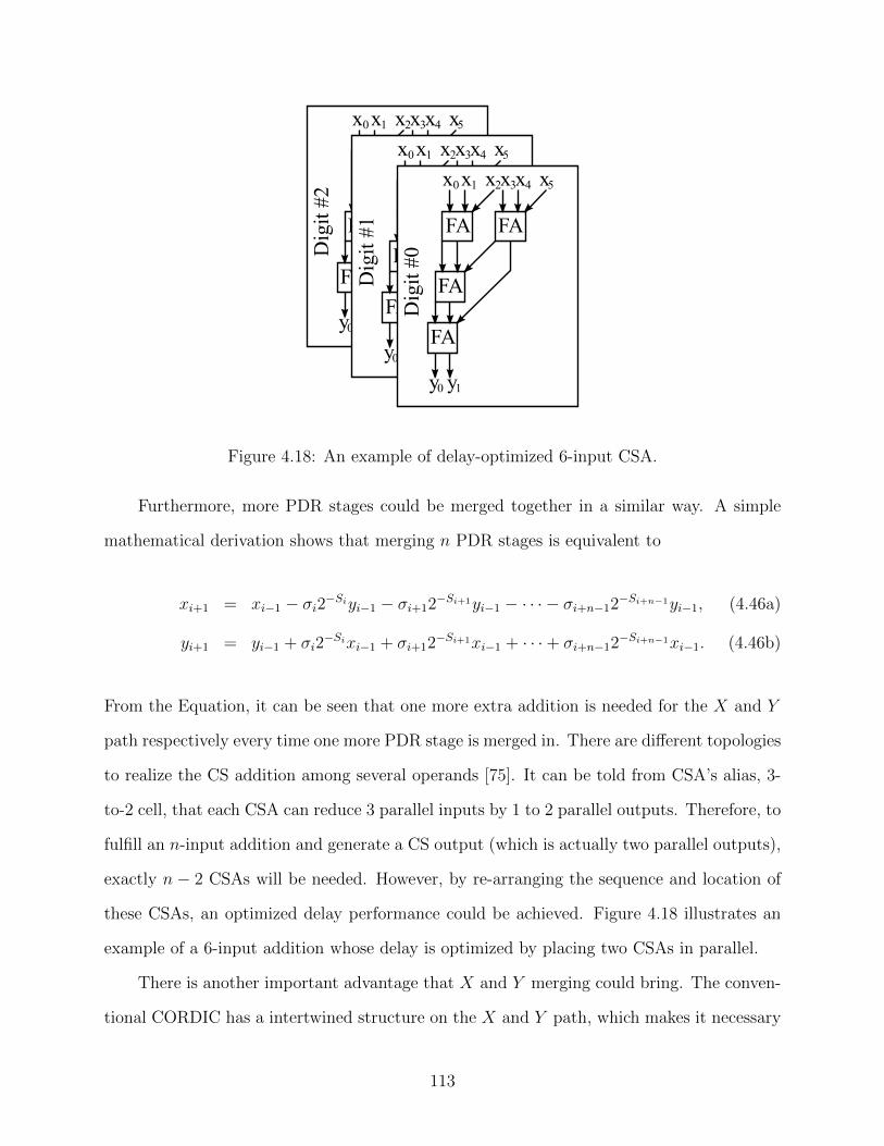
FA FA
FA
FA
x0 x1 x2x3x4 x5
y0 y1
Dig
it #
2 FA FA
FA
FA
x0 x1 x2x3x4 x5
y0 y1
Dig
it #
1 FA FA
FA
FA
x0 x1 x2x3x4 x5
y0 y1
Dig
it #
0
Figure 4.18: An example of delay-optimized 6-input CSA.
Furthermore, more PDR stages could be merged together in a similar way. A simple
mathematical derivation shows that merging n PDR stages is equivalent to
xi+1 = xi−1 − σi2−Siyi−1 − σi+12−Si+1yi−1 − · · · − σi+n−12−Si+n−1yi−1, (4.46a)
yi+1 = yi−1 + σi2−Sixi−1 + σi+12−Si+1xi−1 + · · ·+ σi+n−12−Si+n−1xi−1. (4.46b)
From the Equation, it can be seen that one more extra addition is needed for the X and Y
path respectively every time one more PDR stage is merged in. There are different topologies
to realize the CS addition among several operands [75]. It can be told from CSA’s alias, 3-
to-2 cell, that each CSA can reduce 3 parallel inputs by 1 to 2 parallel outputs. Therefore, to
fulfill an n-input addition and generate a CS output (which is actually two parallel outputs),
exactly n − 2 CSAs will be needed. However, by re-arranging the sequence and location of
these CSAs, an optimized delay performance could be achieved. Figure 4.18 illustrates an
example of a 6-input addition whose delay is optimized by placing two CSAs in parallel.
There is another important advantage that X and Y merging could bring. The conven-
tional CORDIC has a intertwined structure on the X and Y path, which makes it necessary
113

indexi
αi =tan−1(2−i+1)
binary codeof αi
2π
Ideal Boundarybetween αi and αi+1
Approximated Boundarybetween αi and αi+1
6 ≈ 1.7899◦ 01010001 00111100 01000000
7 ≈ 0.8951◦ 00101000 00011110 00100000
8 ≈ 0.4476◦ 00010100 00001111 00010000
9 ≈ 0.2238◦ 00001010 00000111 00001000
10 ≈ 0.1119◦ 00000101 N/A N/A
Table 4.4: Possible {αi} for PDR stages for N = 12 and M = 14.
to calculate the X and Y together at the same time. But usually only one output is needed
from NCO, either cos or sin, in a typical application of DDS. So the hardware dedicated to
quadrature output in CORDIC is wasted to a certain degree. However, by merging the X
and Y path, the dependence of X and Y on each other in PDR stages is eliminated as given
in Equation (4.46). Thus, if only one output is required from CORDIC, only the calculation
on X or Y will be involved and the demand for barrel shifters and adders will be cut by half.
4.4.4 Optimization on Z-path
When several PDR stages are merged together, multiple σi need to be supplied at
the same time as suggested by Equation (4.46). This raises the necessity of parallelizing
the Z-path. There are basically three approaches to realize the parallelism of Z-path: 1)
conventional cascaded adders; 2) range comparison method; 3) angle recoding. The first two
of them are suited for the situation when there are only 2-3 PDR stages. However, if there
are more PDR stages involved, the last approach should be considered.
The first approach is based on the original concept of the conventional CORDIC algo-
rithm. Because zi already becomes small when it arrives at the PDR stages, the bit-width on
Z-path at these iterations is much narrower than that of initial iterations. It is much easier
to implement the high-speed adders with narrow bit-width. Therefore, when there are only a
114
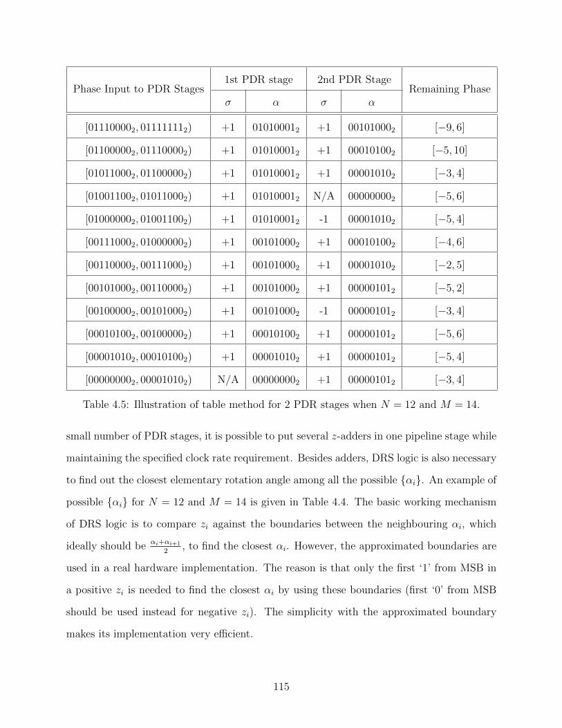
Phase Input to PDR Stages1st PDR stage 2nd PDR Stage
Remaining Phaseσ α σ α
[011100002, 011111112) +1 010100012 +1 001010002 [−9, 6]
[011000002, 011100002) +1 010100012 +1 000101002 [−5, 10]
[010110002, 011000002) +1 010100012 +1 000010102 [−3, 4]
[010011002, 010110002) +1 010100012 N/A 000000002 [−5, 6]
[010000002, 010011002) +1 010100012 -1 000010102 [−5, 4]
[001110002, 010000002) +1 001010002 +1 000101002 [−4, 6]
[001100002, 001110002) +1 001010002 +1 000010102 [−2, 5]
[001010002, 001100002) +1 001010002 +1 000001012 [−5, 2]
[001000002, 001010002) +1 001010002 -1 000001012 [−3, 4]
[000101002, 001000002) +1 000101002 +1 000001012 [−5, 6]
[000010102, 000101002) +1 000010102 +1 000001012 [−5, 4]
[000000002, 000010102) N/A 000000002 +1 000001012 [−3, 4]
Table 4.5: Illustration of table method for 2 PDR stages when N = 12 and M = 14.
small number of PDR stages, it is possible to put several z-adders in one pipeline stage while
maintaining the specified clock rate requirement. Besides adders, DRS logic is also necessary
to find out the closest elementary rotation angle among all the possible {αi}. An example of
possible {αi} for N = 12 and M = 14 is given in Table 4.4. The basic working mechanism
of DRS logic is to compare zi against the boundaries between the neighbouring αi, which
ideally should be αi+αi+1
2, to find the closest αi. However, the approximated boundaries are
used in a real hardware implementation. The reason is that only the first ‘1’ from MSB in
a positive zi is needed to find the closest αi by using these boundaries (first ‘0’ from MSB
should be used instead for negative zi). The simplicity with the approximated boundary
makes its implementation very efficient.
115

The second approach, the range comparison method, performs a range comparison on
zi to find out a combination of αi, which would give a minimum phase remainder. Table 4.5
illustrates an example of a range comparison method applied on Z-path for 2 PDR stages
while N = 12 and M = 14. It should be noted that only the positive input is listed in
the table for simplicity. The negative input could be processed in a similar way after a | · |
operation except the rotation directions are opposite. According to the range at which the
z input are located, rotation direction and angle, σ and α, for all PDR stages are decided in
parallel instead of one pair at one time as in the first approach. It can be observed that the
offsets between the different ranges in Table 4.5 are not even. The reason is that the listed
ranges have been manually adjusted already for simpler combinational logic design.
It is not difficult to notice that the first two approaches are sort of brutal-force methods
and only suited for applications with 2-3 PDR stages. Beyond this number, the complexity of
the both methods would grow too fast to have an implementation with reasonable hardware
cost.
The third approach is a analytical method. As discussed in Section 4.2.3, each digit of zi
could be used directly to indicate the pair of σ and α according to Equation (4.33) for most of
CORDIC designs in literatures if i satisfies Equation (4.30). There are two obstacles for such
technique to be employed in CORDIC for NCO designs. First, the binary representation of
z needs to multiply by 2π before it can use this technique; Second, the PDR stages take the
elementary rotation angle from {αi} dynamically rather than sequentially as in conventional
stages.
Because 2π = 6.2831853 · · ·10 = 0110.01001 · · ·2, the multiplication of z to 2π could be
approximated by
z = z × 2π ≈ (z << 2) + (z << 1) + (z >> 2). (4.47)
Thus three shifters and a 3-input addition are required for the approximation and they can
be realized by hard-wired connection and a CSA-VMA pair respectively. More shifters and
operands for addition will be needed if more accuracy is desired.
116
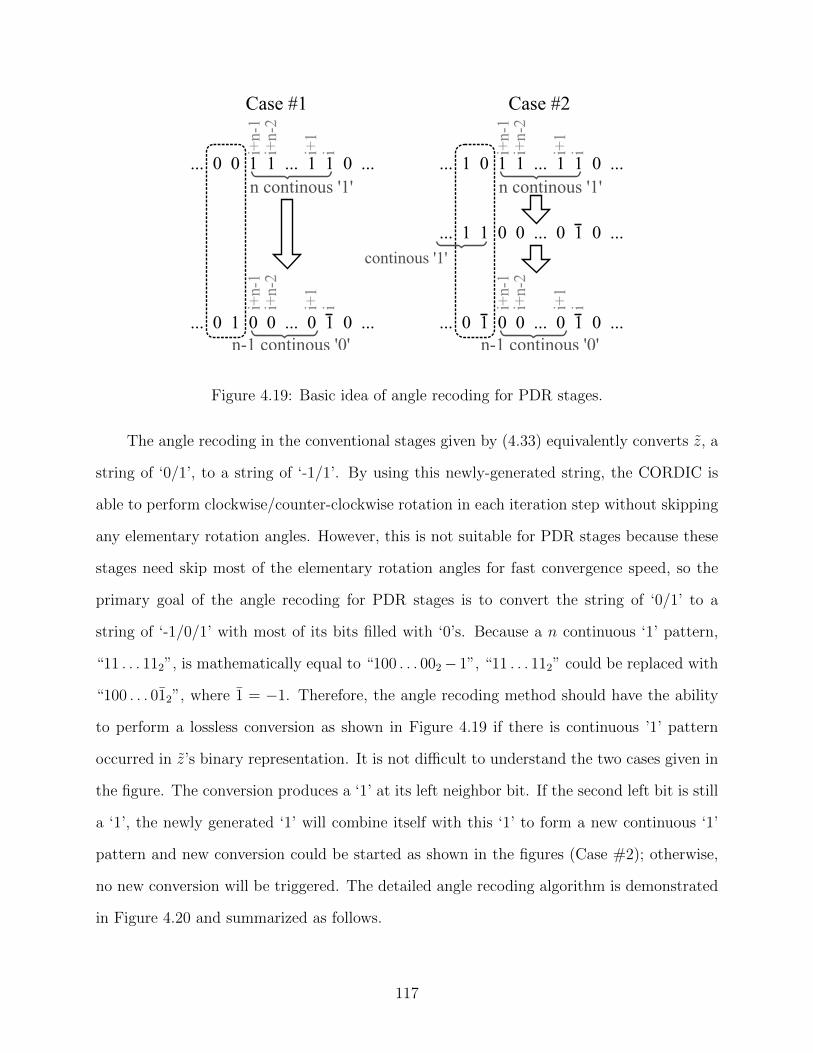
... 0 0 1 1 ... 1 1 0 ...n continous '1'
ii+1
i+n-
1i+
n-2
... 0 1 0 0 ... 0 1 0 ...n-1 continous '0'
Case #1 Case #2
continous '1'
ii+1
i+n-
1i+
n-2
... 1 0 1 1 ... 1 1 0 ...n continous '1'
... 1 1 0 0 ... 0 1 0 ...
... 0 1 0 0 ... 0 1 0 ...n-1 continous '0'
ii+1
i+n-
1i+
n-2
ii+1
i+n-
1i+
n-2
Figure 4.19: Basic idea of angle recoding for PDR stages.
The angle recoding in the conventional stages given by (4.33) equivalently converts z, a
string of ‘0/1’, to a string of ‘-1/1’. By using this newly-generated string, the CORDIC is
able to perform clockwise/counter-clockwise rotation in each iteration step without skipping
any elementary rotation angles. However, this is not suitable for PDR stages because these
stages need skip most of the elementary rotation angles for fast convergence speed, so the
primary goal of the angle recoding for PDR stages is to convert the string of ‘0/1’ to a
string of ‘-1/0/1’ with most of its bits filled with ‘0’s. Because a n continuous ‘1’ pattern,
“11 . . . 112”, is mathematically equal to “100 . . . 002− 1”, “11 . . . 112” could be replaced with
“100 . . . 012”, where 1 = −1. Therefore, the angle recoding method should have the ability
to perform a lossless conversion as shown in Figure 4.19 if there is continuous ’1’ pattern
occurred in z’s binary representation. It is not difficult to understand the two cases given in
the figure. The conversion produces a ‘1’ at its left neighbor bit. If the second left bit is still
a ‘1’, the newly generated ‘1’ will combine itself with this ‘1’ to form a new continuous ‘1’
pattern and new conversion could be started as shown in the figures (Case #2); otherwise,
no new conversion will be triggered. The detailed angle recoding algorithm is demonstrated
in Figure 4.20 and summarized as follows.
117
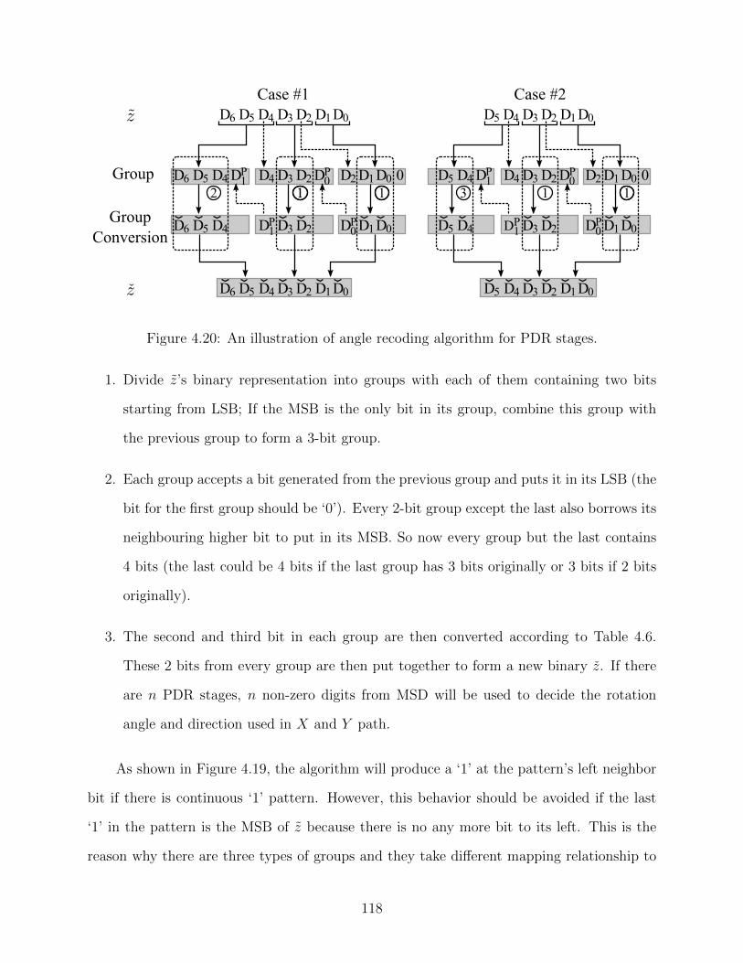
D4 D3 D2 D1 D0D6 D5
D4 D3 D2 D1 D0D6 D5 D2
D1 D0DP0
DP0D4
D3 D2DP1
DP1
D4D5
D1 D0D3 D2
D6
D4D5D6
Group
GroupConversion
D4 D3 D2 D1 D0D5
D4 D3 D2 D1 D0D5 D2
D1 D0DP0
DP0D4
D3 D2DP1
DP1
D4D5
D1 D0D3 D2D4D5
0 0
Case #1 Case #2
2 31 11 11
Figure 4.20: An illustration of angle recoding algorithm for PDR stages.
1. Divide z’s binary representation into groups with each of them containing two bits
starting from LSB; If the MSB is the only bit in its group, combine this group with
the previous group to form a 3-bit group.
2. Each group accepts a bit generated from the previous group and puts it in its LSB (the
bit for the first group should be ‘0’). Every 2-bit group except the last also borrows its
neighbouring higher bit to put in its MSB. So now every group but the last contains
4 bits (the last could be 4 bits if the last group has 3 bits originally or 3 bits if 2 bits
originally).
3. The second and third bit in each group are then converted according to Table 4.6.
These 2 bits from every group are then put together to form a new binary z. If there
are n PDR stages, n non-zero digits from MSD will be used to decide the rotation
angle and direction used in X and Y path.
As shown in Figure 4.19, the algorithm will produce a ‘1’ at the pattern’s left neighbor
bit if there is continuous ‘1’ pattern. However, this behavior should be avoided if the last
‘1’ in the pattern is the MSB of z because there is no any more bit to its left. This is the
reason why there are three types of groups and they take different mapping relationship to
118
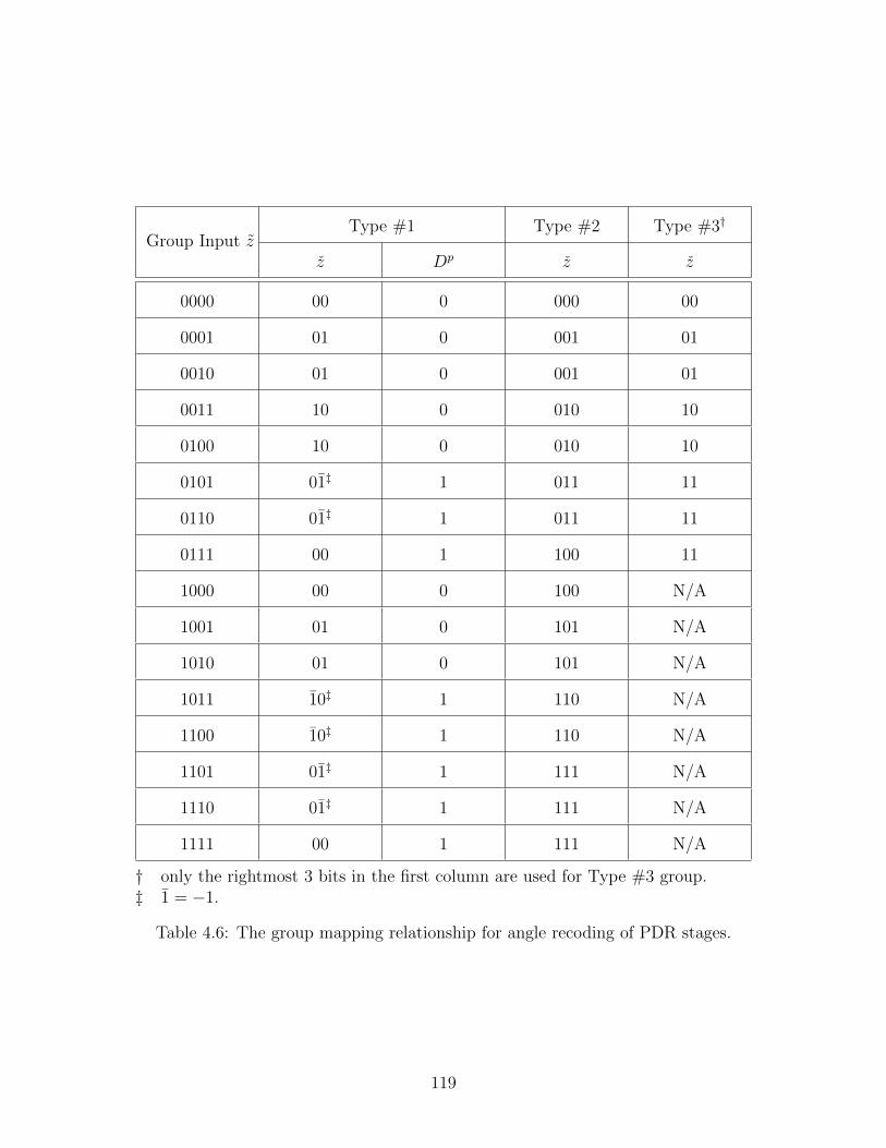
Group Input zType #1 Type #2 Type #3†
z Dp z z
0000 00 0 000 00
0001 01 0 001 01
0010 01 0 001 01
0011 10 0 010 10
0100 10 0 010 10
0101 01‡ 1 011 11
0110 01‡ 1 011 11
0111 00 1 100 11
1000 00 0 100 N/A
1001 01 0 101 N/A
1010 01 0 101 N/A
1011 10‡ 1 110 N/A
1100 10‡ 1 110 N/A
1101 01‡ 1 111 N/A
1110 01‡ 1 111 N/A
1111 00 1 111 N/A
† only the rightmost 3 bits in the first column are used for Type #3 group.‡ 1 = −1.
Table 4.6: The group mapping relationship for angle recoding of PDR stages.
119
perform the bit conversion. This is also the reason why the MSB could not be the only bit
in a group.
The three approaches have their own pros and cons, there is no guarantee which of
them is the best. The decision of which approach should be chosen depends on the context
of applications. Different approaches could be tried out to fit into the CORDIC and then
make the decision according to the area and power required for each of them at the specified
clock rate.
4.4.5 Σ-∆ Noise Shaping
It is not difficult to notice that, through a close observation to CORDIC, some of valuable
information is thrown away without gaining anything. First, we know that words wider than
Neff have to be used on X and Y path in order to achieve a effective number of bit Neff
and the extra bits at the LSB side are truncated at the final output to Neff . Second, the
remaining phase after a certain number of rotations is also abandoned for nothing. These
two forms of truncations occurred on the amplitude and phase represent a small value in
quantity. Given a signal before truncation x(t) and its truncated part has a value of e(t),
the signal after truncation, y(t), will be
y(t) = x(t)− e(t) = x(t) + n(t), (4.48)
where n(t) = −e(t) and represents the truncation noise. In most of applications, n(t) is
modeled as white noise and thus has a uniform power spectrum density. According to
Equation (4.48), n(t) mixes itself with x(t)’s own truncation noise and present in the final
output y(t). In order to utilize n(t) instead of just throwing it away, Σ-∆ filter is introduced.
It post processes n(t) and reshapes its spectrum such that the low-frequency noise spectrum
could be greatly attenuated. The price for such an improvement is the amplification of
the noise spectrum at the high-frequency end [38]. However, by moving the noise to high
120
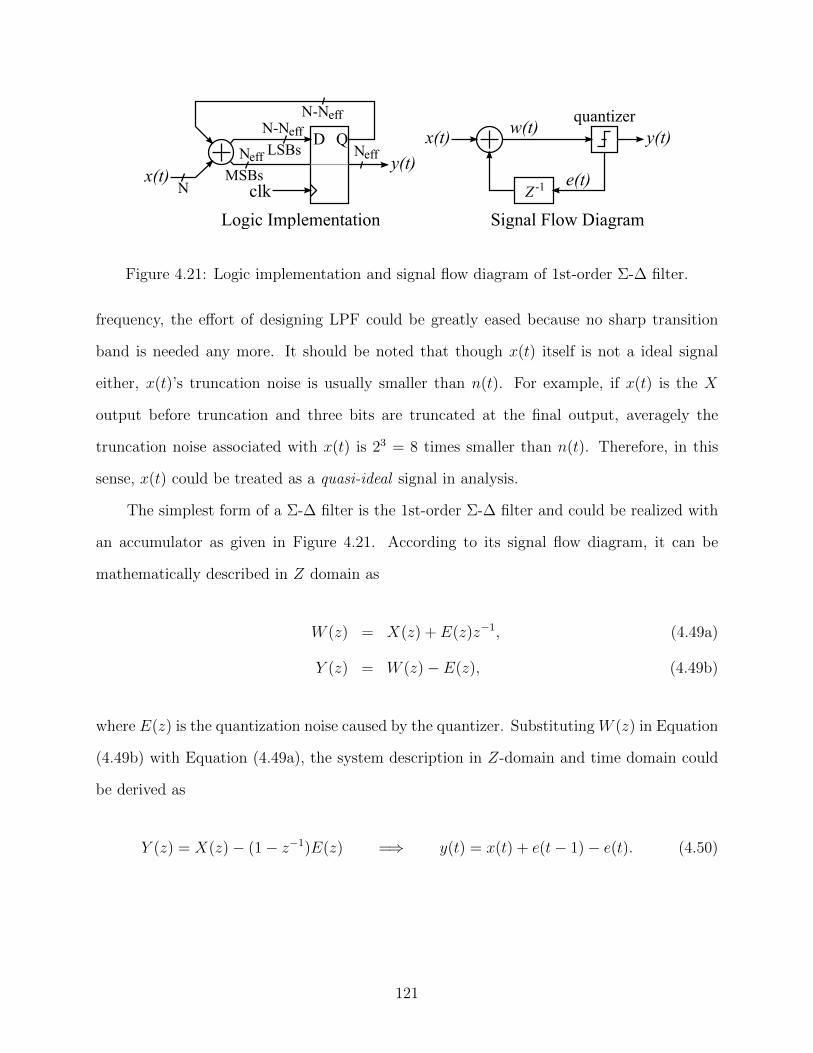
N
D Q
MSBsx(t)y(t)
Z -1
y(t)x(t)w(t)
e(t)
Logic Implementation Signal Flow Diagram
clk
N-Neff
Neff LSBs
quantizerN-Neff
Neff
Figure 4.21: Logic implementation and signal flow diagram of 1st-order Σ-∆ filter.
frequency, the effort of designing LPF could be greatly eased because no sharp transition
band is needed any more. It should be noted that though x(t) itself is not a ideal signal
either, x(t)’s truncation noise is usually smaller than n(t). For example, if x(t) is the X
output before truncation and three bits are truncated at the final output, averagely the
truncation noise associated with x(t) is 23 = 8 times smaller than n(t). Therefore, in this
sense, x(t) could be treated as a quasi-ideal signal in analysis.
The simplest form of a Σ-∆ filter is the 1st-order Σ-∆ filter and could be realized with
an accumulator as given in Figure 4.21. According to its signal flow diagram, it can be
mathematically described in Z domain as
W (z) = X(z) + E(z)z−1, (4.49a)
Y (z) = W (z)− E(z), (4.49b)
where E(z) is the quantization noise caused by the quantizer. Substituting W (z) in Equation
(4.49b) with Equation (4.49a), the system description in Z-domain and time domain could
be derived as
Y (z) = X(z)− (1− z−1)E(z) =⇒ y(t) = x(t) + e(t− 1)− e(t). (4.50)
121
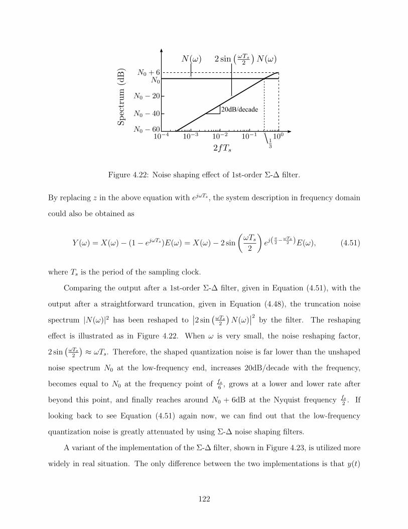
20dB/decade
Figure 4.22: Noise shaping effect of 1st-order Σ-∆ filter.
By replacing z in the above equation with ejωTs , the system description in frequency domain
could also be obtained as
Y (ω) = X(ω)− (1− ejωTs)E(ω) = X(ω)− 2 sin
(ωTs
2
)ej(
π2−ωTs
2 )E(ω), (4.51)
where Ts is the period of the sampling clock.
Comparing the output after a 1st-order Σ-∆ filter, given in Equation (4.51), with the
output after a straightforward truncation, given in Equation (4.48), the truncation noise
spectrum |N(ω)|2 has been reshaped to∣∣2 sin
(ωTs
2
)N(ω)
∣∣2 by the filter. The reshaping
effect is illustrated as in Figure 4.22. When ω is very small, the noise reshaping factor,
2 sin(ωTs
2
)≈ ωTs. Therefore, the shaped quantization noise is far lower than the unshaped
noise spectrum N0 at the low-frequency end, increases 20dB/decade with the frequency,
becomes equal to N0 at the frequency point of fs6
, grows at a lower and lower rate after
beyond this point, and finally reaches around N0 + 6dB at the Nyquist frequency fs2
. If
looking back to see Equation (4.51) again now, we can find out that the low-frequency
quantization noise is greatly attenuated by using Σ-∆ noise shaping filters.
A variant of the implementation of the Σ-∆ filter, shown in Figure 4.23, is utilized more
widely in real situation. The only difference between the two implementations is that y(t)
122
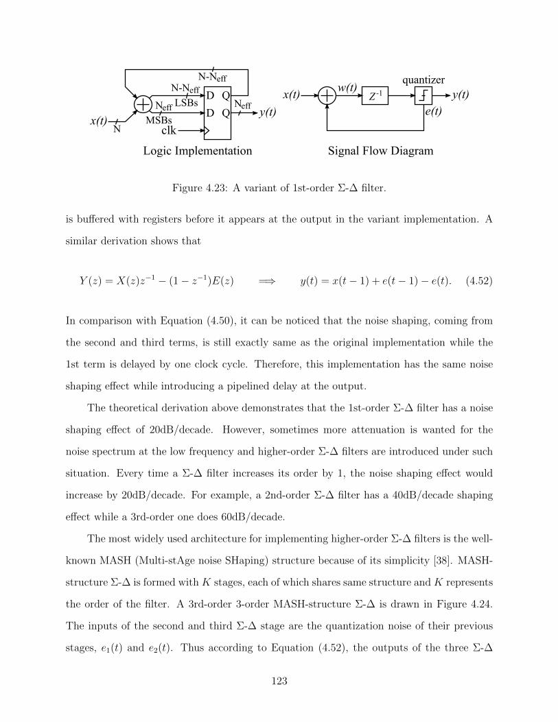
x(t)
Z -1 y(t)x(t)w(t)
e(t)
Logic Implementation Signal Flow Diagram
clk
quantizerN-Neff
MSBs
Neff LSBs
N-Neff
y(t)Neff
N
D Q
D Q
Figure 4.23: A variant of 1st-order Σ-∆ filter.
is buffered with registers before it appears at the output in the variant implementation. A
similar derivation shows that
Y (z) = X(z)z−1 − (1− z−1)E(z) =⇒ y(t) = x(t− 1) + e(t− 1)− e(t). (4.52)
In comparison with Equation (4.50), it can be noticed that the noise shaping, coming from
the second and third terms, is still exactly same as the original implementation while the
1st term is delayed by one clock cycle. Therefore, this implementation has the same noise
shaping effect while introducing a pipelined delay at the output.
The theoretical derivation above demonstrates that the 1st-order Σ-∆ filter has a noise
shaping effect of 20dB/decade. However, sometimes more attenuation is wanted for the
noise spectrum at the low frequency and higher-order Σ-∆ filters are introduced under such
situation. Every time a Σ-∆ filter increases its order by 1, the noise shaping effect would
increase by 20dB/decade. For example, a 2nd-order Σ-∆ filter has a 40dB/decade shaping
effect while a 3rd-order one does 60dB/decade.
The most widely used architecture for implementing higher-order Σ-∆ filters is the well-
known MASH (Multi-stAge noise SHaping) structure because of its simplicity [38]. MASH-
structure Σ-∆ is formed with K stages, each of which shares same structure and K represents
the order of the filter. A 3rd-order 3-order MASH-structure Σ-∆ is drawn in Figure 4.24.
The inputs of the second and third Σ-∆ stage are the quantization noise of their previous
stages, e1(t) and e2(t). Thus according to Equation (4.52), the outputs of the three Σ-∆
123
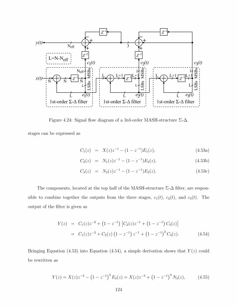
Z -1
y(t)
x(t)N N
LM
SB
s
Neff
N
LS
Bs
Z -1L+1
L
MS
Bs
1
LS
Bs
L=N-Neff
L L+1Z -1L+1 M
SB
s
1
LS
Bs
L L+1
L L L
1st-order Σ-Δ filter 1st-order Σ-Δ filter 1st-order Σ-Δ filter
L
Z -1
Z -1Z -2
Z -1
3
c (t)1 c (t)2 c (t)3
e (t)1 e (t)2 e (t)3
Neff
Figure 4.24: Signal flow diagram of a 3rd-order MASH-structure Σ-∆.
stages can be expressed as
C1(z) = X(z)z−1 − (1− z−1)E1(z), (4.53a)
C2(z) = N1(z)z−1 − (1− z−1)E2(z), (4.53b)
C3(z) = N2(z)z−1 − (1− z−1)E3(z). (4.53c)
The components, located at the top half of the MASH-structure Σ-∆ filter, are respon-
sible to combine together the outputs from the three stages, c1(t), c2(t), and c3(t). The
output of the filter is given as
Y (z) = C1(z)z−2 +(1− z−1
) [C2(z)z−1 +
(1− z−1
)C3(z)
]= C1(z)z−2 + C2(z)
(1− z−1
)z−1 +
(1− z−1
)2C3(z). (4.54)
Bringing Equation (4.53) into Equation (4.54), a simple derivation shows that Y (z) could
be rewritten as
Y (z) = X(z)z−3 −(1− z−1
)3E3(z) = X(z)z−3 +
(1− z−1
)3N3(z), (4.55)
124
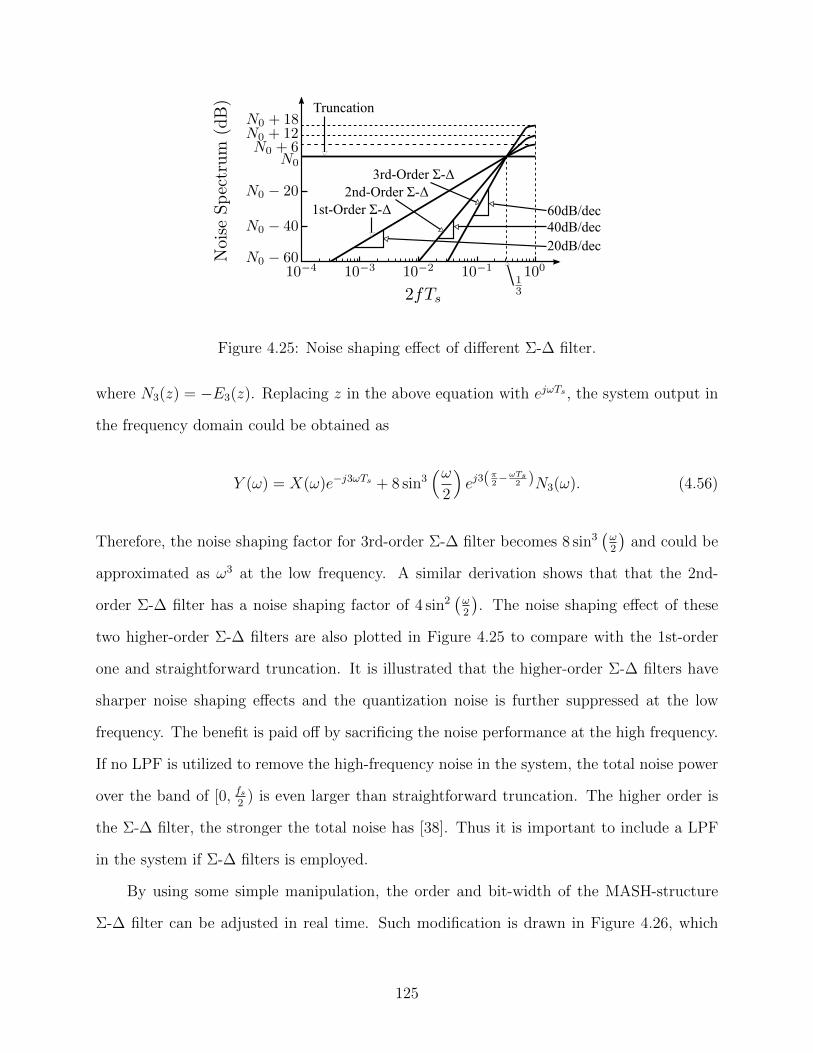
20dB/dec
Truncation
1st-Order Σ-Δ2nd-Order Σ-Δ
3rd-Order Σ-Δ
40dB/dec60dB/dec
Figure 4.25: Noise shaping effect of different Σ-∆ filter.
where N3(z) = −E3(z). Replacing z in the above equation with ejωTs , the system output in
the frequency domain could be obtained as
Y (ω) = X(ω)e−j3ωTs + 8 sin3(ω
2
)ej3(
π2−ωTs
2 )N3(ω). (4.56)
Therefore, the noise shaping factor for 3rd-order Σ-∆ filter becomes 8 sin3(ω2
)and could be
approximated as ω3 at the low frequency. A similar derivation shows that that the 2nd-
order Σ-∆ filter has a noise shaping factor of 4 sin2(ω2
). The noise shaping effect of these
two higher-order Σ-∆ filters are also plotted in Figure 4.25 to compare with the 1st-order
one and straightforward truncation. It is illustrated that the higher-order Σ-∆ filters have
sharper noise shaping effects and the quantization noise is further suppressed at the low
frequency. The benefit is paid off by sacrificing the noise performance at the high frequency.
If no LPF is utilized to remove the high-frequency noise in the system, the total noise power
over the band of [0, fs2
) is even larger than straightforward truncation. The higher order is
the Σ-∆ filter, the stronger the total noise has [38]. Thus it is important to include a LPF
in the system if Σ-∆ filters is employed.
By using some simple manipulation, the order and bit-width of the MASH-structure
Σ-∆ filter can be adjusted in real time. Such modification is drawn in Figure 4.26, which
125
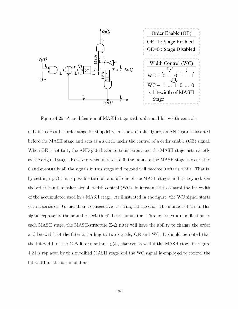
Z -1w(t)
L L+1L
MS
Bs
L
L+1
LS
Bs
L
c (t)2
e (t)2
e (t)1
OE
LWC
LL
L
L
L OE=1 : Stage Enabled
OE=0 : Stage Disabled
WC = 0 ... 0 1 ... 1
Order Enable (OE)
Width Control (WC)iL-i
i: bit-width of MASH Stage
WC = 1 ... 1 0 ... 0
Figure 4.26: A modification of MASH stage with order and bit-width controls.
only includes a 1st-order stage for simplicity. As shown in the figure, an AND gate is inserted
before the MASH stage and acts as a switch under the control of a order enable (OE) signal.
When OE is set to 1, the AND gate becomes transparent and the MASH stage acts exactly
as the original stage. However, when it is set to 0, the input to the MASH stage is cleared to
0 and eventually all the signals in this stage and beyond will become 0 after a while. That is,
by setting up OE, it is possible turn on and off one of the MASH stages and its beyond. On
the other hand, another signal, width control (WC), is introduced to control the bit-width
of the accumulator used in a MASH stage. As illustrated in the figure, the WC signal starts
with a series of ’0’s and then a consecutive-’1’ string till the end. The number of ’1’s in this
signal represents the actual bit-width of the accumulator. Through such a modification to
each MASH stage, the MASH-structure Σ-∆ filter will have the ability to change the order
and bit-width of the filter according to two signals, OE and WC. It should be noted that
the bit-width of the Σ-∆ filter’s output, y(t), changes as well if the MASH stage in Figure
4.24 is replaced by this modified MASH stage and the WC signal is employed to control the
bit-width of the accumulators.
126
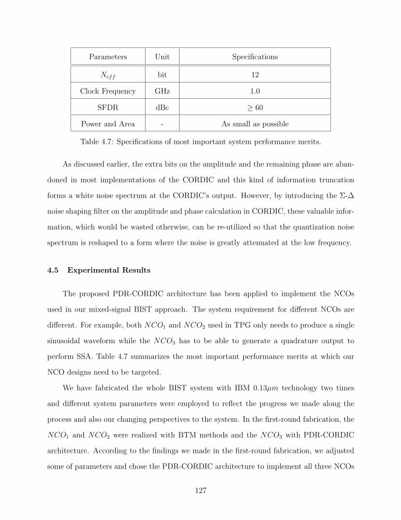
Parameters Unit Specifications
Neff bit 12
Clock Frequency GHz 1.0
SFDR dBc ≥ 60
Power and Area - As small as possible
Table 4.7: Specifications of most important system performance merits.
As discussed earlier, the extra bits on the amplitude and the remaining phase are aban-
doned in most implementations of the CORDIC and this kind of information truncation
forms a white noise spectrum at the CORDIC’s output. However, by introducing the Σ-∆
noise shaping filter on the amplitude and phase calculation in CORDIC, these valuable infor-
mation, which would be wasted otherwise, can be re-utilized so that the quantization noise
spectrum is reshaped to a form where the noise is greatly attenuated at the low frequency.
4.5 Experimental Results
The proposed PDR-CORDIC architecture has been applied to implement the NCOs
used in our mixed-signal BIST approach. The system requirement for different NCOs are
different. For example, both NCO1 and NCO2 used in TPG only needs to produce a single
sinusoidal waveform while the NCO3 has to be able to generate a quadrature output to
perform SSA. Table 4.7 summarizes the most important performance merits at which our
NCO designs need to be targeted.
We have fabricated the whole BIST system with IBM 0.13µm technology two times
and different system parameters were employed to reflect the progress we made along the
process and also our changing perspectives to the system. In the first-round fabrication, the
NCO1 and NCO2 were realized with BTM methods and the NCO3 with PDR-CORDIC
architecture. According to the findings we made in the first-round fabrication, we adjusted
some of parameters and chose the PDR-CORDIC architecture to implement all three NCOs
127
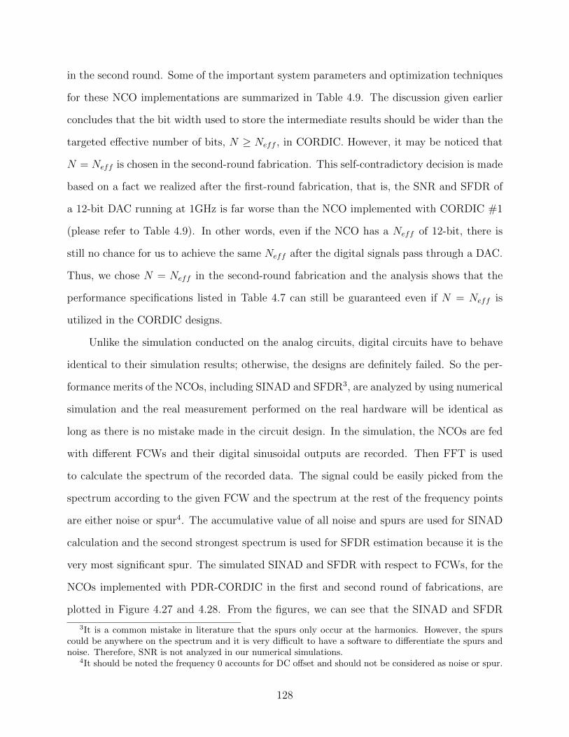
in the second round. Some of the important system parameters and optimization techniques
for these NCO implementations are summarized in Table 4.9. The discussion given earlier
concludes that the bit width used to store the intermediate results should be wider than the
targeted effective number of bits, N ≥ Neff , in CORDIC. However, it may be noticed that
N = Neff is chosen in the second-round fabrication. This self-contradictory decision is made
based on a fact we realized after the first-round fabrication, that is, the SNR and SFDR of
a 12-bit DAC running at 1GHz is far worse than the NCO implemented with CORDIC #1
(please refer to Table 4.9). In other words, even if the NCO has a Neff of 12-bit, there is
still no chance for us to achieve the same Neff after the digital signals pass through a DAC.
Thus, we chose N = Neff in the second-round fabrication and the analysis shows that the
performance specifications listed in Table 4.7 can still be guaranteed even if N = Neff is
utilized in the CORDIC designs.
Unlike the simulation conducted on the analog circuits, digital circuits have to behave
identical to their simulation results; otherwise, the designs are definitely failed. So the per-
formance merits of the NCOs, including SINAD and SFDR3, are analyzed by using numerical
simulation and the real measurement performed on the real hardware will be identical as
long as there is no mistake made in the circuit design. In the simulation, the NCOs are fed
with different FCWs and their digital sinusoidal outputs are recorded. Then FFT is used
to calculate the spectrum of the recorded data. The signal could be easily picked from the
spectrum according to the given FCW and the spectrum at the rest of the frequency points
are either noise or spur4. The accumulative value of all noise and spurs are used for SINAD
calculation and the second strongest spectrum is used for SFDR estimation because it is the
very most significant spur. The simulated SINAD and SFDR with respect to FCWs, for the
NCOs implemented with PDR-CORDIC in the first and second round of fabrications, are
plotted in Figure 4.27 and 4.28. From the figures, we can see that the SINAD and SFDR
3It is a common mistake in literature that the spurs only occur at the harmonics. However, the spurscould be anywhere on the spectrum and it is very difficult to have a software to differentiate the spurs andnoise. Therefore, SNR is not analyzed in our numerical simulations.
4It should be noted the frequency 0 accounts for DC offset and should not be considered as noise or spur.
128

Par
amet
ers
Tec
hniq
ues
N(b
it)
Neff
(bit
)M
full
(bit
)M (bit
)L
(bit
)H∗
K†
Σ-∆
onP
has
eΣ
-∆on
Am
plitu
de
Xan
dY
Mer
ging
Met
hod
ofZ
Opti
miz
atio
n
BT
M‡
-12
32-
--
--
--
-
CO
RD
IC#
1§15
1232
179
02
YY
Nca
scad
edad
der
CO
RD
IC#
2††
1212
2415
60
2Y
NY
range
com
par
ison
CO
RD
IC#
3‡‡
1212
2415
60
2N
NY
range
com
par
ison
∗H
:th
enum
ber
ofth
eco
nve
nti
onal
stag
es†
K:
the
num
ber
ofth
eP
DR
stag
es‡
NCO
1an
dNCO
2in
1st
fabri
cati
on.
§NCO
3in
1st
fabri
cati
on.
††NCO
1an
dNCO
2in
2nd
fabri
cati
on.
‡‡NCO
3in
2nd
fabri
cati
on.
Tab
le4.
8:Im
por
tant
syst
empar
amet
ers
and
tech
niq
ues
adop
ted
indiff
eren
tN
CO
imple
men
tati
ons.
129
1 1×216 2×216 3×216 4×216 5×216 6×216 7×216 8×216
FCW
73.0
73.5
74.0
74.5
75.0
SIN
AD
(dB
)
(a) SINAD vs. FCW
1 1×216 2×216 3×216 4×216 5×216 6×216 7×216 8×216
FCW
75
80
85
90
95
100
SFD
R (
dB
)
(b) SFDR vs. FCW
Figure 4.27: Noise performance of the CORDIC-based NCO in the 1st-round fabrication.
130

1 1×216 2×216 3×216 4×216 5×216 6×216 7×216 8×216
FCW
64
65
66
67
68
69
70
SIN
AD
(dB
)
(a) SINAD vs. FCW
1 1×216 2×216 3×216 4×216 5×216 6×216 7×216 8×216
FCW
60
65
70
75
80
85
SFD
R (
dB
)
(b) SFDR vs. FCW
Figure 4.28: Noise performance of the CORDIC-based NCO in the 2nd-round fabrication.
131
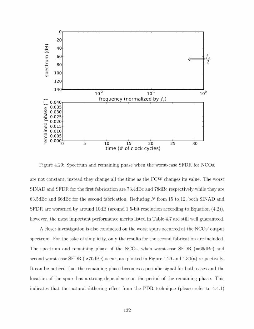
10-2 10-1100
frequency (normalized by fs )
140
120
100
80
60
40
20
0
spect
rum
(dB
)
0 5 10 15 20 25 30time (# of clock cycles)
0.0000.0050.0100.0150.0200.0250.0300.0350.040
rem
ain
ed p
hase
(◦)
Figure 4.29: Spectrum and remaining phase when the worst-case SFDR for NCOs.
are not constant; instead they change all the time as the FCW changes its value. The worst
SINAD and SFDR for the first fabrication are 73.4dBc and 78dBc respectively while they are
63.5dBc and 66dBc for the second fabrication. Reducing N from 15 to 12, both SINAD and
SFDR are worsened by around 10dB (around 1.5-bit resolution according to Equation (4.2)),
however, the most important performance merits listed in Table 4.7 are still well guaranteed.
A closer investigation is also conducted on the worst spurs occurred at the NCOs’ output
spectrum. For the sake of simplicity, only the results for the second fabrication are included.
The spectrum and remaining phase of the NCOs, when worst-case SFDR (=66dBc) and
second worst-case SFDR (≈70dBc) occur, are plotted in Figure 4.29 and 4.30(a) respectively.
It can be noticed that the remaining phase becomes a periodic signal for both cases and the
location of the spurs has a strong dependence on the period of the remaining phase. This
indicates that the natural dithering effect from the PDR technique (please refer to 4.4.1)
132
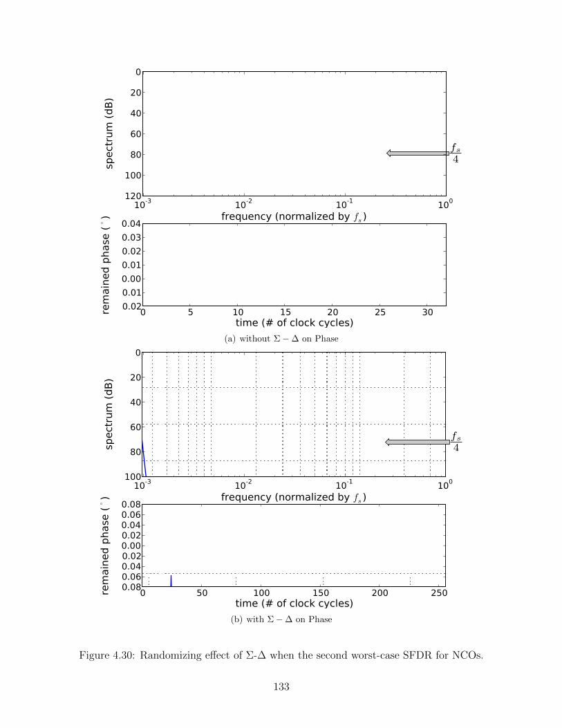
10-3 10-2 10-1100
frequency (normalized by fs )
120
100
80
60
40
20
0
spect
rum
(dB
)
0 5 10 15 20 25 30time (# of clock cycles)
0.02
0.01
0.00
0.01
0.02
0.03
0.04
rem
ain
ed p
hase
(◦)
(a) without Σ−∆ on Phase
10-3 10-2 10-1100
frequency (normalized by fs )
100
80
60
40
20
0
spect
rum
(dB
)
0 50 100 150 200 250time (# of clock cycles)
0.080.060.040.020.000.020.040.060.08
rem
ain
ed p
hase
(◦)
(b) with Σ−∆ on Phase
Figure 4.30: Randomizing effect of Σ-∆ when the second worst-case SFDR for NCOs.
133
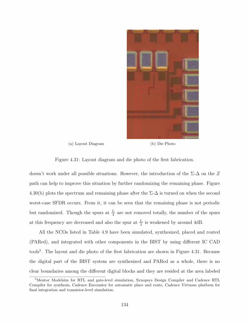
(a) Layout Diagram (b) Die Photo
Figure 4.31: Layout diagram and die photo of the first fabrication.
doesn’t work under all possible situations. However, the introduction of the Σ-∆ on the Z
path can help to improve this situation by further randomizing the remaining phase. Figure
4.30(b) plots the spectrum and remaining phase after the Σ-∆ is turned on when the second
worst-case SFDR occurs. From it, it can be seen that the remaining phase is not periodic
but randomized. Though the spurs at fs4
are not removed totally, the number of the spurs
at this frequency are decreased and also the spur at fs2
is weakened by around 4dB.
All the NCOs listed in Table 4.9 have been simulated, synthesized, placed and routed
(PARed), and integrated with other components in the BIST by using different IC CAD
tools5. The layout and die photo of the first fabrication are shown in Figure 4.31. Because
the digital part of the BIST system are synthesized and PARed as a whole, there is no
clear boundaries among the different digital blocks and they are resided at the area labeled
5Mentor Modelsim for RTL and gate-level simulation, Synopsys Design Compiler and Cadence RTLCompiler for synthesis, Cadence Encounter for automatic place and route, Cadence Virtuoso platform forfinal integration and transistor-level simulation.
134
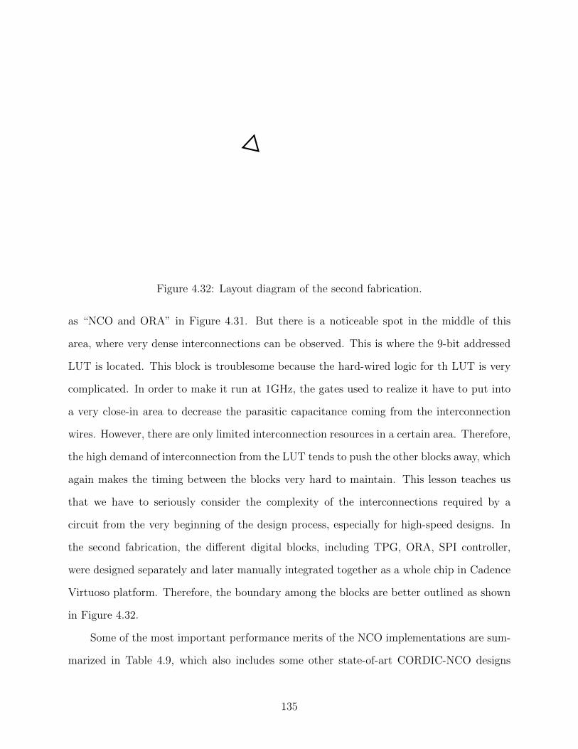
TPG DAC
ORA
SPI
Figure 4.32: Layout diagram of the second fabrication.
as “NCO and ORA” in Figure 4.31. But there is a noticeable spot in the middle of this
area, where very dense interconnections can be observed. This is where the 9-bit addressed
LUT is located. This block is troublesome because the hard-wired logic for th LUT is very
complicated. In order to make it run at 1GHz, the gates used to realize it have to put into
a very close-in area to decrease the parasitic capacitance coming from the interconnection
wires. However, there are only limited interconnection resources in a certain area. Therefore,
the high demand of interconnection from the LUT tends to push the other blocks away, which
again makes the timing between the blocks very hard to maintain. This lesson teaches us
that we have to seriously consider the complexity of the interconnections required by a
circuit from the very beginning of the design process, especially for high-speed designs. In
the second fabrication, the different digital blocks, including TPG, ORA, SPI controller,
were designed separately and later manually integrated together as a whole chip in Cadence
Virtuoso platform. Therefore, the boundary among the blocks are better outlined as shown
in Figure 4.32.
Some of the most important performance merits of the NCO implementations are sum-
marized in Table 4.9, which also includes some other state-of-art CORDIC-NCO designs
135

Pro
cess
(µm
)
Supply
Vol
tage
(V)
Mfull
(bit
)Neff
(bit
)W
orst
-Cas
eSF
DR
(dB
c)
Max
imum
Clo
ckF
req.
(Hz)
Synth
esis
Are
a∗
(mm
2)
Cor
eA
rea†
(mm
2)
Pow
er‡
(mW
/MH
z)
BT
M0.
131.
532
12N
/A90
0MN
/AN
/AN
/A
CO
RD
IC#
10.
131.
532
1278
900M
0.05
36N
/A0.
046
CO
RD
IC#
2§0.
131.
524
1266
1G0.
0301
0.03
850.
041
CO
RD
IC#
30.
131.
524
1266
1G0.
0111
N/A
0.01
5
Hybri
dC
OR
DIC
[76]
0.25
2.5
3213
9338
5MN
/A0.
220.
40
DC
OR
DIC
#1
[77]
0.13
1.2
1517
901G
0.35
N/A
0.35
DC
OR
DIC
#2
[77]
0.13
1.2
1210
601G
0.15
N/A
0.14
∗th
eov
eral
lar
eaof
the
gate
sin
the
synth
esiz
edga
te-l
evel
net
-lis
t.†
the
core
area
inth
efinal
chip
.‡
the
pow
erco
nsu
mpti
ons
list
edin
this
colu
mn
are
the
esti
mat
ions
rep
orte
dby
the
CA
Dto
ols
exce
pt
Hybri
dC
OR
DIC
,w
hos
ep
ower
isfr
omth
ere
alm
easu
rem
ent.
§C
OR
DIC
#2
conta
ins
two
CO
RD
IC,
two
Σ-∆
,an
dan
extr
aad
der
tofo
rma
two-
tone
DD
S.
Tab
le4.
9:Syst
emp
erfo
rman
ces
ofth
epro
pos
edC
OR
DIC
and
com
par
ison
wit
hst
ate-
of-a
rtdes
igns.
136
published in the literature. From such a comparison, a conclusion can be easily drawn that
the PDR-CORDIC architecture is highly efficient in terms of speed, area and power. For
example, the CORDIC #2 contains two CORDIC NCOs, two Σ-∆, and an extra adder, but
only takes up 0.0385mm2 silicon area. In fact, the area of one PDR-CORDIC NCO only
consumes around 38
of this area, 0.0144mm2. This is just about 6.5% of the area used by the
hybrid CORDIC [76], which however only runs at 40% of our speed and consumes nearly
27 times more power per MHz. Of course, the SFDR performance of our design is worse
than the hybrid CORDIC and DCORDIC #1. The reason lies in the fact that the other
two designs have wider outputs while we decrease the internal bit-width, N , on purpose to
save up the unnecessary power and area consumptions. In the application of DDS, a DAC
has to be inserted to transform the digital signal generated by the NCO to a analog signal.
However, the analog portion of the DAC is not ideal and there is rare cases that a DAC can
have a effective number of bits equal to its bit-width. Therefore, our design philosophy is
what we need is not perfect but just good enough.
137
Chapter 5
Conclusion
The proposed mixed-signal BIST architecture described in this dissertation utilizes the
SSA technique to perform the spectrum analysis on the DUT’s output such that some of
the very important spectrum-related characteristics of the DUT, such as frequency response,
linearity, noise, etc., can be estimated to compare against the specification. The SSA-based
ORA offers some unique advantages over the existed spectrum analysis techniques. First,
as a whole digital solution, the SSA does not have to tolerate the non-ideal effects of the
analog components and hence has better dynamic range and measurement accuracy than the
analog spectrum analysis techniques. Second, in comparison with the commonly used digital
spectrum analysis approach, the FFT, the SSA analyzes the spectrum at one frequency point
at one time and can be implemented with two sets of MACs and thus very efficient hardware.
Furthermore, the SSA also offers some flexibility that the FFT cannot provide. For example,
the maximum number of the points that an FFT processor can compute is fixed, such that
it is difficult, to adjust the frequency resolution when using an FFT-based ORA. Instead,
the frequency resolution can be easily tuned with the step size of the sweeping frequency in
SSA-based ORA and the number of samples used for accumulation. In addition, sometimes
we are only interested in several frequency points or in a narrow bandwidth, which can be
done easily using SSA-based ORA while FFT-based ORA has to compute a great amount
of useless information because FFT processes the whole frequency domain at one time.
It is intrinsic that the spectrum analysis has to shorten the signal under analysis in the
time domain with a timing window. Therefore, it is inevitable that the spectrum leakage
happens in the spectrum analysis and causes potential estimation errors. In order to reduce
the errors, the leakage has to be decreased by increasing the accumulation length. But the
138
attenuation rate of the side lobe of the spectrum of the rectangle window is so low that a long
test time is required to achieve a reasonable accuracy. Fortunately, in the proposed BIST
architecture, the DUT is driven by the TPG and thus the interested frequency is perfectly
synchronized with the reference frequency produced in the ORA if the TPG and ORA
operate under the same clock source. Because of this, it is possible to minimize the errors by
using IMP accumulation, which stops the accumulation at the IMPs of the frequency under
analysis. Since the IMP accumulation demands shorter test time, it also helps to decrease
the required bit width of the DC1 and DC2 accumulators to hold the test results and thus
reduce the area overhead. However, due to the discrete nature of a digital signal, not every
exact IMPs can be correctly predicted. Thus, the IMPs captured by the proposed IMP
circuits could be categorized as FIMPs and GIMPs and they are suited for different analog
measurements according to their advantages and drawbacks. The theoretical derivation and
simulation results prove the efficiency of the IMP circuits and accumulation in SSA-based
ORA.
In order to improve the dynamic range and measurement accuracy of the proposed BIST
architecture, high resolution DAC and ADC should be used. However, the area overhead
of the LUT-based NCO increases exponentially as the resolution of the converters increases.
The traditional LUT compression technique, table method, is an approximation of the Taylor
series. In order to achieve an efficient design, the table method has to employ heavy ap-
proximation and suffers poor SFDR and SINAD performance. In comparison, the CORDIC
algorithm approaches to the desired result through a series of vector rotations and its ac-
curacy is primarily determined by the number of rotations and the bit width to hold the
intermediate results. However, the conventional CORDIC requires a considerable number
of rotations to achieve a reasonable accuracy. So it is not as efficient as the table method
for high-resolution NCO design. It is proven that LUT is more efficient than CORDIC for
narrow phase input. Therefore, the proposed PDR-CORDIC algorithm starts with a sin/cos
LUT to get a coarse result such that a number of initial rotations can be skipped. Then
139
the coarse result is tuned to a finer result through a series of rotations. Fortunately, the
very last several rotations can be replaced with a half number of PDR rotations. Through
these approaches, the number of required rotations could be greatly reduced to a very lim-
ited number and a very efficient design is achieved. In addition, some other techniques,
such as the carry-save addition, xy-path flattening, Σ-∆ noise shaping, are also introduced
to improve the efficiency and performance of the PDR-CORDIC algorithm. The proposed
algorithm was simulated, verified, and fabricated with IBM 0.13µm BiCMOS technology.
The real measurement results confirm its superb efficiency and performance.
Overall, the proposed mixed-signal BIST architecture is a very promising candidate for
on-chip characterization tool for analog DUTs. Because most of the BIST resides in the
digital portion of the mixed-signal system, the system can be designed with parameterized
HDL model and easily migrated from one system to another. It also offers the system the
ability to characterize and calibrate itself on the fly such that the reliability of the overall
system could be improved and the maintenance costs be reduced.
In the future, it is promising to combine the quadrature CORDIC-based NCO and two
multipliers in the ORA together. When the CORDIC rotates a unit vector by a linearly
increasing phase, the CORDIC acts as a NCO and outputs a pair of digital sine and cosine
waveforms. However, if the vector rotated by the CORDIC has its x and y components
equal to the DUT’s output, y(t), and 0 respectively, the CORDIC will output y(t) · cosθ and
y(t) · sinθ. This is actually the operation completed by the NCO and the two multipliers in
the ORA. Therefore, by designing the CORDIC in this way, not only can the two multipliers
in the ORA be eliminated, but also the two accumulators and the CORDIC can be designed
together as a whole with the CSA optimization.
140
Bibliography
[1] L. T. Wang, C. Stroud, and N. Touba, System on Chip Test Architectures. MorganKaufmann, 2007.
[2] M. Bushnell and V. Agrawal, Essentials of Electronic Testing for Digital, Memory andMixed-Signal VLSI Circuits. Springer, 2000.
[3] H.-K. T. Ma, S. Devadas, A. Sangiovanni-Vincentelli, and R. Wei, “Logic verificationalgorithms and their parallel implementation,” IEEE Trans. on Computer-Aided Design,vol. 8, no. 2, pp. 181–189, 1999.
[4] C. Stroud, A Designer’s Guide to Built-In Self-Test. Springer, 2002.
[5] A. Hastings, The Art of Analog Layout, 2nd ed. Prentice Hall, 2005.
[6] A. Gopalan, “Built-in-self-test of RF front-end circuitry,” Ph.D. Dissertation, RochesterInstitute of Technology, 2005.
[7] G. Srinivasan, S. Bhattacharya, S. Cherubal, and A. Chatterjee, “Fast specification testof TDMA power amplifiers using transient current measurements,” IEE Proc. Comput-ers and Digital Techniques, vol. 152, no. 5, pp. 632–642, 2005.
[8] S. S. Akbay, A. Halder, A. Chatterjee, and D. Keezer, “Low-cost test of embeddedRF/analog mixed-signal circuits in SOPs,” IEEE Trans. on Advanced Packaging, vol. 27,no. 2, pp. 352–363, 2004.
[9] R. Voorakaranam and A. Chatterjee, “Test generation for accurate prediction of analogspecifications,” Proc. VLSI Test Symp., pp. 137–142, 2000.
[10] F. Dai, C. Stroud, and D. Yang, “Automatic linearity and frequency response tests withbuilt-in pattern generator and analyzer,” IEEE Trans. on VLSI Systems, vol. 14, no. 6,pp. 561–572, 2006.
[11] A. Halder, S. Bhattacharya, and A. Chatterjee, “Automatic multitone alternate testgeneration for RF circuits using behavioral models,” Proc. International Test Conf.,pp. 665–673, 2003.
[12] P. Variyam and A. Chatterjee, “Digital-compatible BIST for analog circuits using tran-sient response sampling,” IEEE Design and Test of Computer, vol. 17, no. 3, pp. 106–115, 2000.
141
[13] E. Acar and S. Ozev, “Go/No-Go testing of VCO modulation RF transceiver throughthe delayed-RF set-up,” IEEE Trans. on Very Large Scale Integration Systems, vol. 15,no. 1, pp. 37–47, 2007.
[14] F. Liu and S. Ozev, “Statistical test development for analog circuits under high processvariations,” IEEE Trans. on Computer-Aided Design of Integrated Circuits and Systems,vol. 26, no. 8, pp. 1465–1477, 2007.
[15] M. Sachdev and B. Atzema, “Industrial relevance of analog IFA: A fact or a fiction,”Proc. of IEEE International Test Conf., pp. 61–70, 1995.
[16] P. Variyam and et al., “Prediction of analog performance parameters using fast transienttesting,” IEEE Trans. on Computer-Aided Design of Integrated Circuits and Systems,vol. 21, no. 3, pp. 349–361, 2002.
[17] C. Stroud, J. Morton, A. Islam, and H. Alassaly, “A mixed-signal built-in self-testapproach for analog circuits,” Proc. IEEE Southwest Symp. on Mixed-Signal Design,pp. 196–201, 2003.
[18] V. Agrawal, R. Dauer, S. Jain, H. Kalvonjian, C. Lee, K. McGregor, M. Pahsan,C. Stroud, and L.-C. Suen, BIST at Your Fingertips Handbook. AT&T, 1987.
[19] J. B. Kim and S. H. Hong, “A CMOS built-in current sensor for IDDQ testing,” IEICETrans. Electronics, vol. E89-C, no. 6, pp. 868–870, 2006.
[20] J.-Y. Ryu, B. Kim, and I. Sylla, “A new low-cost RF built-in self-test measurementfor system-on-chip transceivers,” IEEE Trans. on Instrumentation and Measurement,vol. 55, no. 2, pp. 381–388, 2006.
[21] K. Arabi and B. Kaminska, “Efficient and accurate testing of analog-to-digital convertersusing oscillation-test method,” Proc. of Design and Test in Europe, pp. 348–352, 1997.
[22] B. Provost and E. Sanchez-Sinencio, “On-chip ramp generators for mixed-signal BISTand ADC self-test,” IEEE J. of Solid-State Circuits, vol. 38, no. 2, pp. 263–273, 2003.
[23] M. I. Products, “Application notes 283: INL/DNL measurments for high-speed analog-to-digital converters (ADCs),” 2000.
[24] H. W. Li, M. J. Dallabetta, and H. B. Demuth, “Measuring the impulse response oflinear systems using an analog correlator,” IEEE International Symp. on Circuits andSystems, vol. 5, pp. 65–68, 1994.
[25] C. Y. Pan and K. T. Cheng, “Pseudorandom testing for mixed-signal circuits,” IEEETrans. on Computer-Aided Design of Integrated Circuits and Systems, vol. 16, no. 10,pp. 1173–1185, 1997.
[26] A. Singh, C. Patel, and J. Plusquellic, “On-chip impulse response generation for analogand mixed-signal testing,” Proc. of International Test Conf., pp. 262–270, 2004.
142
[27] J. Emmert, J. Cheatham, B. Jagannathan, and S. Umarani, “An FFT approximationtechnique suitable for on-chip generation and analysis of sinusoidal signals,” Proc. ofIEEE International Symp. on Defect and Fault Tolerance in VLSI Systems, pp. 361–368,2003.
[28] A. Oppenheim and R. Schafer, Discrete-Time Signal Processing, 3rd ed. Prentice-Hall,2009.
[29] M. Mendez-Rivera, A. Valdes-Garcia, J. Silva-Martinez, and E. Sanchez-Sinencio, “Anon-chip spectrum analyzer for analog built-in testing,” J. of Electronic Testing: Theoryand Applications, vol. 21, no. 3, pp. 205–219, 2005.
[30] J. Park and et al., “A fully-integrated UHF receiver with multi-resolution spectrumsensing (MRSS) functionality for ieee 802.22 cognitive radio applications,” IEEE J. ofSolid-State Circuits, vol. 44, no. 1, pp. 258–268, 2005.
[31] A. Valdes-Garcia, W. Khalil, B. Bakkaloglu, J. Silva-Matinez, and E. Sanchez-Sinencio,“Built-in self test of RF transceiver SoCs: form signal chain to RF synthesizers,” IEEERadio Frequency Integrated Circuits Symp., pp. 335–338, 2007.
[32] J. Qin, C. Stroud, and F. Dai, “FPGA-based analog functional measurements for adap-tive control in mixed-signal systems,” IEEE Trans. on Industrial Electronics, vol. 54,no. 4, pp. 1885–1897, 2007.
[33] K. J. Astrom and B. Wittenmark, Adaptive Control, 2nd ed. Addison-Wesley, 1994.
[34] B. Razavi, RF Microelectronics. Prentice-Hall, 1997.
[35] J. Qin, C. Stroud, and F. Dai, “Phase delay measurement and calibration in built-inanalog functional testing,” Proc. of IEEE Southeastern Symp. on System Theory, pp.145–149, 2007.
[36] G. J. Starr, “Built-in self-test for the analysis of mixed-signal systems,” Master’s thesis,Auburn University, 2010.
[37] J. Qin, C. Stroud, and F. Dai, “Test time for multiplier accumulator based outputresponse analyzer in built-in analog functional testing,” Proc. of IEEE SoutheasternSymp. on System Theory, pp. 363–368, 2009.
[38] J. Rogers, C. Plett, and F. Dai, Integrated Circuit Design for High-Speed FrequencySynthesis. Artech House, 2006.
[39] Fast Fourier Transform v3.2, Xilinx Inc., 2005.
[40] J. Vankka, Digital Direct Synthesizers: Theory, Design and Applications. Springer,2001.
[41] J. E. Volder, “The CORDIC trigonometric computing technique,” IRE Trans. on Elec-tronic Computers, vol. EC-8, no. 3, pp. 330–334, 1959.
143
[42] J. S. Walther, “A unified algorithm for elementary functions,” Proc. of Spring JointComputer Conf., pp. 379–385, 1971.
[43] J.-M. Muller, Elementary Functions: Algorithms and Implementation, 2nd ed.Birkhauser, 2005.
[44] Y. H. Hu, “The quantization effects of the CORDIC algorithm,” IEEE Trans. on SignalProcessing, vol. 40, no. 4, pp. 834–844, 1992.
[45] D. D. Caro, N. Petra, and A. G. M. Strollo, “Digital synthesizer/mixer with hybridCORDIC-multiplier architecture: Error analysis and optimization,” IEEE Trans. onCircuit and Systems - I: Regular Papers, vol. 56, no. 2, pp. 364–373, 2009.
[46] H. Dawid and H. Meyr, “The differential CORDIC algorithm: Constant scale factorredundant implementation without correcting iterations,” IEEE Trans. on Computers,vol. 45, no. 3, pp. 307–318, 1996.
[47] K. Kota and J. R. Cavallaro, “Numberical accuracy and hardware tradeoffs for CORDICarithmetic for special-purpose processors,” IEEE Trans. on Computers, vol. 42, no. 7,pp. 769–779, 1993.
[48] K. K. Parhi, VLSI Digital Signal Processing Systems: Design and Implementation.John Wiley & Sons, 1999.
[49] A. Avizienis, “Signed-digit number presentations for fast parallel arithmetic,” IRETrans. on Electronic Computers, vol. EC-10, no. 3, pp. 389–400, 1961.
[50] D. Timmermann, H. Hahn, and B. J. Hosticka, “Low latency time CORDIC algorithms,”IEEE Trans. on Computer, vol. 41, no. 8, pp. 1010–1015, 1992.
[51] J. Duprat and J.-M. Muller, “The CORDIC algorithm: New results for fast VLSIimplementation,” IEEE Trans. on Computers, vol. 42, no. 2, pp. 168–178, 1993.
[52] M. D. Ercegovac and T. Lang, “Redundant and online CORDIC: Application to matrixtriangularization and svd,” IEEE Trans. on Computers, vol. 39, no. 6, pp. 725–740,1990.
[53] H. X. Lin and H. J. Sips, “On-line CORDIC algorithms,” IEEE Trans. on Computers,vol. 39, no. 8, pp. 1038–1052, 1990.
[54] D. S. Phatak, “Double step branching CORDIC: A new algorithm for fast sine andcosine generation,” IEEE Trans. on Computers, vol. 47, no. 5, pp. 587–602, 1998.
[55] N. Takagi, T. Asada, and S. Yajima, “Redundant CORDIC methods with a constantscale factor for sine and cosine computation,” IEEE Trans. on Computers, vol. 40, no. 9,pp. 989–995, 1991.
[56] T. G. Noll, “Carry-save architectures for high-speed digital signal processing,” J. ofVLSI Signal Processing, vol. 3, no. 1-2, pp. 121–140, 1991.
144
[57] E. Antelo, J. D. Bruguera, and E. L. Zapata, “Unified mixed radix 2-4 redundantCORDIC processor,” IEEE Trans. on Computers, vol. 45, no. 8, pp. 1068–1073, 1996.
[58] E. Antelo, J. Villalba, J. D. Bruguera, and E. L. Zapata, “High performance rotationarchitectures based on the radix-4 CORDIC algorithm,” IEEE Trans. on Computers,vol. 46, no. 8, pp. 855–870, 1997.
[59] J. D. Bruguera, E. Antelo, and E. L. Zapata, “Design of a pipelined radix-4 CORDICprocessor,” Elsevier J. Parallel Computing, vol. 19, no. 7, pp. 729–744, 1993.
[60] T. K. Rodrigues and E. E. Swartzlander, Jr., “Adaptive CORDIC: Using parallel an-gle recoding to accelerate rotations,” 40th Asilomar Conf. on Signals, Systems, andComputers, pp. 323–327, 2010.
[61] S. Wang and E. E. Swartzlander, Jr., “The critically damped CORDIC algorithm forQR decomposition,” Proc. of Midwest Symp. Circuits and Systems, vol. 1, pp. 253–256,1994.
[62] Y. H. Hu and S. Naganathan, “An angle recoding method for CORDIC algorithmimplementation,” IEEE Trans. on Computers, vol. 42, no. 1, pp. 99–102, 1993.
[63] T. K. Rodrigues, “Adaptive CORDIC: Using parallel angle recoding to accelerate rota-tions,” Ph.D. Dissertation, University of Texas at Austin, 2007.
[64] G. J. Hekstra and E. F. Deprettere, “Fast rotations: Low-cost arithmetic methods fororthonormal rotation,” 13th IEEE Symp. on Computer Arithmetic, pp. 116–125, 1997.
[65] K. Mahartna, S. Banerjee, E. Grass, M. Krstic, and A. Troya, “Modified virtuallyscaling-free adaptive CORDIC rotator algorithm and architecture,” IEEE Trans. onCircuits and Systems for Video Technology, vol. 15, no. 11, pp. 1463–1474, 2005.
[66] S. Wang, V. Piuri, and E. E. Swartzlander, Jr., “Hybrid CORDIC algorithms,” IEEETrans. on Computers, vol. 46, no. 11, pp. 1202–1207, 1997.
[67] M. Kuhlmann and K. K. Parhi, “P-CORDIC: A precomputation based rotationCORDIC algorithm,” EURASIP J. on Applied Signal Processing, vol. 2002, pp. 936–943, 2002.
[68] T.-B. Juang, “Low latency angle recoding methods for the higher bit-width parallelCORDIC rotator implementations,” IEEE Trans. on Circuits and Systems - II: ExpressBriefs, vol. 55, no. 11, pp. 1139–1143, 2008.
[69] T.-B. Juang, S.-F. Hsiao, and M.-Y. Tsai, “Para-CORDIC: Parallel CORDIC rotationalgorithms,” IEEE Trans. on Circuits and Systems - I: Regular Papers, vol. 51, no. 8,pp. 1515–1524, 2004.
[70] T.-B. Juang, “Area/delay efficient recoding methods for parallel CORDIC rotations,”Proc. of Asia-Pacific Conf. on Circuits and Systems, pp. 1541–1544, 2006.
145
[71] D. D. Caro, N. Petra, and A. G. M. Strollo, “Reducing lookup-table size in direct digitalfrequency synthesizers using optimized multipartite table method,” IEEE Trans. onCircuits and Systems - I: Regular Papers, vol. 55, no. 7, pp. 2116–2127, 2008.
[72] F. de Dinechin and A. Tisserand, “Multipartite table methods,” IEEE Trans. on Com-puters, vol. 54, no. 3, pp. 319–330, 2005.
[73] D. D. Sarma and D. W. Matula, “Faithful bipartite rom reciprocal tables,” Proc. of12th IEEE Symp. Computer Arithmetic, pp. 17–28, 1995.
[74] M. J. Schulte and J. E. Stine, “Approximating elementary functions with symmetricbipartite tables,” IEEE Trans. on Computers, vol. 48, no. 8, pp. 842–847, 1999.
[75] J. M. Rabaey, A. Chandrakasan, and B. Nikolic, Digital Integrated Circuits: A DesignPerspective, 2nd ed. Prentice Hall, 2003.
[76] D. D. Caro, N. Petra, and A. G. M. Strollo, “A 380 MHz direct digital synthesizer/mixerwith hybrid CORDIC architecture in 0.25 µm CMOS,” IEEE J. of Solid-State Circuits,vol. 42, no. 1, pp. 151–160, 2007.
[77] C. Y. Kang and E. E. Swartzlander, Jr., “Digit-pipelined direct digital frequency synthe-sis based on differential CORDIC,” IEEE Trans. on Circuits and Systems - I: RegularPapers, vol. 53, no. 5, pp. 1035–1044, 2006.
146