self-assembly mechanisms of organosilanes and porphyrins
TRANSCRIPT
Louisiana State UniversityLSU Digital Commons
LSU Doctoral Dissertations Graduate School
11-3-2017
Self-Assembly Mechanisms of Organosilanes andPorphyrins Investigated with Scanning ProbeMicroscopyPhillip Charles Chambers IILouisiana State University and Agricultural and Mechanical College, [email protected]
Follow this and additional works at: https://digitalcommons.lsu.edu/gradschool_dissertations
Part of the Analytical Chemistry Commons
This Dissertation is brought to you for free and open access by the Graduate School at LSU Digital Commons. It has been accepted for inclusion inLSU Doctoral Dissertations by an authorized graduate school editor of LSU Digital Commons. For more information, please [email protected].
Recommended CitationChambers, Phillip Charles II, "Self-Assembly Mechanisms of Organosilanes and Porphyrins Investigated with Scanning ProbeMicroscopy" (2017). LSU Doctoral Dissertations. 4150.https://digitalcommons.lsu.edu/gradschool_dissertations/4150

i
SELF-ASSEMBLY MECHANISMS OF ORGANOSILANES AND
PORPHYRINS INVESTIGATED WITH SCANNING PROBE MICROSCOPY
A Dissertation
Submitted to the Graduate Faculty of the
Louisiana State University and
Agricultural and Mechanical College
in partial fulfillment of the
requirements for the degree of
Doctor of Philosophy
in
The Department of Chemistry
by
Phillip Charles Chambers II
B.S., James Madison University, 2012
December 2017

ii
ACKNOWLEDGMENTS
I would first like to thank my family for all the support they have provided me throughout
this endeavor. They have encouraged me to pursue my passions since I was young and without
their confidence and support, I’m certain I could not have made it here today. I would like to
specifically thank my father, Phillip Chambers, and mother, Debbie Chambers for the special
mixture of curiosity, focus, and passion that only they could have instilled and cultivated in me.
I would like to also thank all the members of the Garno research group, past and present,
that were truly invaluable to my progression in both science and life. I have learned too many
lessons to count and truly would not trade those experiences for anything in the world. Thank you
all for your patience, dedication and generally positive disposition, even when it wasn’t easy. I
would like to especially thank Dr. Jayne C. Garno for making this opportunity possible. Without
her work and dedication to science, none of this would have been achievable and for that I will
always be grateful.
I also want to thank my girlfriend, Raquel Polanco, for always being there to help me to
stay positive and focus on what was important when things felt so far from my control. You’re a
fantastic copilot, and a much needed Ying to my Yang. Thank you Pinto.

iii
TABLE OF CONTENTS
ACKOWLEDGEMENTS ........................................................................................................... i
LIST OF FIGURES ....................................................................................................................v
LIST OF ABBREVIATIONS.................................................................................................. viii
ABSTRACT……………… ......................................................................................................ix.
CHAPTER 1. INTRODUCTION ................................................................................................1
1.1 Molecular Studies Using Atomic Force Microscopy .........................................................1
1.2 Nanostructures of CMPS Prepared in Selected Solvents at Selected Temerpatures ............1
1.3 Spatially Directed Synthesis of Porphyrin Heterostructures ................................................2
1.4 Nanoscale Investigations of Porphyrin Nanostructure Self-assembly..................................3
1.5 Imaging and Processing Artifacts Commonly Encountered in AFM ...................................4
1.6 Conclusions and Future Prospectus ....................................................................................4
CHAPTER 2. EXPERIMENTAL: PRINCIPLES AND TECHNIQUES OF ATOMIC FORCE
MICROSCOPY AND NANOSCALE LITHOGRAPHY .......................... .…...…………………5
2.1 A History of Atomic Force Micrsopy .................................................................................5
2.2 Imaging Principles of Contact Mode AFM .........................................................................7
2.3 Imaging Principles of Intermittent or Tapping-mode AFM ............................................... 11
2.4 Chemistry of Organosilane Self-assembled Monolayers ................................................... 13
CHAPTER 3. NANOSTRUCTURES OF 4-
(CHLOROMETHYL)PHENYLTRICHLOROSILANE PREPARED USING PARTICLE
LITHOGRAPHY WITH SELECTED SOLVENTS AND TEMPERATURES .......................... 15
3.1 Introduction ..................................................................................................................... 15
3.2 Exerpimental Section ....................................................................................................... 17
3.2.1 Atomic Force Micrscopy (AFM) ............................................................................... 17
3.2.2 Immersion Particle Lithography ................................................................................ 18
3.3 Results and Discussion .................................................................................................... 19
3.4 Conclusions ..................................................................................................................... 32
CHAPTER 4. HETEROSTUCTURES OF 4-
(CHLOROMETHYL)PHENYLTRICHLOROSILANE AND 5,10,15,20-TETRA(4-PYRIDYL)-
21H,23H-PORPHINE PREPARED ON SI(111) USING PARTICLE LITHOGRAPHY:
NANOSCALE CHARACTERIZATION OF THE MAIN STEPS OF
NANOPATTERNING...................................................................................................................34
4.1 Introduction ..................................................................................................................... 34
4.2 Results and Discussion .................................................................................................... 36
4.3 Conclusion ...................................................................................................................... 44
4.4 Experimental Section ....................................................................................................... 45

iv
CHAPTER 5. INVESTIGATION OF THE SELF-ASSEMBLY OF PORPHYRIN
NANOSTRUCTURES AND THIN FILMS USING PARTICLE LITHOGRAPHY STUDIED
WITH ATOMIC FORCE MICROSCOPY ................................................................................ 48
5.1 Introduction ..................................................................................................................... 48
5.2 Materials and Methods ..................................................................................................... 50
5.3 Results and Discussion .................................................................................................... 52
5.2 Conclusions ..................................................................................................................... 65
CHAPTER 6. IMAGING AND PROCESSING ARTIFACTS COMMONLY ENCOUNTERED
IN ATOMIC FORCE MICROSCOPY SURFACE CHARACTERIZATION ............................ 66
6.1 Introduction ..................................................................................................................... 66
6.2 Probe Interfacts ................................................................................................................ 69
6.3 Scanner Artifacts ............................................................................................................. 80
6.4 Image Processing and Externally Induced Artifacts ......................................................... 86
6.4 Conclusions ..................................................................................................................... 93
CHAPTER 7. CONCLUSIONS AND FUTURE WORK .......................................................... 94
7.1 Conclusions ..................................................................................................................... 94
7.2 Future Directions ............................................................................................................. 95
REFERENCES ......................................................................................................................... 97
APPENDIX: SUPPLEMENTARY INFORMATION: CHAPTER 4 ....................................... 111
VITA ...................................................................................................................................... 118

v
LIST OF FIGURES
Figure 2.1 Instrument diagram for contact mode AFM ...............................................................7
Figure 2.2 Contact mode images of nanoholes of OTS ...............................................................8
Figure 2.3 Example force-distance curve with approach and retract path .................................. 10
Figure 2.4 Instrument diagram for tapping mode AFM ............................................................. 11
Figure 2.5 Tapping mode images of OTS rings on Si(111) ....................................................... 12
Figure 3.1 Steps for immersion particle lithography ................................................................. 19
Figure 3.2. Nanoholes within a film of OTS ............................................................................. 21
Figure 3.3. Nanopillars of CMPS growin in a solution containing BCH (top row), toluene
(middle row) and dichloromethane (bottom row). ...................................................................... 23
Figure 3.4 Surface structures of CMPS grown in selected solvents inside nanoholes of an OTS
film ........................................................................................................................................... 26
Figure 3.5 Size distribution of (A) height and (B) width measurements for CMPS nanostructures
that were preapred in selected solvents ..................................................................................... 27
Figure 3.6 Nanopillars of CMPS grown in toluene at selected temperatures.............................. 29
Figure 3.7 Size distribution of height measurements for nanopillars grown at selected
temperatures .............................................................................................................................. 31
Figure 3.8 Comparison of nanopillars grown at selected temperatures ...................................... 32
Figure 4.1. Steps for preparing nanopatterned CMPS-porphyrin heterostructures ..................... 37
Figure 4.2. Nanoholes within a thin film of OTS ...................................................................... 39
Figure 4.3 Nanodots of CMPS grown in solution of BCH........................................................ 41
Figure 4.4 Heterostructures comprised of CMPS and porphyrin ............................................... 43
Figure 4.5. Model for CMPS-porphyrin heterostructure self-assembly ...................................... 44
Figure 5.1. Procedure for generating nanoholes within a thin film of OEtP ............................... 52
Figure 5.2 Procedure for Preparing OEtP nanopillars within a resist of OTS. ........................... 53

vi
Figure 5.3 Growth of OEtP thin film with the addition of silicon tetrachloride.......................... 55
Figure 5.4. Absorbance Spectra of OEtP solution ..................................................................... 56
Figure 5.5 Nanoholes of Si(111) within a thin film of OEtP .................................................... 58
Figure 5.6 OEtP nanorings on Si(111) ...................................................................................... 60
Figure 5.7 Nanopatterns of OEtP self-assembled nanopillars within a thin film of OTS ............ 62
Figure 5.8. Histogram of OEtP nanopillar heights..................................................................... 64
Figure 6.1 Schematic of scan by tip atomic force microscopy. ................................................. 67
Figure 6.2 Procedure for generating nanostructures via particle lithography ............................. 68
Figure 6.3 Spherical nanoparticles imaged in air displaying effects of blunted tip resulting in tip
convolution. .............................................................................................................................. 71
Figure 6.4 Images of artifact known as side wall imaging ......................................................... 74
Figure 6.5 Images and schematic of double tip artifact. ........................................................... 75
Figure 6.6 Images of sample mapped with a broken or contaminated tip ................................... 78
Figure 6.7 AFM images of Spherical nanoparticles imaged with broken tip. ............................ 79
Figure 6.8 Images showing evidence of piezo creep with corrected image ................................ 82
Figure 6.9 Piezo creep in the Z direction commonly known as edge overshoot ........................ 83
Figure 6.10 Topography images showing the effect of scanner bow before and after processing
................................................................................................................................................. 85
Figure 6.11 AFM topography images and cursor profiles that contain scanner tilt artifact ........ 86
Figure 6.12 Topographs of processing artifact .......................................................................... 88
Figure 6.13 Electronic noise and processing artifacts in topography images of OTS rings ........ 89
Figure 6.14 Images of flying tip artifact observed while characterizing sample of patterned
CMPS ....................................................................................................................................... 91
Figure 6.15 High resolution image of porphyirn nanopillars with localized systemic oscillation
artifact....................................................................................................................................... 93

vii
Figure A.1 Nanopillars of CMPS-porphyrin generated from CMPS nanopillars grown in a
solution of toluene ................................................................................................................... 112
Figure A.2 CMPS-porphyrin heterostructures grown from CMPS nanopillars in solution at
selected temperatures for 30 min. ............................................................................................ 114
Figure A.3 Heights of CMPS nanopillars and CMPS-porphyrin heterostructures .................... 117

viii
ABBREVIATIONS
3-D Three Dimensional
AC Alternating Current
AC AFM Acoustic Mode AFM
AFM Atomic Force Microscopy
BCH Bicyclohexyl
CMPS 4-(chloromethyl)-phenyltrichlorosilane
cp-AFM Conductive Probe-AFM
DCM Dichloromethane
EFM Electric Force Microscopy
H2TPyP 5,10,15,20-tetra(4-pyridyl)-21H,23H-porphine
HOPG Highly Oriented Pyrolytic Graphite
ITO Indium Tin Oxide
KPFM Kelvin Probe Force Microscopy
MFM Magnetic Force Microscopy
NSL Nanosphere Lithography
OEtP 2,3,7,8,12,13,17,18-Octaethylporphyrin
OTS Octadecyltrichlorosilane
pc-AFM Photo-currrent AFM
PID Proportional and Integral-Derivative gains
RMS Root Mean Square
SAMs Self-assembled Monolayers
SPM Scanning Probe Microscopy
STM Scanning Tunneling Microscopy
z Tip-Sample Distance

ix
ABSTRACT
This dissertation details the development of new fabrication strategies for the preparation
of spatially selective surfaces by combining techniques of particle lithography and scanning probe
microscopy (SPM). This combination of lithography and nanoscale surface characterization was
applied to study the mechanisms of molecular level surface-assembly of organosilanes and
porphyrin on surfaces of Si(111). Particle lithography was used to investigate the surface assembly
of 4-chloromethylphenyltrichlorosilane (CMPS) within exposed sites of nanoholes in selected
solvents and at selected temperatures to gain insight into the details of self-polymerization.
Nanopillars of CMPS were generated under selected conditions of solvent and temperature and
characterized with atomic force microscopy (AFM). CMPS nanopillars were shown to grow taller
with more layers at higher reactions temperatures. It was also observed that CMPS nanopillars
grown in toluene formed more fractured pillars with multiple domains from a single nanoholes,
compared to nanopillars grown in bicyclohexane that were observed to have more structured
growth and less diverse morphology. The self-assembly of CMPS was strictly confined to
nanoholes with the surrounding matrix showing very little evidence of non-specific adsorption.
Surface platforms of nanopatterned CMPS nanopillars were fabricated within a resistive thin film
of octadecyltrichlorosilane (OTS) to spatially direct and pattern the addition of 5,10,15,20-Tetra(4-
pyridyl)porphyrin. The generation of CMPS-porphyrin heterostructures was studied ex-situ and
confirmed by statistically significant changes in nanostructure height before and after the
porphyrin addition. The fabrication of CMPS-porphyrin heterostructures from morphologically
diverse CMPS nanopillar foundations was studied to provide insight into the mechanisms of CMPS
nanopillar self-assembly. The morphology of final stage heterostructures closely resembled the
original morphology of the CMPs nanopillars with little evidence of non-specific adsorption across
the OTS thin film resist. Particle lithography was used to fabricate silicon porphyrin nanostructures

x
on surfaces of Si(111) via a porphyrin-silane coupling reaction. Previous steps for nanopatterning
porphyrin on a surface included an additional step to of an organosilane linker molecular that the
porphyrin molecules could bind and assembly from. This new protocol coordinates a silane to each
porphyrin macrocycle though a simple single vessel reaction system developed by Kurihara et al.1
Through this coupling reaction porphyrins can be directly assembled on surfaces of silicon and
glass. Porphyrin nanostructures of nanoholes, nanorings and nanopillars as well as porphyrin thin
films were generated using this technique.
1
CHAPTER 1. INTRODUCTION
Scanning probe microscopy (SPM) is a category of surface characterization techniques that
employ a probe to map nanoscale properties of surface facets and features. Scanning probe
microscopes can be utilized to acquire information about a surface’s physical and chemical
characteristics and has historically been used in fundamental and applied research. The studies
detailed in this dissertation pertain to the surface characterization and elucidation of the
mechanisms by which organosilane and porphyrin molecules assemble on surfaces of Si(111).
1.1 Molecular Studies Using Atomic Force Microscopy: Experimental Approach
This dissertation entails the study of the mechanisms by which organosilanes and
porphyrins assemble on surfaces of Si(111). Protocols of particle lithography were employed to
generate nanoscale surface platforms for the controlled fabrication and investigation of
organosilane and porphyrin nano-architectures that could be analyzed via dynamic modes of AFM.
The preparation of nanopatterned functionalized surfaces serves to further elucidate the nature of
self-assembly and to advance the potential of organosilanes and porphyrins as essential building
blocks in the field of nanofabrication and surface modification. The most relevant AFM
characterization modes used throughout the investigations detailed in this dissertation will be
discussed in depth in chapter two. Chapter 2 will also detail the modification of surfaces by
organosilanes and concisely cover the history and application of tailorable surface properties.
1.2 Nanostructures of CMPS Prepared in Selected Solvents at Selected Temperatures
The self-assembly and growth of 4-(chloromethyl)-phenyltrichlorosilane (CMPS) to form
nanostructures within nanoholes in a thin film of octadecyltrichlorosilane (OTS) was studied ex
situ using atomic force microscopy, as described in Chapter 3. The effects of selected solvents and
temperatures on the growth of the CMPS was investigated to gain insight into the mechanisms of
2
the surface assembly and self-polymerization of CMPS. Surface platforms of nanoholes were
generated within a thin film of OTS using particle lithography combined with immersion steps.
The film of OTS provided a resist for preventing nonspecific adsorption of CMPS in areas
surrounding the nanoholes. The uncovered areas of substrate within the nanoholes were used to
direct the self-assembly of CMPS. Nanopatterns were imaged using AFM after key steps of the
nanofabrication procedure. The samples were immersed in solutions of CMPS that were prepared
with selected solvents that included toluene, bicyclohexyl, and dichloromethane. The size and
morphology of CMPS nanostructures were influenced by the nature of the solvent, nonpolar
solvents were better suited for reproducibly growing regular nanostructures. For nanostructures of
CMPS grown within nanoholes, the rate of CMPS self-assembly and growth exhibited differences
at the molecular level for temperatures ranging from -4 ˚C to 20 ˚C. Analysis of the height and
width of CMPS nanopatterns reveals that multiple layers formed with taller surface structures
being formed at higher temperatures. Particle lithography provides a useful tool for studying
chemical reactions at the nanometer scale, with simple steps of sample preparation used to make
multiple nanopatterns for surface measurements.
1.3 Spatially Directed Synthesis of Porphyrin Heterostructures with Particle Lithography
This study details how CMPS nanostructures were used as a foundation to attach and grow
porphyrin heterostructures. A protocol was developed to pattern the addition of porphyrin
compounds to selectively grown sites of CMPS. The procedure includes steps of immersion
particle lithography to selectively passivate a surface of Si(111) with octadecyltrichlorosilane. A
methyl-terminated passivated matrix was chosen to both direct the growth of CMPS nanostructures
to the bare sites of exposed Si(111) and to minimize the potential for non-specific binding of CMPS
outside of the bare sites. Silica microspheres with a diameter of 500 nm were used as a mask to

3
prepare nanoholes within the passivated matrix. After nanoholes of OTS were generated and
subsequently characterized by AFM, the samples were immersed in solutions of CMPS and
toluene or bicyclohexane. By controlling the concentration, temperature, solvent and time,
nanostructures of specific heights could be generated. The CMPS nanostructures could then be
characterized with AFM to establish the height and morphology of the structures before attaching
the porphyrin compounds. After this characterization the samples were then refluxed in a
porphyrin solution to facilitate the attachment of the porphyrin layers. The attachment of the
porphyrin layer was confirmed by the increase in average pillar height following the reflux
reaction. The height increase observed following the addition of the porphyrin suggests that
multiple layers of porphyrin macrocycle were added. Through each round of reaction and molecule
addition the OTS matrix showed minimal signs of nonspecific adsorption. This information
provides further insight into how CMPS polymerizes from the surface and how it can serve as a
platform for porphyrin heterostructures generation
1.4 Nanoscale Investigations of Porphyrin Nanostructure Self-assembly
The synthesis and characterization of covalently bound nanostructures and thin films of
2,3,7,8,12,13,17,18-octaethylporphyrin (OEtP) on Si(111) was investigated with AFM. Previous
methods for a single vessel synthesis of a silane coupled porphyrin were combined with particle
lithography to generate nanopores, nanoholes and nanorings of the silicon-OEtP.1 This protocol
was tested and combined with protocols of particle lithography to successfully bind and pattern
metal-free porphyrins via a silane-coupling reaction. In this “one pot” reaction silicon tetrachloride
is coordinated by a porphyrin (octaethylporphyrin) and the structures are generated from the
surface through a series of hydrolysis and condensation reactions. The porphyrin structures formed
are robust and their heights are grown with high precision and control. The fabricated nanopillars

4
are formed through a siloxane backbone of the center-coordinated silicon atom of the porphyrin
nanostructures. Several protocols were developed in order to generate nanostructure patters. By
controlling the amount of water on the surface different structures can be fabricated. By first
masking the silicon surface with a resistive mask of OTS using particle lithography, subsequent
porphyrin addition could be directed to bare exposed sites of Si(111). By directing the growth of
the porphyrin to these discrete sites, more consistent grown was achieved.
1.5 Imaging and Processing Artifacts Commonly Encountered in Atomic Force Microscopy
Imaging artifacts are encountered daily when analyzing surfaces with scanning probe
microscopy. Many artifacts go unnoticed and unaccounted for by users and editors alike. AFM is
inherently subject to an array of artifacts that originate from four general sources, the AFM tip, the
scanner, the environment of the instrument and the subsequent processing of the data acquired.
Chapter 6 is dedicated to the study of these artifacts through the analysis of images from the variety
of different surfaces and materials that were investigated by the Garno group over the past five
years. In chapter 6, many common artifacts sources are discussed along with measures that can be
taken to prevent them as well correct them.
1.6 Conclusions and Future Prospectus
Nanoscale arrays of organosilane and porphyrin patterned surfaces were engineered to
study the assembly mechanisms by which these molecules adhere to and grow from surfaces.
Protocols of particle lithography were applied to study the kinetics and growth of nano-
architectures from confined reaction vessels and elucidate the nature of immersion parameters and
their affects upon the resulting characteristics of the supramolecular nanopatterned assemblies.
The preparation of porphyrin nanostructures was further investigated to gain insight into the role
of surface water and its necessity for the controlled modification of silicon surfaces.

5
CHAPTER 2. EXPERIMENTAL: PRINCIPLES AND TECHNIQUES OF ATOMIC
FORCE MICROSCOPY AND NANOSCALE LITHOGRAPHY
2.1 A History of Atomic Force Microscopy
Scanning probe microscopy is a characterization technique that encompasses a group of
imaging techniques that can be applied to obtain images and measurements of specific surface
characteristics at the nanoscale. In many modes of SPM, a sharp probe is employed to measure
properties of the surface by physically contacting the surface. As the tip is scanned across a given
surface, the interactions experienced between the tip and the surface can be monitored and
recorded in real time. A list of surface images and properties can be gathered through this
mechanism including, surface morphology, frictional forces (between the tip and samples), surface
viscoelasticity, conductance, magnetic properties and surface potential.2-9
Within the SPM imaging group, scanning tunneling microscopy (STM) and atomic force
microscopy (AFM) were the first modes to be discovered and published about.2, 10 The invention
of the STM (1981) allowed researches to visualize single atoms as well as atomic vacancies.10-11
For their efforts and achievement, Binnig and Rohrer were awarded the Nobel Prize in physics
five years later in 1986. With an STM, atomic resolution of conductive and semi-conductive
surfaces can achieved by scanning a sharp conducting wire across the surface at a consistent height
of 1-2 nm.12 By applying a bias to the sample, electrons are driven to tunnel through the potential
energy barrier leading to a flow of current from the sample to the tip. A topographical map of the
surface can be generated as the tip is scanned across the surface while monitoring the feedback of
the current. The probability for an electron to tunnel from the sample to the tip decays
exponentially with the distance between the tip and sample, a relationship that enables atomic scale
resolution and also limits potential surfaces to those that are atomically flat.

6
With this limitation in mind, Binnig, Quate, and Gerber would go on to invent the atomic
force microscope in 1986.2 The underlying principles of AFM are based upon attractive and
repulsive forces experienced between the AFM tip and sample surface. On the basis of these
interactions, molecular and atomic scale resolution can be readily obtained on a relatively diverse
array of sample surfaces that can be conductive and insulating. This capability was demonstrated
in 1987 when sub 2.5 Å resolution was achieved on a graphite surface.13 Typical resolution limits
for an instrument system with an ultra-sharp can be a low at 0.1 nm in the lateral directions (x &
y) and 0.01 nm in the vertical direction (z).13 Another powerful advantage of AFM is the ability
to achieve high resolution images in variety of environments including, air, liquid and under
vacuum. Its robustness provides for the capability to conduct experiments both ex situ and in situ,
making possible the study of real time surface changes.14-15 Samples also do not require any pre-
treatment before imaging like other imaging techniques. AFM can be applied to study a diverse
set of samples including, self-assembled monolayers (SAMs), polymers, nanoparticles, proteins,
metals, DNA, and more.16-24 It is widely used throughout industry and academia as a metrology
tool.
Since the discovery of AFM, many new modes have been developed. The majority of these
modes fall within three operating regimes which include, contact mode, intermittent contact mode,
and non-contact mode. Each of these modes is distinguished based upon how the tip interacts with
the surface. Some pf the more common modes include, contact mode, tapping mode, conductive
probe-AFM (cp-AFM), Magnetic Force Microscopy (MFM), Electric Force Microscopy (EFM),
Kelvin Probe Force Microscopy (KPFM), and photo-currrent AFM (pc-AFM).25-31 Each mode will
have a slight variation in the instrument set-up (i.e. feedback mechanism, tip choice, data channel,

7
etc.). Each mode also provides specific information pertaining to the surface with the objective of
each mode typically signified in its name.
The AFM instrumental configuration for contact and intermittent or tapping-mode AFM
will be introduced in this chapter. The majority of the images and data presented throughout this
dissertation were obtained in one of these two modes.
2.2 Imaging Principles of Contact Mode AFM
Figure 2.1 Instrument diagram for contact mode AFM
Contact mode AFM was the first mode published upon in 1986.2 It is still frequently used
today for routine surface analysis. Images are acquired by bringing a sharp tip into contact with
the surface and raster scanning the tip across the surface at a given force selected by the user. In
contact mode, the tip is maintained in constant contact with the surface.

8
Figure 2.1 shows a simplified diagram of a scan by tip setup used for contact mode AFM.
The instrument consists of a reflective cantilever that is connected to the scanner at one end and to
an ultra-sharp tip at the opposite end. Typically the cantilevers are rectangular or V-shaped and
the sharpened tips are made of silicon and or silicon nitride. The tips can be coated for conductive
studies. As the tip is scanned across the surface in a raster fashion, a laser is reflected off the
backside of the reflective cantilever onto a four quadrant photodiode. As the tip comes into contact
with structures on the surface, the position of the cantilever, relative the surface, is altered and the
laser position on the photodiode is subsequently shifted. The displacement of the laser on the
photodiode is used as the set-point for the positional feedback mechanism. When the position
sensitive detector senses a change in vertical laser position a voltage is applied to the z-piezo
electrode in the scanner to correct for the positional displacement and bring the tip force back to
the user determined set-point. It is through this feedback loop that topography images of the surface
are ultimately generated. In contact mode three channels of information are produced, topography,
deflection (error signal), and lateral force (Figure 2.2). The images displayed in Figure 2.2 contain
Figure 2.2. Contact mode images of nanoholes of OTS. (A) Topography image acquired in air.
(B) Deflection image also known as error signal and (C) lateral force image.
nanoholes within a thin film of octadecyltrichlorosilane (OTS). All three images were acquired
simultaneously. The topography images (Figure 2.2A) reveals dark spots within a bright film, these
dark nanopatterned spots represent the nanoholes on the surface. The deflection image (Figure

9
2.2B) represents the error signal that is monitored by the feedback loop. Under ideal operating
parameters, this channel should show very little signal. And the later force image (Figure 2.2C)
represents the frictional forces experiences between the tip and the sample as the tip is scanned
across the surface. Frictional forces influence the torsional movement of the tip as the tip
encounters areas of the surface with different frictional characteristics. The lateral position of the
tip is measured by the position sensitive detector and these measurements help distinguish surfaces
of different chemical functionality.
In contact mode, specific force spectroscopy measurements can be obtained through
quantitative measurements of the interactions experienced between the tip and the sample.32-34
Force-distance curves can be generated to measure the magnitude of those interactions experienced
between the tip and the sample. Figure 2.3 contains an example of a force-distance curve. This
measurement is acquired by applying a triangle waveform voltage to the z piezoelement in the
scanner that results in an approach-retreat cycle. In this cycle the tip is forced into contact with the
surface and subsequently retracted while the deflection signal is monitored to generate a deflection
versus distance plot. This signal can be converted to units of force from the deflection sensitivity
and modeling the interaction with Hooke’s law (F = -kx). In this model F is equal to the force
experienced by the tip from the surface, k is the spring constant of the probes cantilever and x is
the cantilever deflection. Based upon the model of Hooke’s law, the tip displacement is
proportional to the force experienced by the AFM tip.

10
Figure 2.3. Example force-versus-distance curve with approach (red) and retract (blue) path.
In the example force-distance curve (Figure 2.3), an approach (red) and retract (blue)
deflection signal is mapped as the tip is driven into contact with the surface and then brought out
of contact. In Region 1, the tip is not in contact with the surface and no signal deflection is detected.
It is not until Region 2 when the tip snaps to the surface, due to Van der Waals and electrostatic
forces, that a deflection signal is first observed. In Region 3 the tip is in contact with the surface
and as more force is applied to the tip it begins to experience a repulsive force from the sample.
In Region 4, at or close to the maximum force value the tip will begin to bend as shown in the
figure. After the maximum deflection point the tip is reached the retraction portion of the cycle
will initiate. As the tip is retracted from the sample it will maintain contact past the original contact
point and force, into Region 5. The tip is held in contact through this region at negative forces due
to a combination of bonding, long range attractive forces and capillary forces experienced between
the tip and sample. In Region 6 the tip breaks from the surface. This region contains valuable

11
information regarding rupture forces that are required to adhesive bonds between the tip and
sample.
2.3 Imaging Principles of Intermittent or Tapping-mode AFM
In contact mode the tip is maintained in constant contact with the surface with a constant
force exerted on the surface by the tip. For many samples, this tip-sample interaction can lead to
the destruction of the surface or the tip itself as a result of increased lateral or shear forces. Tapping
mode can be used to help mitigate damage that is more likely to occur when imaging samples such
as polymers, proteins, nanoparticles and samples that are soft or sticky.35-37
Figure 2.4. Instrument diagram for tapping mode AFM
In tapping mode AFM, also referred to as intermittent contact or acoustic mode (AC AFM),
the tip is mechanically driven to oscillate at or near its natural resonance frequency (150-400 kHz).
This mode of AFM was invented to mitigate and reduce lateral or shear forces to eliminate
potential damage of the surface and tip.38 The tip is driven to oscillate by incorporating an

12
additional piezoceramic actuator within the scanner (Figure 2.4). An alternating current (AC)
voltage is applied to the additional piezo-actuator in the scanner to induce oscillation at an
amplitude that is large enough to surmount adhesion forces between the tip and sample. As the tip
is scanned across the surface, the amplitude of the oscillation is damped to various degrees that
are intrinsically dependent upon the properties of the material on the surface. In this mode, the tip
oscillation amplitude is monitored in the feedback loop to maintain a constant amplitude. Within
this instrument setup, the tip amplitude set point value is monitored relative to the detected
amplitude and the difference is referred to as the error signal. This error signal is measured in real
time as the tip is raster scanned across the surface and is used to determine the necessary voltage
input to the z piezo within the scanner to change the vertical position of the tip, relative to the
surface, and bring the tip amplitude back to the original amplitude set point. The differences in
applied and measured amplitude are transduced into digital 3-D topographical images of the
surface.
Figure 2.5. Tapping mode images of OTS rings on Si(111). (A) Topography image of nanorings
with simultaneously acquired (B) phase image.

13
In tapping mode AFM three informational channels are acquired simultaneously,
topography, amplitude and phase. The amplitude data is the error signal of the feedback loop and
as such should not be reported in publications. In Figure 2.5, OTS rings are imaged using tapping
mode and the two of the three channels are shown. In Figure 2.5A the topography image shows
bright rings that represent the OTS nanorings structures that were fabricated within on Si(111).
Tapping mode was used to reduce the lateral forces that could potentially damage the OTS ring
nanorings, and to increase the resolution of the image. Figure 2.5B is the simultaneously acquired
phase image which can be used to elucidate details of the surface that are not seen in topography
images. A sharp contract between the OTS rings and the surrounding Si(111) background shows
comparable differences in the viscoelastic properties of the organosilane nanostructure versus the
bare surface.
Phase images are generated from changes in the measured phase of the tip
oscillation relative to the phase of the driving signal. This change in phase, commonly referred to
as phase lag, can provide information regarding the changes in local adhesion forces, sample
viscoelasticity and is particularly sensitive to contrast changes that result from the contact area
between the tip and sample.39-40 Phase images are frequently used when imaging polymer samples
to help discern viscoelastic properties of different polymer domains across the surface, as
evidenced in Figure 2.5C.41-42
2.4 Chemistry of Organosilane Self-assembled Monolayers
Self-assembled monolayers (SAMs) are self-organizing assemblies of molecules that
covalently bind to surfaces that furnish free hydroxyl groups. They are thermally stable and
chemically robust due to the nature of the siloxane bonds they form from the surface they assemble
on and between the neighboring organosilane molecules. They assemble on hydroxyl rich surfaces

14
through a series of hydrolysis and condensation reactions that is initiated by trace amounts of water
on the surface.43-44
Organosilane SAMs are prepared using techniques such as vapor deposition or through
solution based immersion.45 Their applications span many fields including the fabrication of
molecular devices, corrosion control, and lubrication.46-51 They can be deposited to create chemical
resist on surfaces or to modify the surface for further reaction based upon the tailorable head group
of the specific organosilane that is deposited. The surface density and architectures formed by
organosilanes can be manipulated by controlling the parameters of their fabrication. Their
formation is highly sensitive to deposition time, temperature, solvent, and humidity.52-53 These
parameters are investigated further in Chapter 3 where solvent and temperature are used to control
the formation of CMPS nanostructures in confined nanoholes reaction containers.

15
CHAPTER 3. NANOSTRUCTURES OF 4-
(CHLOROMETHYL)PHENYLTRICHLOROSILANE PREPARED USING PARTICLE
LITHOGRAPHY WITH SELECTED SOLVENTS AND TEMPERATURES
3.1 Introduction
The surface self-assembly of organosilanes has been studied since 1980 because of useful
properties such as thermal and chemical stability and compatibility with substrates such as silica,
glass, and mica.54-57 However, the complete mechanism is not fully understood for the surface self-
assembly and growth of multilayer films of organosilanes.57 We have developed a unique approach
for studying surface reactions using nanolithography. Nanostructures of organosilanes can be
grown within spatially confined sites of nanoholes within a resistive matrix film. The assembly
and growth of nanopatterns can be viewed directly with AFM, to provide molecular-level details
of changes in the morphology and dimensions of nanostructures. Essentially, the nanostructures
provide a reproducible platform for evaluating differences in experimental parameters such as
temperature or the choice of solvents.
Organosilane SAMs have a wide range of applications through the design of surfaces with
customizable functionalities.58-60 Self-assembled monolayers of organosilanes have been used as
model surfaces to control and direct the deposition of molecules on surfaces.54, 61 Substrates used
to prepare organosilane SAMs include silicon oxide, quartz, mica and aluminum oxide.44, 62-67 The
structures of films and nanostructures that are formed by organosilane SAMs are highly dependent
upon environmental parameters mediated by hydrolysis and condensation reactions. Experimental
parameters need to be optimized to form densely packed, cross-linked films.
Studies of aromatic organosilanes such as CMPS, have focused on advantages from the
benzyl halide groups that provide sites for further molecular addition reactions. Benzyl halide
surfaces have unique reactivity from sites that are amenable to nucleophilic substitution reactions68
as well as with ligands which are capable of binding polymers,69 DNA,70 and other

16
nanomaterials.71 Films of this aromatic organosilane have been previously studied as surface layers
with high resolution lithography protocols that include UV-radiation,70, 72 and X-ray exposure.73
Methods reported for nanopatterning SAMs include, electron beam lithography,74-75
microcontact printing,76-77 as well as scanning probe based techniques such as, dip-pen
nanolithography,78 nanoshaving,79-80 nanografting,81-82 and biased induced lithography.83 Scanning
probe based methods of lithography offer advantages of exquisite control at the nanoscale for
inscribing designed nanostructures, however the serial nature of writing patterns on-by-one can be
a limitation. Particle lithography is an practical strategy to reproducibly prepare nanoscale patterns
of SAMs with high-throughput.84
Methods of particle lithography have been applied to pattern organic polymers,85-86
proteins,87-88 metals,89-90 nanoparticles91-92 and rare earth oxide nanocrystals.93 Particle lithography
is a method where latex or silica spheres are deposited on a flat substrate to form a surface mask
for depositing organosilanes. The organosilanes react with trace amounts of water to produce
nanostructures on uncovered areas surrounding the particle mask. With particle lithography the
periodicity, density and morphology of the nanopatterns can be controlled through the selection of
the size of particles, solvents, and deposition time.94,95-96 The type of nanostructures (nanorings,
nanoholes, or nanodots) that will be patterned on the surface can be controlled by deposition
conditions.44, 97
Conventional approaches for studies of molecular self-assembly are to prepare thin film
samples which are then characterized with high resolution spectroscopies to evaluate film
thickness and surface density. However, by preparing nanostructures within a matrix film, direct
views of surface changes and growth of CMPS in selected conditions can be accomplished at the
molecular level with AFM. In this report, the influence of the solvent nature and reaction

17
temperature was investigated at the nanoscale by preparing a surface platform of nanopatterns of
CMPS for multiple size measurements. The purpose of the designed experiments is to address
fundamental questions of how environmental parameters affect the surface self-assembly and
subsequent growth of CMPS at the molecular level. By applying particle lithography combined
with immersion steps, a periodic array of nanoholes within OTS was prepared as containers to
direct the binding of CMPS within exposed areas of the substrate. The surface self-assembly and
growth of CMPS was studied in bicyclohexyl, toluene, and dichloromethane as well as at
temperatures ranging from -6 to 20 ˚C. In a previous study, the effect of immersion time was
evaluated for preparing CMPS nanopatterns, as reported by Tian et al.98 The previous work
provides a starting point for studying other significant parameters such as solvent choice and
temperature effects for CMPS growth. By investigating environmental parameters in detail, insight
into the mechanisms of surface self-assembly and growth through self-polymerization can be
gained for reactive organosilanes.
3.2 Experimental Section
3.2.1 Atomic Force Microscopy (AFM).
A Model 5500 scanning probe microscope (Keysight) was used to characterize samples
with contact and tapping mode AFM. The images in Figures 2 were acquired in contact mode and
were obtained with a silicon nitride tip in air with a spring constant of 0.03 N/m and a resonance
frequency between 10 and 20 kHz (MSCT, Bruker, Camarillo, CA). The images in Figures 3 and
4 were obtained with a silicon nitride tip in air with a spring constant ranging between 10 and 130
N/m and an average resonance frequency of 290 kHz (Nanosensors, Neuchatel, Switzerland). The
images in Figures 6 and 8 were obtained using a silicon nitride tip with a spring constant ranging
between 10 and 130 N/m and a resonance frequency of 270 kHz (Nanosensors, Neuchatel,

18
Switzerland). All images were processed with open source software, Gwyddion (v. 2.31) which is
available on-line.
3.2.2 Immersion Particle Lithography.
Nanostructures of organosilanes can be prepared from solution using particle lithography
with silica spheres. A step-by-step procedure is outlined in Figure 3.1. Silicon wafers (Virginia
Semiconductor, Frederickburg, VA) were cut into pieces (1 × 1.5 cm2) as substrates. The substrates
were immersed in piranha solution for 1.5 h to remove any surface contamination. Piranha solution
is a mixture of hydrogen peroxide and sulfuric acid with a (v/v) ratio of 1:3. Caution should be
taken when working with piranha solution, it is highly corrosive and should be handled with care.
After rinsing the substrates with ultrapure water, an aqueous drop of monodisperse silica spheres
was placed on the surface and dried in air for 5 h (Figure 3.1A). The dried film of silica beads
provides a surface mask for nanolithography. To prevent the silica spheres from being detached
from the surface during the immersion step, the substrate was heated in an oven at 150˚C for 20 h
to temporarily solder the beads to the substrate. After drying the samples were immersed in a 0.1%
solution of OTS in bicyclohexyl (BCH) to react at room temperature (Figure 3.1B). After 8 h, the
samples were removed and rinsed with ethanol and then water. To remove the particle mask, the
samples were sonicated in water, ethanol and chloroform and dried (Figure 3.1C).
Subsequent AFM characterization revealed that organosilane molecules assembled on the
surface in areas where the silica spheres were not located on the surface to form a periodic
arrangement of nanoholes. The center-to-center distance between nanoholes matched the diameter
of the silica spheres of the surface mask. The nanopatterned surfaces were then immersed in a
0.006 M solution of CMPS in either BCH, anhydrous toluene or dichloromethane (DCM) for 20 h
at room temperature (Figure 3.1D). In the second portion of the study the OTS nanopatterns were

19
immersed in a 0.006 M solution of CMPS in toluene at selected temperatures of (-6 ˚C, 4 C, 20˚C)
for 30 min. The sites of nanoholes within a film of OTS provided areas of uncovered surface to
direct the growth of CMPS (Figure 3.1E).
Figure 3.1. Steps for immersion particle lithography. (A) Silica spheres were placed on the surface
of Si(111). (B) The substrate was immersed in a solution of OTS. (C) The spheres were rinsed
away to reveal a pattern of nanoholes within a film of OTS. (D) The sample was then immersed in
a solution containing CMPS. (E) Upon removal, a pattern of CMPS nanopillars was formed.
3.3 Results and Discussion
Immersion particle lithography offers capabilities to prepare arrays of nanostructures with
high reproducibility for studies of molecular self-assembly. Nanoholes within a matrix film of
OTS on Si(111) will be used to direct the growth of CMPS to form multilayer pillars. Altering
parameters of temperature, time and solvent provide a way to control the growth of CMPS
nanostructures at the molecular level. The results for CMPS self-assembly with selected
parameters can be observed directly using AFM studies.
20
3.3.1 Surface templates of nanoholes within an OTS film.
After the surface mask of silica spheres was removed by rinsing, a periodic arrangement
of nanoholes within a film of OTS was revealed. The nanoholes provide exquisitely small surface
sites for a further deposition step with CMPS. Example images of the nanopatterns are presented
in Figure 2. The circular dark spots in both the topography (Figure 3.2A) and phase (Figure 3.2B)
views are the nanoholes where the silica spheres were displaced from the surface. There are ~ 120
nanoholes within the 6 × 6 μm2 frames, which scales to ~ 108 nanopatterns per cm2. Differences
in surface chemistry are revealed in the lateral force image (Figure 3.2B). The dark circular spots
of the nanoholes are areas that were masked by the spheres and indicate areas of bare Si(111). The
brighter areas in between and surrounding the nanoholes have a dissimilar surface chemistry than
the areas within the nanoholes, presenting methyl groups. The lateral force images are 2D maps of
the differences in tip-surface interactions as the probe was scanned across the sample.

21
Figure 3.2. Nanoholes within a film of OTS. (A) Topography image, 6 × 6 μm2; (B) corresponding
lateral force image. (C) Close up view of nanoholes, 3 × 3 μm2, (D) simultaneously acquired lateral
force image; (E) cursor profile across two nanoholes in D.
The OTS film will provide a resist layer, blocking the absorption of materials and guiding
the deposition of CMPS to fill in the surface sites of nanoholes. The arrangement and geometry of
nanoscale dimensions of the patterns, the shapes and periodicity of the nanoholes are quite uniform
with few defects. The center-to-center spacing of the nanoholes is approximately 500 nm, which
matches the diameter of the silica spheres used as a surface mask. The dimensions of the nanoholes
are much smaller than the silica spheres of the particle mask, since the sites indicate the actual area

22
of contact between the spheres and a planar substrate. The surface area covered by OTS measured
98.5%. The depth of the nanoholes measured 1.5 ± 2 nm, shown with a representative cursor profile
across two nanoholes (Figure 3.2E). The thickness of a densely packed monolayer of OTS on
silicon has been reported to range from 2.25 to 2.81 nm depending on the conditions of sample
preparation.99,100,101 The depth measured for the nanoholes corresponds to incomplete coverage for
a monolayer film of OTS.
3.3.2 Influence of solvents for CMPS self-assembly.
The nanoholes generated in the first portion of the experiments were used to study the
growth of polymer nanostructures within discrete confined spaces at the nanometer scale, using
CMPS as a model. After making nanoholes within a film of OTS, the samples could then be
immersed in a solution of CMPS prepared in one of three selected solvents. By immersing the
samples in solutions of selected solvents to react for the same amount of time, differences in
growth, including height, width and shape could be characterized as function of the solvent.
Example images of CMPS nanopillars that were prepared in a solution of CMPS in BCH
are shown in the top row of Figure 3.3. The bright spots in the topography images (Figure 3.3A)
indicate where the CMPS nanostructures protrude from the surface to form nanopillar structures.
The nanopillars have grown to completely fill the sites of nanoholes, and are relatively uniform in
height and shape. The phase channel provides spatial maps of the two organosilanes that are bound
to the surface (Figure 3.3B). The details of the geometry and arrangement of 8 nanopillars are
readily distinguished in Figure 3.3B. There is a small amount of nonspecific adsorption of CMPS
or contaminants on the OTS surface that is evident in the topography (Figure 3.3A) and phase
(Figure 3.3B) images. A cursor profile (Figure 3.3C) reveals that the periodicity of the nanopillar
structures corresponds to the 500 nm diameter of the silica spheres used to prepare the surface

23
mask. The height of the nanostructures measured ~ 17 nm, shown with a representative cursor
profile (Figure 3.3C). The height measurement indicates that a multilayer has formed with
approximately 20 to 25 molecular layers.
Figure 3.3. Nanopillars of CMPS grown in a solution containing BCH (top row), toluene (middle
row) and dichloromethane (bottom row). (A) Magnified topography image, 1.5 × 1.5 μm2; and (B)
phase image with (C) corresponding cursor profile for A. (D) Zoom in topograph of nanostructures
grown in toluene, 1.5 × 1.5 μm2. (E) Simultaneously acquired phase image and (F) corresponding
cursor profile for the line trace in D. (G) Topograph of CMPS nanostructures grown in DCM
solution, 3 × 3 μm2; and (H) simultaneously acquired phase image. (I) Cursor profile for line in G.

24
In a previously reported model the growth of multilayers was attributed to a hydrolysis
reaction of the Si–Cl groups.71 Hydrolysis produces silanols for a cross-linking reaction, to form a
polymer network between adjacent molecules with bridging Si-O-Si linkages.
Nanostructures that were grown within nanoholes by immersion in a solution of CMPS in
toluene are shown in Figures 3.3D-3F. The bright spots in the topography image are the CMPS
nanopillars that formed within the nanoholes (Figure 3.3D). Differences in surface chemistry
between the CMPS nanostructures and the surrounding OTS matrix are revealed in the
simultaneously acquired phase image (Figure 3.3E). The shapes of the surface structures are more
clearly apparent in the phase image, with sensitive detection of the edges of the nanopillars. A
clustered morphology is revealed for the CMPS nanopillars, unlike the shapes of the
nanostructures formed in BCH (Figures 3.3A-3B). A few trace adsorbates of CMPS have formed
on areas of the surface of the OTS matrix film, however most adsorption occurred within the areas
of nanoholes. A cursor trace across two nanostructures measured ~24 nm in height (Figure 3F)
indicating that a multilayer film was formed.
Images and data from CMPS structures grown in a solution of dichloromethane and CMPS
are shown in the bottom row (Figures 3.3G-3I). It appears that CMPS was deposited within the
nanoholes of OTS, however the nanodots are smaller and narrower than the previous samples.
Several streaks are apparent in the diagonal direction within the background areas of the
topography image (Figure 3.3G). The dichloromethane solvent seems to have affected the integrity
of the OTS film; the streaks appear to originate from nanoholes where the silica spheres were
rinsed away, shown more clearly in Figure 3.3H. The streak areas reveal the tracks of the spheres
rolling across the surface when displaced by the steps of rinsing and sonication. The average height
of the nanodots measured 2.9 nm (n = 30) ranging from 0.8 to 6.6 nm. A representative cursor

25
profile (Figure 3I) shows nanopillars with a height of 6 nm above the surrounding OTS matrix
film.
The parameters of the concentration of the CMPS, temperature (ambient) and the
immersion time were held constant during sample preparation for the three samples of Figure 3.3.
The immersion steps for BCH, toluene, and DCM were conducted on the same day and all images
were acquired with the same AFM tip to minimize variability in experimental conditions.
A side–by-side comparison of CMPS nanostructures grown in either BCH (Figure 3.4A),
toluene (Figure 3.4B), or DCM (Figure 3.4C) is shown in Figure 3.4 to elucidate the differences
in morphology according to the solvent chosen for the immersion step of preparing nanopatterns.
The CMPS nanostructures grown in BCH and toluene are taller than the nanostructures that were
grown in DCM indicating that the nature of the solvent affects the growth and self-polymerization
of surface structures. The largest nanopillars were observed for the samples prepared in BCH,
which is a nonpolar molecule that contains a bridged pair of saturated cyclohexane rings. For
samples grown in toluene, the nanostructures were smaller in width than those prepared in BCH
however the heights were comparable in dimension. Toluene has an aromatic benzene ring with a
methyl substituent. The methyl group of toluene can react in substitution reactions, and is
susceptible to oxidation. With these considerations, toluene is more likely to interact with CMPS
than BCH during polymerization. The chemical nature of DCM definitely inhibited the growth of
CMPS nanostructures. The density of DCM (1.322 g/mL) is much greater than the density for
BCH (0.864 g/mL), toluene (0.87 g/mL) and water (1 g/ml). As a chlorinated hydrocarbon, the
chloro- group of DCM can interact with the chloro- groups of CMPS during polymerization to
slow the growth of surface structures.
26
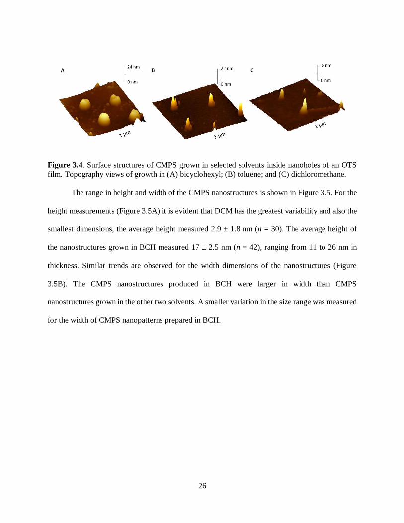
Figure 3.4. Surface structures of CMPS grown in selected solvents inside nanoholes of an OTS
film. Topography views of growth in (A) bicyclohexyl; (B) toluene; and (C) dichloromethane.
The range in height and width of the CMPS nanostructures is shown in Figure 3.5. For the
height measurements (Figure 3.5A) it is evident that DCM has the greatest variability and also the
smallest dimensions, the average height measured 2.9 ± 1.8 nm (n = 30). The average height of
the nanostructures grown in BCH measured 17 ± 2.5 nm (n = 42), ranging from 11 to 26 nm in
thickness. Similar trends are observed for the width dimensions of the nanostructures (Figure
3.5B). The CMPS nanostructures produced in BCH were larger in width than CMPS
nanostructures grown in the other two solvents. A smaller variation in the size range was measured
for the width of CMPS nanopatterns prepared in BCH.

27
Figure 3.5. Size distribution of (A) height and (B) width measurements for CMPS nanostructures
that were prepared in selected solvents.
Results of ex situ AFM experiments indicate that the binding and growth of CMPS is
highly sensitive to the nature of the solvent media. Nanostructures of CMPS exhibited more growth
in toluene and BCH than in DCM. A statistical comparison of the nanoscale dimensions of the
nanopillars of CMPS is summarized in Table 3.1, which reveals that multiple layers of molecules
were grown regardless of the solvent used to prepare samples. The nanostructures grown in BCH
showed a more uniform morphology, compared to those grown in toluene which had greater
variance in height, width and overall shape. For successful preparation of CMPS nanostructures,

28
BCH and DCM were both effective for ensuring surface growth, however DCM is not a suitable
solvent for this application.
Table 3.1. Comparison of the dimensions of CMPS nanostructures
Sample Average Height (nm) RSD % Range (nm)
bicyclohexyl 17 ± 2 15 11 - 26
toluene 24 ± 6 26 12 - 42
dichloromethane 3 ± 2 62 0.8 - 6.6
Sample Average Width (nm) RSD % Range (nm)
bicyclohexyl 220 ± 30 14 160 - 270
toluene 190 ± 40 21 110 - 280
dichloromethane 80 ± 20 25 50 – 110
3.3.3 Growth of CMPS nanostructures at selected temperatures.
Nanostructures of CMPS were grown at selected temperatures for 30 min in toluene, using
similar parameters of concentration. Samples were prepared on the same day and results were
acquired using the same AFM tip. A surface mask of silica spheres (500 nm) was used to prepare
a platform of OTS nanoholes to direct the deposition and growth of CMPS to defined sites of
Si(111). The CMPS nanostructures were characterized with high resolution AFM to directly
compare morphology differences for samples prepared at each temperature.
The CMPS nanostructures in Figure 3.6 were acquired from samples prepared at -6 ˚C, 4
˚C and 20 ˚C. The top row of images (Figures 3.6A-6C) shows representative AFM images of
CMPS nanostructures that were grown at -6 ˚C. The general morphology is similar to the previous
images in Figure 3.3D of CMPS nanostructures that were also formed in a solution of toluene. A
hexagonal arrangement of CMPS nanopatterns is viewed in Figure 6A. Adsorbates of CMPS have
deposited within the nanoholes of OTS of the surface template, with a few areas of non-specific

29
binding. The shapes and clustered morphology of the nanostructures is more clearly apparent in
the simultaneously acquired phase image (Figure 3.6B). The distance between each nanostructure
matches the diameter of the silica mesospheres that were used as a surface mask to generate the
nanopatterns. The average height measured 11 ± 5 nm (n = 45) for nanostructures that were grown
at -6 ˚C, a representative cursor profile is presented in Figure 3.6C.
Figure 3.6. Nanopillars of CMPS grown in toluene at selected temperatures. AFM results for
samples grown at -6 ˚C: (A) topography image, 1.5 x 1.5 μm2; (B) simultaneously acquired phase
image; and (C) cursor profile for the line drawn in A. Data for samples grown at 4 ˚C: ( (D)
topography image; (E) corresponding phase image and (F) cursor profile for the line in D. Results
for CMPS nanopillars grown in solution at 20 ˚C: (G) topography frame (H) phase image (I) and
cursor profile for the line in G.
Example results for CMPS nanostructures formed on a silicon substrate at 4 ˚C that were
grown for 30 min in toluene are presented in the middle row of Figure 3.6. A periodic arrangement

30
of nanostructures is revealed in the topography frame (Figure 3.6D) and corresponding phase
image (Figure 3.6E). Comparing the morphology to the samples prepared at -6 ˚C (Figures 3.6A-
6B), the morphology of the nanostructures are quite similar. There are a few nanostructures with
linear polymer branches that can be detected in the phase images. The average height of CMPS
nanostructures grown at 4 ˚C measured 16 ± 9 nm (n = 75) above the matrix film of OTS. An
example cursor height measurement for two nanostructures is shown in Figure 3.6F, revealing that
there is some variation in sizes for this sample at the nanoscale.
Images of CMPS nanostructures acquired from a sample that was immersed in a solution
of toluene at room temperature (20 ˚C) for 30 min are shown in the bottom row of Figure 3.6. The
arrangement of CMPS nanostructures is shown in the topography frame of Figure 3.6G revealing
relatively similar heights and morphology. The shapes of the clusters within the nanoholes are
visible in the corresponding phase image of Figure 3.6H. An example cursor profile (Figure 3.6I)
shows the height of two CMPS nanostructures. For samples prepared at 20 ˚C the CMPS average
size of CMPS nanostructures measured 19 ± 5 nm in height (n = 45) above the OTS matrix film.
The distribution of height measurements for CMPS nanostructures is shown in Figure 7 to
compare samples that were immersed in solutions at selected temperatures. At lower temperatures
the heights are smaller than those grown at higher temperature. The CMPS nanostructures grown
in solution at 4 ˚C resulted in structures with heights spanning from 4 nm to 43 nm, with most
nanopatterns measuring 13 nm. The range of measured dimensions is partly attributable to
variations in the sizes of the nanoholes within the OTS matrix, as well as differences in trace
amounts of water dissolved in the solvent. Two processes contribute to the size of CMPS
nanostructures, the surface self-assembly of CMPS on Si(111), as well as the subsequent growth
of multilayer structures through self-polymerization. Comparing the average values for height

31
measurements for the three chosen temperatures, distinct differences in growth were measured at
the nanoscale. We would expect that slower reaction rates at lower temperatures would produce
smaller CMPS nanostructures. Accordingly, the tallest nanostructures were observed when the
immersion temperature was increased to 20 ˚C and smaller heights were measured at colder
temperatures.
Figure 3.7. Size distribution of the height measurements for nanopillars grown at selected
temperatures.
A side-by-side comparison of representative images of CMPS nanostructures grown in
solution at selected temperatures is shown in Figure 3.8. The periodic arrangement and
reproducible shapes of the multilayered nanostructures can be distinguished from the 1 × 1 µm2
topography frames. There are four to six CMPS nanostructures within each frame with the
adsorption of CMPS mostly confined within nanoholes of the OTS matrix film.

32
Figure 3.8. Comparison of nanopillars grown at selected temperatures. Topography images of
CMPS nanostructures grown in solution at: (A) -6 ˚C; (B) 4 ˚C; and (C) 20 ˚C.
Experiments were designed to evaluate the growth and surface changes for CMPS
nanostructures at the molecular level as a function of solvent and temperature parameters. By
studying changes to isolated, well-defined nanostructures we can gain insight into the mechanisms
of surface assembly and growth. The first step of forming nanostructures is the assembly of CMPS
inside the areas of nanoholes within OTS. Exposed areas of Si(111) provide confined sites for
surface assembly to form Si-O-Si bonds to the substrate. The second step is the growth in both
vertical and lateral directions through the self-polymerization of CMPS. From previous studies it
has been proposed that multilayers form from extensive networks of Si-O bonds that result in either
a tilted or horizontal stacking of CMPS molecules through -interactions.94 Cross-linking
between molecules will produce a network to form multilayer nanostructures. The influence of
temperature for the reaction is to affect the rate of surface assembly and growth, revealing that
smaller nanostructures formed at colder temperatures due to slower assembly and growth.
3.4 Conclusions
The designed experiments were used to investigate the self-polymerization of CMPS in
solutions of selected solvents and temperatures. Particle lithography with an immersion step was
applied to generate a test platform of nanoholes surrounded by a matrix film of OTS to serve as

33
sites for the subsequent growth of CMPS nanostructures. The nanoholes within OTS provided
well-defined containers for studying the surface self-assembly and growth of CMPS. The surface
assembly of CMPS was studied ex situ with AFM for samples prepared under selected conditions
of solvent and temperature. As the solvent used for immersion of samples was changed the
resulting heights and widths of surface structures exhibited differences in dimensions, depending
on the polarity and density of the media. As the temperature was increased from – 6 oC to room
temperature the heights of nanostructures increased due to changes in the reaction rate of CMPS
binding. Nanostructures consist of multiple layers of CMPS formed by self-polymerization. By
changing the solvent in which CMPS was deposited we were able to detect morphology changes
at the molecular level for nanostructures. Changing the temperature of the immersion step was
found to influence the growth of CMPS, with colder temperatures forming smaller nanostructures.

34
CHAPTER 4. HETEROSTUCTURES OF 4-
(CHLOROMETHYL)PHENYLTRICHLOROSILANE AND 5,10,15,20-TETRA(4-
PYRIDYL)-21H,23H-PORPHINE PREPARED ON SI(111) USING PARTICLE
LITHOGRAPHY: NANOSCALE CHARACTERIZATION OF THE MAIN STEPS OF
NANOPATTERNING
4.1 Introduction
The properties of porphyrins change inherently as a result of differences in
macromolecular substituents, surface bonding mechanisms, surface orientation and coordinated
metals.102 The mechanisms by which porphyrins self-assemble on surfaces is complicated and is
an area of active investigation.103-107 The dynamics and advantages of supramolecular compounds
of porphyrins within devices and in fabricated materials are relevant for molecular studies.108-109
Properties of supramolecular films with porphyrins can be investigated with approaches such as
non-linear optics110, catalysis111 and electronic measurements.1, 112-113
Investigations of porphyrins at interfaces have focused on elucidation of magnetic,
photonic and electronic properties as well as the manner in which the molecules assemble on a
surface. The adsorption of free-base tetraphenylporphyrin on Cu(111) was studied with scanning
tunneling microscopy (STM) to evaluate the surface conformation and molecular geometry.114
Individual molecules of nonplanar freebase and copper-metallated tetraphenyl porphyrins
adsorbed on Cu(111) were investigated using frequency modulated noncontact AFM to resolve
subtle differences in structure and conformation.115 The submolecular structure of cobalt and
copper phthalocyanines on gold substrates were resolved with STM by Lu et al.116 The differences
in central metals was resolved for a mixed sample. The molecular orientation and molecular
switching properties of a triple-decker sandwich complex of phthalocyanine compounds prepared
on graphite was studied using STM by Lei et al.117
A method of photocatalytic lithography was reported for making porphyrin surface
structures that were applied for preparing protein arrays.118-119 The assembly of porphyrins at
35
interfaces has been studied using layer-by-layer assembly that incorporates organosilane or
organothiol monolayers to functionalize a surface to form multilayer films.103-104 Dip-pen
nanolithography was applied to pattern porphyrazines onto a polycrystalline gold surface to align
horizontally or vertically with a surface orientation defined by the substituents.120 The self-
assembly of manganese meso-tetra(4-pyridyl)porphyrin on Cu(111) was studied using low
temperature scanning tunneling microscopy (STM) and atomic force microscopy (AFM) to resolve
molecular structures by Chen et al.121 A functionalized phthalocyaninato-polysiloxane was studied
with STM on surfaces of highly oriented pyrolytic graphite (HOPG) by Samori et al.122
Photoelectronic devices of porphyrin polymers containing oligothienyl bridges were prepared as
microscopic junction chips and as layered diodes by Shimadzu et al.123 Multiporphyrin assemblies
have been proposed for molecular photonic devices due to the versatile physical properties.124
Particle lithography is a patterning method that uses a surface mask of colloidal spheres to
direct the deposition of molecules or other nanomaterials on surfaces. Particle lithography provides
a way to produce millions of nanostructures with reproducible shapes, sizes and arrangements with
organic thin films.97, 125 Particle lithography is also commonly referred to as nanosphere
lithography (NSL)126 and has been used to generate patterns of organic polymers, 44, 84, 95, 97, 127
nanoparticles91, 128-130 and inorganic materials.93
Experimental parameters such as the environmental conditions and solvent choice affect
the density of organosilane thin films.131-132 A model was proposed for the self-assembly of CMPS
nanostructures formed within areas of nanoholes which subsequently grew to form multiple layers
of CMPS through self-polymerization.94, 131 In a recent report, we have shown that changes in the
parameters of temperature and solvent affect the growth of CMPS nanostructures prepared within
a matrix film of organosilanes prepared with particle lithography.133
36
In this investigation, the assembly and mode of growth for attaching 5,10,15,20-tetra(4-
pyridyl)-21H,23H-porphine (H2TPyP) was studied as a model for binding porphyrins to 4-
(chloromethyl)phenyltrichlorosilane (CMPS) nanostructures within a matrix film of
octadecyltrichlorosilane (OTS). Multilayer structures of CMPS provide sites with benzyl halide
for linking porphyrins to the surface at both the top as well as at the sides of nanopatterns. Particle
lithography with successive steps of immersion reactions were used to prepare reactive surface
sites to generate multicomponent nanostructures of porphyrins and organosilanes. With ex situ
steps of particle lithography, the successive addition of molecules through chemical reactions in
solution can be evaluated by measuring changes in the heights and morphology of nanostructures.
Using high-resolution AFM, surface changes can be subsequently characterized ex situ after each
key step of the fabrication process.
4.2 Results and Discussion
An overview of the main steps for preparing nanostructures of H2TPyP within nanoholes
of OTS is presented in Figure 4.1. The growth of nanopatterns and subsequent changes in surface
morphology were characterized after each key step of sample preparation. A surface platform of
nanoholes was generated in the first step by depositing silica spheres on a silicon substrate (Figure
4.1a). The masked surface was then immersed in a solution of OTS to form a methyl-terminated
matrix film in between the silica spheres of the surface mask. The spheres were then removed with
a washing step to produce a hexagonal arrangement of nanoholes of within OTS (Figure 4.1b).
Samples with nanoholes within OTS were then placed in a solution of CMPS and either toluene
or bicyclohexyl (BCH) for a selected amount of time to generate nanodots of CMPS (Figure 4.1c).
Nanodots of CMPS formed selectively within the confined sites of nanoholes. The samples
containing the CMPS nanodots were then refluxed in a solution of H2TPyP in ethanol and

37
chloroform for 48 h to attach porphyrins (Figure 4.1d). Atomic force microscopy was used to
characterize the resulting nanostructures after each step of the fabrication procedure. The
attachment of the H2TPyP was confirmed by measuring changes in the width and height of
nanostructures.
Figure 4.1: Steps for preparing nanopatterned CMPS-porphyrin heterostructures: (a)
monodisperse silica spheres were deposited on Si(111) to form a surface mask for particle
lithography. (b) After immersion in OTS solution, the microspheres were rinsed away to reveal
nanoholes of OTS. (c) With a second immersion reaction, nanodots of CMPS were produced. (d)
Reaction with porphyrin produced taller heterostructures with spatial selectivity for the sites of
CMPS nanodots.

38
4.2.1 Surface platform of nanoholes within a thin film of OTS on Si(111)
Particle lithography with an immersion step was used to prepare nanoholes within a film
of OTS. A topographic view of the nanoholes is shown in Figure 4.2a, with the simultaneously
acquired phase image (Figure 4.2b).The ex situ images were acquired with tapping-mode AFM in
air. The topograph reveals dark nanoholes within a surrounding OTS matrix (bright areas). The
nanoholes formed a periodic arrangement throughout broad areas of microns. The distance
between each nanohole corresponds to the 500 nm diameter of the Si spheres used to form a surface
mask. The sites of nanoholes indicate the points of contact between the surface and the base of the
Si spheres. The spheres protect small local areas from assembly of OTS. There are ~40 nanoholes
in Figure 4.2a, which scales to a surface density of 108 nanoholes per cm2. Differences in tip-
sample interactions are observed between the darker exposed nanoholes of Si(111) and the
surrounding areas of the OTS matrix which are brighter, as revealed in the phase image presented
in Figure 4.2b. The surface map of phase changes indicate the changes in the viscoelastic response
that occurs between the tip and sample showing distinct differences in the interfacial chemistry of
the uncovered silicon surface within the nanoholes versus the surrounding OTS matrix.
A closer look at the hexagonal arrangement of nanoholes is presented in Figure 4.2c and
4.2d. A few bright spots on the areas of OTS reveal trace contaminants that were not rinsed from
the sample. The uniform color contrast observed in the phase image (Figure 4.2d) indicates that
the nanoholes do not contain OTS. The approximate surface coverage of the OTS film measured
97%. The average thickness of the OTS monolayer was measured to be 0.7 nm. The measurements
indicate submonolayer surface coverage relative to the ideal height (2.6 nm) of a densely packed
OTS monolayer.54, 97

39
Figure 4.2: Nanoholes within a thin film of OTS. (a) Topography frame, 3 x 3 μm2; and
simultaneously acquired (b) phase image. (c) Zoom-in topograph of nanoholes and corresponding
(d) phase image. (e) Cursor profile for the line in c.
The nanoholes within OTS that were generated with particle lithography will serve as sites
for further reactions with CMPS and H2TPyP to produce multicomponent nanostructures. Methyl-
terminated OTS was chosen to passivate the silicon surface and to serve as a resist layer to
accomplish spatial selectivity for surface reactions. The uncovered sites of Si(111) within the
nanoholes contain hydroxyl groups for binding organosilanes such as CMPS.

40
4.2.2 Preparation of CMPS nanodots
The samples with nanoholes of Si(111) within an OTS resist were immersed in a solution
of CMPS a to generate nanodots as reactive sites for further reaction. An example of the results
for preparing nanodots of CMPS is shown in Figure 4.3. Nanodots grown in a solution of CMPS
in BCH at 20 ˚C are shown in Figure 4.3a. The bright spots in Figure 4.3a are taller than the
surrounding OTS matrix. There are about 35 CMPS nanodots visible in the 3 × 3 μm2 topography
image in Figure 4.3a, which matches the surface density of OTS nanoholes. A ball-and-stick model
of a CMPS molecule indicates a length of 0.75 nm in Figure 4.3b.132 A close-up view of three
nanodots are shown in zoom-in topography and phase images in Figures 4.3c and 4.3d. The heights
and sizes of the nanodots are quite similar, without nonspecific attachment of contaminants in
surrounding areas of the OTS resist film. There is a dark outline surrounding the nanodots that is
apparent in the phase image (Figure 4.3d) which is attributable to differences in tip-surface
response at the edges of the features versus the center areas of the nanostructures. The cursor
profile in Figure 4.3e profiles the topography of two individual CMPS nanostructures that are
shown in Figure 4.3c. The heights of the CMPS nanostructures traced in Figure 4.3e closely
correspond to the average heights measured for the CMPS nanodots formed under these reaction
conditions. The height of the nanostructures measured 16 ± 3 nm (n = 35), not including the depth
of the nanoholes. The center- to-center spacing of each nanostructure measures 500 nm which
matches to the diameter of the original surface mask of Si spheres. The areas with CMPS have
self-polymerized to form multilayer nanostructures. The OTS resist confines the multilayer
polymerization of CMPS to form within the exposed nanoholes of silicon (111). The spatial
confinement promoted the vertical growth of CMPS layers, which was produced by cross-linking
to form siloxane bonds.

41
Figure 4.3: Nanodots of CMPS grown in a solution of BCH. (a) Topography image, 3 x 3 μm2;
(b) structural model of CMPS. (c) High resolution (1.5 x 1.5 μm2) topography view of CMPS
nanodots; (d) corresponding phase image. (e) Cursor profile for the line in c.
4.2.3 Spatial selectivity the for the preparation of heterostructures of CMPS and H2TPyP
Heterostructures of CMPS-porphyrin were generated by reacting nanopatterned substrates
with CMPS nanodots in a solution of H2TPyP for 48 h at 100 ˚C (Figure 4.4). Characterizations
with AFM were used to evaluate if H2TPyP bound selectively to the top of the patterns in a vertical
growth process, or if the structures also became taller due to horizontal growth through binding at
the sides of the nanodots. The surface placement of 45 CMPS-porphyrin nanostructures are shown

42
within the 4 × 4 μm2 area of the topography image of Figure 4.4a. The hexagonal arrangement of
nanopatterns is maintained with center-to-center spacing between nanostructures measuring 500
nm, as revealed in the close-up topography and phase views (Figure 4.4b and 4.4c). There is little
nonspecific binding on the OTS matrix areas between the nanostructures, as shown in the phase
map of Figure 4.4c. An example cursor profile that was traced across two heterostructures indicates
the heights of the heterostructures range from 30 to 40 nm (Figure 4.4d). The average height of
the CMPS-porphyrin heterostructures measured 24 ± 6 nm (n = 35), this is an increase of ~8 nm
from the size of the CMPS nanodots.
The nanostructures of CMPS also showed growth in lateral dimensions after the addition
of the porphyrin. A comparison of the nanostructure surface coverage was conducted to evaluate
lateral growth of the nanostructures before and after porphyrin addition. The percentage surface
coverage of the nanostructures was measured from multiple sites on each of the surfaces (before
and after porphyrin addition). The average surface coverage of the CMPS nanostructures was 2.3%
of the surface. After porphyrin addition, the surface coverage increased to 4.6%. The difference in
surface coverage was determined to be statistically significant at a 98% confidence level. The
change in surface coverage is evidence of growth in the lateral dimensions of the CMPS-porphyrin
nanostructures and confirms that porphyrin has attached to the CMPS nanodots.

43
Figure 4.4: Heterostructures comprised of CMPS and porphyrin. (a) Topography image (4 x 4
μm2) of porphyrin nanostructures grown on CMPS nanodots. (b) Zoom-in topography view of
porphyrin heterostructures; (c) simultaneously acquired phase image; (d) cursor profile for the line
in b.
4.2.4 Proposed model for constructing heterostructures of CMPS and H2TPyP
The reaction for producing CMPS nanodots is driven by hydrolysis and condensation
reactions that promote the vertical growth of the CMPS nanodots through crosslinking siloxane
bonds.133 We did not observe evidence of branching or growth in lateral dimensions for CMPS
nanodots, the growth was directed in the vertical direction to create taller nanostructures.

44
However, the nanodot structures became taller and wider after reaction with H2TPyP. A possible
model of how growth of H2TPyP occurs in both vertical and horizontal directions is presented in
Figure 4.5. Nitrogen containing pyridal groups that are substituents of the porphyrin act as an
electrophile in the nucleophilic replacement of the benzyl halide that is exposed at the outer regions
of the CMPS nanostructure. Previous studies without nanopatterning steps investigated the
application of CMPS as a coupling layer for the addition of H2TPyP to produce a porphyrin thin
film 103-104. Multilayer films are stabilized by siloxane bonds that form the backbone of the CMPS
linker, as well as by weaker pi-pi interactions between the benzene rings of CMPS and the
porphyrin macrocycles.
Figure 4.5: Model for the self-assembly of CMPS-porphyrin heterostructures within an OTS
matrix layer.
4.3 Conclusion
Particle lithography was applied to generate nanopatterns to determine the surface
placement of porphyrin-CMPS heterostructures. Nanoholes were used to spatially direct the
fabrication of complex nanostructures on Si(111) using multiple steps of immersion reactions
45
combined with particle lithography. Periodic arrangements of heterostructures of CMPS-H2TPyP
heterostructures were generated through a multistep layer-by-layer assembly process. A film of
methyl-terminated OTS provided an effective resist for preventing nonspecific adsorption or
reactions on areas between nanopatterns during successive chemical steps. Nanodots of CMPS
were used as a linker for binding porphyrins to the surface. The changes in surface morphology
were examined after each step using ex situ AFM studies. A model was proposed for attachment
of H2TPyP to CMPS nanodots with growth observed in both the vertical and lateral directions.
Particle lithography provides a practical tool for evaluating surface growth and changes for
multistep chemical reactions.
4.4 Experimental Section
4.4.1 Materials and reagents
The porphyrin selected, 5,10,15,20-Tetra(4-pyridyl)-21H,23H-porphine (H2TPyP) (97%)
was obtained from Sigma Aldrich (St. Louis, MO). Anhydrous ethanol (200 proof) was purchased
from Pharmco-Aaper (Shelbyville, KY). Cloroform, (HPLC grade) was obtained from Avantor
Performance Materials (Center Valley, PA). Octadecyltrichlorosilane (97%) and (p-
chloromethyl)phenyltrichlorosilane (95%) were purchased from Gelest (Morrisville, PA).
4.4.2 Preparation of OTS nanoholes within an OTS matrix film
Particle lithography was used to prepare nanoholes within a thin film of OTS on Si(111).
Silicon wafers (Ted Pella Inc. Redding, California) were rinsed with water and cleaned in piranha
solution (3:1 sulfuric acid to hydrogen peroxide) for 1.5 h to remove surface contaminants.
Caution: this solution is highly corrosive and should be handled carefully. The substrates were
then rinsed with ultrapure water and dried under nitrogen. After drying, 10 μL of monodisperse
silica microspheres in water was deposited on the clean silicon substrates and dried in air to

46
produce a surface film of Si spheres. The substrate and dried microspheres were placed in an oven
at 150 ˚C for 20 h. The annealing heating step is used to temporarily solder the silica microspheres
to the silicon surface so they were not displaced in solution. The substrates containing the silica
microspheres masks were then removed from the oven and placed in a 0.1% (v/v) solution of OTS
in toluene for 5 h. The samples were then rinsed with ethanol and water with successive sonication
in ethanol, ultrapure water, and chloroform. The rinsing and sonication step was used to fully
remove the spheres from the surface. The samples were then dried under argon and characterized
with AFM.
4.4.3 Fabrication of CMPS nanostructures.
The samples with nanoholes within OTS were immersed in a 0.6% solution of CMPS in
either anhydrous toluene or bicyclohexane (Sigma Aldrich, St. Louis, MO) for 30 min. After the
immersion step, samples were rinsed and sonicated in ethanol and chloroform. The samples were
then dried under nitrogen and subsequently characterized with AFM.
4.4.4 Preparation of heterostructures of CMPS and porphyrins
The samples with CMPS nanodots within an OTS matrix were immersed in a solution of
H2TPyP in ethanol (1.8 mM) and chloroform (ratio of 1:9 respectively) and refluxed at 90˚C for
48 h. The samples were removed and rinsed with ethanol, then sonicated in chloroform and ethanol
for 5 min. The sonication step was repeated 4 times and then the samples were dried under
nitrogen.
4.4.5 Atomic force microscopy
Samples were characterized using a Model 5500 atomic force microscope (Keysight
Technologies, Santa Rosa, CA). Images of sample were acquired using tapping-mode in ambient
air. Silicon nitride tips that have force constants ranging from 10 to 30 N/m, and resonance

47
frequencies ranging from 265 to 280 kHz ((Nanosensors, Neuchatel, Switzerland) were used for
AFM studies. Digital images were processed using the open source software Gwyddion, which is
supported by the Czech Metrology Institute.134
Acknowledgments
The authors gratefully acknowledge financial support from the Louisiana Board of Regents
Support Fund Traditional Enhancement Program (LEQSF(2014-16)-ENH-TR-03).

48
CHAPTER 5. INVESTIGATION OF THE SELF-ASSEMBLY OF PORPHYRIN
NANOSTRUCTURES AND THIN FILMS USING PARTICLE LITHOGRAPHY
STUDIED WITH ATOMIC FORCE MICROSCOPY
5.1 Introduction
The synthesis of new tetrapyrroles and efficient routes to fabricate novel nanostructures is
a field of inexhaustible interest. Investigations of porphyrin and phthalocyanine self-assembly
serve to advance their molecular electronic functions as materials within an array of devices
including, organic photovoltaic devices, organic light emitting diodes, wires, capacitors,
phototherapeutics, and many more organic based technologies.105, 135-141 As these technologies
progress, the current paradigm persists in the miniaturization of their electronic components to
maximize device capabilities and to utilize every nanometer available to boost device performance.
This persistence creates a demand for new, novel porphyrin and other related macrocycles that can
self-assemble to form larger, more complex multi-component systems on a surface.
Understanding, on a molecular level, how these engineered porphyrin bind to and grow from
surfaces is paramount in truly understanding their potential moving forward.
Many synthetic strategies can be applied to engineer molecules and nanostructures, where
both the substituents and central coordination sites can be utilized to tune molecular characteristics
and generate supramolecular systems that can self-assemble into solid state materials.142-143 The
mechanism by which these supramolecular systems self-organize on a surface is still actively
investigated and not always understood. There are complexities that arise from the interactions
between the supporting substrate and the supramolecular porphyrin materials that can result in
unique and novel functions. Through recent advances, nanostructures of porphyrin and
phthalocyanine derivatives have been successfully generated through synthetic routes and grown
from surfaces via a silane coupling reaction on surfaces of silicon, glass, and ITO.1, 144-145 The
fabrication of these porphyrin and phthalocyanine nanostructures was accomplished via the

49
utilization of a silane coupling reaction. This silane coupling reaction has been previously used for
the fabrication of nano and micro scale materials as well as for the functionalization of silicon
based and electrode surfaces.138, 146-148 There have also been many studies in which porphyrin, and
silicon porphyrin nanostructures were probed to characterize their morphologically dependent
electronic characteristics, both in solution and in schemes where the nanostructure were grown
from surfaces.1, 104, 112-113, 144
Many studies are limited by difficulties that arise during the characterization of
supramolecular structures at the nanoscale. Supramolecular porphyrin assemblies, such as
nanorods, nanowires and nanodots, cannot be deposited or grown from a surface because they are
not able to chemisorb or covalently bind to the surface. These limitations results in an inability to
selectively pattern tetrapyrrole supramolecular structures. Due to the structural nature of
tetrapyrrole molecules, their supramolecular organization is affected and driven by several
different forces including metal-ligand bonds, non-covalent ionic bonds, hydrogen bonding, -
interactions and other intermolecular forces including van der Waals forces.142, 149-150 Ultimately
this leads to a tendency for porphyrins to self-aggregate and form stacked or layered arrangements
on a surface. Previous studies have demonstrated the utility of self-assembling organosilane thin
films to fabricate and covalently bind porphyrin to surfaces of silicon and glass.103-104 This strategy
has been advanced upon in more recent studies where practical approaches were employed to
incorporate particle lithography to fabricate nanoscale organosilane and thiol platforms that can
be applied to spatially confine and study self-assembly at selective sites.44, 97, 113, 137, 151 By
combining methods of particle lithography and a silane coupling reaction, porphyrins and
phthalocyanine nanostructures can be engineered with nanoscale selectivity and high through-put
capability.44, 126-129, 152
50
5.2 Materials And Methods
5.2.1 Atomic Force Microscopy.
All samples were analyzed using a Model 5500 atomic force microscope (Keysight
Technologies, Santa Rosa, Ca). All images were acquired using either tapping mode or contact
mode AFM. Non-conductive silicon nitride tips were used to acquire all images and tapping mode
images were acquired with tip that had a spring constant ranging between 10 and 130 N/m and an
average resonance frequencies ranging from 272 to 464 kHz (Nanosensors, Neuchatel,
Switzerland). All images shown were processed using Gwyddion open source software, which is
supported by the Czech Metrology Institute.134
5.2.2 Preparation of Silane Porphyrin Thin Film.
Immersion deposition was used to generate a thin film of silicon OEtP (TCI Chemc on
surfaces of Si(111). Pre-cut polished silicon wafers (Virginia Semiconductor, Frederickburg, VA)
were rinsed with ultrapure water and then immersed in a piranha solution for 1.5 h to remove
surface contamination and increase the number of hydroxyl groups on the surface. Caution:
piranha solution (a mixture of hydrogen peroxide and sulfuric acid with a (v/v) ratio of 1:3) is
highly corrosive and should be handled with great care. After the 1.5 h immersion in piranha, the
substrates are removed and rinsed again with ultrapure water. The silicon coordinated porphyrin
thin films were formed by adding silicon tetrachloride (purchased from TCI) to a 0.5 mM solution
of 2,3,7,8,12,13,17,18-octaethylporphyrin (purchased from TCI) in chloroform. The cleaned
silicon substrates were added to the OEtP solution to react for 5 h. The substrates were then
removed, rinsed with ethanol and ultrapure water and then sonicated in chloroform. The samples
were then dried under nitrogen and characterized with AFM.
5.2.3 Preparation of Silane Porphyrin Nanopatterns.

51
Precut polished silicon wafers were subjected to the same cleaning procedure noted before.
A microsphere solution was prepared by first washing with centrifugation to remove contaminants.
After centrifugation the microsphere pellet was separated by decanting the water supernatant and
replaced with new ultrapure water. The microspheres were suspended again within solution via
vortex mixing. This process was repeated several times before a 10 μL aliquot was deposited onto
the surface and dried in air. Once dry, the substrates were placed into an oven at 150 ˚C for a
controlled period time. The substrates were then either placed in air before being moved to the
reaction vessel or immediately moved to the reaction vessel and placed into a 0.5 mM solution of
OEtP in chloroform with a molar excess of silicon tetrachloride. The substrates were immersed for
5 h and then removed and cleaned by rinsing in ethanol and then water before sonication in
chloroform. The samples were dried under nitrogen and then characterized using AFM.
The same procedure was used to prepare nanoholes within a thin film of OTS that could
be used to selectively nanopattern pillars of silicon OEtP. The silicon substrates were cleaned and
the microspheres were prepared and deposited in the same fashion noted before. After the
substrates (with microspheres deposited on surface) were removed from the oven, they were
immersed in a 0.1 % solution of OTS and allowed to react for 5 h. The sample was then removed
and rinsed with ethanol and ultrapure water before being sonicated in ethanol and water separately.
After the presence of nanoholes was confirmed the samples were immersed in a solution 0.5 mM
solution of OEtP in chloroform with a molar excess of silicon tetrachloride to react for 5 h. After
the immersion was complete, the samples were removed and rinsed in ethanol and water followed
by sonication in chloroform before being characterized via AFM.

52
5.3 Results and Discussion
Figure 5.1. Procedure for generating nanoholes within a thin film OEtP. (A) Silica microspheres
are deposited on cleaned substrate of Si(111). (B) The silicon substrate with the microsphere
mask was immersed in a single pot solution of OEtP, silicon tetrachloride and chloroform. (C)
the sample containing the nanoholes of Si(111) within a film of OEtP was rinsed and
characterized with AFM.
5.3.1 Steps for Preparing Porphyrin Nanostructures and Thin Films.
The step by step process for fabricating porphyrin nanostructures on Si(111) is detailed in
Figure 5.1. A solution of monodisperse silica microspheres was rinsed and then deposited onto a
piranha cleaned substrate and dried in air. Through natural capillary forces the silica microspheres
form close-packed layers on the atomically flat silicon surface (Figure 5.1A). This layered silica
microsphere assembly served as a surface mask for the generation of a functionalized porphyrin
surface. The areas directly contacted by the microspheres are masked from reaction with silane
functionalized porphyrin macrocycle. After the substrate and microsphere solution are dried in air
they are then placed in an oven to anneal the silica beads to the surface to prevent them from being
washed away or lifted from the surface during the immersion deposition step of the process. Trace
amounts of water are necessary to initiate the hydrolysis and condensation reactions that drive and
control the assembly of silane films and structures.44, 151 By controlling the amount of available
water on the surface, one can select the resulting nanostructure produced during the immersion

53
deposition process. After the silica microsphere soldering step the masked substrate is placed into
the 0.5 mM OEtP solution in chloroform. To this solution a molar excess of silicon tetrachloride
is added to initiate the porphyrin-silane coupling reaction (Figure 5.1B).1 In Figure 5.1C
nanopores of unreacted Si(111) are furnished within a thin film of OEtP. The depth of this film
can be controlled temporally with thicker films formed over longer immersion periods.1
Figure 5.2. Procedure for preparing OEtP nanopillars within a resist of OTS. (A) Nanopores of
Si(111) within OTS are prepared using techniques of immersion particle lithography. (B)
Substrates containing nanoholes are then immersed in OEtP single pot reaction solution to react
for several hours. (C) The substrates are removed and characterized with AFM to reveal
nanopillars of OEtP.
The fabrication of OEtP nanopillars within a resistive octadecyltrichlorosilane (OTS) film
was accomplished via the combination of particle lithography and successive immersion
deposition steps. The schematic in Figure 5.2 contains the steps for selectively depositing OEtP
54
nanopillars into nanoholes within a thin film of OTS. The nanoholes of Si(111) within the thin
film of OTS serve to direct and confine the self-assembly and subsequent vertical layer by layer
assembly of OEtP. Nanoholes of Si(111) provide for new ways to study porphyrin self-assembly
by confining the porphyrin’s initial surface assembly mechanism to small attoliter size reaction
vessels (nanoholes). The number of nanopillars that can be generated on a given surface is
controlled directly by the diameter of the microspheres chosen to mask the surface, with more
structures being generated when smaller diameter microspheres are used in the lithography step.97,
151 The schematic in Figure 5.2A shows a surface where particle lithography was used to generate
nanoholes within a thin film of OTS. Once prepared, these discrete areas are still available to
undergo surface attachment, whereas the surrounding matrix has now been passivated and is no
longer capable of reacting with the porphyrin complex. By confining the growth of OEtP, greater
insight can be gained into the mechanism by which it assembles on the surface and forms
multilayer nanostructures. The next step (Figure 5.2B) involves a single pot reaction vessel where
the substrate with nanoholes is placed into the porphyrin solution and silicon tetrachloride is added
to initiate the porphyrin-silane coupling reaction and further surface assembly. After the substrate
has been immersed in the porphyrin solution, it is removed and cleaned with chloroform and water
before the nanopillars are characterized via AFM (Figure 5.3C).
The nanopillars assemble at the site that were previously nanoholes. Trace amounts of
water still reside in the discrete areas if hydrophilic nanoholes that were created in the previous
steps. This trace amount of water initiates a series of hydrolysis and condensation reactions that
drive the surface attachment of OEtP nanopillars as well as the layer by layer assembly. The longer
the substrate is left in the porphyrin solution the taller the nanopillars grow.1

55
Figure 5.3. Growth of OEtP thin film with the addition of silicon tetrachloride. (A) Topography
image of silicon surface after immersion in a solution of OEtP without silicon tetrachloride. (B)
the corresponding phase image to (A). (C) Topography and simultaneously acquired (D) phase
image of OEtP film deposited through immersion in a solution of OEtP with silicon
tetrachloride.
5.3.2 Analysis of Porphyrin Thin-film Growth.
The surface assembly of OEtP is dependent entirely upon the reaction with silicon
tetrachloride. Only through the coordination of silicon is the porphyrin able to partake in the
hydrolysis and condensation reactions that enable it to self-assemble and grow from a surface
functionalized with hydroxyl groups. This point is examined in Figure 5.3. The top row of Figure
5.3 contains images of a silicon substrate that has been immersed in an OEtP solution for 5 h
without the addition of SiCl4. The topography in Figure 5.3A reveals an atomically flat silicon

56
surface with an RMS roughness of 122 pm. The corresponding phase image (Figure 5.3B) shows
the presence of very few impurities across the 6 × 6 μm2 surface. In the bottom row, topography
(Figure 5.3C) and friction (Figure 5.3D) images reveal evidence of a porphyrin thin film grown
from the bare silicon substrate. The Rrms roughness of this substrate measured 3.8 nm, a substantial
increase from the previously viewed surface of bare silicon. The topography image (Figure 5.3C)
reveals a relative uniform growth of the porphyrin film, which is thermodynamically controlled by
the rates of the hydrolysis and condensation reactions that help it form. The film itself is made up
of what appear to be smaller well defined pillars of OEtP. In the friction image (Figure 5.3D) there
are clearly defined realms that reveal through to the silicon surface. These areas appear darker in
the friction image because the tip experiences a relative change in friction between the OEtP thin-
film and the bare surface of Si(111).
Figure 5.4. Absorbance spectra of OEtP solution before (red) addition of silicon tetrachloride
and after (purple) silicon tetrachloride was added.

57
The different surfaces shown in the top and bottom row of Figure 5.3 help to elucidate the
significance of SiCl4 in the self-assembly of OEtP on Si(111). In Figure 5.4 two absorbance spectra
are shown. Both are of a 0.5 mM solution of OEtP. The red line is the absorbance spectra of OEtP
in solution with no SiCl4 added. This spectra matches the anticipated and previously observed
spectra of OEtP. A shift occurs with the addition SiCl4 and can be observed in the purple line of
Figure 5.4. The notable red shift is accompanied by a rapid color change in the porphyrin solution.
This shift is also accompanied by the loss of a Q-band peak that originally occurred at 620 nm.
This shift is indicative of an increase in electronic communication between the porphyrin rods in
solution. We hypothesize that this increase in electronic communication is the consequence of
porphyrin rod formation that results from the silicon coordination by the porphyrin. This
coordination would enable subsequent assembly and attachment of individual porphyrin
macrocycle via the establishment of an interlinking siloxane backbone1, 144-145
5.3.3 Characterization of Porphyrin-silane Nanostructures.
The microsphere masks that are deposited on the silicon substrate effectively serve to block
the porphyrin-silane molecules from adsorbing at the microsphere’s direct points of contact and
instead drive the molecules to assemble at the interstitial sites. At these interstitial sites there is
also a layer of water that develops on the surface; and this trace amount of water initiates the
molecules self-assembly. This thin film of water can be controlled to selectively generate specific
types of nanostructures. The amount of water present on the surface can controlled by altering the
drying conditions before the immersion deposition step.44, 151, 153 The microspheres that are
deposited on the surface help to spatially direct and control the trace amounts of water on the

58
surface as well. Through the combination of control over these variables, nanostructures of
selectable morphology can be fabricated with high throughput.
Figure 5.5. Nanoholes of Si(111) within a film of OEtP prepared using particle lithography. (A)
Topography view of OEtP nanoholes and (B) phase image of the same area, 3 × 3 μm2. Cursor
profile of the line traced in the former topography view.
Figure 5.5 contains images of nanoholes of OEtP on Si(111). These nanoholes were
generated by depositing a solution of 500 nm silica microspheres on a cleaned surface of Si(111)
and then dried in air for several hours. The substrate was briefly placed in an oven to anneal the
silica microspheres to the surface and then left out in ambient conditions for several hours. The
substrate with the microspheres was then added to a solution of OEtP and SiCl4. It was left to react
at room temperature in a closed vial for 5 h. The modified substrate was removed, rinsed with
ethanol and chloroform, followed by sonication in chloroform. The samples were then

59
characterized via tapping-mode AFM. The trace amount of water on the surface was distributed
homogenously, resulting in the formation of nanopores of OEtP-silane, as seen in the topography
image (Figure 5.5A). The corresponding phase image (Figure 5.5B) was acquired simultaneously
and further reveals the nanopores of exposed Si(111) which appear darker relative to the
surrounding OEtP-silane nanopillar film. In Figure 5.5C a cursor profiles traces the line mapped
across two nanoholes in the topography image. The average depth of the nanoholes was measured
to be ~ 7 nm (n = 61) The cursor profile help to show the roughness of the OEtP Film that formed
in the interstitial sites between the nanoholes. The Rrms of these interstitial areas was measures to
be 1.8 nm. The surface coverage of the thin OEtP-silane film was measured to be 95.6 %.

60
Figure 5.6. Fabrication of OEtP nanorings on Si(111). (A) Topography view of nanorings, 3 × 3
μm2, and simultaneously acquired (B) phase image. Zoom-in view (600 × 600 nm2) of a single
OEtP nanoring and simultaneously acquired (D) phase image. (E) Cursor profile of the line
traced in the (C) zoom-in topography image.

61
Alternatively, nanorings of OEtP-silane can be generated by first adding the substrate, with
deposited microspheres, to an oven at 150 ˚C for roughly 20 h. This longer annealing time served
to drive off enough of the nanoscopic amounts of water, to leave the trace amount of water left on
the surface to assemble at the very base of the microspheres. This drying condition allows for the
surface water to be spatially controlled when combined with particle lithography. In Figure 5.6A,
there is a 3 × 3 μm2 topography image of nanorings that were fabricated under these conditions.
There are ~ 30 nanorings within this area, which corresponds to ~ 108 nanostructures within a 1 ×
1 cm2 area. The number of nanostructures per given cm2 can be increased by decreasing the
diameter of the microspheres used to mask the surface. The phase image in Figure 5.6B
corroborates the significance of the water to initiate the absorbance of the OEtP-silane on Si(111).
There is very little evidence of non-specific or interstitial OEtP-silane growth, it has been confined
to the specific areas on the surface where water residues were. A zoom-in topography view (Figure
5.6C) shows a single nanoring that is made up of many smaller nanostructures. The corresponding
phase image (Figure 5.6D) reveals further morphological details regarding the viscoelastic nature
of the porphyrin nanorings versus the inner and outer areas of bare silicon surface. It appears that
many of the small nanostructures grew vertically from the surface, and are limited to these few
areas directly around the base of where the microsphere previously sat. The cursor profile of the
single ring (Figure 5.6E) reveals several layers of varying thickness within one nanoring structure.
The average height of the nanorings was measured to be 3.5 nm (n = 27).

62
Figure 5.7. Nanopatterns of OEtP self-assembled nanopillars within thin film of OTS. (A)
Topography view of OEtP nanopillars, 3 × 3 μm2, and corresponding (B) phase image of the
same area. (C) 3-D view of OEtP nanopillars of the same area.
In Figure 5.7 nanopillars of OEtP were generated from nanopores within an OTS matrix.
The previous nanostructures were grown through particle lithography and the manipulation of
nanoscopic volumes of water on the surface. However, in this final segment, attoliter volume
nanoholes were used as reaction containers to study the self-assembly to OEtP nanostructures at
the molecular level. First nanoholes within OTS were generated using particle lithography. The
substrates were then reacted in a vessel contain OEtP in solution with SiCl4, followed by the same
rinsing and sonication steps as all other OEtP samples. The resulting nanopillars assembled and
grew from the nanoholes vertically with the individual porphyrins stacking face to face. The

63
resulting nanopillars are stabilized via a siloxane bond that runs through the center of the each
porphyrin, Si-O-Si, and also by intermolecular -interactions. The topography image in Figure
5.7A, a 3 × 3 μm2 area contains about 30 nanopillars, roughly matching the number of
nanostructures observed in the previously shown images. These nanopillars are patterned
hexagonally with a structure to structure distance that matches the diameter of the microspheres
used to form the mask. The matching phase image in Figure 5.7B reveals structures that are
morphologically different than the previous nanostructures of OEtP-silane. These pillars possess
some evidence of fractured growth and multiple domains within a single nanopillar, however,
many appear to be much more homogenous. The 3-D view in Figure 5.7C provides insight into
the very comparable heights of the nanostructures that were grown over a 5 h period. There is also
very little evidence of non-specific growth across the OTS matrix. This signifies that the OEtP-
silane molecules have a very high specificity for the nanoholes and equally towards the available
Si-OH bonds that terminate the head group of each pillar during the layer by layer growth
mechanism.

64
Figure 5.8. Histogram of OEtP nanopillar heights.
Figure 5.8 contains a histogram of the nanopillar heights. The average height of the
nanopillars was measured to be 29 ± 4.6 nm. The heights from the histogram in Figure 5.8 match
these averages and reveal a small relative range of heights that most of the nanopillars grew to.
The heights ranged from 24-47 nm, revealing that the majority of nanopillars experienced very
similar growth rates, with few experiencing abnormally fast growth. Previous studies have shown
that the heights can be selectively tuned by controlling the substrate immersion time.1 The role and
nature of organosilane chemistry results in the production of highly controlled and densely
patterned OEtP-silane nanopillars.
5.4 Conclusions
Using a silane coupling reaction combined with particle lithography, silicon-OEtP
nanostructures and thin films were patterned with spatial selectivity and nanoscale control. OEtP-
silane nanostructures of nanopores, nanorings, and nanopillars were fabricated on surfaces of

65
Si(111) by selectively adjusting the drying conditions to control the residual water on the silicon
surface. Each nanostructure formation consisted of multiple layers of porphyrin that assembled
from the surface through a siloxane backbone that resulted in a co-facial stacking of the
macrocycle. This data provides new direction for the spatial patterning of silicon porphyrin
complexes that cans furnish surfaces with new intriguing nanoscale function.

66
CHAPTER 6. IMAGING AND PROCESSING ARTIFACTS COMMONLY
ENCOUNTERED IN ATOMIC FORCE MICROSCOPY SURFACE
CHARACTERIZATION
6.1 Introduction
Atomic force microscopy was first developed in 1986 by Binnig, Quate and Gerber.2 The
data that is acquired with AFM is generated through physical interactions between the tip and the
sample surface.154-157 The interactions between the tip and the sample inherently affects the
measurements acquired and these measurements will have observable unnatural and unexpected
features as a result. The source of the majority of these artifacts can be grouped in to four main
categories in AFM: the cantilever tip, the scanner, image processing, and
environmental/vibrations.3 These artifacts can vary in complexity in with some being more
difficult to anticipate, identify and correct for than others. Identification of artifacts is imperative
when imaging and subsequently addressing the data that is obtained from this characterization
technique.
Since the invention of AFM, studies have been conducted to investigate the sources and
nature of artifacts that arise from surface imaging and post-acquisition processing of scanning
probe data.3, 158 The sources of artifacts are in part associated with the physical setup of an
atomic force microscope, as well as the software used to interpret and transduce this data into an
image. Figure 6.1 is a schematic representation of a common scan-by-tip instrument setup. In the
schematic there is a piezo tube scanner that contains the X, Y, and Z piezo-ceramic materials that
are responsible for positioning the tip on the surface with nanometer scale control. At the end of
the reflective cantilever there is a micro-fabricated tip whose dimensions are known within a
given range. This tip is brought into contact with the surface and a laser is reflected off the back
of the cantilever onto a reflective photodiode to a specific point that is determined by the user as

67
the driving signal set point in contact mode AFM. In tapping mode AFM the driving signal set
point is based upon an oscillation amplitude that is set by the user and is near the tip-piezo
resonance peak. This driving signal will be constantly compared to the measured signal that will
change as the tip is scanned across the surface in a raster fashion. The data obtained is gathered
based upon the difference in the measured signal versus the driving signal, commonly referred to
as the error signal. The feedback loop manages how fast the piezo-ceramic material in the
scanner will react and change to restore the measured signal back to the driving signal. All of
these different components have associated artifacts that can be observed while imaging.
Understanding how AFM works and the function of each component is paramount in the effort
to better identify and correct and the artifacts that can arise.
Figure 6.1. Schematic of scan-by-tip atomic force microscopy
6.1.1 NANOSTRUCTURES GENERATED USING PARTICLE LITHOGRAPHY
Many of the figures and images shown here are of nanostructures that were generated
using particle lithography techniques. Particle lithography has been previously used to pattern

68
arrays of (SAMs), proteins, polymers, and nanoparticles on a variety of surfaces that include,
gold, mica, quartz, silicon, and indium tin oxide (ITO).84-92 This high- throughput lithography
technique can be coupled with varying organosilane deposition protocols to generate tunable
nano-scale architectures.97
Figure 6.2. Procedure for generating nanostructures and nano-platforms via particle lithography.
Top row utilizes particle lithography and immersion deposition to generate pattered nanopores of
confined surfaces for reaction. The bottom row shows particle lithography combined with vapor
deposition techniques to generate nano-ring structures of the chosen SAM.
Two common deposition techniques that incorporate particle lithography are shown in
Figure 6.2. These approaches each involve particle lithography however, by changing the
specific organosilane or organothiol deposition technique, different nanostructure patterns can be
generated. Vapor deposition can be used to generate nanorings and immersion deposition can be
used to generate nanopores.97 The density of these patterns can be tuned by choosing
microspheres of larger or smaller diameters. In each of these patterns discrete areas of the
original surface are masked by the mesosphere and are still available for further surface

69
modification after the initial passivation step. Many of the architectures generated in this paper
are generated via this bottom up strategy where nanoparticles, organosilanes, and porphyrins
were bound to these specific confined reaction areas.
6.2 Probe Artifacts
The nature of the tip and the physical basis of scanning probe microscopy inherently affects
the measurements and images that are acquired. The majority of scanning probe artifacts fall into
the category of probe artifacts because of the probes nature in this measurement system. As the
tip is scanned across the surface, information regarding the surface and tip is being simultaneously
recorded. The tips geometrical shape will always affect the facets and features of the surface it is
measuring.159 The sharper the tip, relevant to the features of the surface, the more accurate the
images of the surface features will be. The geometries of the surface features affect the quality of
the image based upon how they compare to the geometries of the tip.159 Surface features with
higher aspect ratios or smaller facets require measurement by tips with equally greater aspect ratios
in order to successfully trace the truest geometries of that feature. These are general rules that must
be accounted for when choosing the correct probe to characterize a given surface.
To help mitigate the effects of the of poor tip-sample interactions, due diligence is
necessary when determining which probes are best suited for particular surfaces. Several factors
affect the tip’s ability to accurately track the sample surface. The tips sharpness is one of the most
important and obvious, but other factors include, tip-sample adhesion force, probe force
magnitude, sample elastic properties, surface properties and sample environment i.e. thermal
noise.160-163 By better understanding the nature of tip-sample interactions and general properties
of a tip, a higher quality image with more accurate surface mappings can be obtained. In the
following paragraphs specific examples of common tip artifacts will be depicted with details

70
concerning the nature of the artifact as well as the most effective process for correction. The
artifacts shown below are on surfaces comprised of nanostructures that were generated with and
within organosilane self-assembled monolayers (SAMs).
6.2.1 Tip Convolution
Tip convolution or “dilation” occurs most often when the probe being used to characterize
a surface is too large and or blunted to accurately map the true dimensions of the surface features
being imaged. This often results in surface features that appear to be too large (objects protruding
from the surface) or too small (nanoholes). When imaging features with particularly small
dimensions such as nanoparticles, the resulting image will inherently suffer some width
broadening. The height of the surface features can be measured to accurately assess the true size
of such samples on a surface. These artifacts are always present in to some degree and the extent
of this convolution typically worsens with time as the tip is used and its sharpness is dulled. Tip
convolution can be easily recognized on surfaces where specific features don’t match their
anticipated size (i.e. particles appear too large or holes appear smaller).
Figure 6.3 contains topography and phase images of spherical nanoparticles where the top
row of images are characterized with a tip that is blunted. The features of the nanoparticles are
dulled and the widths broadened as a result of using a tip with blunted dimensions that were too
large relative to the size of the nanoparticles being characterized. The schematic in the top row of
Figure 6.3 visually depicts this aspect ratio mismatch that leads to the tip-sample convolution. As
the tip is scanned across the surface, the edge or side of the tip comes into contact with the
nanoparticle on the surface altering the forces experienced between the tip and sample that initiate
the feedback mechanism to adjust the position of the tip relative to the surface.
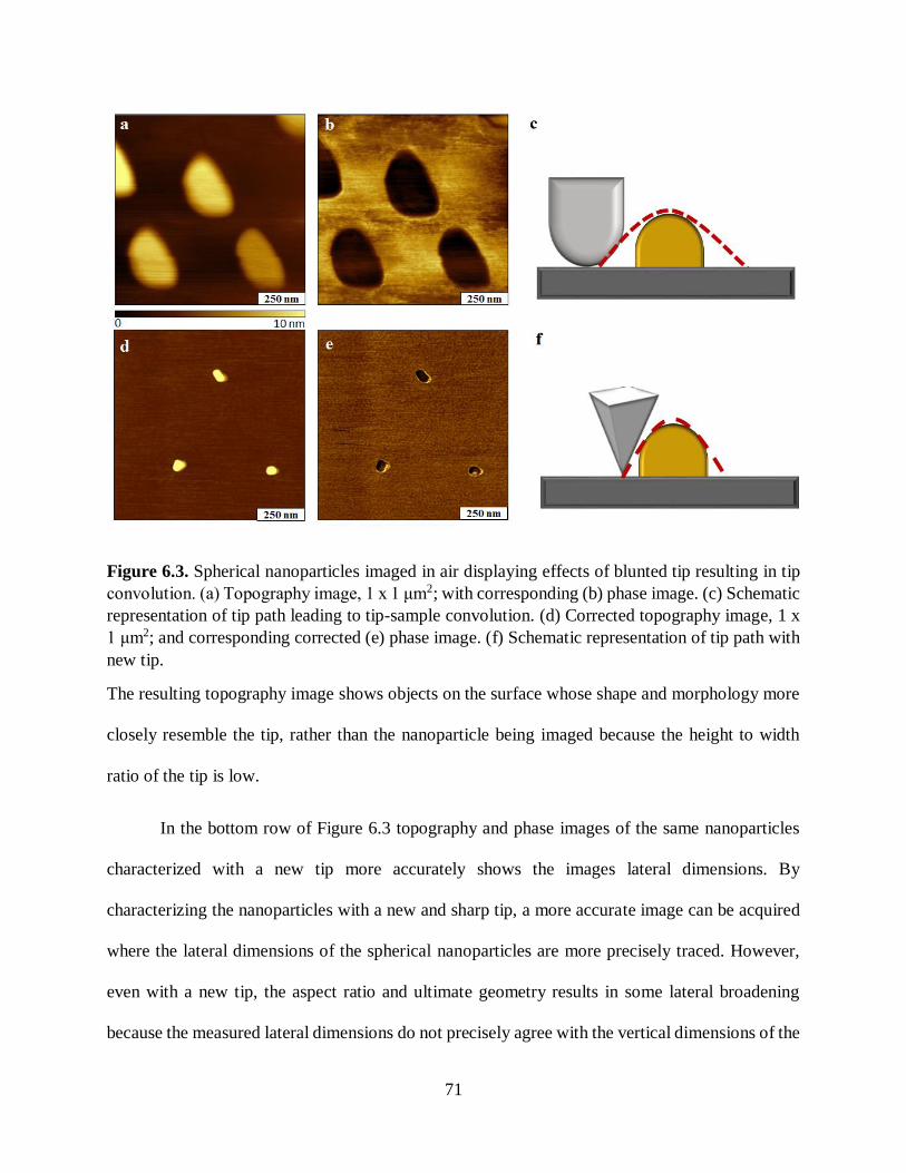
71
Figure 6.3. Spherical nanoparticles imaged in air displaying effects of blunted tip resulting in tip
convolution. (a) Topography image, 1 x 1 μm2; with corresponding (b) phase image. (c) Schematic
representation of tip path leading to tip-sample convolution. (d) Corrected topography image, 1 x
1 μm2; and corresponding corrected (e) phase image. (f) Schematic representation of tip path with
new tip.
The resulting topography image shows objects on the surface whose shape and morphology more
closely resemble the tip, rather than the nanoparticle being imaged because the height to width
ratio of the tip is low.
In the bottom row of Figure 6.3 topography and phase images of the same nanoparticles
characterized with a new tip more accurately shows the images lateral dimensions. By
characterizing the nanoparticles with a new and sharp tip, a more accurate image can be acquired
where the lateral dimensions of the spherical nanoparticles are more precisely traced. However,
even with a new tip, the aspect ratio and ultimate geometry results in some lateral broadening
because the measured lateral dimensions do not precisely agree with the vertical dimensions of the
72
nanoparticles. The schematic trace of a particle in the Figure 6.3F shows the new line of a particle
imaged with a sharper tip. Tip convolution is also observed on surfaces with nanoholes where the
tip is unable to penetrate and accurately map the concave features of the nano-cavities on the
surface. Ultimately, the most efficient manner to correct this artifact is to replace the blunted tip
with a tip with sharper features and higher aspect ratio. The overall geometry of the tip is also
important to note, as conical shaped tips typically have a lesser effect on the lateral dimensions on
small surface features compared to pyramidal tips.
A number of researchers have raised the concern about how the finite shape of AFM tip
effects the appearance of features in an imaging frame.164,165,166 When the features of interest
consist of higher radius compared to the AFM tip, features become sharper than the tip. This
creates AFM images of tip apex as a result of surface features scanning against the AFM tip.
Furthermore, this results in the tip not reaching some areas of the features leading to less detailed
topographs. 159
Figure 6.4a is an AFM topography of silica mesospheres (300 nm) on a mica substrate
acquired with tapping mode. In this particular case, the dimensions are comparable or wider than
that of tip. Mesosphere masks with a higher feature aspect-ratio interact with the probe creating
pyramidal shaped spheres with protrusions. As the tip cannot reach to the interspatial areas
between the mesospheres, distinct details of sphere separation are not seen. This is another form
of tip convolution that arises from a mismatch between dimensions of the surface features and the
geometry and size of the tip used to characterize those features. In cases where a pyramidal shape
tip is used and tip convolution occurs, it is often identified by the triangular, or pyramidal, pattern
that appears on the surface. Interactions between the sides of the tip and the sample lead to this
artifact, which is commonly known as side-wall imaging.

73
Observation of this artifact does not necessarily correlate to a damaged or blunted tip. Only
that the tip does not have the correct dimensions for characterizing the features of this particular
surface. Another tip with a higher aspect-ratio must be chosen to re-image this surface. When the
surface was imaged with a tip that has a higher aspect-ratio, the true morphology of mesosphere
mask is revealed. This artifact is most often observed when imaging spherical particles or other
spherical materials on flat surfaces. Due to the geometry of most commonly used tips and the
manner by which spherical structures tend to assemble on a surface, even the corrected scans of
these images will contain remnants of this defect. In the corrected topography represented in 6.4c
and subsequent zoom in (6.4d) the microspheres have a slight hexagonal shape due to the opening
angle of the tip which results in some side-wall imaging. This artifact is easily observed in the
image shapes that have sharper hexagonal when they should be spherical.

74
Figure 6.4. The top row contains topography images of 300 nm silica mesospheres which contain
an artifact known as side wall imaging. This artifact is commonly observed when imaging
spherical particles. In the bottom row a new tip with a more appropriate aspect-ratio has been
selected and the artifact is no longer observed.
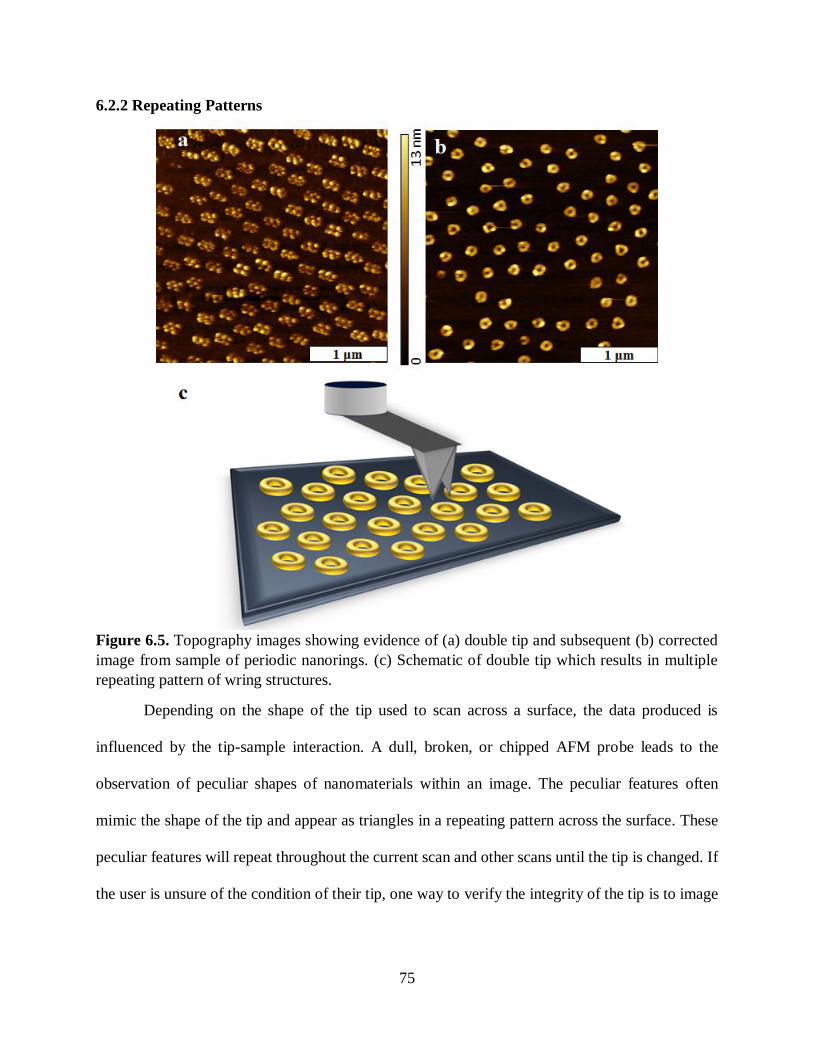
75
6.2.2 Repeating Patterns
Figure 6.5. Topography images showing evidence of (a) double tip and subsequent (b) corrected
image from sample of periodic nanorings. (c) Schematic of double tip which results in multiple
repeating pattern of wring structures.
Depending on the shape of the tip used to scan across a surface, the data produced is
influenced by the tip-sample interaction. A dull, broken, or chipped AFM probe leads to the
observation of peculiar shapes of nanomaterials within an image. The peculiar features often
mimic the shape of the tip and appear as triangles in a repeating pattern across the surface. These
peculiar features will repeat throughout the current scan and other scans until the tip is changed. If
the user is unsure of the condition of their tip, one way to verify the integrity of the tip is to image

76
a sample with a known topography. If the image produces the peculiar shapes, the tip is broken. If
the image exhibits the correct topography, the tip is still usable.
Double tip effect is an AFM tip artifact that occurs when a surface is scanned by a probe
that contains slightly separated protrusions. These separate tip protrusions result in duplicates of
the same feature: true image and the “ghost” image.167,158 Double tips typically come from a
damaged AFM tip that often results in the formation of additional spikes by dislodging particles
during manufacturing, tip use, and through the attachment of surface debris, that often occurs while
imaging.3,168 Published reports on double tip effects explains that collection of dust and debris on
the AFM tip due to long term storage or the AFM tip itself picking up particles on the surface
during repeated scanning can alter the tip shape resulting in a double tip morphology.169 Two
consecutive scans caused by the two tip asperities, as shown in Figure 6.5c, create repetition of the
features in the scan region (Figure 6.5a). A topography image of OTS nanorings on Si(111)
substrate acquired by tapping mode is shown in Figure 6.5a. In this image, the number of nanorings
present in the imaging frame has increased two-fold and the true image of each nanoring has
overlapped with the ghost image as induced by double tip effect. The relative positions of the two
copies is determined by the horizontal separation of two tips. If the horizontal distance between
two tips is relatively smaller than the diameter of the surface feature being imaged, the second
protrusion will begin to trace the feature while the first protrusion reaches the end of the object.169
This causes overlap between real image and ghost image as shown in Figure 6.5a.
The simplest way to avoid double tip artifacts is to recognize the replication of the
same feature in the image and replace the altered tip with a higher quality new tip and rescan the
sample. The tapping mode topography image acquired through rescan using a new tip shows the
true morphology of OTS nanorings (Figure 6.5b) by accurately tracing the object features. In some
77
cases, if the true morphology of the surface features is unknown, the identification of real image
from the ghost image can be uncertain. Several studies have reported novel methods to elucidate
and correct double tip artifacts. Mathematical models have been generated to characterize double
tip effect on cell culture and DNA molecular imaging. The designed mathematical models can be
applied to identify pairs of true and ghost images of spheres and linear molecules in AFM imaging
of unknown samples. 170 Furthermore, Y. F Wang et al developed a “de-blur” technique based on
Bayesian blind deconvolution algorithms to remove double tip artifacts from AFM images
revealing true AFM images with a higher resolution. 171
In Figure 6.6 topography (6.6a) and lateral force (6.6b) images reflect nanoholes in an OTS
matrix that are imaged with a broken or contaminated tip. In the previous Figure 6.5a the double
tip was clearly distinguished by the presence of the “ghost” image of the surface feature that was
observed across the surface. This specific artifact is less distinguishable in Figure 6.5, but when
examined closely the image appears to be out-of-focus and this artifact can be confirmed and
observed more clearly in Figure 6.6b. With a close inspection the appearance of double layered
edge effects can be observed in the OTS buildup around the periphery of the nanopores. This out
of focus artifact typically signifies a slightly damaged tip or possible contamination.

78
Figure 6.6. (A) Topography view of OTS pore imaged with a broken and contaminated tip. This
typically produces images with multiple repeating patterns or an “out-of-focus” appearance
observed in the top image. The corresponding (B) lateral force image contains signs of repeating
patterns.
As discussed above, the common solution for tip contamination or damage is to replace the
tip and reimage the sample. This will help to confirm the state of the previous tip and the actual
morphology of the surface features. Some procedures have been previously described that can be
used to clean the tip so that it may be used again.172 However, this adds additional time and effort
and is not always the most effective route.

79
Figure 6.7. AFM images of spherical nanoparticles imaged with broken tip. (a) Topography
image, 2 x 2 μm2; and corresponding (b) phase image of multiple tip artifact. Corrected (c)
topography and (d) phase image of same nanoparticles imaged with an undamaged tip.
In Figure 6.7, spherical nanoparticles were imaged using tapping mode in ambient
conditions. The triangle shape that is reoccurring in Figure 6.7a is due to a broken tip. A
combination of artifacts occur in this image as the broken tip has resulted in multiple repeating
patterns that likely represent the geometry of the tip as well as the multiple tip sites interacting
with the surface throughout the scan. Although the spherical nanoparticles are present and still
discernable within the image, they are overshadowed by the deformed tip artifact.

80
When an artifact of this caliber is observed, the most effective solution is to change the tip
and re-characterize your sample. In Figure 6.7c and 6.7d images of the sample are shown after the
tip has been replaced. The topography and phase image no longer contain the repeating triangular
pattern observed previously and the spherical nanoparticles true shape is more accurately traced.
6.3 Scanner Artifacts
Piezoelectric scanners are one of the key technologies that made nanoscale imaging
instruments like scanning probe microscopy possible. Within a given AFM system the most
common set-up incorporates a piezoelectric ceramic tube scanner. By applying a voltage to this
material, one can produce a repeatable mechanical response, specifically its change in dimensions.
However, due to their mechanical properties, these piezoelectric materials also introduce artifacts
that can be observed while imaging. When using piezoelectric materials, know that periodic
calibrations are necessary because they to mitigate effects that arise from periods of light or no
use. If the scanner is used often its response can typically be improved. Mitigating the effects of
artifacts induced from scanners can often prove to be more complicated than many artifacts that
are induced by the tip. Image processing software packages are typically how many scanner related
artifacts are corrected.
6.3.1 Scanner Creep
Piezo-ceramics are materials that expand and contract when exposed to voltage gradients.
Both the bias applied to the scanner and the subsequent deformation of the material can be finely
controlled and it is this mechanical property that makes piezo-ceramic materials an ideal candidate
for high resolution 3-D positioning devices. However, when the driving voltage is changed rapidly,
the manner in which the piezo-ceramic material responds is not proportionate in real-time. The
material begins to deform through contraction or expansion but the actual and total position of the

81
tip does not complete its shift at the same time that the voltage is varied. While imaging, this
artifact can most often be observed when the user zooms in our out to gather an image of an area.
When a new area is selected, or a known area is selected to zoom in on, a voltage is applied
to the scanner and the tip is moved through a multi-step mechanism where the initial movement
occurs instantaneously but the later step does not.158 This second step occurs on a longer time
frame and is in the direction of the first change to the driving bias. This is most commonly observed
as a blurring at the beginning of the images in the first few lines of a scan as is shown in Figure
6.8a. The topography images (top row) in Figure 6.8 show an image of CMPS structures on a
surface within an OTS matrix. At the top of Figure 6.8a there is a distortion of the structures that
is the result of scanner creep. This same distortion can be observed in both topography and phase
(Figure 6.8c) because this piezoelectric creep occurs in the x-y piezo-ceramic. This artifact is also
often referred to as “scanner drift” in some texts and should not be confused with the artifact known
as thermal drift.
Figures 6.8b and 6.8d depict the corrected scans of this surface. To correct for scanner
creep, the user must simply wait for the piezo-material to complete its movement and fully
stabilize. It is typical to move to a new area, begin the scan and observe this creep and subsequently
re-scan the same area to obtain the artifact free image.

82
Figure 6.8. Images showing piezo creep artifact and subsequent corrected scan. (A) Topography
view, 2 x 2 μm2; and simultaneously acquired (B) phase image showing evidence of piezo creep
artifact at the early stage of image acquisition. Corrected (C) topography and (D) phase image of
the same area with no evidence of piezo creep.
Scanner creep is not limited to the x-y piezo-positioning components of the scanner. A
similar effect can be observed in the z-direction of topographical channels of data where surface
features with large or steep vertical dimensions. This results in the appearance of very sharp
features in the topograph, but a cursor profile would reveal that there is an overshoot at the leading
and sometimes trailing edges of these traces where the structures would appear taller or deeper at
the edges.
This artifact is illustrated in Figure 6.9 where an overshoot of the tip can be observed in
the cursor trace of the image. The artifact is observed at the beginning and end of sharp features
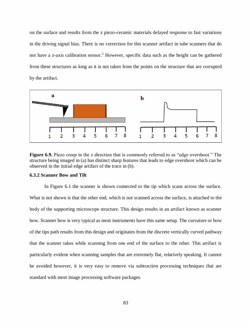
83
on the surface and results from the z piezo-ceramic materials delayed response to fast variations
in the driving signal bias. There is no correction for this scanner artifact in tube scanners that do
not have a z-axis calibration sensor.3 However, specific data such as the height can be gathered
from these structures as long as it is not taken from the points on the structure that are corrupted
by the artifact.
Figure 6.9. Piezo creep in the z direction that is commonly referred to as “edge overshoot.” The
structure being imaged in (a) has distinct sharp features that leads to edge overshoot which can be
observed in the initial edge artifact of the trace in (b).
6.3.2 Scanner Bow and Tilt
In Figure 6.1 the scanner is shown connected to the tip which scans across the surface.
What is not shown is that the other end, which is not scanned across the surface, is attached to the
body of the supporting microscope structure. This design results in an artifact known as scanner
bow. Scanner bow is very typical as most instruments have this same setup. The curvature or bow
of the tips path results from this design and originates from the discrete vertically curved pathway
that the scanner takes while scanning from one end of the surface to the other. This artifact is
particularly evident when scanning samples that are extremely flat, relatively speaking. It cannot
be avoided however, it is very easy to remove via subtraction processing techniques that are
standard with most image processing software packages.

84
Figure 6.10 contains topography images and corresponding cursor profiles of a surface of
porphyrin nanostructures generated via particle lithography. The top row contains a topography
image (Figure 6.10a) and cursor profile (Figure 6.10b) of the surface and nanostructures before
the data has been processed. Evidence of the artifact is seen at the edges and middle of the
topography image as the edges appear darker and the center appears lighter indicating an
unexpected change in surface height when scanner bow is not accounted for. The cursor profile in
Figure 6.10b allows a closer inspection of the degree and presence of the scanner bow. The total
magnitude of the bow spans roughly 10 nanometers. As stated before, this artifact is unavoidable
and mist be corrected post-imaging. The effect does appear less when smaller areas are imaged.
Corrected images are shown in Figure 6.1c and Figure 6.1d. These images were processed and the
background bow was corrected by applying a 2nd order polynomial leveling function tool. The data
is fit by the polynomial of a selectable order and then this fit data is then subtracted to generate a
“level” view of the imaged data. After this subtraction is completed the topography image in Figure
6.10c no longer shows signs of scanner bow and the corresponding cursor profile of the line traced
in the topography image confirms this.
Scanner tilt artifacts have a similar appearance to scanner bow artifacts. Scanner bow
artifacts present as a curved surface while scanner tilt artifacts appear as a slanted or tilted surface.
The explanation for this artifact is quite simple, the sample stage is titled relative to path of the
scanner. Efforts to mount the stage in the most planar sense can be made to reduce this artifact.
Ultimately, the process of a plane or level subtraction will be necessary to remove this artifact,
similar to the processing technique used for scanner bow.

85
Figure 6.10. Topography images depicting the effect of scanner bow before (top row) and after
(bottom row) processing. Two accompanying cursor profiles, before (b) and after (d), match the
lines traced in (a) and (c) and provide a closer look at the “bow” of the scanner’s path as it moves
across the surface/
In Figure 6.11 an image of an unprocessed (Figure 6.11a) topograph and (6.11b) cursor
profile show features of a tilted surface where the sample surface at the top left appears lower than
the bottom right. This artifact is easy to recognize and as easily accounted for. Most imaging
software packages will correct for this while scanning the surface. However, when extracting the
raw data file and moving it another unit, image processing will be necessary to correct for this tilt.
The effects of this correction are displayed in the bottom row of Figure 6.11. Figure 6.11c is a
processed view of the same topography image seen in Figure 6.11a. The tilt has been subtracted
out via a plane subtraction and the corresponding cursor profile in Figure 6.11d reveals that there

86
is no longer an underlying tilt of the surface allowing for a more accurate depiction of the nanoscale
surface facets and features.
Figure 6.11. AFM topography images and cursor profiles that contain scanner tilt artifact. (a)
Topography images of samples before processing that has scanner tilt artifact. (b) Corresponding
cursor profile that traces line observed in (a) that provides view of substrate tilt. Corrected (c)
topography image where the artifact has been processed out and the accompanying (d) cursor
profile.
6.4 Image Processing and Externally Induced Artifacts
All measurements are subject to artifacts and many of these can be prevented and corrected
for given the user understands the sample and the measurement tool as well as what to look for.

87
Image processing occurs after the data has been acquired and is necessary to remove unavoidable
artifacts that are in part due to the design of the system and in part to the scale at which these
measurements are being made. Image processing software packages range in number but all tend
to serve essential key functions that include, data leveling, polynomial and plane corrections
(subtractions), scar corrections that arise from common scanning error (local fault of closed loop),
matrix filtering and 3-D representations of data.158 Typically one or more of these processing tools
will be necessary to appropriately process the images and the data specific to the features of
interest. As noted above, the most common AFM instrument design results in scanner bow and tilt
artifacts for almost all images which would require image processing for every image obtained.
Without the proper knowledge of their specific functions, processing tools could lead to both
complications of the existing artifacts and introduce new ones. Over-processing an image can
result in the loss of data and the dulling of surface features that can ultimately diminish the quality
of your surface image.
Each mode of imaging requires a general understanding of the operational principles to
accurately and effectively manage the imaging parameters to gather the highest quality image of a
given surface. The most common choice includes contact mode where the feedback is managed
via a deflection set-point and tapping mode where the feedback is monitored through an amplitude
set-point and dampening of that signal. The determination of the set points, scan speed, and the
integral and proportional gains will all affect the quality of the image and when incorrectly set can
result in the occurrence of image artifacts. Typically these parameters are determined on a case by
case basis where experimentation with these parameters will result in the optimal settings for that
surface and scan.

88
6.4.1 Image Processing Artifacts and Noise
Figure 6.12 6 x 6 μm2 topograph views of (A) processing artifact and (B) image of the same area
processed correctly.
The user should understand the procedure for image processing thoroughly because it can
help to avoid a majority of common artifacts. It is imperative because one can easily over process
an image by following a procedure line by line and it is possible an image may not need as many
of the processing steps other images may need. It is vital to process an AFM image before
analyzing the image or publishing. To alleviate image processing artifacts, it is advisable to
calibrate the instrument before use. By calibrating the scanner, this will ensure that artifacts that
arise from piezo-ceramic nonlinearities will be reduced during imaging. Nonlinearities are
exemplified by tilt and bow artifacts in an image. Nonlinearities in the scanner may result in a
necessary polynomial background correction that was discussed in detail in the previous section.
Based on the nonlinearities, specific corrections can cause artifacts that lead to a shade-like pattern
that can be observed in Figure 6.12a. In Figure 6.12a, the shade-like pattern alternates on and off
throughout the image. To correct this error, image flattening or leveling is used. This allows the
user to exclude areas that may have a deep nanopore or a tall abnormal structure on the surface.

89
When excluding an area, it omits the undesirable areas in the calculation of the background in the
image leaving the desired image.
Figure 6.13. Electronic noise and processing artifacts in topography images of OTS rings. (a)
Unprocessed topography image that contains evidence of electronic noise. (b) Processed
topography image from (a) that contains processing artifact and electronic noise in the background.
(c) Topography image that has been re-processed with correct masking technique to account for
line defects and (d) new topography image of the surface features where artifacts are no longer
observable.
Processing artifacts can often result after applying corrections in an incorrect order or
without masking specific areas to remove them from the correction process entirely. In Figure
6.13a there are several observable artifacts including, scanner tilt, and electronic noise that are
immediately visible. Some matrix filters, i.e. smoothing, are capable of reducing this electronic
90
noise however they will ultimately dull the sharper features of the surface. A plane correction and
line correction results in the processing artifacts that are observable in Figure 6.13b. The two large
streaks in 6.13b are the result of the extensive corrections that are applied to correct for the sample
tilt and local defects present in the image. This correction without prior masking resulted in the
dark divot effects that can be observed on both sides of the ring. In the proper order, the plane
subtraction is done and an appropriate threshold mask is placed to mask the features of the ring;
finally the local defect correction can be applied and the new topography image in 6.13c is
obtained. This new topography image no longer shows the processing artifact. As previously
discussed, the electronic noise can be partially corrected for by a matrix filter for noise, but in this
case this tool was too detrimental to the OTS ring features so it could not be applied. To remove
this artifact, a grounding wire was placed in contact with the stage and two wires connecting the
controller to the instrument were separated and taped to the floating table. The surface was re-
imaged and the topography image in Figure 6.13d was obtained where no electronic noise was
observed.
6.4.2 Feedback Parameters Artifacts
Optimization of the instrument’s system parameters is essential when obtaining high
quality images for publication. Several parameters must be optimized including scan speed,
proportional and integral-derivative gains (PID), as well as the driving set point. Through a process
of trial-and-error these parameters must be optimized when one begins imaging a new surface. If
the parameters are not optimized then artifacts will appear in the images obtained. These artifacts
occur because when the parameters are not optimized the tip does not accurately trace the surface.
There are generalizations that can be understood to help efficiently optimize these parameters but

91
typically the user will need to fine tune the specifics of these parameters during each imaging
session.
Figure 6.14. Images of “flying tip” artifact observed while characterizing sample of patterned
CMPS. (A) Topography image, 3 x 3 μm2; and (B) corresponding phase image showing CMPS
nanopillars with long tails or “tips”. (C) Corrected topography image of same area with
corresponding (D) phase image in which the tails are no longer observed.
In Figure 6.14 the topography and phase images in the left column contain an artifact that
is commonly referred to as “flying tip”. In the forward trace topography image (Figure 6.14a) there
are tail features that drag to the right of the periodically patterned CMPS nanopillars. This artifact
can often be seen more clearly in the phase image (Figure 6.14c). This artifact can be commonly
observed when imaging tall structures with steep features. Depending on the type of sample and

92
the initial scan rate, typically reducing the amplitude set point (in tapping-mode) and increasing
the integral and proportional gains will force the tip to more accurately track the surface without
deforming the morphology of the nanostructure. Figure 6.14a is a topography image the same
sample surface with the imaging parameters optimized, and the amplitude set point decreased.
After these optimizations the structure tails are no longer present in the image. This can also be
observed in the corresponding phase image (6.14d).
In AFM an electronic controller receives data from the position sensitive photodetector and
compares this measured signal to the driving signal that is set by the user. The difference between
the measured signal and the driving signal is referred to as an error signal. The error signal in a
typical AFM instrument is managed through a PID controller and this is called feedback control.
The PID gains (Proportionate, and Integral-Derivative) must be optimized to obtain an image that
is free of artifacts. The proportionate gain setting helps maintain the probe as it traces smaller
features on the surface and the integral gains are responsible for assisting the probe’s response as
it tracks larger surface features.
In Figure 6.15 there is a topography (Figure 6.15a) and phase (6.15b) image of a single
porphyrin nanopillar on a surface. In an effort to gain high quality images the PID parameters are
often pushed as high as possible to ensure that the tip is reacting as fast as possible to changes in
surface topography. However, imaging steep features at high gains can sometimes result in tip
artifacts that result from systemic oscillations induced by the gains.158 In Figure 6.15a and 6.15b
these oscillations can be observed on the tops of the pillar structures. They can occur often when
zoomed in to small areas that contains structures with sharp morphologies. To reduce the presence
of the artifacts, the gains should be decreased and further optimization of PID gains should be
conducted.

93
Figure 6.15. High resolution image of porphyrin nanopillars with localized systemic oscillation
artifact. (a) Topography image of individual nanopillar with signs of artifact and simultaneously
acquired (b) phase image where oscillation artifacts are more easily observed.
6.5 Conclusions
The artifacts discussed here represent only a few of the many artifacts that can be
commonly encountered when using AFM. These artifacts and many like them derive from discrete
sources within the measuring instrument and measurement analysis. Once one is familiarized with
the nature of these artifacts, they can be more readily observed and corrected.
94
CHAPTER 7. CONCLUSIONS AND FUTURE PROSPECTUS
7.1 Conclusions
High resolution atomic force microscopy (AFM) was applied to analyze and gather
measurements of nanopatterned samples using particle lithography. Platforms of organosilane
nanoholes were fabricated via particle lithography to serve as nano-containers for the generation
of CMPS and porphyrin nanostructures. This fundamental design principle can be used to engineer
an array of nanopatterned, chemically modified, multi-faceted surfaces with controlled
morphological and spatial properties. These nanoscale arrays have potential applications in
molecular electronics, organic photovoltaics, and biosensors.
In Chapter 3 nanopillars of CMPS were generated through nanoholes of OTS. Their growth
and morphology was studied in selected solvents of, bicyclohexane, toluene and dichloromethane.
After characterizing ex situ, these samples with tapping mode AFM, it was concluded that
multilayer structures were formed in all three, but more significant growth was experienced
solutions of toluene and bicyclohexane. Multi-domain pillars were formed more frequently in
solutions of toluene due to solvent integration within the CMPS nanopillars during the
nanostructure formation. CMPS nanopillar growth was also studied at selected temperatures to
gain insight into the molecular assembly mechanism kinetics at lower temperatures. The results
indicate that structures formed at lower temperatures experienced less growth. This data indicates
the significance of the preparation parameters and the control that can be used to fabricate
structures of selectable morphology and composition.
Nanopatterns of CMPS nanopillars were fabricated within an OTS resist layer. This
nanoscale array was used to assemble pyridal porphyrin to surfaces of Si(111) via CMPS
nanopillar foundations. The resulting heterostructures were confirmed via significant height

95
changes after the porphyrin addition step. In total this fabrication scheme required three
independent reactions to fabricate spatially confined CMPS-porphyrin heterostructures. Chapter
5 is a summary of the investigation of a silane-porphyrin coupling reaction that is applied with
particle lithography and techniques of immersion deposition to engineer nanoscale arrays of silicon
porphyrin nanostructures. Through this coupling reaction, silicon porphyrin nanostructures can be
fabricated through a single reaction system with high throughput, tailorable dimensions and
morphology. This strategy offers new novel potential for porphyrin supramolecular assembly on
any surface that furnishes available hydroxyl groups and breaks new ground for surface
modification applications. Future directions for this research include studying the relationship that
nanoscopic volumes of water on the surface play in the exact nanostructure assembly.
In Chapter six commonly encountered imaging artifacts that occur when analyzing surfaces
with an atomic force microscope. The function of this chapter was to provide keen insight from
real sample, imaging, processing, environmental, and systemic artifacts to guide future users
through technique development and to boost efficient capabilities in recognizing error and
correcting for them. This review is comprised of a variety of surfaces and studies that provides a
real snapshot of atomic force microscopies potential application while also discussing the most
effective paths to acquire high resolution and quality data.
7.1 Future Directions
In future, studies, we would like to apply the silane-coupling reaction to a larger set of
porphyrin and phthalocyanine molecules to study their assembly on surfaces of ITO. Through this
method of nanofabrication, precise control of the organization of the potentially electron donating
porphyrin or phthalocyanine can be achieved. The ultimate goal would be to characterize these
nanostructures with photocurrent sensing AFM.

96
Recent studies within our group have incorporated a home-built AFM sample stage for
measuring photocurrents. This stage incorporates a fiber optic cable for transmitting
monochromatic or white light from a solar simulator under an AM 1.5 filter. With the
photoconductive AFM stage, samples can be studied with or without an applied bias while the
temperature of the sample can be monitored through an attached thermocouple. Engineering
surfaces of ITO with nanoscale arrays of silicon-porphyrin and silicon-phthalocyanine
nanostructures could be potentially advantageous in the future development of low cost, high
efficiency organic photovoltaic solar cells. By applying the nanoscale lithography techniques that
were shown throughout this dissertation, we can fabricate porphyrin and phthalocyanine
nanostructures of selectable size and shape. These variations in morphology can be sensitively
probed to study how changes in supramolecular self-assembly can impact the nanostructure’s
photoconductive properties. The self-assembly of porphyrin and phthalocyanine molecules with
varied substituents and band gap properties can be studied ex-situ with current prototypes in the
lab. Future work would also seek to expand the scope of these investigations to include in-situ
AFM analysis of the various porphyrin film and nanostructure growth in real time.

97
REFERENCES
1. Kanaizuka, K.; Izumi, A.; Ishizaki, M.; Kon, H.; Togashi, T.; Miyake, R.; Ishida, T.;
Tamura, R.; Haga, M.-a.; Moritani, Y.; Sakamoto, M.; Kurihara, M., Molecular nanostamp based
on one-dimensional porphyrin polymers. ACS App. Mat. Interfaces 2013, 5 (15), 6879-6885.
2. Binnig, G.; Quate, C. F.; Gerber, C., Atomic force microscope. Phys. Rev. Lett. 1986, 56
(9), 930-933.
3. Eaton, P.; West, P., Atomic Force Microscopy. Oxford University Press: 2010.
4. Gewirth, A. A.; Niece, B. K., Electrochemical applications of in situ scanning probe
microscopy. Chem. Rev. 1997, 97 (4), 1129-1162.
5. Hamers, R. J., Scanned probe microscopies in chemistry. J. Phys. Chem. 1996, 100 (31),
13103-13120.
6. Alvarez, J.; Ngo, I.; Gueunier-Farret, M.-E.; Kleider, J.-P.; Yu, L.; Cabarrocas, P. R.;
Perraud, S.; Rouvière, E.; Celle, C.; Mouchet, C.; Simonato, J.-P., Conductive-probe atomic
force microscopy characterization of silicon nanowire. Nanoscale Res. Lett. 2011, 6 (1), 110.
7. Houzé, F.; Meyer, R.; Schneegans, O.; Boyer, L., Imaging the local electrical properties
of metal surfaces by atomic force microscopy with conducting probes. Appl Phys Lett 1996, 69.
8. Marohn, J. A.; Fainchtein, R.; Smith, D. D., Mechanical modulation of sample
magnetization in magnetic resonance force microscopy. J. App. Phys. 1999, 86 (8), 4619-4625.
9. Guillermet, O.; Gauthier, S.; Joachim, C.; de Mendoza, P.; Lauterbach, T.; Echavarren,
A., Stm and afm high resolution intramolecular imaging of a single decastarphene molecule.
Chem. Phys. Lett. 2011, 511 (4), 482-485.
10. Binnig, G.; Rohrer, H.; Gerber, C.; Weibel, E., Tunneling through a controllable vacuum
gap. Appl. Phys. Lett. 1982, 40 (2), 178-180.
11. Binnig, G.; Rohrer, H.; Gerber, C.; Weibel, E., 7 \ifmmode\times\else\texttimes\fi{} 7
reconstruction on si(111) resolved in real space. Phys. Rev. Lett. 1983, 50 (2), 120-123.
12. Binnig, G.; Rohrer, H., Scanning tunneling microscopy. Surf. Sci. 1983, 126 (1), 236-
244.
13. Binnig, G.; Ch, G.; Stoll, E.; Albrecht, T. R.; Quate, C. F., Atomic resolution with atomic
force microscope. EPL (Europhysics Letters) 1987, 3 (12), 1281.
14. Shi, Y.; Yan, H.-J.; Wen, R.; Wan, L.-J., Direct visualization of nucleation and growth
processes of solid electrolyte interphase film using in situ atomic force microscopy. ACS App.
Mat. Interfaces 2017.

98
15. Beaulieu, L. Y.; Hatchard, T. D.; Bonakdarpour, A.; Fleischauer, M. D.; Dahn, J. R.,
Reaction of li with alloy thin films studied by in situ AFM. J. Electrochem. Soc. 2003, 150 (11),
A1457-A1464.
16. Garno, J. C.; Amro, N. A.; Wadu-Mesthrige, K.; Liu, G.-Y., Production of periodic
arrays of protein nanostructures using particle lithography. Langmuir 2002, 18 (21), 8186-8192.
17. He, Y.; Ye, T.; Su, M.; Zhang, C.; Ribbe, A. E.; Jiang, W.; Mao, C., Hierarchical self-
assembly of DNA into symmetric supramolecular polyhedra. Nature 2008, 452 (7184), 198-201.
18. Junno, T.; Deppert, K.; Montelius, L.; Samuelson, L., Controlled manipulation of
nanoparticles with an atomic force microscope. Appl. Phys. Lett. 1995, 66 (26), 3627-3629.
19. Kim, S. H.; Opdahl, A.; Marmo, C.; Somorjai, G. A., AFM and SFG studies of phema-
based hydrogel contact lens surfaces in saline solution: Adhesion, friction, and the presence of
non-crosslinked polymer chains at the surface. Biomaterials 2002, 23 (7), 1657-1666.
20. Lee, K.-B.; Lim, J.-H.; Mirkin, C. A., Protein nanostructures formed via direct-write dip-
pen nanolithography. J. Am. Chem. Soc. 2003, 125 (19), 5588-5589.
21. Manne, S.; Butt, H. J.; Gould, S. A. C.; Hansma, P. K., Imaging metal atoms in air and
water using the atomic force microscope. Appl. Phys. Lett. 1990, 56 (18), 1758-1759.
22. Talley, C. E.; Jackson, J. B.; Oubre, C.; Grady, N. K.; Hollars, C. W.; Lane, S. M.; Huser,
T. R.; Nordlander, P.; Halas, N. J., Surface-enhanced raman scattering from individual au
nanoparticles and nanoparticle dimer substrates. Nano Letters 2005, 5 (8), 1569-1574.
23. Ton-That, C.; Shard, A. G.; Teare, D. O. H.; Bradley, R. H., Xps and afm surface studies
of solvent-cast ps/pmma blends. Polymer 2001, 42 (3), 1121-1129.
24. Zheng, J.; Li, Z.; Wu, A.; Zhou, H., Afm studies of DNA structures on mica in the
presence of alkaline earth metal ions. Biophys. Chem. 2003, 104 (1), 37-43.
25. Alexeev, A.; Loos, J.; Koetse, M. M., Nanoscale electrical characterization of
semiconducting polymer blends by conductive atomic force microscopy (c-afm).
Ultramicroscopy 2006, 106 (3), 191-199.
26. Bridger, P. M.; Bandić, Z. Z.; Piquette, E. C.; McGill, T. C., Measurement of induced
surface charges, contact potentials, and surface states in gan by electric force microscopy. Appl.
Phys. Lett. 1999, 74 (23), 3522-3524.
27. Hansma, P. K.; Cleveland, J. P.; Radmacher, M.; Walters, D. A.; Hillner, P. E.; Bezanilla,
M.; Fritz, M.; Vie, D.; Hansma, H. G.; Prater, C. B.; Massie, J.; Fukunaga, L.; Gurley, J.; Elings,
V., Tapping mode atomic force microscopy in liquids. Appl. Phys. Lett. 1994, 64 (13), 1738-
1740.

99
28. Kuwahara, Y., Muscovite surface structure imaged by fluid contact mode afm. Phys.
Chem. Min. 1999, 26 (3), 198-205.
29. Nonnenmacher, M.; O’Boyle, M. P.; Wickramasinghe, H. K., Kelvin probe force
microscopy. Appl. Phys. Lett. 1991, 58 (25), 2921-2923.
30. Pingree, L. S. C.; Reid, O. G.; Ginger, D. S., Imaging the evolution of nanoscale
photocurrent collection and transport networks during annealing of polythiophene/fullerene solar
cells. Nano Letters 2009, 9 (8), 2946-2952.
31. Rugar, D.; Mamin, H. J.; Guethner, P.; Lambert, S. E.; Stern, J. E.; McFadyen, I.; Yogi,
T., Magnetic force microscopy: General principles and application to longitudinal recording
media. J. App. Phys. 1990, 68 (3), 1169-1183.
32. Cappella, B.; Baschieri, P.; Frediani, C.; Miccoli, P.; Ascoli, C., Improvements in afm
imaging of the spatial variation of force - distance curves: On-line images. Nanotechnology
1997, 8 (2), 82.
33. Cappella, B.; Dietler, G., Force-distance curves by atomic force microscopy. Surf. Sci.
Rep. 1999, 34 (1), 1-104.
34. Hugel, T.; Seitz, M., The study of molecular interactions by afm force spectroscopy.
Macromo. Rap. Commun. 2001, 22 (13), 989-1016.
35. Ebenstein, Y.; Nahum, E.; Banin, U., Tapping mode atomic force microscopy for
nanoparticle sizing: Tip−sample interaction effects. Nano Lett. 2002, 2 (9), 945-950.
36. McLean, R. S.; Sauer, B. B., Tapping-mode afm studies using phase detection for
resolution of nanophases in segmented polyurethanes and other block copolymers.
Macromolecules 1997, 30 (26), 8314-8317.
37. Möller, C.; Allen, M.; Elings, V.; Engel, A.; Müller, D. J., Tapping-mode atomic force
microscopy produces faithful high-resolution images of protein surfaces. Biophys. J. 1999, 77
(2), 1150-1158.
38. Zhong, Q.; Inniss, D.; Kjoller, K.; Elings, V. B., Fractured polymer/silica fiber surface
studied by tapping mode atomic force microscopy. Surf. Sci. 1993, 290 (1), L688-L692.
39. Schmitz, I.; Schreiner, M.; Friedbacher, G.; Grasserbauer, M., Phase imaging as an
extension to tapping mode afm for the identification of material properties on humidity-sensitive
surfaces. App. Surf. Sci. 1997, 115 (2), 190-198.
40. Tamayo, J.; García, R., Deformation, contact time, and phase contrast in tapping mode
scanning force microscopy. Langmuir 1996, 12 (18), 4430-4435.

100
41. Leclère, P.; Lazzaroni, R.; Brédas, J. L.; Yu, J. M.; Dubois, P.; Jérôme, R., Microdomain
morphology analysis of block copolymers by atomic force microscopy with phase detection
imaging. Langmuir 1996, 12 (18), 4317-4320.
42. Raghavan, D.; VanLandingham, M.; Gu, X.; Nguyen, T., Characterization of
heterogeneous regions in polymer systems using tapping mode and force mode atomic force
microscopy. Langmuir 2000, 16 (24), 9448-9459.
43. Sagiv, J., Organized monolayers by adsorption. 1. Formation and structure of oleophobic
mixed monolayers on solid surfaces. J. Am. Chem. Soc. 1980, 102 (1), 92-98.
44. Li, J. R.; Garno, J. C., Elucidating the role of surface hydrolysis in preparing
organosilane nanostructures via particle lithography. Nano Lett. 2008, 8 (7), 1916-1922.
45. Duchet, J.; Chabert, B.; Chapel, J. P.; Gérard, J. F.; Chovelon, J. M.; Jaffrezic-Renault,
N., Influence of the deposition process on the structure of grafted alkylsilane layers. Langmuir
1997, 13 (8), 2271-2278.
46. Campbell, I. H.; Kress, J. D.; Martin, R. L.; Smith, D. L.; Barashkov, N. N.; Ferraris, J.
P., Controlling charge injection in organic electronic devices using self-assembled monolayers.
Appl. Phys. Lett. 1997, 71 (24), 3528-3530.
47. Jennings, G. K.; Laibinis, P. E., Self-assembled monolayers of alkanethiols on copper
provide corrosion resistance in aqueous environments. Colloids Surf., A 1996, 116 (1), 105-114.
48. Lee, S.; Shon, Y.-S.; Colorado, R.; Guenard, R. L.; Lee, T. R.; Perry, S. S., The influence
of packing densities and surface order on the frictional properties of alkanethiol self-assembled
monolayers (sams) on gold: A comparison of sams derived from normal and spiroalkanedithiols.
Langmuir 2000, 16 (5), 2220-2224.
49. McDermott, M. T.; Green, J.-B. D.; Porter, M. D., Scanning force microscopic
exploration of the lubrication capabilities of n-alkanethiolate monolayers chemisorbed at gold:
Structural basis of microscopic friction and wear. Langmuir 1997, 13 (9), 2504-2510.
50. Wolkow, R. A., Controlled molecular adsorption on silicon: Laying a foundation for
molecular devices. Annu. Rev. Phys. Chem. 1999, 50 (1), 413-441.
51. Zamborini, F. P.; Crooks, R. M., Corrosion passivation of gold by n-alkanethiol self-
assembled monolayers: Effect of chain length and end group. Langmuir 1998, 14 (12), 3279-
3286.
52. Le Grange, J. D.; Markham, J. L.; Kurkjian, C. R., Effects of surface hydration on the
deposition of silane monolayers on silica. Langmuir 1993, 9 (7), 1749-1753.
53. McGovern, M. E.; Kallury, K. M. R.; Thompson, M., Role of solvent on the silanization
of glass with octadecyltrichlorosilane. Langmuir 1994, 10 (10), 3607-3614.

101
54. Ulman, A., Formation and structure of self-assembled monolayers. Chem. Rev. 1996, 96
(4), 1533-1554.
55. Schreiber, F., Structure and growth of self-assembling monolayers. Prog. Surf. Sci. 2000,
65 (5-8), 151-256.
56. Poirier, G. E.; Pylant, E. D., The self-assembly mechanism of alkanethiols on au(111).
Science 1996, 272 (5265), 1145-1148.
57. Wen, K.; Maoz, R.; Cohen, H.; Sagiv, J.; Gibaud, A.; Desert, A.; Ocko, B. M.,
Postassembly chemical modification of a highly ordered organosilane multilayer: New insights
into the structure, bonding, and dynamics of self-assembling silane monolayers. ACS Nano 2008,
2 (3), 579-599.
58. Grabar, K. C.; Allison, K. J.; Baker, B. E.; Bright, R. M.; Brown, K. R.; Freeman, R. G.;
Fox, A. P.; Keating, C. D.; Musick, M. D.; Natan, M. J., Two-dimensional arrays of colloidal
gold particles: A flexible approach to macroscopic metal surfaces. Langmuir 1996, 12 (10),
2353-2361.
59. Chrisey, L. A.; Lee, G. U.; Oferrall, C. E., Covalent attachment of synthetic DNA to self-
assembled monolayer films. Nucleic Acids Res. 1996, 24 (15), 3031-3039.
60. Mooney, J. F.; Hunt, A. J.; McIntosh, J. R.; Liberko, C. A.; Walba, D. M.; Rogers, C. T.,
Patterning of functional antibodies and other proteins by photolithography of silane monolayers.
Proc. Natl. Acad. Sci. U. S. A. 1996, 93 (22), 12287-12291.
61. Faucheux, N.; Schweiss, R.; Lutzow, K.; Werner, C.; Groth, T., Self-assembled
monolayers with different terminating groups as model substrates for cell adhesion studies.
Biomaterials 2004, 25 (14), 2721-2730.
62. Sagiv, J., Organized monolayers by adsorption .1. Formation and structure of oleophobic
mixed monolayers on solid-surfaces. J. Am. Chem. Soc. 1980, 102 (1), 92-98.
63. Vallant, T.; Kattner, J.; Brunner, H.; Mayer, U.; Hoffmann, H., Investigation of the
formation and structure of self-assembled alkylsiloxane monolayers on silicon using in situ
attenuated total reflection infrared spectroscopy. Langmuir 1999, 15 (16), 5339-5346.
64. Mathauer, K.; Frank, C. W., Binary self-assembled monolayers as prepared by successive
adsorption of alkyltrichlorosilanes. Langmuir 1993, 9 (12), 3446-3451.
65. Grabar, K. C.; Freeman, R. G.; Hommer, M. B.; Natan, M. J., Preparation and
characterization of au colloid monolayers. Anal. Chem. 1995, 67 (4), 735-743.
66. Kurth, D. G.; Bein, T., Thin-films of (3-aminopropyl)triethoxysilane on aluminum-oxide
and gold substrates. Langmuir 1995, 11 (8), 3061-3067.

102
67. Tillman, N.; Ulman, A.; Schildkraut, J. S.; Penner, T. L., Incorporation of phenoxy
groups in self-assembled monolayers of trichlorosilane derivatives - effects on film thickness,
wettability, and molecular-orientation. J. Am. Chem. Soc. 1988, 110 (18), 6136-6144.
68. Koloski, T. S.; Dulcey, C. S.; Haralson, Q. J.; Calvert, J. M., Nucleophilic displacement
reactions at benzyl halide self-assembled monolayer film surfaces. Langmuir 1994, 10 (9), 3122-
3133.
69. Mineo, P.; Motta, A.; Lupo, F.; Renna, L.; Gulino, A., Si(111) surface engineered with
ordered nanostructures by an atom transfer radical polymerization. J. Phys. Chem. C 2011, 115
(25), 12293-12298.
70. Sun, S.; Montague, M.; Critchley, K.; Chen, M.-S.; Dressick, W. J.; Evans, S. D.;
Leggett, G. J., Fabrication of biological nanostructures by scanning near-field photolithography
of chloromethylphenylsiloxane monolayers. Nano Letters 2006, 6 (1), 29-33.
71. Brandow, S. L.; Chen, M. S.; Dulcey, C. S.; Dressick, W. J., Formation of aromatic
siloxane self-assembled monolayers. Langmuir 2008, 24 (8), 3888-3896.
72. Brandow, S. L.; Chen, M.-S.; Fertig, S. J.; Chrisey, L. A.; Dulcey, C. S.; Dressick, W. J.,
Surface patterning of polychloromethylstyrene films. Chemistry – A European Journal 2001, 7
(20), 4495-4499.
73. Dressick, W. J.; Dulcey, C. S.; Brandow, S. L.; Witschi, H.; Neeley, P. F., Proximity x-
ray lithography of siloxane and polymer films containing benzyl chloride functional groups. J. V.
Sci. & Tech.y A: Vacuum, Surfaces, and Films 1999, 17 (4), 1432-1440.
74. Lercel, M. J.; Craighead, H. G.; Parikh, A. N.; Seshadri, K.; Allara, D. L., Sub-10 nm
lithography with self-assembled monolayers. Appl. Phys. Lett. 1996, 68 (11), 1504-1506.
75. Golzhauser, A.; Eck, W.; Geyer, W.; Stadler, V.; Weimann, T.; Hinze, P.; Grunze, M.,
Chemical nanolithography with electron beams. Adv.Mat. 2001, 13 (11), 806-+.
76. Wang, D. W.; Thomas, S. G.; Wang, K. L.; Xia, Y. N.; Whitesides, G. M., Nanometer
scale patterning and pattern transfer on amorphous si, crystalline si, and sio2 surfaces using self-
assembled monolayers. Appl. Phys. Lett. 1997, 70 (12), 1593-1595.
77. Xia, Y.; Mrksich, M.; Kim, E.; Whitesides, G. M., Microcontact printing of
octadecylsiloxane on the surface of silicon dioxide and its application in microfabrication. J. Am.
Chem. Soc. 1995, 117 (37), 9576-9577.
78. Mirkin, C. A.; Hong, S. H.; Demers, L., Dip-pen nanolithography: Controlling surface
architecture on the sub-100 nanometer length scale. ChemPhysChem 2001, 2 (1), 37-39.
103
79. Rosa, L. G.; Jiang, J. Y.; Lima, O. V.; Xiao, J.; Utreras, E.; Dowben, P. A.; Tan, L.,
Selective nanoshaving of self-assembled monolayers of 2-(4-pyridylethyl)triethoxysilane. Mater.
Lett. 2009, 63 (12), 961-964.
80. Headrick, J. E.; Armstrong, M.; Cratty, J.; Hammond, S.; Sheriff, B. A.; Berrie, C. L.,
Nanoscale patterning of alkyl monolayers on silicon using the atomic force microscope.
Langmuir 2005, 21 (9), 4117-4122.
81. Xu, S.; Miller, S.; Laibinis, P. E.; Liu, G. Y., Fabrication of nanometer scale patterns
within self-assembled monolayers by nanografting. Langmuir 1999, 15 (21), 7244-7251.
82. Lee, M. V.; Nelson, K. A.; Hutchins, L.; Becerril, H. A.; Cosby, S. T.; Blood, J. C.;
Wheeler, D. R.; Davis, R. C.; Woolley, A. T.; Harb, J. N.; Linford, M. R., Nanografting of
silanes on silicon dioxide with applications to DNA localization and copper electroless
deposition. Chem. Mat. 2007, 19 (21), 5052-5054.
83. Gu, J. H.; Yam, C. M.; Li, S.; Cai, C. Z., Nanometric protein arrays on protein-resistant
monolayers on silicon surfaces. J. Am. Chem. Soc. 2004, 126 (26), 8098-8099.
84. Deckman, H. W.; Dunsmuir, J. H., Natural lithography. App. Phys. Lett. 1982, 41 (4),
377-379.
85. Chen, T.; Chang, D. P.; Jordan, R.; Zauscher, S., Colloidal lithography for fabricating
patterned polymer-brush microstructures. Beilstein J. Nanotechno. 2012, 3, 397-403.
86. Jiang, P.; Hwang, K. S.; Mittleman, D. M.; Bertone, J. F.; Colvin, V. L., Template-
directed preparation of macroporous polymers with oriented and crystalline arrays of voids. J.
Am. Chem. Soc. 1999, 121 (50), 11630-11637.
87. Taylor, Z. R.; Patel, K.; Spain, T. G.; Keay, J. C.; Jernigen, J. D.; Sanchez, E. S.; Grady,
B. P.; Johnson, M. B.; Schmidtke, D. W., Fabrication of protein dot arrays via particle
lithography. Langmuir 2009, 25 (18), 10932-10938.
88. Agheli, H.; Malmstrom, J.; Larsson, E. M.; Textor, M.; Sutherland, D. S., Large area
protein nanopatterning for biological applications. Nano Letters 2006, 6 (6), 1165-1171.
89. Haynes, C. L.; Van Duyne, R. P., Nanosphere lithography: A versatile nanofabrication
tool for studies of size-dependent nanoparticle optics. J. Phys. Chem. B 2001, 105 (24), 5599-
5611.
90. Zhou, C. M.; Gall, D., Surface patterning by nanosphere lithography for layer growth
with ordered pores. Thin Solid Films 2007, 516 (2-4), 433-437.
91. Lewandowski, B. R.; Kelley, A. T.; Singleton, R.; Li, J. R.; Lowry, M.; Warner, I. M.;
Garno, J. C., Nanostructures of cysteine-coated cds nanoparticles produced with "two-particle"
lithography. J. Phys. Chem. C 2009, 113 (15), 5933-5940.

104
92. Glangchai, L. C.; Caldorera-Moore, M.; Shi, L.; Roy, K., Nanoimprint lithography based
fabrication of shape-specific, enzymatically-triggered smart nanoparticles. J. Control. Release
2008, 125 (3), 263-272.
93. Englade-Franklin, L. E.; Morrison, G.; Verberne-Sutton, S. D.; Francis, A. L.; Chan, J.
Y.; Garno, J. C., Surface-directed synthesis of erbium-doped yttrium oxide nanoparticles within
organosilane zeptoliter containers. ACS App. Mater. Interfaces 2014, 6 (18), 15942-15949.
94. Tian, T.; LeJeune, Z. M.; Garno, J. C., Directed surface assembly of 4-
(chloromethyl)phenyltrichlorosilane: Self-polymerization within spatially confined sites of
si(111) viewed by atomic force microscopy. Langmuir 2013, 29 (22), 6529-6536.
95. Lusker, K. L.; Yu, J. J.; Garno, J. C., Particle lithography with vapor deposition of
organosilanes: A molecular toolkit for studying confined surface reactions in nanoscale liquid
volumes. Thin Solid Films 2011, 519 (15), 5223-5229.
96. Brownfield, A. L.; Causey, C. P.; Mullen, T. J., Influence of solvent on
octadecyltrichlorosilane nanostructures fabricated using particle lithography. J. Phys. Chem. C
2015, 119 (22), 12455-12463.
97. Saner, C. K.; Lusker, K. L.; LeJeune, Z. M.; Serem, W. K.; Garno, J. C., Self-assembly of
octadecyltrichlorosilane: Surface structures formed using different protocols of particle
lithography. Beilstein J. Nanotechnol. 2012, 3, 114-122.
98. Tian, T.; LeJeune, Z. M.; Garno, J. C., Directed surface assembly of 4-
(chloromethyl)phenyltrichlorosilane: Self-polymerization within spatially confined sites of
si(111) viewed by atomic force microscopy. Langmuir 2013, 29, 6529-6536.
99. Rozlosnik, N.; Gerstenberg, M. C.; Larsen, N. B., Effect of solvents and concentration on
the formation of a self-assembled monolayer of octadecylsiloxane on silicon (001). Langmuir
2003, 19 (4), 1182-1188.
100. Vallant, T.; Brunner, H.; Mayer, U.; Hoffmann, H.; Leitner, T.; Resch, R.; Friedbacher,
G., Formation of self-assembled octadecylsiloxane monolayers on mica and silicon surfaces
studied by atomic force microscopy and infrared spectroscopy. J. Phys. Chem. B 1998, 102 (37),
7190-7197.
101. Jeon, N. L.; Finnie, K.; Branshaw, K.; Nuzzo, R. G., Structure and stability of patterned
self-assembled films of octadecyltrichlorosilane formed by contact printing. Langmuir 1997, 13
(13), 3382-3391.
102. Auwarter, W.; Ecija, D.; Klappenberger, F.; Barth, J. V., Porphyrins at interfaces. Nat
Chem 2015, 7 (2), 105-120.

105
103. Li, D.; Swanson, B. I.; Robinson, J. M.; Hoffbauer, M. A., Porphyrin based self-
assembled monolayer thin films: Synthesis and characterization. J. Am. Chem. Soc. 1993, 115
(15), 6975-6980.
104. Li, D.; Buscher, C. T.; Swanson, B. I., Synthesis, characterization, and properties of
covalently bound, self-assembled porphyrin multilayer thin films. Chem. Mat. 1994, 6 (6), 803-
810.
105. Garno, J. C.; Xu, C.; Bazzan, G.; Batteas, J. D.; Drain, C. M., Designing supramolecular
porphyrin arrays for surface assembly and patterning of optoelectronic materials. In Metal-
containing and metallosupramolecular polymers and materials, American Chemical Society:
2006; Vol. 928, pp 168-183.
106. Cai, J.; Chen, H.; Huang, J.; Wang, J.; Tian, D.; Dong, H.; Jiang, L., Controlled self-
assembly and photovoltaic characteristics of porphyrin derivatives on a silicon surface at solid-
liquid interfaces. Soft Matter 2014, 10 (15), 2612-2618.
107. Bai, F.; Sun, Z.; Wu, H.; Haddad, R. E.; Coker, E. N.; Huang, J. Y.; Rodriguez, M. A.;
Fan, H., Porous one-dimensional nanostructures through confined cooperative self-assembly.
Nano Letters 2011, 11 (12), 5196-5200.
108. Miller, J. S., Polymorphic molecular materials—the importance of tertiary structures.
Adv. Mater. 1998, 10 (18), 1553-1557.
109. Alivisatos, P.; Barbara, P. F.; Castleman, A. W.; Chang, J.; Dixon, D. A.; Klein, M. L.;
McLendon, G. L.; Miller, J. S.; Ratner, M. A.; Rossky, P. J.; Stupp, S. I.; Thompson, M. E.,
From molecules to materials: Current trends and future directions. Adv. Mater. 1998, 10 (16),
1297-1336.
110. Senge, M. O.; Fazekas, M.; Notaras, E. G. A.; Blau, W. J.; Zawadzka, M.; Locos, O. B.;
Ni Mhuircheartaigh, E. M., Nonlinear optical properties of porphyrins. Adv. Mater. 2007, 19
(19), 2737-2774.
111. Benítez, I. O.; Bujoli, B.; Camus, L. J.; Lee, C. M.; Odobel, F.; Talham, D. R.,
Monolayers as models for supported catalysts: Zirconium phosphonate films containing
manganese(iii) porphyrins. J. Am. Chem. Soc. 2002, 124 (16), 4363-4370.
112. Zhai, X.; Alexander, D.; Derosa, P.; Garno, J. C., Distance-dependent measurements of
the conductance of porphyrin nanorods studied with conductive probe atomic force microscopy.
Langmuir 2017, 33 (5), 1132-1138.
113. Zhai, X.; Arachchige, N. M. K. K.; Derosa, P.; Garno, J. C., Conductive-probe
measurements with nanodots of free-base and metallated porphyrins. J. Colloid Interface Sci.
2017, 486, 38-45.

106
114. Lepper, M.; Kobl, J.; Schmitt, T.; Gurrath, M.; deSiervo, A.; Schneider, M. A.; Steinruck,
H.-P.; Meyer, B.; Marbach, H.; Hieringer, W., ‘‘Inverted’’ porphyrins: A distorted adsorption
geometry of free-base porphyrins on cu(111). Chem. Commun. 2017, 53, 8207.
115. Albrecht, F.; Bischoff, F.; Auwarter, W.; Barth, J. V.; Repp, J., Direct identification and
determination of conformational response in adsorbed individual nonplanar molecular species
using noncontact atomic force microscopy. Nano Lett. 2016, 16, 7703-7709.
116. Lu, X.; Hipps, K. W.; Wang, X. D.; Mazur, U., Scanning tunneling microscopy of metal
phthalocyanines: D7 and d9 cases. J. Am. Chem. Soc, 1996, 118, 7197-7202.
117. Lei, S.-B.; Deng, K.; Yan-Lian, Y.; Zeng, Q.-D.; Wang, C.; Jiang, J.-Z., Electric driven
molecular switching of asymmetric tris(phthalocyaninato) lutetium triple-decker complex at the
liquid/solid interface. Nano Lett. 2008, 8, 1836-1843.
118. Bearinger, J. P.; Stone, G.; Christian, A. T.; Dugan, L.; Hiddessen, A. L.; Wu, K. J.; Wu,
L.; Hamilton, J.; Stockton, C.; Hubbell, J. A., Porphyrin-based photocatalytic lithography.
Langmuir 2008, 24, 5179-5184.
119. Bearinger, J. P.; Stone, G.; Dugan, L. C.; ElDasher, B.; Stockton, C.; Conway, J. W.;
Kuenzler, T.; Hubbell, J. A., Porphyrin-based photocatalytic nanolithography: A new fabrication
tool for protein arrays. Molec. Cell. Proteomics 2009, 8, 1823-1831.
120. Vesper, B. J.; Salaita, K.; Zong, H.; Mirking, C. A.; Barrett, A. G. M.; Hoffman, B. M.,
Surface-bound porphyrazines: Controlling reduction potentials of self-assembled monolayers
through molecular proximity/orientation to a metal surface. J. Am. Chem. Soc, 2004, 126, 16653-
16658.
121. Chen, X.; Lei, S.; Lotze, C.; Czekelius, C.; Paulus, B.; Franke, K. J., Conformational
adaptation and manipulation of manganese tetra(4-pyridyl)porphyrin molecules on cu(111). J.
Chem. Phys, 2017, 146, 092316.
122. Samori, P.; Engelkamp, H.; deWitte, P. A. J.; Rowan, A. E.; Nolte, R. J. M.; Rabe, J. P.,
Self-organization of semiconducting polysiloxane-phthalocyanine on a graphite surface. Adv.
Mater. 2005, 17, 1265-1268.
123. Shimadzu, T.; Segawa, H.; Wu, F.; Nakayama, N., Approaches to conducting polymer
devices with nanostructures: Photoelectrochemical function of one-dimensional and two-
dimensional porphyrin polymers with oligothienyl molecular wire. J. Photochem. Photobiol. A
1995, 92, 121-127.
124. Holten, D.; Bocian, D. F.; Lindsey, J. S., Probing electronic communication in covalently
linked multiporphyrin arrays. A guide to the rational design of molecular photonic devices. Acc.
Chem. Res. 2001, 35, 57-69.

107
125. Saner, C. K.; Lu, L.; Zhang, D.; Garno, J. C., Chemical approaches for nanoscale
patterning based on particle lithography with proteins and organic thin films. Nanotechnol. Rev.
2015, 4, 129-143.
126. Hulteen, J. C.; Duyne, R. P. V., Nanosphere lithography: A materials general fabrication
process for periodic particle array surfaces. Journal of Vacuum Science & Technology A:
Vacuum, Surfaces, and Films 1995, 13 (3), 1553-1558.
127. Bae, C.; Shin, H.; Moon, J.; Sung, M. M., Contact area lithography (cal): A new
approach to direct formation of nanometric chemical patterns. Chem. Mat. 2006, 18 (5), 1085-
1088.
128. Jensen, T. R.; Malinsky, M. D.; Haynes, C. L.; Van Duyne, R. P., Nanosphere
lithography: Tunable localized surface plasmon resonance spectra of silver nanoparticles. J. of
Phys. Chem. B 2000, 104 (45), 10549-10556.
129. Haynes, C. L.; Van Duyne, R. P., Nanosphere lithography: A versatile nanofabrication
tool for studies of size-dependent nanoparticle optics. J. Phys. Chem. B 2001, 105 (24), 5599-
5611.
130. Chen, J.; Liao, W.-S.; Chen, X.; Yang, T.; Wark, S. E.; Son, D. H.; Batteas, J. D.;
Cremer, P. S., Evaporation-induced assembly of quantum dots into nanorings. ACS Nano 2009, 3
(1), 173-180.
131. Chen, M. S.; Brandow, S. L.; Schull, T. L.; Chrisey, D. B.; Dressick, W. J., A non-
covalent approach for depositing spatially selective materials on surfaces. Adv. Funct.
Mater.2005, 15 (8), 1364-1375.
132. Brandow, S. L.; Chen, M.-S.; Dulcey, C. S.; Dressick, W. J., Formation of aromatic
siloxane self-assembled monolayers. Langmuir 2008, 24 (8), 3888-3896.
133. Chambers, P. C.; Garno, J. C., Surface self-assembly of 4-
(chloromethyl)phenyltrichlorosilane studied with selected solvents and temperatures. Thin Solid
Films 2017, submitted.
134. Nečas, D.; Klapetek, P., Gwyddion: An open-source software for spm data analysis.
Central European Journal of Physics 2012, 10 (1), 181-188.
135. Cai, J.; Chen, H.; Huang, J.; Wang, J.; Tian, D.; Dong, H.; Jiang, L., Controlled self-
assembly and photovoltaic characteristics of porphyrin derivatives on a silicon surface at solid-
liquid interfaces. Soft Matter 2014, 10 (15), 2612-8.
136. Galstyan, A.; Kauscher, U.; Block, D.; Ravoo, B. J.; Strassert, C. A., Silicon(iv)
phthalocyanine-decorated cyclodextrin vesicles as a self-assembled phototherapeutic agent
against mrsa. ACS App. Mater. Interfaces 2016, 8 (20), 12631-12637.

108
137. Zysman-Colman, E.; Ghosh, S. S.; Xie, G.; Varghese, S.; Chowdhury, M.; Sharma, N.;
Cordes, D. B.; Slawin, A. M. Z.; Samuel, I. D. W., Solution-processable silicon phthalocyanines
in electroluminescent and photovoltaic devices. ACS App. Mater. Interfaces 2016, 8 (14), 9247-
9253.
138. Brinker, C. J.; Lu, Y.; Sellinger, A.; Fan, H., Evaporation-induced self-assembly:
Nanostructures made easy. Adv. Mater. 1999, 11 (7), 579-585.
139. Chen, Y.; Li, A.; Huang, Z.-H.; Wang, L.-N.; Kang, F., Porphyrin-based nanostructures
for photocatalytic applications. Nanomaterials 2016, 6 (3), 51.
140. Lo, P.-C.; Huang, J.-D.; Cheng, D. Y. Y.; Chan, E. Y. M.; Fong, W.-P.; Ko, W.-H.; Ng,
D. K. P., New amphiphilic silicon(iv) phthalocyanines as efficient photosensitizers for
photodynamic therapy: Synthesis, photophysical properties, and in vitro photodynamic activities.
Chemistry – A European Journal 2004, 10 (19), 4831-4838.
141. Jurow, M.; Schuckman, A. E.; Batteas, J. D.; Drain, C. M., Porphyrins as molecular
electronic components of functional devices. Coordination Chem. Rev. 2010, 254 (19), 2297-
2310.
142. Ariga, K.; Hill, J. P.; Ji, Q., Layer-by-layer assembly as a versatile bottom-up
nanofabrication technique for exploratory research and realistic application. Phys. Chem. Chem.
Phys. 2007, 9 (19), 2319-2340.
143. Hasobe, T., Photo- and electro-functional self-assembled architectures of porphyrins.
Phy. Chem. Chem.Phys. 2012, 14 (46), 15975-15987.
144. Kawaguchi, T.; Okamura, S.; Togashi, T.; Harada, W.; Hirahara, M.; Miyake, R.; Haga,
M.-a.; Ishida, T.; Kurihara, M.; Kanaizuka, K., Potential tuning of nanoarchitectures based on
phthalocyanine nanopillars: Construction of effective photocurrent generation systems. ACS App.
Mater. Interfaces 2015, 7 (34), 19098-19103.
145. Takanari, T.; Atsushi, I.; Hiroki, K.; Katsuhiko, K.; Manabu, I.; Ryosuke, M.; Ho-Chol,
C.; Masa-aki, H.; Masatomi, S.; Masato, K., Spontaneous construction of nanoneedles using
ruthenium complex-conjugated porphyrins on substrates. Chem. Lett. 2014, 43 (8), 1201-1203.
146. Li, Y.; Auras, F.; Löbermann, F.; Döblinger, M.; Schuster, J.; Peter, L.; Trauner, D.;
Bein, T., A photoactive porphyrin-based periodic mesoporous organosilica thin film. J. Am.
Chem. Soc. 2013, 135 (49), 18513-18519.
147. Peng, H.; Lu, Y., Squarely mesoporous and functional nanocomposites by self-directed
assembly of organosilane. Adv. Mater. 2008, 20 (4), 797-800.
148. Lee, D.-C.; Morales, G. M.; Lee, Y.; Yu, L., Cofacial porphyrin multilayers via layer-by-
layer assembly. Chem. Comm. 2006, (1), 100-102.

109
149. Gao, Y.; Zhang, X.; Ma, C.; Li, X.; Jiang, J., Morphology-controlled self-assembled
nanostructures of 5,15-di[4-(5-acetylsulfanylpentyloxy)phenyl]porphyrin derivatives. Effect of
metal−ligand coordination bonding on tuning the intermolecular interaction. J. Am.Chem. Soc.
2008, 130 (50), 17044-17052.
150. Kadish, K. M.; Xu, Q. Y.; Barbe, J. M.; Guilard, R., Synthesis and reactivity of .Sigma.-
bonded silicon metalloporphyrins. Spectroscopic characterization and electrochemistry of
(p)si(r)2, (p)si(r)x, and (p)six2, where r = c6h5 or ch3 and x = oh- or clo4. Inorg.Chem. 1988, 27
(7), 1191-1198.
151. Li, J.-R.; Lusker, K. L.; Yu, J.-J.; Garno, J. C., Engineering the spatial selectivity of
surfaces at the nanoscale using particle lithography combined with vapor deposition of
organosilanes. ACS Nano 2009, 3 (7), 2023-2035.
152. Li, J.-R.; Garno, J. C., Nanostructures of octadecyltrisiloxane self-assembled monolayers
produced on au(111) using particle lithography. ACS App. Mater. Interfaces 2009, 1 (4), 969-
976.
153. Brownfield, A. L.; Causey, C. P.; Mullen, T. J., Effects of surface water on organosilane
nanostructure fabrication using particle lithography. Thin Solid Films 2015, 594, 184-191.
154. Tabet, M. F.; III, F. K. U., Deconvolution of tip affected atomic force microscope images
and comparison to rutherford backscattering spectrometry. Journal of Vacuum Science &
Technology B: Microelectronics and Nanometer Structures Processing, Measurement, and
Phenomena 1997, 15 (4), 800-804.
155. Markiewicz, P.; Goh, M. C., Atomic force microscopy probe tip visualization and
improvement of images using a simple deconvolution procedure. Langmuir 1994, 10 (1), 5-7.
156. Markiewicz, P.; Goh, M. C., Atomic force microscope tip deconvolution using
calibration arrays. Rev. Sci. Instrum. 1995, 66 (5), 3186-3190.
157. Markiewicz, P.; Goh, M. C., Simulation of atomic force microscope tip–sample/sample–
tip reconstruction. Journal of Vacuum Science & Technology B: Microelectronics and
Nanometer Structures Processing, Measurement, and Phenomena 1995, 13 (3), 1115-1118.
158. Ricci, D.; Braga, P. C., Recognizing and avoiding artifacts in afm imaging. Atomic Force
Microscopy: Biomedical Methods and Applications 2004, 25-37.
159. Westra, K.; Mitchell, A.; Thomson, D., Tip artifacts in atomic force microscope imaging
of thin film surfaces. J. App. Phys. 1993, 74 (5), 3608-3610.
160. Sheng; Czajkowsky; Shao, Afm tips: How sharp are they? J. Microscopy 1999, 196 (1),
1-5.

110
161. Dinte, B. P.; Watson, G. S.; Dobson, J. F.; Myhra, S., Artefacts in non-contact mode
force microscopy: The role of adsorbed moisture. Ultramicroscopy 1996, 63 (2), 115-124.
162. Yang, J.; Mou, J.; Yuan, J. Y.; Shao, Z., The effect of deformation on the lateral
resolution of atomic force microscopy. J. Microscopy 1996, 182 (2), 106-113.
163. Yang, J.; Shao, Z., Effect of probe force on the resolution of atomic force microscopy of
DNA. Ultramicroscopy 1993, 50 (2), 157-170.
164. Taatjes, D. J.; Quinn, A. S.; Lewis, M. R.; Bovill, E. G., Quality assessment of atomic
force microscopy probes by scanning electron microscopy: Correlation of tip structure with
rendered images. Microsc. res. tech. 1999, 44 (5), 312-326.
165. Schwarz, U.; Haefke, H.; Reimann, P.; GÜNTHERODT, H. J., Tip artefacts in scanning
force microscopy. J. Microscopy 1994, 173 (3), 183-197.
166. Wang, W.; Whitehouse, D., Application of neural networks to the reconstruction of
scanning probe microscope images distorted by finite-size tips. Nanotechnology 1995, 6 (2), 45.
167. Yong, C., Elucidation and identification of double-tip effects in atomic force microscopy
studies of biological structures. J Surf Eng Mater Adv Technol 2012, 2012.
168. Ukraintsev, E.; Kromka, A.; Kozak, H.; Remeš, Z.; Rezek, B., Artifacts in atomic force
microscopy of biological samples. Atomic Force Microscopy Investigations into Biology—From
Cell to Protein (Intech, Rijeka, 2012) 2012, 29-54.
169. Chen, Y.; Cai, J.; Liu, M.; Zeng, G.; Feng, Q.; Chen, Z., Research on double‐probe,
double‐and triple‐tip effects during atomic force microscopy scanning. Scanning 2004, 26 (4),
155-161.
170. Yong, C., Elucidation and identification of double-tip effects in atomic force microscopy
studies of biological structures. Journal of Surface Engineered Materials and Advanced
Technology 2012, 2012.
171. Wang, Y.-F.; Kilpatrick, J. I.; Jarvis, S. P.; Boland, F. M. F.; Kokaram, A.; Corrigan, D.,
Double-tip artifact removal from atomic force microscopy images. IEEE Transactions on Image
Processing 2016, 25 (6), 2774-2788.
172. Sirghi, L.; Kylián, O.; Gilliland, D.; Ceccone, G.; Rossi, F., Cleaning and
hydrophilization of atomic force microscopy silicon probes. J. Phys.Chem. B 2006, 110 (51),
25975-25981.

111
APPENDIX
SUPPLEMENTARY INFORMATION: CHAPTER 4
Analysis of Porphyrin Heterostructure’s Size Changes.
Previous studies have shown that by controlling the temperature of the immersion in which
CMPS nanopillars are grown, the resulting nanostructure heights can be tailored, with larger
structures being generated at higher temperatures given the same immersion time. Three different
immersions reactions were completed with previously fabricated samples containing nanoholes.
Each of the immersions was conducted at a selected temperature (-6 C, 4 C and 20 C) to generate
CMPS nanostructures of increasing height, respectively. These samples were then characterized
using AFM and subsequently refluxed in a solution of H2TPyP to facilitate the attachment and
further growth of patterned CMPS-porphyrin heterostructures.

112
Figure A.1. Nanopillars of CMPS grown in a solution of toluene. (a) Topography image, 1 x 1
μm2, of CMPS nanopillars grown in solution from nanoholes at -6 ˚C with (b) simultaneously
acquired phase image. (c) Cursor profile that corresponds the line traced in image (a). (d)
Topography image of CMPS nanopillars grown in solution at 4 ˚C with simultaneously acquired
phase image (e) and (f) cursor profile mapping line shown in (d). Topography image (g) of
CMPS nanopillars grown in solution at 20 ˚C for 30 min with phase image (h) and corresponding
(i) cursor profile
Nanopatterned CMPS nanopillars were generated on Si(111) within an OTS matrix and
characterized with tapping mode AFM as shown in Figure A.1. In this figure CMPS nanopillars
were generated in a solution of toluene at three selected temperatures, -6 ˚C (Figure A.1a-Ac), 4
˚C Figure (A.1d-f), and 20 ˚C (Figure A.1g-Ai) to fabricate nanopillars of increasing heights. A
topography view (Figure A.1a) of the nanopillars grown at -6 ˚C reveals six nanopillars within a

113
1 × 1 μm2 area. The simultaneously acquired phase image (Figure A.1b) reveals that the elastic
response probed by the tip is different between the CMPS nanostructures and the surrounding
OTS matrix. The cursor profile in Figure A.1c shows the trace of the line in Figure Aa that tracks
the topography of two CMPS nanopillars. The average of the nanopillars generated at -6 ˚C was
measured to be 11 ± 5 nm (n = 45). In the next row, Figure A.1d contains a topography view of
hexagonally patterned CMPS nanopillars. In this topography view, CMPS nanostructures have a
more fractured morphology. This can be seen more keenly in the corresponding phase image
(Figure A.1e). The occurrence of this fractured structure occurs from an increase in nucleation
sites during the initial phase of CMPS surface assembly. This increase is the result of solvent-
sample interactions that are promoted though -interactions between the toluene and CMPS
rings.131 Figure A.1f is a cursor profile that reveals the multiply tipped nanopillars viewed in
Figure A.1d-e and also shows the structure to structure still matches the diameter of the
microsphere mask (500 nm) that was used to generate the platform from which the
nanostructures were generated. The average height of the nanopillars that were grown at 4 ˚C
was measured to be 16 ± 9 nm (n = 75). Figures A.1g and A.1h show topography and phase
images, respectively, of CMPS nanopillars grown at 20 ˚C. Structures generated at this
temperature were measured to be 19 ± 6 nm (n = 45) tall and this larger growth can be observed
in the cursor profile (Figure A.1i) that matches the line traced in Figure A.1g.
CMPS-porphyrin heterostructures arrays were generated by refluxing the CMPS patterned
substrates in a 1.8 mM solution of H2TPyP in ethanol and chloroform (1:9) for 48 h at 100 ˚C. The
CMPS-porphyrin heterostructures shown in Figure A.2 were generated from the CMPS pattered
substrates discussed above. Platforms of CMPS nanopillars were generated on substrates at three
selected temperatures. The substrates contained nanopillars of different heights so that the

114
subsequent growth of the CMPS-porphyrin heterostructures could studied relative to the height of
the CMPS linker nanostructure.
Figure A.2. CMPS-porphyrin heterostructures grown from CMPS nanopillars in solution at
selected temperatures for 30 min. (a) Topography image, 1.5 x 1.5 μm2, of heterostructures
grown in solution from CMPS nanopillars formed at -6 ˚C with corresponding (b) phase image
and (c) cursor profile. (d) Topography image of heterostructures grown from CMPS nanopillars
formed in solution at 4 ˚C with simultaneously acquired phase image (e) and (f) cursor profile
mapping line shown in (d). Topography image (g) of heterostructures grown from nanopillars of
CMPS which formed in solution at 20 ˚C for with phase image (h) and corresponding (i) cursor
profile.
The topography image (Figure A.2a) contains heterostructures that are comprised of
H2TPyP that has assembled and grown from a CMPS nanopillar foundation that was previously
grown at -6 ˚C. The phase image (Figure A.2b) reveals brighter spots that are the heterostructures.
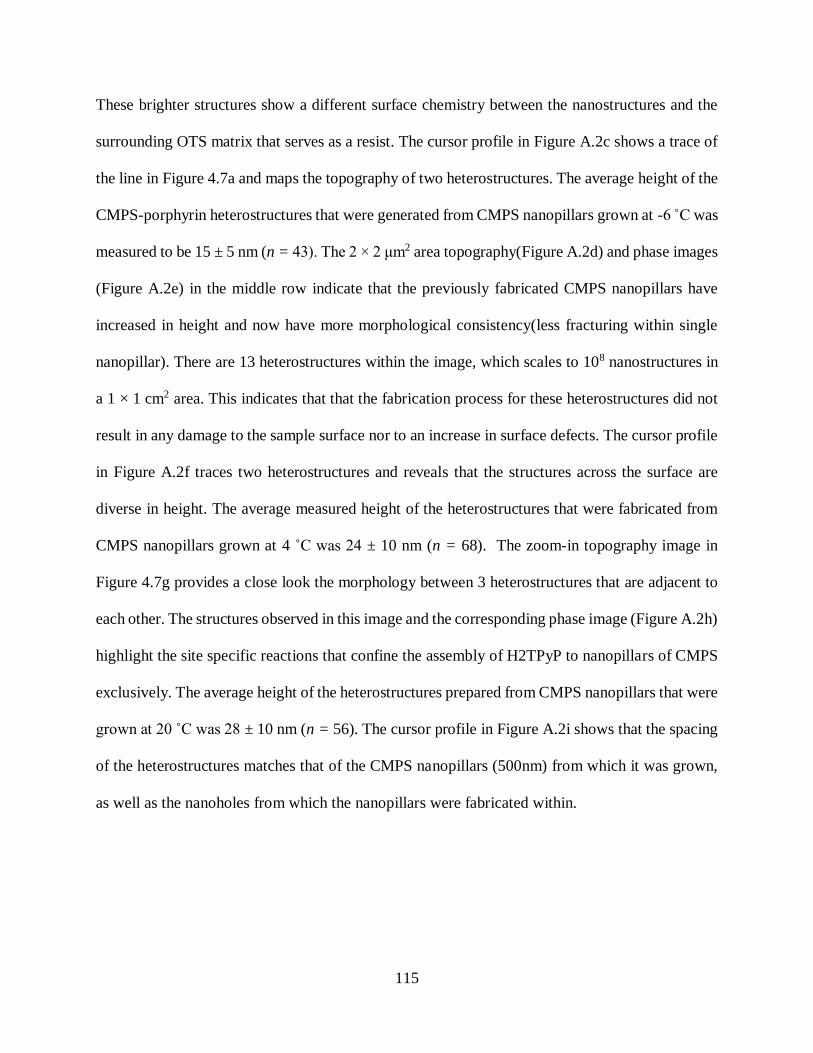
115
These brighter structures show a different surface chemistry between the nanostructures and the
surrounding OTS matrix that serves as a resist. The cursor profile in Figure A.2c shows a trace of
the line in Figure 4.7a and maps the topography of two heterostructures. The average height of the
CMPS-porphyrin heterostructures that were generated from CMPS nanopillars grown at -6 C was
measured to be 15 ± 5 nm (n = 43). The 2 × 2 μm2 area topography(Figure A.2d) and phase images
(Figure A.2e) in the middle row indicate that the previously fabricated CMPS nanopillars have
increased in height and now have more morphological consistency(less fracturing within single
nanopillar). There are 13 heterostructures within the image, which scales to 108 nanostructures in
a 1 × 1 cm2 area. This indicates that that the fabrication process for these heterostructures did not
result in any damage to the sample surface nor to an increase in surface defects. The cursor profile
in Figure A.2f traces two heterostructures and reveals that the structures across the surface are
diverse in height. The average measured height of the heterostructures that were fabricated from
CMPS nanopillars grown at 4 ˚C was 24 ± 10 nm (n = 68). The zoom-in topography image in
Figure 4.7g provides a close look the morphology between 3 heterostructures that are adjacent to
each other. The structures observed in this image and the corresponding phase image (Figure A.2h)
highlight the site specific reactions that confine the assembly of H2TPyP to nanopillars of CMPS
exclusively. The average height of the heterostructures prepared from CMPS nanopillars that were
grown at 20 ˚C was 28 ± 10 nm (n = 56). The cursor profile in Figure A.2i shows that the spacing
of the heterostructures matches that of the CMPS nanopillars (500nm) from which it was grown,
as well as the nanoholes from which the nanopillars were fabricated within.
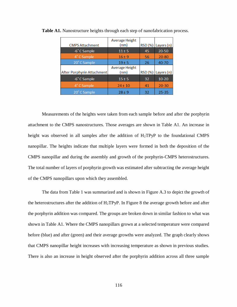
116
Table A1. Nanostructure heights through each step of nanofabrication process.
Measurements of the heights were taken from each sample before and after the porphyrin
attachment to the CMPS nanostructures. Those averages are shown in Table A1. An increase in
height was observed in all samples after the addition of H2TPyP to the foundational CMPS
nanopillar. The heights indicate that multiple layers were formed in both the deposition of the
CMPS nanopillar and during the assembly and growth of the porphyrin-CMPS heterostructures.
The total number of layers of porphyrin growth was estimated after subtracting the average height
of the CMPS nanopillars upon which they assembled.
The data from Table 1 was summarized and is shown in Figure A.3 to depict the growth of
the heterostructures after the addition of H2TPyP. In Figure 8 the average growth before and after
the porphyrin addition was compared. The groups are broken down in similar fashion to what was
shown in Table A1. Where the CMPS nanopillars grown at a selected temperature were compared
before (blue) and after (green) and their average growths were analyzed. The graph clearly shows
that CMPS nanopillar height increases with increasing temperature as shown in previous studies.
There is also an increase in height observed after the porphyrin addition across all three sample

117
groups. Each group experienced a statistically significant increase in height based upon a two-
tailed t-test analysis of means at a 95% confidence level.
Figure A.3. Heights of CMPS pillars (blue) and CMPS-porphyrin heterostructures (green).
118
VITA
Phillip Chambers Jr. was born in Dalton, Georgia to his parents, Phillip and Debbie
Chambers in January of 1990. He earned his High School Diploma from Loudoun Valley High
School in 2008 in Purcellville Virginia. He then attended James Madison University where he
obtained a bachelors of science in chemistry in 2012. While at James Madison, Phillip conducted
research under Dr. Daniel M. Downey where he led a new project to determine an elemental
fingerprint of a local invasive algal species using inductively coupled plasma mass-spectrometry.
His results were presented at National and local conferences around the country.
In 2012 Phillip decided to pursue a PhD in chemistry and chose to do so at Louisiana State
University. In 2013 He joined the Garno research Group at LSU and began learning about
nanoscale fabrication and surface characterization using techniques of scanning probe microscopy.
He has taught General chemistry labs, Analytical labs, as well as Instrumental Characterization
labs during his tenure at LSU. In research, he has contributed two first author manuscripts that
have been submitted for publication, two more first author publications that are in preparation as
well as three co-authored manuscripts that are in preparation. He has presented his research at
multiple national American Chemical Society conferences. He has mentored multiple
undergraduate students in the Garno Lab and helped to generate new research projects.