self-healing design methodologies for analog integrated ... · pdf fileself-healing design...
TRANSCRIPT
SELF-HEALING DESIGN
METHODOLOGIES FOR ANALOG
INTEGRATED CIRCUITS
Submitted in partial fulfillment of the requirements for
the degree of
Doctor of Philosophy
in
Electrical and Computer Engineering
Soner Yaldiz
B.S., Microelectronics, Sabanci University
M.S., Electrical and Computer Engineering, Koc University
Carnegie Mellon University
Pittsburgh, PA
January, 2012

Acknowledgments
I would like to express my gratitude to my advisor, Professor Larry Pileggi, whose vision,
expertise and optimism I admire. I would like to thank my dissertation committee members,
Professor Andrzej Strojwas (CMU), Professor Xin Li (CMU), Dr. Arun Natarajan (IBM)
and Dr. Vyacheslav (Slava) Rovner (PDF Solutions) for their guidance, help and feedback
during this work.
I would also like to express my gratitude to my love, Lale Muazzez Yaldiz, my parents,
Nadide and Nevzat Yaldiz, my brother Taner Yaldiz and his family, and all members of
Aricioglu family for their love and support.
I would like to thank Gokce Keskin for his close friendship, support, help to solve technical
issues and for motivating me whenever I get frustrated. I also would like to thank Pinar
Donmez, Volkan Ediz, Oznur Tastan, Tankut Dogrul, Umut Arslan, Emre Karagozler, Cagla
Cakir and Ekin Sumbul for their invaluable support and friendship.
I would like to thank Bodhisatwa Sadhu, Mark Ferriss, Jean-Olivier Plouchart, Scott
Reynolds, Jose Tierno and Daniel Friedman for their support, guidance and contributions
to this research during my internship at IBM. I also would like to thank Jian Wang, Jon
Proesel, Brian Taylor, Bin Wan, Yu-Tsun Chien, Vehbi Calayir, Fa Wang and numerous
other fellow students for their support, help and contributions.
This research has been supported by the Center for Circuit and System Solutions Fo-
cus Center, one of six research centers funded under the Focus Center Research Program,
a Semiconductor Research Corporation entity and sponsored by the Defense Advanced Re-
search Projects Agency Self-Healing Mixed-Signal Integrated Circuits program under Air
Force Research Laboratory contract FA8650-09-C-7924. The views expressed are those of
the author and do not reflect the official policy or position of the Department of Defense or
the United States Government.
ii

Abstract
Increasing process variability and shrinking voltage headroom in advanced silicon processes
have limited the efficacy of existing design and layout techniques, especially for analog circuits
that push the performance envelope. Process variations and high-performance specifications
has started to cause unpredictable and unacceptable product yield that requires new de-
sign methodologies with post-manufacturing tuning capability. Self-healing design style, in
which a tunable analog circuit is integrated together with performance sensors and a tuning
algorithm, can restore the performance loss due to process and environment variability. Fur-
thermore, self-healing can be utilized to optimize the circuits with multiple operating modes
where the performance is sensitive to the circuit state.
In this dissertation, we address what we consider to be the major challenges in designing
self-healing systems with digital tuning: integrated performance sensing; robust algorithm
design and verification before manufacturing. We present a general review of self-healing
design challenges, important design trade-offs and propose general guidelines. We propose
the use of indirect sensing for performance metrics that are either difficult or impractical to
measure using integrated circuits. We then present a catalog of techniques for self-healing
system verification including circuit simulation, behavioral modeling and simulation. We
also explore applicability of formal techniques towards verification of self-healing systems.
To demonstrate our work we focus specifically on self-healing challenges as they relate to
the design of phase locked loops (PLL) - a challenging design example that requires multiple
self-healing loops for higher performance. We apply indirect sensing method for phase noise
in voltage controlled oscillators and frequency response of PLL’s. We also present a hybrid
PLL model that enables reachability analysis and discuss the generalization of reachability
analysis to self-healing circuits.
iii

Contents
1 Introduction 1
1.1 Actuation . . . . . . . . . . . . . . . . . . . . . . . . . . . . . . . . . . . . . 3
1.2 Sensing . . . . . . . . . . . . . . . . . . . . . . . . . . . . . . . . . . . . . . . 4
1.3 Algorithm . . . . . . . . . . . . . . . . . . . . . . . . . . . . . . . . . . . . . 6
1.4 Verification . . . . . . . . . . . . . . . . . . . . . . . . . . . . . . . . . . . . 7
1.5 Contributions and Organization . . . . . . . . . . . . . . . . . . . . . . . . . 8
2 Background 10
2.1 Phase Locked Loop . . . . . . . . . . . . . . . . . . . . . . . . . . . . . . . . 10
2.2 Past Work . . . . . . . . . . . . . . . . . . . . . . . . . . . . . . . . . . . . . 14
2.3 Summary . . . . . . . . . . . . . . . . . . . . . . . . . . . . . . . . . . . . . 17
3 Indirect Performance Sensing 18
3.1 Indirect Sensor Design Methodology . . . . . . . . . . . . . . . . . . . . . . . 18
3.2 Indirect Phase Noise Sensing . . . . . . . . . . . . . . . . . . . . . . . . . . . 23
3.2.1 Differential Colpitts Oscillator . . . . . . . . . . . . . . . . . . . . . . 24
3.2.2 Linearized Transconductance Oscillator . . . . . . . . . . . . . . . . . 34
3.3 Indirect Frequency Response Sensing . . . . . . . . . . . . . . . . . . . . . . 41
3.3.1 Dual-Path Charge-Pump PLL . . . . . . . . . . . . . . . . . . . . . . 43
3.4 Summary . . . . . . . . . . . . . . . . . . . . . . . . . . . . . . . . . . . . . 49
iv

4 Verification of Self-Healing Systems 50
4.1 Overview of Analog Verification . . . . . . . . . . . . . . . . . . . . . . . . . 51
4.2 Actuation . . . . . . . . . . . . . . . . . . . . . . . . . . . . . . . . . . . . . 53
4.3 Sensor . . . . . . . . . . . . . . . . . . . . . . . . . . . . . . . . . . . . . . . 55
4.4 Algorithm . . . . . . . . . . . . . . . . . . . . . . . . . . . . . . . . . . . . . 60
4.5 Summary . . . . . . . . . . . . . . . . . . . . . . . . . . . . . . . . . . . . . 67
5 Towards Formal Verification of Self-Healing Systems 69
5.1 Overview of Formal Analog Verification . . . . . . . . . . . . . . . . . . . . . 69
5.2 Reachability Analysis for PLL . . . . . . . . . . . . . . . . . . . . . . . . . . 72
5.3 Discussion . . . . . . . . . . . . . . . . . . . . . . . . . . . . . . . . . . . . . 78
6 Conclusion 79
Appendices 88
.1 Behavioral Model of Phase Frequency Detector and Charge Pump in Verilog-
AMS . . . . . . . . . . . . . . . . . . . . . . . . . . . . . . . . . . . . . . . . 89
.2 Behavioral Model of Voltage Controlled Oscillator and Frequency Divider in
Verilog-AMS . . . . . . . . . . . . . . . . . . . . . . . . . . . . . . . . . . . . 92
v

List of Tables
3.1 Indirect phase noise sensor accuracy . . . . . . . . . . . . . . . . . . . . . . . 38
3.2 VCO Tank Parameters . . . . . . . . . . . . . . . . . . . . . . . . . . . . . . 44
3.3 PLL parameters and metrics . . . . . . . . . . . . . . . . . . . . . . . . . . . 46
vi
List of Figures
1.1 Self-healing system with digital tuning. . . . . . . . . . . . . . . . . . . . . . 3
1.2 Insufficient tuning range and resolution. . . . . . . . . . . . . . . . . . . . . 4
1.3 Iterative heuristic search for non-convex and convex actuation. . . . . . . . . 7
2.1 Charge-pump phase locked loop. . . . . . . . . . . . . . . . . . . . . . . . . . 11
2.2 Dual-path charge-pump phase locked loop. . . . . . . . . . . . . . . . . . . . 12
2.3 Phase locking in charge-pump phase locked loop. . . . . . . . . . . . . . . . 13
2.4 Power spectrum of VCO signal with and without phase noise. . . . . . . . . 13
2.5 LC tank with digitally switched capacitor array. . . . . . . . . . . . . . . . . 15
2.6 Digital automatic amplitude control loop. . . . . . . . . . . . . . . . . . . . . 16
2.7 On-chip phase noise sensor. . . . . . . . . . . . . . . . . . . . . . . . . . . . 16
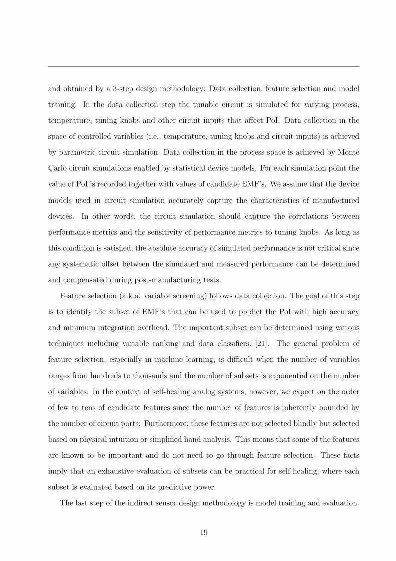
2.8 On-chip period jitter sensor. . . . . . . . . . . . . . . . . . . . . . . . . . . . 17
3.1 Self-healing using indirect performance sensor. . . . . . . . . . . . . . . . . . 22
3.2 Differential Colpitts voltage controlled oscillator. . . . . . . . . . . . . . . . . 25
3.3 Tuning of differential Colpitts VCO under nominal conditions. . . . . . . . . 26
3.4 Variation in phase noise of differential Colpitts VCO due to coarse frequency
bands. . . . . . . . . . . . . . . . . . . . . . . . . . . . . . . . . . . . . . . . 27
3.5 Variation in phase noise of differential Colpitts VCO due to temperature. . . 27
3.6 Variation in phase noise of differential Colpitts VCO due to process. . . . . . 28
3.7 RMS error in estimated phase noise versus polynomial order. . . . . . . . . . 29
vii

3.8 RMS error in estimated phase noise versus number of non-zero coefficients in
quadratic model. . . . . . . . . . . . . . . . . . . . . . . . . . . . . . . . . . 29
3.9 Simulated phase noise versus phase noise estimated by indirect sensor. . . . . 30
3.10 Self-healing algorithm for VCO phase noise. . . . . . . . . . . . . . . . . . . 31
3.11 Simulated parametric yield of phase noise achieved by ideal, non-healing and
self-healing design for varying target. . . . . . . . . . . . . . . . . . . . . . . 32
3.12 Normalized simulated average power dissipation of ideal, non-healing and self-
healing design. . . . . . . . . . . . . . . . . . . . . . . . . . . . . . . . . . . 33
3.13 Linearized transconductance VCO. . . . . . . . . . . . . . . . . . . . . . . . 35
3.14 Tuning of linearized transconductance VCO under nominal conditions. . . . 36
3.15 Variation in phase noise of linearized transconductance VCO due to coarse
frequency bands. . . . . . . . . . . . . . . . . . . . . . . . . . . . . . . . . . 37
3.16 Variation in phase noise of linearized transconductance VCO due to process. 37
3.17 RMS error in estimated phase noise versus polynomial order. . . . . . . . . . 39
3.18 RMS error in estimated phase noise versus number of non-zero coefficients in
quadratic model. . . . . . . . . . . . . . . . . . . . . . . . . . . . . . . . . . 39
3.19 Measured parametric yield of phase noise achieved by ideal, non-healing and
self-healing design for varying target. . . . . . . . . . . . . . . . . . . . . . . 40
3.20 Normalized measured average power dissipation of ideal, non-healing and self-
healing design. . . . . . . . . . . . . . . . . . . . . . . . . . . . . . . . . . . 40
3.21 Phase error injection by temporary change in division ratio. . . . . . . . . . 42
3.22 Crossover and overshoot measurement in prior work. . . . . . . . . . . . . . 42
3.23 Single and proposed repetitive phase error injection. . . . . . . . . . . . . . . 43
3.24 VCO frequency versus integral path voltage. . . . . . . . . . . . . . . . . . . 45
3.25 VCO frequency gain versus input voltage. . . . . . . . . . . . . . . . . . . . 45
3.26 Gain peaking versus bandwidth in the simulated data. . . . . . . . . . . . . 46
3.27 Bandwidth versus first crossover. . . . . . . . . . . . . . . . . . . . . . . . . 47
viii
3.28 Gain peaking versus first crossover. . . . . . . . . . . . . . . . . . . . . . . . 47
3.29 Accuracy of indirect bandwidth sensor for varying number of repetitions. . . 48
3.30 Accuracy of indirect gain peaking sensor for varying number of repetitions. . 48
4.1 Divide-by-2 prescaler with tunable resistive loads and bias voltage. . . . . . . 54
4.2 Charge pump up and down currents as a function of output voltage. . . . . . 56
4.3 Comparison of hyperbolic tangent approximation of the varactor with circuit
simulation. . . . . . . . . . . . . . . . . . . . . . . . . . . . . . . . . . . . . . 57
4.4 Frequency tuning and gain curves for at band 13. . . . . . . . . . . . . . . . 58
4.5 Transient simulation of different PLL models. . . . . . . . . . . . . . . . . . 60
4.6 Transient simulation of the nonlinear PLL model at two different frequencies. 61
4.7 Crossover measurement in the presence of static offset. . . . . . . . . . . . . 61
4.8 Self-healing system with actuation and sensing delay. . . . . . . . . . . . . . 62
4.9 Frequency band selection algorithm. . . . . . . . . . . . . . . . . . . . . . . . 63
4.10 Transient simulation of frequency selection algorithm for NWAIT = 16. . . . . 64
4.11 Transient simulation of frequency selection algorithm for NWAIT = 32. . . . . 64
4.12 Transient simulation of frequency selection algorithm for NWAIT = 64. . . . . 65
4.13 Transient simulation of frequency selection algorithm for NWAIT = 128. . . . 65
4.14 Analog system with multiple self-healing loops. . . . . . . . . . . . . . . . . 66
4.15 Unstable system due to interdependent self-healing loops. . . . . . . . . . . . 67
4.16 PLL with multiple self-healing loops. . . . . . . . . . . . . . . . . . . . . . . 68
5.1 Fourth order dual-path charge-pump phase locked loop. . . . . . . . . . . . . 73
5.2 Hybrid automaton for phase frequency detector. . . . . . . . . . . . . . . . . 76
5.3 Reachable sets of the first 200 cycles. . . . . . . . . . . . . . . . . . . . . . . 78
ix
Chapter 1
Introduction
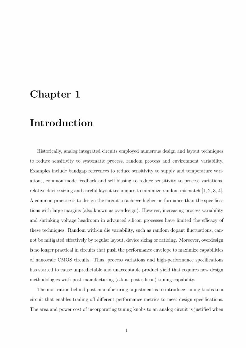
Historically, analog integrated circuits employed numerous design and layout techniques
to reduce sensitivity to systematic process, random process and environment variability.
Examples include bandgap references to reduce sensitivity to supply and temperature vari-
ations, common-mode feedback and self-biasing to reduce sensitivity to process variations,
relative device sizing and careful layout techniques to minimize random mismatch [1, 2, 3, 4].
A common practice is to design the circuit to achieve higher performance than the specifica-
tions with large margins (also known as overdesign). However, increasing process variability
and shrinking voltage headroom in advanced silicon processes have limited the efficacy of
these techniques. Random with-in die variability, such as random dopant fluctuations, can-
not be mitigated effectively by regular layout, device sizing or ratioing. Moreover, overdesign
is no longer practical in circuits that push the performance envelope to maximize capabilities
of nanoscale CMOS circuits. Thus, process variations and high-performance specifications
has started to cause unpredictable and unacceptable product yield that requires new design
methodologies with post-manufacturing (a.k.a. post-silicon) tuning capability.
The motivation behind post-manufacturing adjustment is to introduce tuning knobs to a
circuit that enables trading off different performance metrics to meet design specifications.
The area and power cost of incorporating tuning knobs to an analog circuit is justified when
1

this overhead is smaller than the overhead required by the more traditional means such as
device sizing, or when traditional means are not effective to mitigate systematic and random
variations in performance. Post-manufacturing tuning has already been demonstrated for
various analog and radio frequency (RF) circuits in the literature [4, 5, 6].
One further step toward performance maximization in nanoscale CMOS circuits is the
self-healing design style in which the tunable circuit is integrated together with perfor-
mance sensors and a tuning algorithm. Self-healing design can significantly reduce the post-
manufacturing test and calibration cost by utilizing integrated sensing and control circuitry
and restore performance loss due to environment variability. Furthermore, self-healing can
be utilized to optimize the circuits with multiple operating modes where the performance is
sensitive to the circuit state.
In this thesis we use the term self-healing design (SHD) to refer to a system that can au-
tonomously calibrate itself to achieve an objective using digital tuning as shown in Figure 1.1.
Traditionally, self-healing techniques have been based on analog feedback that suffers from
variations and creates stability concerns [2, 3]. To the contrary, a digital control loop can
be guaranteed to be stable by construction. A digital control loop can be disabled after cal-
ibration unlike continuous feedback loops to avoid perturbing or modulating the circuit. In
addition, digital circuits are easier to design and more robust than analog circuits. Therefore,
we focus only on self-healing via digital tuning that refers to selection of a subset of devices
and/or discrete biasing levels. Digital tuning is widely applicable and enables actuation in
newer process technologies with decreasing voltage headroom.
The objective of self-healing can be to meet performance specifications in the presence
of variability to maximize product yield, to reduce power dissipation (which is particularly
important for mobile systems), to enable new applications in nanoscale CMOS, and/or to
reduce post-manufacturing test cost. A complex SHD may incorporate multiple self-healing
loops. The justification of SHD depends primarily on the integration overhead that includes
area, power and calibration time. The increased design complexity and associated verification
2
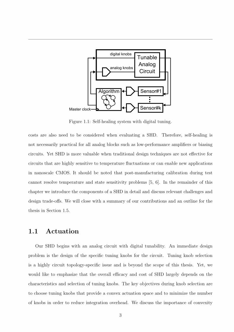
Figure 1.1: Self-healing system with digital tuning.
costs are also need to be considered when evaluating a SHD. Therefore, self-healing is
not necessarily practical for all analog blocks such as low-performance amplifiers or biasing
circuits. Yet SHD is more valuable when traditional design techniques are not effective for
circuits that are highly sensitive to temperature fluctuations or can enable new applications
in nanoscale CMOS. It should be noted that post-manufacturing calibration during test
cannot resolve temperature and state sensitivity problems [5, 6]. In the remainder of this
chapter we introduce the components of a SHD in detail and discuss relevant challenges and
design trade-offs. We will close with a summary of our contributions and an outline for the
thesis in Section 1.5.
1.1 Actuation
Our SHD begins with an analog circuit with digital tunability. An immediate design
problem is the design of the specific tuning knobs for the circuit. Tuning knob selection
is a highly circuit topology-specific issue and is beyond the scope of this thesis. Yet, we
would like to emphasize that the overall efficacy and cost of SHD largely depends on the
characteristics and selection of tuning knobs. The key objectives during knob selection are
to choose tuning knobs that provide a convex actuation space and to minimize the number
of knobs in order to reduce integration overhead. We discuss the importance of convexity
3
further in the following sections and chapters.
The secondary design problems are the range and resolution of tuning. The tuning range
should be sufficient to be able to meet self-healing objectives under extreme variability. The
tuning resolution depends on the resolution of performance sensors. Low tuning resolution
is preferable to reduce integration overhead. However, the resolution should be sufficient
for the self-healing loop to converge to a feasible solution. The tuning range and resolution
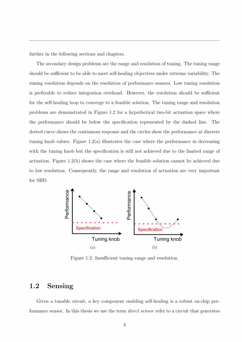
problems are demonstrated in Figure 1.2 for a hypothetical two-bit actuation space where
the performance should be below the specification represented by the dashed line. The
dotted curve shows the continuous response and the circles show the performance at discrete
tuning knob values. Figure 1.2(a) illustrates the case where the performance in decreasing
with the tuning knob but the specification is still not achieved due to the limited range of
actuation. Figure 1.2(b) shows the case where the feasible solution cannot be achieved due
to low resolution. Consequently, the range and resolution of actuation are very important
for SHD.
Tuning knob
Perf
orm
ance
Specification
(a)
Tuning knob
Perf
orm
ance
Specification
(b)
Figure 1.2: Insufficient tuning range and resolution.
1.2 Sensing
Given a tunable circuit, a key component enabling self-healing is a robust on-chip per-
formance sensor. In this thesis we use the term direct sensor refer to a circuit that generates
4

an output signal explicitly quantifying the performance of interest (PoI). Examples of direct
sensors include analog to digital converters, time to digital converters, frequency counters,
amplitude detectors and thermal sensors.
Our experience with actual designs has shown that robust direct sensors may not be
available or practical for some performance metrics such as phase noise or bandwidth. For
such performance metrics, the integration overhead, the vulnerability to variability (where
the sensor itself may require self-healing) or physical limitations (where the sensor cannot
provide sufficient resolution) can prohibit design of direct sensors. To overcome these chal-
lenges we propose the use of indirect performance sensors (IPS) that predict the PoI as a
function of other easy-to-measure performance metrics, already-known circuit inputs and
tuning knobs. Indirect performance sensing can be particularly used to estimate the PoI in
the presence of global process shifts, temperature fluctuations or device nonlinearities. The
actuation and self-healing for local mismatch between devices has been addressed in [7].
In this thesis we use the term easy-to-measure features (EMF) to refer to all independent
variables that can be used to predict PoI. IPS exploits the correlations between/the sensitiv-
ity of PoI and/to EMF. IPS relies on the fact that analog behaviors are complex, nonlinear
functions of the same set of underlying design, process and environment variables. This
implies that we can find EMF’s that correlate well with specific PoI. If such EMF’s cannot
be identified, then a divide-and-conquer style approach can be followed to attack different
sources of variability. In this case, performance degradation due to process variability can be
corrected by external sensing and calibration during post-manufacturing tests, leaving only
temperature and input sensitivity to be self-healed at runtime. The design methodology for
IPS is explained in further detail and demonstrated using circuit examples in Chapter 3.
5

1.3 Algorithm
Performance optimization of analog circuits with digital tunability is a combinatorial
optimization problem (a.k.a. integer programming problem) due to the discrete actuation
space. Specifications on performance metrics correspond to constraints and the objective
depends on the application. Various techniques (e.g., enumeration, relaxation) have been
presented in the literature to solve combinatorial optimization problems that are shown to be
NP-hard. Yet heuristic approaches are usually preferred to find a solution quickly. The lack
or limited availability of exact closed-form analytical formulations of analog performance
metrics also make heuristic approaches more preferable for self-healing.
The design of a self-healing algorithm primarily depends on the time interval available
for calibration and the characteristics of the actuation space with the goal of minimum
integration overhead. The simplest self-healing algorithm is the exhaustive search in the
actuation space that can be implemented by digital counters and comparators. This brute-
force approach might be sufficient for systems that do not have timing constraints on the
self-healing loop convergence or might be the only option for systems where the objective is
minimizing mismatch between identical elements. Despite its simplicity, exhaustive search
may be impractical for systems that require frequent calibration and have timing constraints
on the settling time of calibration. In such cases, minimizing the number of tuning knobs
and the number of configurations for each tuning knob become more important.
When exhaustive search is impractical, heuristic search algorithms that iteratively adjust
tuning knobs can be adopted and implemented using finite state machines. Examples of
heuristic search algorithms include bisection, line search or gradient descent. While they
offer simplicity, heuristic algorithms can become stuck at local optimums if the PoI is not a
convex function of tuning knobs, as demonstrated by toy examples in Figure 1.3. Figure 1.3
shows two hypothetical three-bit actuation mechanisms where the performance should be
below the specification represented by the dashed line. Figure 1.3(a) illustrates a non-convex
actuation space where an iterative search beginning at the initial point terminates at an
6
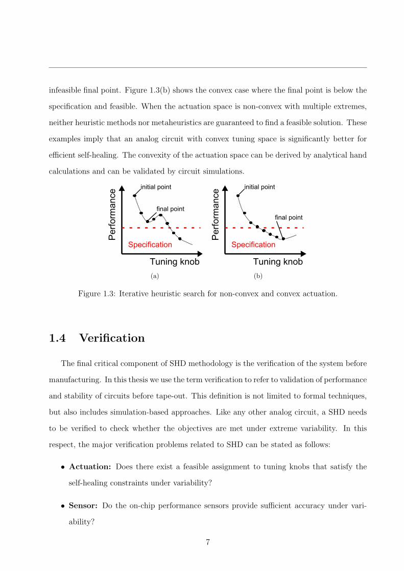
infeasible final point. Figure 1.3(b) shows the convex case where the final point is below the
specification and feasible. When the actuation space is non-convex with multiple extremes,
neither heuristic methods nor metaheuristics are guaranteed to find a feasible solution. These
examples imply that an analog circuit with convex tuning space is significantly better for
efficient self-healing. The convexity of the actuation space can be derived by analytical hand
calculations and can be validated by circuit simulations.
Tuning knob
Pe
rfo
rma
nce
Specification
initial point
final point
(a)
Tuning knob
Pe
rfo
rma
nce
Specification
initial point
final point
(b)
Figure 1.3: Iterative heuristic search for non-convex and convex actuation.
1.4 Verification
The final critical component of SHD methodology is the verification of the system before
manufacturing. In this thesis we use the term verification to refer to validation of performance
and stability of circuits before tape-out. This definition is not limited to formal techniques,
but also includes simulation-based approaches. Like any other analog circuit, a SHD needs
to be verified to check whether the objectives are met under extreme variability. In this
respect, the major verification problems related to SHD can be stated as follows:
• Actuation: Does there exist a feasible assignment to tuning knobs that satisfy the
self-healing constraints under variability?
• Sensor: Do the on-chip performance sensors provide sufficient accuracy under vari-
ability?
7

• Stability: Is the SHD that consists of a single or multiple self-healing loops stable
under variability?
In Chapter 4, we discuss the applicability and limits of formal techniques to these problems
and present alternative verification strategies based on behavioral modeling and simulation.
1.5 Contributions and Organization
In this thesis we address what we consider to be the major challenges in designing self-
healing systems with digital tuning: 1) integrated performance sensing; 2) robust algorithm
design and 3) the verification of self-tuning circuits before manufacturing. To demonstrate
our work we focus specifically on these challenges as they relate to the design of phase locked
loops (PLL) - an important component of both communication and computing systems. A
challenging design that requires self-healing for higher performance, such as a high frequency
PLL, is necessary to solidify our contributions and validate the efficacy of our work. The
key contributions of this thesis can be summarized as follows:
1. We present a general review of self-healing design challenges, identify important design
trade-offs and propose practical solutions for PLL’s.
2. We propose indirect sensing method for performance metrics that are either difficult
or impractical to measure using integrated sensors.
3. We present a catalog of techniques for self-healing system verification ranging from
circuit simulation to formal verification and demonstrate using realistic examples.
The remaining chapters are organized as follows. In Chapter 2 we provide the background
and existing self-healing solutions on circuits and systems discussed in this thesis. In Chap-
ter 3 we describe and demonstrate indirect performance sensing for phase noise in voltage
controlled oscillators (VCO) and for frequency response of PLL’s. In Chapter 4 we present
8

verification strategies for self-healing systems and demonstrate using relevant circuit exam-
ples. We explore formal techniques towards verification of self-healing systems in Chapter 5.
We conclude the thesis with possible future directions in Chapter 6.
9
Chapter 2
Background
To demonstrate the techniques presented in this thesis we will focus specifically on chal-
lenges in the design of self-healing phase locked loops (PLL). A complex design platform and
example that requires self-healing for higher performance, such as the PLL, is necessary for
evaluating the efficacy of our work. In this chapter we will first provide a brief introduction to
phase locked loops and explain the major performance issues demanding post-manufacturing
tunability. In Section 2.2 we will present an overview of previous art in post-manufacturing
tunability of PLL performance metrics.
2.1 Phase Locked Loop
A phase locked loop (PLL) is a dynamic feedback circuit that is used to synthesize a low-
noise, high-frequency periodic signal on a chip using an external, constant and low-frequency
reference signal. This is achieved by applying frequency division to the high-frequency signal
and then locking the phase and frequency of the divided feedback signal to the reference
signal. The high frequency signal is generated by a voltage controlled oscillator (VCO)
where its input voltage controls the frequency of oscillation. By changing the frequency
division ratio (NDIV ), the frequency of the VCO signal (fV CO) can be controlled precisely
10
as follows:
fV CO = NDIV × fREF (2.1)
where fREF is the frequency of the reference signal. In computing systems, the output signal
is used as a clock signal for synchronous digital circuits, while it is used as a local oscillator
signal for frequency conversion in communication circuits.
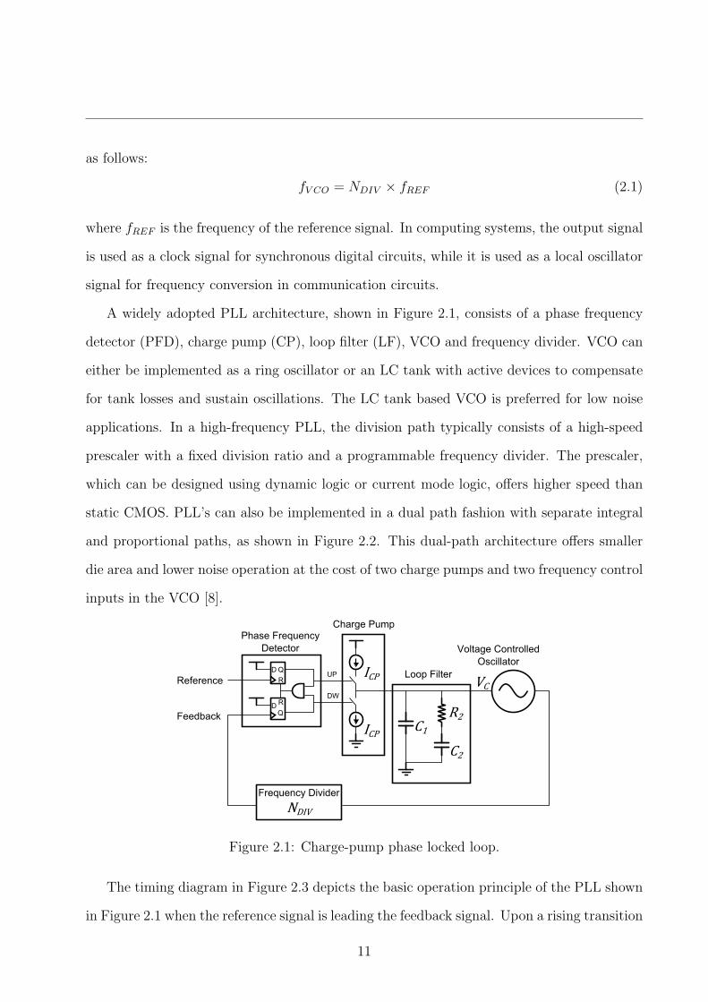
A widely adopted PLL architecture, shown in Figure 2.1, consists of a phase frequency
detector (PFD), charge pump (CP), loop filter (LF), VCO and frequency divider. VCO can
either be implemented as a ring oscillator or an LC tank with active devices to compensate
for tank losses and sustain oscillations. The LC tank based VCO is preferred for low noise
applications. In a high-frequency PLL, the division path typically consists of a high-speed
prescaler with a fixed division ratio and a programmable frequency divider. The prescaler,
which can be designed using dynamic logic or current mode logic, offers higher speed than
static CMOS. PLL’s can also be implemented in a dual path fashion with separate integral
and proportional paths, as shown in Figure 2.2. This dual-path architecture offers smaller
die area and lower noise operation at the cost of two charge pumps and two frequency control
inputs in the VCO [8].
Figure 2.1: Charge-pump phase locked loop.
The timing diagram in Figure 2.3 depicts the basic operation principle of the PLL shown
in Figure 2.1 when the reference signal is leading the feedback signal. Upon a rising transition
11
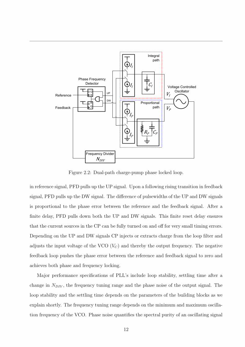
Figure 2.2: Dual-path charge-pump phase locked loop.
in reference signal, PFD pulls up the UP signal. Upon a following rising transition in feedback
signal, PFD pulls up the DW signal. The difference of pulsewidths of the UP and DW signals
is proportional to the phase error between the reference and the feedback signal. After a
finite delay, PFD pulls down both the UP and DW signals. This finite reset delay ensures
that the current sources in the CP can be fully turned on and off for very small timing errors.
Depending on the UP and DW signals CP injects or extracts charge from the loop filter and
adjusts the input voltage of the VCO (VC) and thereby the output frequency. The negative
feedback loop pushes the phase error between the reference and feedback signal to zero and
achieves both phase and frequency locking.
Major performance specifications of PLL’s include loop stability, settling time after a
change in NDIV , the frequency tuning range and the phase noise of the output signal. The
loop stability and the settling time depends on the parameters of the building blocks as we
explain shortly. The frequency tuning range depends on the minimum and maximum oscilla-
tion frequency of the VCO. Phase noise quantifies the spectral purity of an oscillating signal
12
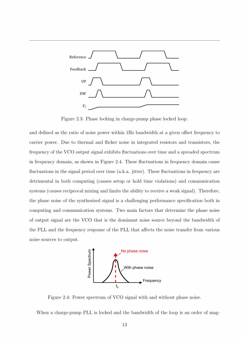
Figure 2.3: Phase locking in charge-pump phase locked loop.
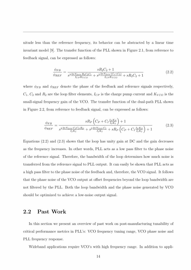
and defined as the ratio of noise power within 1Hz bandwidth at a given offset frequency to
carrier power. Due to thermal and flicker noise in integrated resistors and transistors, the
frequency of the VCO output signal exhibits fluctuations over time and a spreaded spectrum
in frequency domain, as shown in Figure 2.4. These fluctuations in frequency domain cause
fluctuations in the signal period over time (a.k.a. jitter). These fluctuations in frequency are
detrimental in both computing (causes setup or hold time violations) and communication
systems (causes reciprocal mixing and limits the ability to receive a weak signal). Therefore,
the phase noise of the synthesized signal is a challenging performance specification both in
computing and communication systems. Two main factors that determine the phase noise
of output signal are the VCO that is the dominant noise source beyond the bandwidth of
the PLL and the frequency response of the PLL that affects the noise transfer from various
noise sources to output.
Figure 2.4: Power spectrum of VCO signal with and without phase noise.
When a charge-pump PLL is locked and the bandwidth of the loop is an order of mag-
13
nitude less than the reference frequency, its behavior can be abstracted by a linear time
invariant model [9]. The transfer function of the PLL shown in Figure 2.1, from reference to
feedback signal, can be expressed as follows:
φFB
φREF
=sR2C2 + 1
s3 2πNDIV R2C2C1
ICPKV CO
+ s2 2πNDIV (C1+C2)ICPKV CO
+ sR2C2 + 1(2.2)
where φFB and φREF denote the phase of the feedback and reference signals respectively,
C1, C2 and R2 are the loop filter elements, ICP is the charge pump current and KV CO is the
small-signal frequency gain of the VCO. The transfer function of the dual-path PLL shown
in Figure 2.2, from reference to feedback signal, can be expressed as follows:
φFB
φREF
=sRP
(
CP + CIIPKP
IIKI
)
+ 1
s3 2πNDIV CICPRP
IIKI
+ s2 2πNDIV CI
IIKI
+ sRP
(
CP + CIIPKP
IIKI
)
+ 1(2.3)
Equations (2.2) and (2.3) shows that the loop has unity gain at DC and the gain decreases
as the frequency increases. In other words, PLL acts as a low pass filter to the phase noise
of the reference signal. Therefore, the bandwidth of the loop determines how much noise is
transferred from the reference signal to PLL output. It can easily be shown that PLL acts as
a high pass filter to the phase noise of the feedback and, therefore, the VCO signal. It follows
that the phase noise of the VCO output at offset frequencies beyond the loop bandwidth are
not filtered by the PLL. Both the loop bandwidth and the phase noise generated by VCO
should be optimized to achieve a low-noise output signal.
2.2 Past Work
In this section we present an overview of past work on post-manufacturing tunability of
critical performance metrics in PLL’s: VCO frequency tuning range, VCO phase noise and
PLL frequency response.
Wideband applications require VCO’s with high frequency range. In addition to appli-
14
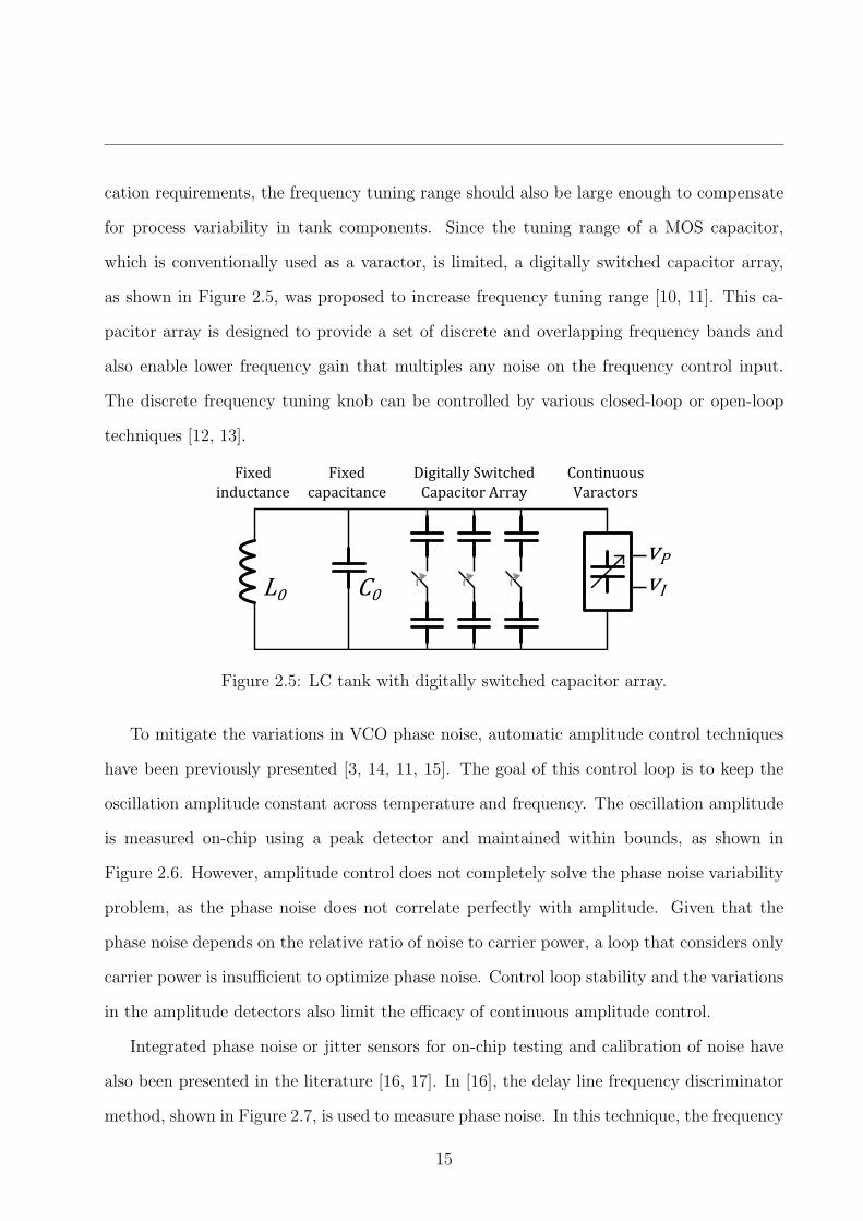
cation requirements, the frequency tuning range should also be large enough to compensate
for process variability in tank components. Since the tuning range of a MOS capacitor,
which is conventionally used as a varactor, is limited, a digitally switched capacitor array,
as shown in Figure 2.5, was proposed to increase frequency tuning range [10, 11]. This ca-
pacitor array is designed to provide a set of discrete and overlapping frequency bands and
also enable lower frequency gain that multiples any noise on the frequency control input.
The discrete frequency tuning knob can be controlled by various closed-loop or open-loop
techniques [12, 13].
Figure 2.5: LC tank with digitally switched capacitor array.
To mitigate the variations in VCO phase noise, automatic amplitude control techniques
have been previously presented [3, 14, 11, 15]. The goal of this control loop is to keep the
oscillation amplitude constant across temperature and frequency. The oscillation amplitude
is measured on-chip using a peak detector and maintained within bounds, as shown in
Figure 2.6. However, amplitude control does not completely solve the phase noise variability
problem, as the phase noise does not correlate perfectly with amplitude. Given that the
phase noise depends on the relative ratio of noise to carrier power, a loop that considers only
carrier power is insufficient to optimize phase noise. Control loop stability and the variations
in the amplitude detectors also limit the efficacy of continuous amplitude control.
Integrated phase noise or jitter sensors for on-chip testing and calibration of noise have
also been presented in the literature [16, 17]. In [16], the delay line frequency discriminator
method, shown in Figure 2.7, is used to measure phase noise. In this technique, the frequency
15
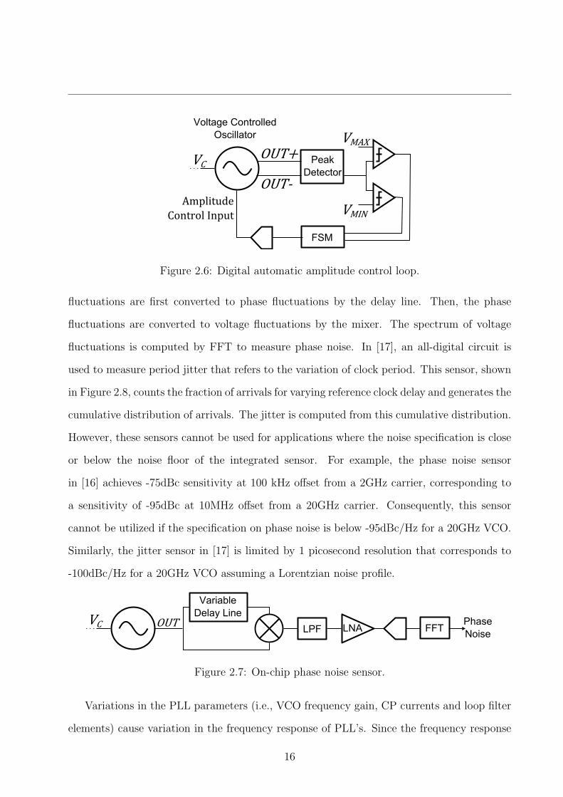
Figure 2.6: Digital automatic amplitude control loop.
fluctuations are first converted to phase fluctuations by the delay line. Then, the phase
fluctuations are converted to voltage fluctuations by the mixer. The spectrum of voltage
fluctuations is computed by FFT to measure phase noise. In [17], an all-digital circuit is
used to measure period jitter that refers to the variation of clock period. This sensor, shown
in Figure 2.8, counts the fraction of arrivals for varying reference clock delay and generates the
cumulative distribution of arrivals. The jitter is computed from this cumulative distribution.
However, these sensors cannot be used for applications where the noise specification is close
or below the noise floor of the integrated sensor. For example, the phase noise sensor
in [16] achieves -75dBc sensitivity at 100 kHz offset from a 2GHz carrier, corresponding to
a sensitivity of -95dBc at 10MHz offset from a 20GHz carrier. Consequently, this sensor
cannot be utilized if the specification on phase noise is below -95dBc/Hz for a 20GHz VCO.
Similarly, the jitter sensor in [17] is limited by 1 picosecond resolution that corresponds to
-100dBc/Hz for a 20GHz VCO assuming a Lorentzian noise profile.
Figure 2.7: On-chip phase noise sensor.
Variations in the PLL parameters (i.e., VCO frequency gain, CP currents and loop filter
elements) cause variation in the frequency response of PLL’s. Since the frequency response
16
Figure 2.8: On-chip period jitter sensor.
affects the noise of the synthesized signal and the PLL settling time, self-biasing techniques
have been proposed to mitigate variations in PLL bandwidth [2, 18, 19]. The key idea of
self-biasing is to adjust the CP currents proportional to the VCO frequency gain to keep
PLL bandwidth constant. However, self-biasing is mostly applicable to PLL’s with ring
oscillators. In [19], Wu et. al apply self-biasing to a PLL with LC tank VCO where CP
current is proportional to oscillation frequency and an averaging varactor is used to linearize
frequency gain. Apart from self-biasing techniques, Fischette et. al proposed an all-digital
sensor for on-chip estimation of PLL bandwidth and gain peaking in [20]. This sensor relies
on the relationship between the time-domain and frequency-domain response of linear time
invariant systems. However, this technique suffers from low accuracy for highly nonlinear
PLL’s with reduced supply voltage as will be explained in further detail in Section 3.3.
2.3 Summary
In this chapter we presented a brief background on charge-pump phase locked loops.
We explained how the circuit operates and major performance issues demanding post-
manufacturing tunability. Secondly, we provided an overview of previous work on post-
manufacturing tunability of PLL performance metrics, namely VCO frequency tuning range,
VCO phase noise and PLL frequency response. In the next chapter we will introduce and
demonstrate indirect performance sensing for VCO phase noise and PLL frequency response.
17

Chapter 3
Indirect Performance Sensing
A major challenge for self-healing systems is the efficient design of on-chip sensors that
quantify the performance of interest. This is particularly difficult for performance metrics
such as phase noise or bandwidth that are not easily measured on-chip either due to high
integration overhead or physical limitations. In this chapter we propose indirect performance
sensing that exploits correlations between the performance metrics of interest and those
that can be measured using easy-to-integrate sensors. In Section 3.1 we present a design
methodology for indirect performance sensors. In Section 3.2 we demonstrate and validate
this methodology for sensing phase noise of two different VCO architectures with simulated
and measured results. In Section 3.3 we apply this methodology for bandwidth and gain
peaking estimation in PLL’s. We summarize the chapter in Section 3.4.
3.1 Indirect Sensor Design Methodology
We use the term indirect performance sensor to refer to a static and deterministic math-
ematical model in the form of an explicit equation. This mathematical model predicts the
performance of interest (PoI) as a linear or nonlinear function of EMF’s as follows:
PoI = f (EMF1, ..,EMFk) (3.1)
18
and obtained by a 3-step design methodology: Data collection, feature selection and model
training. In the data collection step the tunable circuit is simulated for varying process,
temperature, tuning knobs and other circuit inputs that affect PoI. Data collection in the
space of controlled variables (i.e., temperature, tuning knobs and circuit inputs) is achieved
by parametric circuit simulation. Data collection in the process space is achieved by Monte
Carlo circuit simulations enabled by statistical device models. For each simulation point the
value of PoI is recorded together with values of candidate EMF’s. We assume that the device
models used in circuit simulation accurately capture the characteristics of manufactured
devices. In other words, the circuit simulation should capture the correlations between
performance metrics and the sensitivity of performance metrics to tuning knobs. As long as
this condition is satisfied, the absolute accuracy of simulated performance is not critical since
any systematic offset between the simulated and measured performance can be determined
and compensated during post-manufacturing tests.
Feature selection (a.k.a. variable screening) follows data collection. The goal of this step
is to identify the subset of EMF’s that can be used to predict the PoI with high accuracy
and minimum integration overhead. The important subset can be determined using various
techniques including variable ranking and data classifiers. [21]. The general problem of
feature selection, especially in machine learning, is difficult when the number of variables
ranges from hundreds to thousands and the number of subsets is exponential on the number
of variables. In the context of self-healing analog systems, however, we expect on the order
of few to tens of candidate features since the number of features is inherently bounded by
the number of circuit ports. Furthermore, these features are not selected blindly but selected
based on physical intuition or simplified hand analysis. This means that some of the features
are known to be important and do not need to go through feature selection. These facts
imply that an exhaustive evaluation of subsets can be practical for self-healing, where each
subset is evaluated based on its predictive power.
The last step of the indirect sensor design methodology is model training and evaluation.
19

Similar to the feature selection, circuit-specific information can again be used to determine
the model template. When such information is not available, nonlinear polynomial regression
can be used to express PoI as a function of selected EMF’s. The polynomial order depends
on the nonlinearity of the response surface and can be determined by cross-validation. In
cross-validation technique the data set is randomly partitioned into training and validation
subsets. The training set is used for regression while the validation set that is not used during
regression is used to evaluate predictive power. The polynomial coefficients are calculated
by solving the following unconstrained convex optimization problem that minimizes the root
mean squared (rms) error between the predicted and actual performance over the samples
minimize
‖Mα− b‖22
(3.2)
where M is an n-by-c matrix where each row contains the values of polynomial terms for
each simulated sample, α is a c-by-1 vector of unknown polynomial coefficients and b is an
n-by-1 vector of simulated samples. ‖•‖2 stands for the L2-norm of a vector. The solution
of (3.2) yields a polynomial model with a non-zero coefficient for each polynomial term. For
example, the solution for a quadratic model of 10 variables generates 66 non-zero coeffi-
cients. It is possible that some of these terms may be redundant with negligible contribution
to prediction accuracy. Elimination of such insignificant terms can reduce the on-chip mem-
ory and computation overhead of the indirect performance sensor. In collaboration with
Vehbi Calayir we employ the L1-norm regularization proposed in [22] to eliminate redundant
polynomial terms as follows:
minimize
‖Mα− b‖22
subject to
1Tβ ≤ λ
|α| ≤ β
(3.3)
20
in which β is a c-by-1 vector of slack variables and λ is the regularization factor that controls
the sparsity of the solution. In words, all model terms will be selected when λ = inf. When λ
is decreased, the insignificant polynomial coefficients will approach zero. This optimization
problem is convex and proven to yield fewer non-zero elements in α [22]. The regularization
factor λ is determined by cross validation and enables prediction accuracy versus integration
and computation overhead trade-off.
The non-zero polynomial coefficients need to be truncated if the model will be evaluated
by a lower-precision on-chip arithmetic unit where lower-precision reduces integration over-
head. Since the model variables are already quantized by the analog-to-digital converters, the
loss of accuracy due to truncation can be minimized by introducing scaling factors. For the
sake of generality, we, in collaboration with Fa Wang, present how the polynomial coefficients
can be truncated for a signed fixed-point arithmetic with word length W and no fraction
bits. After the elimination of redundant terms, a polynomial model can be formulated as
follows:
PoI = c0 +
p∑
i=1
citi (3.4)
where ci is a non-zero coefficient and ti is a unique polynomial term. For a quadratic
polynomial, ti would be either xj, x2j or xjxl. We represent the maximum bit width of ti by
bi that can be calculated easily using bit width of model variables. We scale and truncate
each coefficient as follows:
PoI = c0 +1
2k
p∑
i=1
(
ci2W−bi
)
∗
ti
2W−bi−k(3.5)
where k is the greatest common divisor of 2W−bi ’s and (•)∗ represents an operator that
truncates fractional bits. This scaling ensures that(
ci2W−bi
)
∗
ti does not exceed the word
length. To evaluate PoI, first(
ci2W−bi
)
∗
ti is calculated and then scaled by 2W−bi−k. The
scaled polynomial terms are simply added where the order of addition is adjusted such that
the sum does not exceed the word length. In words,(
ci2W−bi
)
∗
’s are the new coefficients
21
and 2W−bi−k’s are the associated scaling factors. If the model accuracy degrades significantly
after this truncation, then an error correction coefficient for the polynomial term ti can be
computed as follows:
ei = ci2k −
(
ci2W−bi
)
∗
2W−bi−k(3.6)
and this new coefficient ei goes through the same scaling and truncation process. Although
these scaling factors seem to double the amount of data memory, this is not necessarily the
case since some of these factors and coefficients will be same. For any self-healing algorithm
it is sufficient to evaluate the sum in (3.5) since any specification can be shifted and scaled
accordingly.
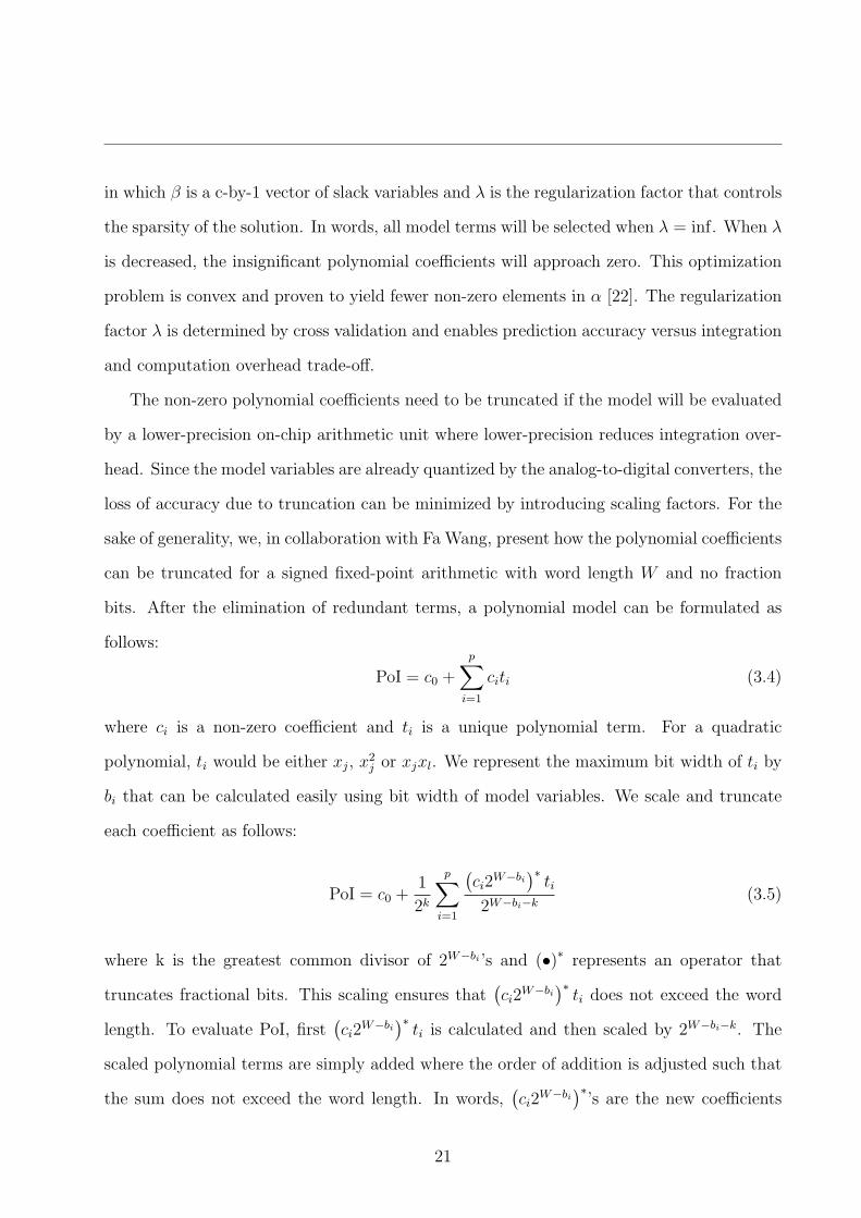
Figure 3.1: Self-healing using indirect performance sensor.
The polynomial model with reduced and truncated coefficients is evaluated using an
on-chip processing unit as shown in Figure 3.1. In a system-on-chip application a nearby
processing element can also be utilized for model evaluation reducing the area overhead.
Registers (REG) are used to store sensor outputs and nonvolatile memory (ROM) is used
to store model coefficients and the list of instructions that evaluate the model. In the ideal
case the indirect sensor model trained using circuit simulations is ready for self-healing. It
is possible, however, that the indirect sensor fails to predict the actual performance and
requires calibration during post-manufacturing tests as we mentioned earlier. In this case
22

the indirect sensor model can be calibrated by testing few dies from each wafer (to correct for
wafer-to-wafer variation) or by testing each individual die (to correct for die-to-die variation)
depending on the discrepancy between the simulated and measured behavior. A general
purpose processing unit allows such a calibration for immature process technologies (where
the mismatch between simulated or actual performance is high) or for advanced specifications
(which test the limits of the process technology). The calibrated sensor coefficients and
instructions can easily be scanned into the chips, as shown in Figure 3.1. In the following
sections we apply this methodology to indirect sensing of phase noise in VCO’s and frequency
characteristics of PLL’s.
3.2 Indirect Phase Noise Sensing
As previously mentioned in Chapter 2, phase noise quantifies the spectral purity of an
oscillator’s output and can be a demanding specification, particularly for high data-rate
wireless transceivers. Phase noise is defined as the ratio of noise power at a particular
frequency offset around the carrier frequency to total carrier power. Since the phase noise
at offset frequencies beyond the PLL bandwidth is dominated by the VCO, we focus on
self-healing of VCO phase noise. LC tank based VCO’s employ wide transistors with long
channel length to have sufficient gain and to reduce flicker noise. Such circuits are also laid
out carefully to reduce layout-dependent systematic process variations. As a result, the high
variation in phase noise we show in the following subsections is mainly due to temperature,
frequency and global process shifts.
Owing to its nonlinear and time varying nature, there does not exist a closed-form ana-
lytical expression for phase noise [23, 24]. A linear time invariant approximation for phase
noise in LC tank oscillators (a.k.a. the Leeson model [24]) is formulated as follows:
L ∆f = 10 log10
[
2FkT
PS
[
1 +
(
f02QL∆f
)2]
(
1 +f1/f3
|∆f |
)
]
(3.7)
23
in which ∆f is the offset frequency, F is an empirical noise factor, k is the Boltzmann’s
constant, T is the absolute temperature, PS is the carrier power in dBm, f0 is the carrier
frequency, QL is the quality factor of the tank and f1/f3 is flicker noise corner frequency. (3.7)
clearly shows that phase noise is related to temperature, frequency, VCO current and carrier
amplitude (A), which are easy to measure using integrated circuits making them good feature
candidates for indirect sensing. The phase noise tuning knob (tB) and the coarse frequency
tuning knob (kB) are also immediate feature candidates. Using these features the indirect
sensor model can be expressed as follows:
L ∆f = 10log10 [f (A, T, F, kB, tB)] (3.8)
where f (•) is a polynomial function. The oscillation amplitude can be measured by a peak
detector circuit similar to the one in [15] and the temperature can be measured by a thermal
sensor such as the one in [25].
In the following sections we apply indirect phase noise sensing for two different low-noise
VCO circuits: differential Colpitts VCO and linearized transconductance VCO. Based on
each indirect phase noise sensor, we also demonstrate a self-healing algorithm that minimizes
power dissipation while achieving a given phase noise target.
3.2.1 Differential Colpitts Oscillator
We applied indirect phase noise sensing to a 25GHz differential Colpitts VCO (VCODC)
implemented in 32nm CMOS SOI technology by Jean Olivier Plouchart at IBM. The differen-
tial Colpitts VCO, shown in Figure 3.2, achieves lower phase noise compared to conventional
cross-coupled VCO since the active devices deliver energy to the tank when the sensitiv-
ity to noise is minimum [26]. The low phase noise property makes the existing integrated
phase noise sensors impractical for self-healing. Therefore, we developed an indirect sensor
to predict phase noise at 10 MHz offset frequency.
24
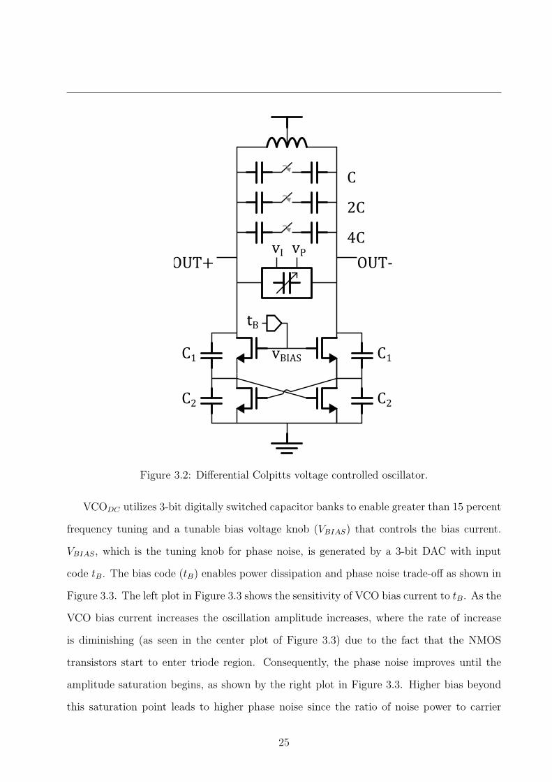
C
2C
4C
vBIAS
OUT+ OUT-
vI vP
tB
C1
C2
C1
C2
Figure 3.2: Differential Colpitts voltage controlled oscillator.
VCODC utilizes 3-bit digitally switched capacitor banks to enable greater than 15 percent
frequency tuning and a tunable bias voltage knob (VBIAS) that controls the bias current.
VBIAS, which is the tuning knob for phase noise, is generated by a 3-bit DAC with input
code tB. The bias code (tB) enables power dissipation and phase noise trade-off as shown in
Figure 3.3. The left plot in Figure 3.3 shows the sensitivity of VCO bias current to tB. As the
VCO bias current increases the oscillation amplitude increases, where the rate of increase
is diminishing (as seen in the center plot of Figure 3.3) due to the fact that the NMOS
transistors start to enter triode region. Consequently, the phase noise improves until the
amplitude saturation begins, as shown by the right plot in Figure 3.3. Higher bias beyond
this saturation point leads to higher phase noise since the ratio of noise power to carrier
25
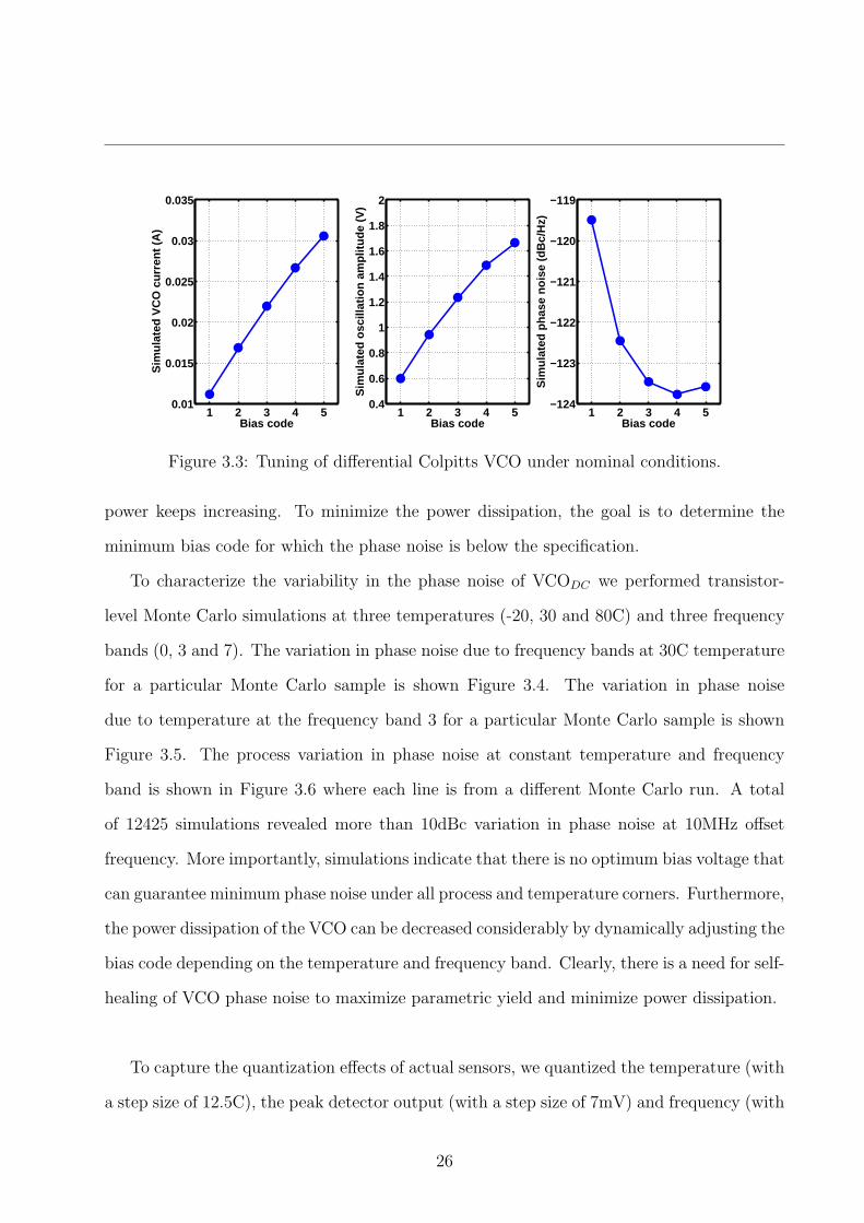
1 2 3 4 50.01
0.015
0.02
0.025
0.03
0.035
Bias code
Sim
ulat
ed V
CO
cur
rent
(A
)
1 2 3 4 50.4
0.6
0.8
1
1.2
1.4
1.6
1.8
2
Bias code
Sim
ulat
ed o
scill
atio
n am
plitu
de (
V)
1 2 3 4 5−124
−123
−122
−121
−120
−119
Bias code
Sim
ulat
ed p
hase
noi
se (
dBc/
Hz)
Figure 3.3: Tuning of differential Colpitts VCO under nominal conditions.
power keeps increasing. To minimize the power dissipation, the goal is to determine the
minimum bias code for which the phase noise is below the specification.
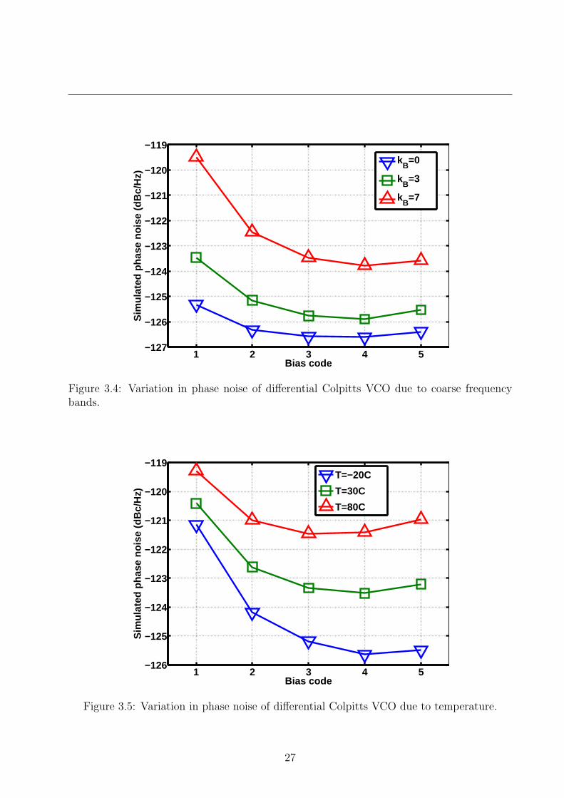
To characterize the variability in the phase noise of VCODC we performed transistor-
level Monte Carlo simulations at three temperatures (-20, 30 and 80C) and three frequency
bands (0, 3 and 7). The variation in phase noise due to frequency bands at 30C temperature
for a particular Monte Carlo sample is shown Figure 3.4. The variation in phase noise
due to temperature at the frequency band 3 for a particular Monte Carlo sample is shown
Figure 3.5. The process variation in phase noise at constant temperature and frequency
band is shown in Figure 3.6 where each line is from a different Monte Carlo run. A total
of 12425 simulations revealed more than 10dBc variation in phase noise at 10MHz offset
frequency. More importantly, simulations indicate that there is no optimum bias voltage that
can guarantee minimum phase noise under all process and temperature corners. Furthermore,
the power dissipation of the VCO can be decreased considerably by dynamically adjusting the
bias code depending on the temperature and frequency band. Clearly, there is a need for self-
healing of VCO phase noise to maximize parametric yield and minimize power dissipation.
To capture the quantization effects of actual sensors, we quantized the temperature (with
a step size of 12.5C), the peak detector output (with a step size of 7mV) and frequency (with
26
1 2 3 4 5−127
−126
−125
−124
−123
−122
−121
−120
−119
Bias code
Sim
ulat
ed p
hase
noi
se (
dBc/
Hz)
kB
=0
kB
=3
kB
=7
Figure 3.4: Variation in phase noise of differential Colpitts VCO due to coarse frequencybands.
1 2 3 4 5−126
−125
−124
−123
−122
−121
−120
−119
Bias code
Sim
ulat
ed p
hase
noi
se (
dBc/
Hz)
T=−20C
T=30C
T=80C
Figure 3.5: Variation in phase noise of differential Colpitts VCO due to temperature.
27

1 2 3 4 5−123
−122
−121
−120
−119
−118
−117
Bias code
Sim
ulat
ed p
hase
noi
se (
dBc/
Hz)
Sample#1Sample#2Sample#3Sample#4
Figure 3.6: Variation in phase noise of differential Colpitts VCO due to process.
a step size of 32MHz) in binary form. The frequency band (kB) and bias code (tB) are al-
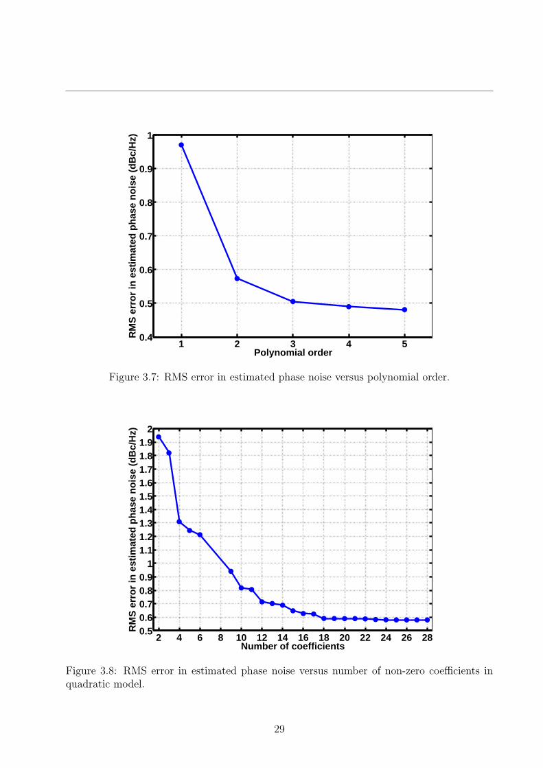
ready quantized. We determined the order of polynomial in (3.8) by 10-fold cross-validation.
The rms error between the simulated phase noise and the phase noise estimated by indirect
sensor is shown in Figure 3.7 for varying model order. Figure 3.7 shows that there is a
negligible improvement in sensor accuracy beyond quadratic approximation. We then ap-
plied the L1-norm regularization technique formulated in (3.3) to eliminate the redundant
polynomial terms. The rms error between the simulated phase noise and the phase noise
estimated by indirect sensor is presented in Figure 3.8 for varying number of non-zero poly-
nomial coefficients. Figure 3.8 shows that as many as 10 terms can be discarded with less
than 0.1 dBc/Hz degradation in prediction accuracy. Based on this analysis, we trained a
quadratic indirect phase noise sensor with 18 non-zero coefficients that achieves an rms error
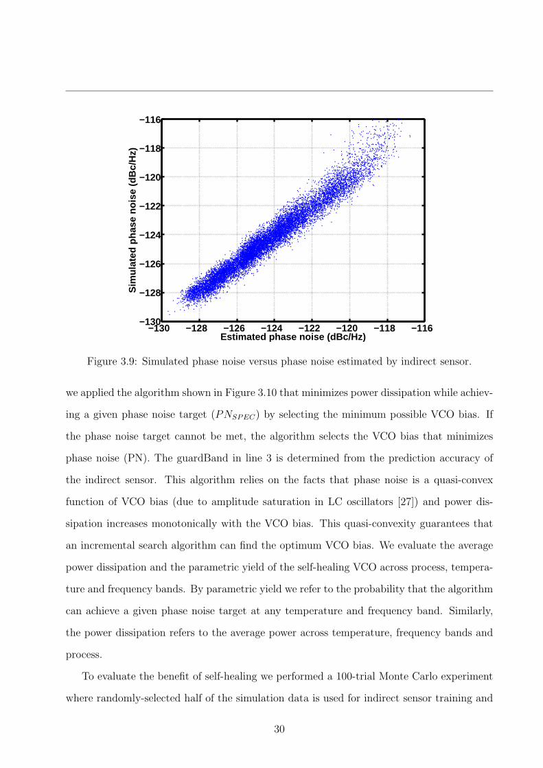
of 0.6dBc/Hz. Figure 3.9 compares the phase noise predicted by this indirect sensor with
the simulated phase noise for randomly generated validation sets showing a high correlation
between the two.
To demonstrate the applicability of indirect phase noise sensing for self-healing VCODC
28
1 2 3 4 50.4
0.5
0.6
0.7
0.8
0.9
1
Polynomial order
RM
S e
rror
in e
stim
ated
pha
se n
oise
(dB
c/H
z)
Figure 3.7: RMS error in estimated phase noise versus polynomial order.
2 4 6 8 10 12 14 16 18 20 22 24 26 280.50.60.70.80.9
11.11.21.31.41.51.61.71.81.9
2
Number of coefficients
RM
S e
rror
in e
stim
ated
pha
se n
oise
(dB
c/H
z)
Figure 3.8: RMS error in estimated phase noise versus number of non-zero coefficients inquadratic model.
29
−130 −128 −126 −124 −122 −120 −118 −116−130
−128
−126
−124
−122
−120
−118
−116
Estimated phase noise (dBc/Hz)
Sim
ulat
ed p
hase
noi
se (
dBc/
Hz)
Figure 3.9: Simulated phase noise versus phase noise estimated by indirect sensor.
we applied the algorithm shown in Figure 3.10 that minimizes power dissipation while achiev-
ing a given phase noise target (PNSPEC) by selecting the minimum possible VCO bias. If
the phase noise target cannot be met, the algorithm selects the VCO bias that minimizes
phase noise (PN). The guardBand in line 3 is determined from the prediction accuracy of
the indirect sensor. This algorithm relies on the facts that phase noise is a quasi-convex
function of VCO bias (due to amplitude saturation in LC oscillators [27]) and power dis-
sipation increases monotonically with the VCO bias. This quasi-convexity guarantees that
an incremental search algorithm can find the optimum VCO bias. We evaluate the average
power dissipation and the parametric yield of the self-healing VCO across process, tempera-
ture and frequency bands. By parametric yield we refer to the probability that the algorithm
can achieve a given phase noise target at any temperature and frequency band. Similarly,
the power dissipation refers to the average power across temperature, frequency bands and
process.
To evaluate the benefit of self-healing we performed a 100-trial Monte Carlo experiment
where randomly-selected half of the simulation data is used for indirect sensor training and
30

the other half is used to compute parametric yield and power dissipation in each trial. We
compared the self-healing VCO against the following approaches:
• Ideal self-healing is an unrealizable algorithm that employs an ideal phase noise sen-
sor and, therefore, can determine the best achievable phase noise and the minimum bias
voltage to achieve target phase-noise. Ideal self-healing represents the upper bound on
parametric yield and the corresponding lower bound on the average power dissipation
for any phase noise target.
• No self-healing represents a design without any tuning capabilities and always uti-
lizes a fixed VCO bias. As it is difficult to determine the optimal bias code before
manufacturing, we consider no self-healing for each bias voltage.
MINIMUM POWER BIASING
1 Initialization: tB ← tB,MIN , PNMIN ←∞ and wait for stabilization2 Measure the temperature using a thermal sensor3 while (PNMIN + guardBand > PNSPEC) and (tB < tB,MAX)
do
4 Measure the free-running oscillation frequency using a counter5 Measure the amplitude using a peak detector6 Estimate phase noise (PN) using indirect sensor7 if (PN < PNMIN)
then
8 PNMIN ← PN9 tB ← tB + 1
else
10 tB ← tB − 111 Terminate
Figure 3.10: Self-healing algorithm for VCO phase noise.
Figure 3.11 presents the simulated parametric yield achieved by ideal self-healing, non-
healing and self-healing by indirect sensor for varying phase noise target. This figure shows
that the parametric yield of self-healing is very close to the maximum achievable yield. On
the other hand, non-healing design may result in significant yield loss for tB = 1, 2 and
31
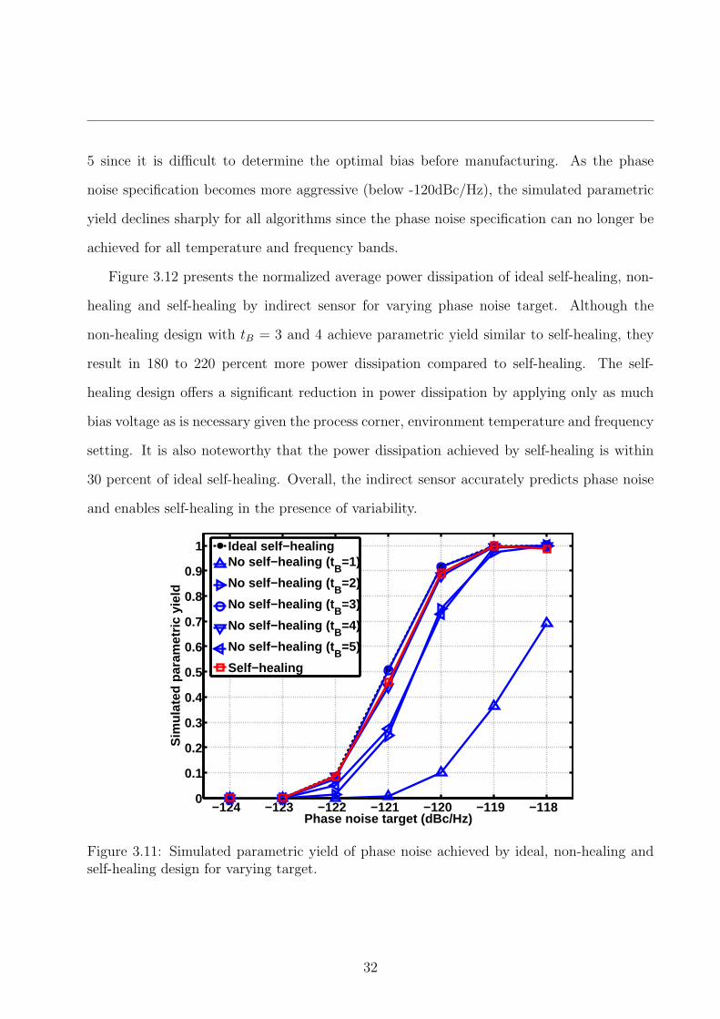
5 since it is difficult to determine the optimal bias before manufacturing. As the phase
noise specification becomes more aggressive (below -120dBc/Hz), the simulated parametric
yield declines sharply for all algorithms since the phase noise specification can no longer be
achieved for all temperature and frequency bands.
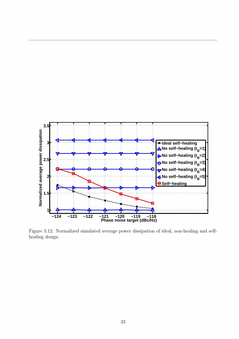
Figure 3.12 presents the normalized average power dissipation of ideal self-healing, non-
healing and self-healing by indirect sensor for varying phase noise target. Although the
non-healing design with tB = 3 and 4 achieve parametric yield similar to self-healing, they
result in 180 to 220 percent more power dissipation compared to self-healing. The self-
healing design offers a significant reduction in power dissipation by applying only as much
bias voltage as is necessary given the process corner, environment temperature and frequency
setting. It is also noteworthy that the power dissipation achieved by self-healing is within
30 percent of ideal self-healing. Overall, the indirect sensor accurately predicts phase noise
and enables self-healing in the presence of variability.
−124 −123 −122 −121 −120 −119 −1180
0.1
0.2
0.3
0.4
0.5
0.6
0.7
0.8
0.9
1
Phase noise target (dBc/Hz)
Sim
ulat
ed p
aram
etric
yie
ld
Ideal self−healingNo self−healing (t
B=1)
No self−healing (tB
=2)
No self−healing (tB
=3)
No self−healing (tB
=4)
No self−healing (tB
=5)
Self−healing
Figure 3.11: Simulated parametric yield of phase noise achieved by ideal, non-healing andself-healing design for varying target.
32
−124 −123 −122 −121 −120 −119 −1181
1.5
2
2.5
3
3.5
Phase noise target (dBc/Hz)
Nor
mal
ized
ave
rage
pow
er d
issi
patio
n
Ideal self−healingNo self−healing (t
B=1)
No self−healing (tB
=2)
No self−healing (tB
=3)
No self−healing (tB
=4)
No self−healing (tB
=5)
Self−healing
Figure 3.12: Normalized simulated average power dissipation of ideal, non-healing and self-healing design.
33
3.2.2 Linearized Transconductance Oscillator
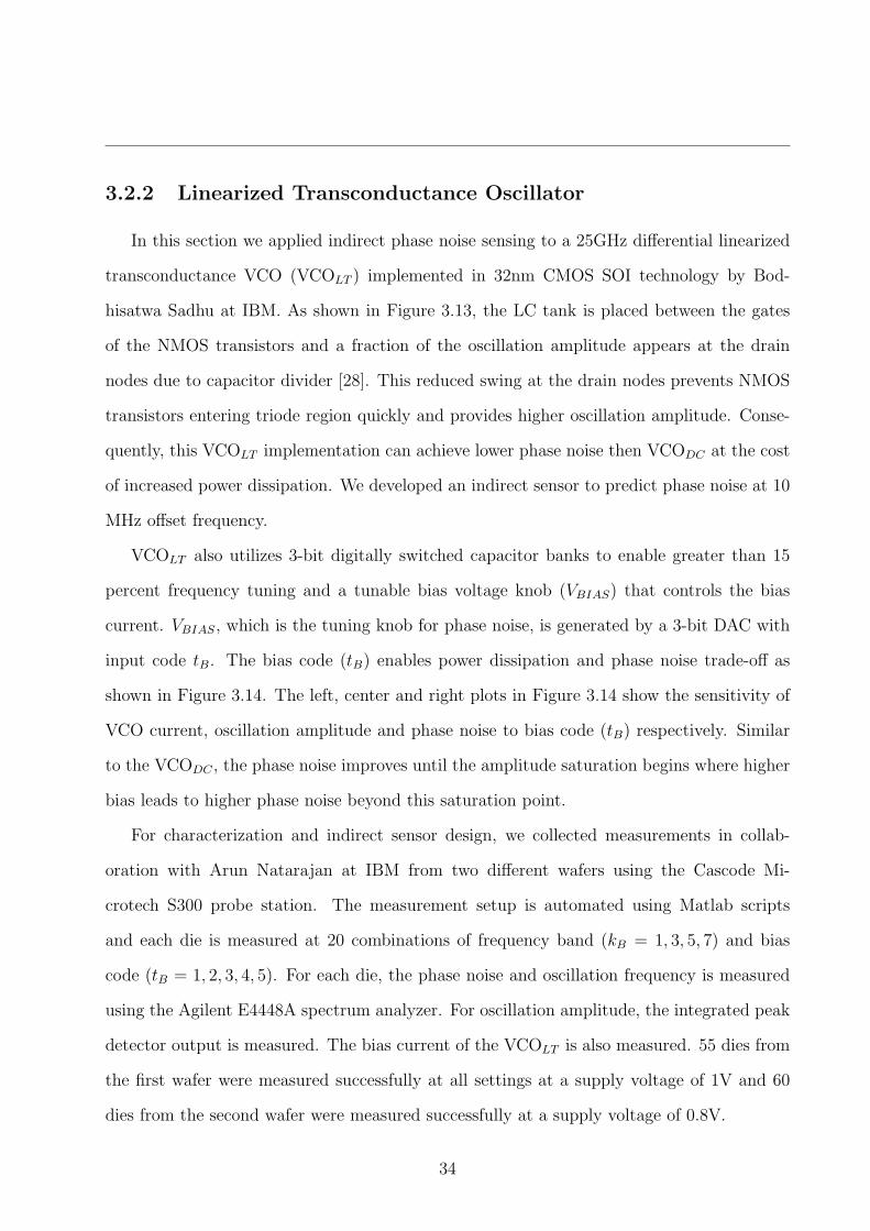
In this section we applied indirect phase noise sensing to a 25GHz differential linearized
transconductance VCO (VCOLT ) implemented in 32nm CMOS SOI technology by Bod-
hisatwa Sadhu at IBM. As shown in Figure 3.13, the LC tank is placed between the gates
of the NMOS transistors and a fraction of the oscillation amplitude appears at the drain
nodes due to capacitor divider [28]. This reduced swing at the drain nodes prevents NMOS
transistors entering triode region quickly and provides higher oscillation amplitude. Conse-
quently, this VCOLT implementation can achieve lower phase noise then VCODC at the cost
of increased power dissipation. We developed an indirect sensor to predict phase noise at 10
MHz offset frequency.
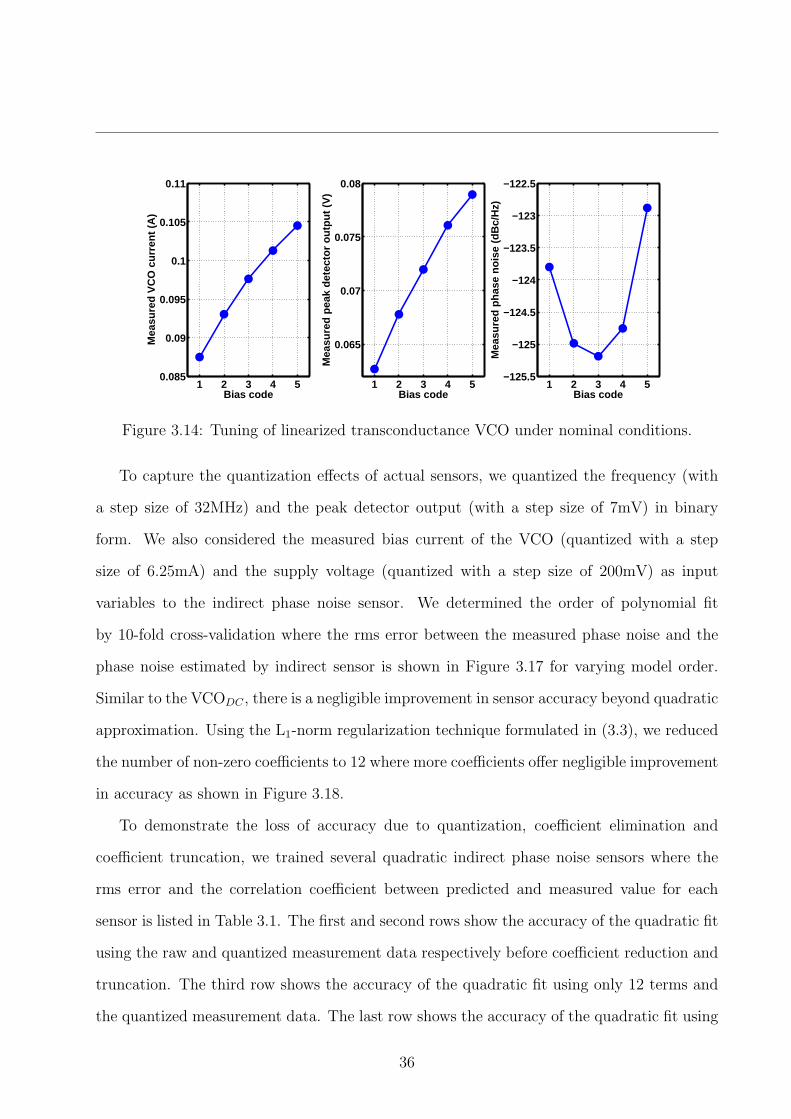
VCOLT also utilizes 3-bit digitally switched capacitor banks to enable greater than 15
percent frequency tuning and a tunable bias voltage knob (VBIAS) that controls the bias
current. VBIAS, which is the tuning knob for phase noise, is generated by a 3-bit DAC with
input code tB. The bias code (tB) enables power dissipation and phase noise trade-off as
shown in Figure 3.14. The left, center and right plots in Figure 3.14 show the sensitivity of
VCO current, oscillation amplitude and phase noise to bias code (tB) respectively. Similar
to the VCODC , the phase noise improves until the amplitude saturation begins where higher
bias leads to higher phase noise beyond this saturation point.
For characterization and indirect sensor design, we collected measurements in collab-
oration with Arun Natarajan at IBM from two different wafers using the Cascode Mi-
crotech S300 probe station. The measurement setup is automated using Matlab scripts
and each die is measured at 20 combinations of frequency band (kB = 1, 3, 5, 7) and bias
code (tB = 1, 2, 3, 4, 5). For each die, the phase noise and oscillation frequency is measured
using the Agilent E4448A spectrum analyzer. For oscillation amplitude, the integrated peak
detector output is measured. The bias current of the VCOLT is also measured. 55 dies from
the first wafer were measured successfully at all settings at a supply voltage of 1V and 60
dies from the second wafer were measured successfully at a supply voltage of 0.8V.
34

vBIAS
C
2C
4C
OUT+ OUT-
vI vP
Cc Cc
Cd Cd
tB
Figure 3.13: Linearized transconductance VCO.
The variation in phase noise due to frequency bands for a particular die is shown Fig-
ure 3.15. The process variation in phase noise at constant frequency band is shown in
Figure 3.16, where each line is from a different die. Similar to the VCODC , there does not
exist an optimum bias voltage that can guarantee minimum phase noise for all dies and at all
frequency bands. A total of 2300 measurements revealed approximately 10.8dBc variation
in phase noise at 10MHz offset frequency. The standard deviation of die-to-die variation in
phase noise at constant bias (tB = 3) and constant frequency band (kB = 5) in the first (sec-
ond) wafer is 0.45 (0.51) dBc/Hz. Measurements for varying temperature were attempted
but could not be completed due to wear out of contact probes.
35
1 2 3 4 50.085
0.09
0.095
0.1
0.105
0.11
Bias code
Mea
sure
d V
CO
cur
rent
(A
)
1 2 3 4 5
0.065
0.07
0.075
0.08
Bias code
Mea
sure
d pe
ak d
etec
tor
outp
ut (
V)
1 2 3 4 5−125.5
−125
−124.5
−124
−123.5
−123
−122.5
Bias code
Mea
sure
d ph
ase
nois
e (d
Bc/
Hz)
Figure 3.14: Tuning of linearized transconductance VCO under nominal conditions.
To capture the quantization effects of actual sensors, we quantized the frequency (with
a step size of 32MHz) and the peak detector output (with a step size of 7mV) in binary
form. We also considered the measured bias current of the VCO (quantized with a step
size of 6.25mA) and the supply voltage (quantized with a step size of 200mV) as input
variables to the indirect phase noise sensor. We determined the order of polynomial fit
by 10-fold cross-validation where the rms error between the measured phase noise and the
phase noise estimated by indirect sensor is shown in Figure 3.17 for varying model order.
Similar to the VCODC , there is a negligible improvement in sensor accuracy beyond quadratic
approximation. Using the L1-norm regularization technique formulated in (3.3), we reduced
the number of non-zero coefficients to 12 where more coefficients offer negligible improvement
in accuracy as shown in Figure 3.18.
To demonstrate the loss of accuracy due to quantization, coefficient elimination and
coefficient truncation, we trained several quadratic indirect phase noise sensors where the
rms error and the correlation coefficient between predicted and measured value for each
sensor is listed in Table 3.1. The first and second rows show the accuracy of the quadratic fit
using the raw and quantized measurement data respectively before coefficient reduction and
truncation. The third row shows the accuracy of the quadratic fit using only 12 terms and
the quantized measurement data. The last row shows the accuracy of the quadratic fit using
36

1 2 3 4 5−127
−126
−125
−124
−123
−122
−121
−120
Bias code
Mea
sure
d ph
ase
nois
e (d
Bc/
Hz)
kB
=1
kB
=3
kB
=5
kB
=7
Figure 3.15: Variation in phase noise of linearized transconductance VCO due to coarsefrequency bands.
1 2 3 4 5−126.5
−126
−125.5
−125
−124.5
−124
−123.5
−123
Bias code
Mea
sure
d ph
ase
nois
e (d
Bc/
Hz)
Sample#1Sample#2Sample#3Sample#4
Figure 3.16: Variation in phase noise of linearized transconductance VCO due to process.
37
quantized measurement data, coefficient elimination and truncation for 16-bit arithmetic.
This last row represents the accuracy of the indirect sensor model that is ready for on-chip
integration. Table 3.1 shows that the finalized indirect sensor can still accurately predict the
phase noise.
Table 3.1: Indirect phase noise sensor accuracyRms error Correlation(dBc/Hz) Coefficient
Raw data with full coefficients 0.66 0.94Quantized data 0.67 0.94Quantized data, reduced coefficients 0.71 0.93Quantized data, reduced and truncated coefficients 0.77 0.92
To demonstrate the applicability of indirect phase noise sensing for self-healing VCODC
we applied the algorithm in Figure 3.10 that minimizes power dissipation while achieving a
given phase noise target using the indirect sensor ready for on-chip integration. Due to the
limited number of measurements, we used all of the measurement data for sensor training
and algorithm evaluation.
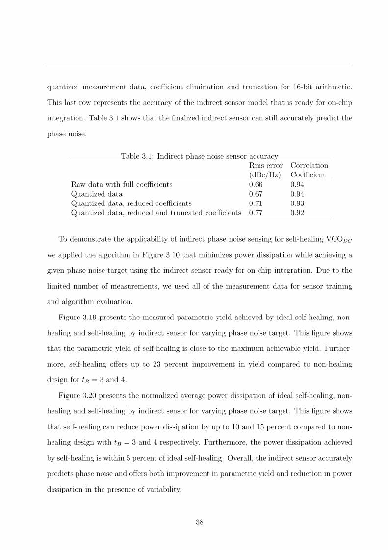
Figure 3.19 presents the measured parametric yield achieved by ideal self-healing, non-
healing and self-healing by indirect sensor for varying phase noise target. This figure shows
that the parametric yield of self-healing is close to the maximum achievable yield. Further-
more, self-healing offers up to 23 percent improvement in yield compared to non-healing
design for tB = 3 and 4.
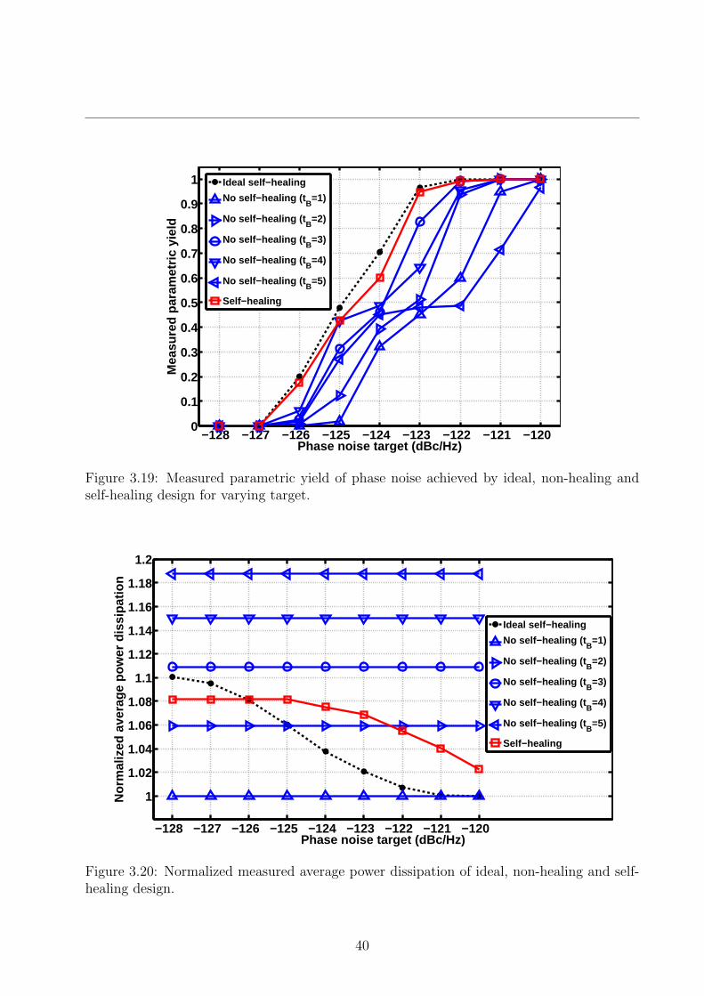
Figure 3.20 presents the normalized average power dissipation of ideal self-healing, non-
healing and self-healing by indirect sensor for varying phase noise target. This figure shows
that self-healing can reduce power dissipation by up to 10 and 15 percent compared to non-
healing design with tB = 3 and 4 respectively. Furthermore, the power dissipation achieved
by self-healing is within 5 percent of ideal self-healing. Overall, the indirect sensor accurately
predicts phase noise and offers both improvement in parametric yield and reduction in power
dissipation in the presence of variability.
38

1 2 3 40.4
0.6
0.8
1
1.2
1.4
Polynomial order
RM
S e
rror
in e
stim
ated
pha
se n
oise
(dB
c/H
z)
Figure 3.17: RMS error in estimated phase noise versus polynomial order.
2 4 6 8 10 12 14 16 18 20 22 24 26 280.50.60.70.80.9
11.11.21.31.41.51.61.71.81.9
2
Number of coefficients
RM
S e
rror
in e
stim
ated
pha
se n
oise
(dB
c/H
z)
Figure 3.18: RMS error in estimated phase noise versus number of non-zero coefficients inquadratic model.
39
−128 −127 −126 −125 −124 −123 −122 −121 −1200
0.1
0.2
0.3
0.4
0.5
0.6
0.7
0.8
0.9
1
Phase noise target (dBc/Hz)
Mea
sure
d pa
ram
etric
yie
ld
Ideal self−healing
No self−healing (tB
=1)
No self−healing (tB
=2)
No self−healing (tB
=3)
No self−healing (tB
=4)
No self−healing (tB
=5)
Self−healing
Figure 3.19: Measured parametric yield of phase noise achieved by ideal, non-healing andself-healing design for varying target.
−128 −127 −126 −125 −124 −123 −122 −121 −120
1
1.02
1.04
1.06
1.08
1.1
1.12
1.14
1.16
1.18
1.2
Phase noise target (dBc/Hz)
Nor
mal
ized
ave
rage
pow
er d
issi
patio
n
Ideal self−healing
No self−healing (tB
=1)
No self−healing (tB
=2)
No self−healing (tB
=3)
No self−healing (tB
=4)
No self−healing (tB
=5)
Self−healing
Figure 3.20: Normalized measured average power dissipation of ideal, non-healing and self-healing design.
40
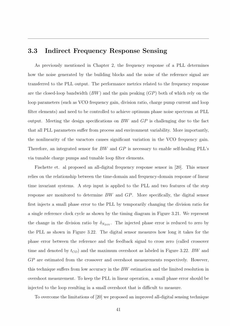
3.3 Indirect Frequency Response Sensing
As previously mentioned in Chapter 2, the frequency response of a PLL determines
how the noise generated by the building blocks and the noise of the reference signal are
transferred to the PLL output. The performance metrics related to the frequency response
are the closed-loop bandwidth (BW ) and the gain peaking (GP ) both of which rely on the
loop parameters (such as VCO frequency gain, division ratio, charge pump current and loop
filter elements) and need to be controlled to achieve optimum phase noise spectrum at PLL
output. Meeting the design specifications on BW and GP is challenging due to the fact
that all PLL parameters suffer from process and environment variability. More importantly,
the nonlinearity of the varactors causes significant variation in the VCO frequency gain.
Therefore, an integrated sensor for BW and GP is necessary to enable self-healing PLL’s
via tunable charge pumps and tunable loop filter elements.
Fischette et. al proposed an all-digital frequency response sensor in [20]. This sensor
relies on the relationship between the time-domain and frequency-domain response of linear
time invariant systems. A step input is applied to the PLL and two features of the step
response are monitored to determine BW and GP . More specifically, the digital sensor
first injects a small phase error to the PLL by temporarily changing the division ratio for
a single reference clock cycle as shown by the timing diagram in Figure 3.21. We represent
the change in the division ratio by δNDIV. The injected phase error is reduced to zero by
the PLL as shown in Figure 3.22. The digital sensor measures how long it takes for the
phase error between the reference and the feedback signal to cross zero (called crossover
time and denoted by tCO) and the maximum overshoot as labeled in Figure 3.22. BW and
GP are estimated from the crossover and overshoot measurements respectively. However,
this technique suffers from low accuracy in the BW estimation and the limited resolution in
overshoot measurement. To keep the PLL in linear operation, a small phase error should be
injected to the loop resulting in a small overshoot that is difficult to measure.
To overcome the limitations of [20] we proposed an improved all-digital sensing technique
41

1 2 3 .. .. N1 1 2 3 .. .. N2.. 1 2 3 .. .. N1
REF
VCO
NDIVN1 N2 N1
FB
Figure 3.21: Phase error injection by temporary change in division ratio.
0 20 40 60 80 100−0.2
0
0.2
0.4
0.6
0.8
1
Number of reference clock cycles
Nor
mal
ized
pha
se e
rror
crossover
overshoot
Figure 3.22: Crossover and overshoot measurement in prior work.
without overshoot measurements in collaboration with Arun Natarajan and Mark Ferriss at
IBM. In our technique, a small phase error is injected repetitively after each crossover as
shown in Figure 3.23 and the crossover times are measured by digital counters. BW and
GP are predicted as a polynomial function of multiple crossover times as follows:
BW =1
fBW (tCO1, .., tCOk
)(3.9)
GP =1
fGP (tCO1, .., tCOk
)(3.10)
where tCOidenotes the ith crossover measurement. fBW (•) and fGP (•) are obtained using
42
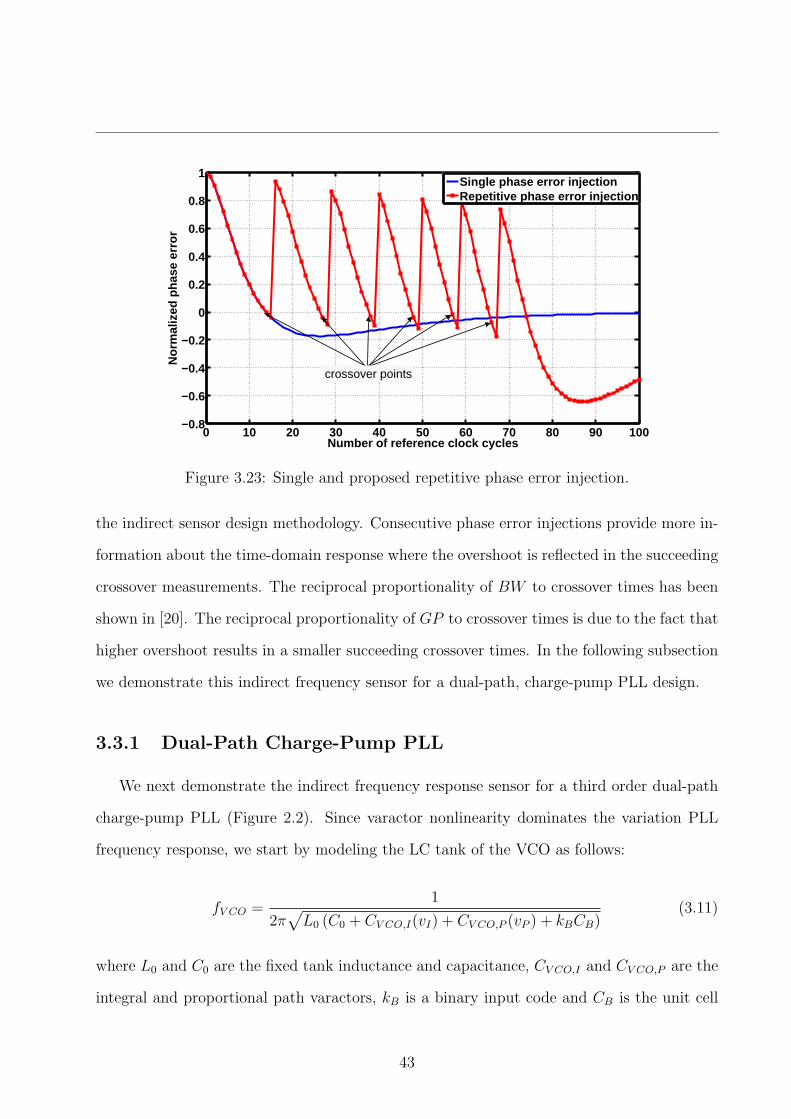
0 10 20 30 40 50 60 70 80 90 100−0.8
−0.6
−0.4
−0.2
0
0.2
0.4
0.6
0.8
1
Number of reference clock cycles
Nor
mal
ized
pha
se e
rror
Single phase error injectionRepetitive phase error injection
crossover points
Figure 3.23: Single and proposed repetitive phase error injection.
the indirect sensor design methodology. Consecutive phase error injections provide more in-
formation about the time-domain response where the overshoot is reflected in the succeeding
crossover measurements. The reciprocal proportionality of BW to crossover times has been
shown in [20]. The reciprocal proportionality of GP to crossover times is due to the fact that
higher overshoot results in a smaller succeeding crossover times. In the following subsection
we demonstrate this indirect frequency sensor for a dual-path, charge-pump PLL design.
3.3.1 Dual-Path Charge-Pump PLL
We next demonstrate the indirect frequency response sensor for a third order dual-path
charge-pump PLL (Figure 2.2). Since varactor nonlinearity dominates the variation PLL
frequency response, we start by modeling the LC tank of the VCO as follows:
fV CO =1
2π√
L0 (C0 + CV CO,I(vI) + CV CO,P (vP ) + kBCB)(3.11)
where L0 and C0 are the fixed tank inductance and capacitance, CV CO,I and CV CO,P are the
integral and proportional path varactors, kB is a binary input code and CB is the unit cell
43
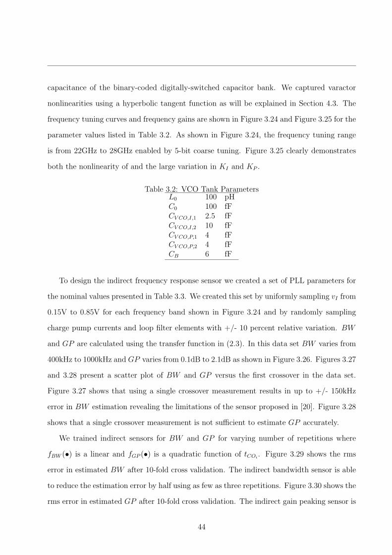
capacitance of the binary-coded digitally-switched capacitor bank. We captured varactor
nonlinearities using a hyperbolic tangent function as will be explained in Section 4.3. The
frequency tuning curves and frequency gains are shown in Figure 3.24 and Figure 3.25 for the
parameter values listed in Table 3.2. As shown in Figure 3.24, the frequency tuning range
is from 22GHz to 28GHz enabled by 5-bit coarse tuning. Figure 3.25 clearly demonstrates
both the nonlinearity of and the large variation in KI and KP .
Table 3.2: VCO Tank ParametersL0 100 pHC0 100 fFCV CO,I,1 2.5 fFCV CO,I,2 10 fFCV CO,P,1 4 fFCV CO,P,2 4 fFCB 6 fF
To design the indirect frequency response sensor we created a set of PLL parameters for
the nominal values presented in Table 3.3. We created this set by uniformly sampling vI from
0.15V to 0.85V for each frequency band shown in Figure 3.24 and by randomly sampling
charge pump currents and loop filter elements with +/- 10 percent relative variation. BW
and GP are calculated using the transfer function in (2.3). In this data set BW varies from
400kHz to 1000kHz and GP varies from 0.1dB to 2.1dB as shown in Figure 3.26. Figures 3.27
and 3.28 present a scatter plot of BW and GP versus the first crossover in the data set.
Figure 3.27 shows that using a single crossover measurement results in up to +/- 150kHz
error in BW estimation revealing the limitations of the sensor proposed in [20]. Figure 3.28
shows that a single crossover measurement is not sufficient to estimate GP accurately.
We trained indirect sensors for BW and GP for varying number of repetitions where
fBW (•) is a linear and fGP (•) is a quadratic function of tCOi. Figure 3.29 shows the rms
error in estimated BW after 10-fold cross validation. The indirect bandwidth sensor is able
to reduce the estimation error by half using as few as three repetitions. Figure 3.30 shows the
rms error in estimated GP after 10-fold cross validation. The indirect gain peaking sensor is
44
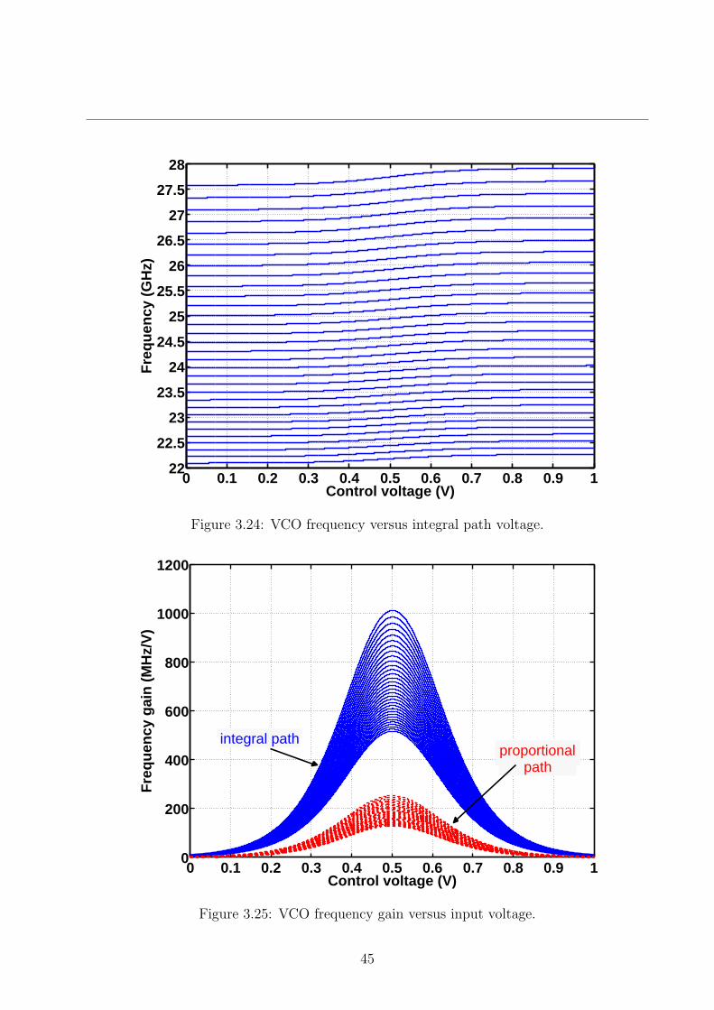
0 0.1 0.2 0.3 0.4 0.5 0.6 0.7 0.8 0.9 122
22.5
23
23.5
24
24.5
25
25.5
26
26.5
27
27.5
28F
requ
ency
(G
Hz)
Control voltage (V)
Figure 3.24: VCO frequency versus integral path voltage.
0 0.1 0.2 0.3 0.4 0.5 0.6 0.7 0.8 0.9 10
200
400
600
800
1000
1200
Fre
quen
cy g
ain
(MH
z/V
)
Control voltage (V)
integral pathproportional
path
Figure 3.25: VCO frequency gain versus input voltage.
45

able to reduce the estimation error below half a dB using as few as four repetitions. Overall,
the indirect sensing applied to frequency response of PLL’s offers significant improvement in
accuracy.
Table 3.3: PLL parameters and metricsfREF 24.95 MHz fUGF 500 kHzNDIV 1000 — PM 62 degreeskB 13 — BW 767 kHzKI 736 MHz/V GP 1.57 dBKP 184 MHz/VII 53 µAIP 636 µACI 15 .9 pFCP 3.18 pFRP 25 kΩτPFD 50 psec
400 500 600 700 800 900 10000
0.5
1
1.5
2
2.5
Bandwidth (kHz)
Gai
n pe
akin
g (d
B)
Figure 3.26: Gain peaking versus bandwidth in the simulated data.
46
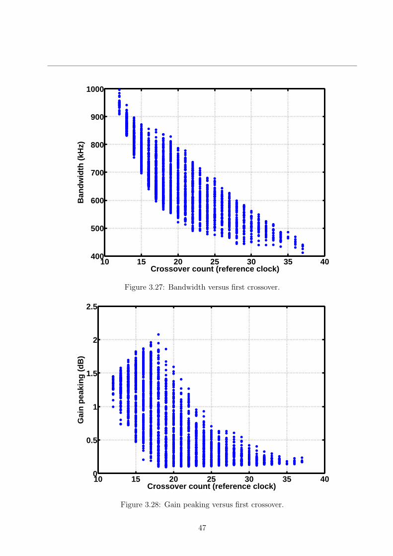
10 15 20 25 30 35 40400
500
600
700
800
900
1000B
andw
idth
(kH
z)
Crossover count (reference clock)
Figure 3.27: Bandwidth versus first crossover.
10 15 20 25 30 35 400
0.5
1
1.5
2
2.5
Gai
n pe
akin
g (d
B)
Crossover count (reference clock)
Figure 3.28: Gain peaking versus first crossover.
47

1 2 3 4 525
30
35
40
45
50
55
60
65
Number of phase error injections
RM
S e
rror
in e
stim
ated
ban
dwid
th (
kHz)
Figure 3.29: Accuracy of indirect bandwidth sensor for varying number of repetitions.
1 2 3 4 5
0.4
0.6
0.8
1
1.2
1.4
1.6
Number of phase error injections
RM
S e
rror
in e
stim
ated
gai
n pe
akin
g (d
B)
Figure 3.30: Accuracy of indirect gain peaking sensor for varying number of repetitions.
48

3.4 Summary
In this chapter we proposed and demonstrated a design methodology for indirect sensing
of performance metrics that are not easily measured on-chip either due to high integration
overhead or physical limitations. We first demonstrated indirect phase noise sensing for
two different VCO architectures using simulated and measured results. We showed self-
healing using indirect phase noise sensing can improve the parametric yield and reduce
power dissipation. Secondly, we demonstrated indirect bandwidth and gain peaking sensors
for PLL’s. We extended an existing all-digital bandwidth sensor by a new technique which
significantly improves sensor accuracy. In the following chapter we will focus on verification
of self-healing systems with both direct and indirect sensors.
49

Chapter 4
Verification of Self-Healing Systems
As stated in Chapter 1 we use the term verification to refer to performance validation
of analog circuits before manufacturing. The goal of verification is to determine whether
(and with what probability) the circuit meets design specifications under varying process,
environment and operating modes. Self-healing design makes verification more difficult com-
pared to conventional design by increasing circuit complexity and by bringing new issues to
consider. First, state of art verification methods cannot be used for tunable circuits directly
since it is impractical to simulate the circuit over the whole tuning range (excluding the
trivial scenarios where the circuit has few unique configurations to verify). In addition to
the tunable circuit, the accuracy of performance sensors should be verified. Furthermore, the
self-healing algorithm, which is a discrete-time feedback loop, should be stable and converge
to a feasible state in the presence of variability.
In this chapter we identify the challenges in verification of self-healing systems and present
general principles and methods to address these challenges. We begin with an overview of
state-of-art analog circuit verification in Section 4.1. In Sections 4.2, 4.3 and 4.4 we discuss
the verification of actuation, sensor and algorithm respectively with relevant circuit examples.
50
4.1 Overview of Analog Verification
The most accurate way to evaluate performance is circuit simulation that refers to the
numerical simulation of the device models provided by the integrated circuit foundry. The
circuit is typically placed in a testbench with appropriate input driver and output load
and simulated for different analyses. For example, transient analysis and AC analysis are
used to determine the large-signal characteristics and the small-signal frequency response of
amplifiers. The performance metric is typically expressed as an analytical function of the
time domain or frequency domain responses and compared against the specification.
Variability due to temperature or supply voltage can be analyzed using parametric simu-
lation where the circuit is simulated for a range or extreme values of given parameter values.
Effects of process variability has been analyzed by simulating the circuit at different process
corners that represent a carefully selected set of extreme conditions that can occur during
manufacturing. Due to the limitations of this corner-based approach in nanoscale CMOS
technologies, Monte Carlo circuit simulation (MCCS) is being widely adopted. MCCS is a
statistical technique where the circuit is simulated for a set of randomly generated samples
of process variables that represent systematic and random sources of variability during man-
ufacturing. MCCS provides an estimate of the probability distribution of each performance
metric that can be used to determine the probability of meeting the corresponding specifi-
cation. The variance of the estimated probability is inversely proportional to the number of
samples where the number of samples increases the simulation cost.
Although circuit simulation is the most accurate performance verification method for
analog and RF circuits, its runtime can be prohibitive for stiff, large-scale or self-healing
circuits. A stiff circuit example is the PLL where the VCO signal and the reference signal
can be order(s) of magnitude apart. In a transient analysis of a PLL, the time step is limited
by the VCO signal period while phase locking takes hundreds of reference clock periods. As
a result, the circuit simulation can take weeks for a PLL with a high division ratio. Similarly,
circuit simulation cost is too high for transmitter and receiver circuits due to increased circuit
51
size in addition to stiffness. SHD further exacerbates the verification problem by increasing
design complexity and by the addition of tunability. In a SHD with multiple tuning knobs,
brute-force circuit simulation for each tuning knob assignment can easily become impractical.
When circuit simulation is impractical for performance verification, a common way is to
employ higher-level abstractions also known as macromodels or behavioral models of system
components. A behavioral model is a simplified representation of a circuit that is expected
to provide the same or similar input output relationship. Behavioral models are trained by
circuit simulation with appropriate input drivers and output loads. These behavioral models
can either be used in behavioral simulation of larger systems offering significant speed up
compared to circuit simulation or can enable formal techniques that provide guarantees on
the performance.
The level of abstraction is critical during behavioral model generation and creates a trade
off between accuracy and complexity. An overly simplified model may cause optimistic re-
sults or may fail to capture possible errors in the actual system. On the other hand, an
overly conservative and detailed behavioral model can make formal techniques inapplicable
or increase the behavioral simulation time. State of the art modeling tools for analog cir-
cuits include Verilog-AMS and Matlab/Simulink [29, 30]. Analog behavioral modeling and
simulation has been widely used for PLL’s and communication circuits for early-stage de-
sign space exploration. Behavioral simulation can also be used for performance verification
by refining the accuracy of behavioral models or in a mixed approach where both device
models and behavioral models can be simulated in the same testbench. In the following sec-
tions we demonstrate how behavioral modeling and simulation can be used for verification
of self-healing systems. In Chapter 5 we focus on formal verification techniques and their
applicability for self-healing systems.
52
4.2 Actuation
In a self-healing system we are no longer interested in the performance of a circuit for
a particular tuning knob value, but we are interested in the sensitivity of performance to
tuning knob(s). More specifically, we would like to estimate the probability of whether there
is a feasible assignment to tuning knobs such that the circuit meets the design specifications
in the presence of process variability. This probability estimate is needed to determine
whether the tunable circuit provides sufficient actuation range and resolution for self-healing.
Furthermore, this probability is also an upper bound on the efficacy of any self-healing
algorithm.
A tunable circuit can be verified using Monte Carlo circuit simulation if the simulation
time is manageable. If PoI is a linear or monotonic function of the tuning knobs, then
tunability can be verified by running the Monte Carlo simulation for extreme points of
the actuation range. For example, a VCO should provide sufficient output power for the
following divider stages to function properly. The output power of the VCO design in
Figure 3.2 is a monotonic function of the bias voltage as shown in Figure 3.3. By exploiting
this monotonicity, we can determine the worst-case output power by simply simulating the
VCO for maximum bias voltage that provides the highest output power. Another relevant
example is the CML prescaler circuit shown in Figure 4.1 where the input clock is labeled
with CLK+, CLK− and the divided output clock is labeled with QP , QN . When the input
clock power is low, this circuit self-oscillates [31]. This self-oscillation frequency, which is
sensitive to process and temperature, should be aligned with the input clock frequency for
reliable frequency division that can be achieved by tunable resistive loads and a tunable
bias voltage. In this circuit, the self-oscillation frequency is also a monotonic function of
the bias voltage and the resistive loads. Therefore, it is sufficient to simulate this circuit at
minimum bias/maximum load and maximum bias/minimum load to determine the maximum
and minimum self-oscillation frequencies.
When the actuation space is not monotonic, however, it is not sufficient to simulate the
53
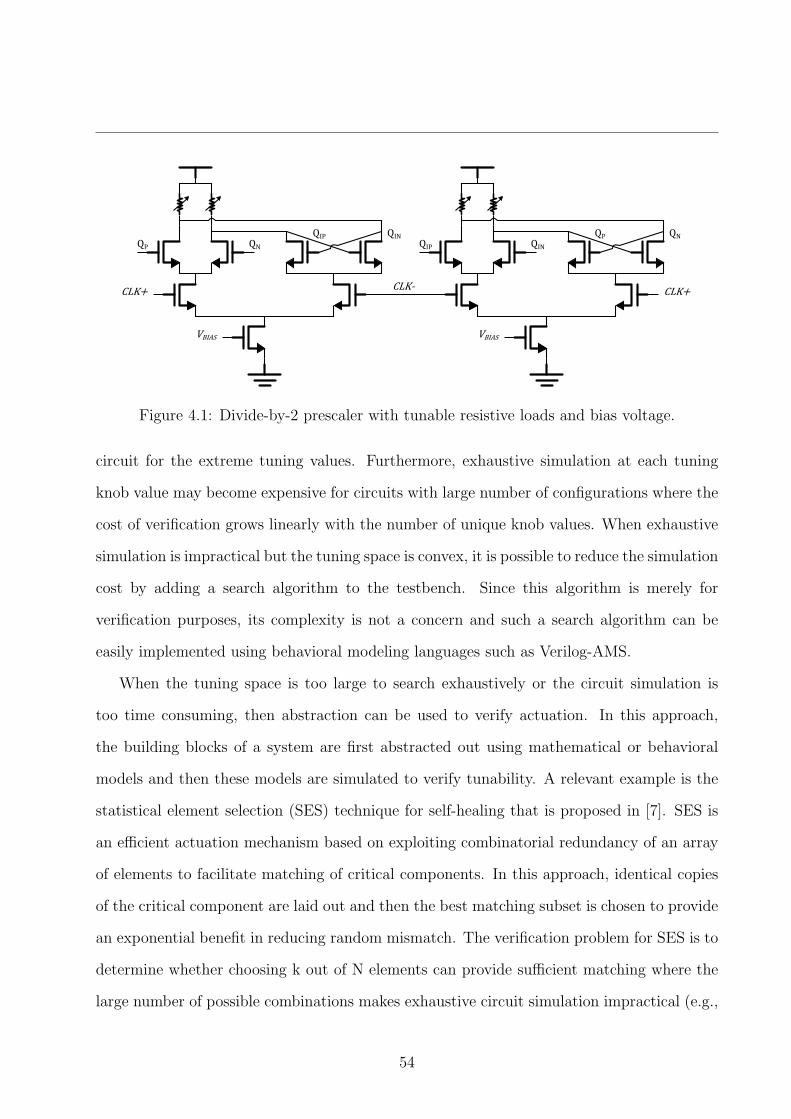
Figure 4.1: Divide-by-2 prescaler with tunable resistive loads and bias voltage.
circuit for the extreme tuning values. Furthermore, exhaustive simulation at each tuning
knob value may become expensive for circuits with large number of configurations where the
cost of verification grows linearly with the number of unique knob values. When exhaustive
simulation is impractical but the tuning space is convex, it is possible to reduce the simulation
cost by adding a search algorithm to the testbench. Since this algorithm is merely for
verification purposes, its complexity is not a concern and such a search algorithm can be
easily implemented using behavioral modeling languages such as Verilog-AMS.
When the tuning space is too large to search exhaustively or the circuit simulation is
too time consuming, then abstraction can be used to verify actuation. In this approach,
the building blocks of a system are first abstracted out using mathematical or behavioral
models and then these models are simulated to verify tunability. A relevant example is the
statistical element selection (SES) technique for self-healing that is proposed in [7]. SES is
an efficient actuation mechanism based on exploiting combinatorial redundancy of an array
of elements to facilitate matching of critical components. In this approach, identical copies
of the critical component are laid out and then the best matching subset is chosen to provide
an exponential benefit in reducing random mismatch. The verification problem for SES is to
determine whether choosing k out of N elements can provide sufficient matching where the
large number of possible combinations makes exhaustive circuit simulation impractical (e.g.,
54

there are 1820 combinations for k=4 and N=16). To solve this verification problem Keskin
first abstracts out an individual element by a random variable for which statistics can be
determined by circuit simulation easily. Then, the verification problem is solved by statistical
simulation of this random variable in Matlab. Another relevant example is the tunability
of PLL bandwidth and gain peaking where circuit simulation of PLL is prohibitive due to
stiffness. In this example, the verification problem is to determine whether the bandwidth
and peaking can be tuned to specifications using charge pump and loop filter tuning knobs.
Similar to the SES verification, this problem can be solved by abstracting the PLL building
blocks. First, the probability distribution or the range of block-level parameters can be
determined by circuit simulation of individual blocks. The tunability of bandwidth and
peaking can then be verified via a Monte Carlo simulation of the linear time invariant PLL
model given in (2.2) and using the parameter distributions and intervals.
4.3 Sensor
On-chip performance sensor is a key component of self-healing design. We would like
to verify the sensor accuracy since it determines the capabilities of self-healing. Small-scale
sensing circuits such as a peak detector or the temperature sensor can be verified by Monte
Carlo circuit simulation. The indirect phase noise sensor presented in Section 3.2.1 is also
verified by circuit simulation since the simulation time of VCO is manageable. However,
it is not practical to verify the indirect frequency response sensor presented in Section 3.3
by circuit simulation. This bandwidth sensor was demonstrated for continuous-time linear
time approximation of a dual-path charge-pump PLL, yet its accuracy has to be verified for
a more realistic PLL model that exhibits hybrid dynamics and nonlinearities. Since circuit
simulation is not practical for this verification problem, we employ nonlinear behavioral mod-
eling and simulation. For this purpose, we developed the behavioral model in Appendix .1
for PFD and CP and the behavioral model in Appendix .2 for VCO and DIV.
55
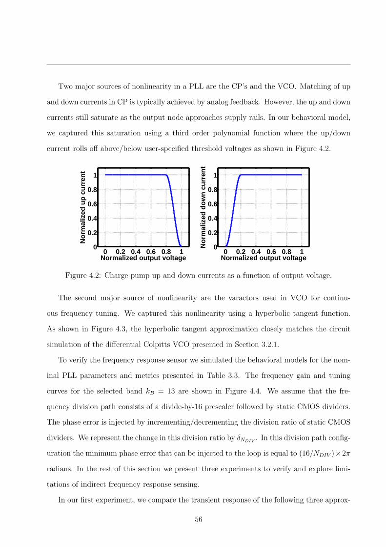
Two major sources of nonlinearity in a PLL are the CP’s and the VCO. Matching of up
and down currents in CP is typically achieved by analog feedback. However, the up and down
currents still saturate as the output node approaches supply rails. In our behavioral model,
we captured this saturation using a third order polynomial function where the up/down
current rolls off above/below user-specified threshold voltages as shown in Figure 4.2.
0 0.2 0.4 0.6 0.8 10
0.2
0.4
0.6
0.8
1
Nor
mal
ized
up
curr
ent
Normalized output voltage0 0.2 0.4 0.6 0.8 1
0
0.2
0.4
0.6
0.8
1
Nor
mal
ized
dow
n cu
rren
t
Normalized output voltage
Figure 4.2: Charge pump up and down currents as a function of output voltage.
The second major source of nonlinearity are the varactors used in VCO for continu-
ous frequency tuning. We captured this nonlinearity using a hyperbolic tangent function.
As shown in Figure 4.3, the hyperbolic tangent approximation closely matches the circuit
simulation of the differential Colpitts VCO presented in Section 3.2.1.
To verify the frequency response sensor we simulated the behavioral models for the nom-
inal PLL parameters and metrics presented in Table 3.3. The frequency gain and tuning
curves for the selected band kB = 13 are shown in Figure 4.4. We assume that the fre-
quency division path consists of a divide-by-16 prescaler followed by static CMOS dividers.
The phase error is injected by incrementing/decrementing the division ratio of static CMOS
dividers. We represent the change in this division ratio by δNDIV. In this division path config-
uration the minimum phase error that can be injected to the loop is equal to (16/NDIV )×2π
radians. In the rest of this section we present three experiments to verify and explore limi-
tations of indirect frequency response sensing.
In our first experiment, we compare the transient response of the following three approx-
56

0 0.2 0.4 0.6 0.8 10
0.2
0.4
0.6
0.8
1
Nor
mal
ized
freq
uenc
y
Normalized control voltage
Simulated responseHyperbolic tangent approximation
Figure 4.3: Comparison of hyperbolic tangent approximation of the varactor with circuitsimulation.
imations of the PLL:
• LTI refers to the continuous-time, linear time invariant approximation of the PLL
expressed in (2.3) and has been used in Section 3.2.1 to demonstrate indirect frequency
response sensing as a general method.
• Linear PLL refers to the discrete-time, linear time invariant approximation of the
PLL.
• Nonlinear PLL refers to the discrete-time, nonlinear time invariant approximation
of the PLL that is based on the behavioral models presented in Appendix .1 and
Appendix .2.
for varying δNDIV. Figure 4.5 shows the normalized phase error over time where the phase
error is injected at time zero. The response of linear PLL approximation closely tracks the
LTI response as expected when loop bandwidth is an order of magnitude smaller than the
reference frequency [9]. On the other hand, the response of the nonlinear PLL is slower and
underdamped where the deviation from linear response increases for increasing δNDIV.
In our second experiment we compare the transient response of nonlinear PLL for pos-
itive and negative change in static division ratio when the PLL is locked to 24.95GHz and
57

0 0.1 0.2 0.3 0.4 0.5 0.6 0.7 0.8 0.9 124.8
24.85
24.9
24.95
25
25.05
25.1
25.15
Fre
quen
cy (
GH
z)
Control voltage (V)
Integral pathProportional path
0 0.1 0.2 0.3 0.4 0.5 0.6 0.7 0.8 0.9 10
100
200
300
400
500
600
700
800
Fre
quen
cy g
ain
(MH
z/V
)
Control voltage (V)
Integral pathProportional path
Figure 4.4: Frequency tuning and gain curves for at band 13.
58

24.85GHz in band kB = 13. Figure 4.6 shows that the response for positive and negative
δNDIVcan be considerably different. This difference is due to the asymmetry in the frequency
gain around 24.85GHz (see Figure 4.4). Our last experiment shows that any static phase
offset in a PLL due to charge pump current mismatch or loop capacitor leakage may cause
incorrect crossover measurement. If the PLL suffers from a static phase offset, the indirect
bandwidth sensing circuitry will measure the time the input phase reaches this offset, as
shown in Figure 4.7, rather than the time the phase crosses zero. Although the average
of the crossover measurements for positive and negative phase error might provide a better
estimate on the first crossover, the timing of repetitive phase error injections will still be
impacted by static offset.
In summary, behavioral modeling and simulation provides a more accurate analysis of
PLL settling and revealed that indirect bandwidth and gain peaking sensing based on linear
models cannot be used for PLL’s with high nonlinearity and reduced supply headroom. More
specifically, crossover measurements can be corrupted significantly either by large change in
division ratio due to asymmetry and varactor nonlinearities or by small change in division
ratio due to static phase offsets.
59
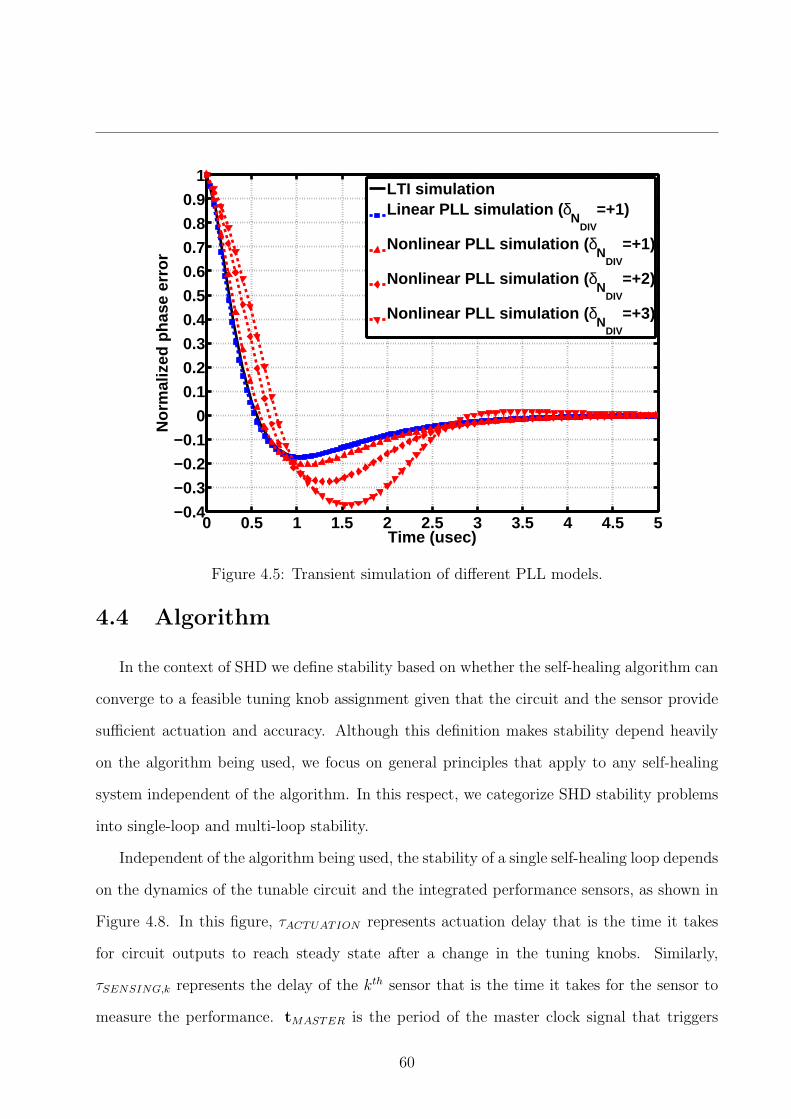
0 0.5 1 1.5 2 2.5 3 3.5 4 4.5 5−0.4
−0.3
−0.2
−0.1
0
0.1
0.2
0.3
0.4
0.5
0.6
0.7
0.8
0.9
1N
orm
aliz
ed p
hase
err
or
Time (usec)
LTI simulationLinear PLL simulation ( δ
NDIV
=+1)
Nonlinear PLL simulation ( δN
DIV
=+1)
Nonlinear PLL simulation ( δN
DIV
=+2)
Nonlinear PLL simulation ( δN
DIV
=+3)
Figure 4.5: Transient simulation of different PLL models.
4.4 Algorithm
In the context of SHD we define stability based on whether the self-healing algorithm can
converge to a feasible tuning knob assignment given that the circuit and the sensor provide
sufficient actuation and accuracy. Although this definition makes stability depend heavily
on the algorithm being used, we focus on general principles that apply to any self-healing
system independent of the algorithm. In this respect, we categorize SHD stability problems
into single-loop and multi-loop stability.
Independent of the algorithm being used, the stability of a single self-healing loop depends
on the dynamics of the tunable circuit and the integrated performance sensors, as shown in
Figure 4.8. In this figure, τACTUATION represents actuation delay that is the time it takes
for circuit outputs to reach steady state after a change in the tuning knobs. Similarly,
τSENSING,k represents the delay of the kth sensor that is the time it takes for the sensor to
measure the performance. tMASTER is the period of the master clock signal that triggers
60
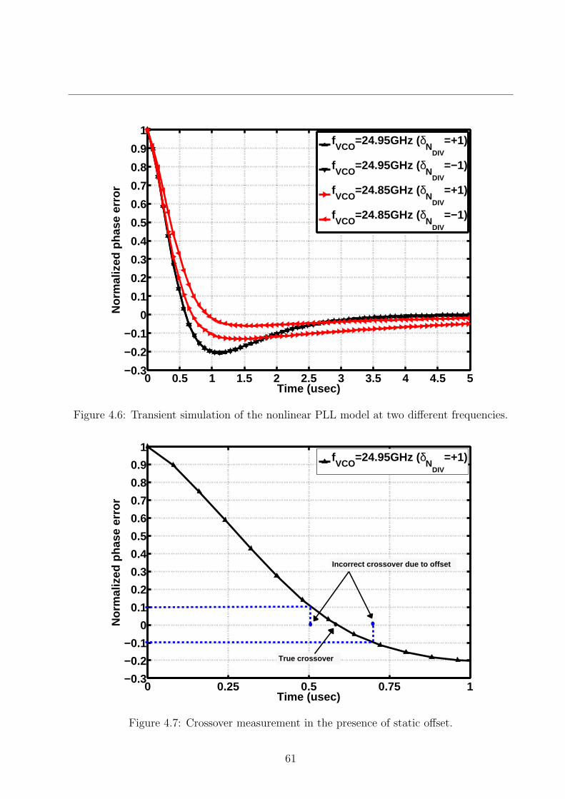
0 0.5 1 1.5 2 2.5 3 3.5 4 4.5 5−0.3
−0.2
−0.1
0
0.1
0.2
0.3
0.4
0.5
0.6
0.7
0.8
0.9
1N
orm
aliz
ed p
hase
err
or
Time (usec)
fVCO
=24.95GHz (δN
DIV
=+1)
fVCO
=24.95GHz (δN
DIV
=−1)
fVCO
=24.85GHz (δN
DIV
=+1)
fVCO
=24.85GHz (δN
DIV
=−1)
Figure 4.6: Transient simulation of the nonlinear PLL model at two different frequencies.
0 0.25 0.5 0.75 1−0.3
−0.2
−0.1
0
0.1
0.2
0.3
0.4
0.5
0.6
0.7
0.8
0.9
1
Nor
mal
ized
pha
se e
rror
Time (usec)
fVCO
=24.95GHz (δN
DIV
=+1)
True crossover
Incorrect crossover due to offset
Figure 4.7: Crossover measurement in the presence of static offset.
61
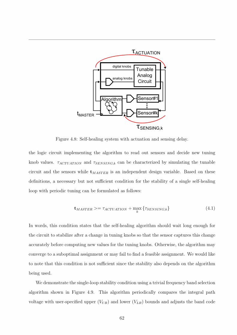
Tunable
Analog
Circuit
digital knobs
analog knobs
Algorithm Sensor#1
Sensor#ktMASTER
τACTUATION
τSENSING,k
Figure 4.8: Self-healing system with actuation and sensing delay.
the logic circuit implementing the algorithm to read out sensors and decide new tuning
knob values. τACTUATION and τSENSING,k can be characterized by simulating the tunable
circuit and the sensors while tMASTER is an independent design variable. Based on these
definitions, a necessary but not sufficient condition for the stability of a single self-healing
loop with periodic tuning can be formulated as follows:
tMASTER >= τACTUATION +maxkτSENSING,k (4.1)
In words, this condition states that the self-healing algorithm should wait long enough for
the circuit to stabilize after a change in tuning knobs so that the sensor captures this change
accurately before computing new values for the tuning knobs. Otherwise, the algorithm may
converge to a suboptimal assignment or may fail to find a feasible assignment. We would like
to note that this condition is not sufficient since the stability also depends on the algorithm
being used.
We demonstrate the single-loop stability condition using a trivial frequency band selection
algorithm shown in Figure 4.9. This algorithm periodically compares the integral path
voltage with user-specified upper (VUB) and lower (VLB) bounds and adjusts the band code
62
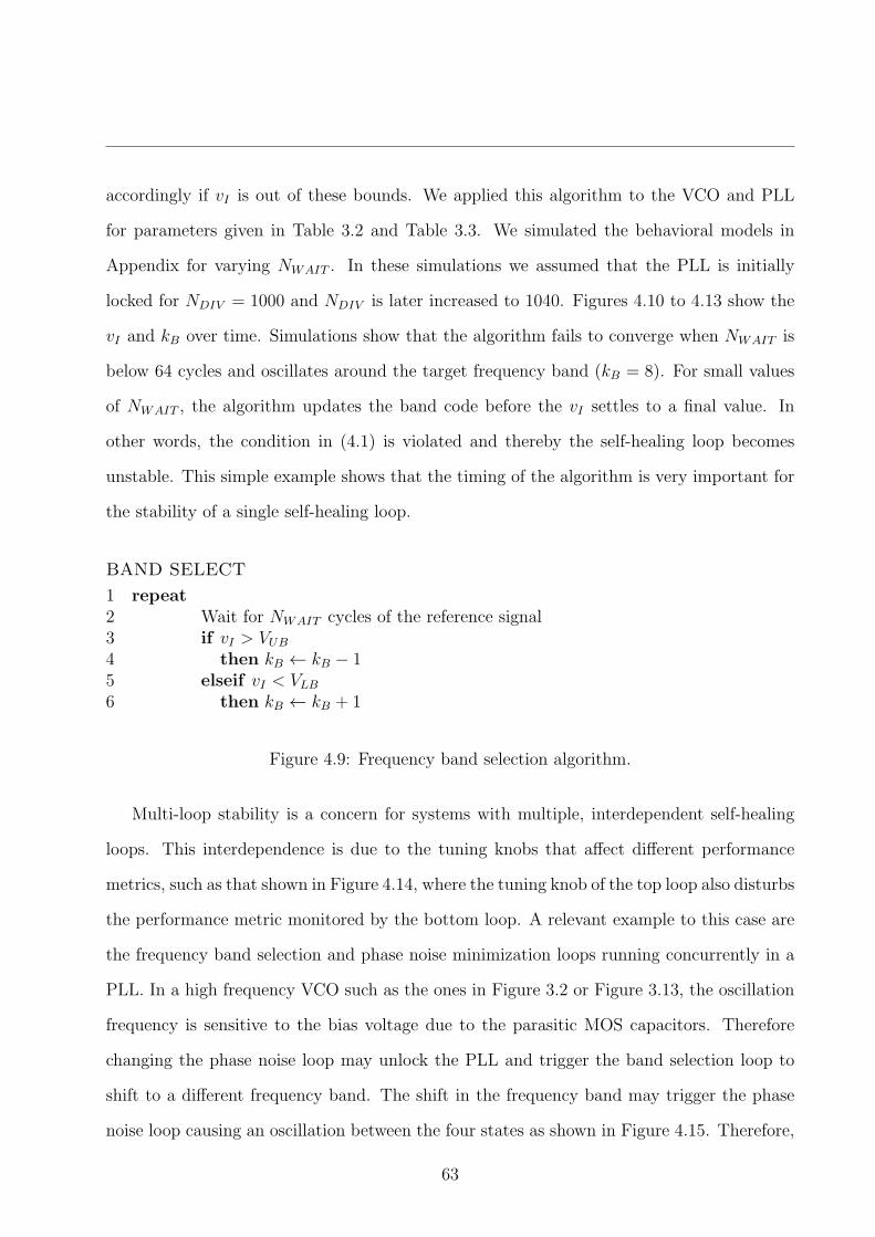
accordingly if vI is out of these bounds. We applied this algorithm to the VCO and PLL
for parameters given in Table 3.2 and Table 3.3. We simulated the behavioral models in
Appendix for varying NWAIT . In these simulations we assumed that the PLL is initially
locked for NDIV = 1000 and NDIV is later increased to 1040. Figures 4.10 to 4.13 show the
vI and kB over time. Simulations show that the algorithm fails to converge when NWAIT is
below 64 cycles and oscillates around the target frequency band (kB = 8). For small values
of NWAIT , the algorithm updates the band code before the vI settles to a final value. In
other words, the condition in (4.1) is violated and thereby the self-healing loop becomes
unstable. This simple example shows that the timing of the algorithm is very important for
the stability of a single self-healing loop.
BAND SELECT
1 repeat
2 Wait for NWAIT cycles of the reference signal3 if vI > VUB
4 then kB ← kB − 15 elseif vI < VLB
6 then kB ← kB + 1
Figure 4.9: Frequency band selection algorithm.
Multi-loop stability is a concern for systems with multiple, interdependent self-healing
loops. This interdependence is due to the tuning knobs that affect different performance
metrics, such as that shown in Figure 4.14, where the tuning knob of the top loop also disturbs
the performance metric monitored by the bottom loop. A relevant example to this case are
the frequency band selection and phase noise minimization loops running concurrently in a
PLL. In a high frequency VCO such as the ones in Figure 3.2 or Figure 3.13, the oscillation
frequency is sensitive to the bias voltage due to the parasitic MOS capacitors. Therefore
changing the phase noise loop may unlock the PLL and trigger the band selection loop to
shift to a different frequency band. The shift in the frequency band may trigger the phase
noise loop causing an oscillation between the four states as shown in Figure 4.15. Therefore,
63
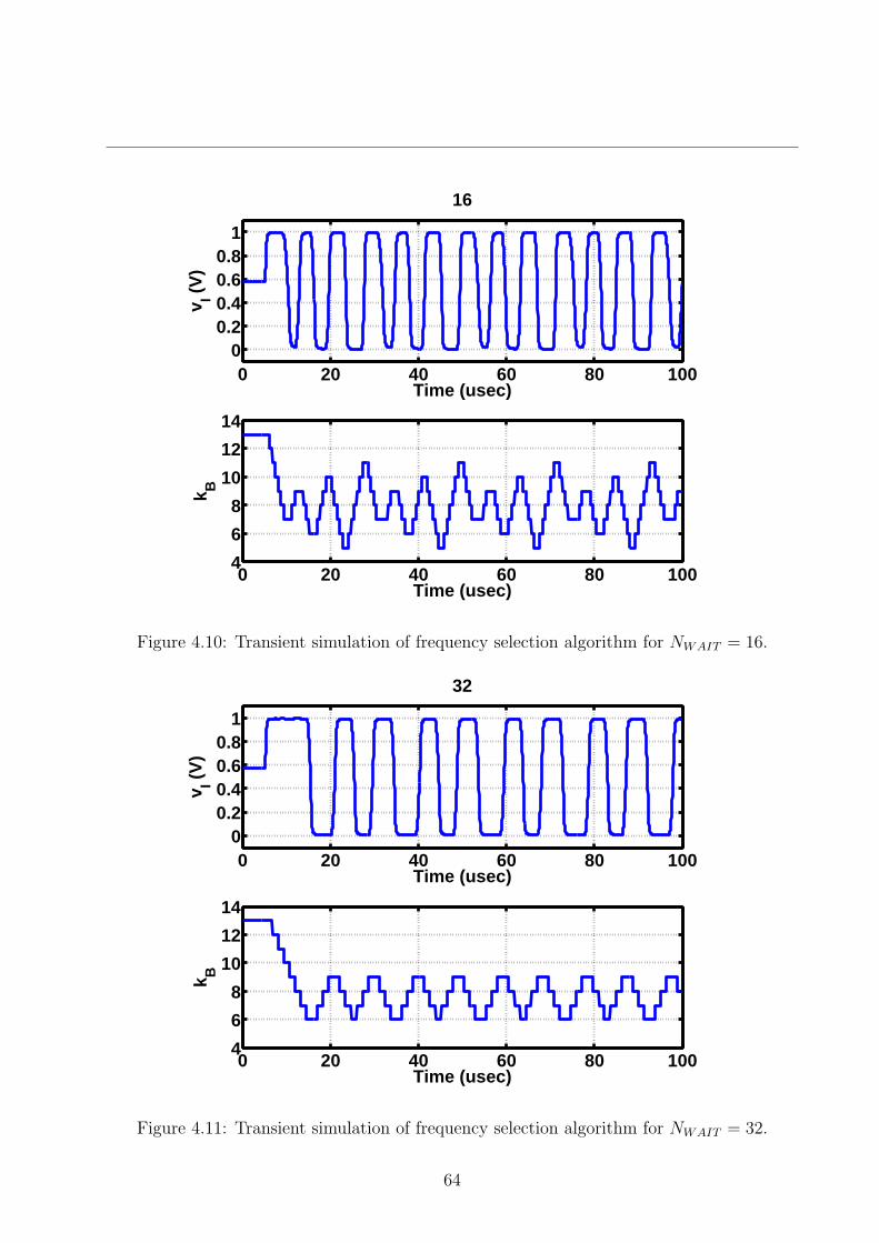
0 20 40 60 80 1000
0.20.40.60.8
1
v I (V
)
Time (usec)
16
0 20 40 60 80 1004
6
8
10
12
14
k B
Time (usec)
Figure 4.10: Transient simulation of frequency selection algorithm for NWAIT = 16.
0 20 40 60 80 1000
0.20.40.60.8
1
v I (V
)
Time (usec)
32
0 20 40 60 80 1004
6
8
10
12
14
k B
Time (usec)
Figure 4.11: Transient simulation of frequency selection algorithm for NWAIT = 32.
64
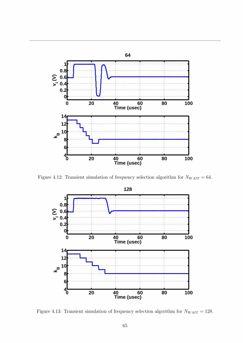
0 20 40 60 80 1000
0.20.40.60.8
1
v I (V
)
Time (usec)
64
0 20 40 60 80 1004
6
8
10
12
14
k B
Time (usec)
Figure 4.12: Transient simulation of frequency selection algorithm for NWAIT = 64.
0 20 40 60 80 1000
0.20.40.60.8
1
v I (V
)
Time (usec)
128
0 20 40 60 80 1004
6
8
10
12
14
k B
Time (usec)
Figure 4.13: Transient simulation of frequency selection algorithm for NWAIT = 128.
65
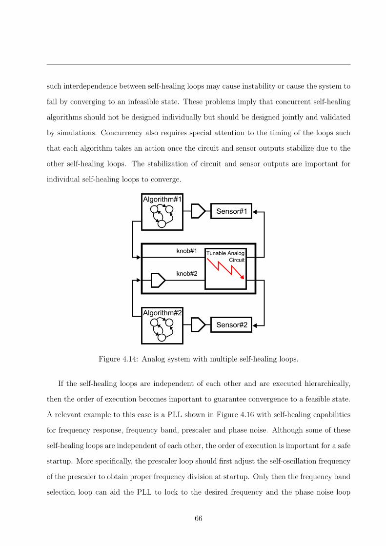
such interdependence between self-healing loops may cause instability or cause the system to
fail by converging to an infeasible state. These problems imply that concurrent self-healing
algorithms should not be designed individually but should be designed jointly and validated
by simulations. Concurrency also requires special attention to the timing of the loops such
that each algorithm takes an action once the circuit and sensor outputs stabilize due to the
other self-healing loops. The stabilization of circuit and sensor outputs are important for
individual self-healing loops to converge.
Algorithm#2
Sensor#2
Algorithm#1
Sensor#1
knob#1
knob#2
Tunable Analog
Circuit
Figure 4.14: Analog system with multiple self-healing loops.
If the self-healing loops are independent of each other and are executed hierarchically,
then the order of execution becomes important to guarantee convergence to a feasible state.
A relevant example to this case is a PLL shown in Figure 4.16 with self-healing capabilities
for frequency response, frequency band, prescaler and phase noise. Although some of these
self-healing loops are independent of each other, the order of execution is important for a safe
startup. More specifically, the prescaler loop should first adjust the self-oscillation frequency
of the prescaler to obtain proper frequency division at startup. Only then the frequency band
selection loop can aid the PLL to lock to the desired frequency and the phase noise loop
66
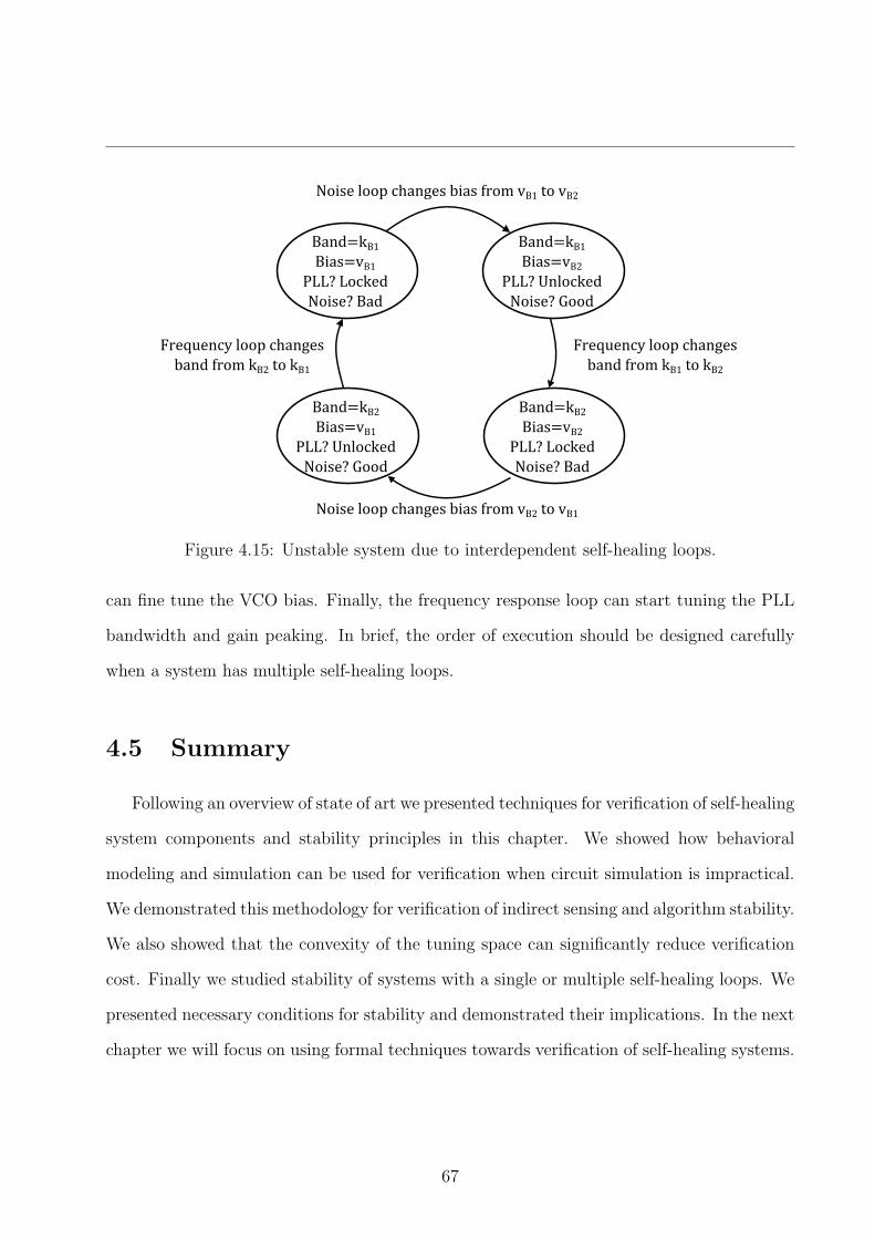
Band=kB1Bias=vB1
PLL?Locked
Noise?Bad
Band=kB1Bias=vB2
PLL?Unlocked
Noise?Good
NoiseloopchangesbiasfromvB1tovB2
Band=kB2Bias=vB1
PLL?Unlocked
Noise?Good
Band=kB2Bias=vB2
PLL?Locked
Noise?Bad
Frequencyloopchanges
bandfromkB1tokB2
NoiseloopchangesbiasfromvB2tovB1
Frequencyloopchanges
bandfromkB2tokB1
Figure 4.15: Unstable system due to interdependent self-healing loops.
can fine tune the VCO bias. Finally, the frequency response loop can start tuning the PLL
bandwidth and gain peaking. In brief, the order of execution should be designed carefully
when a system has multiple self-healing loops.
4.5 Summary
Following an overview of state of art we presented techniques for verification of self-healing
system components and stability principles in this chapter. We showed how behavioral
modeling and simulation can be used for verification when circuit simulation is impractical.
We demonstrated this methodology for verification of indirect sensing and algorithm stability.
We also showed that the convexity of the tuning space can significantly reduce verification
cost. Finally we studied stability of systems with a single or multiple self-healing loops. We
presented necessary conditions for stability and demonstrated their implications. In the next
chapter we will focus on using formal techniques towards verification of self-healing systems.
67
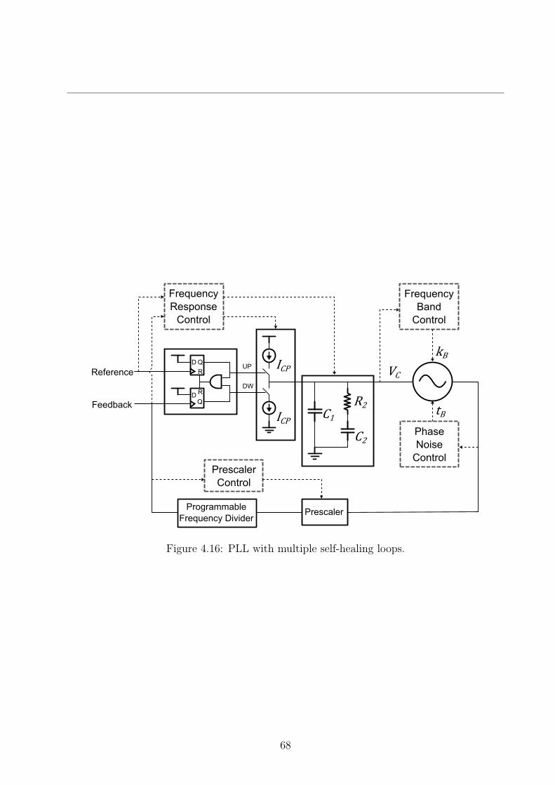
Figure 4.16: PLL with multiple self-healing loops.
68

Chapter 5
Towards Formal Verification of
Self-Healing Systems
In the previous chapter we identified major challenges in verification of self-healing sys-
tems and presented general methodologies to address these challenges. In this chapter we
explore formal techniques to verify self-healing systems in collaboration with Matthias Al-
thoff and Akshay Rajhans. Formal methods verify the performance of a circuit over entire
ranges of parameter variations and initial conditions without using exhaustive simulation.
We begin with a detailed overview of state-of-art formal verification for analog circuits in
Section 5.1. In Section 5.2 we present a hybrid PLL model that enables reachability analysis.
In Section 5.3 we discuss the applicability and limits of reachability analysis for self-healing
circuits.
5.1 Overview of Formal Analog Verification
Formal verification refers to techniques that can mathematically prove a set of properties
about a system. Formal techniques in general are categorized into theorem proving and
state space exploration. Theorem proving refers to establishing mathematical proofs using
a set of axioms and inference rules. State space exploration, which is more relevant to
69
analog circuits, is based on exploring all or a subset of states that a system can reach.
Two key problems in state space exploration are equivalence checking and model checking.
Equivalence checking refers to verification of functional similarity between two systems or
two different representations of the same system. Model checking refers to verification of
whether a system does conform with a given set of properties. This is achieved via reachability
analysis, which determines the set of reachable states of a system starting from an initial set
of states for given inputs and parameter uncertainties.
Equivalence and model checking have been successfully applied to digital integrated cir-
cuits [32]. This has been possible primarily due to the fact that the state space of digital
circuits is discrete and finite. Furthermore, digital circuits can be abstracted by Boolean
functions and allow a canonical representation such as binary decision diagrams. The equiv-
alence and model checking can be formulated as Boolean satisfiability problems where effi-
cient solvers are already available. The efficacy of formal verification techniques, however,
is limited by the size of the state space. The computational time and memory requirements
typically depend exponentially on the size of the state space (a.k.a. the state space explosion
problem).
The success of formal techniques for digital circuits have resulted in a growing interest
in developing formal verification techniques for analog circuits. Model checking can help
analog design to verify performance over a given range of process variations, environment
variations or circuit inputs. Equivalence checking can help to verify whether the circuit and
its behavioral model are functionally similar for any possible input. In the rest of this section
we provide an overview of previous research on formal verification of analog circuits. A more
detailed survey can be found in [33].
In [34], Hedrich et. al addressed the equivalence checking of nonlinear analog circuits and
proposed a technique to compare nonlinear state space representations of two systems. In
this method, the nonlinear systems are linearized at a selected set of points in the state space
and a linear state transformation map from one system to the other is derived heuristically.
70
Using this map, the vector and scalar fields at the selected points are compared to check the
equivalence of the two systems.
Equivalence checking of linear or linearized analog circuits (e.g., filters and operational
amplifiers) with a specification in the form of a linear transfer function is addressed in
[35, 36, 37]. These techniques begin with a symbolic transfer function of the analog circuit
in s-domain. In [35], the s-domain transfer function of the system and specification are
transformed into z-domain using bilinear transformation. The discretized transfer functions
are then realized using adders, multipliers and delay elements resulting in a finite state
machine. Authors adopted digital verification techniques to check the equivalence of these
finite state machine abstractions. In [36], the value sets of the transfer functions of the
system and the specification are computed over given frequency and coefficient intervals
on the complex plane. The equivalence is established by checking whether the value set
of the system is a subset of the value set of the specification. In [37], the magnitude and
phase response of the transfer function of the circuit and the specification are compared over
frequency intervals in a nonlinear optimization framework.
Model checking techniques for analog circuits can be categorized into discretization-based
methods and reachability analysis. The first set of methods discretize the continuous state
space of analog circuits, namely the node voltages and branch currents, and discretize the
continuous time into time steps [38, 39, 40]. This discretization results in a finite state
abstraction of the analog circuit where the transition relations are either determined from
simulations or numerical techniques such as interval arithmetic. Then, the finite state ab-
straction is verified by using model checking tools developed for digital circuits. These
techniques have been applied to small-scale circuits since the discretization in space and
time cause state explosion.
The second set of model checking methods employ the reachability analysis techniques
developed for continuous or hybrid systems [41, 42]. A hybrid system (a.k.a. hybrid automa-
ton) is represented by a directed graph and consists of a set of discrete modes and continuous
71
dynamics in each mode [43]. Each vertex is associated with a set of differential equations
modeling continuous dynamics while each edge is associated with a jump condition and a
relation that models discrete events and modifications to the continuous variables. Although
hybrid automaton can be used to model a wide variety of systems, the reachable states can
be computed exactly only for very simple cases where continuous dynamics can be expressed
by intervals on the derivatives of continuous variables [44]. Therefore, various approxima-
tions are used to compute reachable states for linear or nonlinear continuous dynamics. More
details and recent progress on reachability analysis can be found in [44, 45]. Reachability
analysis have been applied to very small-scale circuits including interlock circuits and simple
oscillators [33]. In the following section, we present how reachability analysis can be applied
to verify the stability of a dual-path, charge-pump PLL.
5.2 Reachability Analysis for PLL
A key performance specification for PLL’s is the locking time, which is the time it takes
to achieve phase and frequency locking after a change in division ratio or after a perturba-
tion to the system. Although linear time invariant approximations of PLL’s are useful for
checking stability [9], locking time analysis requires transient simulations due to the hybrid
nature of the system. Since a single circuit simulation can take weeks for high frequency
PLL’s, behavioral modeling and simulation is widely used to determine the locking time.
Although behavioral simulation offers a significant speed up, it cannot guarantee locking for
all possible initial conditions and parameters variations. Due to the continuous variables in
PLL dynamics, a finite set of simulations is not sufficient to determine the worst-case lock-
ing time. Consequently there is still a need for formal verification of the PLL locking time.
In this section we explore whether reachability analysis can be applied for this problem in
collaboration with Matthias Althoff and Akshay Rajhans. We first present a hybrid model
for a dual-path, charge-pump PLL. We then summarize how reachability analysis can be
72
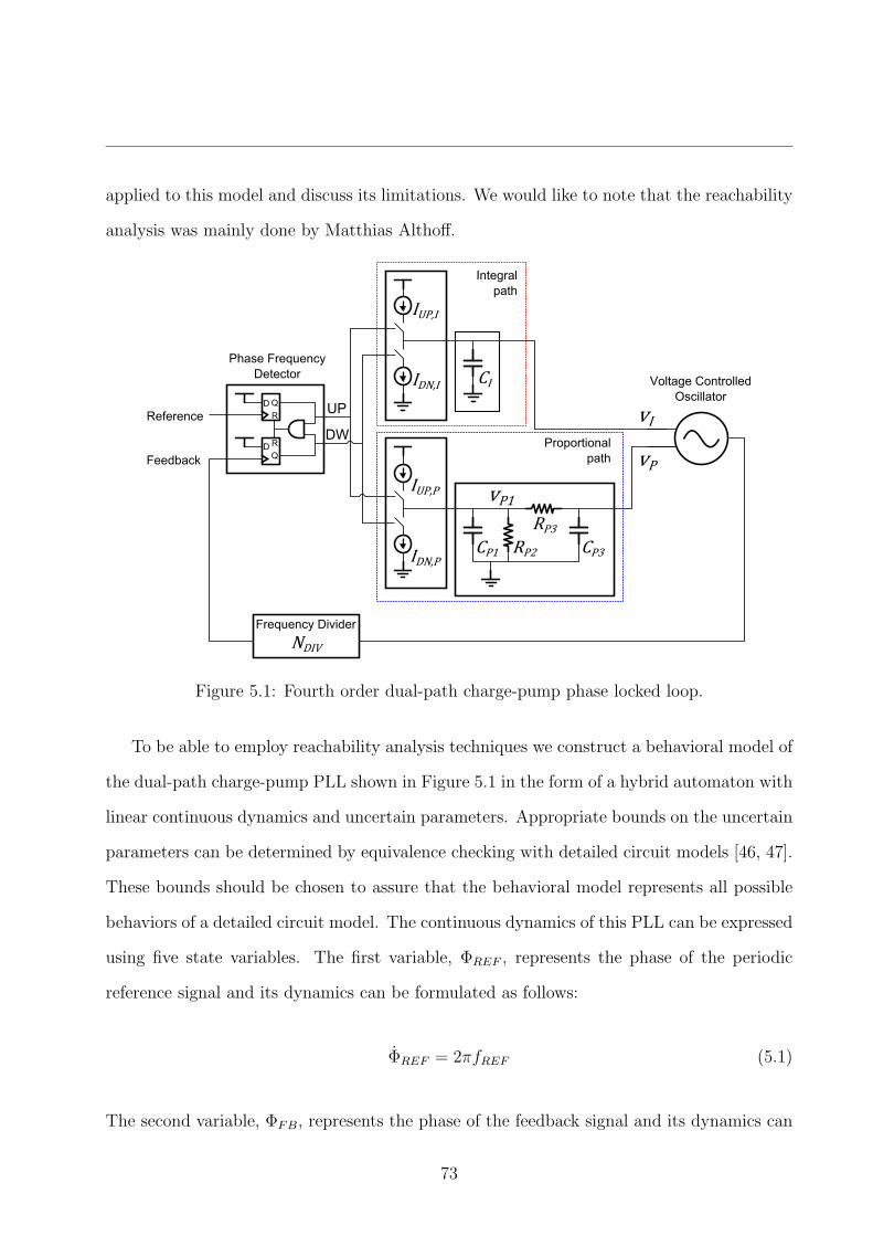
applied to this model and discuss its limitations. We would like to note that the reachability
analysis was mainly done by Matthias Althoff.
Figure 5.1: Fourth order dual-path charge-pump phase locked loop.
To be able to employ reachability analysis techniques we construct a behavioral model of
the dual-path charge-pump PLL shown in Figure 5.1 in the form of a hybrid automaton with
linear continuous dynamics and uncertain parameters. Appropriate bounds on the uncertain
parameters can be determined by equivalence checking with detailed circuit models [46, 47].
These bounds should be chosen to assure that the behavioral model represents all possible
behaviors of a detailed circuit model. The continuous dynamics of this PLL can be expressed
using five state variables. The first variable, ΦREF , represents the phase of the periodic
reference signal and its dynamics can be formulated as follows:
ΦREF = 2πfREF (5.1)
The second variable, ΦFB, represents the phase of the feedback signal and its dynamics can
73

be formulated as follows:
ΦFB =2π
NDIV
(f0 +KPvP +KIvI) (5.2)
where f0 is the center frequency of the VCO, KP and KI are the proportional and integral
path frequency gains, vP and vI are the proportional and integral path voltages. The dif-
ferential equations for vI and vP and vP1 can be expressed by writing and arranging KCL
equations at the corresponding nodes as
vI =1
CI
(IUP,I − IDN,I) (5.3)
vP =1
CP3RP3
vP1 −1
CP3RP3
vP (5.4)
˙vP1 =1
CP1
(IUP,P − IDN,P ) +1
CP1RP3
vP −1
CP1
(
1
RP2
+1
RP3
)
vP1 (5.5)
If we present the five state variables with a vector x = [vI , vP1, vP ,ΦFB,ΦREF ]T , the dynamics
can be represented in a matrix form as
x = Ax+ Bu+ c (5.6)
where
A =
0 0 0 0 0
0 − 1CP1
(
1RP2
+ 1RP3
)
1CP1RP3
0 0
0 1CP3RP3
− 1CP3RP3
0 0
2πKI
NDIV
0 2πKP
NDIV
0 0
0 0 0 0 0
,
74
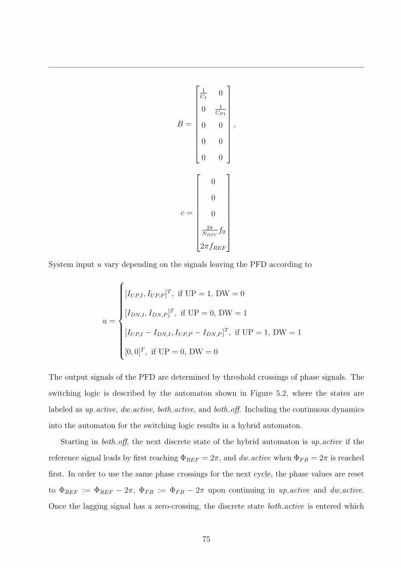
B =
1CI
0
0 1CP1
0 0
0 0
0 0
,
c =
0
0
0
2πNDIV
f0
2πfREF
System input u vary depending on the signals leaving the PFD according to
u =
[IUP,I , IUP,P ]T , if UP = 1, DW = 0
[IDN,I , IDN,P ]T , if UP = 0, DW = 1
[IUP,I − IDN,I , IUP,P − IDN,P ]T , if UP = 1, DW = 1
[0, 0]T , if UP = 0, DW = 0
The output signals of the PFD are determined by threshold crossings of phase signals. The
switching logic is described by the automaton shown in Figure 5.2, where the states are
labeled as up active, dw active, both active, and both off. Including the continuous dynamics
into the automaton for the switching logic results in a hybrid automaton.
Starting in both off, the next discrete state of the hybrid automaton is up active if the
reference signal leads by first reaching ΦREF = 2π, and dw active when ΦFB = 2π is reached
first. In order to use the same phase crossings for the next cycle, the phase values are reset
to ΦREF := ΦREF − 2π, ΦFB := ΦFB − 2π upon continuing in up active and dw active.
Once the lagging signal has a zero-crossing, the discrete state both active is entered which
75
both_active
UP=1,DW=1
up_active
UP=1,DW=0
dw_active
UP=0,DW=1
both_off
UP=0,DW=0
guard:t==td
guard:ΦFB==0
reset:t:=0
guard:ΦFB==0
reset:ΦFB:=0
ΦREF:=ΦREF-2π
guard:ΦREF==0
reset:ΦREF:=0
ΦFB:=ΦFB-2π
guard:ΦREF==0
reset:t:=0
Figure 5.2: Hybrid automaton for phase frequency detector.
models a time delay td for switching off both charge pumps. After the delay, the system is
in both off again, which completes one cycle. Locking is achieved when the phase difference
reaches and remains within the locked condition given by the interval [−0.1, 0.1]. There
are two specifications that need to be verified:
• Given the PLL starting from any initial state and any valid set of parameters, verify
that the locked condition is reached in less than k cycles.
• Given a set of states reached from any initial state and any valid set of parameters
such that all states are in the locked condition, show that starting from any state in
the given set the PLL state remains in the locked condition indefinitely.
Although simulations may show that the PLL remains in the locked condition for many
cycles after k, finite-length simulations can never guarantee the locked condition to hold
indefinitely. To the best of our knowledge, none of the existing methods in the literature has
been used to verify PLL lock time because of the extremely long transient time required for
convergence. Attempts to apply brute force hybrid system reachability using tools such as
PHAVer [48] or SpaceEx [49] failed due to the slow convergence close to locking.
In [50] we demonstrated that this behavioral model of the charge-pump PLL can be
formally verified in time comparable to the time required for Monte Carlo simulations of the
same model. In contrast to other hybrid systems that have been analyzed in the literature,
76
PLL’s require thousands of switchings in the continuous dynamics to converge sufficiently
close to a limit cycle. This makes reachability analysis a challenging task since switchings in
the dynamics are expensive to compute and result in conservative overapproximations. We
attacked this challenge by continuization of the switching dynamics: a continuous model is
derived that replaces the switching conditions with uncertain parameters. Using reachability
analysis for linear systems with uncertain parameters, all states reachable by any possible
simulation of the original model can be computed using the continuous model. We also
showed that the added uncertainty does not result in a large overapproximation of cycles for
which locking of the PLL can be verified. Overapproximation might lead to the conclusion
that the PLL does not lock, although in reality it does. If the overapproximations are tight,
a negative result still implies the circuit design is not sufficiently robust against parameter
uncertainty.
Using this continuization technique we successfully verified the locking time of a 25GHz
PLL design with up to 10 percent relative variation in charge pump currents and 10 percent
variation in initial phase difference. The considered PLL employs a simple initialization
circuitry that sets the integral and proportional path voltages to common-mode levels at
power up and whenever the division ratio is changed. This initialization circuitry reduces
locking time and aids the formal verification by reducing the uncertainty on the initial
node voltages. Figure 5.3 shows the reachable set projected onto four different pairs of
state variables for the first 200 cycles. The reachable set at each cycle (represented by
rectangles) accurately encapsulate the individual simulation runs (represented by dots). The
computational time of the proposed technique is shown to be comparable to a simulation
of the same behavioral model in Matlab. Although simulating the behavioral PLL model
in Verilog-AMS for a particular initial condition found to be an order of magnitude faster
than reachability analysis, reachability analysis is still competitive since the Verilog-AMS
model needs to be simulated for thousands of Monte Carlo samples to capture random
initial conditions and parameter variations.
77
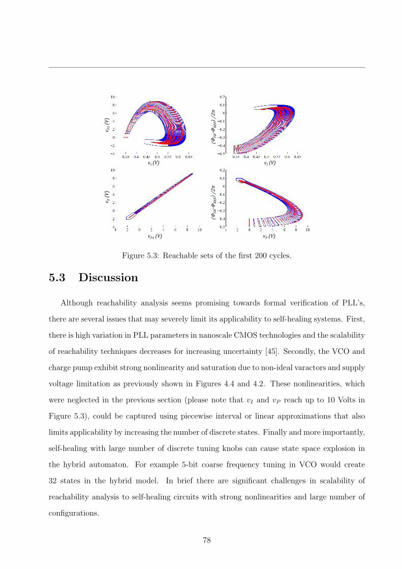
vI (V) vI (V)
vP1 (V) vP (V)
(ΦFB-Φ
REF)/2π
(ΦFB-Φ
REF)/2π
vP(V)
vP1(V)
Figure 5.3: Reachable sets of the first 200 cycles.
5.3 Discussion
Although reachability analysis seems promising towards formal verification of PLL’s,
there are several issues that may severely limit its applicability to self-healing systems. First,
there is high variation in PLL parameters in nanoscale CMOS technologies and the scalability
of reachability techniques decreases for increasing uncertainty [45]. Secondly, the VCO and
charge pump exhibit strong nonlinearity and saturation due to non-ideal varactors and supply
voltage limitation as previously shown in Figures 4.4 and 4.2. These nonlinearities, which
were neglected in the previous section (please note that vI and vP reach up to 10 Volts in
Figure 5.3), could be captured using piecewise interval or linear approximations that also
limits applicability by increasing the number of discrete states. Finally and more importantly,
self-healing with large number of discrete tuning knobs can cause state space explosion in
the hybrid automaton. For example 5-bit coarse frequency tuning in VCO would create
32 states in the hybrid model. In brief there are significant challenges in scalability of
reachability analysis to self-healing circuits with strong nonlinearities and large number of
configurations.
78

Chapter 6
Conclusion
In this dissertation, we studied design methodologies for self-healing systems that can
autonomously restore performance loss due to process and environment variability via on-
chip sensing and control circuitry. Self-healing, which trades off different performance metrics
to meet design specifications, can also optimize the circuits with multiple operating modes
where the performance is sensitive to the circuit state. We focused on self-healing via digital
tuning that refers to selection of a subset of devices and/or discrete biasing levels. Digital
tuning is widely applicable, can be guaranteed to be stable and enables actuation in newer
process technologies with decreasing voltage headroom unlike continuous analog feedback.
We addressed what we consider to be the major challenges in designing self-healing systems
with digital tuning: integrated performance sensing; robust algorithm design and verification
before manufacturing.
We proposed the use of indirect sensing for performance metrics that are not easily mea-
sured on-chip either due to high integration overhead or physical limitations. Indirect per-
formance sensor predicts the performance of interest as a function of other easy-to-measure
performance metrics, already-known circuit inputs and tuning knobs by exploiting the cor-
relations in between. Indirect sensing assumes that the simulation of device models should
capture the correlation between performance metrics and the sensitivity of performance
79
metrics to tuning knobs. However, the absolute accuracy of simulated performance is not
critical since any systematic offset between the simulated and measured performance can
be determined and compensated during post-manufacturing tests. We presented a design
methodology for indirect performance sensors that minimizes the on-chip integration over-
head.
We then studied the challenges in the verification of self-healing system components:
actuation, sensor and algorithm with relevant circuit examples. Self-healing design makes
verification more difficult compared to conventional design by increasing circuit complexity
and by bringing new issues to consider. We demonstrated how behavioral modeling and
simulation can be used for verification when circuit simulation is impractical. We showed
that the convexity of the tuning space can significantly simplify algorithm design and reduce
verification cost. We presented necessary conditions on the stability of systems with a single
and multiple self-healing loops. We also explored applicability of formal techniques towards
verification of self-healing systems.
We demonstrated our work using a challenging design example, phase locked loop (PLL)
that requires multiple self-healing loops to push the performance envelope. We first demon-
strated indirect phase noise sensing for two different voltage controlled oscillator circuits
using simulated and measured results. We showed self-healing using indirect phase noise
sensing can improve the parametric yield and reduce power dissipation. Secondly, we demon-
strated indirect bandwidth and gain peaking sensors for PLL’s. We extended an existing
all-digital bandwidth sensor by a new technique which significantly improves sensor accuracy.
We finally presented a hybrid PLL model that enables reachability analysis and discussed
the generalization of reachability analysis to self-healing circuits.
This thesis can be extended and generalized in the following directions:
• To create a manageable scope of work we only focused on self-healing phase locked loops
in this thesis. Efficient actuation and sensing solutions can be explored for high-speed
serial input output and RF front end circuits.
80

• The self-healing examples considered in this thesis had very few tuning knobs and
design specifications. Consequently, simple search algorithms were sufficient for self-
healing. Efficient algorithm design can be studied for systems with many tuning knobs
and multiple performance metrics.
• Formal methods are very powerful since they verify the performance of a circuit over
entire ranges of parameter variations and initial conditions without using exhaustive
simulation. However, large-scale parameter variations, device nonlinearities and dig-
ital tuning can significantly limit the applicability of formal methods for self-healing
systems. Due to these challenges, further research on formal techniques can focus more
on verifying the interface between analog and digital circuits or the digital components
of self-healing systems rather than performance verification of nonlinear and complex
analog circuits.
81
Bibliography
[1] B. Razavi, Design of Analog CMOS Integrated Circuits, 1st ed. New York, NY, USA:
McGraw-Hill, Inc., 2001.
[2] J. Maneatis, “Low-jitter and process independent dll and pll based on self biased tech-
niques,” in Solid-State Circuits Conference, 1996. Digest of Technical Papers. 42nd
ISSCC., 1996 IEEE International, feb 1996, pp. 130 –131, 430.
[3] M. Margarit, J. L. Tham, R. Meyer, and M. Deen, “A low-noise, low-power vco with au-
tomatic amplitude control for wireless applications,” Solid-State Circuits, IEEE Journal
of, vol. 34, no. 6, pp. 761 –771, jun 1999.
[4] G. Keskin, J. Proesel, and L. Pileggi, “Statistical modeling and post manufacturing con-
figuration for scaled analog cmos,” in Custom Integrated Circuits Conference (CICC),
2010 IEEE, sept. 2010, pp. 1–4.
[5] V. Natarajan, S. Sen, A. Banerjee, A. Chatterjee, G. Srinivasan, and F. Taenzler,
“Analog signature- driven postmanufacture multidimensional tuning of rf systems,”
Design Test of Computers, IEEE, vol. 27, no. 6, pp. 6 –17, nov.-dec. 2010.
[6] N. Kupp, H. Huang, Y. Makris, and P. Drineas, “Improving analog and rf device yield
through performance calibration,” Design Test of Computers, IEEE, vol. 28, no. 3, pp.
64 –75, may-june 2011.
82
[7] G. Keskin, “Self-healing circuits using statistical element selection,” Dissertation,
Carnegie Mellon University, 2010.
[8] J. Craninckx and M. Steyaert, “A fully integrated cmos dcs-1800 frequency synthesizer,”
Solid-State Circuits, IEEE Journal of, vol. 33, no. 12, pp. 2054 –2065, dec 1998.
[9] F. M. Gardner, Phaselock Techniques, 3rd ed. Hoboken, NJ, USA: John Wiley, 2005.
[10] A. Kral, F. Behbahani, and A. Abidi, “Rf-cmos oscillators with switched tuning,” in
Custom Integrated Circuits Conference, 1998. Proceedings of the IEEE 1998, may 1998,
pp. 555 –558.
[11] A. Berny, A. Niknejad, and R. Meyer, “A 1.8-ghz lc vco with 1.3-ghz tuning range and
digital amplitude calibration,” Solid-State Circuits, IEEE Journal of, vol. 40, no. 4, pp.
909 – 917, april 2005.
[12] T.-H. Lin and Y.-J. Lai, “An agile vco frequency calibration technique for a 10-ghz cmos
pll,” Solid-State Circuits, IEEE Journal of, vol. 42, no. 2, pp. 340 –349, feb. 2007.
[13] J. Shin and H. Shin, “A fast and high-precision vco frequency calibration technique
for wideband δσ fractional-n frequency synthesizers,” Circuits and Systems I: Regular
Papers, IEEE Transactions on, vol. 57, no. 7, pp. 1573 –1582, july 2010.
[14] J. Rogers, D. Rahn, and C. Plett, “A study of digital and analog automatic-amplitude
control circuitry for voltage-controlled oscillators,” Solid-State Circuits, IEEE Journal
of, vol. 38, no. 2, pp. 352 – 356, feb 2003.
[15] A. Maxim, “A multi-rate 9.953-12.5-ghz 0.2-µm sige bicmos lc oscillator using a resistor-
tuned varactor and a supply pushing cancellation circuit,” Solid-State Circuits, IEEE
Journal of, vol. 41, no. 4, pp. 918 –934, april 2006.
83
[16] W. Khalil, B. Bakkaloglu, and S. Kiaei, “A self-calibrated on-chip phase-noise measure-
ment circuit with -75 dbc single-tone sensitivity at 100 khz offset,” Solid-State Circuits,
IEEE Journal of, vol. 42, no. 12, pp. 2758 –2765, dec. 2007.
[17] K. Jenkins, K. Shepard, and Z. Xu, “On-chip circuit for measuring period jitter and
skew of clock distribution networks,” in Custom Integrated Circuits Conference, 2007.
CICC ’07. IEEE, sept. 2007, pp. 157 –160.
[18] J. Kim, “Adaptive-bandwidth phase-locked loop with continuous background frequency
calibration,” Circuits and Systems II: Express Briefs, IEEE Transactions on, vol. 56,
no. 3, pp. 205 –209, march 2009.
[19] T. Wu, P. Hanumolu, K. Mayaram, and U.-K. Moon, “Method for a constant loop
bandwidth in lc-vco pll frequency synthesizers,” Solid-State Circuits, IEEE Journal of,
vol. 44, no. 2, pp. 427 –435, feb. 2009.
[20] D. Fischette, A. Loke, R. DeSantis, and G. Talbot, “An embedded all-digital circuit to
measure pll response,” Solid-State Circuits, IEEE Journal of, vol. 45, no. 8, pp. 1492
–1503, aug. 2010.
[21] I. Guyon and A. Elisseeff, “An introduction to variable and feature selection,” J. Mach.
Learn. Res., vol. 3, pp. 1157–1182, Mar. 2003.
[22] X. Li, “Finding deterministic solution from underdetermined equation: Large-scale per-
formance modeling by least angle regression,” in Design Automation Conference, 2009.
DAC ’09. 46th ACM/IEEE, july 2009, pp. 364 –369.
[23] A. Demir, A. Mehrotra, and J. Roychowdhury, “Phase noise in oscillators: a unifying
theory and numerical methods for characterization,” Circuits and Systems I: Funda-
mental Theory and Applications, IEEE Transactions on, vol. 47, no. 5, pp. 655 –674,
may 2000.
84

[24] A. Hajimiri and T. H. Lee, The Design of Low Noise Oscillators. Norwell, MA, USA:
Kluwer Academic Publishers, 2001.
[25] M. Sasaki, M. Ikeda, and K. Asada, “-1/+0.8 deg;c error, accurate temperature sensor
using 90nm 1v cmos for on-line thermal monitoring of vlsi circuits,” in Microelectronic
Test Structures, 2006. ICMTS 2006. IEEE International Conference on, march 2006,
pp. 9 – 12.
[26] R. Aparicio and A. Hajimiri, “A noise-shifting differential colpitts vco,” Solid-State
Circuits, IEEE Journal of, vol. 37, no. 12, pp. 1728 – 1736, dec 2002.
[27] T. H. Lee, The Design of CMOS Radio-Frequency Integrated Circuits, 2nd ed. New
York, NY, USA: Cambridge University Press, 2003.
[28] Y. Wachi, T. Nagasaku, and H. Kondoh, “A 28ghz low-phase-noise cmos vco using an
amplitude-redistribution technique,” in Solid-State Circuits Conference, 2008. ISSCC
2008. Digest of Technical Papers. IEEE International, feb. 2008, pp. 482 –630.
[29] “Verilog-ams - verilog with analog and mixed signal extensions,” available from:
<http://www.eda.org/twiki/bin/view.cgi/VerilogAMS>.
[30] “Matlab - the language of technical computing,” available from:
<http://www.mathworks.com>.
[31] U. Singh and M. Green, “Dynamics of high-frequency cmos dividers,” in Circuits and
Systems, 2002. ISCAS 2002. IEEE International Symposium on, vol. 5, 2002, pp. V–421
– V–424 vol.5.
[32] T. Kropf, Introduction to Formal Hardware Verification: Methods and Tools for Design-
ing Correct Circuits and Systems, 1st ed. Secaucus, NJ, USA: Springer-Verlag New
York, Inc., 1999.
85

[33] M. H. Zaki, S. Tahar, and G. Bois, “Formal verification of analog and mixed signal
designs: A survey,” Microelectronics Journal, vol. 39, no. 12, pp. 1395 – 1404, 2008.
[34] L. Hedrich and E. Barke, “A formal approach to nonlinear analog circuit verifica-
tion,” in Computer-Aided Design, 1995. ICCAD-95. Digest of Technical Papers., 1995
IEEE/ACM International Conference on, nov 1995, pp. 123 –127.
[35] A. Balivada, Y. Hoskote, and J. Abraham, “Verification of transient response of linear
analog circuits,” in VLSI Test Symposium, 1995. Proceedings., 13th IEEE, apr-3 may
1995, pp. 42 –47.
[36] L. Hedrich and E. Barke, “A formal approach to verification of linear analog circuits with
parameter tolerances,” in Design, Automation and Test in Europe, 1998., Proceedings,
feb 1998, pp. 649 –654.
[37] S. Seshadri and J. A. Abraham, “Frequency response verification of analog circuits using
global optimization techniques,” J. Electron. Test., vol. 17, pp. 395–408, October 2001.
[38] R. Kurshan and K. McMillan, “Analysis of digital circuits through symbolic reduction,”
Computer-Aided Design of Integrated Circuits and Systems, IEEE Transactions on,
vol. 10, no. 11, pp. 1356 –1371, nov 1991.
[39] W. Hartong, R. Klausen, and L. Hedrich, “Formal verification for nonlinear analog sys-
tems: Approaches to model and equivalence checking,” in Advanced Formal Verification,
R. Drechsler, Ed. Springer US, 2004, pp. 205–245.
[40] T. R. Dastidar and P. Chakrabarti, “A verification system for transient response of ana-
log circuits using model checking,” in VLSI Design, 2005. 18th International Conference
on, jan. 2005, pp. 195 – 200.
86
[41] M. R. Greenstreet and I. Mitchell, “Reachability analysis using polygonal projections,”
in IN HYBRID SYSTEMS: COMPUTATION AND CONTROL. Springer, 1999, pp.
103–116.
[42] S. Gupta, B. Krogh, and R. Rutenbar, “Towards formal verification of analog designs,”
in Computer Aided Design, 2004. ICCAD-2004. IEEE/ACM International Conference
on, nov. 2004, pp. 210 – 217.
[43] T. Henzinger, “The theory of hybrid automata,” in Logic in Computer Science, 1996.
LICS ’96. Proceedings., Eleventh Annual IEEE Symposium on, jul 1996, pp. 278 –292.
[44] E. Asarin, T. Dang, G. Frehse, A. Girard, C. Le Guernic, and O. Maler, “Recent
progress in continuous and hybrid reachability analysis,” in Computer Aided Control
System Design, 2006 IEEE International Conference on Control Applications, 2006
IEEE International Symposium on Intelligent Control, 2006 IEEE, oct. 2006, pp. 1582
–1587.
[45] M. Althoff, “Reachability analysis and its application to the safety assessment of au-
tonomous cars,” Dissertation, Technische Universitat Munchen, 2010.
[46] A. Singh and P. Li, “On behavioral model equivalence checking for large analog/mixed
signal systems,” in Proc. of IEEE/ACM Int. Conf. on Computer-Aided Design (IC-
CAD), 2010, pp. 55–61.
[47] S. Steinhorst and L. Hedrich, “Advanced methods for equivalence checking of analog
circuits with strong nonlinearities,” Formal Methods in System Design, vol. 36, no. 2,
pp. 131–147, 2010.
[48] G. Frehse, “PHAVer: Algorithmic verification of hybrid systems past HyTech,” Inter-
national Journal on Software Tools for Technology Transfer, vol. 10, pp. 263–279, 2008.
87
[49] G. Frehse, C. L. Guernic, A. Donze, S. Cotton, R. Ray, O. Lebeltel, R. Ripado, A. Gi-
rard, T. Dang, and O. Maler, “SpaceEx: Scalable verification of hybrid systems,” in
Proc. of the 23rd International Conference on Computer Aided Verification, ser. LNCS
6806. Springer, 2011, pp. 379–395.
[50] M. Althoff, A. Rajhans, B. Krogh, S. Yaldiz, X. Li, and L. Pileggi, “Formal verification
of phase locked loops using reachability analysis and continuization,” in Computer-Aided
Design, 2011. ICCAD-11. Digest of Technical Papers., 2011 IEEE/ACM International
Conference on, nov. 2011.
88
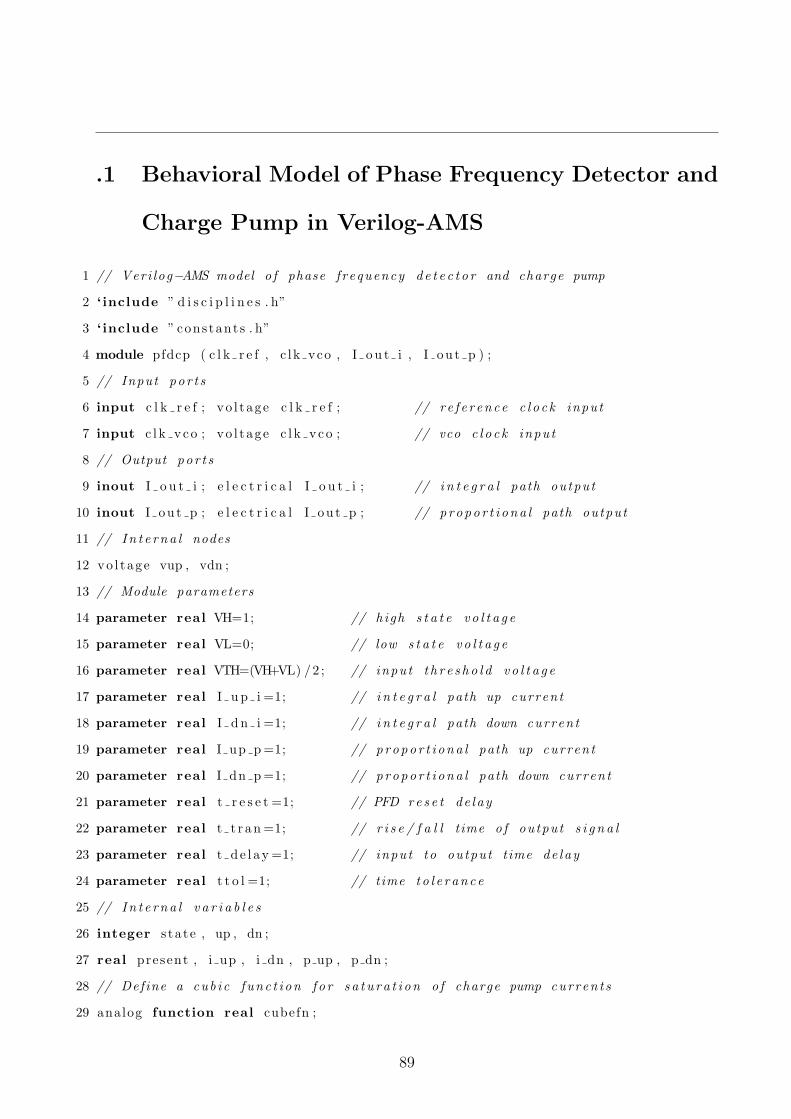
.1 Behavioral Model of Phase Frequency Detector and
Charge Pump in Verilog-AMS
1 // Veri log−AMS model o f phase f requency d e t e c t o r and charge pump
2 ‘ include ” d i s c i p l i n e s . h”
3 ‘ include ” cons tant s . h”
4 module pfdcp ( c l k r e f , c lk vco , I o u t i , I ou t p ) ;
5 // Input por t s
6 input c l k r e f ; vo l t age c l k r e f ; // r e f e r ence c l o c k input
7 input c l k v co ; vo l t age c l k v co ; // vco c l o c k input
8 // Output por t s
9 inout I o u t i ; e l e c t r i c a l I o u t i ; // i n t e g r a l path output
10 inout I ou t p ; e l e c t r i c a l I ou t p ; // p ropo r t i ona l path output
11 // In t e rna l nodes
12 vo l tage vup , vdn ;
13 // Module parameters
14 parameter real VH=1; // high s t a t e v o l t a g e
15 parameter real VL=0; // low s t a t e v o l t a g e
16 parameter real VTH=(VH+VL) /2 ; // input t h r e s h o l d v o l t a g e
17 parameter real I u p i =1; // i n t e g r a l path up current
18 parameter real I d n i =1; // i n t e g r a l path down current
19 parameter real I up p=1; // p ropo r t i ona l path up current
20 parameter real I dn p=1; // p ropo r t i ona l path down current
21 parameter real t r e s e t =1; // PFD r e s e t de lay
22 parameter real t t r an =1; // r i s e / f a l l t ime o f output s i g n a l
23 parameter real t d e l ay =1; // input to output time de lay
24 parameter real t t o l =1; // time t o l e r anc e
25 // In t e rna l v a r i a b l e s
26 integer s ta te , up , dn ;
27 real present , i up , i dn , p up , p dn ;
28 // Define a cub i c f unc t i on f o r s a t u r a t i on o f charge pump curren t s
29 analog function real cubefn ;
89
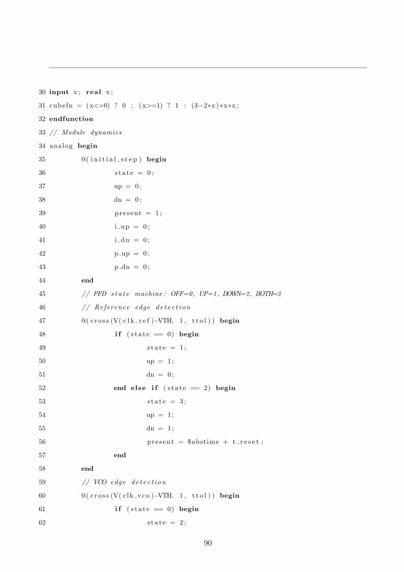
30 input x ; real x ;
31 cubefn = (x<=0) ? 0 : (x>=1) ? 1 : (3−2∗x ) ∗x∗x ;
32 endfunction
33 // Module dynamics
34 analog begin
35 @( i n i t i a l s t e p ) begin
36 s t a t e = 0 ;
37 up = 0 ;
38 dn = 0 ;
39 pre sent = 1 ;
40 i up = 0 ;
41 i dn = 0 ;
42 p up = 0 ;
43 p dn = 0 ;
44 end
45 // PFD s t a t e machine : OFF=0, UP=1, DOWN=2, BOTH=3
46 // Reference edge d e t e c t i on
47 @( c r o s s (V( c l k r e f )−VTH, 1 , t t o l ) ) begin
48 i f ( s t a t e == 0) begin
49 s t a t e = 1 ;
50 up = 1 ;
51 dn = 0 ;
52 end else i f ( s t a t e == 2) begin
53 s t a t e = 3 ;
54 up = 1 ;
55 dn = 1 ;
56 pre sent = $abstime + t r e s e t ;
57 end
58 end
59 // VCO edge d e t e c t i on
60 @( c r o s s (V( c l k v co )−VTH, 1 , t t o l ) ) begin
61 i f ( s t a t e == 0) begin
62 s t a t e = 2 ;
90
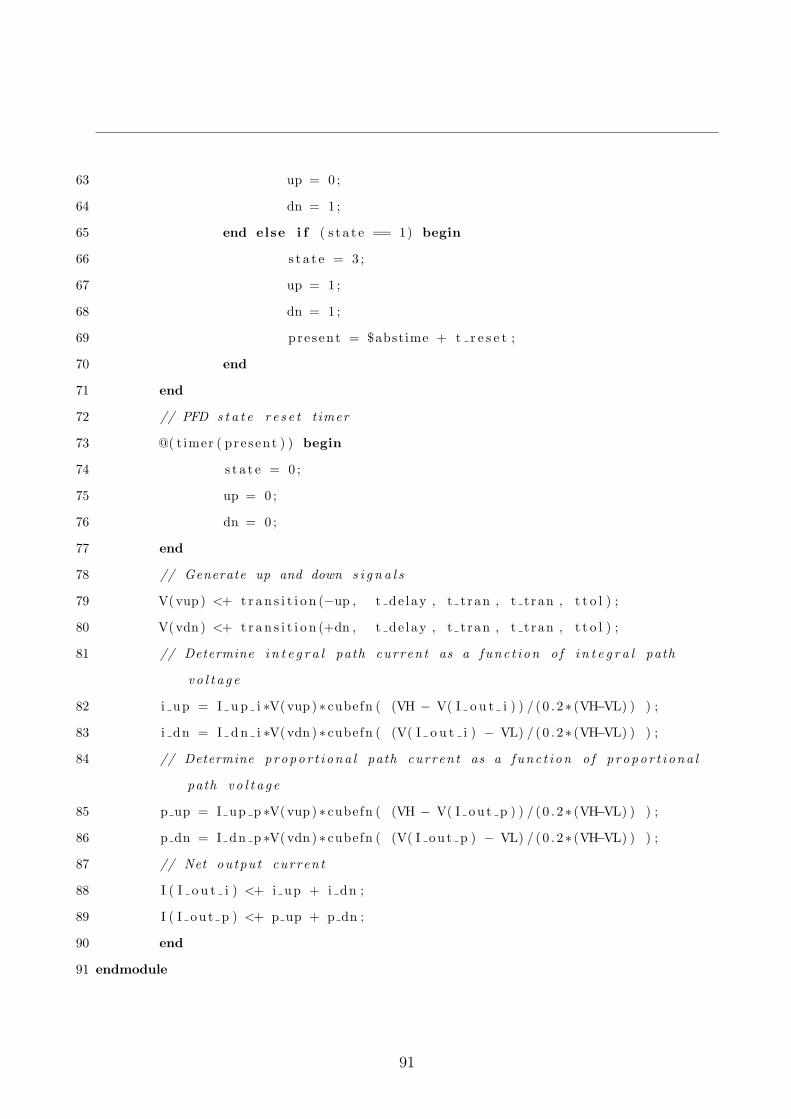
63 up = 0 ;
64 dn = 1 ;
65 end else i f ( s t a t e == 1) begin
66 s t a t e = 3 ;
67 up = 1 ;
68 dn = 1 ;
69 pre sent = $abstime + t r e s e t ;
70 end
71 end
72 // PFD s t a t e r e s e t t imer
73 @( t imer ( pre sent ) ) begin
74 s t a t e = 0 ;
75 up = 0 ;
76 dn = 0 ;
77 end
78 // Generate up and down s i g n a l s
79 V(vup ) <+ t r a n s i t i o n (−up , t de lay , t t ran , t t ran , t t o l ) ;
80 V(vdn ) <+ t r a n s i t i o n (+dn , t de lay , t t ran , t t ran , t t o l ) ;
81 // Determine i n t e g r a l path current as a func t i on o f i n t e g r a l path
v o l t a g e
82 i up = I up i ∗V(vup ) ∗ cubefn ( (VH − V( I o u t i ) ) / ( 0 . 2∗ (VH−VL) ) ) ;
83 i dn = I dn i ∗V(vdn ) ∗ cubefn ( (V( I o u t i ) − VL) / ( 0 . 2∗ (VH−VL) ) ) ;
84 // Determine p ropo r t i ona l path current as a func t i on o f p ropo r t i ona l
path v o l t a g e
85 p up = I up p ∗V(vup ) ∗ cubefn ( (VH − V( I ou t p ) ) / ( 0 . 2∗ (VH−VL) ) ) ;
86 p dn = I dn p ∗V(vdn ) ∗ cubefn ( (V( I ou t p ) − VL) / ( 0 . 2∗ (VH−VL) ) ) ;
87 // Net output current
88 I ( I o u t i ) <+ i up + i dn ;
89 I ( I ou t p ) <+ p up + p dn ;
90 end
91 endmodule
91
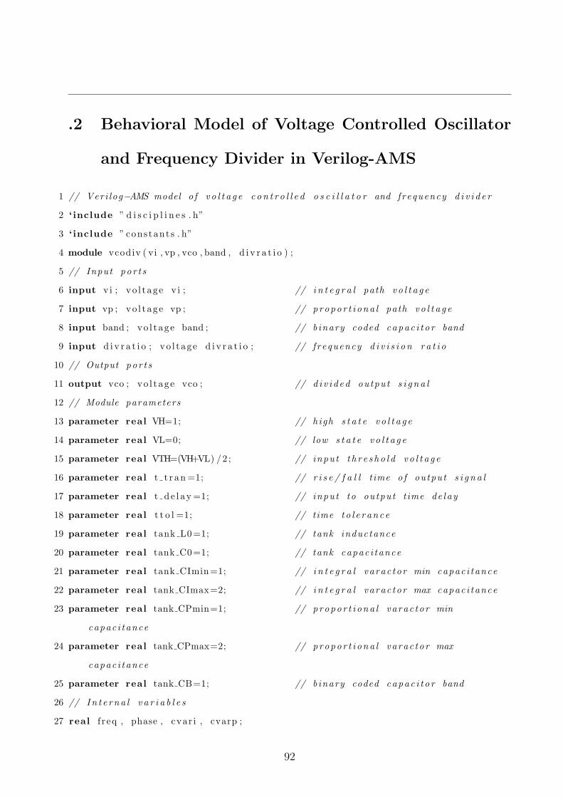
.2 Behavioral Model of Voltage Controlled Oscillator
and Frequency Divider in Verilog-AMS
1 // Veri log−AMS model o f v o l t a g e c on t r o l l e d o s c i l l a t o r and f requency d i v i d e r
2 ‘ include ” d i s c i p l i n e s . h”
3 ‘ include ” cons tant s . h”
4 module vcodiv ( vi , vp , vco , band , d i v r a t i o ) ;
5 // Input por t s
6 input v i ; vo l t age v i ; // i n t e g r a l path v o l t a g e
7 input vp ; vo l t age vp ; // p ropo r t i ona l path v o l t a g e
8 input band ; vo l t age band ; // b inary coded capac i t o r band
9 input d i v r a t i o ; vo l t age d i v r a t i o ; // f requency d i v i s i o n r a t i o
10 // Output por t s
11 output vco ; vo l t age vco ; // d i v i d ed output s i g n a l
12 // Module parameters
13 parameter real VH=1; // high s t a t e v o l t a g e
14 parameter real VL=0; // low s t a t e v o l t a g e
15 parameter real VTH=(VH+VL) /2 ; // input t h r e s h o l d v o l t a g e
16 parameter real t t r an =1; // r i s e / f a l l t ime o f output s i g n a l
17 parameter real t d e l ay =1; // input to output time de lay
18 parameter real t t o l =1; // time t o l e r anc e
19 parameter real tank L0=1; // tank inductance
20 parameter real tank C0=1; // tank capac i tance
21 parameter real tank CImin=1; // i n t e g r a l varac tor min capac i tance
22 parameter real tank CImax=2; // i n t e g r a l varac tor max capac i tance
23 parameter real tank CPmin=1; // p ropo r t i ona l varac tor min
capac i tance
24 parameter real tank CPmax=2; // p ropo r t i ona l varac tor max
capac i tance
25 parameter real tank CB=1; // b inary coded capac i t o r band
26 // In t e rna l v a r i a b l e s
27 real f r eq , phase , cvar i , cvarp ;
92
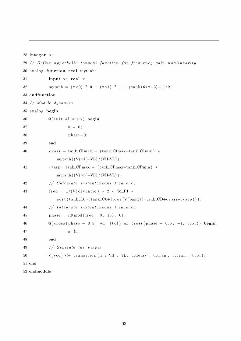
28 integer n ;
29 // Define h yp e r b o l i c tangent f unc t i on f o r f requency gain non l i n e a r i t y
30 analog function real mytanh ;
31 input x ; real x ;
32 mytanh = (x<0) ? 0 : (x>1) ? 1 : ( tanh (6∗x−3)+1) /2 ;
33 endfunction
34 // Module dynamics
35 analog begin
36 @( i n i t i a l s t e p ) begin
37 n = 0 ;
38 phase=0;
39 end
40 cva r i = tank CImax − ( tank CImax−tank CImin ) ∗
mytanh ( (V( v i )−VL) /(VH−VL) ) ;
41 cvarp= tank CPmax − ( tank CPmax−tank CPmin ) ∗
mytanh ( (V(vp )−VL) /(VH−VL) ) ;
42 // Ca l cu l a t e ins tan taneous f requency
43 f r e q = 1/(V( d i v r a t i o ) ∗ 2 ∗ ‘M PI ∗
s q r t ( tank L0 ∗( tank C0+f l o o r (V(band ) ) ∗tank CB+cva r i+cvarp ) ) ) ;
44 // In t e g r a t e ins tan taneous f requency
45 phase = idtmod ( f req , 0 , 1 . 0 , 0) ;
46 @( c r o s s ( phase − 0 . 5 , +1, t t o l ) or c r o s s ( phase − 0 . 5 , −1, t t o l ) ) begin
47 n=!n ;
48 end
49 // Generate the output
50 V( vco ) <+ t r a n s i t i o n (n ? VH : VL, t de lay , t t ran , t t ran , t t o l ) ;
51 end
52 endmodule
93