sem1600 topic 6: a practical introduction to digital power supply · pdf file ·...
TRANSCRIPT

6-1
A Practical Introduction to Digital Power Supply Control
Laszlo Balogh
ABSTRACT The quest for increased integration, more features, and added flexibility – all under constant cost pressure – continually motivates the exploration of new avenues in power management. An area gaining significant industry attention today is the application of digital technology to power supply control. This topic attempts to clarify some of the mysteries of digital control for the practicing analog power supply designer. The benefits, limitations, and performance of the digital control concept will be reviewed. Special attention will be focused on the similarities and differences between analog and digital implementations of basic control functions. Finally, several examples will highlight the contributions of digital control to switched-mode power supplies.
I. INTRODUCTION Power management is one of the most
interdisciplinary areas of modern electronics, merging hard core analog circuit design with expertise from mechanical and RF engineering, safety and EMI, knowledge of materials, semiconductors and magnetic components. Understandably, power supply design is regarded as a pure analog field. But from the very early days, by the introduction of relays and later the first rectifiers, power management is slowly incorporating more and more ideas from the digital world. Ones and zeros are translated to on and offs but at the end a diode can be viewed as a digital component. The introduction of switched mode power conversion required even more digital knowledge seeping into the repertoire of the practicing power supply designers. The know-how of the first discrete implementations of the PWM logic using comparators, gates and latches have faded away long time ago. Integrated pulse width modulator ICs have turned those simple digital circuits to history and have introduced even more digital content to power management.
Todays highly integrated power management ICs are packed with digital gates. The digital circuits allow the integration of some highly sophisticated features. Some examples are EEPROM based trimming after packaging to eliminate package stress related initial offsets,
digital delay techniques to adjust proper timing of gate drive signals, microcontrollers and state machines for battery charging and management, and the list could go on.
If power conversion already incorporates such a large amount of digital circuitry, it is a legitimate question to ask: what has changed? What is this buzz about digital power?
II. GOING DIGITAL Despite the tremendous amount of digital
circuitry used in power management integrated circuits, it remained mainly hidden from the users. Most externally accessible functions are implemented by fundamentally analog circuit blocks today. Thus PWM controllers and other power management integrated circuits have successfully upheld their analog feel to them, making analog measurements and accepting analog controls. Their interfaces to the outside world are the various comparators and amplifiers monitoring the operating conditions and providing a choice of protection options for the designer of the power supply. This elemental principle prevails in existing controllers as demonstrated in Fig. 1.

6-2
PowerStage Filter
LOGIC
OUT
CONTROLLER
IN
SENSORY INPUTS&
COMMAND FUNCTIONS
ADC(PWM) VOLTAGE
&CURRENT
REGULATION
Fig. 1. Top level analog PWM controller architecture.
Another important aspect to notice in Fig. 1 is the fact that the analog inputs are converted to digital signals as soon as practical. The point where the conversion is taking place in todays controllers varies depending on the signal type. When an under voltage lock out function is considered, the conversion is done by the simplest of all analog-to-digital converters, an UVLO comparator. Its input is strictly analog, while the output is already a digital signal, it is either high (1) or low (0), with no intermediate value. But this digital output is also buried inside the integrated circuit and it is very rarely accessible by the designer. Output voltage and current regulation employs closed loop negative feedback, traditionally done by error amplifiers and the conversion to the digital domain is performed by a PWM comparator, again well concealed inside the IC.
A. What Really is “Digital Power”? Digital power is an inaccurate description
of a new direction in the controller design of the power supply to replace the analog circuits by digital implementations. Accordingly, digital power really stands for digital control of the power supply. Digital power supply control attempts to move the barrier between the analog and digital sections of the power supply right to the pins of the control IC.
PowerStage Filter
DIGITALPROCESSOR
OUT
CONTROLLER
IN
SENSORY INPUTS&
COMMAND FUNCTIONS
ADC
VOLTAGE&
CURRENTREGULATION
ADC
ADC
ADC
Fig. 2. Top level representation of a “digital” power supply.
This fundamental change in the control philosophy is summarized in Fig. 2. When comparing Fig. 1 and 2, it is important to emphasize that the deployment of digital control had no effect on the operating principle and the design of the power stage. The specification of the power supply still determines the choice of topology, the selection of power components and the required control functions. That leaves a fair amount of design tasks still in the analog realm for the power supply expert.
B. What is Changing? The striking difference between analog and
digital control is the quality and the amount of information available for the controller to make decisions regarding the operation of the power stage. For example, the output of a comparator carries limited information about the monitored parameter, i.e. only whether it is above or below a threshold. When the border between analog and digital is moved from the output of a comparator to the input by converting the actual information to digital form, the controller suddenly knows the concrete value of the parameter. Now, in addition to comparing it to a threshold, changes in the parameters value can be detected, stored and later reported back to a supervisory system. If necessary, parameter values can be combined

6-3
with other information in complex algorithms to perform even more sophisticated functions.
Of course, this large amount of information can not be processed by traditional logic gates. Digital controllers take advantage of large scale integration offered by state of the art semiconductor technology. Typically, a microcontroller (µC) or a digital signal processor (DSP) is at the heart of a suitable digital controller for power supply applications.
Another important controller property which changes significantly is the flexibility to implement various control algorithms. Traditional, analog controllers may employ sophisticated decision trees driven by the digital outputs of the various peripheral circuits. But the reactions to the changes in the operating conditions are pre-programmed and rigidly executed by the internal logic. For instance, the usual reaction to exceeding a current limit threshold is to shut down the converter and start over, hard coded into the logic of analog controllers. The power supply designer has no option and in most cases it requires a significant amount of external circuitry to circumvent some of the built-in features of the controllers. By the introduction of a digital engine such as a µC or DSP, the decision, how to react to certain conditions becomes user programmable. In the current limit example the designer might opt to let the power supply operate in current limit for a number of switching cycles before resorting to shutdown. This would allow riding through short overload conditions during transient operation. In other cases where this behavior is not necessary or outright dangerous, the controller could be programmed to shut down immediately.
Another area to address in digital control is to ensure stable operation of the power supply. The output voltage is still regulated by a closed negative feedback loop, but it will be the result of complex calculations performed by the µC or DSP. While stability criterias for a power supply with analog control is well established and understood by the designers, these control laws are not directly applicable to the digital controllers. The digital implementations require new expertise, being familiar with and being able to apply the stability requirements in the
Z-domain. The Z-domain transfer function of a sampled data system can be used to predict the small signal behavior of the converter. Additional new problems surface as well, like bandwidth limitations, resolution issues in time and voltage measurements and limit cycle oscillation, just to mention a few which will be discussed later.
One more key aspect of digital implementations is to recognize that microcontrollers and DSPs are powered by very low voltages due to their semiconductor technologies. As a result they are not capable of directly interfacing with the power components, unlike their analog counterparts. Thus, they require their own low voltage supply and a suitable high current gate driver with a compatible input threshold and adequate output voltage range. These requirements establish a clear partitioning between the analog and digital sections of the power supply. A closer look of the fundamental architecture of a digitally controlled converter is shown in Fig. 3.
BIAS
LOW VBIAS
VIN
POWER STAGE
uC or DSP
COM
DIGITAL
ANALOG
Fig. 3. Analog – digital boundary in a power supply.
The low voltage bias shown in Fig. 3 must be able to power the digital controller independently without operation of the power stage to allow initialization during start-up and to preserve intelligence during standby (disable) and short circuit operation when traditional bootstrap bias might not be available as a viable power source.

6-4
Furthermore, the output of the digital controller must be converted to a suitable signal to drive the power switches in the converter and all voltages must be scaled to the input voltage range of the analog inputs, usually determined by the reference voltage of the analog-to-digital converter on-board the digital controller.
C. Advantages of Digital Control Flexibility is definitely the most noteworthy
benefit of digital controllers. It is especially remarkable considering the consolidation of all necessary functions into one highly integrated, sophisticated controller. As mentioned before, by the introduction of a digital controller, the hardwired, hardly customizable control flow of analog controllers is exchanged for an open structure, where the designer has the ultimate freedom to decide the right course of action to a given stimuli. This new opportunity can be rather overwhelming for practicing power supply designers, because most of these decisions were made for them by the semiconductor manufacturers of analog controllers. In addition, this freedom comes with another new complication, the digital controller must be told what to do. Software must be written to program the execution of all the functions assigned to the µC or DSP. The software carries the knowledge and intellectual property which was previously realized in the controller hardware.
There are three major areas in the design where flexibility can provide significant benefits. The first one is adjustability. Every parameter which is measured or programmed can also be adjusted by the digital controller. These include voltage and current thresholds, operating frequency, thermal shut down, startup time, and so on.
The next level of flexibility is offered by the user defined what-if decision making process inside the digital controller. This tool can be exploited for enhanced functionality like green mode or low power stand-by operation, load share or hot swap control, just to mention a few. The foundation of these features is the option to invoke different control algorithms as the operating conditions of the power supply are changing. In addition, fault containment
strategies can be refined and adapted as required by diverse applications. For example, once the output current of the converter is measured by the digital controller this information can be used to program fold back, constant power, constant current, delayed shutdown or any other mode of over current protection. Moreover, any combination of these output characteristics can be implemented without ever changing any components in the power supply.
The use of modern digital controllers also adds communication as a potential feature to the power supply. When this communication capability is utilized, the flexibility of the digital approach is greatly enhanced through the on-the-fly programmability. The adjustability of the converters output voltage is a great advantage as demonstrated in processor applications using VID code. In a communication enabled power supply, not just the output voltage, but current limit, operating frequency and other vital operating parameters become programmable by a host system during operation. Beyond programming, communication permits remote data logging of the operating conditions of the power supply. By examining the data such as efficiency, output ripple, temperature rise, certain shifts in the measured parameters may be the leading indicators of pending failures. These trends can be used for failure prediction, down-time avoidance and intelligent fault management. In a centrally managed power supply, start-up, shut-down and sequencing can also be supervised remotely by a higher level supervisory system.
All these options and the corresponding computing power on-board can open the door for customization of future power supplies and entire power systems through software. This approach promotes platform development and a faster Time to Market window. Despite the potential standardization of the hardware, digital control allows unique product differentiation through software. The implementation methods of the various power supply features remain well protected due to the software code security feature of modern microcontrollers and DSPs which ensures that the program can not be read by unauthorized users.

6-5
In complex systems such as the telecommunication power infrastructure or high end computing environments, digital control also offers reduced component count even with the increased functionality. Fewer components mean lower manufacturing cost and higher reliability.
It is important to note though that all this flexibility and adjustability is restricted by the capabilities of the power stage. For example, widely varying output voltages might require different turn ratios in the transformer and filter inductors must be selected with the maximum output current in mind. Lowering the operating frequency still increases output ripple although it might improve light load efficiency. All these effects of the adjustable parameters must be carefully considered otherwise the performance of the power supply can be significantly penalized. But it is possible to use the same digital controller with several versions of the power stage, taking advantage of its ultimate flexibility.
D. Present Status of Digital Control in Power Management The digital revolution is in its early phase
in power supply applications. Its present state resembles the motion control and UPS field just some 20 years ago. The first digital controllers operated at moderate switching frequency and debuted in those applications in the early 80s.
The digital control acceptance rate was relatively slow, despite the fact that the technology was readily available and capable of performing the job. Microcontrollers and DSPs had sufficient computing power to handle speed control, sine wave generation and other similar low speed control function. In addition they offered the possibility of communication between a host supervisor and the equipment. As the performance has improved and the price of the digital controllers has dropped during the years, the technology became standard in most motor control and large UPS systems.
Digital control in power management is gaining considerable attention in recent years in
academia and in the industry as well. Numerous publications in major conferences discuss the theoretical and practical aspects of digital control implementations. Significant interest of the subject had been expressed at APEC 2003 where the first Rap Session on digital power took place with participation from end users, power supply manufacturers and IC companies. The first Market Report was published by iSupply on digital power in early 2003.
A closer look at the reported results confirms that in power supplies, digital technology might not yet be ready for prime time. Some of the problem stems from the ever present price pressure the industry is operating under. Like any new technology, digital controllers cost more until reasonable sales volume is reached. Reaching a sufficient level of production is delayed by the required time to learn and introduce new design disciplines and to address manufacturing needs associated with digital controllers. Also hindering the effort is the lack of appropriate analog support components to go along with the microcontroller or DSP.
On the theoretical front, the majority of present implementations translate S-domain transfer functions to Z-domain. This approach permits utilization of the well understood linearized small signal model of the power supply. Once the poles and zeros are calculated to ensure the stability of the system, the Z-coefficients of the digital transfer function can be found easily. The weakness of this method is that by starting from a linearized model, the benefits of a higher performance non-linear control theory can not be fully utilized. As a result, the performance of power supplies using either digital or analog controllers are very similar today.
To set realistic expectations of todays digital implementations in power supplies, Table 2 attempts to highlight the pros and cons of the analog and digital approaches.

6-6
TABLE 1. COMPARISON OF ANALOG AND DIGITAL CONTROLLER PERFORMANCE (+ BETTER; - WORSE)
Control Properties Analog Digital
Switching frequency (CPU limitations) + -
Precision (tolerances, aging, temperature effects, drift, offset, etc.) - + Resolution (numerical problems, quantization, rounding, etc.) + - Bandwidth (sampling loop, ADC DAC speed) + - Instantaneous over current protection + - Compatibility with power components + - Power requirements + - Communication, data management - +
Understanding theory + -
Advanced control algorithm (non-linear control, improved transient) - + Multiple loops - +
Cost of controller + -
Cost of a platform (flexibility, time to market) - + Component count (comparable functionality, integration) - + Reliability + ?
Achieving high switching frequency is
definitely easier using analog controllers. Obtaining high enough clock frequency to implement direct digital pulse width modulation with reasonable resolution is the fundamental problem. Todays digital controllers with suitable clock speed for high switching frequency operation are not cost effective and consume a significant amount of bias power. Another area where speed is critical is the performance of the digital controllers analog-to-digital converter. The ADCs conversion time and the number of instructions needed to acknowledge the result have an effect on the digital controllers performance. Where sensing and reacting to certain conditions should happen simultaneously peak current limiting for example analog circuits still has a significant advantage over pure digital implementations. Furthermore, the repetition rate of converting important parameters like output voltage, impacts the bandwidth of the control algorithm. An additional important characteristic of the analog-to-digital converter is its resolution which can introduce rounding or quantization errors. These numerical issues are inherent in digital control and represent a new challenge for the power supply designer. On a positive note, digital components can offer better
accuracy, great resilience against temperature drift and aging effects. Digital controllers are a better fit to implement advanced control algorithms and to manage multiple control loops if necessary.
In the most important comparison cost digital power supply control can be competitive. If all the functions provided by a digital implementation are necessary to meet specification, digital controllers will come out on top. In this case, component count and cost will be significantly lower than the cost of analog control circuits and the required additional support ICs to accomplish comparable features. When the only task is to regulate an output voltage, digital controllers might have a hard time competing on price. In this instance, a bigger picture should be considered to evaluate the real advantages of a digital implementation. If the design is expected to be re-used in several power supplies, the flexibility and possibility of quick modifications in software is a very valuable attribute of the digital implementation although it could be difficult to identify its cost benefit.
Finally, reliability is a key question. Analog controllers have a proven track record in power supply applications. They work reliably in harsh, noisy environment. Digital controllers have

6-7
proven to be very reliable as well, but not necessarily inside a power supply. It is unclear whether microcontrollers and DSPs will operate reliably under the same circumstances.
III. DIGITAL BASICS To fully understand the potential benefits of
digital control, some basic operating principles and terminology must be clarified. The two fundamental building blocks to understand are the time base and how the analog signals are converted to digital form. These two circuits interface with the surrounding analog world and are critical to the digital controllers performance.
A. Generating the Time Base One of the first steps in the design procedure
is to establish the operating frequency of the controller. It is usually defined by an on-board oscillator, often programmed by R-C timing components. A frequently used implementation of a simple analog oscillator is shown in Fig. 4.
Q
Q
R
S
VPEAK
VVALLEY
fSW
V+
Fig. 4. Analog oscillator.
PERIODREGISTER
n
n
COUNTER
CO
MPA
RE
fSWfCLK
RE
SET
Fig. 5. Simplified digital oscillator (fCLK >> fSW).
Since the R and C values can be set to any desired value, this oscillator can run at any frequency within its wide operating range. In an analog implementation the controllers clock frequency and the converters operating frequency (fSW) are the same.
On the other hand, the clock frequency (fCLK) of a microcontroller or a DSP is much higher than the actual operating frequency of the converter. The digital controller uses fCLK as the time base for the central processor unit and its peripherals only. All other timing functions, including the switching period, must be generated using the internal resources of the digital controller.
Fig. 5 demonstrates the principle of deriving the switching frequency. Once the clock frequency of the digital controller and the switching frequency of the converter are fixed, the switching period can be established. The number of clock cycles in the switching period can be calculated by dividing the switching period by the clock period. This number is stored in the period register. Every clock signal increments the counter by one and eventually the counter value will be equal to the period. At that time the digital comparator produces an output pulse which will reset the counter to zero. The frequency of the comparator output pulse is also the desired operating frequency of the converter.
As fCLK increases with respect to fSW, more clock cycles become available within a switching period to perform the complex arithmetic calculations, data conversions and housekeeping functions. This indicates that the higher clock frequency has a desirable effect on the performance of the digital controller.
Another important reason to push the clock frequency higher becomes clear when the relationship between the number of clock cycles in a switching period and the PWM resolution of the digital controller is investigated. An analog controller can command any pulse width as the decision is made using analog signals providing infinite resolution. In a digital controller the PWM pulse width is represented by an integer number of clock cycles calculated by the arithmetic unit, therefore the pulse width has a finite number of discrete values.

6-8
TABLE 2. EFFECTIVE NUMBER OF BITS, NUMBER OF CLOCK CYCLES PER PERIOD AND DUTY CYCLE RESOLUTION IN %, USING TYPICAL COMBINATIONS OF SWITCHING AND CLOCK FREQUENCIES
fSW fCLK - Clock Frequency (MHz) (kHz) 1 2 4 8 20 40 100 150
5.3 6.3 7.3 8.3 9.6 10.6 12.0 12.6 Bit resolution (eff.) 25 40 80 160 320 800 1600 4000 6000 Clock cycles/period 2.50 1.25 0.625 0.313 0.125 0.063 0.025 0.017 D resolution (%) 4.3 5.3 6.3 7.3 8.6 9.6 11.0 11.6 Bit resolution (eff.)
50 20 40 80 160 400 800 2000 3000 Clock cycles/period 5 2.50 1.25 0.625 0.250 0.125 0.050 0.033 D resolution (%) 3.3 4.3 5.3 6.3 7.6 8.6 10.0 10.6 Bit resolution (eff.)
100 10 20 40 80 200 400 1000 1500 Clock cycles/period 10 5 2.50 1.25 0.50 0.25 0.10 0.067 D resolution (%) 2.0 3.0 4.0 5.0 6.3 7.3 8.6 9.2 Bit resolution (eff.)
250 4 8 16 32 80 160 400 600 Clock cycles/period 25 12.5 6.25 3.125 1.250 0.625 0.250 0.167 D resolution (%) 1.0 2.0 3.0 4.0 5.3 6.3 7.6 8.2 Bit resolution (eff.)
500 2 4 8 16 40 80 200 300 Clock cycles/period 50 25 12 6.25 2.50 1.25 0.50 0.333 D resolution (%) 0.0 1.0 2.0 3.0 4.3 5.3 6.6 7.2 Bit resolution (eff.)
1000 1 2 4 8 20 40 100 150 Clock cycles/period 100 50 25 12.5 5.0 2.5 1.0 0.667 D resolution (%)
The pulse width of the digital controller can
only be multiples of the clock period. The important characteristics of the digital PWM engine can be defined as a function of the switching frequency and the clock frequency as shown in Table 2.
For every combination there are three numbers in the table. The first number is called the effective number of bits and it signifies how many bits are required in the counter to be able to set up the desired switching frequency with a given clock frequency. The second number indicates how many clock cycles are available in a switching period. And the third number, which can be defined as:
100ff(%)D
SW
CLKRES ⋅=
gives the duty cycle resolution in percentage which is the most important parameter determining the performance of the digital controller. Due to the distinct values of the duty ratio of the digital controller, the output voltage of the converter can not be adjusted continuously. Depending on the difference between two
neighboring duty cycle values, the output voltage resolution is also affected. A further variable to define how coarse the output voltage adjustment will be is the steady state operating duty ratio at nominal input, output conditions (DNOM).
10.80.60.40.200
2
4
6
8
10
Steady State Operating Duty Cycle (DNOM)
VO
,NO
M, N
orm
aliz
ed O
utpu
t Vol
tage
Cha
nge
[%]
Duty Cycle Resolution (DRES):
0.0010.0050.010.02
Fig. 6. The effect of duty cycle resolution on the output voltage resolution as a function of nominal operating duty ratio.

6-9
In Fig. 6, the curves represent the percentage of output voltage change in response to changing the converters duty ratio between two neighboring discrete values. It is important to remember that the time difference between two neighboring duty ratio values is constant and it equals 1/fCLK. As Fig. 6 emphasizes, the same duty cycle step will result different output voltage changes depending on the nominal operating duty cycle of the converter. In other words, increasing the conduction time of the power supplys main switch by one clock period (1/fCLK) at narrow operating duty ratio will raise the converters output voltage more than the same change applied at wider nominal duty cycles. Therefore, in converters typically operating with narrow duty cycles for example a 12V to 3.3V non-isolated buck converter it is desirable to have a higher speed (fCLK) digital controller even at moderate switching frequencies.
To further underline the impact of the duty cycle resolution, consider the above mentioned buck converter as an application example. The converter operates at 250kHz switching frequency using an 8 MHz digital PWM engine. The input is 12V and the output voltage is 3.3V. The required operating duty ratio would be:
275012
33V
VDIN
OUTREQ .. ===
The corresponding PWM pulse width is:
s11kHz250
2750f
Dt
SW
REQON µ.. ===
This requires; 88MHz8s11ftn CLKONON .. =⋅=⋅= µ
number of clock cycles. Since the digital controller can not put out fractional number of clock cycles, the on-time will be the closest integer number of cycles, nine. This duty cycle will yield an output voltage of:
V3753MHz8
kHz2509V12ffnVVCLK
SWIN9nO .)( =⋅⋅=⋅⋅==
While this value might satisfy the requirements of the design (+2.2%), it is important to determine what the output voltage would be at neighboring duty ratios:
V003MHz8
kHz2508V12ffnVVCLK
SWIN8nO .)( =⋅⋅=⋅⋅==
V753MHz8
kHz25010V12ffnVVCLK
SWIN10nO .)( =⋅⋅=⋅⋅==
The calculations show a 0.375V or 11.1%
output voltage step in response to a duty cycle change of one clock period which is clearly not acceptable. A visual representation of the output voltage and discrete duty cycle values around the nominal output voltage is shown in Fig. 7.
RegulationWindow
VO,MAX
VO,MIN
V O, O
utpu
t Vol
tage
[V]
Analog (D) and Discrete (DX) Duty Cycle0.340.300.260.22
2.5
2.9
3.3
3.7
4.1
4.5
n=9D9=0.281n=8
D8=0.25
n=10D10=0.312
Fig. 7. Output voltage vs. duty ratio in digitally controlled power supply.
Another instance where discrete duty cycle values can be observed is the effect of input voltage change on the output voltage of the converter. Utilizing the infinite resolution of analog controllers, the output voltage is regulated practically at a constant level, independently from the input voltage. With only a finite number of duty ratios being available in digital control the output voltage can not be held at a constant value. Fig. 8 shows the example converters output voltage as a function of VIN around the nominal 12V value.

6-10
VO,MAX
VO,MIN
VO, O
utpu
t Vol
tage
[V]
3.0
3.1
3.2
3.3
3.4
3.5
3.6
VIN, Input Voltage [V]13121110 14
n=9D9=0.281
n=8D8=0.25
n=10D10=0.312
Fig. 8. Output voltage vs. input voltage in digitally controlled power supply.
Due to the finite number of possible duty ratios the converters output voltage will be proportional to the input voltage until the operating conditions will demand the next smaller duty cycle. At that moment the output voltage suddenly drops to the new value corresponding to the new duty ratio as demonstrated in Fig. 8.
B. Digitizing Variables – Voltage Sense In addition to the effects of discrete time
steps the various control variables are also digitized in the digital controller. This introduces another level of complexity in the design. First of all it is important to note that the digital controller measures everything as a voltage input connected to an on-board analog-to-digital converter, usually through a multiplexer. All voltages monitored by the ADC must be scaled to the input voltage range of the ADC, generally between ground and the reference of the ADC. Typical reference levels are either 1.25V or 2.5V and these references can be internal or external to the analog-to-digital converter. After the conversion, the measured voltage level will be represented by a digital value as shown in Fig. 9.
MUX A-to-D 1 0 1 1 0….2 13n n-1
2021222n-22n-1
IN1IN2
IN5IN4IN3
+
Fig. 9. Voltage measurement using ADC.
The analog-to-digital converter can be characterized by the number of bits of its output and by the time required to produce the result. The ADCs number of bits is directly related to the accuracy of the measurement because it defines the resolution. When the input signal to the ADC is equal to (or larger than) its reference voltage all output bits will be 1. From this relationship the resolution of the ADC can be calculated according to:
nREF
ADC 2Vres =
where n is the number of bits of the analog-to-digital converter. That means that the input voltage range is divide into 2n number of equal bands and the ADC identifies the band containing the amplitude of the input signal. In order to establish the resolution of the actual measurement the gain and accuracy of the external resistive divider needs to be taken into account as well. For instance, measuring the 3.3V output of the earlier introduced example using an 8-bit ADC with a 1.25V reference will require a 3:1 divider in front of the input of the analog-to-digital converter. Notice that the 1.25V should not be used as an equivalent of the 3.3V because potential over voltage conditions could not be sensed. The 3:1 divider will allow measurement of the output voltage in the 0V to 3.75V range. Now the resolution of the output voltage measurement can be established as:
nFS
Vo 2Vres =
where VFS is the full scale amplitude and n is the number of output bits of the ADC. In our example the output voltage resolution is:
mV6142
V753res 8Vo .. ==

6-11
This means that the converters output voltage can change as much as 14.6mV before it will become evident at the output of the analog-to-digital converter and the duty cycle could be modified. The ambiguity introduced by the measurement resolution ultimately impacts the regulation accuracy in power supply applications. The worst case error can be calculated by the following expression:
100V2
VinEO
nFS
RES ⋅⋅
=%)(
Substituting the already familiar values from our example yields:
%..
.%)( 440100V332
V753inE 8RES ±=⋅⋅
=
This inaccuracy is additional to the error introduced by the tolerance of the reference and the resistive divider which scales the output voltage level to the input range of the ADC.
Theoretically, using more bits in the analog-to-digital converter increases the resolution and consequently the measurement accuracy as shown in Table 3.
TABLE 3. ADC ACCURACY AS A
FUNCTION OF BITS ADC
Number of bits 8 10 12 14 16
ERES (in %) 0.444 0.111 0.028 0.007 0.002
Another property of the analog-to-digital
converter which deserves attention is the time needed between the command initiating the measurement and when the result is available in the output register of the ADC. This period consists of two intervals, the actual time needed to convert the analog signal to a digital word plus the number of instructions used to process, store and read the result. Since most modern microcontrollers and DSPs can access the result in a single instruction cycle, the most important parameter is the conversion time. Usually the conversion time is given indirectly by specifying the number of conversions in a second. For example, 200ksps (kilo-samples-per-second) performance translates to 200,000 conversions in a second, i.e. 200kHz. That means that the
conversion time is around 5µs. Since the ADC is an autonomous peripheral, the microcontroller or DSP can perform other tasks during the conversion.
The conversion time is important for two main reasons in power supply applications. The first problem is that the conversion time can be considered as a time delay. Its effect is similar to having a very slow comparator in an analog controller. There are plenty of functions in a power supply where this is acceptable like under voltage lockout, but it is certainly not adequate where quick response to a fast changing parameter is critical, such as for current protection or even for peak current mode control. In general, it can be said that digital controllers can not replicate the instantaneous reaction of the analog controllers due to the time lag of the ADCs conversion time.
The other aspect of the conversion time is related to the bandwidth of the control loop. The sample frequency, how often the output voltage can be measured, will be seriously impacted by the conversion time of the analog-to-digital converter. In an analog implementation the output voltage is sampled in every switching cycle. If similar performance is expected from the digital controller, the switching frequency must be equal or less than the maximum frequency which can be supported by the ADC. Even then it should be assumed that the output voltage is the only parameter the ADC is measuring which is clearly not the case in most power supply applications.
C. Digital Pulse Width Modulation Now that some of the basic blocks and
characteristics of a digital controller have been introduced, the operation of the analog and digital pulse width modulator can be compared. Fig. 10 illustrates the fundamental process to obtain the operating duty ratio of a power supply using an analog (top drawing) and a digital (bottom drawing) approach.
The analog control circuit requires a reference, an error amplifier and a comparator to determine the required duty cycle. As shown in Fig. 10, the output voltage is compared to a reference using a resistive divider at the inverting
6-12
input of the error amplifier. The control law is also implemented by the error amplifier by selecting the appropriate R and C values to set the poles and zeros of the differential equations governing the behavior of the negative feedback loop. The actual duty cycle is produced by a simple comparator by comparing the error voltage to an artificial ramp which also carries the information of the operating frequency of the circuit. The duty cycle generated this way can be any value allowing the analog controller to regulate the output voltage of the power supply exactly at the desired amplitude.
VO(A)
VERROR
DA
ADC
VREF
VREF
VO(D)
Compensation
ALU
fSW, PWM,Compensation
DD
VO(A)
PWM
fCLK
fSW
+
+
Fig. 10. Comparison of analog and digital PWM implementation.
The digital implementation of the pulse width modulator starts with a similar resistive divider which scales the output voltage to the input voltage range of the analog-to-digital converter.
As mentioned before, the input voltage of the ADC at nominal output voltage must be less than VREF to accommodate output voltages above the nominal value during transient operation. The ADC then converts the output voltage to a representative digital word labeled as VO(D) in Fig. 10. The Arithmetic and Logic Unit (ALU), the digital core of the microcontroller or DSP takes care of the rest of the functions. It can establish the switching frequency from the clock frequency of the processor (fCLK) and it will calculate a value for the power supply duty cycle (DD). The digital representation of the nominal output voltage and some of the previously measured VO(D) values are stored in memory and available for a comparison to the most recent output voltage level produced by the ADC. The control law is also executed by the digital engine as programmed by the software.
Without going into digital control theory, the Z-domain control function of our example buck converter which implements the equivalent of two poles and two zeros for a typical type 3 compensation can be written in the following form:
5Kz4Kz3Kz2Kz1KZG 2
2
+⋅−+⋅−⋅=)(
This equation closely resembles the usual S-domain transfer function of the power supply. The computations to execute this control law in the digital domain can be summarized by the next two equations where n refers to the present cycle, n-1 and n-2 are the values from the previous two calculations respectively. The first step is to calculate the error between the desired and measured output voltage:
)()( , nVVnE ONOMO −= Using the just calculated value of E(n) and its
earlier values from the previous two cycles along with the respective duty cycle values (from the memory of the digital controller) the new duty cycle D(n) can be computed:
)()()()()()( nE0b1nE1b2nE2b1nD1a2nD2anD ⋅+−⋅+−⋅+−⋅+−⋅=

6-13
The coefficients of the equation can be obtained by simple mathematical manipulations from the S-domain transfer function or synthesized directly from the component values of the power supply. These constants are stored in the memory of the digital controller and as such can be easily modified during debug or even while the power supply is running according to a specific mode of operation.
D. Limit Cycle Oscillation To ensure stability with a digital controller,
there are two fundamental requirements which must be satisfied. The first one is the traditional small signal stability criteria which is addressed by the appropriate selection of the various constants in the control law equations.
The second constraint involves the time domain resolution of the digital PWM engine and the voltage resolution of the analog-to-digital converter. This unique problem is demonstrated in Fig. 11.
VO=OK VO,NOM
VO
D
VO=high
VO=lowADC
reso
lutio
nPW
Mre
solu
tion
Fig. 11. Demonstration of limit cycle oscillation with digital control.
Assume that the power supply is running in steady state operation with a constant duty ratio producing an output voltage which is in the zero error bin (VO=OK). When the operating conditions change the input voltage increases or some of the load is removed the output voltage starts to climb. Slight output voltage variation is allowed and will not change the duty cycle as long as VO stays within the VO=OK band because the analog-to-digital converter will produce the same result. As soon as the output goes higher than the upper threshold of the zero error bin, the ADC output will change which indicates that the
output is too high. The digital controller mimics the reaction of any analog controller under the same circumstances and will try to compensate by decreasing the duty ratio. The minimum change in the duty ratio is a function of the clock period of the digital PWM engine. In Fig. 11 a situation is depicted where shortening the on-time of the main power switch by one clock period (1/fCLK) results a new output voltage in the VO=low band. This will initiate a correction asking for the next larger duty cycle value which will bring the output voltage back to the VO=high band. And the cycle starts again, the output voltage will oscillate. The smoothing of the output voltage waveform in Fig. 11 is accomplished by the averaging L-C output filter of the power supply.
The obvious problem in this example is that the time domain resolution is too course with respect to the resolution of the analog-to-digital converter. This phenomenon is called limit cycle oscillation and it can happen regardless of whether the design meets all conventional stability criteria. The solution to this dilemma is to follow a design procedure where the ADC resolution is selected first, based on the required accuracy of the output voltage regulation. The duty cycle resolution is then adjusted to the ADC resolution by selecting an appropriate clock and switching frequency combination.
IV. PROGRAMMABLE FUNCTIONS AND VARIABLES
The development of a suitable power supply controller is primarily driven by the answers for three fundamental questions: • What functions to provide? (in addition to
fSW, and PWM) • How to implement them? • When to execute them?
With an analog approach, the first two questions are answered by selecting the PWM controller and some auxiliary components to match the intended features. Once the components are chosen and interconnected, the functions and the control algorithm are fixed and the circuit becomes dedicated to the particular application. Any change in functionality would require adding more components or redesigning

6-14
the interaction among the different sections of the controller. Finally, the voltage levels and limits are set according to the predefined or user adjustable thresholds and by fixed external components. This will define permanently when the functions will be carried out.
On the other hand, the hardware of the digital controller is designed almost independently of its functionality. Only the selection of the input parameters might impact the available functions and their implementation. Practically, all three questions are answered by the programming of the microcontroller or DSP. The software can integrate selected subroutines to address the necessary control functions. The control algorithm can be based on complex decisions evaluated by the digital controller and it can be easily modified by changing a few lines of code in the programming. The different thresholds and limits are also defined in the software as variables and their value can be modified easily. Through this mechanism, many operating parameters of the power supply can be customized without ever changing any component value in the circuit.
Accordingly, programmability and flexibility are the most significant differentiators in favor of the digital power supply controllers.
A. Miscellaneous Control Functions With a powerful processor, the digital
controller is capable of performing many more functions beyond the basic voltage regulation task. By measuring just a few more working parameters of the power supply, a host of intelligent control and protection functions can be implemented. Some of the data and variables which can be easily made available for the digital controller through its analog-to-digital converter or by values stored as variables in memory are: • Input voltage • Average input current • Average output current • Operating temperature • Other output voltages in the system • Host supervisor with serial bus
communication capability • DC Transfer function of the converter • Variable examples:
- VOUT - VOVP - IOUT,MAX - POUT,MAX - VIN,MIN - VIN,MAX - IIN,MAX - IPK,MAX - fSW - DMAX - V·s MAX - DMIN - tSS (soft-start time) A partial inventory of the possible functions
using these additional measurements and variables is summarized in the following list: • Switching frequency modulation • Input voltage monitoring (UVLO, line OVP) • Shutdown, Enable • Soft-start profile • Sequencing sync. rectifier control • DMAX limit • Volt-second clamp • Green mode operation (burst mode, DMIN
limit) • Transient overload response • Current limit profile • Output characteristic (droop, constant power) • Temperature protection (derating, shutdown) • Communication
Since these functions would be implemented in software, the behavior of the system could be tailored to specific applications rather easily. Thats where the flexibility of the digital controller would be the most valuable in contrast to the hard wired responses of analog controllers.
Switching Frequency Modulation Because the operating frequency is defined
by the digital controller, it can be managed through software. There are several applications where variable frequency operation can be beneficial. Off-line power supplies can take advantage of spreading EMI noise spectrum by slowly modulating the switching frequency of the converter in a relatively narrow band around the nominal operating frequency. This could reduce input EMI filter requirements, offer smaller size and lower cost. Another application where this

6-15
opportunity might be welcomed is to meet green mode power consumption limit in standby. In most green mode implementations high efficiency, low power standby mode is facilitated by reduced switching frequency or by burst mode operation, both achievable by controlling the switching frequency using the digital controllers software routines.
Input Voltage Monitoring Knowing the input voltage of the converter
allows the digital controller to accomplish some additional control functions. The most basic ones are line under voltage lock out (UVLO) and line over voltage protection (OVP). To realize these functions, the valid input voltage range of the converter is stored in the digital controllers memory and the measurement is compared to those limits. When the input voltage is outside of the operating range, the power stage is disabled and all other operations of the controller can be suspended. This technique allows low power operation of the microcontroller or DSP because its clock frequency can be significantly reduced. It is also possible for the microcontroller to enter standby mode between measurements since all other tasks are put on hold until the input voltage returns to the nominal range.
Some of the more sophisticated functions based on the actual input voltage level could be brown out protection when the converters input power is limited during brown out conditions.
Another option is to implement an advanced volt-second clamp to protect the transformer from saturation in isolated topologies. When volt-second clamping is employed in analog controllers, designers often face the trade off between fast transient response and effective protection due to the duty cycle limiting effect of the volt-second clamp. The ultimate flexibility of the digital control algorithm could help to overcome this trade-off according to the flow chart shown in Fig. 12.
START DPWM
CALCULATEDVS
DPWM>DVS
COUNT=COUNT+1
COUNT>5
SETDLIM=DVS
YES
YES
NO
NO
CALCULATEDPWM
START V*S
END V*S
READDVS
DPWM>DLIMNO
SETCOUNT=0
SETDLIM=DMAX
END DPWM
YESSET
DPWM=DLIM
READVOUT
MEASUREVIN
STA
TIC
V S
RO
UTI
NE
PW
M R
OU
TIN
ED
YN
AM
IC V
S R
OU
TIN
ED
MAX
RO
UTI
NE
Fig. 12. Advanced volt-second clamp routine.

6-16
Isolated converters frequently adhere to a maximum duty cycle limit (DMAX) especially if they employ a single ended topology. DMAX is usually set during the power stage design and corresponds to operation at minimum input voltage. At that point DMAX=DVS, the volt-second duty ratio limit, calculated as a function of the input voltage. At higher input voltages the volt-second limit reduces the maximum operating duty cycle according to:
21NN
VVD
S
P
IN
OUTVS .⋅⋅=
In this equation the volt-second clamp is set 20% above the nominal duty ratio of the converter as indicated by the 1.2 multiplier. The lower of DMAX or DVS limits the actual duty ratio calculated by the controller based on the output voltage error (DPWM). In normal, steady state operation none of these limits impact the operation of the power supply.
The software routine illustrated in Fig. 12 would allow the converter to operate beyond the volt-second limit for 5 cycles to accommodate fast transient response before cutting back the allowable maximum duty ratio to protect the converter. During the five transient cycles this example uses DMAX to limit the maximum operating duty ratio but the software could be easily modified to provide more protection if needed.
Since the input voltage change is relatively slow, it will not be sampled in every switching period to save computing resources. Therefore, the static volt-second routine is independent from the PWM calculation as shown in Fig. 12 and once it is executed, its result can be used until the next calculation is completed.
Current Sense The digital controller can also measure the
input, output or both currents of the power supply. The collected current information can be utilized to implement various types of current limiting methods or can be combined with other parameters to customize the power supplys output characteristic under overload conditions.
The most frequently used current limit techniques include: • Constant output current • Foldback • Transient ride through (delayed shutdown) • Hiccup (shut down & retry) • Shutdown (permanent lock out)
When foldback current limit is required, the output current must be measured and controlled as a function of the output voltage. The digital controller could implement the following relationship:
OMINLOADMINOO VRIVI ⋅+= )()( In addition, the maximum output current can
be limited as well by comparing the result of the above equation to an absolute limit stored in the parameter table in memory.
Transient current limit of the converter could be established in software by a simple routine similar to the one used for the dynamic override of the volt-second clamp (Fig. 12). Hiccup and shutdown type current limit actions are even simpler and lend themselves for easy execution in digital control. What will differentiate the digital implementation from traditional analog circuits is the possibility to effortlessly adjust the current limit threshold either through the programming interface (communication) or as a function of operating parameters like temperature. Furthermore, it is conceivable that the controller could switch between the different over current protection methods based on a pre-programmed algorithm during operation. One example for changing between different current limit methods is the incorporation of constant output power characteristic. Frequently done even with analog controllers in telecom rectifiers, in the nominal range (for instance, between 43V and 58V output) the current limit is a function of the output voltage to utilize the maximum power throughput of the converter. At low output voltages, power limiting would cause excessive current stress, thus the control changes to limit the current at a safe maximum value (constant output current characteristic).

6-17
Soft-Start Operation The two most common soft-start methods
used in integrated analog PWM controllers are shown in Fig. 13. These techniques are called open loop soft-start because the voltage regulation loop is open during the soft-start time interval. That also means that control must be asserted by some other means instead of the voltage error amplifier. In both examples the controlling variable is the voltage across the soft-start capacitor, CSS.
The top drawing depicts a voltage mode implementation since the control quantity is compared to a sawtooth waveform derived from the oscillator. As the voltage across CSS slowly ramps up, the operating duty cycle of the converter increases until the nominal value is reached. At that time the voltage regulation loop becomes operational and takes over the duty cycle control. According to the voltage mode operation just described, during soft-start the converters duty ratio is a simple function of the capacitor voltage which linearly increases with time. In other words the task at hand is to increase the duty ratio from zero to DNOM during the time defined by the value of the soft-start capacitor.
This could not be easier to implement in a digital controller. The soft-start time can be given and the software can impose a gradually increasing maximum duty cycle limit on the PWM output to emulate the operation of the analog circuit.
In the current mode implementation, as shown in the lower part of Fig. 13, the soft-start capacitor voltage controls the maximum current of the main power switch. The PWM comparator matches up the current sense voltage to the linearly increasing CSS voltage. Similar to the voltage mode operation, during soft-start the voltage loop is open. This algorithm implements soft-start by increasing the peak current limit from zero to full current capability during the time interval defined by the value of CSS.
Again, this behavior can be replicated simply by ramping up the current limit threshold according to the required soft-start time stored in the program of the digital controller.
ISS
CSS
VCT
D(VSS)
ISS
CSS
VCS
IPK(VSS)
PWMcomparators
Fig. 13. Typical soft-start circuits in analog PWM controllers. Temperature Monitoring
Several microcontrollers and DSPs are equipped with on-board temperature sense elements or can measure temperature using an external sensor. As implied in the current sense section, the temperature information can be combined with an adjustable current limit threshold to provide protection against temperature related damage of the power supply. In addition to derating the output power of the converter, over-temperature shutdown with programmable threshold is also possible.
Presence of a Higher Intelligence The controller of a power supply is just as
good as the algorithm it implements, regardless of whether it is analog or digital. In an analog controller the algorithm gets embedded in the hardware during the circuit development. Digital power supply control replaces a lot of hard wired responses with intelligent software based decisions which supervises the operation of the power supply. One of the cornerstones of establishing intelligence is communication which is natural to digital controllers.
6-18
The first instance of communication is in the programming, when the knowledge of the power supply designer gets downloaded into the microcontroller or DSP. But communication can be maintained and utilized during the entire lifetime of the power supply. The digital controller can provide the interface between the converter and the external world. Established, industry standard protocols make it easy to connect to other equipments. Most microcontrollers and DSPs offer one or more serial communication bus protocols implemented either in hardware or through software programming. Some of the potential suitable standard buses and their basic characteristics for power supply applications are: • I2C Inter-Integrated Circuit
! 2 wire, bi-directional bus ! 100kb/s, 400kb/s, 3.4Mb/s selectable
speed ! device addressable bus
• SMBus System Management Bus ! I2C like bus (2 wire, bi-directional) ! speed is between 10kb/s and 100kb/s ! limited device addressing
• SPI Serial Peripheral Interface ! 3 wire bus plus chip select (Enable) ! 1Mb/s, 10Mb/s speed ! Master slave arrangement
• Microwire ! version of SPI ! variable length bit stream
• CAN Controller Area Network ! 2 wire, differential bus ! up to 1Mb/s speed Once the communication is established the
power supply can talk and listen to the host computer of the larger system or it can accept commands from a human operator through a small touch pad. This new opportunity makes remote control and adjustments of the operating parameters and limits feasible. Furthermore the digital controller can store and provide data about the operation of the unit for diagnostic purposes. Monitoring long term trends in the operating parameters can be a very useful tool to predict pending failures of the power supply and to avoid down time of the system.
V. HARDWARE EXAMPLE The most computation intensive tasks for the
digital controller are clearly the output voltage regulation and implementation of digital pulse width modulation. Also, these are the most difficult, new theoretical areas of digital control for the practicing power supply designer. But before facing the first endeavors with Z-transformations, resolution issues and speed, digital control can provide tremendous benefits for power supplies as shown in the next circuit example.
A. Digitally Assisted Power Supply This circuit demonstrates an approach which
can provide a bridge between pure analog and fully digital power supply control. The converters specification is detailed next. VIN = 36 V to 75 V VIN,TURN-ON = 33 V VIN,TURN-OFF = 30 V VOUT = 12 V POUT = 100 W IOUT,MAX = 8.3 A TAMB,MAX = 55°C
fSW = 500 kHz Isolation: 500 V Communication: • JTAG for programming • RS-232 (UART) monitoring, adjustments Microcontroller: MSP430F1232 PWM controller: UCD8509 Form Factor: ¼ Brick Topology: Resonant Reset Forward
B. Circuit Descriptions The forward converter is an isolated topology
and utilizes a simple two-winding transformer to transfer power across the isolation boundary. Like in all forward based converters, the transformer operates in the first quadrant of the cores magnetization curve. Accordingly, the transformer core must be reset to its initial demagnetized state before the next clock period starts. In this converter the reset action is provided by the resonance between the magnetizing inductance of the transformer and the node capacitance where the primary winding connects to the drain of the switching power

6-19
transistor. Since the focus of this paper is to gain familiarity with digital control, the detailed power stage design is omitted. For completeness the schematic is provided in Fig. 14.
The typical building blocks of the power stage are easily recognizable in the schematic. In line with industry standard design practices the converter has minimum on-board input capacitance, only 4uF for high frequency bypassing. The quarter brick requires additional energy storage capacitors on the system board located close to the input terminals of the module.
The power transformer is a planar magnetic structure, manufactured by Payton Inc. The primary number of turns is 7 and the secondary is 5 turns. There is a third auxiliary transformer winding which also has 5 turns and it is referenced to the primary side of the power supply. It is used for the bootstrap bias supply.
When the converter is switching, the power consumption of the controller and gate drive circuit exceeds the current capability of the high voltage bias circuitry which draws power directly from the input terminal during start up. The bootstrap bias supply provides an efficient way to power the primary side control circuit while the converter is running. Since the input voltage can
vary over a two to one range, the bootstrap supply uses an averaging L-C filter to generate a quasi regulated 12V rail.
The forward converter utilizes the SUM65N20-30, 200V, 30mΩ MOSFET from Vishay as the main switching transistor. Its current is measured by a 50:1 current sense transformer which is terminated by a 3Ω current sense resistor and fed to the controller through a low pass filter.
Due to the 12V output and its simplicity, rectification is implemented by two Schottky diodes on the secondary side of the transformer. Both diodes are equipped with a small R-C snubber to reduce the ringing on the switching waveforms.
The averaging output filter is designed for approximately 12A as opposed to the specified 8.3A maximum to allow experimenting with different current limit strategies. The output inductor value is 10µH. There are three output capacitors in parallel, an 83µF polarized energy storage capacitor and two high frequency filter components, 1µF and 0.1µF.
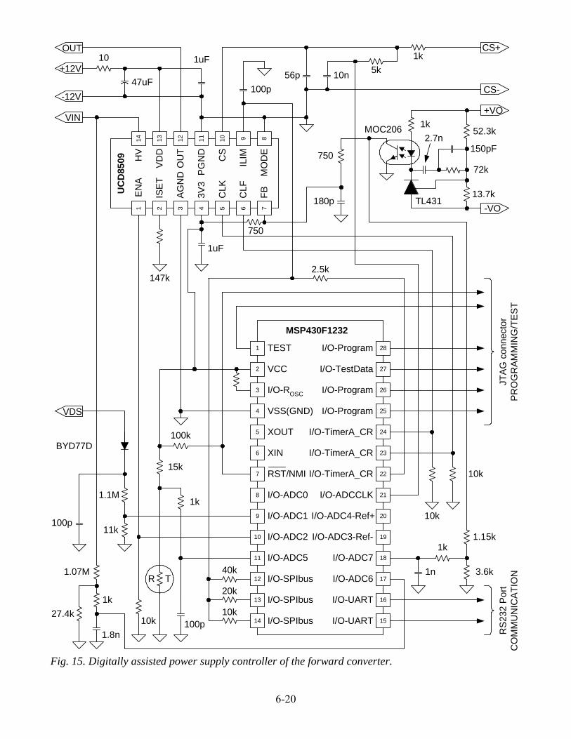
The schematic in Fig. 14 also indicates the different signal connections to the control circuit which is shown in Fig. 15.
CS+
+VIN
-VIN
+VOUT
-VOUT
10uH
82uF
1uF
0.1uF
2xMBR20100CT
7.5
7.5
1n
1n
50:1
7T 5T
5T
SUM65N20-30
VDS
OUT
VIN
+12V
CS-
-12V
GND
47uF2x
BAS21
470uH0.1uF
16V
47n 3 150
MBR0530
5
4uF
MBR0530
+VO
-VO
Fig. 14. 100-W resonant reset forward power stage.
6-20
9
21 43
1314 1112
6510
78
AG
ND P
GN
D
CS
ILIM
MO
DE
OU
T
VD
D
HV
FBCLF
CLK
3V3
ISE
T
EN
A
UC
D85
09
9
2
1
4
3
13
14
11
12
6
5
10
7
8
TEST
MSP430F1232
20
27
28
25
26
16
15
18
17
23
24
19
22
21
VCC
I/O-ROSC
VSS(GND)
XOUT
XIN
RST/NMI
I/O-ADC0
I/O-ADC1
I/O-ADC2
I/O-ADC5
I/O-SPIbus
I/O-SPIbus
I/O-SPIbus I/O-UART
I/O-UART
I/O-ADC6
I/O-ADC7
I/O-ADC3-Ref-
I/O-ADC4-Ref+
I/O-ADCCLK
I/O-TimerA_CR
I/O-TimerA_CR
I/O-TimerA_CR
I/O-Program
I/O-Program
I/O-TestData
I/O-Program
JTAG
con
nect
orPR
OG
RAM
MIN
G/T
EST
RS
232
Por
tC
OM
MU
NIC
ATI
ON
VIN
+12V
-12V
VDS
OUT CS+
CS-
TR
+VO
-VO
10
47uF
1uF 1k5k10n56p
10k
10k
1k
TL431
100k
10k
20k
40k
1uF
147k
750
1.15k
3.6k
1k
1n
100p
1k
15k
10k1.8n
1k
1.07M
27.4k
1.1M
11k100p
150pF
52.3k
13.7k
72k
2.7nMOC206
180p
750
100p
2.5k
BYD77D
Fig. 15. Digitally assisted power supply controller of the forward converter.

6-21
The controller operates with a fixed, 500kHz switching frequency and implements current mode control using the primary switch current information. The primary side control circuit is comprised of two ICs representing the demarcation between analog and digital control functions. The digital portion of the control algorithm is implemented in the MSP430F1232. The microcontroller is connected to the power stage and powered through the UCD8509 type analog controller which was specifically developed for digital power supply control applications in single ended converters. The regulation of the power supplys isolated output is performed by the opto isolated error amplifier section based on the popular TL431 integrated circuit.
C. Functional Description The division between analog and digital
control functions is based on the capabilities of the selected processor and the amount of computational resources needed to perform the control functions. In general, the more high speed control functions are moved to the digital domain, a higher performance, more expensive microcontroller or DSP is needed to execute the control algorithm. The most difficult functions for the digital controller are the voltage regulation loop, the digital pulse width modulation, the implementation of peak current mode control with slope compensation or input voltage feed forward in voltage mode control and over current protection. These functions correspond to fast changing signals which have to be measured and recalculated on the switching frequency basis or require immediate action to protect the power supply. The utilization of a dedicated analog building block can remove the burden of these computation intensive tasks from the processor and allow using a cost effective microcontroller. In addition, using analog circuits for the basic high speed power supply functions also permits the use of familiar analog control principles to ensure the stability of the power supply. The development of an analog controller also presents the opportunity to optimize the partitioning and the signal interface between the digital and analog portions of the controller.
Analog Functions – UCD8509 The UCD8509 is a highly integrated analog
companion chip to a microcontroller to implement digitally assisted power supply control. Its primary purpose is to provide high speed, analog pulse width modulation and secure over current protection. It also includes all auxiliary housekeeping function to service the microcontroller and a specialized interface to effectively communicate using only a few digital signals. The simplified block diagram is illustrated in Fig. 16.
ENA
ISET
AGND
3V3
CLK
CLF
FB
14 HV
VDD
OUT
PGND
CS
ILIM
MODE
PWM
CURRENTLIMIT
3.3VBIAS REG.
3.3V
START UPREG.
VDD
UVLO &BIAS OK
13
12
11
10
9
87
6
5
4
1
2
3
Fig. 16. UCD8509 simplified block diagram.
In telecom or similar input voltage applications, an on-board start up regulator provides initial bias to the chip which can be connected directly to the input power source. The start up regulators maximum input voltage is 110V. Once the power supply is up and running, the start up regulator turns off and the auxiliary power must be provided by a bootstrap power supply as shown in the schematic diagram in Fig. 14. The bootstrap voltage must be between 8V and 15V which is the recommended operating voltage range of the UCD8509.
The on-board 3.3V regulator draws power from the VDD rail and provides bias to the ICs internal circuits and to the microcontroller. The maximum external current consumption must be kept below 10mA, thus using a low power microcontroller is desirable.

6-22
The UCD8509 includes a high current output to drive the gate of an external power MOSFET. The gate driver switches between ground and the actual VDD voltage and has approximately 4A sink and 2.5A source current capability.
The controller also accommodates a high speed analog PWM section which can be set up for voltage or peak current mode operation according to the MODE input. The operating mode can be selected by shorting the pin to ground or to 3.3V, or by the microcontroller driving the MODE pin directly. While the UCD8509 has no oscillator, an internal local ramp generator is employed for the pulse width modulation in voltage mode. The same ramp generator is used to provide slope compensation in current mode. The slope of the ramp is adjusted by an external resistor connected to the ISET pin. The converters operating duty cycle is controlled by the error voltage which has to be connected to the FB pin.
One of the most important features of the UCD8509 is to provide instantaneous and
autonomous over current protection for the power stage without any help from the microcontroller. This function is implemented in the current limit block. For autonomous operation the UCD8509 has a default, internally set 0.5V current limit threshold which can be overridden by the microcontroller or by an external resistor network through the ILIM terminal. For added protection, the current limit adjustment range is internally limited between ground and twice the default value, i.e. between 0V and 1V. In case the cycle by cycle current limit circuit is activated, the UCD8509 will set the current limit flag (CLF) output high which can be read by the digital controller. The flag is automatically cleared before the beginning of the next switching period making it easy for the microcontroller to count the number of switching periods terminated by the current limit circuit.
The operating principle of the UCD8509 and the interaction between the microcontroller and the analog PWM block can be explained using the timing diagram in Fig. 17.
OUT
RAMP*
FB
CLF
CLK
ENA
UVLO &BIAS OK*
* - Internal signals
PWM*
Start up Steady State Current limit
Fig. 17. UCD8509 timing diagram (voltage mode operation).

6-23
During initial start up the UCD8509 establishes its own bias voltage (VDD) and the 3.3V bias for the microcontroller. During this time the CLF output is high, indicating for the digital circuit that the analog functions are not yet available. When all internal voltages are at their nominal level the CLF signal is cleared and the operation can commence. At that time the microcontroller is expected to enable the operation by setting the enable signal high and start sending the CLK pulse train.
The CLK signal carries two important pieces of information to supervise the operation of the UCD8509. As shown in Fig. 17, coinciding with the rising edge of CLK signal the pulse width modulator is reset and the gate drive output turns on indicating the beginning of the next switching period. Thus the switching frequency is determined by the rising edge of the waveform. The width of the CLK pulse limits the maximum on-time of the gate drive output. In fact, the duty ratio of the CLK signal is used as a variable maximum duty cycle clamp. According to the functions programmed in the microcontroller, the width of the CLK pulse is continuously recalculated by the digital controller and can be used to implement several control functions. Fig. 17 exemplifies how to use the CLK pulse width to implement soft-start.
During normal operation the converters duty ratio is less than the limit imposed by the digital controller, hence it is determined strictly by the analog PWM circuit of the UCD8509. Therefore the time domain resolution of the microcontroller is not a concern anymore. Assuming that the voltage regulation loop is also analog, as it is the case in the example power supply in Fig. 14 and 15, the small signal stability of the power supply can be ensured by obeying the familiar analog rules.
In current limit, the UCD8509s cycle-by-cycle current limit comparator overrides both duty cycle values the pulse width of the CLK input and the duty cycle of the analog pulse width modulator. The gate drive pulse terminates when the switch current reaches the current limit threshold. The threshold can be the default value or the adjusted voltage present at the ILIM pin. When the current limit circuit is activated the
CLF signal goes high for the remainder of the switching period and the information can be managed by the microcontroller according to its software.
An important feature of the current limit block is its complete independence from the signals of the digital controller. The current limit event is latched and kept in the memory of the UCD8509 until the next switching period is initiated by the microcontroller. This technique can protect the power stage in case the digital controller stalls. The CLK input can freeze in either state, the current limit circuit will protect the power stage and keep the power switch off until the pulse train is restored and the next rising edge of the CLK signal resets the current limit circuit.
Software Functionality Since the UCD8509s control functionality is
limited to pulse width modulation, peak current limiting and start up bias generation, all other control functions on the primary side of the power supply must be executed by the digital controller. Accordingly, the MSP430F1232 controls the following functions in the demonstration power supply: • Operating frequency • Input line UVLO • Input line OVP • Absolute duty cycle limit DMAX • Volt-second clamp DLIM(VIN) • Soft-start DLIM(tSS) • Current limit threshold adjustment • Current limit profile (delayed shutdown based
on the number of allowable events) • Temperature shutdown • MOSFET over voltage protection
In order to perform these functions the microcontroller needs to know the following variables: • fCLK its own clock frequency • fSW switching frequency • VIN,ON turn-on input voltage thresholds • VIN,OFF turn-off input voltage thresholds • DMAX maximum allowable duty ratio based
on the reset requirements of the transformer • DC transfer function to calculate
appropriate volt-second limit

6-24
• tSS duration of the soft-start interval • TMAX maximum board temperature • VDS,MAX highest acceptable drain-source
voltage These numbers can be entered through the
graphical user interface of the demonstration software and will be incorporated in the executable code of the microcontroller. The screen shot of the demonstration softwares user interface is pictured in Fig. 18.
In addition to the values entered by the user, the digital controller must measure and handle four more inputs: • VIN input line voltage • VDS drain to source voltage • TBOARD board temperature • CLF current limit flag
The demonstration hardware measures two additional parameters for future expansion of the software functionality. These are VFB and IIN,AVE, the feedback voltage and the average input current, respectively.
Fig. 18. Graphical user interface of the demonstration software.

6-25
Setting the Operating frequency The MSP430F1232 is set up with a core
clock frequency of 8MHz which frequency corresponds to the execution of the program instructions. The microcontroller can be tricked to operate its PWM timer at twice the clock frequency, which opportunity was utilized in this design. Based on fCLK=16MHz and fSW=500kHz, the switching period consists of:
32Hz10500Hz1016n 3
6
=⋅⋅=
clock cycle of the PWM timer. Accordingly, the minimum duty cycle adjustment can be calculated as:
ns562Hz1016
1t 6 .=⋅
=∆
or the duty cycle resolution is given as: 031250ns562Hz10500D 3 .. =⋅⋅=∆
Because the pulse width modulation is still done in analog by the UCD8509, the microcontrollers resolution impacts only the accuracy of the maximum duty ratio and the volt-second limit. For these functions the achieved resolution is sufficient.
Since the core of the microcontroller runs only with an 8 MHz clock frequency, every switching period contains 16 instruction cycles for program execution.
Maximum Duty Cycle The power stage design allows a maximum
operating duty ratio of approximately 80% to accommodate the reset time of the transformer. To provide some margin the controller is set up to limit the duty ratio at 75% or 24 clock cycles of the PWM timer (32·0.75=24).
Input Voltage Measurement Knowing the actual input voltage value
allows the digital controller to perform several housekeeping and protection functions. In this design the input voltage is measured by the on-board analog-to-digital converter. Since the ADC input is limited to the 0V 2.5V range by the reference of the analog-to-digital converter, the anticipated input voltage range must be scaled down to meet this constraint. Assuming 100V
maximum input voltage transient, the gain of the resistive divider can be calculated as:
0250V100V52GINPUT .. ==
This factor is implemented by the 1.07MΩ and 27.4kΩ resistors which are connected to the ADC6 input of the MSP430F1232 through an additional noise filter as shown in Fig. 15, the schematic diagram of the controller.
The ADC of the MSP430F1232 is a 10-bit analog-to-digital converter, therefore the 100V full scale input voltage range is represented by 210=1,024 individual values and the measurement resolution is:
mV982
V100res 10INPUT ≅=
As this number indicates it is really easy to accurately adjust the turn-on or turn-off input voltage levels of the power supply. The demonstration circuit uses the result of the input voltage measurement to provide software programmable line under and over voltage protection with user adjustable hysteresis and to implement an input voltage dependent duty ratio limit, also known as volt-second clamp. The V·s clamp is based on the DC transfer function of the power stage and can be calculated as:
INS
P
IN
OUTINLIM V
151821NN
VVVD ⋅≅⋅⋅= ..)(
where NP and NS are the primary and secondary number of turns of the transformer and the 1.1 multiplier indicates that the volt-second clamp is set 10% higher than the operating duty ratio of the converter. The working of the volt-second routine is demonstrated in Fig. 19 through 21.

6-26
CLK
OUT
VDS
ID
Fig. 19. Operating waveforms at VIN = 36 V.
CLK
OUT
VDS
ID
Fig. 20. Operating waveforms at VIN = 48 V.
CLK
OUT
VDS
ID
Fig. 21. Operating waveforms at VIN = 76 V.
The converters steady state operating duty ratio can be deciphered from the VDS waveform of the switching transistor. The maximum allowable duty ratio (DLIM(VIN)) is calculated by the microcontroller and it is based on the actual input voltage level. Its value is represented by the duty ratio of the CLK waveform. As the three figures demonstrate, the duty ratio of the CLK signal is approximately 10% higher than the operating duty cycle of the converter at all three input voltages.
Soft-Start The soft-start time of the converter can be
programmed through the software and will be implemented by the digital controller by gradually increasing the duty ratio of the converter. It is the same method outlined earlier in the Soft-Start Operation section under Miscellaneous Control Functions. The practical implementation starts by calculating the number of duty cycle values between zero duty cycle and DMAX.
24750Hz10500Hz1016D
ffSS 3
6
MAXSW
CLKSTEPS =⋅
⋅⋅=⋅= .
If the duty cycle limit would be increased by one step in every switching period the converter would reach maximum duty cycle in 24 switching period or in 60us. This is an unusually fast start up and it is also questionable whether the output capacitor can be charged to the nominal level within this time interval. To achieve a reasonable soft-start time in the milliseconds range, each of the 24 duty cycle values between zero and DMAX has to be maintained for several switching periods. For instance, if the soft-start time is given as tSS=5ms, each duty ratio must be valid for nSS number of switching cycles which can be obtained as:
104005024
Hz10500tSS
fn3
SSSTEPS
SWSS ≅⋅⋅=⋅= .
The effect of the gradually increasing discrete duty cycle values is demonstrated in Fig. 22. In order to show the step function in the output voltage waveform the soft-start time had to be extended to approximately 8 seconds.

6-27
VO
Fig. 22. Output voltage waveform with artificially long soft-start time.
VO
Fig. 23. Output voltage ramp up with 5ms soft-start time.
The normal 5ms long soft-start waveform of the converter is shown in Fig. 23 and it demonstrates the usual monotonic ramp up of the converters output voltage.
Current Limit Operation Using the capabilities of the UCD 8509, the
digital controller is able to adjust the current limit threshold and also the overload behavior of the power supply.
To override the default 0.5V current limit threshold of the analog current limit circuit, its ILIM pin voltage needs to be overridden. For current limit adjustment the UCD8509 expects an analog voltage at the ILIM terminal which can be generated by the microcontroller. Since the MSP430F1232 has no digital-to-analog converter on-board, the function is implemented by four of its digital I/O ports and an external resistor network as shown in Fig. 24.
13
14
12I/O-SPIbus
I/O-SPIbus
I/O-SPIbus10k
20k
40k
22I/O-TimerA_CR
ILIM
2.49k
1n
MSP430F1232 UCD8509
9
Fig. 24. Current limit adjustment using “poor man’s DAC”.
The digital output ports are three state outputs, they can be high impedance or connected either to GND or to the VCC voltage of the microcontroller. When all four outputs are high impedance, the default 0.5V threshold of the UCD8509 prevails. Assuming that pin 22 of the MSP430F1232 is connected to ground, to limit the maximum ILIM voltage below the 1V maximum threshold of the UCD8509, the microcontroller can select from 27 individual current limit thresholds between 0V and 1V using the other three ports.
During overload, the conduction time of the power MOSFET is limited by the cycle-by-cycle current limit circuit. When the current sense signal amplitude reaches the current limit threshold the gate drive output is immediately terminated to protect the power stage. This event is indicated by the CLF pin of the UCD8509 going high and can be read by the microcontroller. The typical waveforms of the converter in current limit mode are shown in Fig. 25.

6-28
CLK
OUT
VDS
CLF
Fig. 25. Current limit operation.
In this design the power supply is allowed to operate in current limit mode for a fixed number of switching cycles before it shuts down. The number of cycles in current limit mode before shut down can be entered by the user through the GUI of the demonstrations software. This operating mode allows short periods of overload conditions occurring typically during load transients without the need to increase the steady state current limit of the power supply.
Temperature Protection The demonstration power supply is equipped
with a temperature shut down feature based on the board temperature of the module. In order to get a better reading of the critical temperature of the power components, an external sensor is favored over the built-in temperature sensor of the microcontroller. The thermistor is placed in close proximity to the power MOSFET.
In order to eliminate any potential noise coupling, its signal is filtered near the input pin (pin 11 I/O-ADC5) of the MSP430F1232. The shut down threshold as well as the hysteresis of the temperature protection is user adjustable using the parameter entry screen of the demonstration software.
MOSFET Over Voltage Protection The last protection function of the converter
is based on the peak voltage stress of the primary MOSFET. The maximum voltage across the drain source terminal of the device is scaled and peak rectified. Once the measured stress voltage reaches the user entered shutdown threshold the converter stops operating. The shut down is followed by an automatic restart, initiating the full soft-start routine.
Software Algorithm Without going too deep into the fine details
of the software, one important characteristic of the controlling algorithm must be highlighted. In most applications the available computational resources and data conversion speed necessitates that the execution of the software functions are distributed over several switching periods. Accordingly, the functions are divided to two categories; basic functions which must be executed in every switching period and auxiliary routines which are scheduled over a longer period. This scheduling technique is demonstrated in Fig. 26.
Tim
ebas
e &
CLK
set
Sta
rt M
easu
re V
INTi
meb
ase
& C
LK s
et
Tim
ebas
e &
CLK
set
Tim
ebas
e &
CLK
set
Tim
ebas
e &
CLK
set
Tim
ebas
e &
CLK
set
Tim
ebas
e &
CLK
set
Rea
d V IN
Tim
ebas
e &
CLK
set
Tim
ebas
e &
CLK
set
Tim
ebas
e &
CLK
set
Star
t Mea
sure
VD
S
Rea
d V D
SS
tart
Mea
sure
VIN
Rea
d T B
OA
RD
Rea
d V IN
Sta
rt M
easu
re I IN
,AV
E
Che
ck U
VLO
& O
VP
Ser
vice
RS
-232
por
t
Ser
vice
RS
-232
por
t
Tim
ebas
e &
CLK
set
Tim
ebas
e &
CLK
set
Rea
d I IN
,AV
E
Tim
ebas
e &
CLK
set
Sta
rt M
easu
re V
INTi
meb
ase
& C
LK s
et
Upd
ate
Par
amet
ers
Upd
ate
Par
amet
ers
Che
ck U
VLO
& O
VP
Che
ck T
BO
AR
D li
mit
Che
ck V
DS li
mit
TSW
Upd
ate
DLI
M
Upd
ate
DLI
M
Fig. 26. Software scheduling example.

6-29
The diagram shows the program flow in steady state operation. The basic time base and CLK signal generation functions are performed in every switching cycle since they are essential to the proper operation of the analog companion circuit. In every third cycle the microcontroller initiates a signal measurement. The frequency of the ADC conversions is limited by the maximum speed of the analog-to-digital converter of the microcontroller. Since the most important input parameter is the input voltage, every second measurement cycle is dedicated to the input voltage measurement. In between the input voltage measurements the other analog parameters are measured in a rotating fashion. Once a measurement result is available, the microcontroller recalculates its internal variables and compares the measurement result against the limit values of the particular variable. In addition, a significant amount of the microcontrollers resources are reserved for communication in the demonstration software because of the frequent update of the displayed results.
Some of the software functions are assisted by specialized hardware resources in the MSP430F1232. For instance, no significant resources are allocated to handle the CLF signal. The number of current limit cycles is counted by the microcontrollers capture & compare register which generates an interrupt when the allowed number of consecutive current limit cycles is reached.
This short description of the software does not attempt to cover all aspects of the software development, but rather to show the level of expertise required to write the program. When power supply engineers make the first steps towards digital control, it might be wise to supplement their vast amount of power supply know-how with the proficiency of a skilled software engineer as it was the case in this project.
VI. SUMMARY This paper aimed to introduce digital power
supply control to the practicing power supply design community. Like most new technology, digital control in power supplies is expected to start its proliferation slowly. But this is definitely a trend not to overlook in the years to come.
At the same time, it is important to remember that the power supply is still a fundamentally analog circuit. The knowledge of various power supply topologies and related analog design expertise can not be substituted even by the most advanced software algorithm. On the other hand, digital implementation of the converters control offers new opportunities to develop advanced features and make the power supply a more visible, more integrated part of the system.
While transitioning to full digital control might require a completely different approach and skill set in the controller design, the circuit example of this paper presents a practical, intermediate step towards that final goal. As demonstrated by this converter, advanced features and protection functions, and communication capability can be integrated cost effectively and reliably in a quarter brick form factor.

IMPORTANT NOTICE
Texas Instruments Incorporated and its subsidiaries (TI) reserve the right to make corrections, modifications,enhancements, improvements, and other changes to its products and services at any time and to discontinueany product or service without notice. Customers should obtain the latest relevant information before placingorders and should verify that such information is current and complete. All products are sold subject to TI’s termsand conditions of sale supplied at the time of order acknowledgment.
TI warrants performance of its hardware products to the specifications applicable at the time of sale inaccordance with TI’s standard warranty. Testing and other quality control techniques are used to the extent TIdeems necessary to support this warranty. Except where mandated by government requirements, testing of allparameters of each product is not necessarily performed.
TI assumes no liability for applications assistance or customer product design. Customers are responsible fortheir products and applications using TI components. To minimize the risks associated with customer productsand applications, customers should provide adequate design and operating safeguards.
TI does not warrant or represent that any license, either express or implied, is granted under any TI patent right,copyright, mask work right, or other TI intellectual property right relating to any combination, machine, or processin which TI products or services are used. Information published by TI regarding third-party products or servicesdoes not constitute a license from TI to use such products or services or a warranty or endorsement thereof.Use of such information may require a license from a third party under the patents or other intellectual propertyof the third party, or a license from TI under the patents or other intellectual property of TI.
Reproduction of information in TI data books or data sheets is permissible only if reproduction is withoutalteration and is accompanied by all associated warranties, conditions, limitations, and notices. Reproductionof this information with alteration is an unfair and deceptive business practice. TI is not responsible or liable forsuch altered documentation.
Resale of TI products or services with statements different from or beyond the parameters stated by TI for thatproduct or service voids all express and any implied warranties for the associated TI product or service andis an unfair and deceptive business practice. TI is not responsible or liable for any such statements.
Following are URLs where you can obtain information on other Texas Instruments products and applicationsolutions:
Products Applications
Amplifiers amplifier.ti.com Audio www.ti.com/audio
Data Converters dataconverter.ti.com Automotive www.ti.com/automotive
DSP dsp.ti.com Broadband www.ti.com/broadband
Interface interface.ti.com Digital Control www.ti.com/digitalcontrol
Logic logic.ti.com Military www.ti.com/military
Power Mgmt power.ti.com Optical Networking www.ti.com/opticalnetwork
Microcontrollers microcontroller.ti.com Security www.ti.com/security
Telephony www.ti.com/telephony
Video & Imaging www.ti.com/video
Wireless www.ti.com/wireless
Mailing Address: Texas Instruments
Post Office Box 655303 Dallas, Texas 75265
Copyright 2005, Texas Instruments Incorporated