semiconducting polymers with nanocrystallites ...snml.kaist.ac.kr/jou_pdf/139.semiconducting...
TRANSCRIPT

Semiconducting Polymers with Nanocrystallites Interconnected viaBoron-Doped Carbon NanotubesKilho Yu,†,‡ Ju Min Lee,∥ Junghwan Kim,†,‡ Geunjin Kim,†,‡ Hongkyu Kang,†,‡ Byoungwook Park,†,‡
Yung Ho Kahng,§ Sooncheol Kwon,†,‡ Sangchul Lee,† Byoung Hun Lee,† Jehan Kim,⊥ Hyung Il Park,∥
Sang Ouk Kim,*,∥ and Kwanghee Lee*,†,‡,§
†Department of Nanobio Materials and Electronics, School of Materials Science and Engineering, ‡Heeger Center for AdvancedMaterials (HCAM), and §Research Institute for Solar and Sustainable Energies (RISE), Gwangju Institute of Science andTechnology (GIST), Gwangju 500-712, Republic of Korea∥Center for Nanomaterials and Chemical Reactions, Institute for Basic Science (IBS), Department of Materials Science andEngineering, Korea Advanced Institute of Science and Technology (KAIST), Daejeon 305-701, Republic of Korea
⊥Pohang Accelerator Laboratory (PAL), Pohang University of Science and Technology (POSTECH), Pohang 790-784,Republic of Korea
*S Supporting Information
ABSTRACT: Organic semiconductors are key building blocksfor future electronic devices that require unprecedented prop-erties of low-weight, flexibility, and portability. However, thelow charge-carrier mobility and undesirable processing con-ditions limit their compatibility with low-cost, flexible, andprintable electronics. Here, we present significantly enhancedfield-effect mobility (μFET) in semiconducting polymers mixedwith boron-doped carbon nanotubes (B-CNTs). In contrast toundoped CNTs, which tend to form undesired aggregates, theB-CNTs exhibit an excellent dispersion in conjugated polymermatrices and improve the charge transport between polymerchains. Consequently, the B-CNT-mixed semiconducting polymers enable the fabrication of high-performance FETs on plasticsubstrates via a solution process; the μFET of the resulting FETs reaches 7.2 cm
2 V−1 s−1, which is the highest value reported for aflexible FET based on a semiconducting polymer. Our approach is applicable to various semiconducting polymers without anyadditional undesirable processing treatments, indicating its versatility, universality, and potential for high-performance printableelectronics.
KEYWORDS: Semiconducting polymer, carbon nanotube, polymer nanocrystallite, nanocomposite, field-effect transistor,room-temperature process
Organic field-effect transistors (OFETs) based on semi-conducting polymers have been intensively investigated
for future ubiquitous devices in which unprecedented devicefeatures such as low-weight, flexibility, and portability are re-quired.1−4 Moreover, the solution processability of the semi-conducting polymers enables the cost-effective, large-scalefabrication of OFETs on plastic substrates via high-throughputprinting technologies.5−7 Nevertheless, their poor charge-carriermobility (μ) has hindered the realization of their potentialadvantages.8 Because of remarkable advances in the develop-ment of processing techniques, the state of the art of solution-processed semiconducting polymers recently reached a remark-able stage9 of μ ∼ 36 cm2 V−1 s−1. However, because thesetechniques still require undesirable processing treatments, suchas thermal annealing at high temperature (T)10,11 (typically, T ≥200 °C) and/or macroscopic alignment processes9,12−15 usingmechanically grooved inorganic substrates, they are not com-patible with the concept of “flexible and printable electronics”
using plastic substrates. Fabricating high-μ semiconducting poly-mer layers on plastic substrates from a solution process at room-temperature (RT) has been a formidable challenge.One promising approach involves introducing carbon nano-
tubes (CNTs) into semiconducting polymers.16 CNTs possessall the outstanding properties as a μ-enhancer in OFETs,including a high-μ, good mechanical flexibility, and a high aspectratio.17 CNTs in semiconducting polymers act as ballisticconduction bridges18 between the polymer chains and/or inducea local alignment of the polymer chains located in the vicinity ofCNTs,19,20 thereby significantly improving the μ value of thepolymers. However, because CNTs tend to easily aggregate viavan der Waals interaction,21,22 most CNT-based OFETs havesuffered from poor device performance and electrical break-down.23 Although many different solutions for overcoming this
Received: September 17, 2014Published: November 5, 2014
Letter
pubs.acs.org/NanoLett
© 2014 American Chemical Society 7100 dx.doi.org/10.1021/nl503574h | Nano Lett. 2014, 14, 7100−7106
aggregation problem have been explored including surfacefunctionalization24−26 and in situ polymerization,27−29 theseefforts have thus far failed to satisfy the requirements for high-performance flexible FETs.In this work, we report for the first time significantly enhanced
field-effect μ in conjugated polymers mixed with a small amountof boron-doped CNTs (B-CNTs). In contrast to undopedCNTs (U-CNTs), which tend to form undesired aggregates, theB-CNTs exhibit excellent dispersion in a conjugated polymermatrix. The substitutional doping of B atoms also effectivelyincreases the work function of CNTs and facilitates hole-transport between the semiconducting polymers and CNTs.More importantly, the well-dispersed CNTs on the molecularscale induce a local crystallization of the polymer chains even atRT, enabling the fabrication of high performance flexible OFETswith a top-gate geometry. The field-effect μ of our devices, whichwere fabricated on plastic substrates via a solution process at RT,reaches 7.2 cm2 V−1 s−1, which has never been previouslyachieved in a flexible FET based on a semiconducting polymer.The B-CNTs were processed using commercially available
multiwalled CNTs with an average length of ∼1 μm and adiameter of 10−15 nm. After the CNTs were purified, B-dopingwas performed via thermal treatment under an Ar/NH3 gasstream with vaporized B2O3 powder,
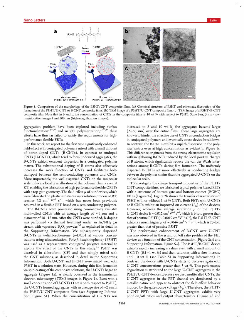
30 as explained in detail inthe Supporting Information. We subsequently dispersedB-CNTs in o-dichlorobenzene (o-DCB) at various concen-trations using ultrasonication. Poly(3-hexylthiophene) (P3HT)was used as a representative conjugated polymer material toexplore the effect of the CNTs in this study.31 P3HT wasdissolved in chloroform (CF) and then simply mixed withthe CNT solutions, as described in detail in the SupportingInformation. Both U-CNT and B-CNT were mixed well withP3HT in a solution state. However, during thin-film formationvia spin-casting of the composite solutions, the U-CNTs began toaggregate (Figure 1a), as clearly observed in the transmissionelectron microscopy (TEM) images in Figure 1b. Even with asmall concentration of U-CNTs (1 wt % with respect to P3HT),the U-CNTs formed aggregates with an average size of∼2 μm inthe P3HT/U-CNT composite films (see Supporting Informa-tion, Figure S1). When the concentration of U-CNTs was
increased to 5 and 10 wt %, the aggregates became larger(2−50 μm) over the entire films. These large aggregates areknown to hinder the effective use of CNTs as conduction bridgesin conjugated polymers and eventually cause device breakdown.In contrast, the B-CNTs exhibit a superb dispersion in the poly-mer matrix even at high concentration as evident in Figure 1c.This difference originates from the strong electrostatic repulsionwith neighboring B-CNTs induced by the local positive chargesof B atoms, which significantly reduce the van der Waals inter-actions among B-CNTs during film formation. The uniformlydispersed B-CNTs act more effectively as conducting bridgesbetween the polymer chains than the aggregated U-CNTs on themolecular scale.To investigate the charge transport properties of the P3HT/
CNT composite films, we fabricated typical polymer-based FETswith a structure of bottom-gate and bottom-contact (BGBC)FETs (Figure 2a). Figure 2b shows the transfer characteristics ofP3HT with or without 1 wt % CNTs. Both FETs with U-CNTsor B-CNTs exhibit an improved on-current (Ids) of the devices.However, whereas the average saturation μ of the P3HT/U-CNT device is∼0.012 cm2 V−1 s−1, which is 6-fold greater thanthat of pristine P3HT (∼0.0019 cm2 V−1 s−1), the P3HT/B-CNTexhibits a much higher μ of ∼0.044 cm2 V−1 s−1, which is 23-foldgreater than that of pristine P3HT.The performance enhancement of B-CNT over U-CNT
was also observed in the μ and on/off ratio profiles of the FETdevices as a function of the CNT concentration (Figure 2c,d andSupporting Information, Figure S2). The P3HT/B-CNT deviceexhibits rapidly increasing μ values even with a small amount ofB-CNTs (0.1−1 wt %) and then saturates with a slow increaseuntil 10 wt % (see Table S1 in Supporting Information). Incontrast, the device with U-CNTs starts to decrease again withU-CNT concentrations greater than 5 wt %. This performancedegradation is attributed to the large U-CNT aggregates in theP3HT/U-CNT devices. Because we used multiwalled CNTs, theU-CNT aggregates in the FET channel are dominated by ametallic nature and appear to obstruct the field-effect behaviorinduced by the gate-source voltage (Vgs). Therefore, the P3HT/U-CNT FETs with large U-CNT aggregates exhibit verypoor on/off ratios and output characteristics (Figure 2d and
Figure 1. Comparison of the morphology of the P3HT/CNT composite films. (a) Chemical structure of P3HT and schematic illustration of theformation of the P3HT/U-CNT or B-CNT composite films. (b) TEM image of a P3HT/U-CNT composite film. (c) TEM image of a P3HT/B-CNTcomposite film. Note that in b and c, the concentration of CNTs in the composite films is 10 wt % with respect to P3HT. Scale bars, 5 μm (low-magnification images) and 500 nm (high-magnification images).
Nano Letters Letter
dx.doi.org/10.1021/nl503574h | Nano Lett. 2014, 14, 7100−71067101
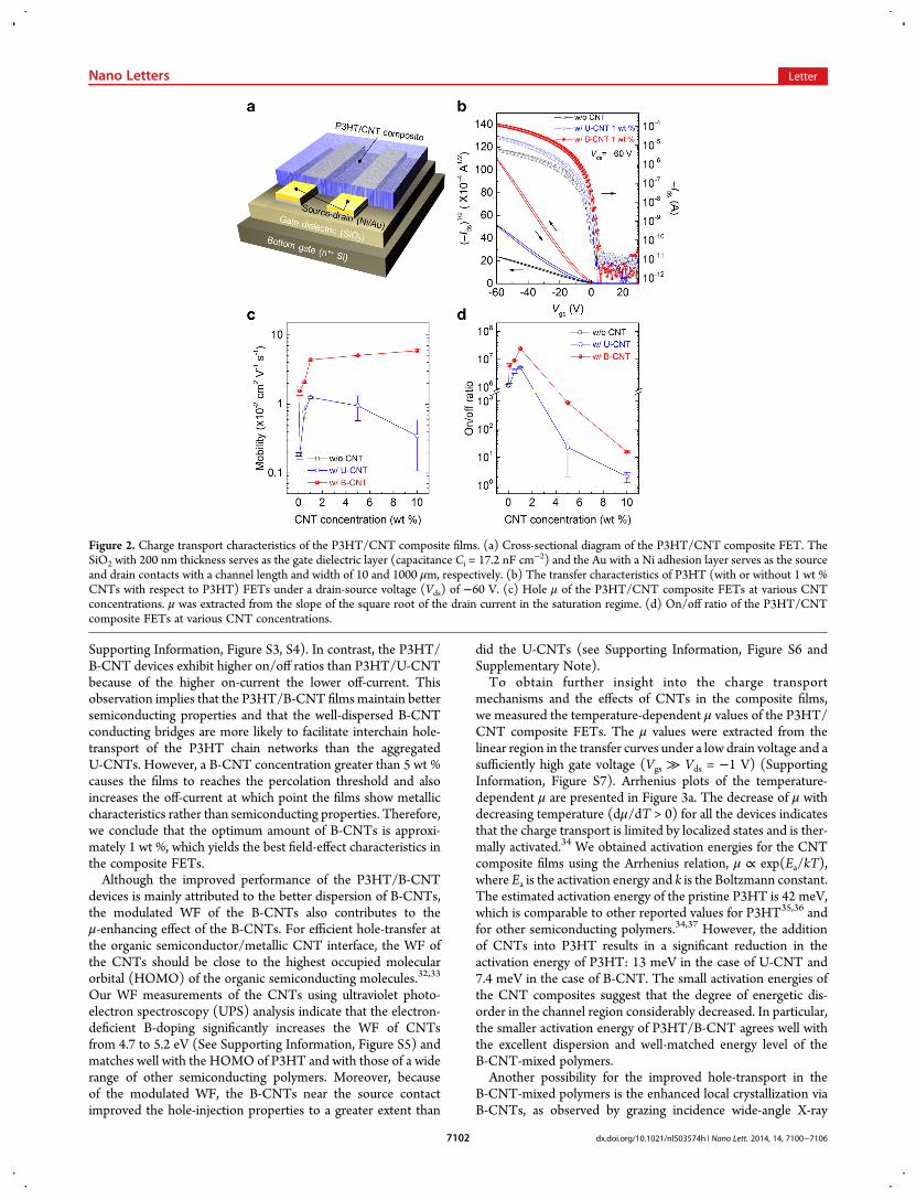
Supporting Information, Figure S3, S4). In contrast, the P3HT/B-CNT devices exhibit higher on/off ratios than P3HT/U-CNTbecause of the higher on-current the lower off-current. Thisobservation implies that the P3HT/B-CNT films maintain bettersemiconducting properties and that the well-dispersed B-CNTconducting bridges are more likely to facilitate interchain hole-transport of the P3HT chain networks than the aggregatedU-CNTs. However, a B-CNT concentration greater than 5 wt %causes the films to reaches the percolation threshold and alsoincreases the off-current at which point the films show metalliccharacteristics rather than semiconducting properties. Therefore,we conclude that the optimum amount of B-CNTs is approxi-mately 1 wt %, which yields the best field-effect characteristics inthe composite FETs.Although the improved performance of the P3HT/B-CNT
devices is mainly attributed to the better dispersion of B-CNTs,the modulated WF of the B-CNTs also contributes to theμ-enhancing effect of the B-CNTs. For efficient hole-transfer atthe organic semiconductor/metallic CNT interface, the WF ofthe CNTs should be close to the highest occupied molecularorbital (HOMO) of the organic semiconducting molecules.32,33
Our WF measurements of the CNTs using ultraviolet photo-electron spectroscopy (UPS) analysis indicate that the electron-deficient B-doping significantly increases the WF of CNTsfrom 4.7 to 5.2 eV (See Supporting Information, Figure S5) andmatches well with the HOMO of P3HT and with those of a widerange of other semiconducting polymers. Moreover, becauseof the modulated WF, the B-CNTs near the source contactimproved the hole-injection properties to a greater extent than
did the U-CNTs (see Supporting Information, Figure S6 andSupplementary Note).To obtain further insight into the charge transport
mechanisms and the effects of CNTs in the composite films,we measured the temperature-dependent μ values of the P3HT/CNT composite FETs. The μ values were extracted from thelinear region in the transfer curves under a low drain voltage and asufficiently high gate voltage (Vgs ≫ Vds = −1 V) (SupportingInformation, Figure S7). Arrhenius plots of the temperature-dependent μ are presented in Figure 3a. The decrease of μ withdecreasing temperature (dμ/dT > 0) for all the devices indicatesthat the charge transport is limited by localized states and is ther-mally activated.34 We obtained activation energies for the CNTcomposite films using the Arrhenius relation, μ ∝ exp(Ea/kT),where Ea is the activation energy and k is the Boltzmann constant.The estimated activation energy of the pristine P3HT is 42 meV,which is comparable to other reported values for P3HT35,36 andfor other semiconducting polymers.34,37 However, the additionof CNTs into P3HT results in a significant reduction in theactivation energy of P3HT: 13 meV in the case of U-CNT and7.4 meV in the case of B-CNT. The small activation energies ofthe CNT composites suggest that the degree of energetic dis-order in the channel region considerably decreased. In particular,the smaller activation energy of P3HT/B-CNT agrees well withthe excellent dispersion and well-matched energy level of theB-CNT-mixed polymers.Another possibility for the improved hole-transport in the
B-CNT-mixed polymers is the enhanced local crystallization viaB-CNTs, as observed by grazing incidence wide-angle X-ray
Figure 2. Charge transport characteristics of the P3HT/CNT composite films. (a) Cross-sectional diagram of the P3HT/CNT composite FET. TheSiO2 with 200 nm thickness serves as the gate dielectric layer (capacitance Ci = 17.2 nF cm−2) and the Au with a Ni adhesion layer serves as the sourceand drain contacts with a channel length and width of 10 and 1000 μm, respectively. (b) The transfer characteristics of P3HT (with or without 1 wt %CNTs with respect to P3HT) FETs under a drain-source voltage (Vds) of −60 V. (c) Hole μ of the P3HT/CNT composite FETs at various CNTconcentrations. μ was extracted from the slope of the square root of the drain current in the saturation regime. (d) On/off ratio of the P3HT/CNTcomposite FETs at various CNT concentrations.
Nano Letters Letter
dx.doi.org/10.1021/nl503574h | Nano Lett. 2014, 14, 7100−71067102

scattering (GIWAXS) measurements of the P3HT/CNTcomposite films. Figure 3b,c presents two-dimensional (2D)GIWAXS patterns of the P3HT and P3HT/CNT compositefilms, respectively. In the 2D patterns, two distinctive types ofpatterns are observed: one for (h00) peaks with a lamellarspacing ∼16.4 Å along the out-of-plane direction and the otherfor (010) peaks with a π−π spacing of∼3.73 Å along the in-planedirection. To evaluate the relationship between the structuralcharacteristics and the charge transport properties, we analyzedthe in-plane (010) peaks using 1D profiles, as shown in Figure 3d.We subsequently estimated the average crystallite size on thebasis of Scherrer’s equation using the full-width at half-maximum(fwhm) of the (010) peaks (Figure 3e). We observed that theaverage crystallite size substantially increased with an increase inthe amount of B-CNTs (0.1−1 wt %). We believe that theincreased crystallite size also contributes to the enhanced hole-μ,even when very few B-CNT bridges are present in the composite
films. However, in the case of B-CNT concentrations greaterthan 5 wt %, the average crystallite size again decreases. More-over, the evolution of the (100) peak in the in-plane profile of afilm with a B-CNT concentration greater than 5 wt % indicatesthat the crystal orientation is more randomly distributed witha larger amount of B-CNTs, as also observed in the azimuthalprofiles for the (100) peaks (Supporting Information, Figure S8).These results are consistent with the aforementioned field-effectcharacteristics. In contrast to the addition of B-CNTs, the addi-tion of U-CNTs did not greatly affect the polymer morphology.This observation implies that the aggregated U-CNTs rarelyinteract with polymer chains on the molecular scale. We demon-strated that a simple mixing of B-CNTs induces crystallization insemiconducting polymers and improves charge transport.To take full advantage of B-CNTs, we fabricated flexible FETs
based on RT-processed conjugated polymer/B-CNT compositesdirectly on commercially available poly(ethylene-2, 6-naphthalate)
Figure 3.Temperature-dependence and structural characteristics of P3HT/CNT composite FETs. (a) Temperature-dependence of the field-effect μ ofP3HT/CNT composite FETs. The μ values are estimated in the linear regime under a small Vds of−1 V. The straight lines represent the best Arrheniusfitting, and the slopes were used to extract the activation energies. The channel length and width of the devices are 50 and 1000 μm, respectively. (b,c)Normalized 2D GIWAXS patterns of (b) P3HT and (c) P3HT/CNT composite films with various CNT concentrations. (d) Normalized 1D profilesalong the in-plane direction obtained from the 2D GIWAXS profiles. (e) Average crystallite size of P3HT with various CNT concentrations.
Nano Letters Letter
dx.doi.org/10.1021/nl503574h | Nano Lett. 2014, 14, 7100−71067103
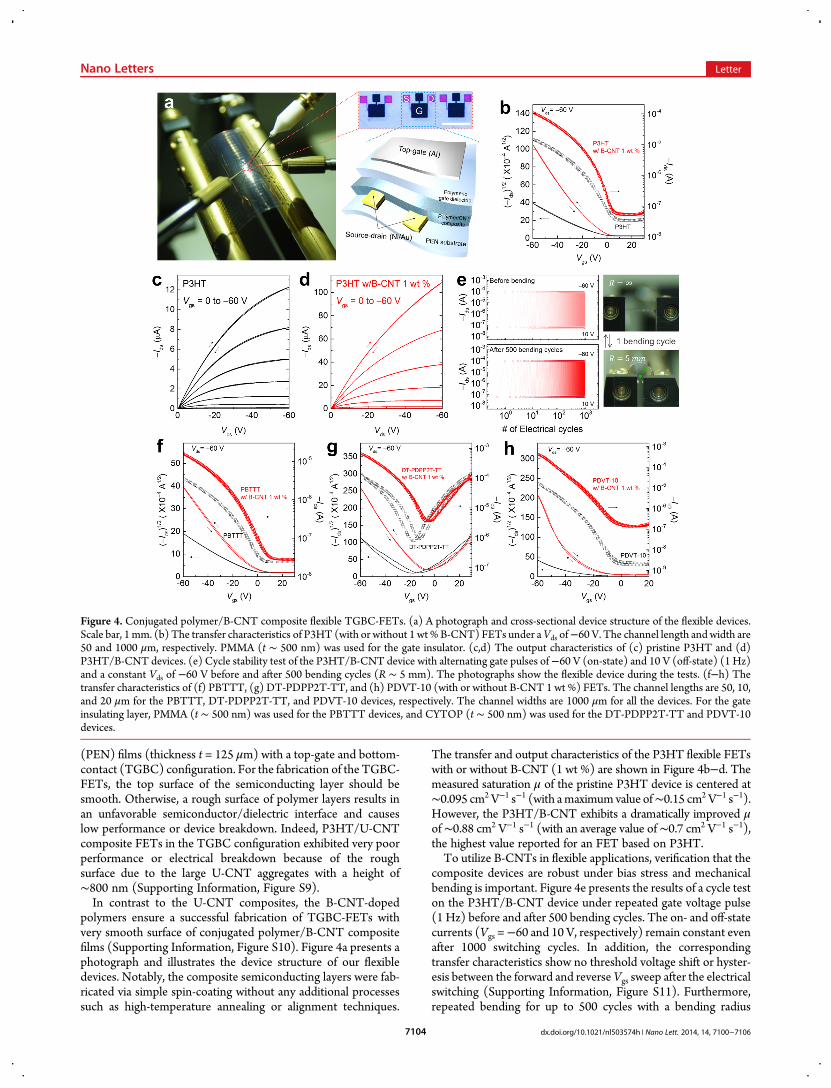
(PEN) films (thickness t = 125 μm) with a top-gate and bottom-contact (TGBC) configuration. For the fabrication of the TGBC-FETs, the top surface of the semiconducting layer should besmooth. Otherwise, a rough surface of polymer layers results inan unfavorable semiconductor/dielectric interface and causeslow performance or device breakdown. Indeed, P3HT/U-CNTcomposite FETs in the TGBC configuration exhibited very poorperformance or electrical breakdown because of the roughsurface due to the large U-CNT aggregates with a height of∼800 nm (Supporting Information, Figure S9).In contrast to the U-CNT composites, the B-CNT-doped
polymers ensure a successful fabrication of TGBC-FETs withvery smooth surface of conjugated polymer/B-CNT compositefilms (Supporting Information, Figure S10). Figure 4a presents aphotograph and illustrates the device structure of our flexibledevices. Notably, the composite semiconducting layers were fab-ricated via simple spin-coating without any additional processessuch as high-temperature annealing or alignment techniques.
The transfer and output characteristics of the P3HT flexible FETswith or without B-CNT (1 wt %) are shown in Figure 4b−d. Themeasured saturation μ of the pristine P3HT device is centered at∼0.095 cm2 V−1 s−1 (with amaximumvalue of∼0.15 cm2 V−1 s−1).However, the P3HT/B-CNT exhibits a dramatically improved μof∼0.88 cm2 V−1 s−1 (with an average value of∼0.7 cm2 V−1 s−1),the highest value reported for an FET based on P3HT.To utilize B-CNTs in flexible applications, verification that the
composite devices are robust under bias stress and mechanicalbending is important. Figure 4e presents the results of a cycle teston the P3HT/B-CNT device under repeated gate voltage pulse(1 Hz) before and after 500 bending cycles. The on- and off-statecurrents (Vgs =−60 and 10 V, respectively) remain constant evenafter 1000 switching cycles. In addition, the correspondingtransfer characteristics show no threshold voltage shift or hyster-esis between the forward and reverseVgs sweep after the electricalswitching (Supporting Information, Figure S11). Furthermore,repeated bending for up to 500 cycles with a bending radius
Figure 4. Conjugated polymer/B-CNT composite flexible TGBC-FETs. (a) A photograph and cross-sectional device structure of the flexible devices.Scale bar, 1mm. (b) The transfer characteristics of P3HT (with or without 1 wt% B-CNT) FETs under aVds of−60 V. The channel length andwidth are50 and 1000 μm, respectively. PMMA (t ∼ 500 nm) was used for the gate insulator. (c,d) The output characteristics of (c) pristine P3HT and (d)P3HT/B-CNT devices. (e) Cycle stability test of the P3HT/B-CNT device with alternating gate pulses of−60 V (on-state) and 10 V (off-state) (1 Hz)and a constant Vds of −60 V before and after 500 bending cycles (R ∼ 5 mm). The photographs show the flexible device during the tests. (f−h) Thetransfer characteristics of (f) PBTTT, (g) DT-PDPP2T-TT, and (h) PDVT-10 (with or without B-CNT 1 wt %) FETs. The channel lengths are 50, 10,and 20 μm for the PBTTT, DT-PDPP2T-TT, and PDVT-10 devices, respectively. The channel widths are 1000 μm for all the devices. For the gateinsulating layer, PMMA (t ∼ 500 nm) was used for the PBTTT devices, and CYTOP (t ∼ 500 nm) was used for the DT-PDPP2T-TT and PDVT-10devices.
Nano Letters Letter
dx.doi.org/10.1021/nl503574h | Nano Lett. 2014, 14, 7100−71067104

R∼ 5 mm did not result in any change in the electrical propertiesof the device.To verify the universal applicability of our B-CNT technique,
we also investigated flexible FETs using other conjugatedpolymers: poly(2,5-bis(3-dodecylthiophen-2-yl)thieno[3,2-b]-thiophene) (PBTTT),38 diketopyrrolopyrrole-based polymer(DT-PDPP2T-TT),11 and poly[2,5-bis(2-decyltetradecyl)-pyrrolo[3,4-c]pyrrole-1,4(2H,5H)-dione-alt-5,5′-di(thiophen-2-yl)-2,2′-(E)-2-(2-(thiophen-2-yl)vinyl)thiophene] (PDVT-10)10(their molecular structures are shown in Supporting Information,Figure S12). Figure 4f−h shows the transfer characteristicsof the flexible devices based on PBTTT, DT-PDPP2T-TT, andPDVT-10 with or without 1 wt % B-CNTs, respectively; theoutput characteristics of the corresponding devices are shown inSupporting Information, Figure S13. The liquid crystallinepolymer PBTTT (without heat treatment) exhibited a rather lowμ of ∼0.015 cm2 V−1 s−1 (with a maximum value of ∼0.022 cm2
V−1 s−1). However, after the addition of B-CNTs (1 wt %), thedevices exhibit a substantially improved μ of ∼0.090 cm2 V−1 s−1
(with a maximum value of ∼0.12 cm2 V−1 s−1). A similar effectwas also observed in the DT-PDPP2T-TT devices; withB-CNTs, a high μ of ∼1.7 cm2 V−1 s−1 (with a maximumvalue of ∼2.3 cm2 V−1 s−1) was achieved, whereas the pristinedevices exhibited an average μ of ∼0.40 cm2 V−1 s−1 (with amaximum value of ∼0.60 cm2 V−1 s−1). Notably, the highesthole-μ reported for this polymer is ∼0.80 cm2 V−1 s−1 in the caseof a high-temperature annealing process conducted at 200 °C.Finally, we fabricated PVDT-10 based devices. PDVT-10 has
also been reported to require high-temperature processing(∼180 °C) to induce structural ordering and a high charge-carrier μ. Our pristine PDVT-10 devices processed at RTexhibited an average hole-μ of 0.24 cm2 V−1 s−1 (with a maximumvalue of ∼0.31 cm2 V−1 s−1). However, the B-CNT-mixedPDVT-10 exhibited a significantly increased μ of ∼5.0 cm2 V−1
s−1 (with a maximum value of ∼7.2 cm2 V−1 s−1), which is morethan 20 times greater than that of the pristine devices. To the bestof our knowledge, this field-effect mobility value is the highestsuch value reported for a flexible polymer FET fabricated usinga plastic substrate and is even comparable to that of indium-gallium-zinc oxide (IGZO) FETs fabricated on flexible sub-strates.39−41
In summary, B-CNTs exhibit superior dispersion in polymermatrices even at high concentrations, whereas U-CNTs tend toform undesired aggregates. Therefore, using the conjugatedpolymers mixed with 1 wt % B-CNTs, we achieved a hole-μ of7.2 cm2 V−1 s−1 in FET devices fabricated on plastic substrates atRT. This value is the highest value reported for a polymer-basedflexible FET to date. Our results also indicate that the B-CNTtechnique is universal and works well with various semicon-ducting polymers without any additional undesirable process-ing treatments for future low-cost and printable electronicsapplications.
■ ASSOCIATED CONTENT*S Supporting InformationDetailed experimental procedures; additional results from FET,TEM, and GIWAXS characterizations; UPS spectra of CNTs;optical microscopy images of P3HT/CNT composite films;molecular structures of semiconducting polymers used for theflexible devices; and detailed discussion about charge-injection atsource contacts and transport properties of P3HT/CNTcomposites in FETs. This material is available free of chargevia the Internet at http://pubs.acs.org.
■ AUTHOR INFORMATION
Corresponding Authors*E-mail: (K.L.) [email protected] .*E-mail: (S.O.K.) [email protected].
NotesThe authors declare no competing financial interest.
■ ACKNOWLEDGMENTS
We thank the Heeger Center for Advanced Materials (HCAM)and the Research Institute of Solar & Sustainable Energies(RISE) at the Gwangju Institute of Science and Technology(GIST) of Korea for assistance with the device fabrication andcharacterization. K.L. also acknowledges support from aNationalResearch Foundation of Korea (NRF) grant funded by theKorean government (MSIP) (NRF-2014R1A2A1A09006137and No. 2008-0062606, CELA-NCRC). S.O.K. acknowledgessupport from IBS-R004-G1-2014-a00.
■ REFERENCES(1) Forrest, S. R. Nature 2004, 428, 911−918.(2) Rogers, J. A.; Someya, T.; Huang, Y. Science 2010, 327, 1603−1607.(3) Kaltenbrunner, M.; Sekitani, T.; Reeder, J.; Yokota, T.; Kuribara,K.; Tokuhara, T.; Drack, M.; Schwodiauer, R.; Graz, I.; Bauer-Gogonea,S.; Bauer, S.; Someya, T. Nature 2013, 499, 458−463.(4) Di, C.-a.; Zhang, F.; Zhu, D. Adv. Mater. 2013, 25, 313−330.(5) Zhao, Y.; Di, C.-a.; Gao, X.; Hu, Y.; Guo, Y.; Zhang, L.; Liu, Y.;Wang, J.; Hu, W.; Zhu, D. Adv. Mater. 2011, 23, 2448−2453.(6) Søndergaard, R. R.; Hosel, M.; Krebs, F. C. J. Polym. Sci., Part B:Polym. Phys. 2013, 51, 16−34.(7) Jung, M.; Kim, J.; Noh, J.; Lim, N.; Lim, C.; Lee, G.; Kim, J.; Kang,H.; Jung, K.; Leonard, A. D.; Tour, J. M.; Cho, G. IEEE Trans. ElectronDevices 2010, 57, 571−580.(8) Noriega, R.; Rivnay, J.; Vandewal, K.; Koch, F. P. V.; Stingelin, N.;Smith, P.; Toney, M. F.; Salleo, A. Nat. Mater. 2013, 12, 1038−1044.(9) Luo, C.; Kyaw, A. K. K.; Perez, L. A.; Patel, S.; Wang, M.; Grimm,B.; Bazan, G. C.; Kramer, E. J.; Heeger, A. J. Nano Lett. 2014, 14, 2764−2771.(10) Chen, H.; Guo, Y.; Yu, G.; Zhao, Y.; Zhang, J.; Gao, D.; Liu, H.;Liu, Y. Adv. Mater. 2012, 24, 4618−4622.(11) Li, W.; Hendriks, K. H.; Roelofs, W. S. C.; Kim, Y.; Wienk, M. M.;Janssen, R. A. J. Adv. Mater. 2013, 25, 3182−3186.(12) van de Craats, A. M.; Stutzmann, N.; Bunk, O.; Nielsen, M. M.;Watson, M.; Mullen, K.; Chanzy, H. D.; Sirringhaus, H.; Friend, R. H.Adv. Mater. 2003, 15, 495−499.(13) Tseng, H. R.; Ying, L.; Hsu, B. B. Y.; Perez, L. A.; Takacs, C. J.;Bazan, G. C.; Heeger, A. J. Nano Lett. 2012, 12, 6353−6357.(14) Hsu, B. B. Y.; Seifter, J.; Takacs, C. J.; Zhong, C.; Tseng, H.-R.;Samuel, I. D. W.; Namdas, E. B.; Bazan, G. C.; Huang, F.; Cao, Y.;Heeger, A. J. ACS Nano 2013, 7, 2344−2351.(15) Tseng, H.-R.; Phan, H.; Luo, C.; Wang, M.; Perez, L. A.; Patel, S.N.; Ying, L.; Kramer, E. J.; Nguyen, T.-Q.; Bazan, G. C.; Heeger, A. J.Adv. Mater. 2014, 26, 2993−2998.(16) Spitalsky, Z.; Tasis, D.; Papagelis, K.; Galiotis, C. Prog. Polym. Sci.2010, 35, 357−401.(17) Maiti, U. N.; Lee, W. J.; Lee, J. M.; Oh, Y.; Kim, J. Y.; Kim, J. E.;Shim, J.; Han, T. H.; Kim, S. O. Adv. Mater. 2014, 26, 40−67.(18) Li, H. J.; Lu, W. G.; Li, J. J.; Bai, X. D.; Gu, C. Z. Phys. Rev. Lett.2005, 95, 086601.(19) Alig, I.; Lellinger, D.; Dudkin, S. M.; Potschke, P. Polymer 2007,48, 1020−1029.(20) Lu, K.; Grossiord, N.; Koning, C. E.; Miltner, H. E.; Mele, B. v.;Loos, J. Macromolecules 2008, 41, 8081−8085.(21) Wijewardane, S. Sol. Energy 2009, 83, 1379−1389.(22) Ma, P.-C.; Siddiqui, N. A.; Marom, G.; Kim, J.-K. Composites, PartA 2010, 41, 1345−1367.
Nano Letters Letter
dx.doi.org/10.1021/nl503574h | Nano Lett. 2014, 14, 7100−71067105
(23) Park, Y. D.; Lim, J. A.; Jang, Y.; Hwang, M.; Lee, H. S.; Lee, D. H.;Lee, H.-J.; Baek, J.-B.; Cho, K. Org. Electron. 2008, 9, 317−322.(24) Chang, C. H.; Chien, C. H. IEEE Electron Device Lett. 2011, 32,1457−1459.(25) Park, S.; Jin, S.; Jun, G.; Jeon, S.; Hong, S. Nano Res. 2011, 4,1129−1135.(26) Jun, G. H.; Jin, S. H.; Park, S. H.; Jeon, S.; Hong, S. H. Carbon2012, 50, 40−46.(27) Park, S. J.; Cho, M. S.; Lim, S. T.; Choi, H. J.; Jhon, M. S.Macromol. Rapid Commun. 2003, 24, 1070−1073.(28) Song, Y. J.; Lee, J. U.; Jo, W. H. Carbon 2010, 48, 389−395.(29) Bai, X.; Hu, X.; Zhou, S.; Yan, J.; Sun, C.; Chen, P.; Li, L.Electrochim. Acta 2013, 87, 394−400.(30) Lee, J. M.; Park, J. S.; Lee, S. H.; Kim, H.; Yoo, S.; Kim, S. O. Adv.Mater. 2011, 23, 629−633.(31) Bao, Z.; Dodabalapur, A.; Lovinger, A. J. Appl. Phys. Lett. 1996, 69,4108−4110.(32) Ishii, H.; Sugiyama, K.; Ito, E.; Seki, K. Adv. Mater. 1999, 11, 605−625.(33) Braun, S.; Salaneck, W. R.; Fahlman, M. Adv. Mater. 2009, 21,1450−1472.(34) Salleo, A.; Chen, T. W.; Volkel, A. R.; Wu, Y.; Liu, P.; Ong, B. S.;Street, R. A. Phys. Rev. B 2004, 70, 115311.(35) Kline, R. J.; McGehee, M. D.; Kadnikova, E. N.; Liu, J.; Frechet, J.M. J.; Toney, M. F. Macromolecules 2005, 38, 3312−3319.(36) Hamadani, B. H.; Natelson, D. Appl. Phys. Lett. 2004, 84, 443−445.(37) Ha, T.-J.; Sonar, P.; Dodabalapur, A. Phys. Chem. Chem. Phys.2013, 15, 9735−9741.(38) McCulloch, I.; Heeney, M.; Bailey, C.; Genevicius, K.;MacDonald, I.; Shkunov, M.; Sparrowe, D.; Tierney, S.; Wagner, R.;Zhang, W.; Chabinyc, M. L.; Kline, R. J.; McGehee, M. D.; Toney, M. F.Nat. Mater. 2006, 5, 328−333.(39) Kim, Y.-H.; Heo, J.-S.; Kim, T.-H.; Park, S.; Yoon, M.-H.; Kim, J.;Oh, M. S.; Yi, G.-R.; Noh, Y.-Y.; Park, S. K.Nature 2012, 489, 128−132.(40) Hwang, B.-U.; Kim, D.-I.; Cho, S.-W.; Yun, M.-G.; Kim, H. J.;Kim, Y. J.; Cho, H.-K.; Lee, N.-E. Org. Electron. 2014, 15, 1458−1464.(41) Chen, H.; Cao, Y.; Zhang, J.; Zhou, C. Nat. Commun. 2014, 5,4097.
Nano Letters Letter
dx.doi.org/10.1021/nl503574h | Nano Lett. 2014, 14, 7100−71067106