semiconductor detectors in radiation...
TRANSCRIPT
SEMICONDUCTOR DETECTORS IN RADIATION MEDICINE:
ANATOLY B. ROSENFELD*
Centre for Medical Radiation Physics, University of
Wollongong,
Wollongong NSW 2522 Australia
Abstract. Semiconductor radiation detectors play an important role in radiation instrumentation. They have many advantages due to their small size, outstanding energy resolution in nuclear spectroscopy, easy pixilation for high spatial resolution and ability of integration with readout electronics. Advancement in microelectronic industry made silicon one of the most popular material for radiation detectors in medicine with applications in diagnostic and cancer treatment. Radiation therapy is one of the part of radiation medicine associated with cancer treatment. Today almost half of cancer patients are treated by radiation. Clinical outcome of radiation therapy depends on accurate delivery of radiation to the tumour while sparing the normal tissue. Detectors for in vivo real time radiation dosimetry and understanding of radiobiological properties of radiation are crucial for improvement of clinical outcome of treatment. In this chapter presented state-of-the-art in development and applications of silicon semiconductor radiation detectors for quality assurance in radiation therapy including integral dosimetry in photon, electron and neutron therapies, new silicon detectors for microdosimetry in hadron therapy and mini-dosimetry for synchrotron radiation therapy. Applications in external beam therapy and brachytherapy have been covered. Amorphous silicon imaging detectors for portal imaging of medical LINACs and other solid state miniature radiation detectors like fiber optic dosimetry and OSL dosimetry for radiation therapy have been reviewed shortly.
______* Prof. Anatoly Rozenfeld, University of Wollongong, Center for Medical Radiation Physics,
Northfields Avenue, Wollongong NSW 2522, Australia
111
S. Tavernier et al. (eds.), Radiation Detectors for Medical Applications, 111–147.
© 2006 Springer.
RADIOTHERAPY AND RELATED APPLICATIONS

A.B. ROSENFELD 112
Keywords: Silicon detectors, neutron dosimetry, gamma dosimetry, microdosimetry and radiation therapy
1. Introduction
Application of semiconductor radiation detectors in radiation medicine has been growing dramatically during the last decade. They are applied in all fields of radiation medicine nuclear medicine, radiology and radiation therapy. Development of research on radiation semiconductor detector based instrumentation for High Energy Physics (HEP) experiments has produced an essential boost in medical imaging instrumentation where silicon pixilated and strip detectors compete effectively with photomultipliers. These devices are applied to SPECT, PET, CT, digital mammography and dosimetry instrumentation.
In this paper we will overview only semiconductor radiation detectors in radiation therapy applications and related fields. This will also include new approaches to radiotherapy dosimetry that is recently being tested or under development. Application of them in radiation therapy for absorbed dose measurements and biological dosimetry are crucial due to their extremely small size and possibility of real time application. Previous experience on nuclear spectroscopy with silicon detectors has translated to radiation therapy application for dosimetry in neutron therapy, silicon microdosimetry and recently to new approach in mini-dosimetry for brachytherapy.
Another class of radiation semiconductor detectors are based on the change of electrical characteristics of the device due to radiation defects introduction or ionization of dielectric layers in a device and suitable for integral dosimetry in radiotherapy. One device is the MOSFET detector which found wide application in conventional radiotherapy and recently for dosimetry in synchrotron micorbeam radiation therapy (MRT), allowing to obtain unique spatial resolution of the order of 1 micron and less in conjunction with real time application and simplicity.
Application of PIN diodes in ionization mode for conventional photon and charged particle radiotherapy dosimetry are well known for many years. However their application in radiation damage mode and ionizing mode simultaneously provide excellent opportunity to measure simul-taneously in real time gamma and neutron dose components in a fast neutron therapy with a single miniature detector.
Many years of development in silicon radiation detectors and their application in radiation therapy show that they compete well with film dosimetry on spatial resolution as well as with ionizing chambers on 2D real time dosimetry. Fast development of silicon nanotechnology is promising in substitutions of bulky TEPC microdosimeters with silicon
SEMICONDUCTOR DOSIMETRY IN RADIOTHERAPY 113
microdosimetry and opening of new era of radiobiological quality assurance in radiotherapy.
In this paper we will refer on most recent publications and mostly our experience in the field. I apologize for superficial coverage of many aspects of applications of semiconductor radiation detectors in radiation therapy and related areas but I was aiming rather to provide the scope of existing and potential opportunities for silicon radiation detectors in radiotherapy.
2. Integral semiconductor dosimetry in radiation therapy
Conventional therapy is based on treatment of cancer with photons and electrons which are produced by medical LINACs or from radio-isotopic sources like in brachytherapy. Accuracy in delivery of dose on a target usually is required 2-3% [1]. Modern radiation therapy, for example, Intensity Modulated Radiation Therapy (IMRT) able “dose painting ” of the target with high accuracy that is leading to steep dose gradient and requirements of high spatial resolution dosimetry in a phantom studies. Verification of skin doses is very important in breast, head and neck treatments that require dosimetry at depth of epithelial layer that is about 0.07 –0.1mm that limits the type of suitable detectors. Finally new concepts of QA like in image guided radiotherapy (IGRT) require real time dose verification.
Semiconductor dosimeters are an excellent choice for such an application due to the following advantages:
A much higher sensitivity (18000 times) than ionising chambers (IC) of the same volume due to a higher density and ionisation energy that is approximately 10 times smaller than what is required in a gas.
A small dosimetric volume size leading to satisfaction of the Bragg-Gray cavity theory, high spatial resolution dosimetry and the possibility of placement within a confined space of a body or phantom.
Good mechanical stability.
The possibility to operate in passive (like TLD) and active mode (like IC) on-line.
The three main semiconductor detectors for accumulated type dosimetry that will be considered in this section are silicon diodes, diamond detectors and MOSFET (Metal Oxide Semiconductor Field Effect Transistor) detectors. All of them have advantage in photon and electron therapy due to tissue equivalency. It is achieved due to the mass collision stopping power ratio (silicon-to water being almost energy independent for electron energies in conventional MV therapy. However with decreasing of photon energy when range of secondary electrons can be less then characteristic size of sensitive dosimetric volume the ration of mass energy absorption
A.B. ROSENFELD 114
coefficients became is important. In this case silicon based detectors also have advantage due to constancy of this ratio for particular medical radiation sources or very small sensitive volume like in a MOSFET detectors (less then 1 micron) leading to satisfaction of Bragg-Gray theory up to tens of keV range photon sources.
Diamond detector has advantage in comparison with other semicon-ductor detectors in tissue equivalency due to it Z (Z=6) close to the muscle.
Most of radiation semiconductor detectors are p-n junctions. The theory of P-N junction is well known and can be found at [1]. Advantage of the p-n junction is in build in electrical field on a boundary between p-and n-type semiconductors and ability to collect charge from the bulk of material produced by ionizing radiation due to diffusion electron and holes to the p-n junction region. This phenomena is a basis for operation of P-I-N diode in a passive mode as a dosimeter of ionizing radiation. Amount of charge collected is determined by diffusion length of the minority of charge carriers or size of the base of the detector what is large. Taking into account that an energy of 3.6 eV is required for the production of e-h (electron-hole) pair in silicon it is possible to show that the electron-hole pairs generation constant for silicon is 4.2x10¹³ pairs/cGycm3. Measurements of current through the diode will provide dose rate and integration of the current –absorbed dose in silicon.
The response of the diode in a current mode is complicated and can be effected by dose rate, temperature, radiation defects and initial material. Changing the dose rate of ionizing radiation effects the injection level and recombination properties of charge carries in a base of the detectors. Long term irradiation of the diode during the application in a phantom or in vivo is leading to accumulation of radiation defects and reducing of diffusion length and as a result sensitivity of the detector. Changing of temperature is effecting recombination activity and response of the diode. All these factors make diodes very complicated devices to characterise for dosimetry of ionizing radiation.
Many different approaches have been implemented to reduce the effect of the dose rate dependence on the response of the diode. Some of them are reducing the resistivity of the base of the diode, application of p-Si rather then n-Si and preliminary irradiation. For all consideration should be taken into account that dose rate on a medical LINACs is very high due to pulsed nature of radiation, while average dose rate during the treatment is about 200-400 cGy/min the actual dose rate is of the order x104 cGy/s. More detailed analysis the effect of initial parameters of Si, preliminary irradiation and technology on dose rate effect can be found in [2,3].
Radiation degradation of the sensitivity of the dosimetric diode depends on energy of medical LINAC and increases with energy. Reducing degradation of sensitivity of the diodes can be achieved for p-type diodes,
SEMICONDUCTOR DOSIMETRY IN RADIOTHERAPY 115
preliminary irradiation of diode or reducing of initial life time by diode base doping. The typical lost of sensitivity in a commercial diodes are 20-25% for accumulated doses about 1 Mrad on electron and photon beams [4].
The variation of sensitivity with temperature was observed in arrange 0.02-0.28%/0C for Scanditronics, Sun Nuclear and PTW respectively and was reported in [3,5,6] and depends on prehistory of diode and initial material. This instability can effect accuracy of dosimetry when detector is placed on the patient body [6].
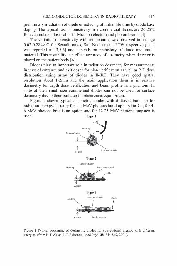
Diodes play an important role in radiation dosimetry for measurements in vivo of entrance and exit doses for plan verification as well as 2 D dose distribution using array of diodes in IMRT. They have good spatial resolution about 1-2mm and the main application them is in relative dosimetry for depth dose verification and beam profile in a phantom. In spite of their small size commercial diodes can not be used for surface dosimetry due to their build up for electronics equilibrium.
Figure 1 shows typical dosimetric diodes with different build up for radiation therapy. Usually for 1-4 MeV photons build up is Al or Cu, for 4-6 MeV photons bras is an option and for 12-25 MeV photons tungsten is used.
Figure 1 Typical packaging of dosimetric diodes for conventional therapy with different energies. (from K.T.Welsh, L.E.Reinstein, Med.Phys. 28, 844-849, 2001).
A.B. ROSENFELD 116
Diodes have found application in proton therapy relative dosimetry due to it low size, however still exist some disagreement between amplitude of Bragg peak relative to entrance dose derived with ionizing chambers and measured with diode in a water tank. This 2-3% disagreement possibly due to increasing of LET of protons and related to them changing of injection level in a diode leading to different recombination properties in comparison to entrance conditions.
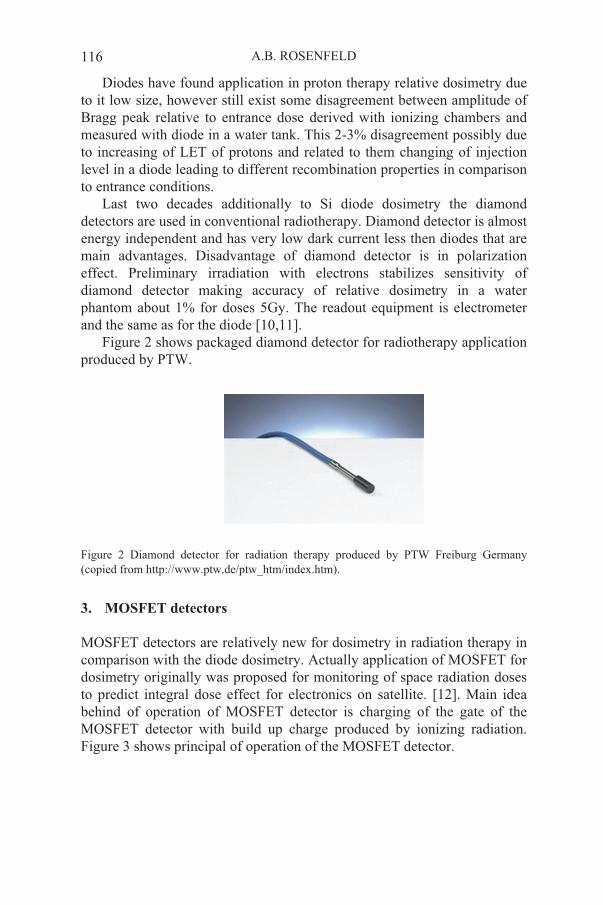
Last two decades additionally to Si diode dosimetry the diamond detectors are used in conventional radiotherapy. Diamond detector is almost energy independent and has very low dark current less then diodes that are main advantages. Disadvantage of diamond detector is in polarization effect. Preliminary irradiation with electrons stabilizes sensitivity of diamond detector making accuracy of relative dosimetry in a water phantom about 1% for doses 5Gy. The readout equipment is electrometer and the same as for the diode [10,11].
Figure 2 shows packaged diamond detector for radiotherapy application produced by PTW.
Figure 2 Diamond detector for radiation therapy produced by PTW Freiburg Germany (copied from http://www.ptw.de/ptw_htm/index.htm).
3. MOSFET detectors
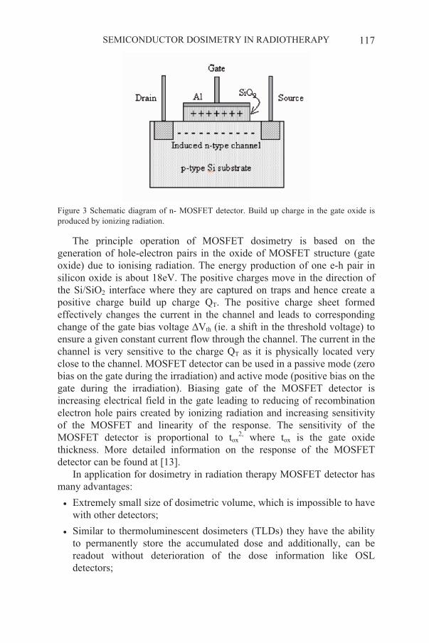
MOSFET detectors are relatively new for dosimetry in radiation therapy in comparison with the diode dosimetry. Actually application of MOSFET for dosimetry originally was proposed for monitoring of space radiation doses to predict integral dose effect for electronics on satellite. [12]. Main idea behind of operation of MOSFET detector is charging of the gate of the MOSFET detector with build up charge produced by ionizing radiation. Figure 3 shows principal of operation of the MOSFET detector.
SEMICONDUCTOR DOSIMETRY IN RADIOTHERAPY 117
Figure 3 Schematic diagram of n- MOSFET detector. Build up charge in the gate oxide is produced by ionizing radiation.
The principle operation of MOSFET dosimetry is based on the generation of hole-electron pairs in the oxide of MOSFET structure (gate oxide) due to ionising radiation. The energy production of one e-h pair in silicon oxide is about 18eV. The positive charges move in the direction of the Si/SiO2 interface where they are captured on traps and hence create a positive charge build up charge QT. The positive charge sheet formed effectively changes the current in the channel and leads to corresponding change of the gate bias voltage Vth (ie. a shift in the threshold voltage) to ensure a given constant current flow through the channel. The current in the channel is very sensitive to the charge QT as it is physically located very close to the channel. MOSFET detector can be used in a passive mode (zero bias on the gate during the irradiation) and active mode (positive bias on the gate during the irradiation). Biasing gate of the MOSFET detector is increasing electrical field in the gate leading to reducing of recombination electron hole pairs created by ionizing radiation and increasing sensitivity of the MOSFET and linearity of the response. The sensitivity of the MOSFET detector is proportional to tox
2, where tox is the gate oxide thickness. More detailed information on the response of the MOSFET detector can be found at [13].
In application for dosimetry in radiation therapy MOSFET detector has many advantages:
Extremely small size of dosimetric volume, which is impossible to have with other detectors;
Similar to thermoluminescent dosimeters (TLDs) they have the ability to permanently store the accumulated dose and additionally, can be readout without deterioration of the dose information like OSL detectors;
A.B. ROSENFELD 118
They are dose rate independent up to 108Gy/s.
Their sensitivity can be adjusted by gate bias, which makes them suitable in many applications in radiotherapy.
It can be readout after irradiation or in real time making possibility for real time QA or dose profiling in a water phantom.
They are currently relatively cheap and can be disposable utilizing “one dose” principle.
All above mentioned advantages of the MOSFET detector make them useful for dosimetry in the field of strong electronic disequilibrium like on the surface of the body or anatomical cavities and in build up regions of depth dose curves in case of irradiation on MV range X-rays on medical LINACs. Centre for Medical Radiation Physics, University of Wollongong (CMRP) is developer of clinical MOSFET dosimetry systems and has got extensive experience with their applications on different radiation oncology modalities. In this paper we will present overview of these applications and findings.
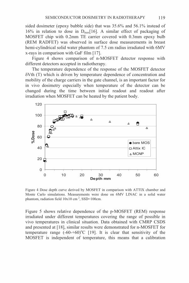
MOSFET clinical dosimetry system was investigated was investigated in electron and photon radiation field of VARIAN 2100C at 100cm SSD with various beam configurations: field size from 2x2 cm to 40x40 cm, with 10mm Perspex block tray and 15 wedge. The MOSFET detector was situated in the central axis of the beam on a surface of solid water phantom followed by measurements in the same field by TLD and ATTIX chamber. For all fields the agreement between ATTIX, TLD and MOSFET in percentage of surface dose relative to Dmax was better than 1% [14]. These results were obtained for 6MeV and 18MeV phantom fields and 6, 9, 12, 16, 20 MeV electron fields. The most impressive application of MOSFET detector is in a surface dosimetry.
Neither TLD nor diodes can be used for direct reading of the surface dose due to their size of dosimetric volume. In high-energy electron fields the TLD detector systematically showed 2% surface dose more than the ATTIX chamber while our MOSFETs were in an excellent agreement with ATIX chamber and Monet Carlo simulations. Ability to measure the surface dose utilizing advantages of the MOSFET detector depends on packaging of this detectors. It is exist trade off between protection of the MOSFET from environment factors and effective depth of measurement [15]. Most producers of MOSFET detectors have a KAPTON or thin PC board carrier with epoxy bubble on the top of MOSFET detector. For the TN MOSFET the chip is mounted on a KAPTON carrier and covered by 1mm epoxy coating. The equivalent depth in water for TN MOSFET sensors was 0.8 mm for the flat-sided dosimeter and 1.8 mm for the round
SEMICONDUCTOR DOSIMETRY IN RADIOTHERAPY 119
sided dosimeter (epoxy bubble side) that was 35.6% and 56.1% instead of 16% in relation to dose in Dmax[16]. A similar effect of packaging of MOSFET chip with 0.2mm TE carrier covered with 0.3mm epoxy bulb (REM RADFET) was observed in surface dose measurements in breast hemi-cylindrical solid water phantom of 7.5 cm radius irradiated with 6MV x-rays in comparison with GaF film [17].
Figure 4 shows comparison of n-MOSFET detector response with different detectors accepted in radiotherapy.
The temperature dependence of the response of the MOSFET detector Vth (T) which is driven by temperature dependence of concentration and
mobility of the charge carriers in the gate channel, is an important factor for in vivo dosimetry especially when temperature of the detector can be changed during the time between initial readout and readout after irradiation when MOSFET can be heated by the patient body.
0
20
40
60
80
100
120
0 10 20 30 40 50 60Depth mm
% D
os
e
bare MOS
Attix IC
MCNP
Figure 4 Dose depth curve derived by MOSFET in comparison with ATTIX chamber and Monte Carlo simulations. Measurements were done on 6MV LINAC in a solid water phantom, radiation field 10x10 cm 2, SSD=100cm.
Figure 5 shows relative dependence of the p-MOSFET (REM) response irradiated under different temperatures covering the range of possible in vivo temperatures in clinical situation. Data obtained with CMRP CSDS and presented at [18], similar results were demonstrated for n-MOSFET for temperature range (-60-+60)oC [19]. It is clear that sensitivity of the MOSFET is independent of temperature, this means that a calibration
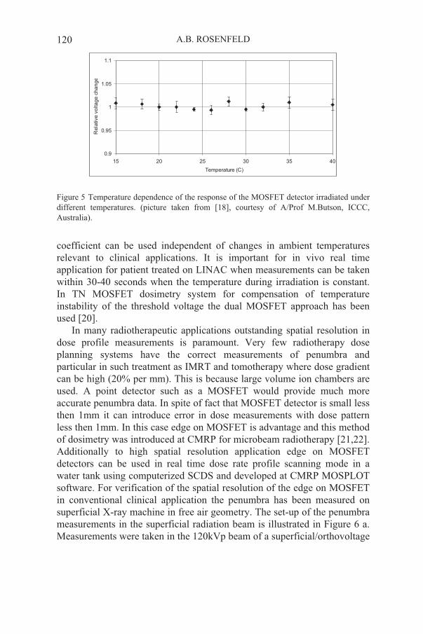
A.B. ROSENFELD 120
0.9
0.95
1
1.05
1.1
15 20 25 30 35 40
Temperature (C)
Re
lative
vo
lta
ge
ch
an
ge
Figure 5 Temperature dependence of the response of the MOSFET detector irradiated under different temperatures. (picture taken from [18], courtesy of A/Prof M.Butson, ICCC, Australia).
coefficient can be used independent of changes in ambient temperatures relevant to clinical applications. It is important for in vivo real time application for patient treated on LINAC when measurements can be taken within 30-40 seconds when the temperature during irradiation is constant. In TN MOSFET dosimetry system for compensation of temperature instability of the threshold voltage the dual MOSFET approach has been used [20].
In many radiotherapeutic applications outstanding spatial resolution in dose profile measurements is paramount. Very few radiotherapy dose planning systems have the correct measurements of penumbra and particular in such treatment as IMRT and tomotherapy where dose gradient can be high (20% per mm). This is because large volume ion chambers are used. A point detector such as a MOSFET would provide much more accurate penumbra data. In spite of fact that MOSFET detector is small less then 1mm it can introduce error in dose measurements with dose pattern less then 1mm. In this case edge on MOSFET is advantage and this method of dosimetry was introduced at CMRP for microbeam radiotherapy [21,22]. Additionally to high spatial resolution application edge on MOSFET detectors can be used in real time dose rate profile scanning mode in a water tank using computerized SCDS and developed at CMRP MOSPLOT software. For verification of the spatial resolution of the edge on MOSFET in conventional clinical application the penumbra has been measured on superficial X-ray machine in free air geometry. The set-up of the penumbra measurements in the superficial radiation beam is illustrated in Figure 6 a. Measurements were taken in the 120kVp beam of a superficial/orthovoltage
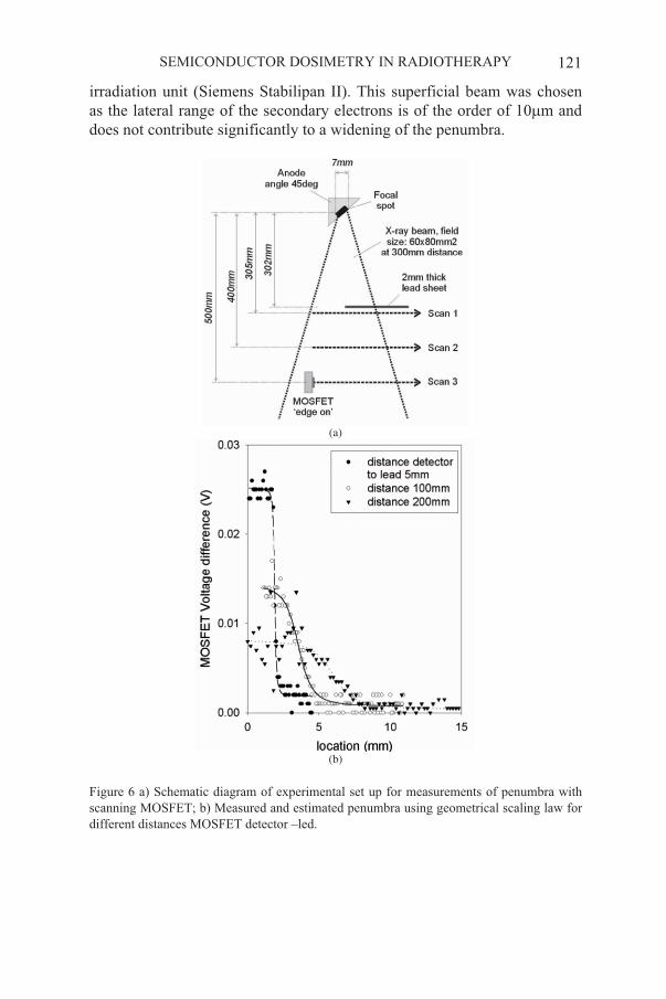
SEMICONDUCTOR DOSIMETRY IN RADIOTHERAPY 121
irradiation unit (Siemens Stabilipan II). This superficial beam was chosen as the lateral range of the secondary electrons is of the order of 10 m and does not contribute significantly to a widening of the penumbra.
(a)
(b)
Figure 6 a) Schematic diagram of experimental set up for measurements of penumbra with scanning MOSFET; b) Measured and estimated penumbra using geometrical scaling law for different distances MOSFET detector –led.
A.B. ROSENFELD 122
The beam was collimated using a metal cone with a field size definition of 8 x 10 cm2 at 30cm distance from the focal spot. A 3mm thick lead sheet was placed at 30.2 cm distance from the focal spot to create a sharp beam edge at the field centre. Lead of 3mm thickness attenuates the beam to less than 1% of the incoming intensity. The penumbra was scanned in both directions (from beam to out of beam and reverse) at three different distances from the lead sheet (0.5cm, 10cm and 20cm) in anode-cathode direction. The scanning step was 0.1mm/s that was determined by water tank scanning system. Figure 6b shows results of measured penumbra and estimated using geometrical scaling law. From the difference between the theoretical and the measured penumbra at close distance to the lead shield one can estimate the spatial resolution of the edge on MOSFET detector to be better than 0.1mm. More details on this experiment can be written in our paper [23].
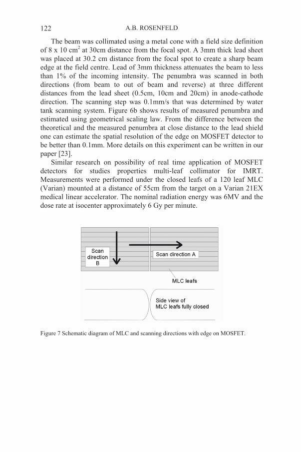
Similar research on possibility of real time application of MOSFET detectors for studies properties multi-leaf collimator for IMRT. Measurements were performed under the closed leafs of a 120 leaf MLC (Varian) mounted at a distance of 55cm from the target on a Varian 21EX medical linear accelerator. The nominal radiation energy was 6MV and the dose rate at isocenter approximately 6 Gy per minute.
Figure 7 Schematic diagram of MLC and scanning directions with edge on MOSFET.
SEMICONDUCTOR DOSIMETRY IN RADIOTHERAPY 123
(a)
(b)
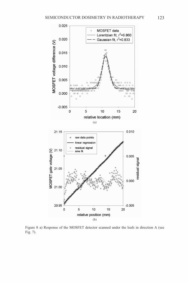
Figure 8 a) Response of the MOSFET detector scanned under the leafs in direction A (see Fig. 7).

A.B. ROSENFELD 124
Figure 8a shows the results of the detector scan in parallel to the MLC leaf moving direction (scan A in Figure 7), i.e. inter leaf leakage. The full width half maximum (FWHM) of the Lorentzian fit was 2.5mm. The maximum dose rate between the two leafs is of the order of 15% of the dose in the respective open radiation field that match well to data obtained by others [24].
Figure 8b shows the results of the dosimetric scan of interleaf leakage (scan B in Figure 7). The raw data points show the change of gate voltage with accumulated dose. As the detector scan speed is constant, the relative position is also proportional to the overall dose received due to the radiation background under the closed MLC, i.e. leakage and transmission. It shows that MOSFET detector is sensitive enough to measure the interleaf leakage. The data was fitted using a sinusoidal function. The best fit had a period of 4.82mm which is well compatible with the leaf width of 5mm. Compared to the dose rate in the open field, this indicates that the interleaf leakage is at least 3% of the open field dose, a measurement that would be extremely difficult to obtain with any other technique. More detailed analysis of the spatial resolution real time scanning MOSFET SCDS is presented in our papers [23,27].
Micron spatial resolution of the MOSFET detectors was also proved for synchrotron microbeam radiation therapy (MRT), which is a very promising new radiation modality. This modality is utilizes high dose rate array of synchrotron microbeams with microbeam width about 25-30 microns and pitch 200-400 microns [25,26]. Dosimetry of within single microbeam with micron and submicron resolution and in accurately measuring the microbeam dose in the peaks and valleys is an important parameter to determine the quality of microbeam treatment.
While Monte Carlo simulations are valuable tool for prediction of dose in MRT experimental verification of simulations is important [27-30]. Edge on MOSFET dosimetry in MRT is another example of high spatial resolution of semiconductor detectors in modern radiation therapy. Comparison of experimental results obtained with MOSFET dosimetry with GAF film and simulations is a subject of continuous collaboration between CMRP and ESRF. Figure 9 shows example of dosimetry of three subsequent microbeams of MRT array obtained at ESRF with edge on MOSFET detectors and automatic scanning system. Figure 10 shows the response of gafchromic film (GaF) for the same array of microbeams measured in the Perspex phantom Fig. 11 shows one of the CMRP SCDS.

SEMICONDUCTOR DOSIMETRY IN RADIOTHERAPY 125
Figure 9 Relative response of edge on MOSFET CSCD measured in scanning mode with 5 m steps at ESRF MRT facility, beam line ID17 for three consecutive microbeams 25 m
width and 400 m pitch scanned. This result is a collaborative research between CMRP and ESRF.
Figure 10 Dosimetry of array of synchrotron microbeams at ESRF MRT facility with GaF film. Two regions are presented are corresponding to array of microbeams with pitch 400 mand 200 m the beam width is 25 m. Readout of the film was done by high spatial resolution optical imager. Courtesy of Dr Elke Brauer-Krich, ESRF. [32].

A.B. ROSENFELD 126
Figure 11 Real time scanning MOSFET clinical dosimetry system (SCDS) developed and produced by CMRP.
Previous discussion of semiconductor detectors were limited to high dose applications relevant to in direct radiation therapy beam however CSDS MOSFET also found useful in peripheral dosimetry on medical LINACs outside of the radiation field where doses are in the dose range 2-10 cGy demonstrating accuracy slightly better then TLD detectors [33].
A lot of work in the last ten years has been done on MOSFET detectors in conventional radiation therapy by other colleagues and useful information can be found in papers referred in [30,33,34] as well as mostly in Medical Physics Journal, Phys. Med. Biology, Int. J. Radiation Oncology, Physics and Biol. and using Medline search system for MOSFET dosimetry. The scope of this paper does not allow review all publications in this field and all aspects related to MOSFET dosimetry.
Additionally to electron and photon therapies MOSFET detectors reveal themselves useful in neutron therapies. In Boron Neutron Capture Therapy (BNCT) application of dual MOSFET detectors with one of them covered with B-10 converter useful for measurements of thermal neutron flux distribution in a phantom [35]. This was possible due to very high sensitivity of the MOSFET to alpha particles irradiation. Figure 12 shows the response of the MOSFET detector to alpha particles from low intensity alpha source. However the effect of high LET particles on build up charge in the gate oxide still under consideration.

SEMICONDUCTOR DOSIMETRY IN RADIOTHERAPY 127
Figure 12 The integral response of an n-MOSFET with a thick oxide layer about 1 micron to 5.48 MeV alpha particles from 241Am with a fluence of about 4x103 cm-2s-1.
Concept of application of MOSFET detectors for simultaneous integral dosimetry and microdosimetry at the same point of phantom in FNT was introduced in [36] and became original concept for development of proportional silicon microdosimetry. Recently was demonstrated that application of MOSFET detectors can be useful for gamma integral dosimetry in mixed gamma neutron field which exist in Fast Neutron Therapy in conjunction with PIN diodes that will be discussed later.
4. Semiconductor radiation detectors in hadron therapy
4.1. INTEGRAL DOSIMETRY IN NEUTRON THERAPY WITH PIN DIODES
Radiation semiconductor detectors considered in the previous section were operating on the ionization energy loses (IEL) principle.
Bulk radiation damage in semiconductor devices is proportional to Non Ionizing Energy Losses (NEIL) leading to displacement of atoms from their sites. Change in the electrical characteristics of devices affected by atomic displacement is a suitable monitor of NIEL. One can measure the effects of NIEL by monitoring the change in lifetime, diffusion length, or concentration (compensation) of charge carriers. This approach formed a special class of silicon radiation detectors suitable for neutron and proton radiotherapy. The forward bias voltage drop change in special silicon diode is a good monitor of NIEL. General theory of the response of p-i-n diodes with a long base to fast neutron radiation was considered in details in [37,38]. It was demonstrated that permanent degradation of lifetime and concentration of the charge carriers due radiation defect is a reason for
A.B. ROSENFELD 128
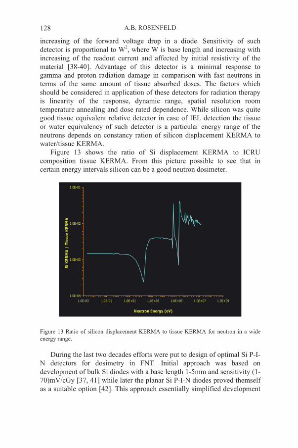
increasing of the forward voltage drop in a diode. Sensitivity of such detector is proportional to W2, where W is base length and increasing with increasing of the readout current and affected by initial resistivity of the material [38-40]. Advantage of this detector is a minimal response to gamma and proton radiation damage in comparison with fast neutrons in terms of the same amount of tissue absorbed doses. The factors which should be considered in application of these detectors for radiation therapy is linearity of the response, dynamic range, spatial resolution room temperature annealing and dose rated dependence. While silicon was quite good tissue equivalent relative detector in case of IEL detection the tissue or water equivalency of such detector is a particular energy range of the neutrons depends on constancy ration of silicon displacement KERMA to water/tissue KERMA.
Figure 13 shows the ratio of Si displacement KERMA to ICRU composition tissue KERMA. From this picture possible to see that in certain energy intervals silicon can be a good neutron dosimeter.
1.0E-04
1.0E-03
1.0E-02
1.0E-01
1.0E-03 1.0E-01 1.0E+01 1.0E+03 1.0E+05 1.0E+07 1.0E+09
Neutron Energy (eV)
Si
KE
RM
A /
Tis
su
e K
ER
MA
Figure 13 Ratio of silicon displacement KERMA to tissue KERMA for neutron in a wide energy range.
During the last two decades efforts were put to design of optimal Si P-I-N detectors for dosimetry in FNT. Initial approach was based on development of bulk Si diodes with a base length 1-5mm and sensitivity (1-70)mV/cGy [37, 41] while later the planar Si P-I-N diodes proved themself as a suitable option [42]. This approach essentially simplified development
SEMICONDUCTOR DOSIMETRY IN RADIOTHERAPY 129
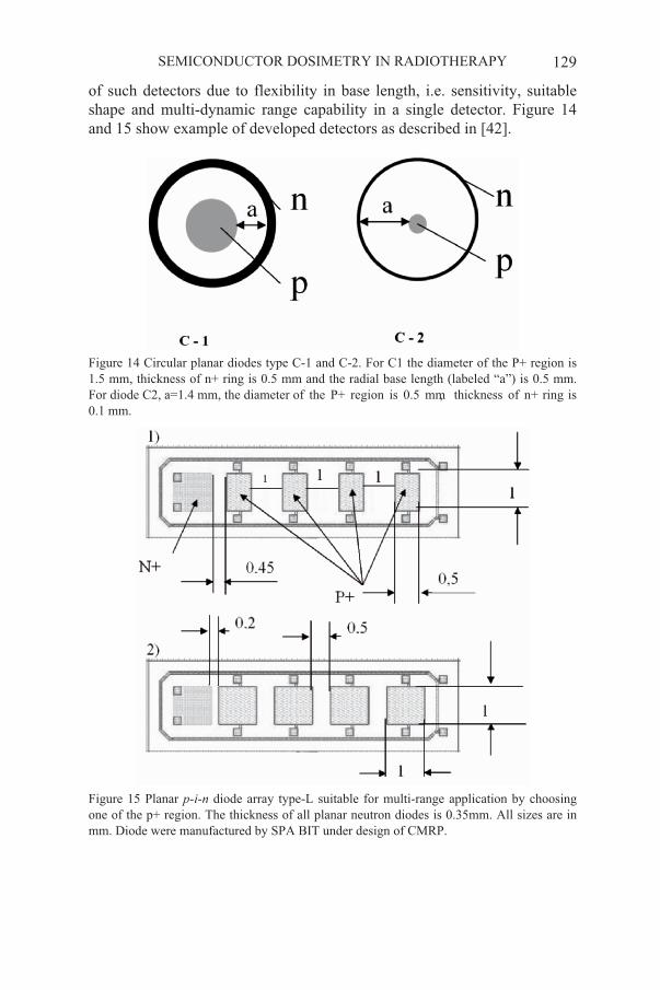
of such detectors due to flexibility in base length, i.e. sensitivity, suitable shape and multi-dynamic range capability in a single detector. Figure 14 and 15 show example of developed detectors as described in [42].
Figure 14 Circular planar diodes type C-1 and C-2. For C1 the diameter of the P+ region is 1.5 mm, thickness of n+ ring is 0.5 mm and the radial base length (labeled “a”) is 0.5 mm.
Figure 15 Planar p-i-n diode array type-L suitable for multi-range application by choosing one of the p+ region. The thickness of all planar neutron diodes is 0.35mm. All sizes are in mm. Diode were manufactured by SPA BIT under design of CMRP.
0.1 mm.For diode C2, a=1.4 mm, the diameter of the P+ region is 0.5 mm, thickness of n+ ring is
A.B. ROSENFELD 130
Characterization of gamma and neutron components in FNT beam in a water phantom is an important part of QA because their radiobiological properties are different. Traditionally a paired detector method is applied for separate dosimetry of in mixed gamma neutron radiation fields which is based on TE ionizing chamber and miniature Geiger-Müller (G-M) counter. First detector has sensitivity almost equal to gamma and neutrons while second one most sensitive to gamma radiation. However, the results obtained with TE/ G-M pair detectors have an inaccuracy of up to 8% resulting from the error in estimating the neutron sensitivity ( UK ) value of the G-M counter.[44].
The application of the diodes to characterize d(48.5)+Be fast neutron beams produced at superconducting cyclotron in Harper Hospital [43] have shown results that are very comparable with those obtained with the traditional pair detector method, which is time consuming. In the measurements of the lateral beam profile, the diodes have shown a very good agreement with the profiles obtained with pair detector method. The superior spatial resolution of the diode produced a sharper penumbra compared with the bigger size ionization chamber. For central axis depth dose measurements, both diodes showed an excellent agreement with the results obtained with pair detector method. All diodes were calibrated at depth 5 cm in a water tank with well known fast neutron dose, all diodes were encapsulated in TE A150 plastic with thickness enough for charge particle equilibrium.
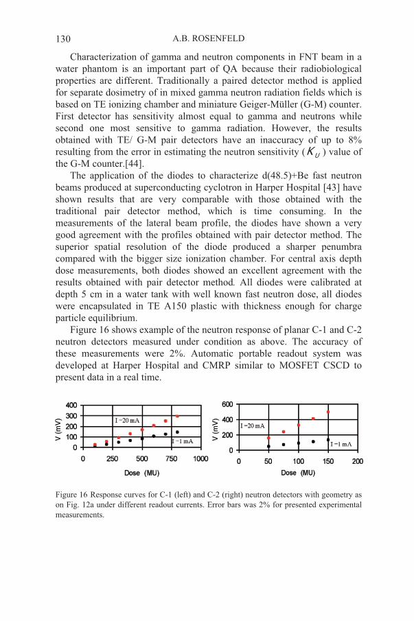
Figure 16 shows example of the neutron response of planar C-1 and C-2 neutron detectors measured under condition as above. The accuracy of these measurements were 2%. Automatic portable readout system was developed at Harper Hospital and CMRP similar to MOSFET CSCD to present data in a real time.
Figure 16 Response curves for C-1 (left) and C-2 (right) neutron detectors with geometry as on Fig. 12a under different readout currents. Error bars was 2% for presented experimental measurements.
SEMICONDUCTOR DOSIMETRY IN RADIOTHERAPY 131
Bulk and planar neutron integral detectors can be used to derive neutron doses in radiation fields with different contribution of gamma dose.Different depths and attenuation conditions produced beams with gamma contribution to the total dose ranging from 4 to 16.6%. The diode demonstrated a good accuracy in terms of measuring neutron and total dose. In measuring gamma component, the diode was accurate to within ± 2.5 cGy. Measurements of neutron dose with bulk neutron diode in different radiation fields are presented in Tabl.1.
Agreement in dosimetry with paired detector method is within 7% that is within uncertainty of paired method as mentioned above. Good agreement has been achieved between for planar diodes as well.
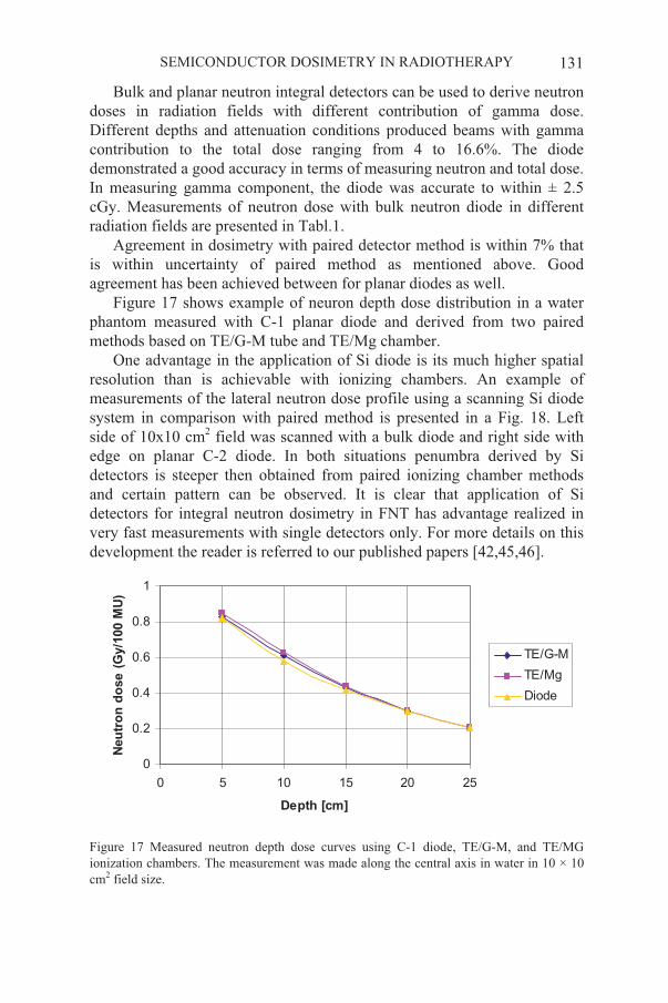
Figure 17 shows example of neuron depth dose distribution in a water phantom measured with C-1 planar diode and derived from two paired methods based on TE/G-M tube and TE/Mg chamber.
One advantage in the application of Si diode is its much higher spatial resolution than is achievable with ionizing chambers. An example of measurements of the lateral neutron dose profile using a scanning Si diode system in comparison with paired method is presented in a Fig. 18. Left side of 10x10 cm2 field was scanned with a bulk diode and right side with edge on planar C-2 diode. In both situations penumbra derived by Si detectors is steeper then obtained from paired ionizing chamber methods and certain pattern can be observed. It is clear that application of Si detectors for integral neutron dosimetry in FNT has advantage realized in very fast measurements with single detectors only. For more details on this development the reader is referred to our published papers [42,45,46].
0
0.2
0.4
0.6
0.8
1
0 5 10 15 20 25
Depth [cm]
Neu
tro
n d
ose (G
y/1
00 M
U)
TE/G-M
TE/Mg
Diode
Figure 17 Measured neutron depth dose curves using C-1 diode, TE/G-M, and TE/MG ionization chambers. The measurement was made along the central axis in water in 10 × 10 cm2 field size.
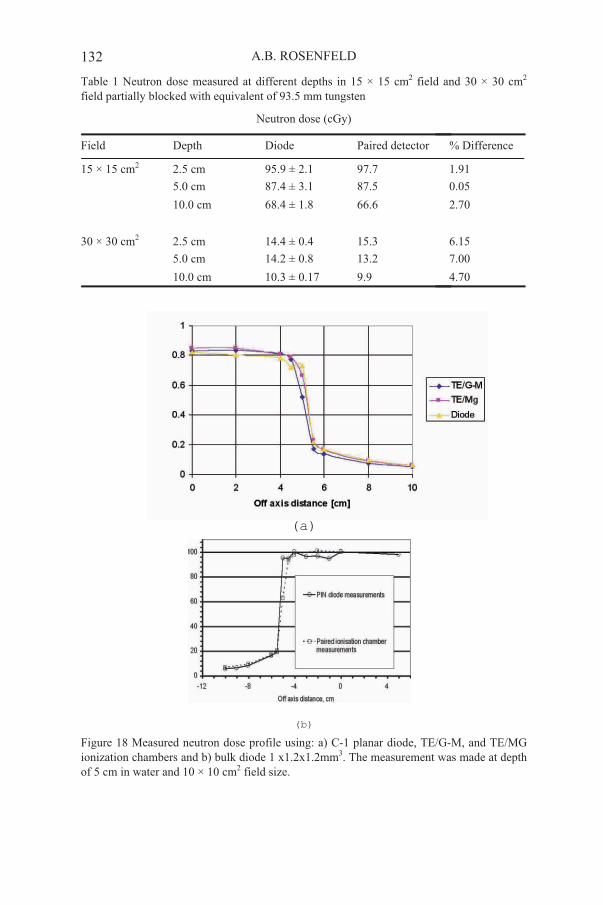
A.B. ROSENFELD 132
Table 1 Neutron dose measured at different depths in 15 × 15 cm2 field and 30 × 30 cm2
field partially blocked with equivalent of 93.5 mm tungsten
Neutron dose (cGy)
Field Depth Diode Paired detector % Difference
15 × 15 cm2 2.5 cm 95.9 ± 2.1 97.7 1.91
5.0 cm 87.4 ± 3.1 87.5 0.05
10.0 cm 68.4 ± 1.8 66.6 2.70
30 × 30 cm2 2.5 cm 14.4 ± 0.4 15.3 6.15
5.0 cm 14.2 ± 0.8 13.2 7.00
10.0 cm 10.3 ± 0.17 9.9 4.70
(a)
(b)
Figure 18 Measured neutron dose profile using: a) C-1 planar diode, TE/G-M, and TE/MG ionization chambers and b) bulk diode 1 x1.2x1.2mm3. The measurement was made at depth of 5 cm in water and 10 × 10 cm2 field size.
SEMICONDUCTOR DOSIMETRY IN RADIOTHERAPY 133
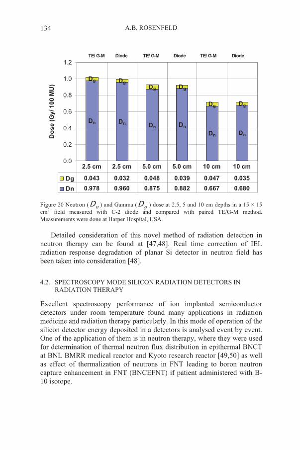
Single planar Si p-i-n diodes can be used as dual detector in mixed gamma neutron field measuring independently gamma and neutron dose rates at the same point. It can be achieved by combination of IEL and NIEL readout from the same detector. NIEL are related to neutron dosimetry as was demonstrated in this paper. IEL component measured by induced radiation current with the same diode in a water phantom is not representing gamma dose only. Neutron component of the field is making contribution to IEL through recoil protons. While calibration of IEL response of C type planar passive “vertical” diode (p-n junction between P+ core and rear n+side) connected to electrometer was carried out on Co-60 source at Harper Hospital with accuracy better then 2%, it can be attributed to protons due to slightly different ratio of stoping power electrons and protons in water to silicon. Another factor is related to different mode recombination of charge produced by protons and Compton electrons having in mind that plasma track density form proton much higher then from electron. This is why separate calibration of Si planar diode in IEL mode to neutron is required. Using two modes of readout: forward voltage change and current (IEL) mode the paired detector method can be arranged with a single planar Si detector. Figure 19 shows schematic approach of this method utilizing planar Si detector with multi dynamic range capabilities.
Figure 19 Dual Si planar detector for simultaneous measurement of neutron and gamma components of neutron field. Subsequent readout of collected charge and change of the forward voltage from single detector substitute in real time the paired detector method. (Developed at CMRP and realized in collaboration with Harper Hospital, USA.
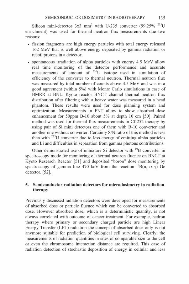
Figure 20 shows one of the initial results of gamma and neutron doses measurements with a single detector in FNT and comparison them with paired method.
A.B. ROSENFELD 134
TE/ G-M Diode TE/ G-M Diode TE/ G-M Diode
Dn Dn
Dn Dn
DnDn
Dg Dg
Dg Dg
DgDg
0.0
0.2
0.4
0.6
0.8
1.0
1.2
Do
se
(G
y/ 1
00
MU
)
Dg 0.043 0.032 0.048 0.039 0.047 0.035
Dn 0.978 0.960 0.875 0.882 0.667 0.680
2.5 cm 2.5 cm 5.0 cm 5.0 cm 10 cm 10 cm
Figure 20 Neutron ( nD ) and Gamma ( gD ) dose at 2.5, 5 and 10 cm depths in a 15 × 15 cm2 field measured with C-2 diode and compared with paired TE/G-M method. Measurements were done at Harper Hospital, USA.
Detailed consideration of this novel method of radiation detection in neutron therapy can be found at [47,48]. Real time correction of IEL radiation response degradation of planar Si detector in neutron field has been taken into consideration [48].
4.2. SPECTROSCOPY MODE SILICON RADIATION DETECTORS IN RADIATION THERAPY
Excellent spectroscopy performance of ion implanted semiconductor detectors under room temperature found many applications in radiation medicine and radiation therapy particularly. In this mode of operation of the silicon detector energy deposited in a detectors is analysed event by event. One of the application of them is in neutron therapy, where they were used for determination of thermal neutron flux distribution in epithermal BNCT at BNL BMRR medical reactor and Kyoto research reactor [49,50] as well as effect of thermalization of neutrons in FNT leading to boron neutron capture enhancement in FNT (BNCEFNT) if patient administered with B-10 isotope.
SEMICONDUCTOR DOSIMETRY IN RADIOTHERAPY 135
Silicon mini-detector 3x3 mm2 with U-235 converter (99.25% 235Uenrichment) was used for thermal neutron flux measurements due two reasons:
fission fragments are high energy particles with total energy released 162 MeV that is well above energy deposited by gamma radiation or recoil protons in a detector;
spontaneous irradiation of alpha particles with energy 4.5 MeV allow real time monitoring of the detector performance and accurate measurements of amount of 235U isotope used in simulation of efficiency of the converter to thermal neutron. Thermal neutron flux was measured by total number of counts above 4.5 MeV and was in a good agreement (within 5%) with Monte Carlo simulations in case of BMRR at BNL. Kyoto reactor BNCT channel thermal neutron flux distribution after filtering with a heavy water was measured in a head phantom. These results were used for dose planning system and optimization. Measurements in FNT allow to show absorbed dose enhancement for 50ppm B-10 about 5% at depth 10 cm [50]. Paired method was used for thermal flux measurements in Cf-252 therapy by using pair of Si mini detectors one of them with B-10 converter and another one without converter. Certainly S/N ratio of this method is less then with 235U converter due to less energy of emitting alpha particles and Li and difficulties in separation from gamma photons contributions.
Other demonstrated use of miniature Si detector with 10B converter in spectroscopy mode for monitoring of thermal neutron fluence on BNCT at Kyoto Research Reactor [51] and deposited “boron” dose monitoring by spectroscopy of gamma line 470 keV from the reaction 10B(n, ) Ge detector. [52].
5. Semiconductor radiation detectors for microdosimetry in radiation therapy
Previously discussed radiation detectors were developed for measurements of absorbed dose or particle fluence which can be converted to absorbed dose. However absorbed dose, which is a deterministic quantity, is not always correlated with outcome of cancer treatment. For example, hadron therapy where primary or secondary charged particle are high Linear Energy Transfer (LET) radiation the concept of absorbed dose only is not anymore suitable for prediction of biological cell surviving. Clearly, the measurements of radiation quantities in sites of comparable size to the cell or even the chromosome interaction distance are required. This case of radiation detection of stochastic deposition of energy in cellular and less
A.B. ROSENFELD 136
sizes characteristic volumes well known as microdosimetry. Of utility in such measurements was the development in the early 1950s of the low-pressure proportional counter (TEPC), commonly called the Rossi counter after its pioneer [53]. More detailed information on microdosimetry concepts can be found in [54,55].
In microdosimetry we are doing spectroscopy of events of deposited energy from single particle in a small sensitive water/tissue equivalent volumes. By introduction of lineal energy as a y=E/<l>, where E is a deposited energy and <l> is an average chord of the sensitive volume, possible conversion of MCA spectra to microdosimetric spectra f(y) vs y.
Microdosimetric measurements are a valuable supplement to radiobiological studies in the characterization of Relative Biological Effectiveness (RBE) of therapeutic beams. The traditional experimental tool for microdosimetric measurements is the tissue equivalent proportional counter (TEPC). The TEPC does however have several shortcomings outlined in [55]. Recent developments have been made which propose the use of silicon based microdosimeters as a viable alternative to the TEPC [55-59].
A silicon based microdosimeter must satisfy the following criterion: it must possess a well defined charge collection volume, be of a small size to simulate the biological cell, be able to measure LET down to 1 keV/ m or less, be able to provide tissue equivalent (TE) measurements and an array of microdosimeters is needed to maximise counting statistics.
A prototype silicon microdosimeter has been produced at the Centre for Medical Radiation Physics (CMRP) which presents a viable alternative to the TEPC. The device consists of an array of microscopic planar p-n junction diodes manufactured by Fujitsu Research Laboratories. The diodes are connected in parallel and are reverse biased. Charge collected by the device from a passing ion is indicative of ion LET. SOI (silicon-on-insulator) technology precludes charge collection from beneath the junction, facilitating a well defined charge collection region. The wafer thickness’ currently available are 2, 5, and 10 m. Several diode sizes are available and to date those tested on high LET radiation therapy beams have an area of 10 x 10 m2, with 120 x 40 = 4800 diodes in the array. To a first approximation, the sensitive volume has a Right Angled Parallelepiped (RPP) shape, hence the chord length distribution will differ from the spherical TEPC. The issue of tissue equivalence has also been addressed in the literature [56]. Readout of such silicon detector required usual nuclear spectroscopy set up. Portable version of CMRP silicon microdosimeter show on Fig. 21.
SEMICONDUCTOR DOSIMETRY IN RADIOTHERAPY 137
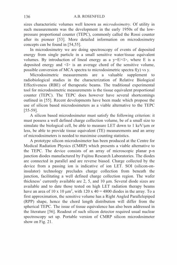
Figure 21 Low noise microdosimetric probe with Lucite TE material and aluminum shield absent. Left chip is SOI microdosimetric chip as described in our papers. Small size low noise hybrid charge sensitive preamplifier A250 and shaping amplifier were mounted on a board close to microdosimeter and demonstrated good performance.
Testings of silicon microdosimeters were performed on different radiation oncology modalities including in reactor based BNCT (Kyoto University Research Reactor (KUR), Japan and BMRR BNL, USA) and accelerator based Boron Neutron Capture Synovectomy (BNCS) (Laboratory for Accelerator Beam Applications (LABA), MIT, USA), Proton therapy (Northeastern Proton Therapy Center, NPTC, Boston, and Loam Linda University Medical Centre, LLUMC, USA), and Fast Neutron Therapy (Harper Hospital, Detroit, USA).
For BNCT microdosimetry, microdosimetry measurements are performed with a boron coating on the microdosimeter, or with boron introduced directly into the microdosimeter. Advantage of the silicon SOI microdosimeter for BNCT that 10B uptake by cell can be modelled in a silicon cell (p-n junction of array) by P+ implanted region, by choosing of p-type base of SOI device or with a 10B converter above chip. It can model different spatial distribution of 10B uptake in a cell that is impossible to do with TEPC. For the presented microdosimetric spectra here, the boron concentration already present in the p+ region of the device was used as a crude analogy to boron uptake in the cell nucleus, as in [60]. Silicon 2D microdosimetry as described allow to model such radiobiological effects as a cross fire between cells in BNCT by producing adjacent silicon cells with and without 10B, for example.
Below presented as an example lineal energy (microdosimetric) spectra obtained with SOI microdosimeter at KUR BNCT facility and BNCS facility at MIT. Both reactor BNCT beam (KUR), and accelerator based BNCS beam measurements were performed using the 2 m SOI device, at similar depths in a water phantom.
A.B. ROSENFELD 138
The KUR reactor is a 5 MW reactor, running continuously at full power [14]. For BNCT, the reactor may be operated in three modes depending on combinations of heavy water, boral, and cadmium filters [14]. Each mode has a characteristic neutron energy spectrum and thermal neutron flux depth distribution. The first mode is "thermal", with no boral and cadmium filters and some attenuation with heavy water. This mode is used for superficial tumours. The second is "mixed mode", a thermal neutron mode without filters for higher thermal neutron flux and is aimed at tumours 1-2cm depth. This mode is used for present clinical trials and for the present experiments. The final mode is "epithermal", predominantly aimed for deep seated tumours.
A cylindrical water head phantom was used, with its axis aligned with that of the beam. The low noise microdosimeter probe was positioned on the central axis of beam and measurements were performed at 1cm depth using the 2 m and 5 m SOI devices reversed biased to 10 V.
Measurements were also performed at the accelerator based BNCS facility at MIT. Neutrons were produced by bombarding a beryllium target with 1.5 MeV deuterons via the 9Be(d,n)10B reaction. The beam is then moderated from its initial 1 MeV using heavy water. Accelerator based BNCT possesses a high recoil proton component relative to reactor based BNCT.
The target was located within a 9 cm diameter 23 cm length cylindrical heavy water moderator encapsulated in an 18cm thick graphite reflector which improves the target dose rate [11]. The detector was placed at a depth of 1.5 cm, on axis, in a 28.5x28.5x21.5 cm3 water phantom. Microdosimetric measurements were performed using the 2 mmicrodosimeter with the two readout electronics assemblies differ by noise.
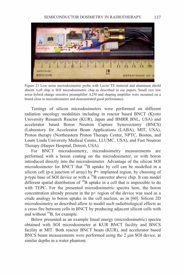
A qualitative comparison between the relative quality of BNCT modalities was made via comparison of microdosimetric spectra and presented on Figs. 22a) and 22b).
In contrast to the KUR results (Fig. 22a) the thermal neutron component (lineal energies greater than 120 keV/ m) is very small in comparison with the proton component for BNCS MIT facility (Fig. 22b). The proton peak originating from nitrogen capture is also absent in Fig. 22b as it is negligible compared to the recoil components. These features reflect the differences in neutron energy spectra of reactor based BNCT and accelerator based BNCS with much higher component of fast neutrons in accelerator based BNCT. It makes difference in biological dose while absorbed dose can be the same. For more details on development and investigation of silicon detectors for microdosimetry in radiation therapy can be found in our publications and papers referred in these publications. [36,65-71].
SEMICONDUCTOR DOSIMETRY IN RADIOTHERAPY 139
Another important application of silicon detectors for microdosimetry is in verification of Monte Carlo simulations in hadron therapy where contribution of elastic and inelastic reaction generating high LET particles in a phantom is due to direct beam interaction. Modeling of the response of silicon microdosimeter by used Monet Carlo transport code followed by experimental verification is a reliable QA for accepting of Monte Carlo based dose planning. Measurements in FNT and proton therapy demonstrated usefulness of this approach [68,74].
(a)
(b)
Figure 22 Microdosimetric spectra obtained under the same condition in a water phantom - a) under mixed mode irradiation at KUR at depth 1cm in water - b) BNCS MIT facility.
6.
Scintillators play an important role in radiation therapy QA. It is a wide area of research with many groups involved. The scope of this paper does not allow detailed discussion of all aspects of the principles and design of such detectors but rather we will be limited to a short discussion of important tools in radiation therapy: Fiber Optical Dosimetry (FOD) and amorphous silicon imaging plate for IMRT and image guided therapy QA.
Application of scintillator based detector in radiation therapy
A.B. ROSENFELD 140
The main principle and advantage of FOD is in tissue equivalency of plastic scintillators, small size and passive mode of application similar to conventional diode dosimetry. The light generated in a scintillator, which is proportional to the dose rate, and delivered through the fiber optic to the photodetector and converted to the readable signal. The main principles of such detectors and dosimetry were firstly described in [75,76]. The main challenge of this detector is a low signal generated in a small volume of plastic scintillator and possible losses of signal on the interface scintillator –FO as well as Cherenkov radiation contribution to the signal related to electrons scattering on a high energy beam of medical LINACs. Essential improvement of light collection by innovative optical coupling of plastic scintillator and FO as well as reduction of Cherenkov radiation effect was achieved recently by University of Sydney group that make this dosimetry suitable for high dose rate application in radiation therapy [77,78].
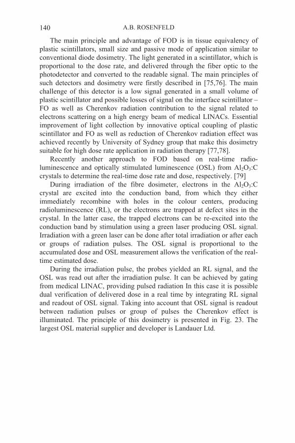
Recently another approach to FOD based on real-time radio-luminescence and optically stimulated luminescence (OSL) from Al2O3:Ccrystals to determine the real-time dose rate and dose, respectively. [79]
During irradiation of the fibre dosimeter, electrons in the Al2O3:Ccrystal are excited into the conduction band, from which they either immediately recombine with holes in the colour centers, producing radioluminescence (RL), or the electrons are trapped at defect sites in the crystal. In the latter case, the trapped electrons can be re-excited into the conduction band by stimulation using a green laser producing OSL signal. Irradiation with a green laser can be done after total irradiation or after each or groups of radiation pulses. The OSL signal is proportional to the accumulated dose and OSL measurement allows the verification of the real-time estimated dose.
During the irradiation pulse, the probes yielded an RL signal, and the OSL was read out after the irradiation pulse. It can be achieved by gating from medical LINAC, providing pulsed radiation In this case it is possible dual verification of delivered dose in a real time by integrating RL signal and readout of OSL signal. Taking into account that OSL signal is readout between radiation pulses or group of pulses the Cherenkov effect is illuminated. The principle of this dosimetry is presented in Fig. 23. The largest OSL material supplier and developer is Landauer Ltd.
SEMICONDUCTOR DOSIMETRY IN RADIOTHERAPY 141
Figure 23 Schematic of the principle of OSL based FOD using Al2O3 OSL material and gated readout system. (Courtesy of Dr Claus E.Andersen, Risø National Laboratory, Denmark).
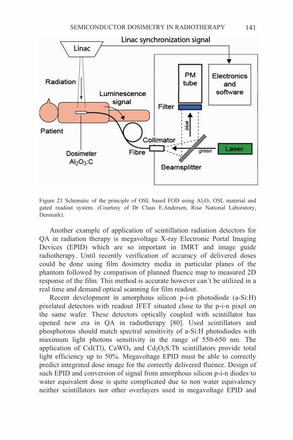
Another example of application of scintillation radiation detectors for QA in radiation therapy is megavoltage X-ray Electronic Portal Imaging Devices (EPID) which are so important in IMRT and image guide radiotherapy. Until recently verification of accuracy of delivered doses could be done using film dosimetry media in particular planes of the phantom followed by comparison of planned fluence map to measured 2D response of the film. This method is accurate however can’t be utilized in a real time and demand optical scanning for film readout.
Recent development in amorphous silicon p-i-n photodiode (a-Si:H) pixelated detectors with readout JFET situated close to the p-i-n pixel on the same wafer. These detectors optically coupled with scintillator has opened new era in QA in radiotherapy [80]. Used scintillators and phosphorous should match spectral sensitivity of a-Si:H photodiodes with maximum light photons sensitivity in the range of 550-650 nm. The application of CsI(Tl), CaWO4 and Cd2O2S:Tb scintillators provide total light efficiency up to 50%. Megavoltage EPID must be able to correctly predict integrated dose image for the correctly delivered fluence. Design of such EPID and conversion of signal from amorphous silicon p-i-n diodes to water equivalent dose is quite complicated due to non water equivalency neither scintillators nor other overlayers used in megavoltage EPID and

A.B. ROSENFELD 142
outside of this paper. Relevant information can be found in [81,82] and references in these papers. Varian EPID and other have a large size and suitable for dosimetry of 40x40 cm radiation field and spatial resolution in dose imaging better then 1mm. Dose measured with ionising chamber in solid water phantom and film and obtained with EPID was in agreement within about 2% [88] that make these new devices extremely efficient in radiation therapy QA. Figure 24 shows 2D dose distribution measured with EPID which in a conjunction with dose planning system able to compare plan and delivered doses in IMRT for any linear scan through the dose image.
Figure 24 Dose image of a intensity modulated radiation therapy beam from a linear accelerator obtained using a commercial (Varian) a-Si electronic portal imaging device. Software allow obtaining on the dose line which can be compared with a planning dose for QA.
SEMICONDUCTOR DOSIMETRY IN RADIOTHERAPY 143
7. Conclusion
Radiation detectors in radiation therapy which is an essential part of radiation medicine are vital for dose verification to guaranty that delivery of radiation to the target is going according to the plan. Semiconductor detectors have many advantages in this application due to their small size, possibility of real time readout, separation of component of mixed radiation fields, biological dosimetry on a cellular level and dose imaging on medical LINACs.
Acknowledgements
I would like to thanks all our collaborators from radiation facilities, radiation oncology in the Australia, USA, Europe and Japan who are contributing essentially to many projects, data from which have been presented in this paper. All of them are coauthors in our publications.
Special thanks to my previous and current PhD students and my colleagues at CMRP who are working with great enthusiasm on many our radiation detection projects and from whom I am constantly learning.
References
1. AAPM “Comprehensive QA for radiation oncology”, Task Group 40, Radiation Therapy Committee, 1993
2. S.M. Zee “Physics of semiconductor devices”, 2nd edition, John Wiley & Sons, 1981 3. J.Shi, W.E. Simon, T.C.Zhu” Modelling the instantaneous dose rate dependence of
radiation diode detectors”, Med.Phys. 30, 2509–2519, 2003 4. D. Marre, G. Marinello, “Comparison of p-type commercial electron diodes for in-vivo
dosimetry”, Med. Phys. 31, 50–56, 2004–06–02 5. P.A. Jursinic, “Implementation of an in-vivo diode dosimetry program and changes in
diode characteristics over 4-years clinical history”, Med. Phys. 28, 1718–1726, 2001 6. A.S. Saini, T.C.Zhu, “Temperature dependence of commercially available diode
detectors”, Med.Phys. 29, 622–630, 2002 7. K.T. Welsh, L.E. Reinstein, “The thermal characteristics of different diodes on in-vivo
patient dosimetry”, Med.Phys. 28, 844–849, 2001 8.
quality assurance in IMRT”, Med. Phys. 30, 3118–3123, 2003 9. P.A. Jursinic, B.E. Nelms, “A 2-D diode array and analysis software for verification of
intensity modulated radiation therapy delivery”, Med.Phys. 30, 870–879, 2003 10. C.D. Angelis, S. Onori,M.Pacilio, G.A.P. Cirone, G. Cuttone, L. Raffaele, M.
Bucciolini, S. Mazzocchi, “An investigation of the operating characteristics of two PTW diamond detectors in photonand electron beams”, Med. Phys. 29, 248–254, 2002
11. M. Bucciolini, F.B. Buonamici, S. Mazzocchi, C.D. Angelis, S. Onori, G.A.P. Cirrone, “Diamond detector versus silicon diode and ion chamber in photon beams of different energy and field size”, Med.Phys. 30, 2149–2154, 2003
P.D. Hoggins, P. Alaei, B.J. Gerbi, K.E. Dusenbery, “In-vivo diode dosimetry for routine
A.B. ROSENFELD 144
12. Holmes-Siedle, “The Space Charge Dosimeter”, Nucl. Inst. Meth, 121, 169–179, (1974) 13. Freeman, R., Holmes-Siedle, A., A Simple Model for Predicting Radiation Effects in
MOS Devices, IEEE Trans. Nucl. Sci., NS-25–6, 1216–1225, (1978) 14. Butson, M.J., Rozenfeld, A.B., Mathur, J.N., Carolan, M., Wong, T.P., Metcalfe, P.E., A
New Radiotherapy Surface Dose Detector: The MOSFET, Med. Phys., 23–5, 655–658,(1996)
15. Rosenfeld, A.B., Carolan, M.G., Allen, B.J., et al, MOSFET Dosimeters: role of encapsulation in mixed gamma-neutron and megavoltage X-ray fields, IEEE Trans. on
Nucl. Sci., NS-42, N6, 1870–1877, (1995) 16. Ramani, R., Russell, S., O'Brien, P., Clinical Dosimetry using MOSFETs, Int. J.
Radiation Oncology Biol. Phys., 37–4, 959–964, (1997) 17. Quach, K.Y., Morales, J., Butson, M.J., Rosenfeld, A.B., Metcalfe, P.E., Measurements
of Radiotherapy X-ray Skin Dose on a Chest Wall Phantom, Med. Phys., 27–7, 1676–1680, (2000)
18. Cheung, T., Butson, M.J., Yu, P.K.N. “Effect of temperature variation on MOSFET dosimetry”, Phys. Med.Biol., 49, 191–196, 2004
gamma and proton dosimetry", Rad. Prot. Dos.33, N1/4, 179–182, 1990 20. Soubra, M., Cygler, J., Mackay, G., Evaluation of a Dual bias Dual Metal Oxide-Silicon
Semiconductor Field Transistor Detector as Radiation Dosimeter, Med. Phys., 21–4, 567–572, 1994
21. Rosenfeld, A.B., Kaplan, G.I., Allen, B.A., Dilmanian, A., Kron, T., Holmes-Siedle, A., MOSFET Dosimetry of X-ray Microbeams, IEEE Trans. on Nucl Sci., NS-46, N6, 1774–1780, (1999)
22. Kaplan, G., Rosenfeld, A., Allen, B., Booth, J., Carolan, M. and Holmes-Seidle, A. Improved spatial resolution by MOSFET dosimetry of an x-ray microbeam Med. Phys. 27, 239–244, (2000)
MOSFET detectors”, Rad.Prot.Dos., 101, N1/4, 445–448, 200224. LoSasso, T., Chui, C. and Ling, C. Physical and dosimetric aspects of a multileaf
collimation system used in the dynamic mode for implementing intensity modulated radiotherapy. Med. Phys. 25, 1919–1927 (1998)
25. D.N. Slatkin et al. “Microbeam radiation therapy”, Med.Phys, 19, 1395–1400, 1992 26. J.A. Laissue at al. “Neuropathology of ablation of rat gliosarcomas and contiguous brain
tissue using a microplanar beam of synchrotron-wiggler-generated X-rays”, Int.J.Cancer, 78, 654–660, 1998
27. Orion, I., Rosenfeld, A.B., Dilmanian, A., Telang, F., Ren, B., Namito, Y., Monte Carlo Simulations of Dose Distribution from a Synchrotron-Produced Micro-planar Beam Array using the EGS4 Code System, Med. Phys. Biol., 45, 2497–2508, (2000)
28. Rosenfeld, A.B., Lerch, M.L.F., et al, Feasibility Study of On-line, High Spatial Resolution MOSFET Dosimetry in Static and Pulsed X-ray Radiation Fields, IEEE Trans. Nucl. Sci., NS-48-N6, (2001)
Laissue “MOSFET dosimetry for Microbeam radiation therapy at the European Synchrotron Radiation Facility”, Med.Phys., 31(3), 609–615, 2004.
30. Rosenfeld, A.B., Erik A. Siegbahn, Elke Brauer-Krish, Andrew Holmes-Siedle, Michael L.F. Lerch, Alberto Bravin, Iwan M. Cornelius, George J. Takacs, Nirmal Painuly, Heidi Nettelback, Tomas Kron “Edge on Face-to-Face (EOFF) MOSFET for Synchrotron Microbeam Dosimetry: MC modeling”, IEEE Trans on Nucl. Sci., NS-52, N6, December, 2005
19. P.G. Litovchenko, L.I. Barabash, A.B. Rosenfeld et. al. "MOS structure for emergency
23. T. Kron, A. Rosenfeld, M. Lerch, “Measurements in radiotherapy beams using on-line
29. E. Brauer-Krish, A. Bravin, M. Lerch, A. Rosenfeld, J. Stepanek, M. Di. Michiel, J.A.
SEMICONDUCTOR DOSIMETRY IN RADIOTHERAPY 145
31 Seigbahn, E.A., Brauer-Krisch, E., Stepanek, J., Blattman, H., Laissue, J.A., Bravin, A., Dosimetric studies of microbeam radiation therapy (MRT) with Monte Carlo simulations., Nucl. Instr. Meth. In Phys. Res. A, 2005
32. E. Brauer-Krischa, H. Requardta, P. Régnarda, S. Cordea, E. Siegbahna, G. LeDuca, T. Brocharda, H. Blattmannb, J. Laissuec, A. Bravina, New irradiation geometry for Microbeam Radiation Thearpy (MRT), Nucl. Instr. Meth, 2005
33. Butson, M., Cheung, T., Yu, P.K.N., Peripheral dose measurement with a MOSFET detector., Applied Radiation and Isotopes, 62, 631–634, 2005
34. Rosenfeld, A.B. (invited paper) “MOSFET dosimetry in modern radiation oncology modalities”, Rad. Prot.Dosim, 101, N1/4, 393–398, 2002
35. Kaplan, G.I., Rosenfeld, A.B., Allen, B.J., Coderre, T.A., Liu, H.B., Fission Converter and MOSFET Study of Thermal Neutron Flux Distribution in an Epithermal Neutron Therapy Beam, Med. Phys., 26–9, 1989–1994, (1999)
36. Rosenfeld, A., Kaplan, G., Carolan, M., B. Allen, Maughan, R., Yudelev, M., Cota, C., and. Coderre, J., “Simultaneous Macro and Micro Dosimetry with MOSFETs,” IEEE Trans. Nucl. Sci., vol. 43, pp. 2693–2700, 1996
37. J.M. Swartz, M.O. Thurston, “Analysis of the effect of fast-neutron bombardment on the current-voltage characteristics of a conductivity modulated p-i-n diode”, J. Appl. Phys. Vol. 37 (2), pp 745–755, 1966
38. A.B. Rosenfeld, I.E. Anokhin, L.I. Barabash, O.S. Zinets, P.G. Litovchenko, V.I. Khivrich, L.F. Belovodskiy, A.I. Dumik, V.I. Fominych, V.I. Petrov, G.F. Sluchenkov and G.N. Koval, “P-I-N diodes with a wide measurements range of fast neutron doses”, Rad. Protect. Dosim. 33, 175–178, 1990
39. I.E. Anokhin, A.B. Rosenfeld, O.S. Zinets, "Evolution of radiation induced defects and the type inversion in high receptivity silicon under neutron irradiation", Rad Prot Dos,101, N1/4, 107–110, 2002
40. Khivrich, V.I. Varentsov, M.D. Litovchenko, P.G. Anokhin, A.I. Zinets, O.S. Reinhard, M.I. Rosenfeld, A.B. Carolan, M. Alexiev, D., "High purity silicon as a basic material for manufacturing of radiation detectors and integral neutron dosimeters”, IEEE Trans. on Nucl. Sci. 43, N6, 2687–2692, 1996
41. Reft, C.S., Kuchnir, F.T., Awschalom, M. and Lennox, A. Neutron dosimetry with silicon diodes. Med. Phys. 13 (4), 578 (1986)
42. A.B. Rosenfeld, M. Yudelev, M. Lerch, I. Cornelius, P. Grifin, V. Perevertaylo, I.E Anokhin, O.S. Zinets, V.I. Khivrich, M. Pinkovskaya, D. Alexiev, M. Reinhard. “New neutron dosimetry with planar silicon PIN diodes”, IEEE Trans. Nucl. Sci., NS-50, N6, 2367–2372, 2003
43. Maughan, R.L. and Yudelev, M. Physical characteristics of a clinical d (48.5) +Be neutron therapy beam produced by a superconducting cyclotron. Med. Phys. 22 (9), 1459–1465 (1995)
44. Maughan, R.L., Yudelev, M. and Kota, C.A measurement of the fast-neutron sensitivity of a Geiger-Muller detector in the pulsed neutron beam from a superconducting cyclotron. Phys. Med. Biol. 41 (4), 1341–1351 (1996)
45. A. Rosenfeld, G. Kaplan, M. Carolan, B. Allen, O. Zinets, V. Khivrich, P.G. Litovchenko “Application of P-I-N diodes and MOSFET for dosimeter in gamma and neutron fields”, Rad.Prot.Dosim., 84, N1–4, 349–352, 1999
46. M. Yudelev, K. Alyosef, J. Brandon, V. Perevertailo, M.L.F. Lerch, A.B. Rosenfeld “Application of semiconductors for dosimetry of fast-neutron therapy beam”, Rad.Prot.Dosim., 110, N1–4, 573–578, 2004
A.B. ROSENFELD 146
47. K. Alyousef “Use of miniature semiconductor dosimeters in mixed neutron/gamma beam”, PhD thesis, Wayne State University, School of Medicine, 2005. (Supervisors Dr M. Yudelev and Prof. A. Rosenfeld)
48. A.B. Rosenfeld, K. Alyousef, M. Yudelev, J. Brandon, V. Perevertailo, M. L. F.
49. G. Kaplan, A.B. Rosenfeld, B. Allen, J.A. Coderre, H.B. Liu, “Fission converter and MOSFET study of thermal neutron flux distribution in an epithermal neutron therapy
50. G.I. Kaplan “Integral and pulse mode silicon dosimetry for dose verification on radiation oncology modalities”, PhD Thesis, University of Wollongong, 2001, Australia (Supervisor Prof.A.B. Rosenfeld)
51. thermal neutron si detector probe in BNCT 52. Torru Kabayshi, KRR, Japan, private communication 53. H.H. Rossi and W. Rosenzweig, “A device for the measurement of dose as a function of
specific ionization,” Radiology, vol. 64, pp. 404–411, 195554. International Commission on Radiation Units and Measurements, Microdosimetry,
ICRU Report N 36, 198355. H.H. Rossi and M.Zaider, “Microdosimetry and Its Applications”, London: Springer,
199656. P. Bradley, A. Rosenfeld “Tissue equivalent Correction for Silicon Microdosimetry
57. P. Bradley, A.B. Rosenfeld, K.K. Lee, D. Jamieson, S. Satoh "Charge collection and radiation hardness of a SOI microdosimeter for space and medical application", IEEE
Trans on Nucl Sci, NS-45, N6, 199858. P. Bradley, A.B. Rosenfeld, B.J. Allen, J. Coderre, J. Capela "Performance of silicon
microdosimetry detectors in boron neutron capture therapy", Radiation Research, 151,235–243, 1998
59. A. Rosenfeld, P. Bradley, I. Cornelius, J. Flanz “New silicon detector for microdosimetry applications in proton therapy”, IEEE Trans on Nucl.Sci., 47, N4, 1386–1394, 2000
60. A.B. Rosenfeld, P. Bradley, “Semiconductor microdosimetry in mixed radiation and photon fields: present and future”, Rad.Prot. Dosim., 85, N 1–4, 385–388, 1999
61. I. Cornelius, A.B. Rosenfeld, P.D. Bradley “Computational technique for deposition energy in complicated silicon structures”, IEEE Trans. Nucl, Sci, 47, N6, 2423–2427, 2000
62. P.D. Bradley, A.B. Rosenfeld, B.J. Allen, et al. “Application of Silicon diode arrays for microdosimetry in BNCT and FNT”, in a book Frontiers in Neutron Capture Therapy, p.615–622, edited by Hawthrone at al., Kluwer Academic/Plenum Publisher, 2001
101,N1/4, 431–434, 2002
64. I. Cornelius, A. Rosenfeld, R. Siegele, D. Cohen, “IBIS characterization of silicon microdsimeters for space and medical application using a heavy ion microprobe”,
Nucl.Instr. Meth. in Physics Research B, 19, 335–338, 200165. I. Cornelius, A. Rosenfeld, Rainer Siegele, David Cohen “Improvement of SOI
microdosimeter performance by using pulse shape discrimination technique”, IEEE
fields”, IEEE Trans. on Nucl. Sci., (to be published)
beam”, Med.Phys., 26(9), 1989–1994, 1999
Lerch, “Single sensors for separate neutron and gamma dosimetry in mixed radiation
detectors in Boron Neutron Capture therapy”, Med.Phys., 25(11), 2220–2225, 1998
63. A.B. Rosenfeld, P.D. Bradley, I. Cornelius, M. Zaider, R. Maughan, J. Flanz, J. Yanch,
Trans. Nucl. Sci, 49, N6, 2805–2809, 2002.
T. Kobayashi, B.J. Allen. “Microdosimetry in hadron therapy”, Rad.Prot.Dosim.
SEMICONDUCTOR DOSIMETRY IN RADIOTHERAPY 147
66. Iwan Cornelius, Anatoly Rosenfeld, Peter Bradley “Simulation of silicon microdosimetry measurements in fast neutron therapy”, Australas. Phys. Eng. Sci. Med.,26, N4, 168–171, 2002
67. I.M. Cornelius, A.B. Rosenfeld, R. Seigele, D. Cohen, “Charge collection in microdosimeter on heavy ions” IEEE Trans. On Nucl. Sci, 50, 2373–2379, 2003
68. I. Cornelius, A. Rosenfeld “Monte Carlo verification in Fast Neutron Therapy”, IEEE
Trans. on Nucl. Sci, 51, N3, 873–877, 2004 69. A. Wroe, A. Rosenfeld, I. Cornelius, D. Prokopovich, M. Reinhard, R. Schulte, V.
Bashkirov “Microdosimetric spectra within heterogeneous tissue equivalent structures”, IEEE Trans on Nucl. Sci, 2006, (to be published)
70. P.D. Bradley, PhD thesis “Development of novel silicon microdosimeter for high LET radiation therapy”, University of Wollongong, Australia (2000), supervisor Prof. A.B. Rosenfeld.
71. I.M. Cornelius, PhD Thesis “Towards silicon microdosimetry based verification of Monte Carlocalculations in hadron therapy” University of Wollongong, Australia (2004), supervisor Prof A.B.Rosenfeld.
72. A.B. Rosenfeld, A. Wroe, I. Cornelius, M. Carolan “Verification of Monte Carlo simulations in radiation therapy” Rad. Prot. Dosim. 2006, (in press)
73. Beddar, A.S., Mackie T.R., Attix F.H., Watter-Equivalent plastic scintillation detectors for high –energy beam dosimetry: Part I, Physical characteristics and theoretical consideration, Phys. Med.Biol. 37, 1883–1900, 1992
74. Beddar, A.S., Mackie T.R., Attix F.H., Watter-Equivalent plastic scintillation detectors for high –energy beam dosimetry: Part II Properties and measurements, Phys. Med. Biol. 37, 1901–1913, 1992
75. Beddar, A.S., Law, S., Suchowerska, N., Mackie T.R., Plastic scintillation dosimetry:optimization of light collection efficiency, Phys.Med. Biol., 48, N9, 1141–1152, 2003
76. Beddar A.S., Suchowerska N., Law, S., Plastic scintillation dosimetry for radiation therapy: minimizing capture of Cherenkov radiation noise, Phys.Med. Biol., 49, 2004
77. C.J. Marckmann, C.E. Andersen, M.C. Aznar, and L. Bøtter-Jensen, Optical fibre dosemeter systems for clinical applications based on radioluminiscent\ce and optically stimulated luminescence from Al2O3:C., Rad. Prot. Dosim., 2006 (in press), and private communication.
78. L.E. Antonuk, J. Bourdy, W. Huang, D.L. McShan, E.J. Morton, J. Yorkston, M.J. Longo, R.A. Street “Demonstartion of megavoltage and diagnostic x-ray imaging with hydrogenated amorphous silicon arrays”, Med.Phys. 19 (6), 1455–1465, 1992
79. B. Warkentin, S. Steciw, S. Rathee, B.G. Fallone “Dosimetric IMRT verification with a flat panel EPID”, Med. Phys., 30(12), 3143–3155, 2003
80. Peter B. Greer, Carmen C. Popescu “Dosimetric properties of an amorphous silicon electronics portal imaging device for verification of dynamic intensity modulated radiation therapy”, Med.Phys. 30(7), 1618–1627, 2003