semiconductor plate interacting with te mode in … · semiconductor plate interacting with te01...
TRANSCRIPT

Lithuanian Journal of Physics, Vol. 49, No. 1, pp. 35–43 (2009) doi:10.3952/lithjphys.49116
SEMICONDUCTOR PLATE INTERACTING WITH TE01 MODE INCIRCULAR WAVEGUIDE
Ž. Kancleris, G. Šlekas, V. Tamošiunas, R. Simniškis, P. Ragulis, and M. TamošiunieneSemiconductor Physics Institute, A. Goštauto 11, LT-01108 Vilnius, Lithuania
E-mail: [email protected]
Received 24 December 2008; revised 20 February 2009; accepted 19 March 2009
In this paper, the possibility to use the semiconductor obstacle placed on the wall of the circular waveguide as the resistivesensor is analysed. The simplified model of the semiconductor obstacle is considered and the method to solve Maxwell’sequations in the cylindrical coordinate system is presented for TE01 mode, which is most suitable for the transmission ofhigh power signals. The finite-difference time-domain method was employed for the calculation of the electromagnetic fieldcomponents in cylindrical waveguide, reflection coefficient from the semiconductor obstacle, and the average electric field init. Computation results were tested by comparing computed results with the analytical solution.
Keywords: electromagnetic wave, TE01 mode, circular waveguide, semiconductor obstacle, resistive sensor
PACS: 41.20.-q, 07.50.-e
1. Introduction
Since the TE01 mode propagating in a circularwaveguide is a low loss mode, it is often used for thedesign of microwave devices. The currents associatedwith TE01 modes are in the circumferential directiononly and this property may be of some use to constructmode filters that suppress modes having currents di-rected along the waveguide axis [1]. The propertiesof TE01 mode mentioned above have been applied in[2–6].
The gyrotron-backward-wave-oscillator (gyro-BWO)experiments, which utilize a high-current (1–4 kA) anda high-voltage (300–500 keV) annular electron beam,were presented in [2]. The designed gyro-BWO oper-ated in the TE01 backward wave mode, extracted powerwas 0.1–0.4 MW and cutoff frequency was approxi-mately 4.2 GHz.
In [3], a design for circular waveguide bends propa-gating the low loss TE01 mode was considered. The de-tailed design of the bend and the comparison of simula-tion results with experimental data were presented. Thebend has smooth walls and very low ohmic losses. TheTE01 mode is transmitted with virtually perfect modepurity.
The theory for a single-time-switched resonant de-lay line pulse compression system has been developedin [4]. The switch operating in TE01 mode in a circular
waveguide avoiding the edge effects at the interface be-tween the silicon wafer and the supporting waveguidewas proposed. A design example for an active iris op-erating in TE01 mode has been presented.
The design and test of a 100 MW-band TE01 win-dow was presented in [5]. A TE01 nonreciprocal phaseshifter in a 50 MW test bench has been tested in [6].
The overview presented above confirms that circu-lar waveguides operating at TE01 mode have been reg-ularly used in high power microwave (HPM) experi-ments. In the present paper we have investigated theinteraction of a semiconductor plate inserted into a cir-cular waveguide with the TE01 mode propagating init. We have solved Maxwell’s equations using finite-difference time-domain (FDTD) method in a cylindri-cal coordinate system. The object of our investigation –the semiconductor plate – might be considered as a pro-totype of a resistive sensor (RS) [7]. The performanceof it is based on electron heating effect and the RSis used for direct measurement of HPM pulses in thetransmission lines and free space. The resistive sen-sors developed for rectangular waveguides are used inlaboratories dealing with HPM pulses worldwide. Un-fortunately, the RS for the circular waveguide has notbeen designed yet.
c© Lithuanian Physical Society, 2009c© Lithuanian Academy of Sciences, 2009 ISSN 1648-8504

36 Ž. Kancleris et al. / Lithuanian J. Phys. 49, 35–43 (2009)
Fig. 1. The view of lines of the electromagnetic field in a circular waveguide for mode TE01.
2. Electromagnetic field components
Although the TE01 mode is the simplest TE mode inthe circular waveguide, it is not the lowest one. Thecritical frequency of the TE01 mode in a waveguideis twice that of the lowest TE11.The view of lines ofthe electromagnetic field in the circular waveguide formode TE01 is presented in Fig. 1. The regular wavehas only three components: Eϕ, Hr, and Hz . They areindependent of the azimuthal angle ϕ. Dependences ofthe amplitudes of the regular wave on the radial r andaxial z coordinates can be expressed in the followingway [8]:
Eϕ(r, z) = A J1
(
µ01r
a
)
exp
(
−i2πz
λw
)
, (1)
Hr(r, z) =−Aλ
λw
√
ε0
µ0
J1
(
µ01r
a
)
exp
(
−i2πz
λw
)
,
(2)
Hz(r, z) = jAλ
λc
√
ε0
µ0
J0
(
µ01r
a
)
exp
(
−i2πz
λw
)
.
(3)
Here the coefficient A is measured in electric fieldunits and depends on the power propagating throughthe waveguide, λ, λw, and λc are the wavelength ofelectromagnetic oscillations in free space, in a wave-guide, and the critical wavelength for the TE01 mode,respectively, ε0 and µ0 are the vacuum permittivity andpermeability, J0 and J1 are the corresponding orderfirst kind Bessel functions, µ01 = 3.832 is the rootof J1: J1(µ01) = 0, and a is the radius of the wave-guide. In the interval 0–µ01 Bessel function J1 reachesits maximum at µ11 = 1.841, where µ11 is the root ofthe first derivative of J1. Therefore, the maximum ofthe components Eϕ and Hr in the radial direction isalmost halfway between the centre and the wall of thewaveguide (r/a = µ11/µ01 = 0.4804).
Fig. 2. A plate of the semiconductor with metal contacts on the wallof the circular waveguide: (a) contacts on the top and bottom sur-faces – vertical configuration, (b) contacts on the sidewalls – hori-zontal configuration, and the practical realization of the (c) verticaland (d) horizontal configurations in the circular waveguide using
plane samples.
The critical wavelength for the TE01 mode λc =
1.640a [8], and the wavelength in the waveguide is ex-pressed as
λw =λ
√
1 − (λ/λc)2. (4)
The power transfer by the TE01 mode can bystraightforwardly computed by integrating the Pointingvector over cross-sectional area of the waveguide.

Ž. Kancleris et al. / Lithuanian J. Phys. 49, 35–43 (2009) 37
Fig. 3. Sectional view of the modelled circular waveguide with obstacle in (a) x0z plane and (b) x0y plane.
3. Layout of the sensing element
As already mentioned in Introduction, the perfor-mance of the RS is based on electron heating effectin semiconductors. Thus, the sensing element (SE) isactually a resistor made of n-type Si with two ohmiccontacts. An electric field of electromagnetic waveheats electrons in the SE, its resistance increases, andby measuring this resistance change the pulse power ofelectromagnetic wave in the waveguide is determined[7]. Therefore, any plate inserted in the waveguidewith properly arranged contacts could serve as a SE.Depending on the position of the metal contact on theplate, we propose two configurations shown in Fig. 2.We named “vertical” the plate with the contacts onits top and bottom, shown in Fig. 2(a), while a platewith the contacts on sidewalls was named “horizontal”(Fig. 2(b)). These two names will be used further with-out quotes to denote the particular configuration of theSE.
The possible practical realization of the vertical de-sign using plane samples is shown in Fig. 2(c). It isseen that the proposed RS consists of two separate SEsplaced in a close proximity to each other. Their topcontacts are shorted with a thin metal foil. The bottomcontact of one of the SEs is grounded while the otherone is isolated from the waveguide and is used for theRS feeding and the output signal measurement. Actu-ally, the sensing elements are connected in series withrespect to the DC current but in parallel with respect tothe microwave electric field.
The realization of the horizontal configuration is de-picted in Fig. 2(d). It is seen that the plane SE is simplylaid on the isolating dielectric on the wall of the wave-guide. One of contacts of the SE is grounded, while theother one is isolated from the waveguide and is used forthe RS feeding and the output signal measurement.
Comparing the vertical and horizontal configura-tions it can be concluded that, on the one hand, thevertical configuration can be simpler realized using thesoldering technique for mounting of samples in thewaveguide. It will not be the case for the horizontalconfiguration where the SE should be isolated from thewall of the waveguide. On the other hand, horizon-tal configuration might be more acceptable from theviewpoint of homogeneity of the electric field in theSE since the metal contacts are perpendicular to the di-rection of the electric field Eϕ in the regular wave. Inthe vertical configuration, the contacts in general areparallel to the Eϕ, therefore the regular component iszeroed by the contact surface.
4. FDTD method
For the calculation of electromagnetic field compo-nents in the waveguide with semiconductor obstacle wehave used FDTD method [9, 10], application of whichfor cylindrical coordinate system will be given below.
The modelled section of the waveguide with the ob-stacle is shown in Fig. 3. We used a cylindrical coor-dinate system and dimensionless coordinates and time:r/a, ϕ, z/a, t v/a, where v is the velocity of light infree space and a is a radius of the waveguide. In theplane z = zex, the TE01 type wave is excited. It prop-agates into both sides from the excitation plane. Theobstacle is placed at one wavelength in the waveguideahead from the excitation plane and at the same dis-tance before the right side of the modelled waveguidesection. In the planes z = 0 and z = zmax nonre-flecting boundary conditions are satisfied. Therefore,the waves travelling left from the excitation plane aswell as reflected from the semiconductor obstacle areabsorbed in the plane z = 0, whereas the wave pass-ing semiconductor structure is absorbed in the plane

38 Ž. Kancleris et al. / Lithuanian J. Phys. 49, 35–43 (2009)
z = zmax. Due to the reflection from the semiconduc-tor obstacle a partly standing wave is formed betweenplanes z = zex and z = zob. From the amplitude dis-tribution in this area, the reflection coefficient was de-termined.
Although the regular TE01 type wave has one elec-tric field component Eϕ and two magnetic field compo-nents Hr and Hz (Eqs. (2) and (3)), in the vicinity of theSE all electromagnetic field components might appear.Therefore, to determine the average electric field am-plitude in the semiconductor obstacle Maxwell’s equa-tions have to be solved computing all six componentsof the electric and magnetic fields. Making use ofdimensionless variables and expressing the magneticfield strength in electric field units Z0H , where Z0 isan impedance of free space, Maxwell’s equations inthe semiconductor obstacle can be written down in afollowing way:
∂E
∂t=
∇× H − γE
ε, (5)
∂H
∂t=−∇× E , (6)
where γ = Z0a/ρ accounts for losses in the structure.Here ρ and ε are the specific resistance and relative di-electric constant of the semiconductor obstacle and itis assumed that µ = 1 for the entire simulation area.Outside the semiconductor obstacle γ = 0 and ε = 1.
Making use of cylindrical coordinates for the calcu-lation of the curl of the electric and magnetic field andreplacing time and coordinate derivatives in (5) and (6)with finite differences, one can obtain the following setof equations for updating new values of the componentsfrom the older ones:
Hr
∣
∣
∣
n+1
2
i,j+ 1
2,k+
1
2
= Hr
∣
∣
∣
n− 1
2
i,j+ 1
2,k+
1
2
+∆t
∆z
×
(
Eϕ
∣
∣
∣
n
i,j+ 1
2,k+1
− Eϕ
∣
∣
∣
n
i,j+ 1
2,k
)
−∆t
i∆ϕ∆r
×
(
Ez
∣
∣
∣
n
i,j+1,k+1
2
− Ez
∣
∣
∣
n
i,j,k+1
2
)
, (7)
Hϕ
∣
∣
∣
n+1
2
i+ 1
2,j,k+
1
2
= Hϕ
∣
∣
∣
n− 1
2
i+ 1
2,j,k+
1
2
+∆t
∆r
×
(
Ez
∣
∣
∣
n
i+1,j,k+1
2
− Ez
∣
∣
∣
n
i,j,k+1
2
)
−∆t
∆z
×
(
Er
∣
∣
∣
n
i+ 1
2,j,k+1
− Er
∣
∣
∣
n
i+ 1
2,j,k
)
, (8)
Hz
∣
∣
∣
n+1
2
i+ 1
2,j+ 1
2,k
= Hz
∣
∣
∣
n− 1
2
i+ 1
2,j+ 1
2,k
+∆t
(i + 1
2)∆r∆ϕ
×
(
Er
∣
∣
∣
n
i+ 1
2,j+1,k
− Er
∣
∣
∣
n
i+ 1
2,j,k
)
−∆t
(i + 1
2)∆r
×
(
(i + 1)Eϕ
∣
∣
∣
n
i+1,j+ 1
2,k− iEϕ
∣
∣
∣
n
i,j+ 1
2,k
)
, (9)
Er
∣
∣
∣
n+1
i+ 1
2,j,k
= Er
∣
∣
∣
n
i+ 1
2,j,k
+1
ε
− γEr
∣
∣
∣
n
i+ 1
2,j,k
+
+∆t
(i + 1
2)∆r∆ϕ
(
Hz
∣
∣
∣
n+1
2
i+ 1
2,j+ 1
2,k−Hz
∣
∣
∣
n+1
2
i+ 1
2,j− 1
2,k
)
−∆t
∆z
(
Hϕ
∣
∣
∣
n+1
2
i+ 1
2,j,k+
1
2
− Hϕ
∣
∣
∣
n+1
2
i+ 1
2,j,k− 1
2
)
, (10)
Eϕ
∣
∣
∣
n+1
i,j+ 1
2,k
= Eϕ
∣
∣
∣
n
i,j+ 1
2,k
+1
ε
− γEϕ
∣
∣
∣
n
i,j+ 1
2,k
+
+∆t
∆z
(
Hr
∣
∣
∣
n+1
2
i,j+ 1
2,k+
1
2
− Hr
∣
∣
∣
n+1
2
i,j+ 1
2,k− 1
2
)
−∆t
∆r
(
Hz
∣
∣
∣
n+1
2
i+ 1
2,j+ 1
2,k− Hz
∣
∣
∣
n+1
2
i− 1
2,j+ 1
2,k
)
, (11)
Ez
∣
∣
∣
n+1
i,j,k+1
2
= Ez
∣
∣
∣
n
i,j,k+1
2
+1
ε
− γEz
∣
∣
∣
n
i,j,k+1
2
+∆t
i∆r
×
(
(i +1
2)Hϕ
∣
∣
∣
n+1
2
i+ 1
2,j,k+
1
2
−(i −1
2)Hϕ
∣
∣
∣
n+1
2
i− 1
2,j,k+
1
2
)
−∆t
i∆ϕ∆r
(
Hr
∣
∣
∣
n+1
2
i,j+ 1
2,k+
1
2
−Hr
∣
∣
∣
n+1
2
i,j− 1
2,k+
1
2
)
. (12)
In (7)–(12) ∆t, ∆r, ∆ϕ, and ∆z are time and cylin-drical coordinate steps, lower indexes i, j, and k standfor r, ϕ , and z. The upper index n denotes the numberof a time step. The grid of points where the particu-lar component is computed is shifted at a half of stepwith respect to each other as it has been proposed byYee [9]. Moreover, electric and magnetic fields are cal-culated at different time moments providing h2 accu-racy in the calculation of both space and time deriva-tives. The details of the application of this technique

Ž. Kancleris et al. / Lithuanian J. Phys. 49, 35–43 (2009) 39
to the cylindrical coordinate system can be found inthe monograph [10]. The grid can be chosen in such away that it starts and finishes with the points where theelectric field components should be calculated. For theinvestigated frequency range real metals can be suffi-ciently precisely simulated using so-called perfect elec-tric conductor approximation, which assumes that tan-gential electric field components are simply zeroed onthe metal surface. Therefore, the components Eϕ andEz are zeroed on the waveguide walls. Also, the gridhas been chosen in such a way that tangential electro-magnetic field components were located in the contactplane and consequently were zeroed during FDTD up-date. Depending on the considered configuration ofthe SE, corresponding components of the electric fieldare set to zero on the metal contacts: Eϕ and Ez forthe vertical configuration, Er and Ez for the horizontalone. In the planes z = 0 and z = zmax nonreflectingboundary conditions for the components Er and Eϕ aresatisfied.
At t ≤ 0 there are no electromagnetic fields in themodelled section of the waveguide, therefore all com-ponents of the electric and magnetic field are set tozero. When the dimensions of the semiconductor ob-stacle are much less than the characteristic dimensionsof the waveguide, its influence on the wave propagat-ing in the waveguide is comparatively small. In such acase, by filling the waveguide with the ordinary TE01
wave components, the stationary solution is achievedfaster.
In choosing the time step, the Courant criterion for-mulated for 3D cylindrical coordinate FDTD procedurein [11] has to be taken into account. Considering thewaveguide with the obstacle in an x0y (Fig. 3(b)) planeand having in mind that components of the regularTE01 wave are independent of ϕ, one can see that thedistribution of electromagnetic field amplitudes shouldbe symmetrical with respect to the x0z plane. There-fore, saving the computer memory only a half of thewaveguide window is modelled.
Considering expressions for updating components ofthe electromagnetic field (7)–(12) it is seen that someof them, namely Hr (7), Eϕ (11), and Ez (12) cannotbe straightforwardly computed at i = 0 (r = 0). Thisfact is known as the numerical singularity of a FDTDscheme in cylindrical coordinates at r = 0 [10]. Avariety of numerical procedures dealing with the sin-gularity has been proposed. More widely an integralform of Maxwell’s equations near r = 0 [12, 13] andthe series polynomial expansion in the radial direction[14, 15] have been used to resolve the problem. We
have followed the simple method proposed in [16] andbased on the use of the Cartesian coordinate system inthe vicinity of r = 0 leading to the following expres-sions for calculation of the components at i = 0:
Hr
∣
∣
∣
n+1
2
0,j+ 1
2,k+
1
2
=
(
Hϕ
∣
∣
∣
n+1
2
1
2,0,k+
1
2
−Hϕ
∣
∣
∣
n+1
2
1
2,π,k+
1
2
)sin ϕj+ 1
2
2
+
(
Hϕ
∣
∣
∣
n+1
2
1
2, 3π
2,k+
1
2
− Hϕ
∣
∣
∣
n+1
2
1
2, π
2,k+
1
2
)cos ϕj+ 1
2
2, (13)
Ez
∣
∣
∣
n+1
0,j,k+1
2
= Ez
∣
∣
∣
n
0,j,k+1
2
+∆t
∆r
(
Hϕ
∣
∣
∣
n+1
2
1
2,0,k+
1
2
+Hϕ
∣
∣
∣
n+1
2
1
2, π
2,k+
1
2
+Hϕ
∣
∣
∣
n+1
2
1
2,π,k+
1
2
+Hϕ
∣
∣
∣
n+1
2
1
2, 3π
2,k+
1
2
)
, (14)
Eϕ
∣
∣
∣
n+1
0,j+ 1
2,k
=
(
Er
∣
∣
∣
n+1
1
2,π,k
− Er
∣
∣
∣
n+1
1
2,0,k
)sin ϕj+ 1
2
2
+
(
Er
∣
∣
∣
n+1
1
2, π
2,k− Er
∣
∣
∣
n+1
1
2, 3π
2,k
)cos ϕj+ 1
2
2, (15)
where ϕj+ 1
2
= (j + 1
2) ∆ϕ. The second index in Hϕ
and Eϕ is formal, denoting the values of the componenton the x or y axis. Thus, the components Hr, Ez , andEϕ at r = 0 can be straightforwardly computed using(13), (14), and (15). The only restriction is imposedon the azymuthal step ∆ϕ size. It should be chosen asπ/(2n), where n = 1, 2, . . . .
5. The program
The program computing the electromagnetic fieldcomponents was written using C++ programming lan-guage. It works as follows. During calculations theamplitudes of the particular component of the electro-magnetic field at each point of the investigated structureare summed and stored in additional arrays. After eachperiod, the amplitudes of the component Eϕ are cal-culated. The values of Eϕ for j = 1
2and each i and k
are compared with the values calculated one period ear-lier. The calculations are terminated when the largestdifference between these values is less than the prede-termined value δ. Otherwise, the successive period ismodelled. The number of periods that are necessaryto model depends on the obstacle size and specific re-sistance. For small obstacles, the difference betweenamplitudes less than 0.01 can be achieved after 3 peri-ods.
40 Ž. Kancleris et al. / Lithuanian J. Phys. 49, 35–43 (2009)
Fig. 4. Dependence of the reflection coefficient (power) on thewidth of the dielectric wafer. The wafer is inserted into circu-lar waveguide, mode TE01. Lines show analytical solution, points
demonstrate calculation results of the FDTD modelling.
Calculations have been performed for the waveguidewith the inner radius a = 2 cm. For such waveguidethe critical wavelength for the TE01 mode is λc =3.28 cm that corresponds to the cutoff frequency fc =9.14 GHz. We performed calculations starting fromfc/f = 0.9, f = 10.16 GHz, towards higher frequen-cies. Typical dimensionless values of steps used in cal-culations were ∆z = ∆r = 0.025, ∆ϕ = 1.406,∆t = 3·10−4, the value of the absolute error δ was setto 0.01.
5.1. Comparison with analytical solution
Written program has been tested by comparing com-puted results with the analytical solution. The reflec-tion coefficient from the width d dielectric wafer thatis tightly inserted into the circular waveguide so thatit fully covers its window was calculated. On the onehand, the reflection coefficient from such obstacle canbe calculated using the program described above. Onthe other hand, it can be computed analytically consid-ering a plane wave incident at angle Θ from the normalto the dielectric plate of width d. For TE01 mode thewave with E in the plane of incidence should be con-sidered.
Calculation results obtained using our FDTD pro-gram and the analytical solution for two different fre-quencies are shown in Fig. 4. The radius of the waveg-uide, the relative dielectric constant and the electro-magnetic wave frequency are given in the figure. Itis seen that at some thickness of the wafer the Fabry–Pérot resonance conditions are fulfilled, the waferbrightens, and the reflection coefficient goes to zero.Good coincidence between the numerical results and
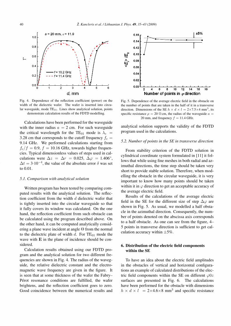
Fig. 5. Dependence of the average electric field in the obstacle onthe number of points that are taken in the half of it in a transversedirection. Dimensions of the SE h × d × l = 2×7.5×4 mm3, itsspecific resistance ρ = 20 Ω cm, the radius of the waveguide a =
20 mm, and frequency f = 11.4 GHz.
analytical solution supports the validity of the FDTDprogram used in the calculations.
5.2. Number of points in the SE in transverse direction
From stability criterion of the FDTD solution incylindrical coordinate system formulated in [11] it fol-lows that while using fine meshes in both radial and az-imuthal directions, the time step should be taken veryshort to provide stable solution. Therefore, when mod-elling the obstacle in the circular waveguide, it is veryimportant to know how many points should be takenwithin it in ϕ direction to get an acceptable accuracy ofthe average electric field.
Results of the calculations of the average electricfield in the SE for the different size of step ∆ϕ areshown in Fig. 5. As usual, we modelled a half obsta-cle in the azimuthal direction. Consequently, the num-ber of points denoted on the abscissa axis correspondsto a half obstacle. As one can see from the figure, 4–5 points in transverse direction is sufficient to get cal-culation accuracy within ±5%.
6. Distribution of the electric field componentswithin the SE
To have an idea about the electric field amplitudesin the obstacles of vertical and horizontal configura-tions an example of calculated distributions of the elec-tric field components within the SE on different ϕ0zsurfaces are presented in Fig. 6. The calculationshave been performed for the obstacle with dimensionsh × d × l = 2×4.6×8 mm3 and specific resistance

Ž. Kancleris et al. / Lithuanian J. Phys. 49, 35–43 (2009) 41
Fig. 6. Calculated distribution of the electric field components on a ϕ0z surface for the semiconductor obstacle of ε = 11.9 placed on thewall of the circular waveguide: (a), (b), and (c) within an obstacle in vertical configuration, (e), (f), and (g) in horizontal configuration, (d)and (h) in all modelled structure. Top distribution is on the surface where the amplitude Eϕ is maximal in the regular TE01 wave, bottomdistribution is on the surface that corresponds to the midpoint of the sample in r direction. Dimensions of the SE h×d× l = 2×4.6×8 mm3,ρ = 20 Ω cm; the obstacle is modelled by 4×5×16 cells; frequency 10.2 GHz; waveguide radius 20 mm; ∆r = ∆z = 0.025, ∆ϕ = 1.4,
∆t = 3.05·10−4.

42 Ž. Kancleris et al. / Lithuanian J. Phys. 49, 35–43 (2009)
of 20 Ω cm. The SE was modelled by 4×5×16 cells,the frequency was 10.2 GHz, and the waveguide ra-dius was 20 mm. Since the distribution of electricfield components is symmetric, only a half of the SEis shown in the figures.
Although the electric field in the regular TE01 wavehas the only component Eϕ, in the obstacle Er and Ez
are also excited. As one can see from Fig. 6, Er andEz are zero in the symmetry plane (ϕ = 0). Since theobstacle is symmetric with respect to the x0z plane,the waves propagating in the left and right side of thewaveguide should also be symmetric. Therefore, theexcited additional components, namely, Er, Ez , andHϕ should be antisymmetric:
Er(t, r, ϕ, z) = −Er(t, r, 360−ϕ, z) , (16)
and consequently in the symmetry plane they should bezero.
Although the electric field in the regular TE01 wavehas the only component Eϕ, the metal contact on thetop of the SE in the vertical configuration effectivelyprevents the penetration of Eϕ into the bulk of the ob-stacle. The main electrical component in the obstaclefor this case is Er. As already mentioned, this com-ponent is antisymmetric therefore it decreases to zeroin the symmetry plane of the obstacle. As one can seefrom Fig. 6(a–c), the difference between electric fieldamplitudes on different surfaces is not so large. Closerto the upper contact the electric field amplitude slightlyincreases.
Considering electric field amplitude in the horizon-tal configuration (Fig. 6(e–g)) one can see that Eϕ com-ponent, the only component in the regular TE01 wave,is the largest in the obstacle. Er goes to zero at ϕ =0 due to symmetry (16) and approaches zero near theside wall of the obstacle due to a boundary conditionfor the tangential electric field near the metal surface.The same behaviour is characteristic of the componentEz .
One can notice that the averaged electric field in theobstacle mainly consists of a single component, Er invertical and Eϕ in horizontal configuration, and thesame order of magnitude of the averaged electric fieldis characteristic of the both configurations. The aver-age amplitudes of the other two components are muchless than the dominant one.
However, as one can see from the distributions ofthe components in all modelled space presented in (d)and (h) subplots of the figure, horizontal configurationof the sensor introduces a smaller perturbation of theelectric field in the plane of maximal Eϕ amplitude
and smaller amplitude of reflections. For this partic-ular case VSWR introduced by the obstacle was 1.09and 1.06 for the vertical and horizontal configuration,respectively. Such effect can be attributed to the orien-tation of the metal contacts with respect to the electricfield of the incident wave. In general, the reflectionfrom the obstacle is sufficiently small in both cases andthe both configurations can be used as prototypes of theRS in the circular waveguide.
7. Conclusions
The peculiarities of interaction of the semiconduc-tor obstacle placed on a wall of a circular waveguidewith the mode TE01 have been investigated. Two dif-ferent structures have been considered, with the con-tacts on top and bottom planes (vertical configuration)and with the contacts on sidewalls (horizontal config-uration). A program based on the FDTD method waswritten, tested, and used for the calculation of the elec-tromagnetic field components in cylindrical waveguide,reflection coefficient from the semiconductor obstacle,and the average electric field in it employing cylindri-cal coordinate system. The distribution of electric fieldcomponents within the semiconductor obstacle placedon a wall of a circular waveguide and in all modelledstructure has been calculated. The averaged electricfield in the obstacle mainly consists of a single com-ponent, Er in vertical and Eϕ in horizontal configura-tion, and the same order of magnitude of the averagedelectric field is characteristic of the both configurations.The average amplitudes of the other two componentsare much less than the dominant one. The reflectionfrom the obstacle is sufficiently small in both cases andthe both configurations can be used as prototypes of theRS in the circular waveguide. The model and programproposed here could be used for the calculation of theoptimal sensors parameters.
Acknowledgements
The work has been supported by the Air Force Of-fice of Scientific Research, Air Force Material Com-mand, USAF, under grant number FA8655-07-1-3028.Authors would like to acknowledge the partial supportof this work by Directorate-General for Justice, Free-dom and Security of the European Commission underthe project “Assessment and mitigation of risk for dis-abling control centre of large power networks by inten-tional radiofrequency interference”.

Ž. Kancleris et al. / Lithuanian J. Phys. 49, 35–43 (2009) 43
References
[1] R. Chatterjee, Elements of Microwave Engineering(John Wiley & Sons, New York, Chichester, Brisbane,Toronto, 1986).
[2] T.A. Spencer, C.E. Davis, K.J. Hendricks, F.J. Agee,and R.M. Gilgenbach, Results from gyrotron back-ward wave oscillator experiments utilizing a high-current high-voltage annular electron beam, IEEETrans. Plasma Sci. 24(3), 630–635 (1996).
[3] S.G. Tantawi, A novel circular TE01-mode bend forultra-high-power applications, J. Electromag, WavesAppl. 18(12), 1679–1687 (2004).
[4] S.G. Tantawi, R.D. Ruth, A.E. Vlieks, and M. Zolo-torev, Active high–power RF pulse compression usingoptically switched resonant delay lines, IEEE Trans.Microwave Theory Tech. 45(8), 1486–1492 (1997).
[5] J. Neilson, L. Ives, and S.G. Tantawi, Design and testof a 100 MW-band TE01 window, in: Proceedingsof the 2003 Particle Accelerator Conference, (2003)p. 1125–1126.
[6] J. Neilson and L. Ives, Development of a multi–megawatt circulator for X-band, in: Proceedings of the2003 Particle Accelerator Conference, (2003) p. 1127.
[7] M. Dagys, Ž. Kancleris, R. Simniškis, E. Schamiloglu,and F.J. Agee, Resistive sensor: Device for high-powermicrowave pulse measurement, IEEE Antenn. Propag.Mag. 43(5), 64–79 (2001).
[8] S.I. Baskakov, Basics of Electrodynamics (Soviet Ra-dio, Moscow, 1973) [in Russian].
[9] Kane S. Yee, Numerical solution of initial bound-ary value problems involving Maxwell’s equation in
isotropic media, IEEE Trans. Antenn. Propag. 14(3),302–307, (1966).
[10] A. Taflove, Computational Electrodynamics: TheFinite-Difference Time-Domain Method (ArtechHouse, Norwood, MA, 1995).
[11] Q. Chen and V. Fusco, Three dimensional cylindri-cal coordinate finite difference time domain analysisof curved slotline, in: 2nd International Conferenceon Computations in Electromagnetism, Nottingham,U.K., May 13–15, 1994, pp. 323–326.
[12] Y. Chen, R. Mittra, and P. Harms, Finite-differencetime-domain algorithm for solving Maxwell’s equationin rotationally symmetric geometries, IEEE Trans. Mi-crowave Theory Tech. 44(6), 832–839 (1996).
[13] N. Dib, T Weller, M Scardeletti, and M. Imparato,Analysis of cylindrical transmission lines with thefinite-difference time-domain method, IEEE Trans.Microwave Theory Tech. 47(4), 509–512 (1999).
[14] F. Liu and S. Crozier, An FDTD model for calcula-tion of gradient-induced eddy currents in MRI sys-tem, IEEE Trans. Appl. Supercond. 14(9), 1983–1989(2004).
[15] A. Trakic, H. Wang, F. Liu, H.S. López, and S. Crozier,Analysis of transient eddy currents in MRI using acylindrical FDTD method, IEEE Trans. Appl. Super-cond. 16(3), 1924–1936 (2006).
[16] Ž. Kancleris, Handling of singularity in finite-difference time-domain procedure for solvingMaxwell’s equations in cylindrical coordinate system,IEEE Trans. Antenn. Propag. 56(2), 610–613 (2008).
PUSLAIDININKINES PLOKŠTELES SAVEIKA SU TE01 MODA APVALIAJAME BANGOLAIDYJE
Ž. Kancleris, G. Šlekas, V. Tamošiunas, R. Simniškis, P. Ragulis, M. Tamošiuniene
Puslaidininkiu fizikos institutas, Vilnius, Lietuva
SantraukaApžvelgti TE01 (H01) modos, sklindancios apvaliuoju bango-
laidžiu, privalumai bei panaudojimas kuriant mikrobangu prietai-sus. Išnagrineta galimybe sukurti rezistorini jutikli, skirta dide-les galios mikrobangu impulsams matuoti, panaudojant puslaidi-ninkine kliuti, esancia ant apvaliojo bangolaidžio sieneles. Pa-siulytos dvi jutiklio jautraus elemento realizacijos: vertikalioji,kai kontaktai yra sukurti ant viršutinio ir apatinio puslaidininkinesplokšteles paviršiu, ir horizontalioji, kai metaliniai kontaktai sufor-muoti ant šoniniu jutiklio plokštumu. Aptartos galimos praktinesjutikliu realizacijos, panaudojant plokšcius jutiklius kaip jautriuo-sius elementus. Pasirinktas puslaidininkines kliuties modelis ir pa-
teiktas Maksvelo lygciu cilindrineje koordinaciu sistemoje spren-dimo metodas. Elektromagnetinio lauko sandu skaiciavimui buvonaudojamas baigtiniu skirtumu laiko skaleje metodas. AprašytaC++ programa, sukurta vidutiniam elektriniam laukui puslaidinin-kineje kliutyje ir atspindžio koeficientui nuo jo skaiciuoti. Sukurtosprogramos patikrintos lyginant skaiciavimo rezultatus su analiziniusprendiniu. Apskaiciuotas elektrinio lauko pasiskirstymas vertika-lios ir horizontalios konfiguracijos puslaidininkineje kliutyje, esan-cioje ant apvaliojo bangolaidžio vidines sieneles, ir visame mode-liuotame darinyje. Pasirode, kad vertikalios konfiguracijos jutiklioviduje dominuoja Er elektrinio lauko sandas, kai tuo tarpu hori-zontalios konfiguracijos jutiklyje didžiausias sandas yra Eϕ.