semiconductor process technology, equipment, materials & manufacturing · semiconductor process...
TRANSCRIPT
Semiconductor Process Technology, Equipment, Materials & Manufacturing
• Jo De Boeck
• Arco Krijgsman

Semiconductor Process Technology, Equipment, Materials & Manufacturing Overall SRA Process
2
Dec ‘17 Jan ‘18Aug ‘17 Sep ‘17Apr ‘17 May ‘17 Jun ‘17 Jul ‘17 Nov ‘17Oct ‘17
Outline & teams definition
First draft
Second draft
for comments
by community
Final version
Team, half page & « Game Changers » description
V1 – Majorchallengesidentified
V3 – For review by assoc.mgtbodies
V2 – For review by assoc. expert councils.Topic & Major Challenges
V5 – Finaldraft for review by assoc.mgtbodies
Finalversion
May 4Kick-off
Dec 5-6EFECSWorkshopsDec 7th Core team& chaptersleaders
April 19Core team1st meeting
June 9Core team& chapterleaders
July 4Core team& chapterleaders
Sep 7Core team& chapterleaders
Oct 12Core team& chapterleaders
Beg Nov.(no mtg)
Dec 18(no mtgExcept if needed)
End Jan(no mtg)
July 18Coreteam
Aug 25Coreteam
Sep 29Coreteam
Oct 18Coreteam
V4 – Publiclyavailablefor comments+ PreliminaryinputTo ECSEL MASP
Nov 20Core team+ comm.
Over 250 expertsacross core team + 10 chapter teams

Semiconductor Process Technology, Equipment, Materials & ManufacturingOverall SRA structure
3
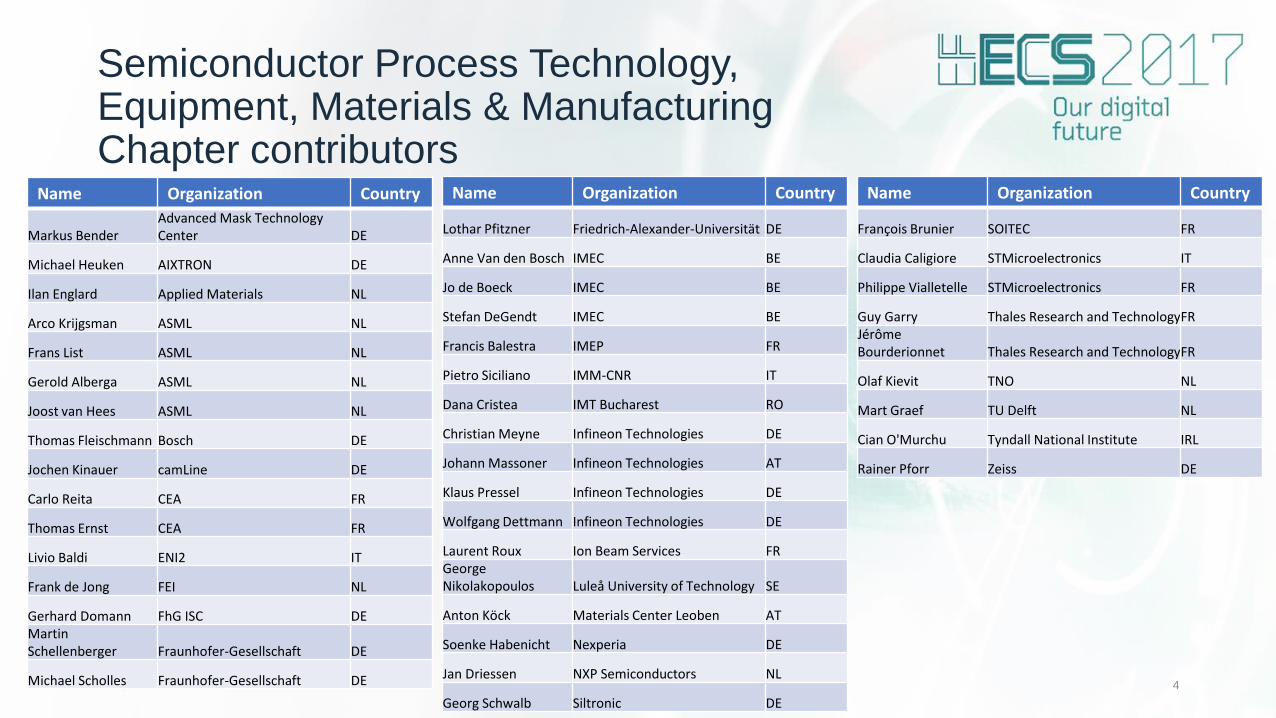
Semiconductor Process Technology, Equipment, Materials & ManufacturingChapter contributors
Name Organization Country
Markus BenderAdvanced Mask Technology Center DE
Michael Heuken AIXTRON DE
Ilan Englard Applied Materials NL
Arco Krijgsman ASML NL
Frans List ASML NL
Gerold Alberga ASML NL
Joost van Hees ASML NL
Thomas Fleischmann Bosch DE
Jochen Kinauer camLine DE
Carlo Reita CEA FR
Thomas Ernst CEA FR
Livio Baldi ENI2 IT
Frank de Jong FEI NL
Gerhard Domann FhG ISC DEMartin Schellenberger Fraunhofer-Gesellschaft DE
Michael Scholles Fraunhofer-Gesellschaft DE 4
Name Organization Country
Lothar Pfitzner Friedrich-Alexander-Universität DE
Anne Van den Bosch IMEC BE
Jo de Boeck IMEC BE
Stefan DeGendt IMEC BE
Francis Balestra IMEP FR
Pietro Siciliano IMM-CNR IT
Dana Cristea IMT Bucharest RO
Christian Meyne Infineon Technologies DE
Johann Massoner Infineon Technologies AT
Klaus Pressel Infineon Technologies DE
Wolfgang Dettmann Infineon Technologies DE
Laurent Roux Ion Beam Services FRGeorge Nikolakopoulos Luleå University of Technology SE
Anton Köck Materials Center Leoben AT
Soenke Habenicht Nexperia DE
Jan Driessen NXP Semiconductors NL
Georg Schwalb Siltronic DE
Name Organization Country
François Brunier SOITEC FR
Claudia Caligiore STMicroelectronics IT
Philippe Vialletelle STMicroelectronics FR
Guy Garry Thales Research and TechnologyFRJérôme Bourderionnet Thales Research and TechnologyFR
Olaf Kievit TNO NL
Mart Graef TU Delft NL
Cian O'Murchu Tyndall National Institute IRL
Rainer Pforr Zeiss DE

Semiconductor Process Technology, Equipment, Materials & Manufacturing Core team structure
Overall editing:
• Secure overall integrity & consistency of the document
Role Team members
Coordinators Jo de Boeck / Arco Krijgsman
Overall editing Livio Baldi
Topic Lead Performance scaling
System in Package
System on Chip SemiconEquipment &
Manufacturing
Francis BalestraKlaus Pressel /
Thomas FleischmannRainer Pforr / Ilan Englard
Topic leads:
• Represent the contributors on this topic in the core team
• Make sure the contributions from all contributors are taken into the ECS agenda
• Make sure the roadmap timeline matches

Semiconductor Process Technology, Equipment, Materials & ManufacturingWorkshop session September 26th 2017
1. Developing advanced, logic and
memory technology for nanoscale
integration and application-driven
performance
2. More than Moore and
Heterogeneous System-on-Chip (SoC)
Integration;
3. Advanced smart System-in-
Package (SiP) applications
4. Maintaining world leadership in
Semiconductor Equipment, Materials
and Manufacturing solutions.
IMEP ASML IMEC
Francis Balestra Gerold Alberga Stefan DeGendt
FR NL BE
Applied Materials TU Delft
Ilan Englard Mart Graef
NL NL
Zeiss TNO ASML
Rainer Pforr Olaf Kievit Arco Krijgsman
DE NL NL
Infineon
Technologies
CEA
Christian Meyne Thomas Ernst
DE FR
Tyndall National
Institute
FhG ISC ASML
Cian O'Murchu Gerhard Domann Frans List
IRL DE NL
Bosch Infineon
Technologies
Thomas
Fleischmann
Klaus Pressel
DE DE
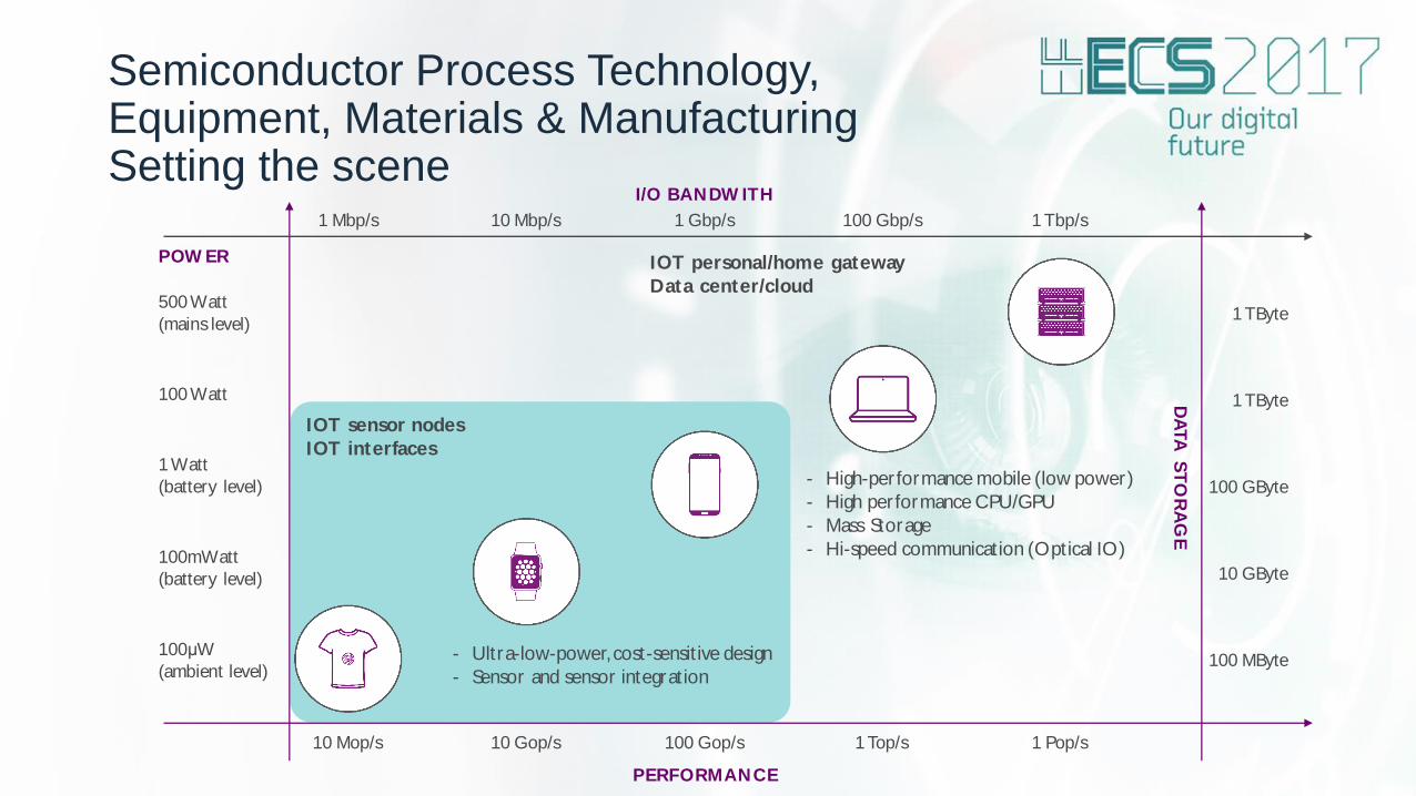
500 Watt
(mains level)
POW ER
100 Watt
1 Watt
(battery level)
100mWatt
(battery level)
100µW
(ambient level)
1 Mbp/s 10 Mbp/s 1 Gbp/s 100 Gbp/s 1 Tbp/s
I/O BANDW ITH
10 Mop/s 10 Gop/s 100 Gop/s 1 Top/s 1 Pop/s
PERFORMANCE
100 MByte
10 GByte
100 GByte
1 TByte
1 TByte
- High-performance mobile (low power)
- High performance CPU/GPU
- Mass Storage
- Hi-speed communication (Optical IO)
IOT personal/home gateway
Data center/cloud
IOT sensor nodes
IOT interfaces
- Ultra-low-power, cost-sensit ive design
- Sensor and sensor integration
DA
TA
ST
OR
AG
E
Semiconductor Process Technology, Equipment, Materials & Manufacturing Setting the scene

Semiconductor Process Technology, Equipment, Materials & ManufacturingMajor Challenges
1. Developing advanced, logic and memory technology for nanoscale integration and application-driven performance;
2. More than Moore and Heterogeneous System-on-Chip (SoC) Integration;
3. Advanced smart System-in-Package (SiP) applications;
4. Maintaining world leadership in Semiconductor Equipment, Materials and Manufacturing solutions.

Semiconductor Process Technology, Equipment, Materials & ManufacturingMajor Challenge 1
Developing advanced logic and memory technology for nanoscale integration and application-driven performance
2029 2030
CMOS technology platform generations
22 nm FDX implementation (Strained PFET, in-situ doped RSD(Gen1), Gate first)
FINFET implementation >N7 / 12nm FDx (Strained CMOS), in situ doped RSD(Gen2), dual STI)
<N7 horizontal Gate-All-Around NW/ 10 nm FDX (Gate Last, SAC)
<N5 Vertical GAA
Beyond CMOS & new compute paradigm options down-select and implement Spin transistors, Steep sub-Vt slope (FeFET, TFET, NEMS), alternative materials: TMD's, others
Integrated (embedded NVM) memory systems incl. new storagr architectures for smart systems, IoT and new compute paradigms
STT-MRAM / ReRAM / PCM / other
Wafer based process technologies for 3D integration (cfr also Challenge 3) including (monolithic) 3D-IC
implementation pilots
20252018 2019 2020 2026 20272021 2022 2023
Maj
or
Ch
alle
nge
1:
'Dev
elo
pin
g ad
van
ced
logi
c
and
mem
ory
tec
hn
olo
gy f
or
nan
osc
ale
inte
grat
ion
an
d
app
licat
ion
-dri
ven
per
form
ance
'
20282024
As already evidenced in the latest versions of IRDS (International Roadmap for Devices and Systems), device density and switching speed are no more the single performance indicator for logic devices. Low power (stand-by and operational) and high operating temperature are of greater importance for European critical applications like Health, IoT and Automotive/Industrial.

Semiconductor Process Technology, Equipment, Materials & ManufacturingMajor Challenge 2
More than Moore and Heterogeneous System-on-Chip (SoC) Integration
2029 2030
Technology platform for integrated application defined sensors, including packaging
implementation pilots
Process technology platforms for new RF and mm-wave integrated device options, incl. radar (SiGe/BiCMOS, FDX, CMOS), photonics options, as well as packaging
implementation pilots
Process technology platforms for biomedical devices for minimally invasive healthcare
implementation pilots
Process technology platforms for power electronics
e.g. higher P density & freq., wide-gap, new CMOS/IGBT processes, integrated logic, uni-& bipolar, higher V-classes, lateral to vertical arch as well as packaging
Process technology exploration for functional integration of novel materials (e.g. Graphene, TMD's, FerroElectric, Magnetic, e.a. ) implemented in existing pilot line
implementation pilots
20252018 2019 2020 2026 20272021 2022 2023
Maj
or
Ch
alle
nge
2:
'Mo
re t
han
Mo
ore
an
d
Het
ero
gen
eou
s Sy
stem
-on
-Ch
ip
(So
C)
Inte
grat
ion
'
20282024
The realization of smart electronic components and systems for European critical applications requires complementing logic and memories with additional features, which are non-scalable with Moore’s Law, to handle the functions of sensing, actuation, communication, data protection and power management. These heterogeneous functionalities can be integrated on the same System-on-Chip, such as for embedded memories, and for analogue and Smart Power, or realized as discrete components for SiP integration. Advanced technologies, processes and materials need to be developed for innovative More-than-Moore solutions. They enable innovative emerging applications, while leveraging synergies with processing and manufacturing technologies of More-Moore devices.

Semiconductor Process Technology, Equipment, Materials & ManufacturingMajor Challenge 3
Advanced smart System-in-Package (SiP) applications
2029 2030
Process technology for multi-chip embedding (molded, PCB, flexible substrate, silicon)
Multi-die embedding (molded, la implementation pilots next gen systems / new applications
… in flexible substrates implementation pilots next gen systems / new applications
Process technology for heterogeneous and (2.5 & 3D) SiP integration
wafer level, interposer (Si), various technologies, e.g. GaN, SiC, Logic & power embedding, intelligent power modules, optical interc.
SiP Technologies (thin wafer/die handling, dicing, stacking) next gen systems / new applications
Si interposer (TSV), passive, RF-SiP (glass) and sensor integration next gen systems / new applications
Continuous improvement of (i) Materials aspects, (ii) Thermal management
(iii) high temperature package (iv) Characterization & modleing, (v) Reliability & failure analysis & test
continuous improvements continuous improvements
iv) Characterization & modleing, (v) Reliability & failure analysis & test, but needs parallel ongoing basic reseach
20252018 2019 2020 2026 20272021 2022 2023
Maj
or
Ch
alle
nge
3:
'Het
ero
gen
eou
s Sy
stem
-in
-
Pac
kage
(Si
P)
inte
grat
ion
'
20282024
Advanced SiP technologies are required to deliver the functionality in meeting the demanding specifications and boundary conditions of major electronic component applications. The integration of more functionality in smaller volume requires new assembly and packaging materials, compatible chip/package interfaces, as well as heterogeneous integration of chips with different functionalities like MEMS/sensors, power chips, processors, or memory. Special focus must be on electrical capabilities and temperature constraints keeping robustness and reliability for the applications.

Semiconductor Process Technology, Equipment, Materials & ManufacturingMajor Challenge 4
Maintaining world leadership in Semiconductor Equipment, Materials and Manufacturing solutions
Supply the European ECS manufacturing companies with ‘best-in-class’ equipment and materials, and flexible, agile and competitive semiconductor manufacturing solutions in the domains More Moore (MM), More than Moore (MtM) and System in Package, and by this the European application sector to compete on the world markets with top quality products.

Semiconductor Process Technology, Equipment, Materials & ManufacturingMajor Challenge 4
Maintaining world leadership in Semiconductor Equipment, Materials and Manufacturing solutions
Defend and extend Europe’s world leadership positions in Semiconductor Equipment, Materials and Manufacturing solutions. Supply the European ECS manufacturing companies with ‘best-in-class’ equipment and materials, and flexible, agile and competitive semiconductor manufacturing solutions in the domains More Moore (MM), More than Moore (MtM) and System in Package, and by this the European application sector to compete on the world markets with top quality products.
2029 2030
More Moore: Equipment & Materials for sub-10nm semiconductor devices & systems manufacturing
Equipment & materials for 7nm node °
Equipment & materials for 5nm node °
Equipment & materials for 3nm node °
Equipment & materials for sub 3nm node °
Metrology & inspection equipment for 7nm node
Metrology & inspection for 5nm node
Metrology & inspection equipment for 3nm node
Metrology & inspection equipment for sub 3nm node
Equipment , Materials, Metrology & inspection for Beyond CMOS & new compute paradigm options
More than Moore and Heterogeneous SoC & SiP integration equipment and materials
Equipment enabling Heterogeneous Integration
Innovative materials enabling Heterogeneous Integration (on chip & package level)
Specific equipments and materials enabling innovative MTM devices and heterogeneous integration
E&M for further miniaturization and higher functional density for MTM
Upgrade MTM technologies to 300mm wafers and heterogeneous SiP integration
Manufacturing technologies
Upgrade automation, APC and integration of new sensors and hybrid solutions
Control of variability in manufacturing
Advanced diagnostic and decision support systems (supervision, scheduling, agility)
Knowledge management (inter fab flows, fast diagnosis)
FICS migration toward distributed architecture BYOD / Apps
20252018 2019 2020 2026 20272021 2022 2023
Maj
or
Ch
alle
nge
4:
'Mai
nta
inin
g w
orl
d le
ader
ship
wit
h
Sem
ico
nd
uct
or
Equ
ipm
ent,
Mat
eria
ls
and
Man
ufa
ctu
rin
g so
luti
on
s.'
20282024

R&I funding instrument landscape
NATIONAL
Develop & Maintain
Critical Mass
National contract
EUREKA
Trans-National
Programmes
National Priorities
National contract
H2020
Innovation & Infrastructure
European Priorities
EC contract
ECSEL-JU
ECS Programmes
National & European
Priorities
EC contract & National
contract
NATIONAL CROSS BORDER COOPERATION
NATIONAL FUNDINGEUROPEAN FUNDING

15
ECS-related R&I funding programme informationAvailable in the Exhibition Hall ECSEL 2018 RIA and IA calls:
• Calls open: 21/02/2018• Project Outline deadline:
26/04/2018• Full Project Proposal deadline:
20/09/2018
Based on ECS SRA
Open, deadline for PO February 13th, 2017
Open, closing dateFebruary 15th 2018
PO deadline March 12th 2018
Call opens Dec 11th 2017PO deadline March 9th 2018
Call closure April 23rd, 2018
Call open, cut-off date March 1st, 2018
PO deadline March 12th 2018

Semiconductor Process Technology, Equipment, Materials & ManufacturingThe floor is yours!
• Questions?
• Feedback?
• Inputs?
16

Semiconductor Process Technology, Equipment, Materials & Manufacturing
Pitches

Semiconductor Process Technology, Equipment, Materials & Manufacturing
18
Idea Name Presenter Organization Poster/Pitch
Next GaN Michael Salter Acreo Swedish ICT AB Pitch
LUniHar Christian Hedayat Fraunhofer ENAS-PB Pitch
Nano-R, MSP-X & MSP-R Anton Koeck Materials Center Leoben Forschung GmbH (MCL)
Pitch
INTELLIGENT Martin Landgraf Fraunhofer IPMS Pitch
LAMP Anneliese Poenninger EV Group Poster
PLIANTLY Jacques Perocheau LCP'S Engineering Poster
Pitched ideas

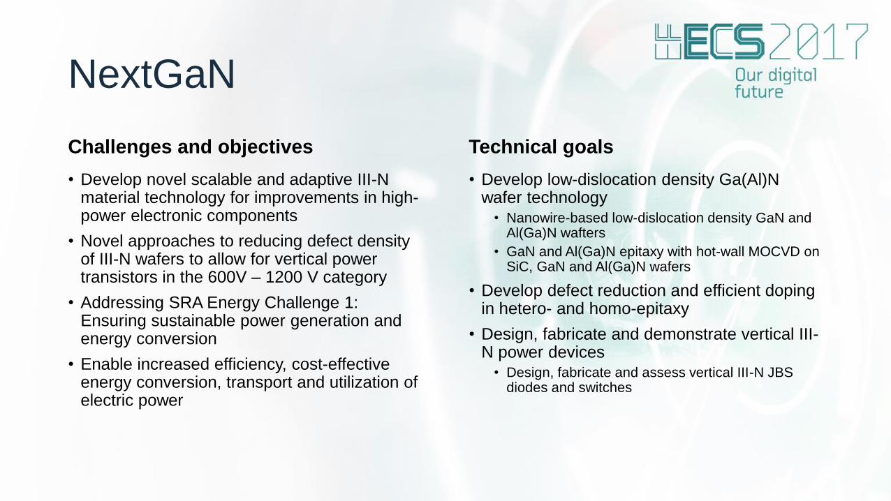
NextGaN
Next generation, high power, high efficiency III-N components through innovations in material and process technologies
Michael Salter – [email protected]
NextGaN
Challenges and objectives
• Develop novel scalable and adaptive III-N material technology for improvements in high-power electronic components
• Novel approaches to reducing defect density of III-N wafers to allow for vertical power transistors in the 600V – 1200 V category
• Addressing SRA Energy Challenge 1: Ensuring sustainable power generation and energy conversion
• Enable increased efficiency, cost-effective energy conversion, transport and utilization of electric power
Technical goals
• Develop low-dislocation density Ga(Al)N wafer technology
• Nanowire-based low-dislocation density GaN and Al(Ga)N wafters
• GaN and Al(Ga)N epitaxy with hot-wall MOCVD on SiC, GaN and Al(Ga)N wafers
• Develop defect reduction and efficient doping in hetero- and homo-epitaxy
• Design, fabricate and demonstrate vertical III-N power devices
• Design, fabricate and assess vertical III-N JBS diodes and switches

NextGaN
Current Partners
• ON Semiconductor, ABB (LE)
• SweGaN, Hexagem (SME)
• Linköping, Lund, Chalmers (University)
• RISE (RTO)
Contact
• [email protected], +46 703 55 5838
Desired Partners
• Power electronic device manufacturing companies
• Power electronic subsystem companies
• Power equipment and Energy OEMs
• Passive component manufactures
• University and RTOs
• Other national power consortiums/projects


Nano-R
Fabrication and Reliability of Nanodevices based on 0D, 1D, & 2D Nanomaterials
Anton Köck – [email protected]

Nano-R
Challenges and objectives
• Novel nanomaterials enable entirely new applications (Graphene, MoS2, nanowires, quantum dots…)
• How to fabricate and integrate such nanomaterials on CMOS based devices ?
• How to fabricate new “Si-less” nanodevices ?
• How to analyse the nanodevices ?
Technical goals
• Fabrication and integration technologies
• Lot of reliability issues !!!
• E.g. electrical contacts
• Novel analysis tools and technologies from macro to nano along production chain

Nano-R
Partners
• Materials Center Leoben (MCL)
• University of Oxford
• KTH Stockholm
• ETH Zürich
• EVGroup
• Etc.
• Which call….?
Economical impact (optional)
• Entirely new sensor devices
• Entirely new light emitting devices
• Energy storage & energy harvesting
• Ultra low power devices for IoT and wearables
Contact
• Anton Köck, +43(0)3842-45922-505
Expected Duration / budget (optional)
• 48 months, XXXX k€

MSP-R
Multi Sensor Platform – Reliability of 3D-integrated Multi Sensor Systems
Anton Köck – [email protected]

MSP-R
Challenges and objectives
• The project is based on the MSP-project
• 3D-integration of 57 nano-based sensor devices !
• Focus on specific combinations of sensor devices
Technical goals
• 3D-integration technologies
• 3D-integration in more (than 2) layers !
• Overmolding of 3D-integrated system
• Reliability issues !!! Analysis tools and technologies from macro to nano along production chain !

Project idea name
Partners
• Materials Center Leoben
• Holst Center imec Netherlands
• Ams AG
• Infineon
• Besi
• Boschman
• Etc.
• ECSEL-project
Economical impact (optional)
• Reliable multi-sensor system capable for IoT-applications
• Multi-sensor systems for wearables, smart phones, wristband devices
• Consumer Electronics
• Smart Home, Smart Building, Smart Cities,…
Contact
• Anton Köck, +43(0)3842-45922-505
Expected Duration / budget (optional)
• 36 months, 10000 k€

MSP-Xtreme
Multi Sensor Platform - Extreme Miniaturisation & Integration for IoT Applications
Anton Köck – [email protected]

MSP-Xtreme
Challenges and objectives
• The project is based on the MSP-project
• 57 integrated sensor devices !
• 3D-integration of nanotechnology based sensors for environmental monitoring
• Development of energy autonomous system
Technical goals
• Ultra-low power sensing devices
• Energy harvesting (Perovskite or Quantum Dots) & Energy storage (Super-Cap)
• Wireless transmission
• Reliability issues !!! Advanced analysis tools and technologies from macro to nano along production chain !

Project idea name
Partners
• Materials Center Leoben (MCL)
• Holst Center imec Netherlands
• University Barcelona
• University of Oxford
• TNO (Solliance Solar Research)
• Etc.
• ICT-Call ICT-07-2018 Electronic Smart System
Economical impact (optional)
• Energy autonomous multi-sensor system capable for IoT-applications
• Consumer electronics, wearables
• Smart Home, Smart Building, Smart Cities
Contact
• Anton Köck, +43(0)3842-45922-505
Expected Duration / budget (optional)
• 36 months, 6000 k€

INTELLIGENT
New BEOL based Non-Volatile Memory for low-power applications
Martin Landgraf – Fraunhofer IPMS, Dresden, Germany
- Funding Project Management -

Standard CMOS baselinefrom Waferfab
INTELLIGENTIntroduction of new functional layers into general electronics for non-volatile memory technologies
PMOSNMOS
M1
M2
M3
M4
M5
M6
Standard CMOS
M7
M8
M9
New BEOL based Non-Volatile Memory
Introduction of HfO based ferroelectric layers into the BEoL on FeFET basis (1T-1C integration)
Advantages:
• Low power (< 4V program/erase)
• Small size (bitcell footprint)
• Low cost (few additional litho layers only)
• independent integration from FEoL(use standard CMOS baseline)
Application fields:
• low power embedded memory solutions (e.g. IoT, metering, data logging, self-powered systems)

INTELLIGENTIntroduction of new functional layers into general electronics for non-volatile memory technologies
Search for following partners:
• System integrators and end user with need for embedded NVM in low-power application
• Partner for array design & simulations
Contact
[email protected] (funding project management)
[email protected] (group manager NVM)
Expected Duration / Budget
36 months / tbd
Standard FeFET
FE material in Front-End
FE material separated in
Back-End
Project Goal
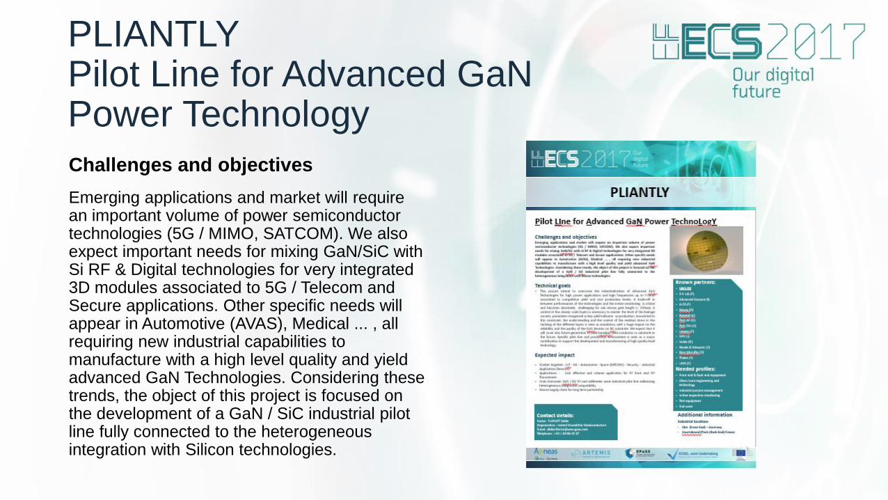
PLIANTLYPilot Line for Advanced GaNPower Technology
Challenges and objectives
Emerging applications and market will require an important volume of power semiconductor technologies (5G / MIMO, SATCOM). We also expect important needs for mixing GaN/SiC with Si RF & Digital technologies for very integrated 3D modules associated to 5G / Telecom and Secure applications. Other specific needs will appear in Automotive (AVAS), Medical ... , all requiring new industrial capabilities to manufacture with a high level quality and yield advanced GaN Technologies. Considering these trends, the object of this project is focused on the development of a GaN / SiC industrial pilot line fully connected to the heterogeneous integration with Silicon technologies.

LAMPLarge Surface Nano Imprint Lithography

Semiconductor Process Technology, Equipment, Materials & Manufacturing
Semiconductor Process Technology, Equipment, Materials & ManufacturingContact Information
Jo DeBoeck
Imec
42
Arco Krijgsman
ASML