semiconductor spintronics - nanotechnology, ieee ...€¦ · semiconductor spintronics hiro akinaga...
TRANSCRIPT
IEEE TRANSACTIONS ON NANOTECHNOLOGY, VOL. 1, NO. 1, MARCH 2002 19
Semiconductor SpintronicsHiro Akinaga and Hideo Ohno, Member, IEEE
Abstract—We review recent progress made in the field ofsemiconductor spintronics, a branch of semiconductor electronicswhere both charge and spin degrees of freedom play an importantrole in realizing unique functionalities. We first describe the newspin-dependent phenomena found in semiconductors includingcarrier-induced ferromagnetism in III–V compounds, followed byan account of our current understanding of such spin-dependentphenomena. Then we summarize the challenges the semicon-ductor spintronics has to meet in order for it to be a success as“electronics.”
Index Terms—Ferromagnetic semiconductors, magnetooptic(MO) devices, magnetoresistive devices, quantum information,spin coherence.
I. INTRODUCTION
T HE SUCCESS of semiconductor electronics has been builton the charge degree of freedom of electrons in semicon-
ductors. The spin degree of freedom, used in magnetic massstorage, has long been neglected in semiconductors because ofthe almost degenerate energies of the two spin states of electronsin semiconductors. However, because of the advances in semi-conductor science and technology, the control and manipulationof the spin degree of freedom in semiconductors is becomingincreasingly possible [1]–[3]. In addition, semiconductor tech-nology has continuously reduced its working dimension to meetthe demand for faster and denser integrated circuits. This leadsus to a nanoscale dimension, where exchange interaction (aspin-dependent interaction) among carriers can no longer beignored; like it or not, we will inevitably have to work with spindependent interactions in semiconductors in the near future.Progress in magnetic imaging technologies has also startedto reveal spin-dependent phenomena in nanoscale structures[4]. All these developments indicate that the time has come toexplore, understand and utilize the spin-dependent phenomenain semiconductors. This may lead us to further increase thefunctionalities of existing devices and circuits like using thecapability of mass storage and processing of information at the
Manuscript received February 2, 2002; revised February 26, 2002. Thework conducted at the National Institute of Advanced Industrial Scienceand Technology (AIST) was supported in part by the New Energy andIndustrial Technology Development Organization [Atom-Technology Projectand Synthetic Nano-Function Materials Project]. The work conducted atTohoku University was supported in part by the “Research for the Future”program of the Japan Society for the Promotion of Science under GrantJSPS-RFTF97P00202, and in part by Grant-in-Aids 1230500 and 09244103from the Ministry of Education, Culture, Sports, Science and Technology,Japan.
H. Akinaga is with the Nanotechnology Research Institute, National Insti-tute of Advanced Industrial Science and Technology (AIST), Ibaraki 305-8562,Japan.
H. Ohno is with the Laboratory for Electronic Intelligent Systems, ResearchInstitute of Electrical Communication, Tohoku University, Sendai 980-8577,Japan.
Publisher Item Identifier S 1536-125X(02)04583-0.
same time, and to realize quantum information technologiesusing spin as a qubit in solid state. This area of semiconductorelectronics is called semiconductor spintronics, where bothcharge and spin degrees of freedom play an important andindispensable role in realizing functionalities.
The latest semiconductor material technology offers a seriesof ferromagnetic semiconductors that are compatible with theexisting nonmagnetic semiconductors (contain no magneticelement like Mn). Such compatibility allows us to integrate, in asingle crystal structure, ferromagnetism with all the freedoms weare currently enjoying in semiconductors including heterostruc-tures. These ferromagnetic semiconductor heterostructure canthen be used to store information, amplify spin current, processinformation, and initialize and read-out spin quantum states.The combination of the advances in semiconductor materialscience,nanoscale physicsand device technology,and integratedcircuits, we should be able to polarize, inject, store, manipulate,and then detect spin information. To review current status, wesummarized the new freedoms in spin manipulations in SectionII. Section III describes our understanding of spin-dependentphenomena related to semiconductor spintronics. The prospectand challenges that we need to meet in the beginning of the21st century are outlined in Section IV.
II. SEMICONDUCTORSPINTRONICSOFFERS
A. Carrier-Induced Ferromagnetism
Recent developments in materials science and technology ofsemiconductors resulted in carrier-induced ferromagnetism insemiconductors that are currently used in transistors and lasers.Nonmagnetic semiconductors (i.e., containing no magneticions), such as GaAs, have been made magnetic by introducing asmall amount of magnetic ions (like Mn). The ferromagnetism(alignment of spins of magnetic ions) is brought about by thecarrier-mediated interaction among magnetic ions; withoutcarriers no ferromagnetism occurs. This carrier-induced fer-romagnetism in magnetic ion-doped semiconductors offers avariety of new controllability of semiconducting propertiesby magnetism and magnetism by semiconducting properties.When one changes carrier concentration by some externalmeans, which can be done in semiconductors but not in metals,magnetism changes. This electronic control of magnetism hasremained elusive but recently demonstrated in ferromagneticsemiconductors.
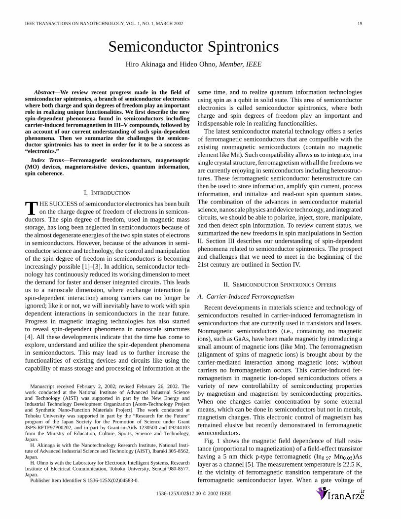
Fig. 1 shows the magnetic field dependence of Hall resis-tance (proportional to magnetization) of a field-effect transistorhaving a 5 nm thick p-type ferromagnetic (In Mn )Aslayer as a channel [5]. The measurement temperature is 22.5 K,in the vicinity of ferromagnetic transition temperature of theferromagnetic semiconductor layer. When a gate voltage of
1536-125X/02$17.00 © 2002 IEEE
20 IEEE TRANSACTIONS ON NANOTECHNOLOGY, VOL. 1, NO. 1, MARCH 2002
Fig. 1. Gate voltage dependence of Hall resistance in an (In,Mn)As FETstructure close to the ferromagnetic transition temperature. When a gatevoltage ofV = �125 V is applied, hysteresis is clearly observed. On theother hand, whenV = +125 V, the hysteresis disappears. This demonstratesthat the applied field is able to switch the device between ferromagnetic andparamagnetic states [5].
V is applied (electric field 1.6 10 V/cm), holesthat mediate ferromagnetic interaction are partially depletedresulting in decrease of the channel magnetization and inthe disappearance of hysteresis. Changing to 125 Vincreases the channel magnetization and hysteresis becomessquare. Virtually identical magnetization curve is restored uponreturning to V. This proof of concept demonstrationshows that one can switch ferromagnetic phase on and off byapplying external electric fields isothermally in a reversibleway. Although the electric-field control of ferromagnetism isdemonstrated at reduced temperatures, it opens up a range ofnew possibilities to control magneto-electronics devices.
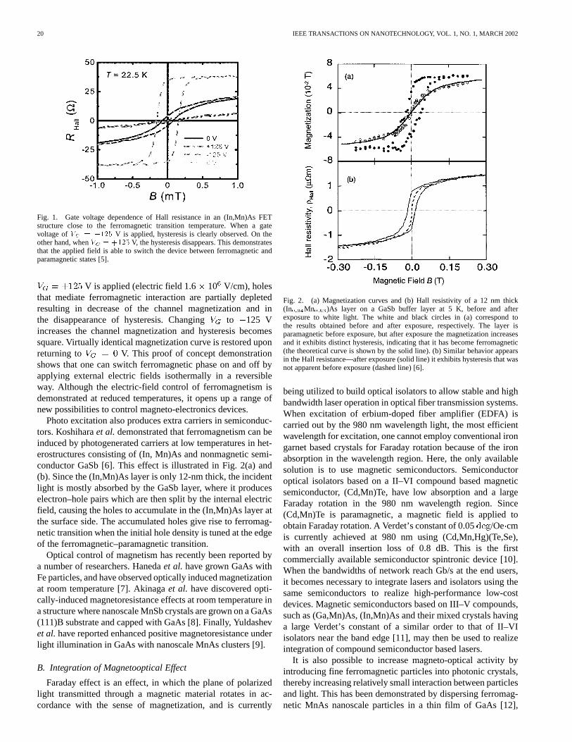
Photo excitation also produces extra carriers in semiconduc-tors. Koshiharaet al.demonstrated that ferromagnetism can beinduced by photogenerated carriers at low temperatures in het-erostructures consisting of (In, Mn)As and nonmagnetic semi-conductor GaSb [6]. This effect is illustrated in Fig. 2(a) and(b). Since the (In,Mn)As layer is only 12-nm thick, the incidentlight is mostly absorbed by the GaSb layer, where it produceselectron–hole pairs which are then split by the internal electricfield, causing the holes to accumulate in the (In,Mn)As layer atthe surface side. The accumulated holes give rise to ferromag-netic transition when the initial hole density is tuned at the edgeof the ferromagnetic–paramagnetic transition.
Optical control of magnetism has recently been reported bya number of researchers. Hanedaet al. have grown GaAs withFe particles, and have observed optically induced magnetizationat room temperature [7]. Akinagaet al. have discovered opti-cally-induced magnetoresistance effects at room temperature ina structure where nanoscale MnSb crystals are grown on a GaAs(111)B substrate and capped with GaAs [8]. Finally, Yuldashevet al.have reported enhanced positive magnetoresistance underlight illumination in GaAs with nanoscale MnAs clusters [9].
B. Integration of Magnetooptical Effect
Faraday effect is an effect, in which the plane of polarizedlight transmitted through a magnetic material rotates in ac-cordance with the sense of magnetization, and is currently
Fig. 2. (a) Magnetization curves and (b) Hall resistivity of a 12 nm thick(In Mn )As layer on a GaSb buffer layer at 5 K, before and afterexposure to white light. The white and black circles in (a) correspond tothe results obtained before and after exposure, respectively. The layer isparamagnetic before exposure, but after exposure the magnetization increasesand it exhibits distinct hysteresis, indicating that it has become ferromagnetic(the theoretical curve is shown by the solid line). (b) Similar behavior appearsin the Hall resistance—after exposure (solid line) it exhibits hysteresis that wasnot apparent before exposure (dashed line) [6].
being utilized to build optical isolators to allow stable and highbandwidth laser operation in optical fiber transmission systems.When excitation of erbium-doped fiber amplifier (EDFA) iscarried out by the 980 nm wavelength light, the most efficientwavelength for excitation, one cannot employ conventional irongarnet based crystals for Faraday rotation because of the ironabsorption in the wavelength region. Here, the only availablesolution is to use magnetic semiconductors. Semiconductoroptical isolators based on a II–VI compound based magneticsemiconductor, (Cd,Mn)Te, have low absorption and a largeFaraday rotation in the 980 nm wavelength region. Since(Cd,Mn)Te is paramagnetic, a magnetic field is applied toobtain Faraday rotation. A Verdet’s constant of 0.05/Oecmis currently achieved at 980 nm using (Cd,Mn,Hg)(Te,Se),with an overall insertion loss of 0.8 dB. This is the firstcommercially available semiconductor spintronic device [10].When the bandwidths of network reach Gb/s at the end users,it becomes necessary to integrate lasers and isolators using thesame semiconductors to realize high-performance low-costdevices. Magnetic semiconductors based on III–V compounds,such as (Ga,Mn)As, (In,Mn)As and their mixed crystals havinga large Verdet’s constant of a similar order to that of II–VIisolators near the band edge [11], may then be used to realizeintegration of compound semiconductor based lasers.
It is also possible to increase magneto-optical activity byintroducing fine ferromagnetic particles into photonic crystals,thereby increasing relatively small interaction between particlesand light. This has been demonstrated by dispersing ferromag-netic MnAs nanoscale particles in a thin film of GaAs [12],
AKINAGA AND OHNO: SEMICONDUCTOR SPINTRONICS 21
which is a part of an one-dimensional semiconductor photoniccrystal [13]. Model calculation has shown that the resultingFaraday effect is determined by the loss associated with theMnAs fine particles and the confinement of the electromagneticfield by the photonic crystal, and reduction of this loss iscritical in realizing Faraday rotation required for isolators.In addition, the control of waveguide mode by varying theexternal magnetic field has been demonstrated in a (Cd,Mn)Temagneto-optical waveguide on GaAs substrates [14].
C. Ultra High-Sensitive Magnetic Sensor
Rapid increase in the magnetic recording density of harddisk drives demands highly sensitive magnetic-field sensors.Magnetic nanostructures, such as metallic multilayers andtunnel junctions, show giant magnetoresistance (MR) effectand have already been used as a read head in currently availablehard disks [15] and [16]. All of them require nanometer ordercontrol of the constituent structures. For example, Giant MR(GMR) effect in metallic multilayers, so-called spin valveeffect, was enhanced by using NiO layers with the nanometerthickness [17]. Tunnel MR (TMR) up to 50% at room tem-perature was reported in a ferromagnetic tunnel junction ofTa (5 nm)–NiFe (3 nm)–Cu (20 nm)–NiFe (3 nm)–IrMn(10 nm)–CoFe (4 nm)–Al (0.8 nm)–Al(0.8nm)oxide–CoFe(4 nm)–NiFe (20 nm)–Ta (5 nm) [18].
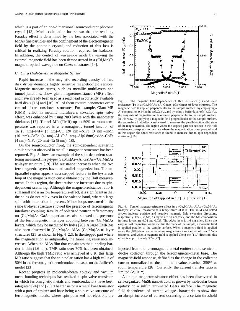
On the semiconductor front, the spin-dependent scatteringsimilar to that observed in metallic magnetic structures has beenreported. Fig. 3 shows an example of the spin-dependent scat-tering measured in a p-type (Ga,Mn)As–(Al,Ga)As–(Ga,Mn)Astri-layer structure [19]. The resistance increases when the twoferromagnetic layers have antiparallel magnetization. The an-tiparallel region appears as a stepped feature in the hysteresisloop of the magnetization curve obtained by the Hall measure-ments. In this region, the sheet resistance increases due to spin-dependent scattering. Although the magnetoresistance ratio isstill small and is an low temperature effect, it is significant in thatthe spins do not relax even in the valence band, where a largespin orbit interaction is present. Minor loops measured in thesame tri-layer structure showed the presence of ferromagneticinterlayer coupling. Results of polarized neutron reflectometryon (Ga,Mn)As–GaAs superlattices also showed the presenceof the ferromagnetic interlayer coupling between (Ga,Mn)Aslayers, which may be mediated by holes [20]. A large TMR hasalso been observed in (Ga,Mn)As–AlAs–(Ga,Mn)As tri-layerstructures [21] as shown in Fig. 4 [22]. In the stepped part wherethe magnetization is antiparallel, the tunneling resistance in-creases. When the AlAs film that constitutes the tunneling bar-rier is thin (1.6 nm), TMR ratio over 70% has been obtained.Although the high TMR ratio was achieved at 8 K, this largeMR ratio suggests that the spin polarization has a high value of50% in the ferromagnetic semiconductor, based on the Julliere’smodel [23].
Recent progress in molecular-beam epitaxy and vacuummetal bonding techniques has realized a spin-valve transistor,in which ferromagnetic metals and semiconductors have beenintegrated [24] and [25]. The transistor is a metal base transistorwith a part of emitter and base being a spin-valve structure offerromagnetic metals, where spin-polarized hot-electrons are
Fig. 3. The magnetic field dependence of Hall resistance (�) and sheetresistance () in a (Ga,Mn)As–(Al,Ga)As–(Ga,Mn)As tri-layer structure. Themagnetic field is applied perpendicular to the sample surface. By employing aAl composition 0.14 in the (Al,Ga)As, and by using a buffer layer of (In,Ga)As,the easy axis of magnetization is oriented perpendicular to the sample surface.In this way, by applying a magnetic field perpendicular to the sample surface,the anomalous Hall effect can be used to measure the parallel/antiparallel stateof the magnetization. The region where the stepped part can be seen in the Hallresistance corresponds to the state where the magnetization is antiparallel, andin this region the sheet resistance is found to increase due to spin-dependentscattering [19].
Fig. 4. Tunnel magnetoresistance effect in a (Ga,Mn)As–AlAs–(Ga,Mn)Astri-layer structure, measured at a temperature of 8 K. The solid and dottedarrows indicate positive and negative magnetic field sweeping directions,respectively. The (Ga,Mn)As layers are 50 nm thick, and the Mn compositionin these layers are 0.04 and 0.033. The AlAs layer is 1.6 nm thick. Since theeasy axis of magnetization lies within the plane of the sample, a magnetic fieldis applied parallel to the sample surface. When a magnetic field is appliedalong the [100] direction, a tunneling magnetoresistance effect of over 70% isobserved, and when a magnetic field is applied along the [110] direction, thiseffect is approximately 30% [22].
injected from the ferromagnetic–metal emitter to the semicon-ductor collector, through the ferromagnetic–metal base. Themagnetic-field response, defined as the change in the collectorcurrent normalized to the minimum value, reached 350% atroom temperature [26]. Currently, the current transfer ratio islimited ( 10 ).
A unique magnetoresistance effect has been discovered inself-organized MnSb nanostructures grown by molecular beamepitaxy on a sulfur terminated GaAs surface. The magneticfield dependence of current–voltage characteristics show thatan abrupt increase of current occurring at a certain threshold
22 IEEE TRANSACTIONS ON NANOTECHNOLOGY, VOL. 1, NO. 1, MARCH 2002
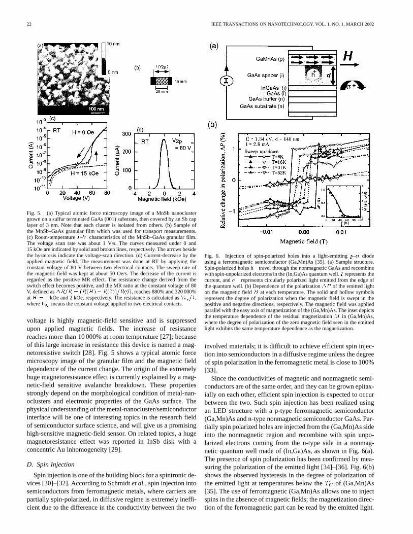
Fig. 5. (a) Typical atomic force microscopy image of a MnSb nanoclustergrown on a sulfur terminated GaAs (001) substrate, then covered by an Sb caplayer of 3 nm. Note that each cluster is isolated from others. (b) Sample ofthe MnSb–GaAs granular film which was used for transport measurements.(c) Room-temperatureI–V characteristics of the MnSb–GaAs granular film.The voltage scan rate was about 1 V/s. The curves measured under 0 and15 kOe are indicated by solid and broken lines, respectively. The arrows besidethe hysteresis indicate the voltage-scan direction. (d) Current-decrease by theapplied magnetic field. The measurement was done at RT by applying theconstant voltage of 80 V between two electrical contacts. The sweep rate ofthe magnetic field was kept at about 50 Oe/s. The decrease of the current isregarded as the positive MR effect. The resistance change derived from theswitch effect becomes positive, and the MR ratio at the constant voltage of 80V, defined as�R=R = (R(H)�R(0))=R(0), reaches 880% and 320 000%atH = 1 kOe and 2 kOe, respectively. The resistance is calculated asV =I ,whereV means the constant voltage applied to two electrical contacts.
voltage is highly magnetic-field sensitive and is suppressedupon applied magnetic fields. The increase of resistancereaches more than 10 000% at room temperature [27]; becauseof this large increase in resistance this device is named a mag-netoresistive switch [28]. Fig. 5 shows a typical atomic forcemicroscopy image of the granular film and the magnetic fielddependence of the current change. The origin of the extremelyhuge magnetoresistance effect is currently explained by a mag-netic-field sensitive avalanche breakdown. These propertiesstrongly depend on the morphological condition of metal-nan-oclusters and electronic properties of the GaAs surface. Thephysical understanding of the metal-nanocluster/semiconductorinterface will be one of interesting topics in the research fieldof semiconductor surface science, and will give us a promisinghigh-sensitive magnetic-field sensor. On related topics, a hugemagnetoresistance effect was reported in InSb disk with aconcentric Au inhomogeneity [29].
D. Spin Injection
Spin injection is one of the building block for a spintronic de-vices [30]–[32]. According to Schmidtet al., spin injection intosemiconductors from ferromagnetic metals, where carriers arepartially spin-polarized, in diffusive regime is extremely ineffi-cient due to the difference in the conductivity between the two
Fig. 6. Injection of spin-polarized holes into a light-emittingp–n diodeusing a ferromagnetic semiconductor (Ga,Mn)As [35]. (a) Sample structure.Spin-polarized holes h travel through the nonmagnetic GaAs and recombinewith spin-unpolarized electrons in the (In,Ga)As quantum well.I represents thecurrent, and� represents circularly polarized light emitted from the edge ofthe quantum well. (b) Dependence of the polarization�P of the emitted lighton the magnetic fieldB at each temperature. The solid and hollow symbolsrepresent the degree of polarization when the magnetic field is swept in thepositive and negative directions, respectively. The magnetic field was appliedparallel with the easy axis of magnetization of the (Ga,Mn)As. The inset depictsthe temperature dependence of the residual magnetizationM in (Ga,Mn)As,where the degree of polarization of the zero magnetic field seen in the emittedlight exhibits the same temperature dependence as the magnetization.
involved materials; it is difficult to achieve efficient spin injec-tion into semiconductors in a diffusive regime unless the degreeof spin polarization in the ferromagnetic metal is close to 100%[33].
Since the conductivities of magnetic and nonmagnetic semi-conductors are of the same order, and they can be grown epitax-ially on each other, efficient spin injection is expected to occurbetween the two. Such spin injection has been realized usingan LED structure with a p-type ferromagnetic semiconductor(Ga,Mn)As and n-type nonmagnetic semiconductor GaAs. Par-tially spin polarized holes are injected from the (Ga,Mn)As sideinto the nonmagnetic region and recombine with spin unpo-larized electrons coming from the n-type side in a nonmag-netic quantum well made of (In,Ga)As, as shown in Fig. 6(a).The presence of spin polarization has been confirmed by mea-suring the polarization of the emitted light [34]–[36]. Fig. 6(b)shows the observed hysteresis in the degree of polarization ofthe emitted light at temperatures below the of (Ga,Mn)As[35]. The use of ferromagnetic (Ga,Mn)As allows one to injectspins in the absence of magnetic fields; the magnetization direc-tion of the ferromagnetic part can be read by the emitted light.
AKINAGA AND OHNO: SEMICONDUCTOR SPINTRONICS 23
It is also possible to inject spin polarized electrons using bandtunneling [37] and [38]. An efficient spin injection is achievedby the use of a paramagnetic semiconductor [34] and [39].
Rashba pointed out that the use of tunnel junction for spin in-jection can overcome the difficulty associated with the diffusivetransport [40]. In the spin-valve transistor described above, thespin injection occurs as the nonequillibrium electrons (hot elec-trons) are injected into the semiconductor collector electrode.It has also been reported that by the use of a Schottky barrier,room temperature spin injection into an GaAs–(In,Ga)As LEDstructure is possible using an Fe electrode fabricated on the LEDstructure [41].
E. Control of Spin Polarization and Coherence
One of the great advantages of semiconductor spintronics isthat one can control spin relaxation time and spin-coherence ina wide range, from picoseconds to milliseconds. Very fast spinrelaxation can be used for optical gate switches, whereas longspin polarization opens up the possibility of utilizing spins asquantum bits for a quantum information processing.
Takeuchiet al. were the first to apply a circularly polarizedpump probe method to the measurement of spin relaxation insemiconductor quantum wells. They have shown that the spinrelaxation time of an AlGaAs–GaAs quantum well is 32 ps [42].When spin polarization is generated in a quantum well by an ex-ternal light, the absorption for right and left circularly polarizedlight differ as long as the polarization is present. By using thiseffect to extract optical signals only when spin polarization ispresent, very fast optically controlled gate switches can be con-structed. In particular, in quantum wells containing different Vatoms between barrier and well, such as InGaAs–InP quantumwells, the spin relaxation time is no more than a few picosec-onds at room temperature [43].
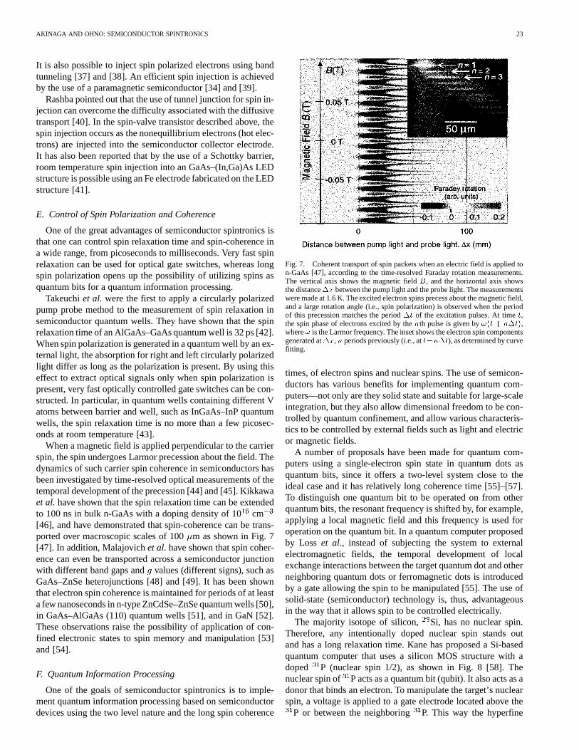
When a magnetic field is applied perpendicular to the carrierspin, the spin undergoes Larmor precession about the field. Thedynamics of such carrier spin coherence in semiconductors hasbeen investigated by time-resolved optical measurements of thetemporal development of the precession [44] and [45]. Kikkawaet al.have shown that the spin relaxation time can be extendedto 100 ns in bulk n-GaAs with a doping density of 10cm[46], and have demonstrated that spin-coherence can be trans-ported over macroscopic scales of 100m as shown in Fig. 7[47]. In addition, Malajovichet al.have shown that spin coher-ence can even be transported across a semiconductor junctionwith different band gaps andvalues (different signs), such asGaAs–ZnSe heterojunctions [48] and [49]. It has been shownthat electron spin coherence is maintained for periods of at leasta few nanoseconds in n-type ZnCdSe–ZnSe quantum wells [50],in GaAs–AlGaAs (110) quantum wells [51], and in GaN [52].These observations raise the possibility of application of con-fined electronic states to spin memory and manipulation [53]and [54].
F. Quantum Information Processing
One of the goals of semiconductor spintronics is to imple-ment quantum information processing based on semiconductordevices using the two level nature and the long spin coherence
Fig. 7. Coherent transport of spin packets when an electric field is applied ton-GaAs [47], according to the time-resolved Faraday rotation measurements.The vertical axis shows the magnetic fieldB, and the horizontal axis showsthe distance�x between the pump light and the probe light. The measurementswere made at 1.6 K. The excited electron spins precess about the magnetic field,and a large rotation angle (i.e., spin polarization) is observed when the periodof this precession matches the period�t of the excitation pulses. At timet,the spin phase of electrons excited by thenth pulse is given by!(t + n�t),where! is the Larmor frequency. The inset shows the electron spin componentsgenerated at�x,n periods previously (i.e., att�n�t), as determined by curvefitting.
times, of electron spins and nuclear spins. The use of semicon-ductors has various benefits for implementing quantum com-puters—not only are they solid state and suitable for large-scaleintegration, but they also allow dimensional freedom to be con-trolled by quantum confinement, and allow various characteris-tics to be controlled by external fields such as light and electricor magnetic fields.
A number of proposals have been made for quantum com-puters using a single-electron spin state in quantum dots asquantum bits, since it offers a two-level system close to theideal case and it has relatively long coherence time [55]–[57].To distinguish one quantum bit to be operated on from otherquantum bits, the resonant frequency is shifted by, for example,applying a local magnetic field and this frequency is used foroperation on the quantum bit. In a quantum computer proposedby Loss et al., instead of subjecting the system to externalelectromagnetic fields, the temporal development of localexchange interactions between the target quantum dot and otherneighboring quantum dots or ferromagnetic dots is introducedby a gate allowing the spin to be manipulated [55]. The use ofsolid-state (semiconductor) technology is, thus, advantageousin the way that it allows spin to be controlled electrically.
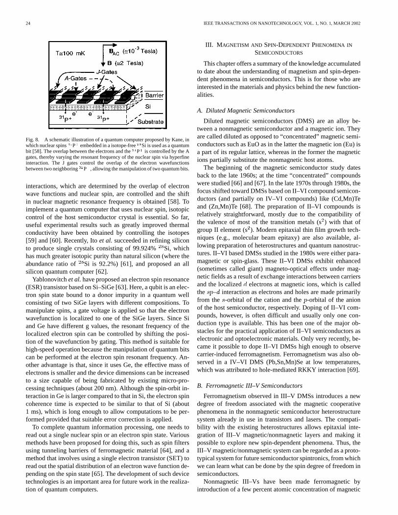
The majority isotope of silicon, Si, has no nuclear spin.Therefore, any intentionally doped nuclear spin stands outand has a long relaxation time. Kane has proposed a Si-basedquantum computer that uses a silicon MOS structure with adoped P (nuclear spin 1/2), as shown in Fig. 8 [58]. Thenuclear spin of P acts as a quantum bit (qubit). It also acts as adonor that binds an electron. To manipulate the target’s nuclearspin, a voltage is applied to a gate electrode located above the
P or between the neighboringP. This way the hyperfine
24 IEEE TRANSACTIONS ON NANOTECHNOLOGY, VOL. 1, NO. 1, MARCH 2002
Fig. 8. A schematic illustration of a quantum computer proposed by Kane, inwhich nuclear spins P embedded in a isotope-freeSi is used as a quantumbit [58]. The overlap between the electrons and theP is controlled by the Agates, thereby varying the resonant frequency of the nuclear spin via hyperfineinteraction. The J gates control the overlap of the electron wavefunctionsbetween two neighboring P , allowing the manipulation of two quantum bits.
interactions, which are determined by the overlap of electronwave functions and nuclear spin, are controlled and the shiftin nuclear magnetic resonance frequency is obtained [58]. Toimplement a quantum computer that uses nuclear spin, isotopiccontrol of the host semiconductor crystal is essential. So far,useful experimental results such as greatly improved thermalconductivity have been obtained by controlling the isotopes[59] and [60]. Recently, Itoet al. succeeded in refining siliconto produce single crystals consisting of 99.924%Si, whichhas much greater isotopic purity than natural silicon (where theabundance ratio of Si is 92.2%) [61], and proposed an allsilicon quantum computer [62].
Yablonovitchet al.have proposed an electron spin resonance(ESR) transistor based on Si–SiGe [63]. Here, a qubit is an elec-tron spin state bound to a donor impurity in a quantum wellconsisting of two SiGe layers with different compositions. Tomanipulate spins, a gate voltage is applied so that the electronwavefunction is localized to one of the SiGe layers. Since Siand Ge have different g values, the resonant frequency of thelocalized electron spin can be controlled by shifting the posi-tion of the wavefunction by gating. This method is suitable forhigh-speed operation because the manipulation of quantum bitscan be performed at the electron spin resonant frequency. An-other advantage is that, since it uses Ge, the effective mass ofelectrons is smaller and the device dimensions can be increasedto a size capable of being fabricated by existing micro-pro-cessing techniques (about 200 nm). Although the spin-orbit in-teraction in Ge is larger compared to that in Si, the electron spincoherence time is expected to be similar to that of Si (about1 ms), which is long enough to allow computations to be per-formed provided that suitable error correction is applied.
To complete quantum information processing, one needs toread out a single nuclear spin or an electron spin state. Variousmethods have been proposed for doing this, such as spin filtersusing tunneling barriers of ferromagnetic material [64], and amethod that involves using a single electron transistor (SET) toread out the spatial distribution of an electron wave function de-pending on the spin state [65]. The development of such devicetechnologies is an important area for future work in the realiza-tion of quantum computers.
III. M AGNETISM AND SPIN-DEPENDENTPHENOMENA IN
SEMICONDUCTORS
This chapter offers a summary of the knowledge accumulatedto date about the understanding of magnetism and spin-depen-dent phenomena in semiconductors. This is for those who areinterested in the materials and physics behind the new function-alities.
A. Diluted Magnetic Semiconductors
Diluted magnetic semiconductors (DMS) are an alloy be-tween a nonmagnetic semiconductor and a magnetic ion. Theyare called diluted as opposed to “concentrated” magnetic semi-conductors such as EuO as in the latter the magnetic ion (Eu) isa part of its regular lattice, whereas in the former the magneticions partially substitute the nonmagnetic host atoms.
The beginning of the magnetic semiconductor study datesback to the late 1960s; at the time “concentrated” compoundswere studied [66] and [67]. In the late 1970s through 1980s, thefocus shifted toward DMSs based on II–VI compound semicon-ductors (and partially on IV–VI compounds) like (Cd,Mn)Teand (Zn,Mn)Te [68]. The preparation of II–VI compounds isrelatively straightforward, mostly due to the compatibility ofthe valence of most of the transition metals (s) with that ofgroup II element (s). Modern epitaxial thin film growth tech-niques (e.g., molecular beam epitaxy) are also available, al-lowing preparation of heterostructures and quantum nanostruc-tures. II–VI based DMSs studied in the 1980s were either para-magnetic or spin-glass. These II–VI DMSs exhibit enhanced(sometimes called giant) magneto-optical effects under mag-netic fields as a result of exchange interactions between carriersand the localized electrons at magnetic ions, which is calledthe – interaction as electrons and holes are made primarilyfrom the -orbital of the cation and the-orbital of the anionof the host semiconductor, respectively. Doping of II–VI com-pounds, however, is often difficult and usually only one con-duction type is available. This has been one of the major ob-stacles for the practical application of II–VI semiconductors aselectronic and optoelectronic materials. Only very recently, be-came it possible to dope II–VI DMSs high enough to observecarrier-induced ferromagnetism. Ferromagnetism was also ob-served in a IV–VI DMS (Pb,Sn,Mn)Se at low temperatures,which was attributed to hole-mediated RKKY interaction [69].
B. Ferromagnetic III–V Semiconductors
Ferromagnetism observed in III–V DMSs introduces a newdegree of freedom associated with the magnetic cooperativephenomena in the nonmagnetic semiconductor heterostructuresystem already in use in transistors and lasers. The compati-bility with the existing heterostructures allows epitaxial inte-gration of III–V magnetic/nonmagnetic layers and making itpossible to explore new spin-dependent phenomena. Thus, theIII–V magnetic/nonmagnetic system can be regarded as a proto-typical system for future semiconductor spintronics, from whichwe can learn what can be done by the spin degree of freedom insemiconductors.
Nonmagnetic III–Vs have been made ferromagnetic byintroduction of a few percent atomic concentration of magnetic
AKINAGA AND OHNO: SEMICONDUCTOR SPINTRONICS 25
ions, which exceeds by far the equilibrium solubility in III–Vsemiconductors. In 1989, Munekataet al.used low-temperaturemolecular beam epitaxy (LT-MBE; deposition temperatureapprox. 250 C) and succeeded in suppressing the surfacesegregation and formation of second phases, resulting in epi-taxial growth of a metastable alloy of InAs and Mn, (In,Mn)As[70]. Three years later ferromagnetism was reported in p-type(In,Mn)As [71], and in 1996 the growth of (Ga,Mn)As [72]—aGaAs-based DMS—and ferromagnetic transitions in p-type(Ga,Mn)As were reported [73]. The highest ferromagnetictransition temperature of (Ga,Mn)As obtained so far is110 K (Mn concentration ) [74]. Since (Ga,Mn)Ascan be epitaxially grown on a GaAs substrate, it is compatiblewith GaAs–(Al,Ga)As quantum structures, making it an indis-pensable material for the study of semiconductor spintronics[75]–[77].
1) Magnetic Properties:The easy axis of magnetizationin (Ga,Mn)As grown on GaAs (001) planes is oriented withinthe plane due to lattice strain [73]. The lattice constant of(Ga,Ma)As is slightly larger than that of GaAs resultingin compressive strain in the epitaxial layer. This easy axisorientation can be made perpendicular to the epitaxial filmwhen the sign of strain is reversed; this is possible by intro-duction of a lattice relaxed (In,Ga)As buffer layer with largerlattice constant than the (Ga,Mn)As layer grown on top ofit [78]. Stripe shape magnetic domain has been observed, inaccordance with the conventional theory, in (Ga,Mn)As with aperpendicular-to-the-plane easy axis [79].
The ferromagnetic transition temperature,, can be deter-mined in a number of ways: 1) the temperature dependence ofremanent magnetization; 2) an Arrott plot ( plot)using the magnetic field dependence of the magnetization nearthe transition temperature; or 3) a Curie–Weiss plot of the mag-netic susceptibility in the high-temperature paramagnetic re-gion. These methods all produce almost the same[81]. Therelationship between and is K up to around
, and further increase of results in decrease of[74]. Increase of up to 110 K by an thermal annealing wasalso demonstrated in (Ga,Mn)As without changing[81] and[82]. The defect structure seems to play a role in this result, butthe detail has not yet been fully understood. Efforts to increase
beyond 110 K in (Ga,Mn)As have so far been unsuccessful;the maximum that (In,Mn)As exhibits is 50 K [83].
2) Mechanism Leading to Ferromagnetism:A model of car-rier-induced ferromagnetism has been developed and shownto explain the experimentally observed features, especiallyand its chemical trend. This mean field model assumes twospin subsystems, carrier spins and localized spins at magneticions, interacting through the exchange interaction (the– in-teraction). Having a nonzero magnetization increases the freeenergy of the localized spin system, but reduces the energy ofthe carrier systems via spin-splitting of the bands (no energygain if no carriers are present). The free energy penalty reducesas temperature is reduces and balances with the energy gain ofthe carrier system at [84]. This is known as the Zenerferromagnetism [85], which Zener himself later abandoned asin metals oscillatory interaction has to be taken into accountdue to high carrier concentration. Note that this Zener ferro-
magnetism is different from Zener’s famous double exchangeinteraction.
Following the prescription, one can calculatefor a numberof compounds. A 6 6 Luttinger–Kohn Hamiltonian wasused, where– interactions were taken into account, to calcu-late the carrier energy in the valence band. Only valence bandwas dealt with as (Ga,Mn)As is heavily p-type. For (Ga,Mn)As,the parameters of GaAs and a value of eV wereused. The latter was obtained from the core-level photoemissionspectroscopy and modeling ( is the density of cation sites,and is the – exchange integral) [86]. An enhancement factorof 1.2 was included to account for the effect of carrier–carrierinteraction [87]. The calculated for (Ga,Mn)As, (In,Mn)As,and (Zn,Mn)Te all agree well with the experimental values. Thismodel also explains the absence of ferromagnetism in n-typematerials, which is because of the small exchange interactionin the conduction band; the– interaction is eV(where is the – exchange integral). The strain dependenteasy axis of magnetization as well as the peculiar temperaturedependence of magnetic circular dichroism in (Ga,Mn)As [88]are also explained by the model [89]. It has been pointed out,however, that other factors such as low energy spin-wave exci-tation and disorder must be considered [90] and [91].
By first principle electronic structure calculation, Akaishowed that when holes are present, a half-metallic ferro-magnetic state becomes stable in (In,Mn)As. He discussedthe ferromagnetism being as a result of double exchangeinteractions caused by hopping ofholes [92]. First principlecalculation also has shown that the ferromagnetic state is stablein a hypothetical zincblende GaAs–MnAs superlattice, wherehalf-metallic state is predicted [93]. The double resonancemechanism has been proposed for the ferromagnetism of(Ga,Mn)As [94]. A large effort is currently being devoted tothe understanding of ferromagnetism observed in transitionmetal doped semiconductors and we are witnessing a very rapidprogresses in this theoretical area of research [95] and [96].
C. II–VI and Other Ferromagnetic Semiconductors
Advances in techniques for doping in II–VI semiconductorshave made it possible to achieve carrier densities in excessof 10 cm [97]. Shortly after a theory of ferromagnetictransition based on– exchange interactions was put forward[98], ferromagnetism was observed below 1.8 K in modulationdoped (Cd Mn )Te quantum well (8 nm, 2 10cm ) [99]. Ferromagnetism has also been observed in a thinfilm (500 nm thick) of (Zn Mn )Te and (Be Mn )Te(where ) with – cm (K) [100], [101], [102]. Room temperature ferromagnetismhas been reported recently in a number of nonconventionalmagnetic semiconductors, 320 K in a II–IV–Vchalcopyrite(Cd Mn )GeP [103], 290–380 K in (Zn,Co)O [104],room-temperature ferromagnetism in TiO: Co [105] and[106]. Sonodaet al. have recently succeeded in synthesizing(Ga,Mn)N showing ferromagnetic behavior at and beyond roomtemperature [107]; ferromagnetism in (Ga,Mn)N has been alsoreported by other groups [108] and [109]. The first observationof a ferromagnetic transition in a group-IV semiconductor hasalso been reported in Mn-doped Ge quite recently [110].
26 IEEE TRANSACTIONS ON NANOTECHNOLOGY, VOL. 1, NO. 1, MARCH 2002
D. Nonmagnetic Semiconductors
Along with the developments of ferromagnetic semiconduc-tors, numerous progresses in understanding and manipulatingspin properties in nonmagnetic semiconductor structures havealso been made over the last decade.
Carrier spin relaxation in semiconductors has been studiedboth theoretically and experimentally [111]. Time resolved laserspectroscopy of spin relaxation times in semiconductor struc-tures have revealed that the major spin relaxation mechanismsinclude spin-orbit interactions originating from the lack of theinversion symmetry (the D’yakonov–Perel’ effect), band mixing(the Elliott–Yafet effect), and electron–hole exchange interac-tion (the Bir–Aronov–Pikus effect) [111]. The relative impor-tance among these mechanisms depends on material properties(the spin-orbit coupling and the fundamental band gap) and onparameters as dimension, temperature, kinetic energy, scatteringtime, and doping.
In quantum nanostructures, the degeneracy of light andheavy holes is lifted, and it is, thus, possible to achieve 100%spin-polarized carriers by resonant excitation of electron-heavyhole exciton with circularly polarized light. The introduction ofquantum confinement also modifies mobility [112], symmetry[113]–[115], excitonic effects [116], locality [117], and doping[118], all resulting in modification of the spin relaxationprocesses. In GaAs, for example, the reported electron spinrelaxation times are distributed over a wide range from a fewpicoseconds to several tens of nanoseconds [119]. In particular,the D’yakonov–Perel’ effect dominant at room temperaturedepends strongly on the crystallographic orientation of thegrowth direction [115].
In quantum dots where the electron transport is dominatedby the Coulomb blockade, it is possible to control the numberof occupying electrons (even or odd) by varying the gate voltage[120]. In such few electron systems, spin (magnetism) plays apredominant role in the transport properties via exchange in-teraction. This behavior is expected to prove useful for func-tions such as spin filters and spin memories [121] and [122].Exchange interactions between a quantum dot with a controlledspin state and an electrode (the Kondo effect) have also beenobserved [123] and [124].
To design and to implement solid-state quantum informa-tion processing that uses nuclear spin as a quantum bit, it isnecessary to clarify the dynamics of interaction between elec-tron spin and nuclear spin. So far, in semiconductors and itsquantum structures, electron spin polarization have been mea-sured to investigate the hyperfine interaction involving the Over-hauser effect and the Hanle effect [111], [125], [126], and overthe last few years more light has been shed on the dynamics ofthe Overhauser effect from the time-resolved pump–probe mea-surements [127]–[129].
IV. SEMICONDUCTORSPINTRONICSCHALLENGES
This final section summarizes a set of challenges that has tobe met in order to materialize the advantages and opportunitiesoffered by semiconductor spintronics. There are two directionsfor semiconductor spintronics; one is semiconductor magne-toelectronics, where magnetization direction is important, and
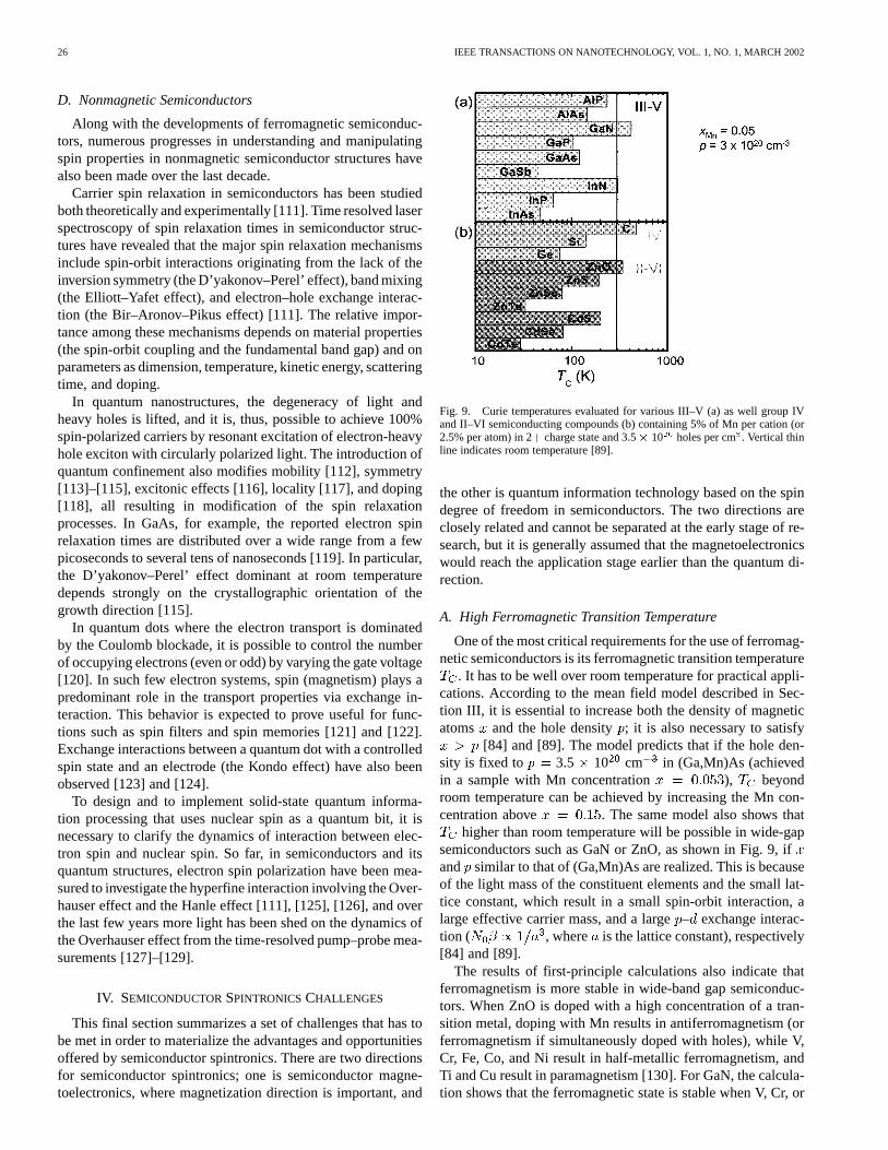
Fig. 9. Curie temperatures evaluated for various III–V (a) as well group IVand II–VI semiconducting compounds (b) containing 5% of Mn per cation (or2.5% per atom) in 2+ charge state and 3.5� 10 holes per cm. Vertical thinline indicates room temperature [89].
the other is quantum information technology based on the spindegree of freedom in semiconductors. The two directions areclosely related and cannot be separated at the early stage of re-search, but it is generally assumed that the magnetoelectronicswould reach the application stage earlier than the quantum di-rection.
A. High Ferromagnetic Transition Temperature
One of the most critical requirements for the use of ferromag-netic semiconductors is its ferromagnetic transition temperature
. It has to be well over room temperature for practical appli-cations. According to the mean field model described in Sec-tion III, it is essential to increase both the density of magneticatoms and the hole density; it is also necessary to satisfy
[84] and [89]. The model predicts that if the hole den-sity is fixed to 3.5 10 cm in (Ga,Mn)As (achievedin a sample with Mn concentration ), beyondroom temperature can be achieved by increasing the Mn con-centration above . The same model also shows that
higher than room temperature will be possible in wide-gapsemiconductors such as GaN or ZnO, as shown in Fig. 9, ifand similar to that of (Ga,Mn)As are realized. This is becauseof the light mass of the constituent elements and the small lat-tice constant, which result in a small spin-orbit interaction, alarge effective carrier mass, and a large– exchange interac-tion ( , where is the lattice constant), respectively[84] and [89].
The results of first-principle calculations also indicate thatferromagnetism is more stable in wide-band gap semiconduc-tors. When ZnO is doped with a high concentration of a tran-sition metal, doping with Mn results in antiferromagnetism (orferromagnetism if simultaneously doped with holes), while V,Cr, Fe, Co, and Ni result in half-metallic ferromagnetism, andTi and Cu result in paramagnetism [130]. For GaN, the calcula-tion shows that the ferromagnetic state is stable when V, Cr, or
AKINAGA AND OHNO: SEMICONDUCTOR SPINTRONICS 27
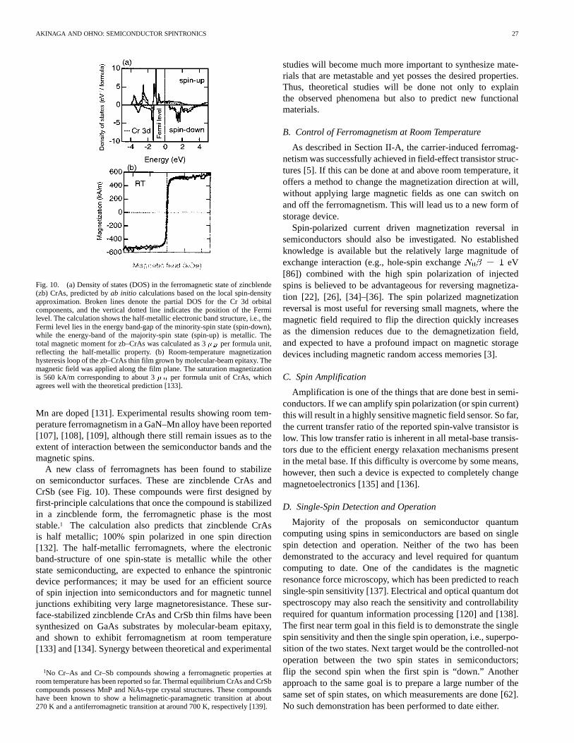
Fig. 10. (a) Density of states (DOS) in the ferromagnetic state of zincblende(zb) CrAs, predicted byab initio calculations based on the local spin-densityapproximation. Broken lines denote the partial DOS for the Cr 3d orbitalcomponents, and the vertical dotted line indicates the position of the Fermilevel. The calculation shows the half-metallic electronic band structure, i.e., theFermi level lies in the energy band-gap of the minority-spin state (spin-down),while the energy-band of the majority-spin state (spin-up) is metallic. Thetotal magnetic moment for zb–CrAs was calculated as 3� per formula unit,reflecting the half-metallic property. (b) Room-temperature magnetizationhysteresis loop of the zb–CrAs thin film grown by molecular-beam epitaxy. Themagnetic field was applied along the film plane. The saturation magnetizationis 560 kA/m corresponding to about 3� per formula unit of CrAs, whichagrees well with the theoretical prediction [133].
Mn are doped [131]. Experimental results showing room tem-perature ferromagnetism in a GaN–Mn alloy have been reported[107], [108], [109], although there still remain issues as to theextent of interaction between the semiconductor bands and themagnetic spins.
A new class of ferromagnets has been found to stabilizeon semiconductor surfaces. These are zincblende CrAs andCrSb (see Fig. 10). These compounds were first designed byfirst-principle calculations that once the compound is stabilizedin a zincblende form, the ferromagnetic phase is the moststable.1 The calculation also predicts that zincblende CrAsis half metallic; 100% spin polarized in one spin direction[132]. The half-metallic ferromagnets, where the electronicband-structure of one spin-state is metallic while the otherstate semiconducting, are expected to enhance the spintronicdevice performances; it may be used for an efficient sourceof spin injection into semiconductors and for magnetic tunneljunctions exhibiting very large magnetoresistance. These sur-face-stabilized zincblende CrAs and CrSb thin films have beensynthesized on GaAs substrates by molecular-beam epitaxy,and shown to exhibit ferromagnetism at room temperature[133] and [134]. Synergy between theoretical and experimental
1No Cr–As and Cr–Sb compounds showing a ferromagnetic properties atroom temperature has been reported so far. Thermal equilibrium CrAs and CrSbcompounds possess MnP and NiAs-type crystal structures. These compoundshave been known to show a helimagnetic-paramagnetic transition at about270 K and a antiferromagnetic transition at around 700 K, respectively [139].
studies will become much more important to synthesize mate-rials that are metastable and yet posses the desired properties.Thus, theoretical studies will be done not only to explainthe observed phenomena but also to predict new functionalmaterials.
B. Control of Ferromagnetism at Room Temperature
As described in Section II-A, the carrier-induced ferromag-netism was successfully achieved in field-effect transistor struc-tures [5]. If this can be done at and above room temperature, itoffers a method to change the magnetization direction at will,without applying large magnetic fields as one can switch onand off the ferromagnetism. This will lead us to a new form ofstorage device.
Spin-polarized current driven magnetization reversal insemiconductors should also be investigated. No establishedknowledge is available but the relatively large magnitude ofexchange interaction (e.g., hole-spin exchange eV[86]) combined with the high spin polarization of injectedspins is believed to be advantageous for reversing magnetiza-tion [22], [26], [34]–[36]. The spin polarized magnetizationreversal is most useful for reversing small magnets, where themagnetic field required to flip the direction quickly increasesas the dimension reduces due to the demagnetization field,and expected to have a profound impact on magnetic storagedevices including magnetic random access memories [3].
C. Spin Amplification
Amplification is one of the things that are done best in semi-conductors. If we can amplify spin polarization (or spin current)this will result in a highly sensitive magnetic field sensor. So far,the current transfer ratio of the reported spin-valve transistor islow. This low transfer ratio is inherent in all metal-base transis-tors due to the efficient energy relaxation mechanisms presentin the metal base. If this difficulty is overcome by some means,however, then such a device is expected to completely changemagnetoelectronics [135] and [136].
D. Single-Spin Detection and Operation
Majority of the proposals on semiconductor quantumcomputing using spins in semiconductors are based on singlespin detection and operation. Neither of the two has beendemonstrated to the accuracy and level required for quantumcomputing to date. One of the candidates is the magneticresonance force microscopy, which has been predicted to reachsingle-spin sensitivity [137]. Electrical and optical quantum dotspectroscopy may also reach the sensitivity and controllabilityrequired for quantum information processing [120] and [138].The first near term goal in this field is to demonstrate the singlespin sensitivity and then the single spin operation, i.e., superpo-sition of the two states. Next target would be the controlled-notoperation between the two spin states in semiconductors;flip the second spin when the first spin is “down.” Anotherapproach to the same goal is to prepare a large number of thesame set of spin states, on which measurements are done [62].No such demonstration has been performed to date either.
28 IEEE TRANSACTIONS ON NANOTECHNOLOGY, VOL. 1, NO. 1, MARCH 2002
V. CONCLUSION
We have attempted to review the recent progresses achievedin the field of semiconductor spintronics, where research aredirected toward realizing functionalities by the use of bothcharge and spin degrees of freedom in semiconductors. Over thelast 10 years, significant developments have been made in thisfield. We now have in our hand a number of prototypical systemsranging from ferromagnetic semiconductor heterostructures tolong spatiotemporal spin coherence in nonmagnetic heterostruc-tures. Working on these structures, we are learning, not onlyby theory but also by experiment, what are available to us insemiconductors by using the largely unexplored spin degree offreedom. The progress in room-temperature ferromagnetismin semiconductors will certainly make semiconductor magne-toelectronics possible and the long spin coherence time andlength together with the various means of control and couplingto optics make spins in semiconductors a strong candidate forrealizing future quantum information technology. Althoughsemiconductor spintronics has begun to make progress, makingit into real “electronics” requires a comprehensive and dynamicresearch and development program involving researchers froma broad spectrum of fields ranging from solid-state physics,crystal growth, magnetism, electrical and computer engineering,circuit design, and information science. Establishing links withresearchers in other fields is becoming vitally important, andwe invite you to join this exciting emerging field.
ACKNOWLEDGMENT
The authors would like to thank F. Matsukura, Y. Ohno,K. Ono, M. Oshima, M. Shirai, and T. Manago for theirvaluable discussion.
REFERENCES
[1] H. Ohno, “Making nonmagnetic semiconductor ferromagnetic,”Science, vol. 281, pp. 951–956, 1998.
[2] H. Ohno, F. Matsukura, and Y. Ohno, “Semiconductor spin electronics,”Jpn. Soc. Appl. Phys. Int., vol. 4, no. 5, pp. 4–13, 2002. [Online]. Avail-able: http://www.jsapi.jsap.or.jp/.
[3] S. Wolf, D. D. Awschalom, R. A. Buhrman, J. M. Daughton, S. vonMolnar, M. L. Roukes, A. Y. Chtchelkanova, and D. M. Treger, “Spin-tronics: A spin-based electronics vision for the future,”Science, vol. 294,pp. 1488–1495, 2001.
[4] M. R. Freeman and B. C. Choi, “Advances in magnetic microscopy,”Science, vol. 294, pp. 1484–1488, 2001.
[5] H. Ohno, D. Chiba, F. Matsukura, T. Omiya, E. Abe, T. Dietl, Y. Ohno,and K. Ohtani, “Electric-field control of ferromagnetism,”Nature, vol.408, pp. 944–946, 2000.
[6] S. Koshihara, A. Oiwa, M. Hirasawa, S. Katsumoto, Y. Iye, C. Urano,H. Takagi, and H. Munekata, “Ferromagnetic order induced by photo-generated carriers in magnetic III-IV semiconductor heterostructures of(In,Mn)As–GaSb,”Phys. Rev. Lett., vol. 78, pp. 4617–4620, 1997.
[7] S. Haneda, H. Munekata, Y. Takatani, and S. Koshihara, “Fe-basedmagnetic-semiconductor hyhrid structures for photocarrier-inducedmagnetism,”J. Appl. Phys., vol. 87, pp. 6445–6447, 2000.
[8] H. Akinaga, M. Mizuguchi, K. Ono, and M. Oshima, “Room-temper-ature photoinduced magnetoresistance effect in GaAs including MnSbnanomagnets,”Appl. Phys. Lett., vol. 76, pp. 2600–2602, 2000.
[9] Sh. U. Yuldashev, Y. Shon, Y. H. Kwon, D. J. Fu, D. Y. Kim, H. J. Kim,T. W. Kang, and X. Fan, “Enhanced positive magnetoresistance effectin GaAs with nanoscale magnetic clusters,”J. Appl. Phys., vol. 90, pp.3004–3306, 2001.
[10] K. Onodera, “Optical devices using diluted magnetic semiconductorswith a large Faraday effect” (in Japanese),Material Integration, vol. 13,pp. 57–60, 2000.
[11] T. Kuroiwa, T. Yasuda, F. Matsukura, A. Shen, Y. Ohno, Y. Segawa,and H. Ohno, “Faraday rotation of ferromagnetic (Ga,Mn)As,”Electron.Lett., vol. 34, pp. 190–192, 1998.
[12] H. Akinaga, S. Miyanishi, K. Tanaka, W. Van Roy, and K. Onodera,“magnetooptical properties and the potential application of GaAs withmagnetic MnAs nanocolusters,”Appl. Phys. Lett., vol. 76, pp. 97–99,2000.
[13] H. Shimizu, M. Miyamura, and M. Tanaka, “Enhanced magnetoopticaleffect in a GaAs:MnAs nanoscale hybrid structure combined withGaAs–AlAs distributed Bragg reflectors,”J. Vac. Sci. Technol., vol. B18, pp. 2063–2065, 2000.
[14] W. Zaets and K. Ando, “Magnetooptical mode conversion inCd Mn Te waveguide on GaAs substrate,”Appl. Phys. Lett., vol.77, pp. 1593–1595, 2000.
[15] M. N. Baibich, J. M. Broto, A. Fert, F. Nguyen Van Dau, F. Petroff, P.Eitenne, G. Creuzet, A. Friederich, and J. Chazelas, “Giant magnetore-sistance of (001)Fe–(001)Cr magnetic superlattices,”Phys. Rev. Lett.,vol. 61, pp. 2472–2475, 1988.
[16] T. Miyazaki and N. Tezuka, “Giant magnetic tunneling effect in Fe�Al O �Fe junction,”J. Magn. Magn. Mater., vol. 139, pp. L231–L234,1995.
[17] W. F. Egelhoff, Jr., T. Ha, R. D. K. Misra, Y. Kadmon, J. Nir, C. J. Powell,M. D. Stiles, R. D. McMichael, C.-L. Lin, J. M. Sivertsen, J. H. Judy, K.Takano, A. E. Berkowitz, T. C. Anthony, and J. A. Brug, “Magnetoresis-tance values exceeding 21% in symmetric spin valves,”J. Appl. Phys.,vol. 78, pp. 273–277, 1995.
[18] X. F. Han, T. Daibou, M. Kamijo, K. Yaoita, H. Kubota, Y. Ando, andT. Miyazaki, “High-magnetoresistance tunnel junctions using CoFeferromagnetic electrodes,”Jpn. J. Appl. Phys., vol. 39, pp. L439–L441,2000.
[19] N. Akiba, D. Chiba, K. Nakata, F. Matsukura, Y. Ohno, and H.Ohno, “Spin-dependent scattering in semiconducting ferromagnetic(Ga,Mn)As trilayer structures,”J. Appl. Phys., vol. 87, pp. 6436–6438,2000.
[20] H. Kêpa, J. Kunter-Pielaszek, A. Twardowski, C. F. Majkrzak, J. Sad-owski, T. Story, and T. M. Giebultowicz, “Ferromagnetism of GaMsAsstudied by polarized neutron reflectometry,”Phys. Rev., vol. B 64, p.121 302 (R), 2001.
[21] D. Chiba, N. Akiba, F. Matsukura, Y. Ohno, and H. Ohno, “Magnetore-sistance effect and interlayer coupling of (Ga,Mn)As trilayer structures,”Appl. Phys. Lett., vol. 77, pp. 1873–1875, 2000.
[22] M. Tanaka and Y. Higo, “Large tunneling magnetoresistance inGaMnAs-AlAs-GaMnAs ferromagnetic semiconductor tunnel junc-tions,” Phys. Rev. Lett., vol. 87, p. 26 602, 2001.
[23] M. Julliere, “Tunneling between ferromagnetic films,”Phys. Lett., vol.54A, pp. 225–226, 1975.
[24] D. J. Monsma, R. Vlutters, and J. C. Lodder, “Room temperature-oper-ating spin-valve transistors formed by vacuum bonding,”Science, vol.281, pp. 407–409, 1998.
[25] R. Sato and K. Mizushima, “Spin-valve transistor with anFe-Au-Fe(001) base,”Appl. Phys. Lett., vol. 79, pp. 1157–1159,2001.
[26] R. Jansen, P. S. Anil Kumar, O. M. J. Van’t Erve, R. Vlutters, P. de Haan,and J. C. Lodder, “Thermal spin-wave scattering in hot-electron magne-totransport across a spin valve,”Phys. Rev. Lett., vol. 85, pp. 3277–3280,2000.
[27] M. Mizuguchi, H. Akinaga, K. Ono, and M. Oshima, “Magnetic proper-ties of MnSb granular films,”J. Magn. Magn. Mater., vol. 226-230, pp.1838–1839, 2001.
[28] H. Akinaga, M. Mizuguchi, K. Ono, and M. Oshima, “Room-temper-ature thousandfold magnetoresistance change in MnSb granular films:Magnetoresistive switch effect,”Appl. Phys. Lett., vol. 76, pp. 357–359,2000.
[29] S. A. Solin, T. Thio, D. R. Hines, and J. J. Heremans, “En-hanced room-temperature geometric magnetoresistance in inhomoge-neous narrow-gap semiconductors,”Science, vol. 289, pp. 1530–1532,2000.
[30] P. R. Hammar, B. R. Bennet, M. J. Yang, and M. Johnson, “Observationof spin injection at a ferromagnet-semiconductor interface,”Phys. Rev.Lett., vol. 83, pp. 203–206, 1999.
[31] F. G. Monzon and M. L. Roukes, “Spin injection and the local Hall ef-fect in InAs quantum wells,”J. Magn. Magn. Mater., vol. 198/199, pp.632–635, 1999.
[32] J. Nitta, C.-M. Hu, A. Jensen, J. B. Hansen, and H. Takayanagi, “Spin in-jection and detection experiment in a two dimensional electron gas withinter-digital-ferromagnetic contacts,”Physica, vol. E 10, pp. 467–471,2001.
AKINAGA AND OHNO: SEMICONDUCTOR SPINTRONICS 29
[33] G. Schmidt, D. Ferrand, L. W. Molenkamp, A. T. Filip, and B. J. vanWees, “Fundamental obstacle for electrical spin injection from a ferro-magnetic metal into a diffusive semiconductor,”Phys. Rev., vol. B 62,pp. R4790–R4793, 2000.
[34] R. Fiederling, M. Keim, G. Reuscher, W. Ossau, G. Schmidt, A. Waag,and L. W. Molenkamp, “Injection and detection of a spin-polarized cur-rent in a light-emitting diode,”Nature, vol. 402, pp. 787–790, 1999.
[35] Y. Ohno, D. K. Young, B. Beschoten, F. Matsukura, H. Ohno, and D. D.Awschalom, “Electrical spin injection in a ferromagnetic semiconductorheterostructure,”Nature, vol. 402, pp. 790–792, 1999.
[36] B. T. Jonker, Y. D. Park, B. R. Bennett, H. D. Cheong, G. Kioseoglou,and A. Petrou, “Robust electrical spin injection into a semiconductorheterostructure,”Phys. Rev., vol. B 62, pp. 8180–8183, 2000.
[37] M. Kohda, Y. Ohno, K. Takamura, F. Matsukura, and H. Ohno, “A spinEsaki diode,”Jpn. J. Appl. Phys., vol. 40, pp. L1274–L1276, 2001.
[38] E. Johnston-Halperin, D. Lofgreen, R. K. Kawakami, D. K. Young, L.Coldren, A. C. Gossard, and D. D. Awschalom, “Spin-polarized Zenertunneling in (Ga,Mn)As,”Phys. Rev., vol. B 65, p. 041 306, 2002.
[39] M. Oestreich, J. Hubner, D. Hagele, P. J. Klar, W. Heimbrodt, W. W.Ruhle, D. E. Ashenford, and B. Lunn, “Spin injection into semiconduc-tors,” Appl. Phys. Lett., vol. 74, pp. 1251–1253, 1999.
[40] E. I. Rashba, “Theory of electrical spin injection: Tunnel contacts as asolution of the conductivity mismatch problem,”Phys. Rev., vol. B 62,pp. R16267–R16270, 2000.
[41] H. J. Zhu, M. Ramsteiner, H. Kostial, M. Wassermeier, H.-P. Schonherr,and K. H. Ploog, “Room-temperature spin injection from Fe into GaAs,”Phys. Rev. Lett., vol. 87, p. 016 601, 2001.
[42] A. Tackeuchi, S. Muto, T. Inata, and T. Fujii, “Direct observation ofpicosecond spin relaxation of excitons in GaAs–AlGaAs quantum wellsusing spin-dependent optical nonlinearity,”Appl. Phys. Lett., vol. 56, pp.2213–2215, 1990.
[43] A. Tackeuchi, O. Wada, and Y. Nishikawa, “Electron spin relaxationin InGaAs–InP multiple-quantum wells,”Appl. Phys. Lett., vol. 70, pp.1131–1133, 1997.
[44] A. P. Heberle, W. W. Ruhle, and K. Ploog, “Quantum beats of elec-tron Lamor precession in GaAs wells,”Phys. Rev. Lett., vol. 72, pp.3887–3890, 1994.
[45] A. R. Cameron, P. Riblet, and A. Miller, “Spin gratings and the mea-surement of electron drift mobility in multiple quantum well semicon-ductors,”Phys. Rev. Lett., vol. 76, pp. 4793–4796, 1996.
[46] J. M. Kikkawa and D. D. Awschalom, “Resonant spin amplification inn-type GaAs,”Phys. Rev. Lett., vol. 80, pp. 4313–4316, 1998.
[47] , “Lateral drag of spin coherence in gallium arsenide,”Nature, vol.397, pp. 139–141, 1999.
[48] I. Malajovich, J. M. Kikkawa, D. D. Awschalom, J. J. Berry, and N.Samarth, “Coherent transfer of spin through a semiconductor heteroint-erface,”Phys. Rev. Lett., vol. 84, pp. 1015–1018, 2000.
[49] I. Malajovich, J. J. Berry, N. Samarth, and D. D. Awschalom, “Persis-tent sourcing of coherent spins for multifunctional semiconductor spin-tronics,”Nature, vol. 411, pp. 770–772, 2001.
[50] J. M. Kikkawa, I. P. Smorchkova, N. Samarth, and D. D. Awschalom,“Room-temperature spin memory in two-dimensional electron gases,”Science, vol. 277, pp. 1284–1287, 1997.
[51] T. Adachi, Y. Ohno, F. Matsukura, and H. Ohno, “Spin relaxation inn-modulation doped GaAs–AlGaAs(110) quantum wells,”Physica, vol.E 10, pp. 36–39, 2001.
[52] E. Johnson-Halperin, B. Beschoten, J. E. Grimaldi, D. D. Awschalom, S.Keller, and J. Speck, “Spin coherence and dephasing in GaN,” inProc.Fall Meeting Material Research Soc., Boston, 2000, I4.8.
[53] J. A. Guputa, R. Knobel, N. Samarth, and D. D. Awschalom, “Ultra-fast manipulation of electron spin coherence,”Science, vol. 292, pp.2458–2461, 2001.
[54] G. Salis, Y. Kato, K. Ensslin, D. C. Driscoll, A. C. Gossard, and D.D. Awschalom, “Electrical control of spin coherence in semiconductornanostructures,”Nature, vol. 414, pp. 619–622, 2001.
[55] D. Loss and D. P. DiVincenzo, “Quantum computation with quantumdots,”Phys. Rev., vol. A 57, pp. 120–126, 1998.
[56] A. Imamoglu, B. D. Awschalom, G. Burkard, D. P. DiVincenzo, D.Loss, M. Serwin, and A. Small, “Quantum information processingusing quantum dot spins and cavity QED,”Phys. Rev. Lett., vol. 83, pp.4204–4207, 1999.
[57] H. Sasakura, S. Muto, and T. Oshima, “Quantum gates using spin statesof triple quantum dots,”Physica, vol. E 10, pp. 458–461, 2001.
[58] B. H. Kane, “A silicon-based nuclear spin quantum computer,”Nature,vol. 393, pp. 133–137, 1998.
[59] E. E. Haller, “Isotopically engineered semiconductors,”J. Appl. Phys.,vol. 77, pp. 2857–2878, 1995.
[60] K. M. Itoh, “Semiconductor isotope engineering” (in Japanese),SolidState Physics, vol. 33, pp. 965–978, 1998.
[61] K. Takyu, K. M. Itoh, K. Oka, N. Saito, and V. I. Ozhogin, “Growth andcharacterization of the isotopically enrichedSi bulk single crystal,”Jpn. J. Appl. Phys., vol. 38, pp. L1493–L1495, 1999.
[62] T. D. Ladd, J. R. Goldman, F. Yamaguchi, Y. Yamamoto, E. Abe, andK. M. Itoh, “An all silicon quantum computer,”, quant-ph/0 109 039,2001.
[63] R. Vrijen, E. Yablonovitch, K. Wang, H. W. Jiang, A. Balandin, V. Roy-chowdhury, T. Mor, and D. DiVincenzo, “Electron-spin-resonance tran-sistors for quantum computing in silicon-germanium heterostructures,”Phys. Rev., vol. A 62, pp. 12 306–12 315, 2000.
[64] D. P. DiVincenzo, “Quantum computing and single-qubit mea-surements using the spin-filter effect,”J. Appl. Phys., vol. 85, pp.4785–4787, 1999.
[65] B. E. Kane, N. S. McAlpine, A. S. Dzurak, R. G. Clark, G. J. Milburn,H. B. Sun, and H. Wiseman, “Single-spin measurement using single-electron transistors to prove two-electron systems,”Phys. Rev., vol. B61, pp. 2961–2972, 2000.
[66] B. T. Matthias, R. M. Bozorth, and J. H. Van Vleck, “Ferromagneticinteraction in EuO,”Phys. Rev. Lett., vol. 7, pp. 160–161, 1961.
[67] “Symposium on Magnetic Semiconductors,”IBM J. Res. Develop., vol.14, no. 3, pp. 205–340, 1970.
[68] J. K. Furdyna and J. Kossut, Eds.,Semiconductor andSemimetals. New York: Academic, 1988, vol. 25.
[69] T. Story, H. H. Galazka, R. B. Frankel, and P. A. Wolff, “Carrier-con-centration-induced ferromagnetism in PbSnMnTe,”Phys. Rev. Lett., vol.56, pp. 777–779, 1986.
[70] H. Munekata, H. Ohno, S. von Molnár, A. Segmüller, L. L. Chang, andL. Esaki, “Diluted magnetic III-V semiconductors,”Phys. Rev. Lett., vol.63, pp. 1849–1852, 1989.
[71] H. Ohno, H. Munekata, T. Penny, S. von Molnár, and L. L. Chang,“Magnetotransport properties of p-type (In,Mn)As diluted magneticIII-V semiconductors,”Phys. Rev. Lett., vol. 68, pp. 2664–2667, 1992.
[72] J. De Boeck, R. Oersterholt, A. Van Esch, H. Bender, C. Bruynseraede,C. Van Hoof, and G. Borgh, “Nanometer-scale magnetic MnAs particlesin GaAs grown by molecular beam epitaxy,”Appl. Phys. Lett., vol. 68,pp. 2744–2746, 1996.
[73] H. Ohno, A. Shen, F. Matsukura, A. Oiwa, A. Endo, S. Katsumoto, andY. Iye, “(Ga,Mn)As: A new diluted magnetic semiconductor based onGaAs,”Appl. Phys. Lett., vol. 69, pp. 363–365, 1996.
[74] F. Matsukura, H. Ohno, A. Shen, and Y. Sugawara, “Transport propertiesand origin of ferromagnetism in (Ga,Ms)As,”Phys. Rev., vol. B 57, pp.R2037–R2040, 1998.
[75] T. Hayashi, M. Tanaka, T. Nishinaga, H. Shimada, H. Tsuchiya, and Y.Otsuka, “(GaMn)As: GaAs-based III-V diluted magnetic semiconduc-tors grown by molecular beam epitaxy,”J. Cryst. Growth, vol. 175/176,pp. 1063–1068, 1997.
[76] J. Sadowski, J. Domagala, J. Bak-Misiuk, K. Sqiatek, J. Kanski, L.Ilver, and H. Oscarsson, “MBE growth and properties of GaMnAs(100) films,” Acta Phys. Pol., vol. A 94, pp. 509–513, 1998.
[77] Th. Hartmann, M. Kampalzer, W. Stolz, K. Megges, J. Lorberth, P. J.Klar, and W. Heimbrodt, “Optical characterization of MOVPE-grownGa Mn As semimagnetic semiconductor layers,”Thin Solid Films,vol. 364, pp. 209–212, 2000.
[78] A. Shen, H. Ohno, F. Matsukura, Y. Sugawara, N. Akiba, T. Kuroiwa,A. Oiwa, A. Endo, S. Katsumoto, and Y. Iye, “Epitaxy of (Ga,Mn)As, anew diluted magnetic semiconductor based on GaAs,”J. Cryst. Growth,vol. 175/176, pp. 1069–1074, 1997.
[79] T. Shono, T. Hasegawa, T. Fukumura, F. Matsukura, and H. Ohno,“Observation of magnetic domain structure in a ferromagnetic semi-conductor (Ga,Mn)As with a scanning Hall probe microscope,”Appl.Phys. Lett., vol. 77, pp. 1363–1365, 2000.
[80] H. Ohno and F. Matsukura, “A ferromagnetic III-V semiconductor:(Ga,Mn)As,”Solid State Commun., vol. 117, pp. 179–186, 2001.
[81] T. Hayashi, Y. Hashimoto, S. Katsumoto, and Y. Iye, “Effect of low-temperature annealing on transport and magnetism of diluted magneticsemiconductor (Ga,Mn)As,”Appl. Phys. Lett., vol. 78, pp. 1691–1693,2001.
[82] S. J. Potashnik, K. C. Ku, S. H. Chun, J. J. Berry, N. Samarth, and P.Schiffer, “Effects of annealing time on defect-controlled ferromagnetismin Ga Mn As,” Appl. Phys. Lett., vol. 79, pp. 1495–1497, 2001.
[83] T. Slupinski, A. Oiwa, S. Yanagi, and H. Munekata, “Preparation offerromagnetic (In,Mn)As with relatively low hole concentration andCurie temperature 50K,” inProc. 13th Int. Conf. Crystal Growth,Kyoto, Japan, July 30–Aug. 4, 2001, 31p-S11-9, to be published in J.Cryst. Growth.
30 IEEE TRANSACTIONS ON NANOTECHNOLOGY, VOL. 1, NO. 1, MARCH 2002
[84] T. Dietl, H. Ohno, F. Matsukura, J. Cibert, and D. Ferrand, “Zenermodel descriptoin of ferromagnetism in zinc-blende magnetic semicon-ductors,”Science, vol. 287, pp. 1019–1022, 2000.
[85] C. Zener, “Interaction between thed shells in the transition metals,”Phys. Rev., vol. 81, pp. 440–444, 1950.
[86] J. Okabayashi, A. Kimura, O. Rader, T. Mizokawa, A. Fujimori,T. Hayashi, and M. Tanaka, “Core-level photoemission study ofGa Mn As,” Phys. Rev., vol. B 58, pp. R4211–R4214, 1998.
[87] T. Jungwirth, W. A. Atkinson, B. H. Lee, and A. H. MacDonald, “In-terlayer coupling in ferromagnetic semiconductor superlattices,”Phys.Rev., vol. B 59, pp. 9818–9821, 1999.
[88] B. Beschoten, P. A. Crowell, I. Malajovich, D. D. Awschalom, F. Mat-sukura, A. Shen, and H. Ohno, “Magnetic circular dichroism studies ofcarrier-induced ferromagnetism in Ga Mn As,” Phys. Rev. Lett., vol.83, pp. 3073–3076, 1999.
[89] T. Dietl, H. Ohno, and F. Matsukura, “Hole-mediated ferromagnetismin tetrahedrally coordinated semiconductors,”Phys. Rev., vol. B 63, p.195205, 2001.
[90] J. König, H. Lin, and A. H. MacDonald, “Theory of diluted mag-netic semiconductor ferromagnetism,”Phys. Rev. Lett., vol. 84, pp.5628–5631, 2000.
[91] M. Berciu and R. N. Bhatt, “Effect of disorder on ferromagnetism indiluted magnetic semiconductors,”Phys. Rev. Lett., vol. 87, p. 107203,2001.
[92] H. Akai, “Ferromagnetism and its stability in the diluted magneticsemiconductor (In,Mn)As,”Phys. Rev. Lett., vol. 81, pp. 3002–3005,1998.
[93] T. Ogawa, M. Shirai, N. Suzuki, and I. Kitagawa, “First-principlescalculation of electronic structures of diluted magnetic semiconductors(Ga,Mn)As,”J. Magn. Magn. Mater., vol. 196/197, pp. 428–429, 1999.
[94] J. Inoue, S. Nonoyama, and H. Itoh, “Double resonant mechanism offerromagnetism and magnetotransport in (Ga-Mn)As,”Phys. Rev. Lett.,vol. 85, pp. 4610–4613, 2000.
[95] A. Chattopadhyay, S. Das Sarma, and A. J. Mills, “Transition temper-ature of ferromagnetic semiconductors: A dynamic mean field study,”Phys. Rev. Lett., vol. 87, p. 227202, 2001.
[96] S. Sanvito and N. A. Hill, “Ab initio transport theory for digital ferro-magnetic heterostructures,”Phys. Rev. Lett., vol. 87, p. 267 202, 2001.
[97] T. Baron, S. Tatarenko, K. Saminadayar, N. Magnea, and J. Fontenille,“Plasma nitrogen doping of ZnTe, Cd Zn Te, and CdTe by molecularbeam epitaxy,”Appl. Phys. Lett., vol. 65, pp. 1284–1286, 1994.
[98] T. Dietl, A. Haury, and Y. Merle d’Aubigné, “Free carrier-induced fer-romagnetism in structures of diluted magnetic semiconductors,”Phys.Rev., vol. B 55, pp. R3347–R3350, 1997.
[99] A. Haury, A. Wasiela, A. Arnoult, J. Cibert, S. Tatarenko, T. Dietl, andY. Merle d’Aubigné, “Observation of a ferromagnetic transition inducedby two-dimensional hole gas in modulation-doped CdMnTe quantumwells,” Phys. Rev. Lett., vol. 79, pp. 511–514, 1997.
[100] D. Ferrand, J. Cibert, C. Bourgognon, S. Tatarenko, A. Wasiela, G.Fishman, A. Bonanni, H. Sitter, S. Kolesnik, J. Jaroszynski, A. Barcz,and T. Dietl, “Carrier-induced ferromagnetic interactions in p-dopedZn Mn Te epilayers,”J. Cryst. Growth, vol. 214/215, pp. 387–390,2000.
[101] D. Ferrand, J. Cibert, A. Wasiela, C. Bourgognon, S. Tatarenko, G.Fishman, S. Kolesnik, J. Jaroszynski, T. Dietl, B. Barabara, and D.Dufeu, “Carrier-induced ferromagnetic interactions and transportproperties of Zn Mn Te epilayers,”J. Appl. Phys., vol. 87, pp.6451–6453, 2000.
[102] L. Hansen, D. Ferrand, G. Richter, M. Thierley, V. Hock, N. Schwarz,G. Reuscher, G. Scmidt, A. Waag, and L. W. Molenkamp, “Epitaxy andmagneto-transport properties of the diluted magnetic semiconductor p�
Be Mn Te,”, cond-mat/0 107 619.[103] G. A. Medvedkin, T. Ishibashi, T. Nishi, K. Hayata, Y. Hasegawa, and
K. Sato, “Room temperature ferromagnetism in novel diluted magneticsemiconductor Cd Mn GeP ,” Jpn. J. Appl. Phys., vol. 39, pp.L949–L951, 2000.
[104] K. Ueda, H. Tabata, and T. Kawai, “Magnetic and electronic proper-ties of transition-metal-doped ZnO films,”Appl. Phys. Lett., vol. 79, pp.988–990, 2001.
[105] Y. Matsumoto, M. Murakami, T. Shono, T. Hasegawa, T. Fuku-mura, M. Kawasaki, P. Ahmet, T. Chikyow, S. Koshihara, and H.Koinuma, “Room-temperature ferromagnetism in transparent transitionmetal-doped Titanium dioxide,”Science, vol. 291, pp. 854–856, 2001.
[106] S. A. Chambers, S. Thevuthasan, R. F. C. Farrow, R. F. Marks, J. U.Thiele, F. Folks, M. G. Samant, A. J. Kellock, N. Ruzycki, D. L. Edere,and U. Diebold, “Epiaxial growth and properties of ferromagneticco-doped TiO,” Appl. Phys. Lett., vol. 79, pp. 3467–3469, 2001.
[107] S. Sonoda, S. Shimizu, T. Sasaki, Y. Yamamoto, and H. Hori, “Molec-ular beam epitaxy of wurtzite (Ga,Mn)N films on sappnire (0001)showing the ferromagnetic behavior at room temperature,” inProc.13th Int. Conf. Crystal Growth, Kyoto, Japan, July 30–Aug. 4, 2001,31p-S11-17, to be published in J. Cryst. Growth.
[108] M. E. Overberg, C. R. Abernathy, S. J. Peatron, N. A. Theodoropoulou,K. T. McCarthy, and A. F. Hebard, “Indication of ferromagnetism inmolecular-beam-epitaxy-derived n-type GaMnN,”Appl. Phys. Lett., vol.79, pp. 1312–1314, 2001.
[109] M. L. Reed, N. A. El-Masry, H. H. Stadelmaier, M. K. Ritums, M. J.Reed, C. A. Parker, J. C. Roberts, and S. M. Bedair, “Room temperatureferromagnetic properties of (Ga,Mn)N,”Appl. Phys. Lett., vol. 79, pp.3473–3475, 2001.
[110] Y. D. Park, A. T. Hanbicki, S. C. Erwin, C. S. Hellberg, J. M. Sullivan,J. E. Mattson, T. F. Ambrose, A. Wilson, G. Spanos, and B. T. Jonker,“A group-IV ferromagnetic semiconductor: MnGe ,” Science, vol.295, pp. 651–654, 2002.
[111] F. Meier and B. P. Zakharchenya, Eds.,Optical Orienta-tion. Amsterdam, The Netherlands: Elsevier, 1984.
[112] R. Terauchi, Y. Ohno, T. Adachi, A. Sato, F. Matsukura, A. Tackeuchi,and H. Ohno, “Carrier mobility dependence of electron spin relaxation inGaAs quantum wells,”Jpn. J. Appl. Phys., vol. 38, pp. 2549–2551, 1999.
[113] M. I. D’yakonov and V. Yu. Kachorovskii, “Spin relaxation of two-di-mensional electrons in noncentrosymmetric semiconductors,”Sov. Phys.Semicond., vol. 20, p. 110, 1986.
[114] T. Guettler, A. L. C. Triques, L. Vervoort, R. Ferreira, Ph. Roussignol, P.Voisin, D. Rondi, and J. C. Harmand, “Optical polarization relaxation inInxGal–xAs-based quantum wells: Evidence of the interface symmetry-reduction effect,”Phys. Rev., vol. B 58, pp. R10179–R10182, 1998.
[115] Y. Ohno, R. Terauchi, T. Adachi, F. Matsukura, and H. Ohno, “Spinrelaxation in GaAs(110) quantum wells,”Phys. Rev. Lett., vol. 83, pp.4196–4199, 1999.
[116] M. Z. Maialle, E. A. de Andrade e Silva, and L. J. Sham, “Exciton spindynamics in quantum wells,”Phys. Rev., vol. B 47, pp. 15 776–15 788,1993.
[117] L. Munoz, E. Perez, L. Vina, and K. Ploog, “Spin relaxation in intrinsicGaAs quantum wells: Influence of excitonic localization,”Phys. Rev.,vol. B 51, pp. 4247–4257, 1995.
[118] J. Wagner, H. Schneider, D. Richards, A. Fisher, and K. Ploog, “Ob-servation of extremely long electron-spin-relaxation times in p-type
-doped GaAs–AlxGas–xAs double heterostructures,”Phys. Rev., vol.B 47, pp. 4786–4789, 1993.
[119] A. Malinowski, R. S. Britton, T. Grevatt, R. T. Harley, D. A. Ritchie,and M. Y. Simmons, “Spin relaxation in GaAs–AlxGal–xAs quantumwells,” Phys. Rev., vol. B 62, pp. 13 034–13 039, 2000.
[120] S. Tarucha, D. G. Austing, T. Honda, R. J. van der Hage, and L. P.Kouwenhoven, “Shell filling and spin effects in a few electron quantumdots,”Phys. Rev. Lett., vol. 77, pp. 3613–3616, 1996.
[121] P. Recher, E. V. Sukhorukov, and D. Loss, “Quantum dot as spin filterand spin memory,”Phys. Rev. Lett., vol. 85, pp. 1962–1965, 2000.
[122] D. Weinmann, W. Hausler, and B. Kramer, “Spin blockades in linear andnonlinear transport through quantum dots,”Phys. Rev. Lett., vol. 74, pp.984–987, 1995.
[123] D. Goldhaber-Gordon, H. Shtrikman, D. Mahalu, D. Abusch-Magder,U. Meirav, and M. A. Kastner, “Kondo effect in a single-electron tran-sistor,”Nature, vol. 391, pp. 156–157, 1998.
[124] S. Sasaki, S. De Franceschi, J. M. Elzerman, W. G. van der Wiel, M. Eto,S. Tarucha, and L. P. Kouwenhoven, “Kondo effect in an integer-spinquantum dot,”Nature, vol. 405, pp. 764–767, 2000.
[125] S. E. Barrett, R. Tycko, L. N. Pfeiffer, and K. W. West, “Directly detectednuclear magnetic resonance of optically pumped GaAs quantum wells,”Phys. Rev. Lett., vol. 72, pp. 1368–1371, 1994.
[126] D. Gammon, S. W. Brown, K. S. Snow, T. A. Kennedy, D. S. Katzer,and D. Park, “Nuclear spectroscopy in single quantum dots: NanoscopicRaman scattering and nuclear magnetic resonance,”Science, vol. 277,pp. 85–88, 1997.
[127] J. M. Kikkawa and D. D. Awschalom, “All-optical magnetic resonancein semiconductors,”Science, vol. 287, pp. 473–476, 2000.
[128] A. Malinowski and R. T. Harley, “Dynamic nuclear Overhauser shifts inLarmor beats from a quantum well,”Solid State Commun., vol. 114, pp.419–422, 2000.
[129] G. Salis, D. T. Fuchs, J. M. Kikkawa, D. D. Awschalom, Y. Ohno, andH. Ohno, “Optical manipulation of nuclear spin by a two-dimensionalelectron gas,”Phys. Rev. Lett., vol. 86, pp. 2677–2680, 2001.
[130] K. Sato and H. Katayama-Yoshida, “Material design for transparentferromagnets with ZnO-based magnetic semiconductors,”Jpn. J. Appl.Phys., vol. 39, pp. L555–L558, 2000.
AKINAGA AND OHNO: SEMICONDUCTOR SPINTRONICS 31
[131] , “Material design of GaN-based ferromagnetic diluted magneticsemiconductors,”Jpn. J. Appl. Phys., vol. 40, pp. L485–L487, 2001.
[132] M. Shirai, “Electronic and magnetic properties of 3-D transition-metal-doped GaAs,”Physica, vol. E 10, pp. 143–147, 2001.
[133] H. Akinaga, T. Manago, and M. Shirai, “Material design of half-metalliczinc-blende CrAs and the synthesis by molecular-beam epitaxy,”Jpn. J.Appl. Phys., vol. 39, pp. L1118–L1120, 2000.
[134] J. H. Zhao, F. Matsukura, K. Takamura, E. Abe, D. Chiba, and H.Ohno, “Room-temperature ferromagnetism in zinc-blende CrSb grownby molecular-beam epitaxy,”Appl. Phys. Lett., vol. 79, pp. 2776–2778,2001.
[135] M. E. Flatte and G. Vignale, “Unipolar spin diodes and transistor,”Appl.Phys. Lett., vol. 78, pp. 1273–1275, 2001.
[136] I. Zutic, J. Fabian, and S. Das Sarma, “Spin injection through the de-pletion layer: A theory of spin-polarized p-n junctions and solar cells,”Phys. Rev., vol. B 64, p. 121 201, 2001.
[137] Z. Zhang, M. L. Roukes, and P. C. Hammel, “Sensitivity and spatialresolution for electron-spin-resonance detection by magnetic resonanceforce microscopy,”J. Appl. Phys., vol. 80, pp. 6931–6938, 1996.
[138] G. Bacher, H. Schömig, M. K. Welsch, S. Zaitsev, V. D. Kulakovskii,A. Forchel, S. Lee, M. Dobrowolska, J. K. Furdyna, B. König, and W.Ossau, “Optical spectroscopy on individual CdSe–ZnMnSe quantumdots,”Appl. Phys. Lett., vol. 79, pp. 524–526, 2001.
[139] K. Adachi and S. Ogawa,Landolt-Bornstein New Series III/27a, H.P.J.Wijn, Ed. New York: Springer-Verlag, 1988, p. 152.
Hiro Akinaga received the B.E., M.E., and Ph.D.degrees from the University of Tsukuba, Tsukuba,Japan, in 1987, 1989, and 1992, respectively.
From 1992 to 2002, he was a Research Scientistat the Joint Research Center for Atom Technologyat the National Institute of Advanced Industrial Sci-ence and Technology (AIST), Ibaraki, Japan. In 1997,he was a Visiting Scientist at Imec, Belgium and in2001 a Visiting Associate Professor at the Institute forSolid State Physics (ISSP), the University of Tokyo,Chiba, Japan. Currently, he is Team Leader, Synthetic
Nano-Function Materials Project, Material Nanotechnology Program, New En-ergy and Industrial Technology Development Organization (NEDO), and SeniorResearcher, Nanotechnology Research Institute, National Institute of AdvancedIndustrial Science and Technology (AIST), Ibaraki, Japan. His current interestsinclude a semiconductor/ferromagnet hybrid structure and its device applica-tions, nanospintronics.
Dr. Akinaga is a member of the Japan Society of Applied Physics, the Phys-ical Society of Japan, the Magnetics Society of Japan, the Materials ResearchSociety, the Materials Research Society of Japan, and the Kashima-Shinryu Fed-eration of Martial Science.
Hideo Ohno (M’82) received the B.S., M.S., andPh.D. degrees from the University of Tokyo, Tokyo,Japan, in 1977, 1979, and 1982, respectively.
He worked as a Lecturer and then as an As-sociate Professor at the Department of ElectricalEngineering, Hokkaido University, before he joinedTohoku University, Sendai, Japan, in 1994, wherehe is now a Professor at the Laboratory of ElectronicIntelligent Systems, Research Institute of ElectricalCommunication. He was a Visiting Scientist atthe IBM T. J. Watson Research Center from 1988
to 1990. His research interests include semiconductor spintronics (classicalas well as quantum), physics, and application of semiconductor quantumstructures, and semiconductor crystal growth.
Dr. Ohno is a member of the IEEE Electron Device Society (ED), the JapanSociety of Applied Physics, and the American Physical Society. He is currentlyon the Editorial Board of theVirtual Journal of Nanoscale Science and Tech-nologyand an Associate Editor of theJournal of Crystal Growth.