semiconductors and integrated circuits
TRANSCRIPT

Semiconductors and integrated circuits Part Sa November 1976

SEMICONDUCTORS AND INTEGRATED CIRCUITS
PartSa November 1976
General ------~----------------------------~-------
Amplifiers ---Telecommunications circuits ----
General industrial ---Special circuits -----Index and maintenance type list --


DATA HANDBOOK SYSTEM
Our Data Handbook System is a comprehensive source of information on electronic components' subassemblies and materials; it is made up of three series of handbooks each comprising several parts.
ELECTRON TUBES BLUE
SEMICONDUCTORS AND INTEGRATED CIRCUITS RED
COMPONENTS AND MATERIALS GREEN
The several parts contain all pertinent data available at the time of publication, and each is revised and reissued pe.riodically.
Where ratings or specifications differ from those published in the preceding edition they are pointed out by arrows. Where application information is given it is advisory and does not form part of the product specification.
If you need confirmation that the published data about any of our products are the latest available. please contact our representative. He is at your service and will be glad to answer your inquiries.
This information is furnished for guidance. and with no guarantee as to its accuracy or completeness; its publication. conveys no licence under any patent or other right. nor does the publisher assume liability for any consequence of its use; Rpecifications and availability of goods mentioned in it are subject to change without notice: it is not to be reproduced in any way. in whole or in part without the written consent of the publisher.
December 1972·

ELECTRON TUBES (BLUE SERIES)
This series consists of the following parts, issued on the dates indicated.
Part 1a Transmitting tubes for communication _ .. December 1975
and Tubes for r.f. heating Types PE05/25 - TBW15/125
Part 1b Transmitting tubes for communication Tubes for d. heating Amplifier circuit assemblies
Part 2 Microwave products
Cominunication magnetrons Magnetrons for microwave heating Klystrons Travelling-wave tubes
Part 3 Special Quaiity tubes; Miscellaneous devices
Part 4 Receiving tubes
Part 5a Cathode-ray tubes
Part 5b Camera tubes; Image intensifier tubes
Part 6 Products for nuclear technology
Channel electron multipliers Geiger-Mueller tubes Neutron tubes
Part 7 Gas-filled tubes
Voltage stabilizing and reference tubes Counter, selector, and indicator tubes Trigger tubes Switching diodes
Part 8 TV Picture tubes
\ Part 9 Photomultiplier tubes
Phototubes (diodes)
A~gust 1976
Diodes Triodes T-R Switches
January 1976
May 1976
Microwave semiconductor devices Isolators - circulators
Thyratrons Ignitrons
January 1975
March 1975
August 1975
May 1975
July 1975
August 1975
Industrial rectifying tubes High-voltage rectifying tubes
October 1975
June 1976
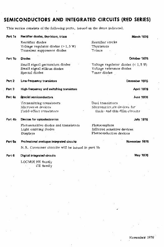
SEMICOND.UCTORS AND INTEGRATED CIRCUITS (RED SERIES)
This 'series consists of the following parts, issued on the dates indicated.
Part.. 1a Rectifier diodes, thyristors, triacs
Rectifier diodes Voltage regulatdr diodes (> 1, 5 W) Transient suppressor diodes
Part 1 b Diodes
Small signal germanium diodes Small signal silicon diodes Special diodes
Part 2 Low-frequency transistors
Part 3 High-frequency and switching transistors
. Part 4a Special semiconductors
Transmitting transistors l,,1icrowave devices Field -effect trans istors
Part 4b Devices for optoelectronics
Photosensitive diodes and transistors Light emitting diodes Displays
Part 5a Professional analogue integrated circuits
Rectifier stacks Thyristors Triacs
March 1976
October 1975
Voltage regulator diodes « 1,5 W) Voltage reference diodes Tuner diodes
December 1975
April 1976
June 1976
~Dual transistors Microminiature devices for
thick- and thin -film circuits
Photocouplers Infrared sensitive devices Photoconductive devices
July 1976
November 1976
N. B. Consumer circuits will be issued in part 5b
Part 6 Digital integrated circuits
LOCMOS HE family GZ family
May 1976
November 1976

COMPONENTS AND ,MATERIALS (GREEN SERIES)
This series consists of the following parts, issued on the dates indicated.
Part 1 Functional units, Inp~t/output devices, Peripheral devices
High noise immunity logic F Z /30-Series Circuit blocks 40-Series and CSA 70 Counter modules 50-Series NORbits 60-Series, 61-Series
Part 2a Resistors
Fixed resistors Variable resistors Voltage dependent resistors (VDR) Light dependent resistors (LDR)
Part 2b Capacitors
Part 3
Electrolytic and solid capacitors Paper capacitors and film capacitors,
Radio, Audio, Television
FM tuners Loudspeakers Television tuners and aerial input
assemblies
Part 4a Soft ferrites
F errites for radio, audio and television Beads and chokes
November 1975
Circuit blocks 90-Series Input/output devices Hybrid integrated circuits Peripheral devices
February 1976
Negative temperature coefficient thermistors (NTC)
Positive temperature coefficient thermistors (PTC)
Test switches
Ceramic capacitors Variable capacitors
April 1976
February 1975
Components for black and white television
Components for colour television
Octo,ber 1976
Ferroxcube potcores and square cores Ferroxcube transformer cores
Part 4b Piezoelectric ceramics, Permanent magnet materials May 1975
July 1975 Part 5 Ferrite core memory products
Part 6
Part 7
Ferroxcube memory cores Matrix planes and stacks
Electric motors and accessories
Small synchronous motors Stepper motors
Circuit blocks
Circuit blocks 100 kHz-Series Circuit blocks I-'Series Circuit blocks IO-Series
Part 8 Variable mains transformers
Part 9 Piezoelectric quartz devices
Part 10 Connectors
October 1976
Core memory systems
September 1975
Miniature direct current motors
September 1971
Circuit blocks for ferrite core memory drive
July 1975
March 1976
November 1975

General
Preface
Type designation
Package outlines
Ratings
Letter symbols


II II PREFACE
PREFACE TO DATA OF INTEGRATED CIRCUITS
1. General
The published data comprise particulars needed by designers of equipment in which integrated circuits are to be incorporated, and criteria on which to base acceptance testing of such circuits. For ease of reference, the data on each cir-· cuit are grouped according to the several headings discussed below. The limiting values quoted under the headings Characteristics and Package Outline may be taken as references for acceptance testing. Values cited as typical are given for information only. For an explanation of the type designation code, see the section Type Designation. For an explanation of the letter symbols used in designating terminals and performance of integrated circuits, and the electrical and logic quantities pertaining to them, see the section Letter Symbols.
2. Quick Reference Data
The main properties of the integrated circuit summarized for quick reference
3. Ratings
Ratings are limits beyond which the serviceability of the integrated circuit may be impaired. The ratings given here are in accordance with the Absolute Maximum System as defined in publication no. 134 of the International Electrical Commission; for further details· see item 2 of the section Rating Systems. If a circuit is used under the conditions set forth in the sections Characteristics and Additional System Design Data, its operation within the ratings is ensured.
4. Circuit diagram
Circuit diagrams and logic symbols are given to illustrate the circuit function. The diagrams show only.essential elements, parasitic elements due to the method of manufacture normally being omitted. The manufacturer reserves the right to make minor changes to improve rnanufacturability.
5. System Design Data and Additional System Design Data
System Design Data normally derived from the Characteristics and based on worst -case assumptions as to temperature, loading and supply voltage, are quoted for the guidance of equipment deSigners. Supplementary information derived from measurements on large production samples may be given under Additional System Design Data.
October 1968 II I] 1
-= ---

----
PREFACE II 6. Application information
Under this heading, practical circuit connections and the resulting performance are described. Care has been taken to ensure the accuracy and completeness of the infonnation given, but no liability therefor is assumed, nor. is licence under any patent implied.
7. Characteristics
Characteristics are measurable properties of the integrated circuit described. Under a specific set of test conditions compliance with limit values given under this heading establishes the specifie~ performance of the circuit; this can be used as a criterion for acceptance testing. Values cited as typical are given for information only and are not subject to any form of guarantee.
8. Logic symbols (digital circuits)
Graphical logic symbols accor¢l with MIL standard 806B. Supplementary drawings correlate logic functions with pin locations as a help to laying out printed circuit boards.
9. Outline drawing and pin 1 identification
Dimensional drawings indicC}te the pin numbering of circuit packages. Dual in-line packages have a notch at one end to identify pin 1. Take care not to mistake adventitious moulding marks for the pin 1 identification. Flat packs identify pin lby a small projection on the pin itself and/orby a dot. on the body of the package. Metal can encapsulations identify pin 1 by a tab on the rim of the can.
2 II II October 1968

II TYPE DESIGNATION
PRO ELECTRON TYPE DESIGNATION CODE
The type number consists of three letters followed by a four digit serial number (sometimes augm~nted by a version letter).
First two letters:
F amil y circuits
The first two letters identify the fa mil y.
Solitary circuits
The first letter identifies the circuit as:
S-digital T-analogue U - mixed analogue / digital
The second letter has no special significance.
The third letter indicates the operating ambient temperature range or another significant
characteristic. Letters B to F stand for the following temperature ranges: 1)
B: 0 to +70 °c c: -55 to +125 °c D: -25 to +70 °c E: -25 to +85 °c F: -40 to +85 °c
When no temperature range is specified, the third letter is A. Other third letters identify special family versions or treatments (e. g. radiation hardened).
The serial number following the three letters may be either a 4-digit number or a proprietary type designation comprising a combination of letters and digits. Proprietary type designations consisting of less than 4 characters are extended to 4 by putting zeros (0) before them~ __
1) If a circuit is published for a wider temperature range, but does not qualify for another classification, the letter deSignating the neares~tnarrower temperature range is used.
April 1973 II
--


----Package outlines


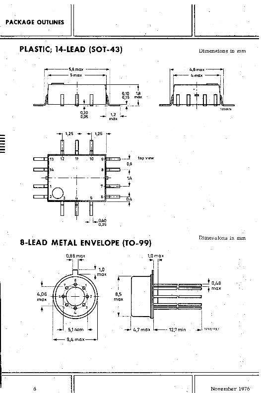
II PACKAGE OUTLINES
PLASTIC 8-LEAD DUAL IN-LINE (SOT -97) Dimensions in mm
~8.25max-QI C tI
il -. -3,4 2.9 +
~h2 max
+ 0,~5 I 3 min , - 076 BI
I 0,53 I + ' 6x 040 ~ '__ ~.lo;254@1 Al
__ i_i!:ii_i
SOLDERING
1,15 max
1. By hand
top view
I I
_II jt-0,26
I I
:1 II
. ~ 1'1 , ~
I 14---- 17,621 __ i I
9,5 7,6
.. 7Z73585
$ Positional accuracy.
@ Maximum Material Condition.
A) Centre -lines of all leads are within ±0,127 mm ofthenominaI position shown; in the worst case, the spacing between any two leads may deviate from nominal by ± 0,254 mm.
B) Lead spacing tolerances apply from seating plane to the line indicated.
Apply the soldering iron below the seating plane (or not more than 2 mm above it). If its temperature is below 300 °c it must not be in contact for more than 10 seconds; if between 300 °c and 400°C, for not more than 5 seconds.
2. By dip or wave
260°C is the maximum allowable temperature of the solder; it must not be in contact with the joint for more than 5 seconds. The total contact time of successive solder waves must not exceed 5 seconds. The device may be mounted up to the seating plane, but the temperature of the plastic body must not exceed the specified storage maximum. If the printed circuit board has been pre-heated, forced cooling may be necessary immediately after soldering to keep the temperature within the allowable limit.
3.. Repairing soldered joints
The same precautions and limits apply as in (1) above.
November 1976 II II
--

----
P~C:!(AGE OUTLINES .1
'PLASTIC 16-LEA,O OUAl"IN-LiNE
1 .... -------- 22 max
top view
SOLDERING
1. By hand
Dimensions in mm
I I I
II II II - III
.t~-~_r _9,5
7,6 -7ZS5041.6
$ Positional accuracy.
@ Maximum Material Condition.
A) Centre-lines of all leads are within ± 0, 127 mm of the nominal position shown; in the worst case, the spacin'g between any two leads rna y deviate f,rom nominal by ± 0,254 mm.
B) Lead spacing tolerances apply from seating plane to the line indicated.
Apply the soldering iron below the seating plane (or not more than 2 mm above it). If itstemperature is below 300 °c it must not be in contact for more than 10 seconds; if between 300 °c and 400 °c, for not more than 5 seconds.
2~ By dip or wave
260 °c is the maximum allowable temperature of the solder ;itmust not be in contact with ~he joint for more than 5 seconds. The total contact time of successive solder waves must not exceed 5 seconds. The device may be mounted up to the seating plane, but the temperature of the plastic body must not exceed the specified storage maximum. If the printed circuit board has been pre-heated, forced cooling maybe necessary immediately after soldering to keep the temperature within the allowable limit.
3. Repairing soldered joints
The same precautions and limits appl y as in (1) above.
2 II II Nov~mber 1976

II PACKAGE OUTLItiU
5.0-8 (SOT-96A); PLASTIC 8-LEAD FLAT PACK Dimensions in mm
I' ...... ~-- 5,Omax •
+ t 1,45 175 max max
... O,4Smax
r--'...J-r--,...J-r--. -' ,
,0,45 1' I
1 O,~ 11.-/.10,25 ®I .. 1,25 ..
top view
SOLDERING see last page of this chapter
November 1976 II
I' ...... ~-- 5,2max·--_.,
-~II- 4,Omax ~ I lli......!.'---:0~,1----Ttl 1
"'022 +min I 0:19 .. ~2max •
7ZS824D.2
$ Positional accuracy.
@ Maximum Material Condition.
3
-----

PACKAGE OUTLINES
II SO-lO; PLASTIC 10-LEAD FLAT PACK Dimensions in mm
I' ...... ~-- 5,2 max ----•• ,
1 __ ---- 6,25 max ----•• 1 .... ;;Pn -4,Omax_
• • ..... 0,45 max
--- 01
I ~ • min 0.22
0.19 .. . 6,2 max --7-Z-73-97-1 -t ... ,
-- r- r- r- r- r--
f- r- l"- f- l-
S 4 3 2 1 top view
$ Positional accuracy.
@ Maximum Material Condition.
6 7 8 9 10
l- I- l- t- t-l....- I....- l....- I..- ~
SOLDERING see last page of this chapter
II -November 1976

z o <: ('!)
~ ('!)
I-i f-' \0 -..J 0.
(JI
50-14; PLASTIC 14-LEAD FLAT PACK
14 835 max :1 • +
1,45 175 max ' , max
- t ,0,45/ ' I .... 035 \
0,45 max I '- 1-1+1 o.2s®1 .... 1,25 --
~ ~ ~ r-- r-- r-- r--
t- t- t- l- I-- l- I-
7 6 5 4 3 2 1 top view
8 9 10 11 12 13 14
t- l- I- l- I-- t- t-
'- ..... '-- l..- I..- l..- I..-
SOLDERING see last page of this chapter.
Dimensions in mm
• 5,2 max _I
.... 1 1,~ 1-+---4,Omax~ min
+ )...-J 0,1 ~-' -- •. min
1
0,2.2
0,19 6,2 max •
$ Positional accuracy.
@ Maximum Material Condition.
1111111
." ~ n ~ ~ o m
o c .... r-Z m CIt
--
PACKAGE OUTLINES
. PLASTIC; 14-LEAD (SOT -43)
1----5,6max --"'1
-- 1,25 ..
... 11 .. 0,40 0,25
max
t 1,8
max
•
top view
Dimensions in mm
~ 4,6 max------
8-LEAD METAL ENVELOPE (TO-99) Dimensions in mm
0,86 max
-'II~ 1,0
4,06 . max
i 8,5
max
1,0 max
-'1 1
-
• 1I~~5f§5'-:-- 0,48 II~ , + max
. t ' -::1 4,7ma, 1-12,7m;n _I "'''''.' -.1 5,1 nom _
-9,4max-
6 .11 November 1976

II PACKAGE OUTLINES
SOLDERING SO-PACKAGES
The Reflow Solder Technique
The preferred technique for mounting miniature components on hybrid thick or thin -film circuits is reflow soldering. Solder is applied .to the required areas on the substrate by dipping in a solder bath or, more usually, by screen printing a solder paste. Components are put in place and the solder is reflowed by heating. Solder pastes consist of very finely powdered solder and flux suspended in an organic liquid binder. They are available in various forms depending on the specification of the solder and the type of binder used. For hybrid circuit use, a tin-lead solder with 2 to 4% silver is recommended. The working temperature of this paste is about 220 to 230 oC when a mild flux is used. For printing the paste onto the substrate a stainless steel screen with a mesh of 80 to 105 Ilm is used for which the emulsion thickness should be about 50 Ilm. To ensure that sufficient solder paste is applied to the substrate, the screen aperture should be slightly larger than the corresponding contact area. The contact pins are positioned on the substrate, the slight adhesive force of the solder paste being sufficient to keep them in place. The supstrate is heated to the solder working temperature preferably by means of a controlled hot plate. The soldering process should be kept as short as possible: 10 to 15 seconds is sufficient to ensure good solder joints and evaporation of the binder fluid. After .soldering, the substrate must be cleaned of any remaining flux. .
November 1976 II II 7
----


II RATING SYSTEMS
RATING SYSTEMS
ACCORDING TO I.E.C. PUBLICATION 134
1. DEFINITIONS OF TERMS USED
1. 1 Electronic device. An electronic tube or valve, transistor or other semiconductor device. Note: This definition excludes inductors, capacitors, resistors and
similar components.
1.2 Characteristic .. A characteristic is an inherent and measurable property of a device. Such a property may be electrical, mechanical, thermal, hydraulic, electro -magneti<?, or nuclear, and can be expressed as a value for stated or recognized conditions. A characteristic may also be a set of related values, usually shown in graphical form.
1.3 Bogey electronic device. An electronic device whose characteristics have the published nominal values for the type. A bogey electronic device for any particular application can be obtained by considering only those characteristics which are directly related to the application.
1.4· Rating. A value which establishes either a limiting capability or a limiting condition for an electronic device. It is determined for specified values of environment and operation, and may be stated in any suitable terms. Note: Limiting conditions may be either maxima or minima.
1. 5 Rating system. The set of principles upon which ratings are estab - , lished and which deter:mine their interpretation. Note: The rating system indicates the division of responsibility be
tween· the device manufacturer and the circuit designer, with the object of ensuring that the working conditions do not exceed the ratings.
2. ABSOLUTE MAXIMUM RATING SYSTEM
Absolute maximum ratings are limiting values of operating and. environmental conditions applicable to any electronic device of a specified type as defined by its published data, which should not be exceeded under the worst probable conditions.
These values are chosen by the device manufacturer to provide acceptable serviceability of the device, taking no re sponsibility for equipment variations' environmental variations, and the eJfects of changes in operating conditions due to variations in the characteristics of the device under consideration and of all other electronIc devices in the equipment.
p.t.o.
January 1968 II II 1
----

--
i \
RATING SYSTEMS
II The equipment manufacturer should design so that, initially and throughout life, no absolute maximum value for the intended service is exceeded with any device under the worst probable operating conditions with respect to supply voltage variation, equipment component variation, equipment control adjustment, load variations, signal variatiGn, envh:onmental conditions, and variations in characteristics of the device under consideration and of all other electronic devices in the equipment.
3.' DESIGN MAXIMUM RATING SYSTEM
Design maximum ratings are limiting values of operating and environmental conditions applicable to a bogey electronic device of a specified type as defined by its published data, and should not be exceeded under the worst probable conditions.
These values are chosen by the device manufacturer to provide acceptable serviceability of the device, taking responsibility for the effects'of changes in operating conditions due to variations in the characteristics of the electronic device under consideration.
The equipment manufacturer should design so that, initially and throughout life, no design maximum value for the intended service is exceeded with a bogey device under the worst probable operating conditions with respect to supply voltage variation, equipment component variation, variationin characteristics of-all other devices in the equipment, equipment control adjustment, load variation, signal variation and environmental conditions.
4. DESIGN CENTRE RATING SYSTEM
Design centre ratings are limiting values of operating and environmental conditions applicable to a bogey electronic device of a specified type as defined by its published data, and should not be exceeded under normal conditions.
These values are chosen by the device manufacturer to provide acceptable serviceability of the device in average applications, taki,ng responsibility for normal changes in operating conditions due to rated supply voltage variation, equipment component variation, equipment control adjustment, load variation, signal variation, environmental conditions, and variations in the characteristics of all electronic devices.
,The equipment manufacturer should design so that, initially, no design centre vaiue for the intended service is exceeded with a bogey electronic device in equipment operating at the stated normal supply voltage.
NOTE
It is common use to apply the Absolute Maximum System in semiconductor published data.
2 II II January 1968

II LETTER SYMBOLS
LETTER SYMBOLS ' FOR LINEAR INTEGRATED CIRCUITS
General
The voltages and currents are normally related to the terminals to which they are applied or at which they ,appear. Each terminal is indicated by a number. In appropriate cases voltages, currents etc. pertinent to one or more of the circuit elements (transistors, diodes) are given in which case symbols are based on the recommendations as published in 1. E. C. Publication 148.
Quantity symbols
1. Instantaneous values of current, voltage and power, which vary with time are represented by the appropriate lower case letter.
Examples: i, v, P
2. Maximum (peak), average, d.c. and root-mean-square values are represented by the appropriate upper case letter.
Examples:' I, V, P
Polarity of current and voltage
A current is defined to be positive when its conventional direction of flow is into the device. A voltage is measured with respect to the reference terminal, which is indicated by the subscripts. Its polarity is defined to be positive when the potential is higher than that of the reference terminal.
Subscripts
For currents the number behind the quantity symbol indicates the terminal carrying the current.
Examples: 12, i 14
For voltages normally two number subscripts are used, connected by a hyphen.The first number indicates the terminal at which the voltage is measured and the second subscript the reference terminal. Where there is no possibility of confusion the second subscript may be omitted.
Examples: V2-l2, v14-2, V5, v8
November 1971 II II 1
---.. ...

--
LETTER SYMBOLS
II To distinguish between maximum (peak), average,d.c.androot-mean-square values the following subscripts are added:
For maximum (peak) values : For average values For root-mean-square values: For d.c. values
Morm AV or av (RMS) or (rms) no additional subscripts
The upper case subscripts indicate total values. The lower case subscripts indicate values of varying components:
Examples: 12, 12AV, 12(rms), 12(RMS)
If in appropriate cases quantity symbols are pertinent to single elements ofa circuit (transistors or diodes), the normal subscripts for semiconductor devices can be used.
Examples: VCBO, Vbe, VCES, IC
VOSS,' VGS, 10
List of subscripts:
E, e B, b
C, c 0, d G, g S, s
(BR) M,m AV, av (RMS) , (rms) =
Emitter terminal Base terminal for bipolar transistors, Substrate for MOS devices
, Collector terminal Drain terminal Gate terminal Source terminal for MOS devices Substrate for bipolar transistor circuits Break-down Maximum (peak) value Average value R.M.S. value
Electrical Parameter Symbols
1. The values of four pole matrix parameters or other resistances, impedances, admittances, etc., inherent in the device, are represented by the lower case symbol with appropriate subscript.
Examples: hi, zf, Yo' kr
Subscripts for Parameter Symbols
1. The static values of parameters are indicated by upper case subscripts.
Examples: hFE' hI
2. The small signal values of parameters are indicated by lower case subscripts.
Examples: hi' Zo
2 II II November 1971

II LETTER SYMBOLS
3. The first subscript, in matrix notation identifies the element of the four pole matrix.
i (for 11) = o (for 22) = f (for 21) = r (for 12) =
input output forward transfer reverse transfer
Examples: VI = hi II + hr V 2
12 = hfl l + ho V 2
The voltage and current symbols in matrix notation are indiCated by a single digit subscript. The subscript 1 = input; the subscript 2 = output. The voltages and currents in these equations may be complex quantities.
4. A second subscript is used only for separate circuit elements (e.g. transistors) to identify the circuit configuration:
e = common emitter b = common base c = common collector
5. If it is necessary to distingui.sh between real and imaginary parts of the four pole parameters, the following notation may be used:
Re (hi) etc. for the real part 1m (hi) etc .... for the imaginary part
November 1971 II 3
--

----
LETTER SYMBOLS
II
"_LIST OF LETTER SYMBOLS IN ALPHABETICAL ORDER
Letter symbol \
B
CMMR
d
P
f
" fc
fo
fm
Gp
Gtr
Gv
hp, hFB. hpC' hPE
hf ,hfb. hfc ' hfe
13. lB. IC, IE. ID, IQ' IS
i3' iB• iC' iE~ iD' iG'" is
13AV, IBAV. ICAV, IEAV
13M' IBM' ICM. IEM
13m' Ibm' Icm ' Iem
ICBO
ICS
IDSS
4 II
Definition
Bandwidth
Input, respectively output susceptance
Input, respectively output capacitance
Common -mode rejection "ratio
Distortion
Noise f~gure
Frequency
Cut-off frequency
Centre frequency, intermediate frequency
Modulation frequency
Transition frequency
Input,respectively output conductance
Power gain
Transducer gain
Voltage gain
DC current gain (output voltage held constant)
Small signal current gain (output short-circuited to a.c.)
Total d. c. current
Instantaneous total value of the current
Total average current
Maximum (peak) value of the total current
Maximum (peak) value of the varying component of the. current '
Collector cut -off current (open emitter)
Collector-substrate leakage current
Drain cut-off current (source short-circuited to gate)
I November 1971

Letter symbol
lEBO
II' Ii
Iio
10 , 10
10M
Io(p_p)
l tat
Kf
Ko
Kr
M
RL
RS
Rth
SVRR
Tamb
Tcase
T stg
II
V3' V3-4, VBE, VCB
v3' v3-4, vBE' vCB
V BEsat' V CEsat
V (BR)CBO' V (BR)CEO'
V(BR)EBO
V(BR)CS
VCBO ' VCEO ' VEBO ' VCS'
V 1-3
November 1971
LETTER SYMBOLS
Definition
Emitter cut-off current
Input current of a specified circuit
Input offset current
Output current of a specified circuit
Peak value of output current
Peak to peak value of output current
Total supply current
Small signal voltage gain
Output impedance (see K parameters)
Reverse current transfer ratio
Modulation depth
Input, respectively output power of a specified circuit
Total power dissipation in the device
Input, respectively output resistance of a specified circuit
Load resistance
Source resistance
Thermal resistance
Supply voltage rejection ratio
Ambient temperature'
Case temperature
Storage temperature
Total value of the voltage (d.c.)
Instantaneous value of the total voltage
Saturation voltage at specified bottoming conditions
Breakdown voltage between the terminal of the first subscript and the'reference terminal (second subscript) when the third terminal is open circuited
Collector to substrate breakdown voltage
Voltage of the terminal indicated with respect to the reference te,rminal (second subscript)
II 5
-------

-LETT'ER SYMBOLS
Letter symbol
Vi,Vo
V· . 10
Vi lim
VN
Vp
Vn
Yi' Yf· Yo' Yr
Zi. Zo --- n -- cP i' cP f' cp 0 ,Cf> r
6
II
II Definition
Input, respectively output voltage of a specified circuit
Input offset voltage
Input voltage at which limiting starts
Negative supply voltage
Positive supply voltage
Noise voltage
Input, transfer, output and feedback admittance
Input, respectively output impedance
Efficiency
Phase angle of input. transfer. output and feedback admittance
November, 1971

AMPLIFIERS

TYPE SELECTION l II Amplifiers
TBA221D - op ,amp
TCA220 - triple op amp
TCA41OA; B; D - voltage follower
TCA520B; D - op amp
TCA680; B; 0 - high slew rate op amp
TD.A0301D - op amp
TDA0324D - quadruple op amp
TDA0358D - dual op amp
TDA0741D - general' purpose op amp
TDA0748D - general purpose op amp
TDA1034; B; D - low noise op amp w
:! TDA1458D - dual op amp ... TDA4250B; D - programmable op amp ...
..Iiiio
II II November 1976

II II TBA221D
OPERATIONAL AMPLIFIER
The TBA221D is a silicon monolithic integrated operational amplifier for use at temperatures from -25 to +85 °C. Special features are:
- no frequency compensation required - 'continuous short-circuit protection - offset voltage adjustable to zero - large input voltage range - low power consumption - no latch up
TBA221D is equivalent to IlA741C, but has better specifiedd.c. parameters and lower noise.
Positive supply voltage
Negative supply voltage
QUICK REFERENCE DATA
Characteristics at T amb = 25 OC
Voltage gain at RL = 2 kQ; Vo = flO V
Common mode rejection ratio
Differential input resistance
Output voltage swing at R L= 10 kQ
Input voltage range
Gv
CMRR
Ri
Vo
Vi
typo
typo
typo
>
>
15 V
15 V
200000
90 dB
2 MQ
±I2 V
±12 V
PACKAGE OUTLINE 80-8 (SOT-96A) (plastic 8-lead flat pack) (see general section).
June 1976 II II

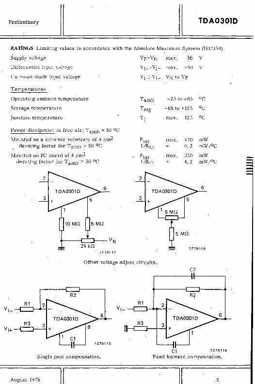
II RATINGS Limiting values in accordance with the Absolute Maximum System (IEC 134)
Voltages
Positive supply voltage
Negative supply voltage
Common mode input vOltage 1)
Differential input voltage
Pciwer dissipation (see derating curve below)
Total power dissipation (free air, T amb = 50 OC) mounted on a ceramic substrate (4 cm2)
mounted on printed;circuit board (4 cm2)
Output short-circuit duration 2)
= Temperatures
Operating ambient temperature see derating curve below
Storage temperature
500
Ptot (I'nW)
250
o o
" " I'(
~
I'ooL
"
50
L , I
I L 11 I J J
Tamb
Tstg
1Z13919
11111111 LI 11 J LJ LI J J on ceramic substrate-t-t-t-
I
L IIL.I I 1 J J r r /I I I II I JJLl L1J
"' "" on printed-circuit board
"-
"" '" I'
" " " ~ ~
max.
max.
max.
max.
max.
max.
20 V
20 V
±15 V
±30 V
470 mW
310 mW
indefinite
-25 to +85 °C
-65 to +150 °C
1) For supply voltages less -than ±15 V, the absolute maximum'input voltage is equal to the supply voltage.
2) Continuous short circuit is allowed to ground or either supply.
2 II II June 1976

II II TBA221D
CIRCUIT DIAGRAM
2
6 ----R" --SOil
5
November 1974 II 3
TBA221D
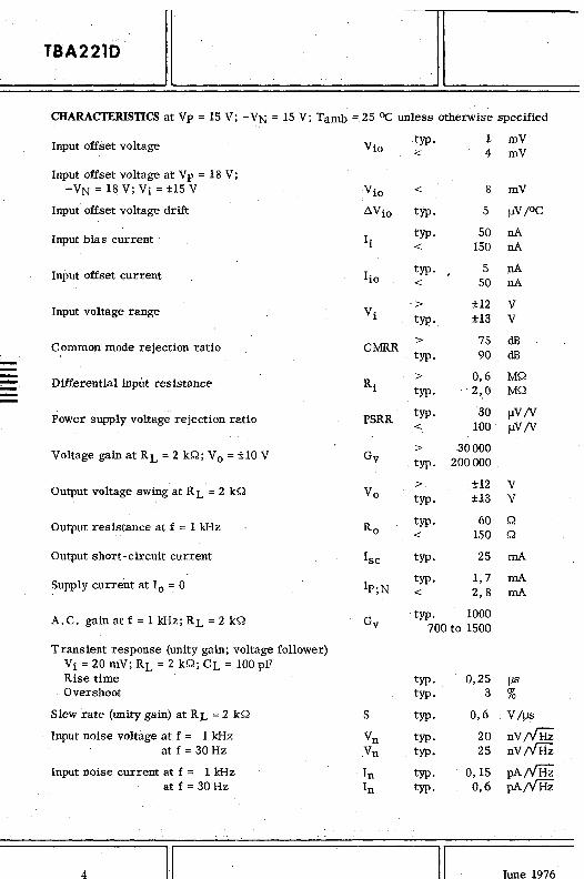
II II CHARACTERISTICS at Vp :::: 15 V; -VN :::: 15 V; Tarnb :::: 250C unless otherwise specified
Input offset voltage Vio typo 1 mV < 4 mV
Input offset voltage at V P :::: 18 V; -VN :::: 18 V; Vi :::: ±15 V Vio < 8 mV
Input offset voltage drift ~Vio typo 5 flV 1°C
Input blas current Ii typo 50 nA < 150 nA
Input offset current Iio typo
i 5 nA
< 50 nA
.> ±12 V Input voltage range Vi typo ±13 V
> 75 dB C,ommon mode rejection ratio C~R typo 90 dB .....
0,6 MQ - > - Differential input resistance Ri - typo 2~O MQ
Power supply voltage rejection ratio PSRR typo 30 flV IV < 100 flV IV > 30000
Voltage gain at RL :::: 2 kQ; Vo :::: ±10 V Gv typo 200000
> ±12 V Output voltage swing at R L :::: 2 kQ Vo typo ±I3 V
Output resistance at f :::: 1 kHz Ro typo 60 Q < 150 Q
Output short-circuit current lsc typo 25 rnA
?upply current at 10 :::: 0 Ip;N typo 1,7 rnA < 2,8 rnA
A.C. gain at f:::: 1 kHz; RL = 2 kQ Gv typo 1000
700 to ·1500
Transient response (unity gain; voltage follower) Vi :::: 20 mY; RL :::: 2 kQ; CL :::: 100 pF Rise time typo 0,25 J.lS Overshoot typo 3 %
Slew rate (unity gain) at RL :::: 2 kQ S typo 0,6 . V IflS Input noise voltage at f :::: 1 kHz Vn typo 20 nV!"fH.;,
at f:::: 30 Hz Yn typo 25 nVtfHZ
Input noise current at f :::: 1 kHz In typo 0,15 pArVHZ at f:::: 30 Hz In typo 0,6 pA;VHZ
4 II II Tune 1976

II II TBA221D
CHARACTERISTICS at Vp = 15 V; -VN = 15 V; Tamb = -25 to +85 OC unless otherwise specified
Voltage gain at RL = 2 kQ; Vo = ±10 V
Input offset voltage
Input bias current
Input offset current
. Output voltage swing at R L = 2 kQ
+
Vp
7
TBA221 6
7ZSSS90
Offset voltage zeroing circuit
Vp
. Transient response test circuit
June 1976 II
Gv > 20000
Vio < 5,5 mV
Ii < 0,3 !.lA Iio < 0,1 !.lA Vo > 11,5 V
II 5
--

-----
lBA221D II
7Z69312
200 Vp=VN=15V t-r-
100
o
35
Isc (rnA)
30
25
-/20
15
~ ~
.....
I
o
r- -
I-... i"""" I'-.
o
6
r-.... , ',typ
J"".r-., ,
I
. I
i f---r-i-
25
--j-
,
I I
............... I l' typ
........
I I
2S
II
......... r--., ...... r---~
,
j--f--
7269311
j: +-j
"
i I
I
:
I
r- ~-
~
i"""" ~ ; ........ I'-.
1
I i 50 75'
Tomb (OC)
10
5
4
3
lIV
lIV
:;
2
'Ill
1 o
125
Gv (dBI
100
75
50
--
lJ1' I'
i/ ,
,
, 1
)
o
"-
Vll
JI'
7Z70182
Vp =VN=15V
~)I
)1 ~yp
1
7Z693'S
j _L J1 J.J.l Tamb = 25°C t-ct-
I -,±--.... - 'I , + ~+-"""'typ I
J -t-"-
I
'1 r _L )
10 20
November 1974

30
I io
(nA)
20
10
'-I---
..........
" i I
1-1-'-, -+
1-1- -'-I-1--1- --I- 1-1-----
60
Va (p-p)
(V)
40
20
I
!
1
November 1974
I
I 1-+-I
IT
I 1
-+-1
i +-~
~
1/
7Z69310
1 1 I 1 .111111 Tamb =25°C 1-1-
typ I"""
1
I
I
I I r-
I I 1 i
10 20
7Z69308
I 1 I I 1 1 Tamb=O to 70°C 1-1-
RL=2kfl I-t--
1 1 I I
!
I' :/
I 1/ / ~---
typ
!
I 10 20
40
1'0 (nA)
30
20
10
o
15
10
5
II TBA221D
7Z69313 ,
Vp =VN =15V t-I--
\ ~
\ I
~ I
I' I
~ I, _,
I,typ
I " I
I I ~ .1 I "'}...
! I r-I
I j [
f
----I 1
o 25 50 75
7Z69314
I ! I I i I I I I I
r-r- Tamb=O to 70°C '[ ,I
IL
IL
L -' I
.L typ 'I
--'-J
I -+- -
I J I
r-i -' I I 1-1-
--'-r-~ ~- -
J I
"- I
I J. 1 I 1 I
1J J. J.J. i i 1 ' i I '
10 20
II 7
------
TBA221D II 150
Ptot (mW)
100
50
10
1
7Z69307
I I I I Tomb=25°C f-f-
J :1
~ If
J
ty~} f-f-r-
~
V V
V V
V ~
~
I;"
7Z69316
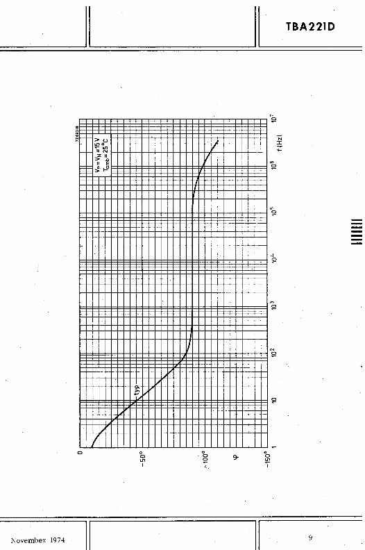
Vp =VN =1SV
~ Tamb =2SoC
1\ 1\ ~
I 1\ 1\
~ 10 102 103 104 105 106 107
f{Hz)
8 II
30
Vo (V)
20
J
1 II
iLil
II typ
I V
10
/
25
Vo (mV)
20
15
10
5
o
-5
1-'-
I-r-
-1
IT ~
f--900;0
10% tr
o
II 7Z69309
~ :.-1-1-'''
~
~
Vp=VN=15V
TOmb=25°C
10
7255584
Vp; - VN=15V I-r-Tomb = 2SoC r-r-
r-r-RL=2kn. t-f-CL =100pF r-r--.l -.l-.l-.l
I I I I 2 3
t(f.lS )
II November 1974
II
.,
... f->u Nf-
.... f- f- Lll 0 ..... Lll
f->.- II N Z II
> .0 II E :=:= == ~t-5'
'/
I a
November 1974
0. ~I' >.
+'~
o a Lll I
I
V
/
/
o , a ~ l,
V
9-
II
II
N
o a Lll
'I
~
N I ....
TBA221D
9

--
TBA221D
30
Vo (p-p)
(V)
20
10
100
CMRR . (dB)
75
50
25
o 1
iO
II
I
..........
10
\ , ,. , , \ \ \ typ \ \ \ l r\.
\ \
10 4
i'... ',,-
ro...
II . 7Z69317
I I II I liT
Vp=VN=1SV Tamb= 25°C R.L=10kO
~
I"\,
'" ,
.......... ..... f(Hz)
7Z70184
III I Vp =VN =15V Tamb= 25°C C =30pF
~P
'~ .....
........
" ro..."
November 1974

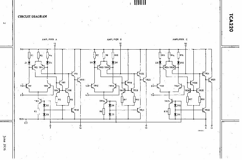
II II TCA220
TRIPLE OPERATIONAL AMPLIFIER
The TCA220 is a monolithic integrated circuit, consisting of three identical highgain amplifiers. The amplifier:s have a differential input stage and an emitter-follower output stage, which can supply a current up to 100 rnA. The unity-gain frequency with 6 dB/octave compensation is 5 MHz minimum. No latch -up occurs if the input voltage range is exceeded.
QUICK REFERENCE DATA
Positive supply voltage
Negative supply voltage
Voltage gain
Common mode rejection ratio
Supply voltage rejection ratio
Input offset voltage
Input offset current
Gv
CMRR
SVRR
Vio
lio
nom.
nom.
typo
typo
typo
typo
typo
6
6
4000
90
200
2
0,2
PACKAGE OUTLINE plastic 16-lead dual in-line (see general section).
August 1976 II II
v V
dB
jJV/V
mV
jJA
N
'a' ~ ..... \0 -..J Q\
CIRCUIT DIAGRAM
160 ,
AMPLIFIER A
15
14
D5
AMPLIFIER B
12
+ 40~-----+------~
II 11111
TR22
13
AMPLIFIER C
10
11
.... n » ~ ~ o
II TCA220
RATINGS Limiting values in accordance with the Absolute Maximum System (IECI34)
Voltages
Supply voltage
Common mode input voltage
Differential input voltages
Pin No. 9 voltage
Currents
Input currents (pins, I, 2, 4, 5, 7, 8)
Output currents (pins 14,
Bias current (pin 3)
Total power dissipation
750
Ptot (mW )
500
250
o -100
Temperatures
Storage temperature
Junction temperature
l3, 11)
-50
V6-l6
Vi
±Vl-2
} ±V5-4 ±VS-7
V9- 16
11;12 } 14; 15 17; 18
-I14;-I13;-Ill
13
, , I'
o
max. 18
max. 18
max. 5,0
max. a
max. a,s
max. 100
max. 5,0
7Z623221
~ -t-1-
\. , " ~
i\.
-55 to +125
max. 125
V
VI)
V
v2)
rnA
rnA
rnA
°C
°c
1) For a total supply voltage less than 18 V, the absolute maximum input voltage is equal to the supply voltage.
2) If amplifier C is used, pin 9 must be connected to pin 16.
April 1973 II II 3
----

== ----
i TCA220
II 11 THERMAL RESISTANCE
From junction to ambient max. 160
CHARACTERISTICS (each amplifier) at V P = 6 V;-VN = 6 V; T amb = 25 0 C RL = 10 kQ (unless otherwise specified)
Voltage gain at ± YOM = 3,5V Gv typo 4000 2
Input offset voltage at RS.$ 200 Q
Input bias current
Input offset current
Common mode rejection ratio at RS =2 kQ . CMRR
Input voltage range Vi
Differential input resistance Ri
Supply VOltage rejection ratio at RS = 2 kQ SVRR
Peak output voltage swing YOM
Total current at Vo = 0; RL = 10 kQ Itot at V 0 = 0; R L = ~ Itot
Slew rate (unity-gain)
Blas current (all three amplifiers together) 13
Channel separation between amplifiers A and B between amplifiers A and C between amplifiers Band C
Frequency compensation circuit Vp , 6
TCA220 14 2 + (ampl. A)
~ 330pF
{ t~. 10
{ t~. 1,0 2,0
typo . 0,2
typo 90
-4,3 to +5,6
> 25
typo 200
-6 to +3,5
typo 1,0 typo 0,4
typ~ 0,4
> 200,
typo 94 typo 130 typo 110
°C/W
mV mV IlA IlA
IlA
dB
V
-kQ
IlV/V
V
rnA rnA
V/Ill:!
IlAl)
dB2) dB2) dB2)
1) The voltage at pin 3 is always 2 diode voltages (approx. 1,5 V) above the negative supply voltage; if the bias current in obtained from the positive supply voltage a dropping resistor Rp.$ Vp - VN - 1,5
200.10 6. gives minimum power consumption. V
oA 2) Channel separation defined as 20 log V- x GB, if GB is the closed loop gain of
amplifier B. oB
4 II April 1973

II
VOLTAGE FOLLOWER
TCA410A; TCA410B TCA410D
The TCA410 is a silicon monolithic integrated operational amplifier internally connected as a voltage follower. -Special features are:
- very low input current;
- continuous short-circuit protection;
- no frequency compensation required
- small package (TO-72 or SOT-95A)
For most applications the TCA410 can be usedas a direct replacement for the LM302 and LM31O. The TCA410D is pin to pin'compatible with the TBA221D, whenthe latter is connected as a voltage follower.
QUICK REFERENCE DATA t----.c--.----------------------------------l
Supply voltage range Vp= -VN
Input bias current Ii
Input offset voltage V io
Output short-circuit current Isc
Output voltage swing at RL = 5 kQ Vo
Slew rate S
PACKAGE OUTLINE (for TCA410D see page 2)
TCA410A; TCA41OB: TO-72
2
TCA410A TCA410D
typo 0,5
max F=====~====~ F=====::::O
typo
typo
typo
typo
4~8 D· ~ - I
1 __ 5,3 ... 1_ 127min _ 7166167 max '
pin 4 connected to case
June 1976 II
5 to 18 V
TCA 4 lOB
1,5 nA
3 mV
10 rnA
13,5 V
4 V/flS
Dimensions in mm
1 = Vo 2 = Vp 3 = Vi 4=VN
----
-----
TCA410A; TCA410B TCA4100
PACKAGE OUTLINE (continued)
TCA410D; SOT-95A (plastic 6-1ead flat pack)
... 0,45 max
ro- r--
~ ~
3 2
4 5
~ ~
'-- l...-
1. Nat connected 2. Input 01 i) 3. Negative supply (VN) 4; Nat connected 5. Output (V 0) 6. Positive supply (Vp)
2
+
r--
~
1 top view
6
f-
I...-
Dimensions in mm
14 5,2 max .-
.... 1,0 -4,O·max ______ I min
1.1_+ 01
I ~ + min 0,22 0,19 ... 6,2 max -:--;----..,
, II June 1976

II CIRCUIT DIAGRAM
TCA410Ai TCA410B JCA410D
r---~--~--------~------------~--~--~~--------~--oVp
R15
R16
R13
.-------~------~~--------~----------+------------+--OVN 1Z67179.2
June 1976 II 3

-.. -
TCA410Aj JCA410B TCA410D \. . [I RATINGS Limiting values in accordance with the Absolute Maximum System (lEe 134)
Voltages
Positive supply voltage
Negative supply voltage
e ammon mode input voltage
Differential input/output voltage
Power dissipation (see derating curve)
Temperatures
Operating ambient temperature
Storage temperature metal envelope; TO-72 plast,ic flat pack; SOT-95A
4
400
Ptot (mW )
200
I
" "'"
50
, I),;
'" it'" l' I(' , .... "
"-~
Tamb
T stg T stg
7Z72806
max. 18 V
max. 18 V
VN to Vp
max. ±6 V
max. 250 mW
-25 to +85 °e
-65 to +125 oe -65 to +125 °e
T07"72 with he'atsink V 0
I I' .100 C/W
SOT-gSA
~:rO-72
I' I" I\.
f"-1"-~l"-!~
I'~l\. ~
"
II June 1976,

II TCA410A; TCA410B
TCA410D
CHARACTERISTICS at Vp = 15 V; -VN = 15 V; Tamb = 25 oC
TCA410A B D
Input bias current Ii typo 0,5 1,5 0,5 nA < 1, ° 3,0 3,0 nA
Input offset voltage Vio typo 3 mV < 10 mV
Input offset voltage drift I:::.Vio typo 20 IlV 1°C
Voltage gain at RL = 5 kQ; Vi = ±12, 5 V > 0,9980
Gv typo 0,9995
> ±12,5 V Output voltage swing at RL = 5 kQ Vo typo ±13,5 V
Output resistance at 10 = ±6 rnA Ro typo 0, 7 Q
< 2,0 Q
typo 10 rnA -Output short-circuit current Isc -
6 to 14 rnA
:> 2,5 V IllS Slew rate S typo 4,0 V IllS
Supply current Ip; N typo 2 rnA < 3 rnA
> 65 dB Power supply voltage rejection ratio PSRR
typo 75 dB
Supply voltage range VP.= -VN 5 to 18 V
Input capacitance Ci typo 2,5 pF
Input noise voltage at f = 1 kHz Vn typo 80 nV;v'Hz at f = 10 Hz Vn typo 200 nV;v'Hz
Input noise current at f = 1 kHz : TCA410A In typo 0,006 pAj'I/H;, TCA410B In typo 0,015 pA;v'Hz
at f = 10 Hz : TCA41QA In typo 0,04 pAj'I(H;. TCA410B In typo 0,1 pAt/HZ
June 1976 II 5

---
TCA410Ai TCA410B TCA410D
3
2
'1
l'\..
~
, ~
'" .... ~ 1" ......
II 7Z67471
Vp=15V -VN=15V
typo values
TCA410B I"i"oo., ...... r....
r- ..... ~ - r-
r-~ ~ TCA410A;D
10
Pv (dB)
o
-10
-20
6
o -25
-I-~
~ ~
, \ \
!\ , \ I,
I
~
RS=100kQ I I
I I I
o
-I"-r-t-I-..L. J. .,. ,
I !-
25
1Z67472
II Vp=15V
-VN=15V RL=5kQ
Rs~ol-A
/
~. \\ \ I\CL=O \ , ,
~
1\ CL= 1100pF
. --.- \ III1I1 ~ II II
107 f (Hz) 108
II
Vp
TCA410
4
June 1976

1-10-4
(0,9999)
1-10-3
(0,999)
1-10-2
(0,99)
1-10-1
( 0,91102
10
Vnlrms) -(IJV/IRZ)
10 Hz
10-1 1 kHz
II 7Z72810
Vp =15V -VN =15V
typ
~
~ "'
103 10
4 f (Hz) 10
5
10-2~-----r-----1------+-----~
10-3
104 105 106 107 108
Rs (.fl.)
June 1976 II
3
)
2
o o
20
Isc (rnA)
15
I'
~ 10
5
0
I"
'"
typ ...... 1/
II"
TCA410A; TCA410B TCA410D
7Z72807
, I"
1/ ';r
10 Vp; -VN (V) 20
7Z72809
Vp = -VN =15V
~
'" ~ -25 0 25 50 75 100
Tamb ,(oCI
7
=


II
OPERATIONAL AMPLIFIER
TCA520B TCA520D
The TCA520 is a silicon monolithic integrated cir~uit primarily intended for use in low power, low voltage applications and as comparator in digital systems. Special features are:
- large supply voltage range : 2 to 20 V - offset voltage adjustable to zero - output TTL-compatible - low power consumption - high slew rate (comparator) - low input bias current
Supply voltage
Output sink current
Input current
Slew rate (comparator)
: 5 mWat 5 V : 50 V /jJS : 30 nA
QUICK REFERENCE DATA
PACKAGE OUTLINES (see general section).
TCA520B : SOT-97 (plastic 8-lead dual in-line). TCA520D: SOT-96A (plastic 8-1ead flat pack).
June 1976 II
Vp nom.
Isink typo
Ii typo
S typo
"
5 V
12 rnA
30 nA
50 V/fis
1

TCA52()B TCA520D
CIRCUIT DIAGRAM
II
----~~------~----~------~----------o7
5O-----4-4--4-+---------r--~
2o---------~----~ 6
7Z67240
CONNECTION DIAGRAM AND PINNING
C 1. Balance
2. Inverting input
3. Non-inverting input
TCAS20B;O ~6~ ...... -o output '4. Negative supply (VN)
5. Frequency compensation
6. Output
7. Positive supply (V p)
8. Balance
Sk.Cl. 7Z67241.1
2 II "
June 1976

II TCA520B TCA520D
RATINGS Limiting values in accordance with the Absolute Maximum System (lEC 134)
Voltages
Positive supply voltage
Negative supply voltage
Different~al input voltage
Temperatures
Operating ambient temperature
Storage temperature
Maximum power dissipation in free air
package mounting max. power dissipation
at Tamb = 50 oC (mW)
SOT-97 on PC board 375
SOT-96A on· ceramic substrate (4 cm2) 440
SOT-96A on PC board (4 cm2) 300
June 1976 II
Vp max. 11 V
-VN max. 11 V
±V2-3 max. 6 V
Tamb -25 to +85 oC
T stg -65 to +125 oC
derating thermal factor for resistance
Tamb> 50 °C Rth j-a (mW JOC) (OCjW)
5 200
5,8. 170
4 250
II 3

lCA520B TCA520D
CHARACTERISTICS Vp = 5 V; VN = O'V; Tamb ="25 oC; RL connected between output (pin 6) and positive supply (pin 7)
Vio typo 1 mV
Input offset voltage < 6 mV
Input offset voltage drift . ~Vio typo 5 IlV/oC
Ii typo 30 nA
Input bias current < 100 nA
Iio typo 5 nA
Input offset current < 30 nA
> VN + 0,9 V Input voltage range Vi > Vp - 0,5 V
CMRR > 70 dB Common mode rejection ratio typo 100 dB
> 25 000 D. C. voltage gain at RL =: 5 kQ Gv typo 50000
A. C. voltage gain at f =: 1 kHz; C ;::: 100 pF Gv 600 to 1800 - 1000 typo
> VN + 0,1 V Output voltage range at R L =: 5 kQ Vo > Vp - 0,1 V
Output sink current at Vo ;::: VN + 0,4 V > 8 rnA
Isink typo 12 rnA
Output source current at V 0 $ Vp - 0,4 V > 0,13 rnA
Isource typo 0,20 rnA
typo 1 rnA Supply current at 10 ;::: ° Ip;N < 1,5 rnA
Slew rate at C = 100 pF; RL = 1 kQ S typo 0,3 V IllS atC =O;RL = 1 kQ S typo 50 V IllS
Input noise voltage at f = 1 kHz Vn typo 15 nV ('/H;,
Input noise current at f = 1 kHz In typo 0,2 pAj'/Ti;,
4 II June 1976
- ......
""" """",--
-- "' 1\
r~-
r-
---l-I i I
10 .-
--I
I
I
June 1976
II
..........
~
"' "
, I'
; " C = 100pF
-'"
i I ! I - . r-
~-
I
I I
TCA520B TCA520D
1Z672 42.1
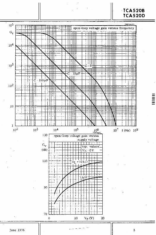
open :"loop voltage gain versus frequency
~ C 0
C =lOpF
" r\
'" , ,
" "- 1\ 1'1 I
! ~
, , "\. ,
\ 107 f (Hz) 108
130 open-loop voltage gain versus supply voltage
I I I I I I I typo values l-I 1 VN=OV ~
r~ r.-- I I I I
110 RL=lO~~ '---I~
....,.. I I ~ I I
! i ..... I I
I" 1kQ 1/ 10-1-1"'"' / i-o"
I .... 1"""
90 1/ ~
J I" I II"
V 1/
I
70 o 10 Vp (V) 20
II ---_.--------- .
5
=

--
TCA520B TCA520D
10
C =0; S = SOV IllS
C = 1 pF; S = 25 V IllS
C = 10 pF ; S = 3 V III s
C = 100 pF; S = 0,3V I~s ...... 100-
\. \ , , \.
" \.
" " \.
II 7Z67441
t\
~
\
1\
\ 107 f (Hz) 108
Frequency response and slew-rate for various closed-loop gains
6 II June 1976

60
40
20
o
0,75
Isource (rnA)
0,5
0,25
o
II 7Z67444
input bias current versus supply voltage
I I I I I i f- typo values I i ii
I- VN=OV t-t- ~~~~=1_120 bd= ,",,1-"'1"'"
'" ~
~25 t-t-If' 1/ t-t-
.... 10-~7~ t-t-1/ I .....
t=t:: ~ 1/ ...
J ..... 1"'" I " 1/ J
I
o 10 Vp (V) 20
7Z67442
output source current I' I I I versus output voltage typo values t-
I"-I-!o.. VN=OV t-r-,....i"-o
r-t-+-Vp=20V r-~
--~I-o 10 r-
f-f- 1-5 ~ ...
!"'I
2. I I
o 10 Vo (V) 20
June 1976 II
60
Isink ,(rnA)
40
20
o
30
VO(P-p)
(V)
20
10
o
o o
lCA520B TCA520D
7Z67443
output sink current versus output voltage
i ~ i typo values t-VN=OV t-
Vp=20V
'tI"
I 10 ..... J
--5 I
~2
10 Vo (V) 20
7Z67445
peak-to-peak output voltage versus supply voltage
i~ ~
RL=lkQt-
It"" 1/
It"" Ii"
V min , 'L
I'
II" II"
If' If'
10 Vp (V) 20
II 7
---

--
lCA520B TtA52PD
100
Vi (mV)
0
-100
5
Vo (V)
2,5
o
II r-----1~------__..-<> + 5V
7 2
TCA520B;O
3 +
~ ---,...-_ .. I I I I I I I L
I I
I I ~ __ ...J
.1
,1 I I
I , \.1.
o 2
5 1 k.C'l.
... 6_ ..... _0
output (Vo )
7267447.1
i I I I I 1
7Z67448
_ .... _--
4 5 time (fJs)
The TCA520B;D used as a comparator; pulse delays when the circuit is 20 or 100 mV overdriven. .
II II June 1976

V~(rms) (nV/fflz )
~ 10
1 10
June 1976
II 7Z72804
typ
103
f (Hz) 104
II
102
I n(rms)
(pAiIHi )
10
~
10-2
10
~ ~typ
102
II
TCA520B TCA520D
1Z72805
103
f (Hz) 104
9


II
OPERATIONAL AMPLIFIER
TCA680; TCA680B TCA680D
The TCA680 is a silicon monolithic integrated operational amplifier intended for general purposes, havmg a considerably improved slew rate and bandwidth compared to the TBA221 (f1A741C). Special features are:
- internal frequency compensation; - output short-circuit protection; - pin compatible with general purpose operational amplifiers; - offset voltage adjustable to zero.'
QUICK REFERENCE DATA 1----
Slew rate
Unity gain frequency
Input bias current
V oltage gain
Supply voltage range
PACKAGE OUTLINES (see general section)
TCA680 : TO -99 (8-lead metal envelope). TCA680B : SOT-97 (plastic 8-lead dual in-line). TCA680D: SOT-96A (plastic 8-lead flat pack).
June 1976 II
S
f
Ii
Gv
VP;-VN
typo 20 V /flS
typo 6 MHz
typo 30 nA
typo 100000
3 to 15 V
II 1
--
~
I ..... \0 -...J
'"
1111111
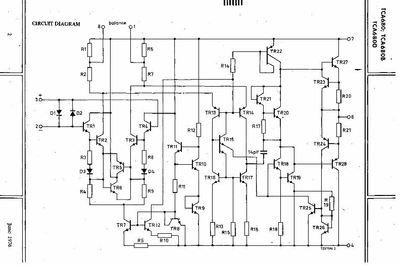
CIRCUIT DIAGRAM 8 balance
r-~~~---1--~--------.-----~--------------------~----------------~~07
+ 30~---'--~---------+~------r-------'
01.Y .. 02 6
20 •
r-------~~~--~--~----~--~--------~~--~--~---.----~-04
~ .n » 0-
~e» nO » ~. o-~ e»n 0» ao-
e» o CI"

II TCA680;TCA680B
TCA680D
RATINGS Limiting values in accordance with the Absolute Maximum System (IEC 134)
Voltages
Positive supply voltage
Negative supply voltage
Common mode input voltage (pins 2 and 3)
Differential input voltage
Current
Vp
-VN
V2-3
max. 18 V
max. 18 V
Vp to -VN
max. ±0,5 V 1)
Input current 12 ; 13 max. ±10 rnA 1)
Temperatures
Operating ambient temperature
Storage temperature; metal envelope
plastic envelope
Power dissipation
Total power dissipation (see derating graph)
750
Ptot (mW)
500
250
o o
,'\ ~
50
, 1\
" ,
r'\ k' " , ~
100
Tamb -25 to +85 °c T stg -65 to +150 oC
T stg -65 to +125 °c
Ptot max. 500 mW
7272812
TCA680
/ TCA680B TCA6800 2)
~
"'~ r\: ~
"
1) Diodes protect the inputs against over-voltage. Therefore, unless current-limiting resistors are used, large currents will flow if the differential input voltage exceeds
.0,6 V. '
2) TCA680D mounted on a ceramic substrate of 5 cm2. When mounted' on a PC-board the maximum power dissipation is 330 mW.
June 1976 II II 3

TCA680; TCA680B II TCA680D
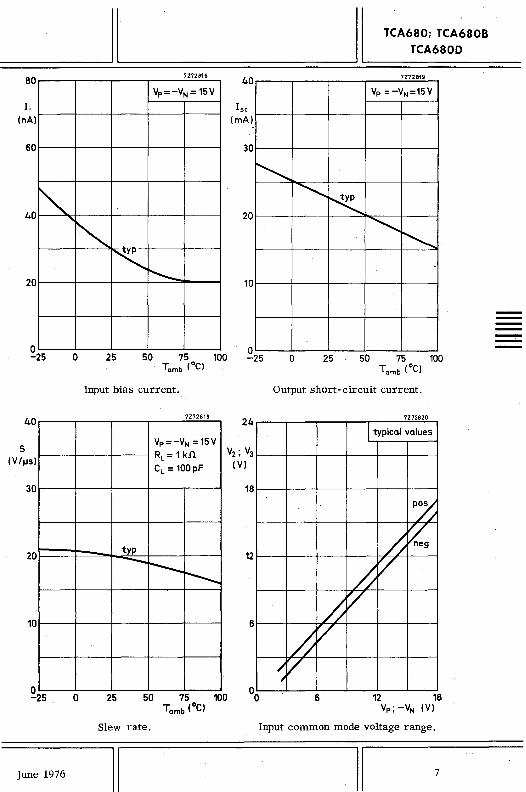
CHARACTERISTICS at Vp = 15 V; -VN = 15 V; Tamb = 25 OC unless otherwise specified
Input offset voltage Vio typo 2 mV < 8 mV
Input offset voltage drift L\.Vio typo 25 mV
Input offset current Iio typo 5 nA < 30 nA
Input bias current I( typo 30 nA < 100 nA
Input voltage range Vi > -12,5 to +13, 5 V typo -13,5 to +14, 5 V
Common mode rejection ratio > 70 dB CMRR 100 dB typo
Power supply voltage rejection ratio PSRR typo 10 'rlV IV < 100 'rlV IV
- Large signal voltage gain - > 30000 - ±V 0 = 10 V; RL = 1 kQ Gv ' - typo 100 000
Output voltage swing at RL = 1 kQ > ±I2 V
Vo typo ±I3 V
Output resistance at f = 1 kHz Ro typo 50 Q < 100 Q
Output short-circuit current Isc typo 22 rnA
Supply current Ip;N typo 4 rnA < 6 rnA
Transient response (voltage follower) Vi = 500 mY; RS = IOkQ; RL = 1 kQ CL = 100pF
rise time typo 50 ns overshoot typ., 20 %
Settling time at Vi= 10 V; 0,1% error typo 750 ns
Slew rate at RL = 1 kQ; CL = 100 pF > 15, V /'rlS S typo 20 V /'rlS
A.C. gain at f = 1 kHz Gv typo 6000
3800 to 8200
Unity gain frequency typo 6 MHz
Power bandwidth (gain: -I) Vo(p-p) ~ 20 V; RL = 1 kQ; CL = 100 pF B typo 320 kHz
4 II II June 1976

II CHARACTERISTICS (continued)
Input noise voltage at f = 1 kHz at f = 80 Hz
Input noise current at f = 1 kHz at f = 80 Hz
Offset voltage adjustment circuit:
30
) (p-p) (V)
20
10
" \ I \
typ
Vn V· n
In In
1\ 1\
" "\ '"
Output voltage swing versus frequency 0
June 1976 II
typo typo
typo typo
.....
II
TCA680; TCA680B TCA680D
25 nV;VH.;, 35 nV;VB.;,
2 pAf'/H;. 4 pAf'/H;.
7Z67592
III II JII I I II
Vp= l5V VN:::::15V RL=2kQ CL:::::100pF
10 7 f (Hz) 108
5

0\
'-I
~ ~ \0 -...] 0\
100
Gv (dB)
60
40
20
o
-20 10
""""""-
......
""
102
UIUII
......
" -
""""""- ...... ......
gain
""""""- r-.... r-..
""""""-I".: phase ...... ~ '" ~
..... 1""-...... I' .......
I'
I CL=100pF t-" 111111 I
II III I I r Tfr I
103 104 105 106
Open -loop voltage gain and phase response versus frequency
7Z67S93
II I Vp=lSV
-VN=lSV RL=lkQ
,
"" --1 CL =( ./
~ , ' ...
o
-tI) Q) Q)
60 ~ Q) tI) C1j
-a
-90
-180
-270
107 f (Hz) 108
-c
~ -cOnco »0 0- ~ •. CO-c on c»
0-co o CIII
II 80 7Z72816
Vp=-VN = 15V
60
'" '" ~ 40
20
o -25
40
5 (V/.,.s)
30
20
10
o
o
-25. 0
June 1976
"--
25
Input bias current.
7Z72818
Vp=-VN = 15V
RL = 1 kn CL = 100pF
typ ---r-----r-----
25
Slew rate.
II
40
Isc (rnA)
30
TCA680; TCA680B TCA680D
7Z72819
Vp =-VN=15V
~
20
10
o -25
24
18
12
6
'" ~ '" ~
o 25 50 75 100 Tamb (oC)
Output short-circuit current.
7Z72820
I typical values
Ph /J ~
/J V
/J V
h V / V I
6 12 18 Vp; -VN (V)
Input common mode voltage range.
II 7
-
--~ -"""'--
tCA680; TCA680B TCA680D
8
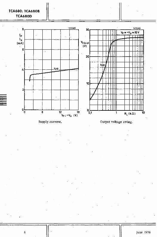
Ip IN
(rnA)
6
4 I
( ~ I--
2
o o
I
6
7Z72821
typ -~ ~
12 18 Vp; -VN (V)
,Supply current.
8 II
30
Vol p_p (V)
)
20
10 j
/ lL
o 0,1
1Z72813
Vp=-VN =15V
~
I
IJ If
J typ
II J
/
10
Output vOltage sWing.
II June 1976

102
~ 10
1 10 102
7Z12817
typ
104 105
f (Hz)
10
1\
'" '-10- 2
10 102 103
TCA680j TCA680B TCA680D
7Z12814
typ
104 105 f (Hz)
Input noise voltage density. Input noise current densit¥".
June 1976
104~ ____ -r ______ r-~ ______ 7Z_72_81_5~
typical values
Vn(rmsl
(nV/fflz)
103r------r------r------r-.~~
102 10 Hz
80Hz
1 kHz
10~----~--~~------+-----~
source resistance
103 104 105 106
Rs (n)
Total input noise voltage density.
II 9

I
TCA680; TCA680B TCA680D I
7Z72811
I /CL =100 pF
t ~,;O 0,6
I "-~ \ I \
0,4
I \ I \
0,2
o J \ / ~
\ l1' --o 200 400 600 time (s) 800
2
Rs TCA680;B;D
10 kn
Transient response curves and test ~ircuit.
10 II If June 1976

Preliminary
II TDA0301D
OPERATIONAL AMPLIFIER
The TDA0301D is a general purpose opcrDtional amplifier. It is equivalent to the LM30 lA, however, it is mounted in a miniature plastic package. The device is intended for a wide range of applications where adaption of the frequency characteristics is desirable. Feed forward compensation can be applied.
Features
• Frequency characteristics adjustable with external capacitor
• Short-circuit protection
• Large input and output voltage range
• Offset voltage adjustable to zero
• Miniature plastic encapsulation
CONNECTION DIAGRAM
OFFSET ZERO/ FREQ. COMPo
-INPUT
+INPUT
PACKAGE OUTLINE (see general section)
SO-8 (SOT-96A); plastic 8-lead flat pack.
August 197() II
FREQUENCY COMPENSATION
Vp
OUTPUT
5 OFFSET ZERO
7Z75117

flllfli .....
CIRCUIT DIAGRAM 01 08 C 7 »
0 N II . I W
0 -c
II 2
_6
5
TR10
!:P-
~R3 R12~ "'tl
c 1'1
~ (D 1-1
00 TR1H a" M-
I--' 5" '-D R4 R6
p:! -....J 1'1 (]\ '<
4
Preliminary
II TDA0301D
RATINGS Limiting values in accordance with the Absolute Maximum System (lEe 134)
Supply voltage
Differential input voltage
Common mode input voltage
Temperatures
Operating ambient temperature
Storage temperature
Junction temperature
Power dissipation in free air; T amb = 50 DC
Mounted on a ce,[I'llic substrate of 4 cm2
derating factor for T amb > 50 °e Mounted on PC board of 4 cm2
derating factor for T amb > 50 oc
2
3
Vp-Vr-..:
Vl+- VI-
VI+; V!_
Tamb
T stg
T· J
Ptot fIRth
Ptot l/Rth
Offset voltage adjust circuits.
R2 Rl
V,_ V 1_
R3 V,+
max. 36 V
max, t:j() V
VN to Vp
-25 to +85 °e -65 to +125 °c max. 125 °C
max. 470 mW 6,3 mW/oC
max. 310 mW 4,2 mW/oC
C2
R~
Cl 7275114
Single pole compensation. Feed forward compensation.
August 1976 II 3

TDA0301D
II Preliminary
'CHARACTERISTICSatVp::: -V,r\ ::: 5 to 15 V; Tamb::: 25 oCunless otherwise specified
Parameter Conditions Symbol min. typo max. Unit
Input offset voltage Vio - 2 7,5 mV
Input offset current Iio - 3 50 nA
Input bias current Ii - 70 250 nA
Input resistance Ri 0,5 2 - MQ
Large signal voltage gain Vp = -VN ::: 15 V; Vo=±1OV;RL~2kQ Gv 25 160 - V/mV
Supply current Vp = -VN = 15 V Ip;N - 1,8 3 rnA
CHARACTERfSTICS at Vp = -VN ::: 5 to 15 V; Tamb ::: 0 to'+70 °C
Parameter Conditions Symbol min. typo max. Unit --- Input offset voltage Vio - - 10 mV
Input offset current Iio - "T 70 nA
Input bias current Ii - - .'300 nA
Average temperature coefficient of V io - 6 30 flV;oe
A verage temperature Tamb ::: 25 to 70 0 C - 0,01 0,3 nA;oC coefficient of Iio T a mb ::: 0 to 125 oC - 0,02 0,6 nA;oC
Input voltage range Vp = -VN = 15 V Vi ±l2 - - V
Common mode rejection ratio CMRR 70 90 - dB
Power supply rejection ratio PSRR 70 96 - dB
. Large signal voltage gain Vp = -VN ::: 15 V; Vo:::±1OV;RL~2kQ Gv 15 - - V/mV
Output voltage range Vp ::: -VN ::: 15 V; RL ::: 10 kQ Vo ±12 ±14 - V RL ::: 2 kQ Vo ±10 ±13 - V
4 II II August 1976

Preliminary
II -TDA0324D
QUADRUPLE OPERATIONAL AMPLIFIER
The TDA0324D consists of four independent, high gain, internally frequency compensated operational amplifiers. It is especially designed to operate from a single power supply over a wide range of voltages. The circuit is equivalent to the LM324, however it is mounted in a miniature plastic package. The device can be directly operated from the standard +5 V supply voltage which is used in digital systems and will easily provide the required interface electronics without requiring the additional ±15 V supplies.
Features
• Internally frequency compensated for unity gain
• Large d. c. voltage gain: 100 dB
• Unity gain bandwidth: 1 MHz
• Wide supply voltage range: 3 to 30 V
• Low supply current drain: 1 mW per op amp at Vp - VN == 5 V
• Differential input voltage range equal to supply voltage
• Input common mode range includes. ground
• Large output voltage range: 0 to Vp - 1,5 V
• Operating temperature: -25 to +85 oc
CONNECTION DIAGRAM OUTPUT (1)
-INPUT (1)
+INPUT (1)
Vp
+INPUT (2)
- -INPUT (2)
OUTPUT (2)
PACKAGE OUTLINE (see general section)
50-14; plastic 14-lead flat pack.
August 1976 II
OUTPUT (4)
-INPUT (4)
+INPUT (4)-
VN (GND)
+INPUT (3)
-INPUT (3)
OUTPUT (3)
7Z75104

'lDA0324D II
Preliminary
CIRCUIT DIAGRAM (one amplifier)
100 6
-INPUTS,
OUTPUT
+
7Z7-2B47
RATINGS Limiting values in accordance with the Absolute Maximum System (IEC 134)
Supply voltage Vp - VN max. 32 V
Differential input voltage
Common mode input voltage
Output short-circuit to VN (see note)
Temperatures
Operating ambient temperature
Stora:ge temperature
Junction temperature
max. ±32 V
max. -0,3 to+32 V
continuous at T amb = 25°C; V p < 15 V, only one amplifier
Tamb
T stg
T j
-25 to +85
-65 to +125
max. 125
°C
°c
°c
Power dissipation in free air; Tamb = 50 OC(see note)
Mounted on a ceramic substrate of 4 cm2
derating factor for T amb > 50°C
Mounted on PC board of 4 cm2
derating factor for T amb > 50,oC
max.
max.
500 mW 6, 7 mW/oC
360 mW 4,8 mW/OC
Note: Short-circuits from the output to Vp can cause excessive heating and eventual destruction. 10 max. is about 40 rnA independent of the magnitude of Vp. -f.-t values of Vp in excess of +15 V, continuous short-circuits can exceed the power dissipation ratings and cause eventual destruction. _. ,
2 II . August 1976

Preliminary
II
TDA0324D
CHARACfERISTICS at Vp = +5 V; VN = 0; T amb = 25 0C unless otherwise specified
Parameter Conditions Symbol min. typo max". Unit
Input offset voltage Vio - 2 7 mV
Input offset current Iio - 5 50 nA
Input bias current 1) Ii - 45 500 nA
Common mode input vo~tage Vp :$ 30 V 2) Vi 0 - Vp- I ,5 V
Common mode rejection ratio d.c. CMRR - 85 - dB
Power supply rejection ratio d.c. PSRR - 100 - dB
Amplifier to amplifier f = 1 kHz to 20kHz - -120 - dB coupling (input referred)
Large signal voltage gain RL > 2 kQ Gv - 100 - V/mV
Output voltage range RL > 2 kQ Vo 0 - Vp-I,5 V
Output current source VI+ = 1 V; VI- =OV 10 20 40 - rnA
, Output current sink Vl+ = OV; VI_=IV 10 10 20 - rnA
Supply current RL = 00 (all op amps) Ip - 0,8 2 rnA
1) The direction of the input current is out of the IC due to the p-n-p input stage.
2) Either input signal voltage should not be allowed to go negative by more than 0,3 V. The upper end of the common mode voltage range is Vp -1,5 V, but either or both inputs can go to +30 V without damage.
August 1976 II 3


. Preliminary
II
TDA0358D
DUAL OPERATIONAL AMPLIFIER
The TDA0358D consists of two independent, high gain, internally frequency compensated operational amplifiers. It is especially designed to operate from a single power supply over a wide range of voltages. The circuit is equivalent to the LM358, however it is mounted in a miniature plastic package. The device can be directly operated from the standard +5 V supply voltage which is used in digital systems and will easily provide the required interface electronics without requiring the additional ± 15 V supplies.
Features
• Internally frequency compensated for unity gain
• Large d. c. voltage gain: 100 dB
• Unity gain bandwidth: 1 MHz
• Wide supply voltage range: 3 to 30 V
• Low supply current drain: 1 mW per op amp at Vp - VN== 5 V
• Differential input voltage range equal to supply voltage
• Input common mode range includes ground
• Large output voltage range: 0 to Vp - 1,5 V
• Operating ambient temperature: -25 to +85 °C
CONNECTION DIAGRAM
OUTPUT (1)
-INPUT (1)
+INPUT (1)
PACKAGE OUTLINE (see general section)
SO-8 (SOT-96A); plastic 8-lead flat pack.
August 1976 II
Vp
OUTPUT (2)
-INPUT (2)
+INPUT (2)
7Z75106

---
TDA0358D
II CIRCUIT DIAGRAM (one amplifier)
100 6 p.A j;.A
INPUTS
+
50 p.A
7272847
-Preliminary
Vp
OUTPUT
RATINGS Limiting values in accordance with the Absolute Maximum System (IEC 134)
Supply voltage
Differential input voltage
Common mode input voltage
Output short-circuit to VN (see note)
Temperatures
Operating ambient temperature
Storage temperature
Junction temperature
VP-VN
VI+ ~ VI
VI+; VI-
max.
max.
32 V
±32 V
-0,3 to +32 V
continuous at T amb = 25 °C Vp < 15 V, oply one amplifier
Tamb
T stg
Tj
-25
-65
max.
to +85 °C
to +125 °C
125 °c
Power dissipation in free air; Tamb = 50 QC (see note)
. Mounted on a ceramic substrate of 4 cm2
derating factor for T amb > 50 00
Mounted on PC board of 4 cm2
derating factor for T a~b > 50 °C
Ptot l/Rth
Ptot l/Rth
max.
max.
450 mW 6 mW/oC
310 mW 4,2 mW/oC
Note: Short-circuits from the output to Vp can cause excessive heating and eventual destruction. 10 max. is about 40 rnA independent of the magnitude ofVp. At values of . Vp in excess of +15 V, continuous short-circuits can exceed the power dissipation ratings and cause eventual destruction ..
2 II August 1976

Preliminary
II TDA0358D
CHARACTERISTICS at Vp = +5 V; VN = 0; T amb = 25 OC unless otherwise specified
Parameter Conditions Symbol min. typo max. Unit
Input offset voltage Vio - 2 7 mV
Input offset current Iio - 5 50 nA
Input bias current 1) Ii - 45 500 nA
Common mode input voltage Vp :5 30 V 2) Vi 0 - Vp-l,5 V
Common mode rejection ratio d.c. CMRR - 85 - <;lB
Power supply rejection ratio d.c. PSRR - 100 - dB I
Amplifier to amplifier f = 1 kHz to 20 kHz -120 dB - -
coupling (input referred)
Large signal voltage gain RL > 2 kQ Gv - 100 - V/mV
Output voltage range RL > 2 kQ .va 0 - Vp-l,5 V
Output current source V 1+ = 1 V; V 1- = 0 V 10 20 40 - rnA
Output current sink VI+ = 0 V; VI - = 1 V 10 10 20 - rnA
Supply current R L = 00 (all op amps) Ip - 0,5 1,2 rnA
1) The direction of the input current is out of the IC due to the p-n-p input stage.
2) Either input signal voltage should not be allowed to go negative by more than 0,3 V. The upper end of the common mode voltage range is Vp - 1,5 V, but either or both inputs can go to +30 V without damage.
August 1976 II II 3

II TDA0741D
OPERATIONAL AMPLIFIER
TheTDA0741D is a silicon monolithic integrated operational amplifier intended for use in hybrid modules and applications where small outline dimensions are important.
Features:
- n9 frequency compensation required - short-circuit protection - large input and output voltage range - offset voltage adjustable to zero
Positive supply voltage
Negative supply voltage
QUICK REFERENCE DATA
Characteristics at T amb = 25 °C
Voltage gain at RL = 2 kQ; V 0 = ±10 V
Common mode rejection ratio
Differential input resistance
Output voltage swing at R L = 10 kQ
Input voltage range
Gv
C:MRR
Ri
Vo
Vi
typo
typo
typo
>
>
15 V
15 V
200 000
90 dB
2 M.Q
±l2 V
±12 V
PACKAGE OUTLINE SOT - 96A (plastic 8-lead flat pack) (see general section).
Tune 1976 II 1

:
TDAO-741D
II II RATINGS Limiting values i~ accordance with the AbSolute Maximum System (IEe 134)
Voltages
Positive supply voltage
Negative supply voltage
Common mode input voltage 1)
Differential input v'Oltage
Power dissipation (see derating curve below)
Total power dissipation (free air, T amb = 50 oc) mounted on a ceramic substrate (4 cm2)
mounted on printed-circuit board. (4 cm2)
Output short-circuit duration 2)
Temperatures
Vp max.
-VN max.
Vi max.
V2-3 max.
max.
max.
indefinite
18 V
18 V
±15 V
±30 V
470 mW,
310 mW
Operating ambient temperature see derating curve below Ta'mb
T stg
-25 to +85 0C
Storage temperature
500
Ptot (mW)
250
o o so
" l-' /' X ~
1'00.. ,/' I'
-65 to +125 oC
7Z73979
I I I I I I I I , , I , I , I I I I I I I
on ceramic substrate -r-'-
I I I I I I I 11 J I I I I I I I I I
'I ~ onpri nted.."ci rc u it' board
r\.. I\.
1'0.. "
, '-..... "-~ ,
1) For supply voltage less than'±15 V, the absolute maximum input voltage is. equal to the supply voltage.
2) Continuous short circuit is aJlowed to ground or either supply.
2 II II June 1976

II CIRCUIT DIAGRAM
2
R9 son
TOA07410
L---~~--~---+---+------~----~--~----~------~-04 7255498.1
5
June 1976 II II 3

TOA07410
II CHARACTERISTICS at Vp = 15 V; -VN = 15 V; Tamb = 25 0C unless otherwise specified
Input offset voltage Vio typo 2 mV < 6 mV
Input bias current Ii typo 80 nA < 500 nA
Input offset current I,io typo 20 nA < 200 nA
> ±12 V Input voltage range Vi typo ±13 V
> 70 dB Common mode rejection ratio CMRR
typo 90 dB
> 0,3 MQ Differential input resistance Ri typo 2,0 MQ
Power s1.lpply voltage rejection ratio PSRR typo 30 flV/V < 150 flV/V
Voltage gain at RL = 2 kQ; Vo = ±10 V > 20000
Gv typo 200000
> ±10 V Output voltage swing ,at R L = 2 kQ Vo typo ±13 V
> ±12 V at RL = 10 kQ Vo typo ±13 V
Output resistance at f = 1 kHz Ro typo 60 Q
Output short-circuit current Isc typo 25 rnA
Suppl)' current at 10 = ,0 Ip;N typo 1, 7 rnA < 2,"8 rnA
Transient response (unity gain; voltage follower) Vi = 20 mY; RL = 2 kQ; CL = 100 pF Rise time typo 0,3 fls Overshoot typo ~ %
Slew rate (unity gain) at R L = 2 kQ S' typo 0,5 V/fls
4 II "
June 1976

II II TDA0741D
CHARACTERISTICS at Vp = 15 V; -VN = 15 V; T amb = 0 to 70 °C unless otherwise specified
Voltage gain at RL = 2 kQ; Vo = ±lOV.
Input offset voltage
Input bias current
Input offset current
Output VOltage swing at R L = 2 kQ
2
3
Vp
7
TDA0741D 6
4
7Z55590.A
Offset voltage zeroing circuit
Vp
7
2
TDA07410 3
Transient response test circuit
June 1976 II
Gv > 15000
Vio < 7,5 mV
Ii < 0,8 f-1A
lio < 0,3 f-1A > ±10 V
Vo typo ±l3 V
II 5


II II TDA0748D
OPERATIONAL AMPLIFIER
The TDA0748D is a high-performance, silicon, monolithic, operational amplifier foruse in a wide range of analogue applications. The device is mounted in a microminiature envelope, especially designed for use in thick and thin -film circuits. Ability to accept a large common mode voltage, together with freedom from latch-up, makes it an ideal voltage follower. Owing to its high gain and wide operating voltage range, it also offers superior performance in integration, summing, and general feedback applications. Features: - suitable for use in thick and thin-film hybrid circuits - short-circuit protection - offset voltage null capability - large common -mode and differential voltage ranges - low power consumption - no latch-up
The TDA0748D is equivalent to fJA 748. It is similar to TBA221D, which has internal frequency compensation.
QUICK REFERENCE OAT A
Positive supply voltage
Negative supply voltage
Characteristics at T amb = 25 °C
Voltage gain at Ri ~ 2 kQ; Vo = ± 10 V
Common mode rejection ratio at RS ::S 10 kQ
Input resistance
Output voltage swing at RL ~ 10 kQ
Input voltage range
Total power consumption
PACKAGE OUTLINE
Gv
CMRR
Ri
±Vo
±Vi
Ptot
SOT - 96A (plastic 8-lead. flat pack) (see general section).
June 1976 II
typo
typo
typo
typo
typo
>
>
typo
II
15 V
15 V
150 000
90 dB
2 MQ
12 V
12 V
60 mW
-----

--
TDA0748D
II 11 CIRCUIT DIAGRAM
2 8
r-~~--~--~----+---+-----~~~~~------------------+--n7
02
R5
6
5 TR10
TR15
R1 03 04 R7
~--~~~-------+----~--~--~~~--~--------+-----------~-O4 7Z68979
RATINGS Limiting values in accordance with the Absolute Maximum System (IEC134)
Voltages
Positive supply voltage Vp max. 18 V
Negative supply voltage VN max. 18 V
Common mode input voltage ± Vi max. 15 V 1)
Differential input voltage ± V2-3 max. 30 V
----. Total power dissipation up to T amb = 50 oC Ptot max. 470 mW 2)
Output short-circuit duration max. 60 s
1) For supply volt[Lge less than ± 15 V, the absolute maximum input voltage is equal to the supply vo1t:-lge.
3)
2) When soldered on a ceramic substrate. In free air the maximum di,ssipation is 31OmW.
3) Short circuit is allowed to ground or either supply during this period.
2 II II June'1976

II II TDA0748D
RATINGS (continued)
Temj2eratures
Storage temperature T stg -55 to +125 °c
Operating ambient temperature Tamb o to +85 °c --Lead temperature (soldering time < 60 s) Tlead max. 260 °c
CHARACTERISTICS Vp = 15 V; VN = 1'5 V; Tamb = 25 °C; C == 30 pF unless otherwise specified
Inj2ut offset voltage at RS =s 10 kQ Vio typo 2,0 mV < 6,0 mV
Input offset current Iio typo 20 nA < 200 hA
Input bias current Ii typo 80 nA < 500 nA
> 0,3 MQ -Input resistance Ri -typo 2,0 MQ
In put capacitance Ci typo 2,0 pF
Offset volta~ adjustment ran~ ± Vio typo 15 mV
> 20000 Large signal voltage gain at RL ~ 2 kQ; ± V 0 == 10 V Gv typo 150000
Output resistance Ro typo 75 Q
Ouq~ut short-circuit current Isc typo 25 rnA
Supply current Ip;N typo 1,9 rnA < 2,8 rnA
Total power consumption Ptot typo 60 mW < 85 mW
Transient response at Gv == 1 (voltage follower)
Vi = 20 mV; C = 30 pF; RL == 2 kQ CL =s 100 pF
rise time tr typo 0,3 Il s
overshoot typo 5,0 % Slew rate at Gv == 1 (voltage follower); RL ~ 2 kQ S typo 0,5 V/lls
Transient response at Gv == 10 (voltage follower)
Vi == 20 mV; C == 3,5 pF; RL == 2 kQ CL::S 100 pF
rise time tr typo 0,3 IlS -overshoot typo 5,0 %
Slew rate at Gv = 10 V (voltage follower) ; RL ~ 2kQ S typo 5,5 V IllS
June 1976 II II 3
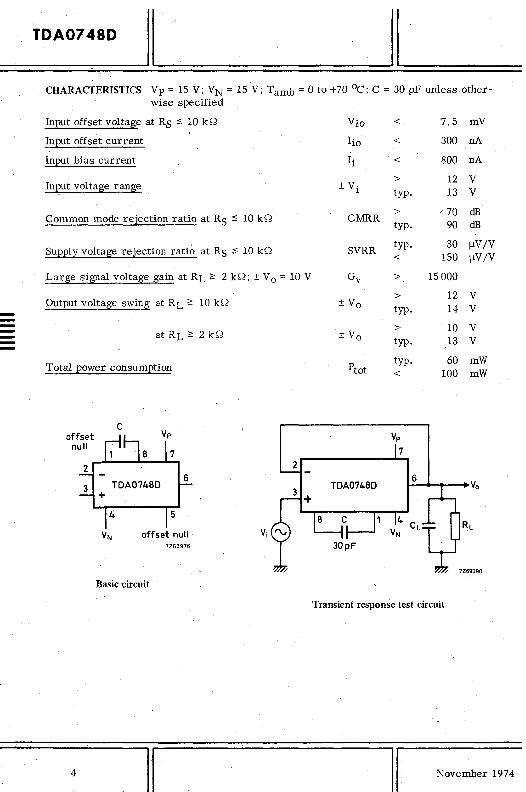
TDA0748D
II II CHARACTERISTICS Vp = 15 V;'VN = 15 V; Tamb = 0 to +70 °C; C = 30 pF unless other-
wise specified
Input offset voltage at RS :5 10 kQ Vio < 7,5 mV
Input offset current Iio < 300 nA
Input bias current Ii < 800 nA
In~ut voltage range > 12 V
± Vi typo 13 V
Common mode rejection ratio at RS :S 10 kQ CMRR > , 70 dB typo 90 dB
Supply voltage rejection ratio at RS :S 10 kQ 1 SVRR typo 30 ~V/V < 150 ~V/V
Large signal voltage gain at RL <:: 2 kQ; ± Vo = 10 V Gv > 15000
Output voltage swing at RL <:: 10 kQ > 12 V
±Vo 14 V typo
- > 10 V - at RL <:: 2kQ ±Vo typo 13 V
Total power consumption Ptot typ .. 60 mW < 100 mW
C offset Vp
null 7 7
2 2
TDA0748D 6
3 +
TDA0748D 6
Vo 3
+ 5
CL RL VN offset null
7Z68976 30pF
Basic circuit
Transient response test circuit
4
11 11 November 1974

II II TDA0748D
Offset voltage null circuit
Vp
4
2 6
3 TDA0748D +
3 TDA0748D +
6
5
~S"Mn ~ "'""
Recommended circuit Alternate circuit
-
7Z 701 111 10 7Z70182
200 Vp =VN=15V r-r- Vp =VN =15V
"-....... ~
........ i'o..
...... r--., typ 1'0 ...... -r-- -..
100
5
)1 I
II typ
)1 )1
)~
II 1I
4
3
2
o 1 o 25 o
November 1974 II II 5

----
TDA0748D
35
lsc
(rnA)
30
2.5
20
15
40
I io
(nA)
30
20
10
i'oo.
o
i'oo.
o o
6
~ ...... ~
.......
25
i" ..... -I"-~
25
.......
-
II
7Z70180
Vp =Vfoj=15V I-- -..,..
""
- - f------
typ ...........
r-.... ......
........ ~
- 7Z70179
Vp =VN =15V I---
~p
30
lio
(nA)
20
10
125
Gv (dB)
100
75
50 50 75 0
T amb (OC)
II ?Z70177
I I I I I I I I II Tamb= 25°C -t-
I I I
typ
"""I""" ~
10 Vp; VN (V) 20
7270116
I I I I I I I Tamb=25°C 1---
RL=2kn 1--'-
"",,-
~
.I .... .... typ , ,
10
II November 1974

60
Vo(p-p) (V)
40
20
o o
150
Ptot (mW)
100
50
o o
November 1974
II
1/ 1/
/ 1/
I..., /
I'"
II
?i?01? 5
11111 ~ I~J
Tamb=2S0C 1-1-
RL=2kfi f--
/ IL
/ 1/
1/ /
typ / :;f
/ /
/
10 Vp;VN (V) 20
72?01?4
I I I I I I I Tamb=2soC f--
RL=oo 1--
II
/
/
/ J
ty~ 1/
~
10 Vp; VN (V) 20
15
I-r-
10
5
30
20
10
o 10-1
I I I I I I I
Tamb =2soC
i
-1
J 'I
J 'I
j rf
~
I I
I ~
J / ~
I
II TDA0748D
?Z70176 .--
'I J
II
/
If j
/ typ
/
1
------10 Vp;VN(V) 20
7Z?0183
./ typ
Vp =VN =1sV
Tamb=25°C
10
II 7

00
z ~
i 11
I-' \0 -...J ~
125
Gy
(dB)
100
75
50
25
o
-25
I
.......... 1"0,
1 10
I I I
..... ~
~ RL =2kfi
......... ~ C=3pF
RL=2k~ ;...
C=30pF ,...
........ i'..
J ...j
10 2 103
1111111
I
r-
~ .....
..........: 1"0.. ...... ....
........ ~
J /
104 105
7Z70186
11111 I 1 111111 llT Vp=VN=15V Tamb=2SoC Rs =50 .. n . typical v~iues
1"0.: .....
" '" " ~~
106 f(Hz) 107
-I C » o 'I • (1)
c

II'
November 1974" II
o o ~ I
II TDA0748D
II
o o Ll) ..
9

----
TDA074-8D
30
Vo (p-p)
(V)
20
10
o
100
CMRR (dB)
75
so
.25
o
1
1
10
II
10
II
1\
\ C=30pF
\ \ \ \ \ \ \
i\' \.
\.
" I\\.. "
10
r---.~
7Z70185
I I I
Vp = VN= 15V
1\ Tamb=25°C 1\ RL =10kfi
\ \ typical values
\ C=3pF
\ \ \ \ \ \ 1
\ -\.
\..
" '-~
~ ........... ........... I"--..... -"- -...
f (kHz)
7Z70184
IIII Vp =VN =15V Tomb= 25°C C =30pF
~ '",
~
~P ',,-
r-...
~ .... ""-
~
II November 1974
II
OPERATIONAL AMPLIFIER
TOA1034; N TOA1034B; NB TDA10340; NO
The TDA1034 is a high-performance general purpose operational a~plifier. Compared to most of the standard operationa 1 amplifiers (e. g. fJA 741, TBA221, LM301A and LM307), it shows better noise performance, improved output drive capability and considerably higher small-signal and power bandwidth. This makes the device especially suitable for application in high quality and professional audio equipment, in instrumentation and control circuits and telephonechannelamplifiers: The op amp is internally compt;nsated for gain equal to, or higher than, three. The frequency response can be optimized with an external compensation capacitor for various applications (unity gain amplifier, capacitive load, slew-rate, low overshoot, etc.). If very low noise is of prime importance, it is recommended that the TDA 1034N version be used which has guaranteed noise specifications and somewhat lower input current. --Features
• Small-signal bandwidth: 10 MHz
• Output drive capability 600 Q, 10 V (r. m. s.) at Vp = -VN = 18 V
• Input noise voltage 4 nV /\,f"Hz
• D. C. voltage gain 100 000
• A. C. voltage gain 6000 at 10 kHz
• Power b~ndwidth 200kHz
• Slew-rate 13 V /f.is
• Large supply voltage range : ± 3 to ± 20 V
PACKAGE OUTLINES (see general section).
TDA 1034; N : TO-99 (8-lead metal envelope). TDA1034B; NB : SOT-97 (plastic 8-lead dual in-line). TDA1034D; NO : SO-8 (SOT-96A) (plastic 8-lead flat pack).
June 197~ II II

tv
'2' g ..... \C -...J 0\
CIRCUIT DIAGRAM 1
+ 3 a • •
D1 D2
2 0 ,
R2
R6
~ "
1111111
8 5
R9
R16
C3
~----...~ , , 7Z72711.1
6
---t ---t ---t CCC ~~~ ............ 000 WWW ~~~ C D:!' .... .... .... Z ZZ CD:!'

II TDA1034j N TDA1034B; NB TDA1034D; NO
RATINGS Limiting values in accordance with the Absolute Maximum System (lEe 134)
Voltages
Pas itive supply voltage Vp max. 20 V
Negative supply voltage VN max. 20 V
Common mode input voltage (pins 2 and 3) Vp to -VN
Differential input voltage V2-3 max. ± 0, 5 V 1)
Temperatures
Operating ambient temperature Tamb -25 to +85 °c
Storage temperature; metal envelope T stg -65 to +150 °c plastic envelope T stg -65 to +125 °C
Maximum power. dissipation in free air
package mounting max. power der<lting max. junction thermal dissipation factor for temperature resistance atT amb = 50,oC Tamb>50 oC Rth j-a
(mW) (mW JOC) (oC) (OC/W)
on PC board 625 6,25 150 160 TO-99
with 33 °c /W cooling fin; on PC board
1100 11 150 90
SOT-97 on PC board 450 6 125 165
on ceramic 500 6,7 125 150
SOT-96A substrate of 4 cm2
on PC board of 4 cm2 325 4,3 125 230
1) Diodes protect the inputs aga inst over- voltage. Therefore, unless current-limiting resistors are used, large currents. will flow if the differential input voltage exceeds 0,6 V.
June 1976 II

TDAlO3.4;'N
II TDA1034Bj NB 'TDA1034D; NO,
CHARACTERISTICS atVp=;:15V;-VN = 15 V; Tamb =25 °C ldnless otherwise specified
Input offset voltage Vio typo 0,5 mV < 4,0 mV
Input bias current Ii typo 0,5 . ~ < 1,5 ~
Input offset current Iio typo 0,02 ,~ < 0,3 ~
> +12; -13 V Input voltage range Vi typo +13; -14 V
Ri > 30 k.Q
Differential input resistance typo 100 k.Q
> 80 dB Common mode rejection ratio CMRR
100 dB typo
Power supply voltage rejection ratio PSRR typo 10 flV/V < 50 flV/V - Large-signal voltage gain > 30000 - R L = 600 Q; V 0 = ± lOY Gv typo 10nOOO
> ±12 V Output voltage swing at R L = 600 Q Vo typo ± 13 V
Output' res istance; closed loop Gv = 30 dB; f = 10 kHz; R L = 600 Q; Cc = 22 pF Ro typo 0,3 Q
Output short-circuit current Isc typo 38 rnA
typo 4 rnA Supply current at 10 = a Ip; N < 6,5 rnA
Transient response (voltage follower) Vi = 50 mY; RL = 600 Q; Cc = 22 pF;C L = 100 pF
rise time tr typo 20 ns overshoot typo 20 % Vi = 50 mY; RL = 600 Q; Cc =,47 pF; CL = 500 pF
rise time tr typo 50 ns overshoot typ. 35 %
A.C. gain at f = 10 kHz; Cc = a Gv typo ,6000 at f = 10 kHz; Cc = 22 pF Gv typo 2200
Unity gain frequency at Cc = 22 pF; CL = 100 pF typo 10 MHz
Slew-rate at Cc = 0 S typo 13 V /fls at Cc = 22 pF S typo 6 V /fls
Power bandwidth at V o(p-p) = 20 V Cc = a . B typo 200 kHz Cc = 22 pF B typo 95 kHz
4
II June 1976

II CHARACTERISTICS (continued)
Input noise voltage at f = 30 Hz at f = 1 kHz
Input noise current at f = 30 Hz at f = 1 kHz
Vn typo
Vn typo
In typo
In typo
TOA1034; N TOA1034B; NB TOA1034D; NO
7 nV;....;-fu 4 nV;'i"Hz
2,5 pA;\[H;, 0,6 pA;'i"Hz
CHARACTERISTICS atVp = 18V; -VN = 18 V; T amb = 25 OC unless otherwise specified
Output voltage swing at R L = 600 Q > ± 15 V
Vo typo ± 16 V
Supply current at 10 == 0 Ip;N typo 4,2 rnA < 7 rnA
Power bandwidth at Vo(p-p) = 28 V R L = 600 Q; Cc = 22 pF B typo 70 kHz
TDAI 034N version
The TDA 1031N version has the same electrical specifications as the TDA 1034, with the following exceptions:
Inpu t bias current
Input offset current
Input noise voltage at f = 30 Hz
at f = 1 kHz
Input noise current at f = 30 Hz at f = 1 kHz
Broadband noise figure f = 10 Hz to 20 kHz; RS = 5 kQ
Frequency compensation and offset voltage adjustment circuit.
June 1976 II
Ii
lio
Vn
Vn
In In
F
typo 0,4 fJA < 0,8 fJA typo 0,01 fJA < 0,2 fJA typo 5,5 nV;'v'lli < 7 nV;Vlli
typo 3,5 nV;\[H;, <: 4,5 nV /Vlli
typo 1,5 pA;\fj:h typo 0,4 pA;v'"lli
typo 0,9 dB
5

TDA1034B;NB . IUAIU~4; ~ I
. TDA1034D;ND '.
~
E
r
120
G ... (dB)
80
40
o
'\
7Z72709
I typical values
~ '\ ~=O Cc=22~ ~
~ ~ I~
-4010 102 103 104 105 106 107
60
Gv (dB)
40
20
o
f (Hz)
Open loop frequency response.
7Z72108
typical values
Cc=O; RF=10kfl; RE =100n
\ Cc=O; RF = 9 kfl; RE= 1 kfi
\ Cc = 22pF; RF= 1kfi; RE = 00
1\ 107 108
f (Hz)
6
II
16
S (V/~s)
12
8
4
II ·7Z72105
Vp =-VN=15 V
1\ ~ 1\ \
.\ \
'" ~yp '" ~ I'"'---.. 40
Cc(pF) 80
Slew-rate as a function of compensation capacitance.
Cc
7Z72713
Closed loop frequency response.
II June 1976

1,4
1,2
0,8
'" 0,4
o ...:25 o
II 40~ __ ~ ____ ~ __ ~ ____ ~1Z~12~10~4~
Vp =-VN=15V
Vo(p_pl t--_-+ __ -+-_--l_"t_Y_Pi_CQ_'r-v_Q_'u_es-I (V)
30t----+----+-----l--~-~
20t----+--+--~~~~-~
10r---+--~-__l~_+~---1
O~--~----~--~~--~--~ 102 103 104 106 107
f (Hz)
Large-signal frequency response.
1Z72702
Vp =-VN =15V 80
10 (mA)
60
~ ~
I u"'lu.)~i 1'41
TOA1034Bi NB TOA1034Dj NO
7Z72703
Vp =-VN =15V
--
-I----~
40
............... ~ ~ -
"
25 50 75 100 Tamb (oCI
20
o -25 o 25
.... -
50 75 100 Tamb (oC)
Input bias cur~ent~ Output short-circuit current.
June 1976
II 7

------
• ""·'''v~~i .,
to"Al034B; NB TOA1034:D; ND
30
20
10 1/ ~~
1I"1~
7Z72700.1
typical values
neg,;~ IA
lAY ~rl
~ POS-I-~
~
II"I~ [,I"l~
,~
"""~ iI'"
/ /
o ,
o 10 Vp;-VN (V) . 20
Input common mode voltage range.
8
6
Ip IN
(rnA)
4
2
o o
II • 7Z72699.1
'0= 0
,
typ """ .... .... 1-""'" -.... ~ -""" ....
10, Vp; -VN (V) 20
Supply current.
11 ,June 1976

II 102 7Z72707
TDA1034N -
Vn(rms) Inlrms)
TDA1034; N TDA1034Bj NB TDA1034Di' ND
7Z72706
TDA1034N
(nv/lHi) (pA/IHZ)
~ - typ
10
10-1
10-2 10
106
Vn(rms)
:nV/fHz)
105
10
103 104 f (Hz)
Input noise voltage density.
7Z72710
TDA1034N typical values
'12:'
/ ~ ~~ V '/ ~
7 ~thermal noise of source resistance
V
-105 106 104
Rs (n)
Total input noise density.
June 1976 II
10
~
1
10-2 10
'" ~
102 103 104 f (Hz)
Input noise current density.
102r-________ -r~------,_-7-Z7-27-01~ TDA1034N
typical values Vnlrms) /------r---' (~N)
10r----r---~-----~_.~_;
10-1 r-----r---~------_t_---__I
10-2~----~----~~----~----~ 102 103 104 105 106
Rs (n)
Broadband input noise voltage.
9

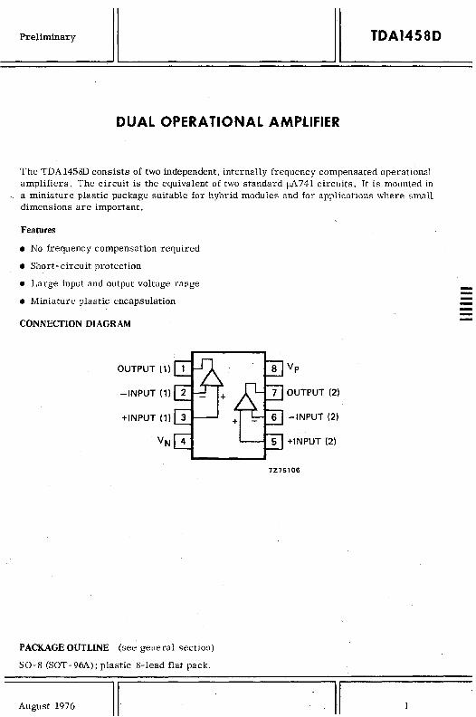
Preliminary
II TDA1458D
DUAL OPERATIONAL AMPLIFIER
The TDA 1458D consists of two independent, internally frequency compensated operational amplifiers. The circuit is the equivalent of two standard fJA 741 circuits. It is mounted in
, a miniature plastic package suitable for hybrid modules and for applications where small dimensions are important.
Features
• No frequency compensation required
• Short-circuit protection
• Large input and output voltage range
• Miniature plastic encapsulation
CONNECTION DIAGRAM
OUTPUT (1)
-INPUT (1)
+INPUT (1)
PACKAGE OUTLINE (see general section)
80-8 (SOT-96A); plastic 8-1ead flat pack.
August 1976 II
Vp
OUTPUT (2)
-INPUT (2)
+INPUT (2)
7Z7S106
II
--

N
>C
~ ~ t\0 -...l 0\
CIRCUIT DIAGRAM (one amplifier)
INPUT
R1
~---~ , . ~
30pF
D1
TR13
R6
1111111
,
OUTPUT
R7
7 Z75089
-I C » -.,. VI 00 C
~ Cl> ..-8 S' Il> t-t
'<

Preliminary
II TDA1458D
RATINGS Limiting values in accordance with the Absolute Maximum System (IEC 134)
Supply voltage Vp -VN max. 36 V \
Differential input voltage Vl+ - VI- max. ±30 V
Common mode input voltage VI+; V!_ VN to Vp
Temperatures
Operating ambient temperature Tamb -25 to +85 °C
Storage tempen\.ture Tstg -65 to +125 °C
Junction temperature Tj max. 125 °C
Power dissipation in free air; T amb = 50 OC
Mounted on a ceramic substrate of 4 cm2 Ptot max. 480 mW derating factor for T amb > 50 °C 1/Rth 6,4 mW/oC
Mounted on PC board of 4 cm2 Ptot max. 325 mW -derating factor for T amb > 50 0C 1/Rth 4,3 mW/oC ----
August 1976 II II 3

TDA1458D
II Preliminary
CHARACTERISTICS at Vp = 15 V; -VN = 15 V; Tamb = 25 0C unless otherwise specified
Parameter Conditions Symbol min. typo max. Unit
Input offset voltage Vio - 2 6 mV
Input offset current lio - 20 200 nA
Input bias current Ii - 80 500 nA
Input voltage range Vi ±12 ±13 - V
Common mode rejection ratio CMRR 70 90 - dB
Differential input resistance Ri 0,3 1 - MQ
Power supply rejection ratio PSRR - 30 150 IlV /V Large signal voltage gain RL =2 kQ; Vo =± lOY Gv 20 100 - V/mV
Output voltage swing RL=lOkQ Vo ±12 ±14 - V RL = - 2 kQ Vo ±10 ±13 - V -- Output resistance f = 20 Hz Ro - 300 - Q
Output short-Circuit current Isc - 20 - mA
Supply current 10 = 0 Ip; IN - 2,3 5,6 rnA
Power bandwidth gain = I;RL = 2 kQ; THO<5%;Vo(p_p) =20V B - 14 - kHz 1)
Unity gain cross -over freqIJency open loop - 1,1 - MHz
Phase margin - 65 - degree
Gain margin - 11 - dB
Slew rate RL="2kQ S - 0,8 - V Ills
Channel separation - 120 - dB
CHARACTERISTICS at V P = 15 V; -V N = 15 V; T amb = 0 to +70 °C
Parameter Conditions Symbol min. typo max. Unit
Large signal voltage gain R L = 2 kQ; V 0 =± 10 V Gv 15 - - V/mV
Input offset voltage Vio - - 7,5 mV
IJ;l.put offset current Iio - - 300 nA
Input bias current Ii - - 800 nA
Output voltage swing RL = 2 kQ Vo ±10 ±13 - V
1) THO = total harmonic distortion.
4 II 11

DEVELOPMENT SAMPLE DATA This information is derived from development samples made available for evaluation. It does not form part of our data handbook system and does not necessarily imply that the device... will go into production
TDA4250B TDA4250D
PROGRAMMABLE OPERATIONAL AMPLIFIER
The TDA4250B; 0 is a versatile, programmable monolithic operational amplifier, especially designed for applications requiring very low stand-by power consumption over a wide range of supply voltages. The quiescent current of the amplifier can be set by a single external resistor or current source. With this programming, the power consumption, input current; slew rate and gain-bandwidth product can be adapted to a particular application. The TDA4250B is mounted in a standard plastic 8-lead dual in-line. The TDA4250D is mounted in a miniature plastic encapsulation, mainly intended for use in hybrid circuits. The circuit is equivalent to the LM4250; C, SG4250; C, ICL8021 and similar to the ~776; C.
Features
• Programmable electrical parameters
• Very low stand - by power consumption
• No frequency compensation required
• ± 1 to ± 18 V power supply operation
• Short-circuit protection
• Offset voltage adjustable to zero
• Operating ambient temperature': -25 to +85 °c
CONNECTION DIAGRAM
BALANCE
-INPUT
+INPUT
PACKAGE OUTLINE (see general section)
TDA4250B : plastic 8-lead dual in-line. TDA4250D : SO ~ 8 (SOT - 96A); plastic 8-lead flat pack.
August 1976 II
QUIESCENT CURRENT SET
Vp
OUTPUT
BALANCE
7Z76107
II

-----
TOA4250B TDA4250D
CIRCUIT DIAGRAM
I II
~--------------------------~--~------~----~ 7
r--8o---+-~~-+---------~~-----~
r.t, ~ : Rset y ~.
VN
2
5
2
6
~----~---~--~---+----------~-----------+-----~4
II II August 1976

II TDA4250B TDA4250D
RATINGS Limiting values in. accordance with the Absolute Maximum System (lEe 134)
Supply voltage
Common mode input voltage (pins 2 and 3)
Differential input voltage
Output short-circuit duration
Temperatures
Operating a mbient temperature
Storage temperature
Junction temperature
Power dissipation in free air; T amb = 50 °C
TDA4250B
Mounted on PC board derating factor for T amb > 50 °C
TDA4250D
Mounted on a ceramic substrate of 4 cm2
derating factor for T amb > 50 °C
Mounted on PC board of 4 cm2
derating factor for T amb > 50 0C
CHARACTERISTICS
VP;-VN
VI+; VI-
VI+ - VI-
indefinite
Tamb
T stg
Tj
Ptot l/Rth
Ptot l/Rth
Ptot l/Rth'
7272850
Offset voltage adjustment circuit.
August 1976 II
max. 18 V
Vp to -VN
max. ±30 V
-25 to· +85 °c
-65 to +125 oc
max. 125 °c
max. 440 mW 5,8 mW/OC
max. 470 mW 6,3 mW/oC
max. 310 mW 4,2 mW/OC
II 3
---
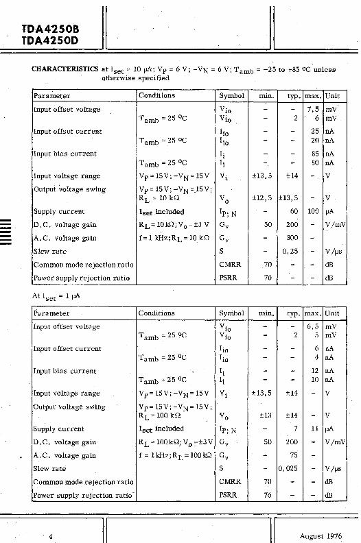
------
TDA4250B TDA4250D
CHARACTERISTICS at Iset = 10 ~; Vp = 6 V; -VN = 6 V; T amb'= -25 to +85 oc unless otherwise specified
Parameter Conditions Symbol min. typo max. Unit
Input offset voltage Vio - - 7,5 mV Tamb = 25 °c Vio - 2 6 mV
Input offset current Iio - - 25 nA Tamb =25 oc Iio - - 20 nA
Input bias current Ii - - 85 nA Tamb = 25°C Ii - - 80 nA
Input voltage range Vp= 15V; -VN = 15V Vi ±13,5 ±14 - V
Output voltage swing Vp = 15V; -VN =.15 V; RL = 10 kQ Vo ±12,5 ±13,5 - V
Supply current Iset .included Ip; N - 60 100 IJA D.C. voltage gain R L= 10 ~; V 0 == ±3 V Gv 50 200 - V/mV
A.C. voltage gain f= 1 kHz;RL = 10 kQ Gv - 300 -Slew rate S - 0,25 ... V /f,ls
Common mode rejection ratio CMRR 70 - - dB
Power supply rejection ratio PSRR 76 - - dB
At Iset ::: 1 IJA
Parameter Conditions Symbol min. typo max. Unit
Input offset voltage Vio - - 6,5 mV Tamb == 25 °C Vio - 2 5 mV
Input offset current Iio - - 6 nA
Tamb = 25 °c lio - - 4 nA
Input bias current Ii - - 12 nA
Tamb == 25°C Ii - - 10 nA
Input voltage range Vp= 15 V;-VN== 15V Vi ±13,5 ±l4 - V
'Output voltage swing Vp == 15V; -VN == ISV; RL=100kQ Vo ±13 ±14 - V
Supply current Iset included Ip; N - 7 11 IJA D . C. voltage .gain RL = 100kQ;V,o =±3V Gv 50 200 - V/mV
A.C. voltage gain f = lkHz;RL == 100 ~ Gv - 75 -
Slew rate S - 0,025 - V/f,ls
Common mode rejection ratio CMRR 70 - - dB
Power supply rejection ratio- PSRR 76 - - dB
4 II II August 1976

TELECOMMUNICATIONS CIRCUITS
------

-. -
TYPE SELECTION
Telecomm~nicatjons circuits
TAA960
TAA970
TBA673
TBA915
TCA210
TCA240
TCA580
TCA770; A; D
TCA980
TDA1022
1 j I
...: triple amp
- microphone amp
- balanced modulator
- audio amp
- audio amp
- balanced modulator
- gyrator
- i. f. amp/f. m. discriminator
- microphone amp
- bucket brigade delay line
II
II November 1976

II II TAA980
TRIPLE AMPLIFIER FOR ACTIVE FILTERS
The T AA960 consists of three identical general-purpose amplifiers integrated in, a single silicon chip. The amplifiers can be used separately or can be cascaded to give a voltage gain of 117 dB. One of the amplifiers has an additional emitter-follower stage. The TAA960 is very suitable for use in an active RC band-pass filter with Q up to 60.
QUICK REFERENCE DATA
Supply voltage V3- 10 . nom. 6 V
Supply current 13 typo ' 2 rnA
Transfer admittance (each amplifier) [Yfsl typo 9.5 mQ-l
Voltage gain (each amplifier) Gv typo 39 dB
Input resistance (on pins 1, 7 and 8) Ri > 25 kQ
Output resistance (on pins 2, 5 and 6) Ro typo 9 kQ
(on pin 4) Ro typo 500 Q
Q factor (in typical RC filter) Q typo 45
PACKAGE OUTLINE 1'0-74; reduced height Dimensions in mm
0.86 max g "n=-S!
I~I_. ------'-!12"-'.!-.7m_ in _.1 7ZSSJ26
December 1970 II II 1
--

TAA980 II RATINGS Limiting values in accordance with the Absolute Maximum System (IEC 134)
Voltages with respect to pin· 10
Supply voltage 1) V3 max. 10 V
Input voltage VS' V7' VI max. 4 V
Output voltage V6' V5' V4, V2 max. 10 V
Currents
Input current . IS, 17, 11 max. 50 jJA
Total12ower dissi12ation Ptot max. 250 mW
T.em12erature s
Storage temperature Tstg -65 to +125 °C
Operating ambient temperature Tamb -55 to + 65 °C
CIRCUIT DIAGRAM. -8 6 7 5 4 2
~------------+------+------------~--~--O10
1) With lower d. c. potential on all other terminals.
2 II II December 1970

II TAA960
CHARACI'ERISTICS at V3 = 6 V; Tamb = 25 °c unless otherwise specified.
Supply current 1) 13
Supply current 1) at V 3 = 10 V 13
Voltage gain (each amplifier) Gv
Input resistance (each amplifier) Ri
Output resistance on terminals 2, 5 and 6 Ro
on terminals 4 Ro
1) Terminal· 8 connected to terminal 6 7 5 1 2
December 1970 II
1. 5 to 2.5 typo 2.0
1. 5 to 3.8 typo 2.6
60 to 150 typo 90
> 25
> 8 typo 9
135 to 750
II 3
rnA rnA
rnA rnA
kQ
kQ
kQ
Q
------

-----
TAA960 II
APPLICATION INFORMATION
Active RC filter for frequencies up to 150 kHz
-. This frequency range can be extended to 200 kHz if a feed forward capacitor is connected between pin 5 and 8.
R
TAA960' .
L- . - • - . - - - - ---;J10· -. -- -- -- . 7:61~ J
R = 10 kQ
Frequency typo 1 21T RC
Supply voltage Vp typo 6 V
Filter performance 40 to 55 at Tamb = 25 bC Q
typo 45 at Tamb = -30 to +65 ~C Q 35 to 55
Input voltage Vi typo 400 mV
Output voltage Vo typo 400 mV
Distortion at V 0 = 350 mV dtot typo 2 %
SIN :ratio at Vo' = 4UU mV SIN > 50 dB
Input resistor 1) RS typo 470 kQ
1) Value of input resistor to be determined for ~~ .. = O,?O to 1,1. . 1
4 II June 1976,

II II TAA970
MICROPHONE AMPLIFIER
• The TAA970 is a monolithic integrated microphone amplifier for use in telephone systems. It is compatible with both piezo-electric and dynamic microphones of suitable impedance and sensitivity, Special features are: - almost constant voltage gain and d. c. voltage drop with supply current variations of
10 to 100 rnA. I
- output voltage before limiting: 1 V (r. m. s. value) - operation is independent of supply voltage polarity - gain can be set to either of two values - only one external capacitor required - output impedance determined by internal feed back
QUICK REFERENCE DATA
Supply current
Supply voltage drop at ± I2 = 50 rnA
Voltage gain pin 9 not connected pin 9 connected to pin 10
Output impedance pin 9 not connected pin 9 connected to pin 10
PACKAGE OUTLINE
TO-74 (reduced height)
November 1974 II
O,86max
-j I=--
9,4max ---
± 12 10 to 100 rnA
±V2-4 typo 4,8 V
Gv typo 150 Gv typo 210
Ro typo 60 Q
Ro typo 100 Q
Dimensions in mm
II
----

----
TAA970 il II CIRCUIT DIAGRAM
r---~------------~--~----------------------~----------~~~~---o4
R5 2k!l
R7 2k!l
Rll
200kO Rl0
L---~----------+---~----+-------~----~----+-----~----~~~~~-o10
7ZSS490.2
2 II November 1974'

II II TAA970
RATINGS Limiting values in accordance with the.Absolute Maximum System (IEC 134)
Currents
Supply current (d. c.)
A. C. component of supply current (peak value)
Pin No.6 current
Pin No.8 current
Power dissipation
Total power dissipation
Temperatures
750
Ptot (mW)
500
250
o
'Storage temperature
-50
Operating ambient temperature
THERMAL RESISTANCE
From crystal to case
From crystal to ambient
November 1974
~ ~
o
I\.
12 -100 to + 100 rnA
12m. max. 100 rnA
16 max. 100 ~
18 max. 100 ~
Ptot max. 700 mW
7Z64879
\
1\ ~'fI );0
~ ~-r----
"'{-, ~ -c-{~~~r-- "\\ r--
" ~ 01-1--' ~-I,\~~~~
/'\ ~~
I\. 1\ ~ \ ~
~
T stg -55 to + 125 °c
Tamb -35 to +75 °c
Rth cr-c 65 °C/W
Rth cr-a 180 °C/W
II 3
----

--
lAA970
II II CHARACTERISTICS at RL = 200 Q; f = 2 kHz; T amb = 25 0C unless otherwise specified.
(see test circuit below).
Supply voltage drop at Rth j-a = 100 °C/W
± 12 = 10 rnA
±12 = 50 rnA
-± 1Z = 100 InA
V oltage gain
pin 9 not connected ±12 = 10 rnA
± 1Z = 50 rnA
pin 9 connected to pin 10
Change of voltage gain
when changing T amb from -20 °C to + 55 °c
Gain reduction at f = 300 Hz
(with respect to f = Z kHz)
Output impedance at ± 12 = 50 rnA
pin 9 not connected
pin 9 connected to pin 10
Noise output voltage at B = 0,3 kHz to 4 kHz
pin 9 not connected
pin 9 connected to pin 10
Output voltage
1Z = 25 rnA; dtot = 5%
Test circuit:
t Vj
4 II
2
±VZ-4
±V2-4
±V2-4
Gv
Gv
Gv
Gv
D.Gv
D.Gv
Ro
Ro
Vn(rms)
Vn(rms)
Vo
7Z55491.1
3,4 to 5,4 V
3,8 to·5, 8 V
4,3 to 6,0 V
typo 140 105 to 165 typo 150 lZ5 to 165
f typo 200 \ 150 to 230
{tYP . 210 180 to 230
< 10 %
typo 1 dB < 3 dB
typo 60 Q
typo 100 Q
< mV
< 1,3 mV
> 0,85 V typo 1, a V
II November 197~

II II TBA673
RING (DE)MODULATOR FOR TELEPHONY
AND INDUSTRIAL EQUIPMENT
The TBA673 is a monolithic integrated circuit comprising a 4-transistor modulator and demodulator circuit. The four transistors must be as identical as possible; the lay-out has been designed to achieve this and the best possible tracking of the transistor parameters with tempera -ture.
QUICK REFERENCE DATA
Collector cut -off current IE = 0; VCB = 5 V; Tamb = 25 °c
Base-emitter voltage differences between transistors 1, 2, 3, 4 VCB = 5 V; -IE = 150 IJA
D. C. current gain differences between transistors 1, 2, 3, 4 VCB = 5 V; -IE = 150 IJA
PACKAGE OUTLINE
TO-74 (reduced height)
April 1973 II
leBO
!VBEl-VBE2\
/VBE3 -VBE41
IhpBl -hpB2 I
IhpB3 -hpB4 !
II
< 100 nA
< 5 mV
< 5 mV
< 0,008
< 0,008
Dimensions in mm
1
-------

---
TBA673
II II 3
. CIRCUIT DIAGRAM
4
10 7
RATINGS Limiting values in accordance with the Absolute Maximum System (IEC 134)
Voltages (each transistor)
Collector-emitter voltage (open base)
Emitter-base voltage (open collector)
C ollector- substrate voltage
Currents (each transistor)
Collector current
---.. Emitter cut-off current
Power dissipation (4 transistors)
Total power dissipation
Temperatures
Storage temperature
Operating a~ient temperature
2
Ptot (mW)
300
200
10J
o -25
II
o
VCEO max. 17,5 V
VEBO max. 6,2 V
VCS max. 65 V
IC max. 20 rnA
lEBO- max. 10 fJA
See curve below
T stg -55 to + 125 °c See curve below
, 1,\
I'\.
l'II ~
1\
1,\
50 Tanib (OC) 100
II June 1976
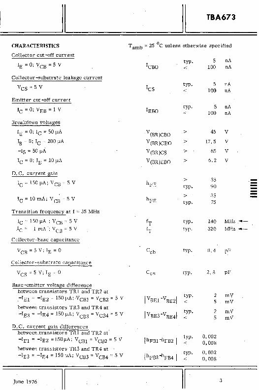
II II TBA673
CHARACTERISTICS Tamt, = 25 °c unless otherwise specified
Collector cut -off current typo 5 nA
IE = 0; V CB = 5 V ICBO < 100 nA
Collector -substrate leakage current
Ves = 5 V ICS typo 5 nA < 100 nA
Emitter cut -off current
IC = 0; V EB = 1 V lEBO typo 5 nA < 100 nA
Breakdown voltages
IE = 0; IC = 50 fJA V(BR)CBO > 45 V
IB = 0; IC = 200 fJA V(BR)CEO > 17,5 V
-IS = 50 fJA V(BR)CS > 65 V
IC = 0; IE = 10 fJA V(BR)EBO > 6,2 V
Do Co current gain
IC = 150 IJA; V CB = 5 V hPE > 35 typo 90
> 35 -IC = 10 rnA; V CB = 5 V hPE -typo 75
Transition frequency at f = 35 MHz
IC = 150 fJA ; V CB = 5 V fT typo 140 MHz .-4-
J C = 1 rnA ; VCB = 5 V fT typo 320 tvillz -4-
Collector-base capacitance
VCB =5V;IE =0 Ccb typo 0,4 pP
Collector-substrate capacitance
VCS =5V;IE =0 Ccs typo 2,8 pP
Base -emitter voltage difference between transistors TRI and TR2 at
2 mV .-IE1 = -IE2 = 150 fJ A; VCBl = VCB2 = 5 V I VBEl -VBE2! typo
< 5 mV between transistors TR3 and TR4 at
2 mV -IE3 = -IE4 = 150 fJ A ; VCB3 = VCB4 = 5 V IVBE3-VBE41
typo < 5 mV
DoC 0 current gain differences between,transistors TR1 and TR2 at
0,002 -lEI:;::; -IE2 = 150 f.1A ; VCB1 = VCB2 = 5 V I hpBl -hpB2 I typo
< 0,008 between transistors TR3 and TR4 at
0,002 -IE3 = -IE4 = 150 fJ A; VCB3 = VCB4 = 5 V I hPB3 -hpB4 I typo
< 0,008
June 1976 II II 3

------
TBA673
II APPLICATION INFORMATION
Telephony carriers ring modulator
Rj 6kn
3k.Cl.
3 kll
TBA673
2:(1+1) --
~ Performance at T amb = 25 °c Conversion gain at fa = 1 kHz
Vi = 0,4 V; fp = 34 kHz
Vcarrier 0.28 Vrms
Carrier leakage power in Ro at 1> = 34 kHz
4 II
5
+VB 1.5V
++VB 9V
7ZS5943
typo -0,75 dB
typo 3 nW
II April 1973

II II TBA915
AUDIO AMPLIFIER
The TBA915 is a monolithic integrated a. f. amplifier designed for use in small communication receivers, where low battery drain is of paramount importance. The output power of the device is 500 mW and the zero-signal current is only 2 rnA (typ.). The circuit can be squelched to a stand-by current of 0,4 rnA.
April 1973
II
5.1 nom 9.4 max
QUICK REFERENCE DATA
-I~I_. ~12o:..:..!....7m_in_.1 7ZSSJ26
II

N
§ (!)
..... \0 "-l 0-.
Hf'rm:
CIRCUIT DIAGRAM
9 5-
r---~---'-----.----~------------------+-----~-----------------.---+---.--~----~--~~04
012 6
TR18
03 07
3
80 04
08
R10
09
~--~-----------+------~~--~--~-------------4--------~~----------~~02 7Z61,.570.1
10
-t ~ » --0 -U'I

II TBA915
RATINGS Limiting values in accordance with the Absolute Maximum System (IEC 134).
Voltages (pin 2 must be externally connected to pin 10)
Pin No.4 voltage
Pin No.8 voltage
Pin No.3 voltage
Currents
Pin No.4 current
Pin No.3 current
,Pin No.7, current
Pin No.8 current
Pin No.5 current
Pin No.9 current
Pin No.1 current
Total power dissipation
1000
Ptot (mW)
500
o -100
Temperatures
Storage temperature
Operating ambient temperature see derating curve above
April 1973 II
~ I'-,
I\.. I\..
a
V 4-2 max. 17 V
±V8-7 max. 5 V
V3-2 max. 17 V
14 max. 350 rnA
±I 3 max. 350 rnA
17 max. 0,5 rnA
18 max. 0,5 rnA
IS max. 5 rnA
19 max. 5 rnA
{ +11 max. 1 rnA
- II max. 10 J.lA
7Z67343
"-
" " " I'-
100 'T amb (OC) 200
T stg -55 to +125
Tamb' -55 to +125
II 3
---= -

TBA915
II I ,
CHARACTERISTICS at T amb = 25 oC; V p = 12 V
Measured in the test circuit below
Output power at dtot = 5% Po typo 500 mW
Bandwidth (-3 dB) B > 6 kHz
TotaL current (d.c.)
no signal Itot typo 2 rnA
.....--. < 3,7 rnA
no signal with squelch Itot typo 0,4 rnA
with signal at P 0= 500 mW Itot typo 72 rnA
Total distortion at Po = 500 mW dtot typo 2,5 %
'< 5 %
Input signal at Po ::;:,500 mW Vi typo 10 mV < 15 mV
Input impedance IZd typo 9 kQ
Signal-to-noise ratio - related to'Po = 500 mW -- S - RS = 600 Q; B = 300 Hz to 6 kHz typo 72 dB - N -. Bias current 19 > 25 llA
Test circuit squelch
+12V
125~F
20.n
~ SQUELCH REQUIREMENTS at 19 = 25 ~
{ VI > 800 mV
II > 10 IJA Squelch "on"
Squelch "off" VI < 400 ' mV
4 II II June 1976

Ii II TCA210
AUDIO AMPLIFIER AND PRE-AMPLIFIER
The TCA210 isa monolithic integrated circuit comprising two amplifiers for use in intercoms and other audio systems. The first is a high-gain pre-amplifier with differential input and I;l c1ass-A output stage which can deliver 2,5 mW into an 800 Q load. The second is a power amplifier with a c1ass-B output stage capable of deHvering 500 mW into a 25 Q load. Speech rating: up to 800 mW can be delivered into a 15 Q load for short periods. When there is no signal, the current consumption is 8 rnA (typ.). Squelch provision incorporated in both amplifiers can be used to ensure maximum battery life.
QUICK REFERENCE DATA
Supply voltage Vp nom. 12 V
Total current drain Itot typo 8 rnA
Pre -amplifier
Open loop voltage gain Gv typo 10000
Output power at R L = 800 Q Po typo 2,5 mW
t\oise figure (B = 300 to 4000 Hz) RS = 500 Q F < 6 dB
Unity-gain bandwidth (compensated) B > 10 MHz
Output amplifier
Open loop voltage gain Gv typo 500
Output pow.er at RL = 25 Q; dtot = 5% Po typo 500 mW at R L = 15 Q; dtot = 5% Po typo 800 mW
PACKAGE OUTLINE plastic 16-lead dual in-line (see general section).
August 1976 II 1
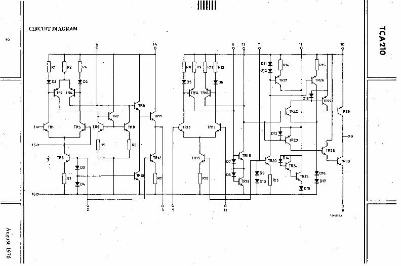
~
)s:: ~ ~ ...... \0 -...] ()\
1111111
-CIRCUIT DIAGRAM
4 14 12 11
150 ~
J~-L~'~I~~~~~~ 160-
13
10
.... n » ~ -.. o

II II TCA210
RATINGS Limiting values in accordance with the Absolute Maximum System (IEe 134)
Voltages; pin 8 must be externally connected to pin 16
Pins 3, 9, 10, 14 with respect to pin 16
Pins 1, 15, 5, 13 with respect to pin 16
Pin 1 with respect to pin 15
Pin 5 with respect to pin 13
Currents
Pin 10
Pin 9
Pin 8
Pin 14
Pin 3
Pins 2, 4, 6, 7, 11, 12
Pins 1, 15, 5, 13
Total power dissipation
1000
Ptot (mW)
500
1\
\ , 1\ ,
\ , 1\
o -100
Temperatures
Storage temperature
o
Operating ambient temperature (see also graph)
, \ ,
100
max. 17 V
max. 17 V 1)
max. ±5 V
max. ±5 V
max. 550 rnA
max. ±550 rnA
max. 550 rnA
max. 20 rnA
max. ±20 rnA
max. 5 rllA.
max. 0,5 rnA
7Z622941
1\
\
T stg -55 to + 125 °c Tamb -55 to +125 °c
1) FGF a supply voltage less than 14 V, the maximum input voltage is equal to the supply vQltage.
August 1976 II II 3
--

lCA210
II II CHARACTERISTICSatTamb = 25 °C; Vp = 12 V
Input bias current; pins 1 and 15 ! (II + 115) typo 2,5 IlA
Total current; pin 14 114 typo 4 rnA
Bias current; pin 2 12 typo 200 IlA
Input current; pins 5 and 13 ! (IS +113) typo 2 IlA
Total current; d. C. ; no signal; pin 10 110 typo 4 rnA
Bias current; pin 7 17 typo 150 IlA
Pre-amplifier
Open. loop voltage gain Gv > 65 dB typ, 80 dB
Noise figure at RS = 5 kQ; B = 300 to 4000 Hz F typo 4 dB
Current in the output transistor IC > 2,5 rnA Unity gain bandwidth with 6 dB/oct compensation B typo 10 MHz
Output amplifier
Open loop voltage gain Gv typo 54 dB
Total distortion at f = 1kHz; Po = 50 mW; RL = 25Q ~ot typo 1,5 %
Maximum output power at dtcit= 5%; RL = 25Q Po typo 450 mW
4 II II August 1976

II II TCA210
APPLICATION INFORMATION
Pre-amplifier and output amplifier for intercom systems
,--...,.-------+--....,....-----.--_---------'-O+12V
Performance T amb = 25 °C; V P = 12 V --Pre-amplifier --Output pgwer at RL1 = 800 Q Po typo 2,5 mW -Bandwidth (-3 dB) B typo 4 -kHz Total current 114 typo 4,0 rnA Input signal ViI typo 1,5 mV Input impedance IZii typo 500 Q
Output amplifier
Output power at RL2 = 25 Q; dtot = 5% Po typo 500 mW at RL2 = 15 Q; ~ot = 5% Po typo 800 mW
Bandwidth (-3 dB) B typo 4 kHz Total distortion at Po = 50 mW dtot typo 1,5 % Input signal Vi2 typo 260 mV Input impedance IZil typo 1,3 kQ Total current (d. C. ; no signal; pin 10) 110 typo 4 rnA
August 1976 II 5


Ii II TCA240
DOUBLE BALANCED MODULATOR/DEMODULATOR
The TCA240 is a monolithic integrated circuit used ,for general 'purpose applications, such as:
- modulator
- mixer
- switch/chopper
- a.m. synchronous demodulator
- f.m. quadrature demodulator
- phase comparator
- differential amplifier
The circuit is arrange~ to offer very flexible circuit design possibilities. The excellent matching and temperature tracking of the transistors in the circuit allows the use of circuit techniques which are not available when using discrete devices.
PACKAGE OUTLINE plastic 16-lead dual in-line (see general section).
August 1976 11 II 1
----

TCA240
II II CIRCUIT DIAGRAM
14 12 4 5 13 11
3 6
20-----f 1-----07
+------08
150--"'---f 1---..---010
160---""---' +----4---0 9
--Note
Pins 16 and 9 are connected to the substrate. When both long tailed pairs are used connect pin 9 with pin 16 externally.
RATINGS Limiting values in accordance with the Absolute Maximum System (IEC 134)
Voltages (each transistor)
Collector-substrate voltage (open base and emitter) VCSO max. 16 V
Collector- base voltage (open emitter) VCBO max. 16 V
Collector-emitter voltage (open base) VCEO max. 12 V
Emitter-base voltage (open collector) VEBO max. 5 V
Currents (each transistor)
Emitter current IE max. 10 rnA
Base current IB max. 10 rnA
2 November 1974

II II TCA240
RA TlNGS (continued)
Total power dissipation (mounted on a printed-wiring board)
1000
Ptot (mW)
500
o o
Temperatures
Storage temperature
.......... ........
Operating ambient temperature
Crystal temperature
THERMAL RESISTANCE
From crystal to ambient
May 1974 II
,.... ...... .... ~
i""oool ...
r,
50
, 7268974
~ r,i"oo,
.... ~
100 Tamb (oC) 150
T stg -55to+125 °c
Tamb -20 to +70 °c Tc max. 125 °c
Rth j-a 200 °C/W
3
--

--
TCA240
II II CHARACTERISTICS at V 11-9 = V 13-9 = V 12-16 = V 14-16 = 12 V;
V3-16 = V4-16 = V5-9 = V6-9 = 6 V;V2-16 = V7-9 = 4 V; T amb = 25 OC; unless otherwise specified
Collector current difference
between transistors TR4 and TRS I 10 = I 15 = 1, 5 rnA IIC4 - IC81 < 0,07
Base-emitter voltage
Of transistors TRa and TR 7 Il=I8=-lrnA VBE3;VBE7 690 to 770
Base-emitter voltage difference
between transistors TRI and TR2 V12-16 = V14-16 = 10 V;Ii5 = 1,5 rnA between transistors TR5 and TR6
IVBEI- VBE21 .,-:: 2,5
Vll-9 = V13-9 = 10 V;I1O =·1,5 rnA IVBE5 - Vr3E6 I < 2,5
between the parallel connection of TRl, TR5andTR2, TR6 Vll-9 = V13-9 = V12-16 = V14-16 = S V
I V BE 1; 5 - V BE2 ; 61 Il+ 1S=-3rnA < 2,1
D. C. current gain
of transistors TR3 and TR 7 11+ I S=-3rnA hFE3,hFE7 2:3 to 190
D.C. current gain ratio
of transistors TR,) and TR 7 I hpE3 - hFE71 11+1S = -3 rnA x200 o to 60 hpE3+ hFE7
D. C. current gain
of transistors TR 1 ,'TR2, TR5 and TR6 IE, = 750 .f1A hFE 1, hFE2, hFE5, hFE6 2:3 to 190
D. C. current gain ratio
of transistors TR 1 and TR2 /hFEl-hFE21 11=-1,5mA x200 o to 60 hFE 1 + hFE2
of transistors TR5 and TR6 I hFE5 - hFE61 IS = -1,5 rnA x200 o to 60 hFE5+ hFE6
rnA
mV
mV
mV
mV
?(I
(f1 10
%
4 ' I II May 1974

II CHARACfERISTICS (continued)
D. C. current gain
of the paralleLconnection of TRI and TR6 at II + 18 = -3 rnA
of the parallel connection of TR2 and TRS at II + 18 = -3 rnA
D. C. current gain ratio
of the parallel connection of TR 1, TR6 and TR2, TRS II + 18 = -3 mA
DYNAMIC DESIGN DATA
Noise figure at f = 100 MHz
I
hFE1 ;6- hFE2;SI x200 hFE 1; 6+ hFE2; 5
IC = 1 mA;VCB = 5 V;Gs = 3,7 mA/V;Bs = -2,5 rnA/V IE = 2, 5 rnA; V C B = 5 V; G s = 6, 5 rnA /V ; Bs = - 2 ,SmA /V
F F
y parameters
II
<
<
VCE = 5 V;f = 100 MHz
Input conductance
IE = 1 rnA
Input susceptance Feedback admittance Phase angle of feedback admittance Transfer admittance Phase angle of feedback admittance Output conductance Output susceptance
Frequency response (see circuit on page 6)
IS = 5 mA;RC = 600 Q;f = -3 dB
Switching times (see circuit on page 7)
Rise time Fall time Rise propagation delay time 1) Fall propagation delay time 1)
1) Reference level 50 %.
November 1974 II
gie bie IYrel
-'Pre IYfe I
--ffe goe boe
IS
tr typo tf typo tpdr typo tpdf typo
typo 4,4 typo 7,6 typo 0,4 typo 100° typo 22 typo 45° typo 0,4 typo 1,8
typo
0,5 1
2,9 2,7 1,4 1, .'3 1, 1 1,2 1, 1 1,2
II
TCA240
2:3 to 190
2:3 to 190
o to 60 %
3,7 dB 4,2 dB
IE = 5 rnA
13,6 rnA (V 9 mA/V
0,4 mA/V 100° 55 mA/V 96 0
0,5 mA/V 1,8 mA/V
34 MHz
2 4 rnA
2,7 3,1 ns 1,6 2,3 ns 1,4 1,7 ns 1,4 1, 7 ns
5
--

-.., =
I
TCA240
II DYNAMIC DESIGN DATA (continued)
10V VS2
100 1,5
100 1,5 nFl ~nF
nF~ lnF ~---------+---+ Vo
6,8kfl 5,6kn
5;6kn
16 7Z6t.783
L. _______ .J
Circuit for measuring the frequency response
6 II II May 1974

II II TCA240
DYNAMIC DESIGN DATA (continued)
~----+---~------~---1------------~--~--~--1
~+---~--+-------+---~
1nF
'- _______ .J
Circuit for measuring tp tf' tpdr and tpdf
May 1974 II
100 . nF
7

)

II II TCA580
INTEGRATED GYRATOR CIRCUIT
The TCA580 is a monolithic integrated gyrator Circuit with floating inputs. It is intended mainly to replace the coils in telephony low-pass filters. The simulated inductance consists of the IG, two resistors Rg1 and Rg2 and a capaCitor C2. With this configuration, inductances of up to 1 MH ± 2% can be achieved.
QUICK REFERENCE DATA
Supply voltages Vp typo 4,4 V V N typo 7,6 V
Supply current Ip typo 0,8 rnA
'Frequency range f d.c. to 10 kHz
Quality factor at f = 200 Hz Q 500 to 5000
Efficiency r) typo 1,4 %
Operating ambient temperature Tamb -20 to +70 °c
BASIC CIRCUIT
9
6 P' 5
1
9;
~ J C2 -
1Z74279
PACKAGE OUTLINE plastic 16-lead dual in-line (see general section).
August 1976 II II 1
----

TCA580
II II CIRCUIT DIAGRAM
Cl
---' .. --
C2
2
II II April 1976

II II TCA580
SIMPLIFIED CIRCUIT DIAGRAM
C1 C2
7Z74281
RATINGS Limiting values in accordance with the Absolute Maximum System (lEC 134)
Voltages
Supply voltages Vp to VN max. 14 V
Common mode input voltage ±VIC max. 14 V
Differential input voltage ±VIO max. 11: V
Temperatures
Storage temperature T stg -55 to +125 °c Operating ambient temperature Tamb -20 to +70 °c
April 1976 II II 3

= --
TCA580
II II CHARACTERISTICS at Vp = 4,4 V; VN = 7,6 V; Tamb == 25 °c Supply current (adjust with Rp = 50 kQ) Ip typo '0,8 rnA
Efficiency: signal power supply power n typo 1,4 %
Tolerance of inductance ~L ~ ±0,2 % Quklity factor at f = 200 Hz;
Rgl = Rg2 = 10 kQ; pin 11 earthed Q 500 to 5000
Output voltage (peak value) Vom < 1,6 V
Input offset voltage Vio < 25 mV
Input offset current Iio < 9 fJA
Vp
~~nF "'" :11' L 11
:f
The values for Land fres in the circuit above are:
L =RgIRg2 C2 = 8,2 H
4
---;:========= == 194 Hz 27r V Rgl Rg2 Cl C2
II II April 1976

2500
Q
2000
1500
1000 10
11
If , v:
~ i"""" -
II , I I ,
I I I
I I
I I
I I
I ,
f res (Hz)
Quality factor as a function of frequency at pin 11 connected to earth.
April 1976
II II
TCA580
1Z14283
----
5

----
TCASSO 'II II Circuit and response of a low-pass filter with three TCA580 gyrators.
0,2
(dB)
0,1
o
1 -0, 2 10
6
pass-band
~ """ .-V ""'"
I
I '1 A I
attenuation - "
7Z74282
10kn ± 1 %
7Z74284 60
l" II "' (dB)
band ~ IU 1\ 40
r 20
/'-/
............ 11 o
f (Hz)
II April 1976

II
I.F. LIMITER-AMPLIFIER with very low current consumption
TCA770 TCA770A TCA770D
The TCA 770 is a limiter-amplifier with a balanced f. m. detector and an audio preamplifier intended for a frequency range of 100 kHz to 500 kHz with narrow band f. m. The circuit is especially intended for use in portophone sets, where low current consumption and high sensitivity are important.
QUICK REFERENCE DATA
Supply voltage
Ambient temperature
Frequ.ency
Total current consumption
Input limiting voltage (-3 dB)
A. F. output voltage at .6.f =' ± 3, 5 kHz (r. m. s. value)
A.M. rejection at .6.f = ±3,5 kHz;m = 0,3;fm = 1kHz Vi = 1 mV
Open loop voltage gain
PACKAGE OUTLINES (see general section).
TCA770 : SOT-43 (plastic; 14-lead). TCA 770A: plastic 16-lead dual in-line. TCA 770D : SO -14 (plastic 14-1ead flat pack).
July 1976 II
Vp
Tamb
fo
Itot
Vi lim
V o(rms)
a
Gv
II
typo 7,5 V
typo 25 °c typo 100 kHz
typo 450 ~
typo 30 jJV
typo 90 mV
typo 50 dB
typo 600
---
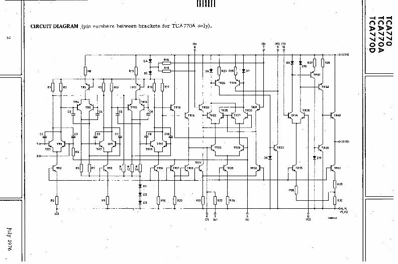
N
'-< s:: -< I-
'" -...J Q\
- --lTnrrr
CIRCUIT DIAGRAM ,(pin numbers between brackets for TeA 770A only),
(91 8
(81 7
(10) (11) 9 10
04 R18 09 R27n OR28
)R6 RI3~. 05 H ~ 06 [)R23 R25 ). 07 010 ~R37
"I 0" "~,, 1 J., '''P-J '''1 I)., M~ =~ ~-("" o n;;-k¢> -k"" -{mID -
"L='-:~' ! 1'~~i' ,,"" ~*Jl m~J'k-t---+---, >-- - --
C1r --::.... C3 F'-'- C7 J.,C9" - Cl0
J( TR~ -~ TR~ J) TR1!; !~ ~ ~ TR'V' II]R4 I TR7 Y TR1V TR23 TR2(' ~TR33 KTR39
'" "I i)"~,, f, 11 r, ] r.] rio. ~ .. ~ ~m" '''11"' I'm. '" 1"'" " ;[ 1 .,
"1 ~Il :: n·"· I'." ",1] -J.n I)'" '" ~ " CJ I
6 3 (7) (41
5 (6)
11 (12)
13(15)
12(13)
4,14 5,16)
~~~ nnn l>l>l> """""" ,,'~"" 000 '0 »

II TCA770 TCA770A TCA770D
RATINGS Limiting values in accordance with the Absolute Maximum System (IEC 134)
Supply voltage (pin 13 or 15)
Storage temperature
Operating ambient temperature
Vp
T stg
Tamb
max. 15 V
-55 to +125 °c -30 to +70 °c
CHARACTERISTICS at Vp = 7,5 V; T amb = 25 oC; fo = 100 kHz; measured in circuit on page 4. The pin numbers between brackets for TCA770A only.
Total current consumption
Supply voltage range
Power dissipation
I.F.lirniter-amplifier and f.m. detector
Input limiting voltage (-3 dB)
A. M. rejection f. m. signal: ~f = ±3, 5 kHz; fm = 70 Hz a. m: signal: .. = 0,3; fm = 1 kHz
at Vi = 300 llV atVi= 1mV at Vi = 10 mV
Input impedance; pin 1
A. F. output voltage; pin 9 (10) load == 100 kQ; ~f = ±3, 5 kHz; fm = 1 kHz; Vi = 10 mV (r.m.s. value)
Influence of ambient temperature on output voltage
Distortion at ~f = ±5 kHz; fm = 1 kHz
A.F. amplifier 3)
Open loop voltage gain (R load = 00)
Input bias current; pins 10 and 11 (11 and 12)
Current of current sink in output stage
1) See also left-hand graph on page 4.
2) See also right-hand graph on page 4.
V 13-14
Vi lim
0'
0'
0'
typo 450!lA 300 to 600 !lA
5 to 10 V
typo 3,4 mW 2,5t04,5 mW
typo
typo typo typo
>
40 dB 50 dB 60 dB
10 kQ
Vo(rms) typo 90 mV
typo
typo <
typo
typo
typo
6,2
2 3
600
dB/lOa 0C 2)
% %
270 nA
56 !lA
3) If the a. f. amplifier is not used, pin 11 (12) must be connected to Vp.
July 1976 II II 3

---
TCA770 TCA770A TCA770D
40
30 \ \ \ \typ
\ \.
20
I
\.
10
o 100
\ i\. ,
200
7Z&4830
/ ......,.~
2,5
Vo (dB)
o
-2,5
-5
-7.5 400 800 -50
f(kHz)
I
"'" ~
~
"- typ "I ,
'\
o
TEST CIRCUIT (pin numbers between brackets for TeA 770A only).
7Z648311
~
j ~ )
._-t- t-
lte
r----...---vp 13 (15) r--------------------- -,
I
I.F. AMPlIFIER/ DETECTOR
>-~~-+--+ V **) (RL~10kn)
3 (4i 7 (8)- 5 (6)- 6 (7)- 8 (9)-
120 120 pF pF
2,2nF
1,1mH
Q=2,5
5,6kfi
100kn gain
adjustment
1nF~.. ~11.lF ~ ~ 7Z64832.3
>:C) The input limiting voltage depends on capacitor values. (Suggested type: solid aluminium capacitor,. 2222. 122 56687; 0, 68 ~ /25 V).
**) Vo = (R1 + R2)/RZ x Vll-4. '
4 II II J~ly 1976
I ~

II II TCA980
MICROPHONE AMPLIFIER
The TCA980 is a monolithic integrated microphone amplifier. It is. primarily intended for use with low-impedance microphones in telephone systems. The output of the amplifier is 22 mV /~ar when used with a microphone haVing an impedance of 200 Q and a sensitivity of 100 !-IV /~r. A capsule assembly containing the TCA980, a low-impedance microphone and aQ, 22 ~ capacitor can directly replace a carbon microphone. The d. c. supply to the device may be of either polarity.
QUICK REFERENCE DATA.
Supply Cl,lrrent
Supply voltage drop at ± 12 = 10 rnA
Voltage gain at ± I2 = 30 rnA at±I2=lOrnA
Output impedance at ± 12 = 30 rnA
PACKAGE OUTLlN~
TO -12 (reduced height)
n~ 8,5
max
1
± 12 10 to 100 rnA
±VI-2 typo 4,5 V
Gv typo 220 Gv < 260
IZol typo 150 Q
Dimensions in mm
.----'0,48 +max
..... 14,67 max 1-12,7 min -
-9,4mdx-7Z69267
October 1974 II II 1
------

::> ;
r ~
o .J :..
CIRCUIT DIAGRAM
R5 ~,2kn
IIlIur '
I , I 02
':I
R11 42n
• " 04
7Z64880.1
I
-I . n • -o,~ . 01)
o

II TCA980
RATINGS Limiting values in accordance with the Absolute Maximum System (lEC 134)
Currents
Supply current (d. c.)
Non -repetitive peak current
Current into pin 3 (d. c.)
Power dissipation
Total power dissipation
Temperatures
Storage temperature
Ambient temperature
Crystal temperature
THERMAL RESISTANCE
From crystal to case
From crystal to ambient
October 1974
750
Ptot (mW)
500
250
o
II
-50
±IZ max. 100 rnA
100 rnA (a. c.) superimposed on 100 rnA (d. c.)
+13 max. 100 [lA
See derating curve below
T stg -55 to + lZ5 °c
Tamb -55 to + lZ5 °c
Tcr max. lZ5 °c,
Rth cr-c 65 °C/W
Rth cr-a 180 °C/W
7Z64879
r\. \ ~ , \
f\. ~ \ ~-f-~ ':f {" <:). -I--
, ~\ \~~'-- "" r---
"Vo-r--' ~-
I,\~~~~ 1,\ ' ~
r\. \ ~ \
\..
o 50 T. (oC) 100 amb
II 3
------

------
TCA980
II II D.C. CHARACTERISTICS 1) at Tcase = 25 oC; measured in circuit below)
Supply voltage drop
±I2 = 10 rnA ±I2 ::; 30 rnA ±I2=60rnA
A.C. CHARACTERISTICS
Voltage gain (measured in circuit below)
f = 2 kHz; ±12 = 30 rnA
f =2 kHz;- ±I2 = 1.0 rnA
Change of voltage gain
when changing Tamb from -20 to + 55 oC
Gain red~ction
between f = 0, 3 and 2 kHz
Output voltage at f = 2 kHz; ~ot < 5% (r. m. S. value)
±I2 = 10 rnA ±12 = 30 rnA
±I2 = 60 rnA
Noise output voltage
B :::; 0,3 kHz to 4 kHz (r. m. s. value)
Output impedance
f = 2 kHz; ± 12 = 30 rnA
2
4 II
±Vl-2 ±Vl-2 ±V 1-2
Gv
Gv
~Gv
~Gv
V o(rms) V o(rms)
Vo(rms)
Vn(rms)
IZol
II
3,50 to 5,75 V 4,45to6,75 V 5, 00 to 7, 80 V
typo 220 190 to 260
160 to 260
< 10 %
typ, 1 dB < 3, dB
> 1 V > 1,35 V > 1 V typo 1,5 V
< 1,3 mV
typo 150 - Q
October 1974

II TDA1022
BUCKET BRIGADE DELAY LINE FOR ANALOGUE SIGNALS
The TDA 1022 is a MOS monolithic integrated circuit, . generally intended to delay analogue signals (e. g. delay time = 512/2 fef». It can be used with clock frequencies in the range 5 kHz to 500 kHz. The device contains 512 stages, so the input signal can be delayed from 51,2 ms to 0,512 ms. Applications in which the device can be used:
- variation of fixed delays of analogue signals, vox control, equalizing speech delay in public address systems;
- in electronic organs and other musical instruments for .vibrato and chorus effects; - reverberation e'ifects; - variable compression and expansion of speech in tape-recorders; - in communication systems for speech scrambling and time scale conversion.
QUICK REFERENCE OAT A
Supply voltage (pin 9) VDD nom. -15 V
Clock frequency fef> 5 to 500 kHz
Numb~r of stages 512
Signal delay range td 51,2;0 0,512 ms
Signal frequency range fs o (d.c.) to 45 kHz
Input voltage at pin 5 (peak-to-peak value) V 5-16(p-p) typo 7 VI
Line attenuation typo 4 dB 1)
PACKAGE OUTLINE· plastic 16-lead dual in -line (see general section).
1) See note 1 on page 4.
June 1976 II II 1
--

t>,)
0 n I"T 0 0-(I) t-j
t-\0 -.J UI
IIHIII
CIRCUIT DIAGRAM
13
123
50 lilT1±ln:±n±lT1tn±lT1± 1 .1 ~ .1 ~ ~ .i--, ~.l-=
r 4: 1" ---02
,1 --- 01
&16 512 514
----~±l I l±n±rr---l± r--'--~------------------~09
IT l}! ::~-r--:--_ 1 ------'
~T ou
11 08
7Z69739
PINNING
1. Clock input 1 (V CL1) ,5. Signal input 9. Negative supply (VDD) 13. Tetrode gate (V 13-16)
2. Not connected 6. Not connected 10. Not connected 14. Not connected
3. Not connected 7. Not connected 11. Not connected 15. Not connected
4. Clock input 2 (V CL2) 8. Output 513 12. Output 512 16. Ground (substrate)
..... c » -o ~ ~
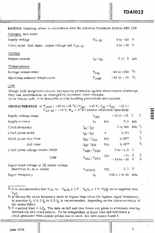
II II TDA1022
RATINGS Limiting values in accordance with the Absolute Maximum System (lEC 134)
Voltages (see note)
Supply voltage
Clock input, data input, output voltage and V 13-16
Current
Output current
Temperatures
Storage temperature
Operating ambient temperature
Note
V9-16
18; 112
T stg
Tamb
o to -20 V
o to -18 V
o to 5 rnA
-40 to +150 °c
-20 to + 85 °c
Though MOS integrated circuits incorporate protection against electrostatic discharge, they can nevertheless be damaged by accidental over-voltages. To be totally safe, it is desirable to take handling precautions into account.
CHARACTERISTICS at Tamb = -20 to +55 °C; VDD = -15 V; Vebi = Veb2 = -15 V; VI3-16 = -14 V; RL = 47 kQ (unless otherwise specified)
Supply voltage range VDD -iOto-iS V
Supply current 19 typo 0,3 rnA
Clock frequency febI; feb2 5 to 500 kHz
Clock pulse width tebI; teb2 :s 0,5T
Clock pulse rise time teblr; teb2r typo O,05T
fall time teblf; t¢2f typo O,05T
Clock pulse voltage levels; HIGH VebIH; Veb2H o to -1,5 V
LOW VeblL; Veb2L t>:P· -15 V
-10 to -18 V
Signal input voltage at 1% output voltage distortion (r. m. s. value) V s(rms) typo 2,5 V
Signal frequency fs o (d. c.) to 45 kHz
1) It is recommended that V 13-16 = Veb 1L + 1 V = Veb 2L + 1 V; VD~ more negative than
Veb L·. . 2) In theory the clJck frequency must be higher than twice the highest signal frequency;
1)
2)
3)
3)
3)
1) 1)
in practice fs :s 0,3 feb to 0,5 feb is recommended, depending on the characteristics of the output filter.
3) T = period time = l/feb. The data on fall and rise times are given to eliminate overlap between the two clock pulses. To be independent of these rise and fall times a clock generator with simple gating can be used. See also pages 5.and S.
June 1976 II II 3
--

--
TOA1022
II II CHARACTERISTICS (continued)
Attenuation from input to output typo 4 dB
f4>:::: 40 kHz; fs = 1 kHz < 7 dB
Change in output at fs = 1 kHz; V s(rms) :::: 1 V typo 0,5 dB when f4> varies from 5 to 100 kHz
< 1 dB
when f4> varies from 100 to 300 kHz typo 0,5 dB < 1 dB
D. C. voltage shift when f4> varies from 5 to 300 kHz < 0,5 V
Noise output voltC\.ge (r. m. S. value) f4>:: 100 kHz (weighted by "A" curve) VN(rnis) typo 0,25 mV
Signal-to.-noise ratio at max. output voltage SjN typo 74 dB
RL > 10 kQ
Load resistance 47 kQ typo
1) Attenuation can be reduced to typo 2,5 dB if load resistor is replaced by a current source of 100 to 400 flA.
1)
1)
4 II October 1975

o ~ II TIMING DIAGRAM g. (l) ~
...... \.0 -...] VI
VI
OV t V"1H t 1,5 V max
\ / \90% 90%1- t V1*1
1211 INPUT +
V13- 16 \ I 110% 10% t • V01L I 6 V ~ 1V lUI
t I.. t01 .1 --I t01f 1-.-
OV • VI/l2H t I \ 1,5 Vmax I \ t
V2*1
1212 INPUT +
V13- 16 I \ I \ • V"2L r \ I \ 6 V ~ 1'J**1
t I. tl/l2 -I
I.. T .1 7Z69713
>!<) IV 1 + V 21 :::IV</>lL' ; V</>lL = V</>2L'
':<>:<) For maximum dynamic range adjust V13- 16 so that /:1V = V13- 16 - VrbL ~ 1 V.
1111111
..... C l> -o ~ ....:»

0-
o o M-g. (I) I-! .\0 '-l CI1
1111lU
APPLICATION INFORMATION
audio input -II I I 13 9 8 h-f H Vslrms)<2,5V 5 TDA1022 12U • 120kfi
16 1 4 , ,
RL= :Ie:le:le)
47kn
15V
56kn
4 J' U2 72kn 3 IJA741CV
7
61 output
210pF 56kO
~------~--+---~-+--------~----------~------+-~-------OV
.., n r!Zl2 L...J L...J U)
L-_r-- JlJl.. !ZI, 7Z69737
Single delay line connection
>:') Adjust d. c. voltage for class-A operation (:::: 5 V).
Conditions: low pass filter ~741CV(12 dB per octave); gain =+3,5 dB (compensation for line attenuation); fel> = 50 kHz (min.); cut-off frequency = 15 kHz:
* >:<) Clock input voltage amplitude: V C L = -15 V.
* * *) Can be replaced bya current source of 100 to 400 ~ (see also note 1 on page 4).
.... c » -o -~ ~
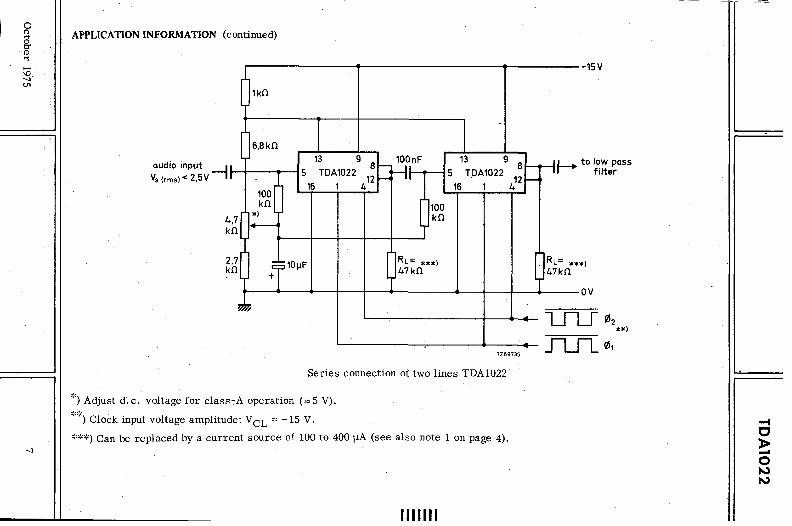
o g II APPLICATION INFORMATION (continued) g. rtl I-S
:a II -15V -..:t CJ1
--.]
audio input -I ..... -+--....... --1 Vs (rmsl < 2,5V
100nF
RL= ***1 47kO
13 9 5 TDA1022 8
16 . 412 i ,
L...... to low pass ~ filter
RL= ***1 47kO
~--~--~~~---+---+--------~--4---4---~-----OV
-, n r O2
LJ LJ **1
7Z69736 JLfi 01
Series connection of two lines TDA1022
':') Adjust d. c. voltage for class -A operation (:::: 5 V).
,:,>:') Clock input voltage amplitude: V CL =" -15 V.
':<>:<>:') Can be replaced by a current source of 100 to 400 flA (see also note 1 on page 4).
1111111
.... c » -o ~ ~

00
'2" g ...... \0
" '"
APPLICATION INFORMATION (continued)
(.
VDD = 0 -VSS = -15 V
112 HEF4011
4
IJUrlt
-15V- -15V
112 HEF4011
0 1
O2
w· .. ~ 7Z73980
-15V
feb_ = 15 kHz Glock oscillator and driver circuit with elimination 6f overlap (for max. 6 :iC. TDA1022)
-t C » -o ~ ~

15
Vo (V)
10
5
2
Vo(rms)
(V)
1,5
l-l-.....
.....
0,5 -5
~ ....-::::;V/
V V
V
October 1975,
k::: ~ V ,/
L
I
II "
TDAI022
1Z69735
typical values
V0L= -15V 14V
-bv AVV
~ -12V A /'
~ /' /' I /' -10V
,/
/' ,/
-5 -10 ..,15 Vs (V)
Conditions for the graph above: 7Z69732 VDD = -15 V
V13-16 = -14 V VcJ>H = 0 V
J
1/
if J
ty~/
, J ,
" /
-10 V(lJL(V)
1/
/
-15
fel> = 40 kHz RL = 47 kQ
Conditions for the left-hand graph: VDD = -15 V V13-16 = -14 V V<!>H = 0 V fcJ> == 40 kHz fs = 1 kHz RL = 47 k,~
9
-----

.0.-
::: ....
TDA1022
Vo Vs
(dB)
o
-2,5
-5
-7,5
-10
7,5
dtot (ota)
5
2,5
10
......... .........
""
7Z69731
typ
j LoI'"
Vs(rms) (V) 10
I
II 7Z69734
typical values
Vs=0,775 V
I"'" -..... ..........
~
" " " , '\. , ,
\
fl6=10 kHz 1--40 kHz_ -'.100 kHz I-
10 fs (kHz)
Conditions for the graph above: VOO = -15 V V13-16 = -14 V V<b = 0 to-IS V
Conditions for the left-hand graph: fs = 1 kHz Vs=-5,2V VOO= ...,15 V VI3-16=-14V V<b= 0 to -15 V fIb = 40 kHz
October 1975

GENERAL INDUSTRIAL
-----

/
--r
TYPE SELECTION
General industrial
SAA1927
SAK140
TCA280A
TDA0555D
TDAlOU·
II
- stepper motor driver
- revolution counter
- uniyersal triac control (trigger module)
- timer
- a mains-zero triac-triggering circuit
November 1976

II II
SAA1027
STEPPER MOTOR DRIVE CIRCUIT
The SAA1027 is intended for driving a four phase two stator stepper motor. The circuit consists of four output stage's, a logic part and three input stages. The logic part is driven by three input stages; a trigger input stage, an input stage which can change the switching sequence of the logic part so that the motor can rotate clock wise (CW) or counter clock wise (CCW) and a set input stage to set the four output stages. The three inputs are compatible with high noise immunity logic to ensure proper operation, even in noisy environments. The output can deliver 350 rnA in each phase. The right switching sequence of the four phases is obtained from the logic 'Part of the circuit. Integrated diodes protect the outputs against transient spikes.
QUICK REFERENCE DATA
Supply voltage Vp
Load current (each output) Iq max.
Logic for CW and CCW operation
PACKAGE OUTLINE '16 lead plastic power dual in-line (see page 9)
December 1974 II
9,5 to 18 V
350 rnA
1
---
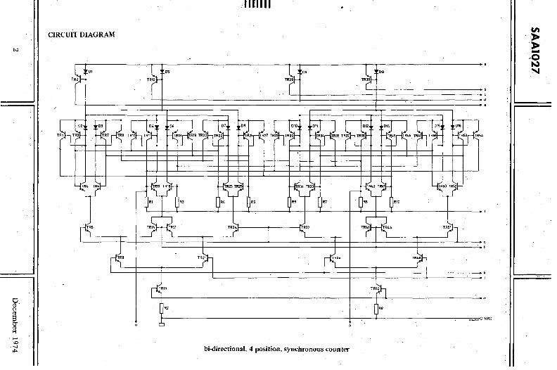
t-.J
~. (") (I)
3 0' (I) t-!
' ..... \0 "-I
*""
IIUIII
CIRCUIT DIAGRAM
01 'OS 09 013
TR2 TR12 TR29 TR39
Mt ~,t¢ ~~ ~~ '~f¢ ~~ ~, Rl TR3 ,~R7 TRB TR10 TR~ ~R1B TR19 TR20 TR=- ~26 TR27 TR28 TR=-- ~34 Trs TR37 TR=--, ~4S TR46 TR47 TR=-, ;53 TRS4
f-;-
I
TR4 TR6
r.YI ~7 M:7 M TRSO TR52
r-- ,.-
[ )Rl R3 R4 RS 1}6 [ t. IR10
rts ,~, TR;;;t 'lR32 ,~, T71 I 1 I
~ I ~ I
'~ ~ TR48
~" - TR~ r R2 R9
n"",22
bi-directional, 4 position, synchronous counter
S112}
en » » -·0 ~ 'I

tJ (l) ('l (l)
S 0" (l) 1-1 ..... \0 --.J ~.
CJ.)
017
018
Rll
025
019 026
supply voltages
trigger stage
CWjCCW stage
R32
set stage
d'
output stages
&It )I-)I--o ~ ........
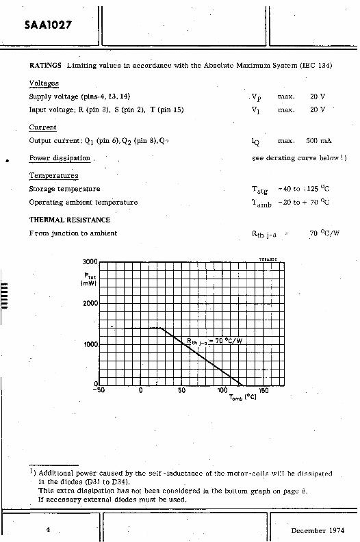
•
SAA1027
II II RATINGS Limiting values in accordance with the Absolute Maximum System (lEC 134)
Voltages
Supply voltage (pins·4, 13, 14)
Input voltage; R (pin 3), S (pin 2), T (pin 15)
Current ---Output current; Ql (pin 6), Q2 (pin 8), Q."
Power dissipation ,
Temperatures
Storage temperature
Operating ambient temperature
THERMAL RESISTANCE
From junction to ambient
3000
Ptot (mW)
2000
1000
o -SO
......
o
I" Rth j-a = 70 °C/W
""'~ "-
..... ro...
"'-" so
IQ
max.
max.
20 V
20 V
max. 500 rnA
see derating curve below 1)
Tstg -40 to +125 °c
Tamb -20 to + 70 0 C
Rth j-a 70 oC/W
7Z64952
1) Additional power caused by the self -inductance of the motor-coils will be dissipated in the diodes (D31 to D34). This extra dissipation has not been considered in the bottom graph on page 8. If necessary external diodes must be used.
4 I December 1974

II II SAA1027
FUNCfION TABLE
Direction conditions (R)
The direction of rotation can be changed at any moment independent of the state of the T and S inputs.
Set conditions (S)
When T is HIGH and S LOW then the outputs are set: Ql = L, Q2 = H, Q3 = L, Q4 = H.
Trigger conditions (T)
S=H
R=H
T Ql Q2 Q3 Q4 T Ql
0 L H L H 0 L 1 H L L H 1 L 2 H L H L 2 H 3 L H H L 3 H 4 L H L H 4 L
CHARACTERISTICS at Tamb = -20 to +65 °C; Vp = 12 V
Supply voltage (pin 14)
Sppply current (without load, all inputs HIGH, pin 4 open)
Input logic voltage levels and currents for R, Sand T HIGH
LOW
Supply voltage (each output stage)
Supply current (each output stage)
Saturation voltage of output transistors at IQ = 350 rnA (pins 6, 8, 9" 11)
Bias voltage and current (max. values; pin 4)
Bias resistor
Power dissipation in bias resistor
Total device power dissipation
December 1974 II
R=L
Q2 Q3 Q4
H L 'H H H L L H L L L H H L H
Vp typo 12 V
9,5 to 18 V
typo 4,5 rnA Ip
2,0 to 6,5 rnA
VIH > 7,5 V IIH typo 1 flA
VIL < 4,5 V
IlL typo 30 flA
VQ typo 12 V
1,5 to 18 V
IQ < 350 rnA
Vsat < 1,0 V
See top graph on page 7
See bottom graph on page 7
See top graph on page ,8
See bottom graph on page 8
II 5
-----

-F
SAA1027 . ·11
APPLICATION INFORMATION
Vp=12V Vs=12V
Is=80mAI Rs =120ntO,75W) 100n •
PINNING
1. not connected 2. S (set input) 3. R (CW /CCW input) 4. VB (positive supply)
81- DIRECTIONAL
4 POSITION
SYNCHRONOUS
COUNTER
5. Earth'(negative supply) 6. Q 1 (output) 7. not connected 8. Q2 (output)
6
V t. -12 Vo STEPPER MOTOR 4 13
... --Ia=350mAI
9 _13
OUTPUT Q3 1 STAGES a Q2 12 30n
t-"'+-~---t-..J
-I Ia=350mA 1
6 ~-- 1
9. Q3 (output) 10. not connected 11. Q4 (output) 12. Earth (negative supply) 13. VD (positive supply) 14. Vp (positive supply) 15. T (trigger input) 16. not connected
II
Va=12V 7Z64956
December 1974

600
I Q
(rnA)
400
200
o
20
VB (V)
15
10
5
II' 1/
o o
~ ~ ~ ~-
o 10
December 1974
II
, 1/
j
/
/' V ./ / ~
,...... --~ ~
II
SAA1027
7Z64953
IB V 4-12
j ~
/ ~
" ,
IL ~ L
~
'" r / ~
1 L V ,
/ l.I ,
..... ~
50
j
/ l/ ~
/
~ ~
,.~ I""'" ...... ~ ......
Ii
II
~
100
2
Id o-'o-L-t-4 S g ~
I ~ I J J
I I I I I L
1 1 I J 'I I I I
'I / I I / / I
V / / I / / /
V / j j
/ / / // / h
~ ./ /A~ ~ ..... ~ ~
.... ""1-' ~
150 IB (mA) 200
3
7Z64954
~o I 0 ~ ~Ln ~ U'I
II /I J /I
I I IJ /I I ~ II
J I Z I J
J 1/ "" II I I." IiI
1/ // II ~
-RB In)
II 7
--

-------
SAA1027
II 20
Va (V)
10
. l
II ~ J o Eo III 0
...... &n_ N '"
VI / fi I 1/
ff 1// I Iff/, V ) V
/1/ I / l'll l~ ~ ~(/
V
/ lV V
600
1a (mA)
400
I;' 10'
200 10'
~ LI
II
II
o J o 500
8 II
J
II
/ ~
~
I 7Z 55 649
0 g, ~ 0
~ Q Q N M -:t
V V / /
V ~V V
/ V
/ V V t:?"
/ V V V
-' V / ~ V
/
1,5
7269266
~ I,..Joiii'
t...."'" "'" 1,..1""
"'" ~ ,~~
I"
"""
1000 1500 2000 Ptot imW)
II December 1974
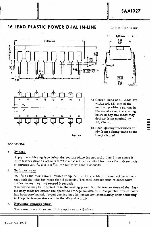
II II ~ SAA1027
16 LEAD PLASTIC POWER DUAL IN-LINE Dimensions in mm
I ...... ~------- 2',85malC--------
- 8,25max_6,48_
6,20
lj
:~!o 045 2,.6 '1x '... ~.IO,2541®1 Al
I ~ . .... 2,2 _1.--..l~_I_I_1.--1
max
I , I
" I II ~
t_~~
top view
SOLDERING
1. By hand
. , .... 1--__ 9,50 __ ---I .. 7,60 7Z55041."
A) Centre-lines of all leads are within ±O, 127 mm of the nominal positions shown; in the worst case, the spacing between any two leads may deviate from nominal by ±O, 254 mm.
B) Lead spacing tolerances apply from seating plane to the line indicated
Apply the soldering iron below the seating plane (or not mote than 2 mm above it). If its temperature is below 300 °c it must not be in contact for more than 10 seconds; if between 300 °c and 400 °C, for not more than 5 seconds.
2. By dip or wave
260 °c is the maximum allowable temperature of the solder; it must not be in contact with the joint for more than 5 seconds. The total contact time of successive solder waves must not exceed 5 seconds. The· device may be mounted up to the seating plane, but the temperature of the plastic body must not exceed the specified storage maximum. If the printed circuit board has been pre-heated, forced cooling may be necessary immediately after soldering to keep the temperature within the allowable limit.
3. Repairing soldered joints
The same precautions and liI!iits apply as in (1) above.
December 1974 II II 9
------


I II II SAK140
REVOLUTION COUNTER
The SAK140 is a monolithic integrated circuit intended for use as a revolution counter in motor cars. It contains a stabilization circuit and a monostable multivibrator which converts the circuit input pulses into output current pulses of constant duration and amplitude. This pulse duration is determined by an external R -C network; by proper choice of R and C, the circuit can be easily adapted to any milliammeter. Together with the internal stabilization circuitry this makes the indication almost independent of temperature changes and supply voltage variations ~
QUICK REFERENCE DATA
Supply voltage
Power dissipation at n = 6000 rpm; 10 = 12 rnA; Vp == 12 V
Input pulse amplitude (pin 1)
Output current (pin -9)
Vp 10 to 18 V
typo 130 mW
> 3,5 V
< SOmA
PACKAGE OUTLINE plastic 16-lead dual in-line (see general section).
August 1976 II II
--

tv
en .g 8 g. (1) 11 ~ \0
~
IUIIII
CIRCUIT DIAGRAM
120--~~----~~----~
05
01 013
.---+-------+---+---~--~----~--------~----~--~------_r----~----~---------+----~_+-----4~016
7 8 6 2 7Z64817
CIt » ~ -". o

II SAK140
RATINGS Limiting values)n accordance with the Absolute Maximum System (lEC 134)
Voltage
Supply voltage (pin 12)
Currents
Current at pin 9 (peak value)
at pin 7 (peak vahle)
at pin 8 (peak value)
at pin
Dissipation
Total power dissipatIon
Temperatures
Storage temperature
Ambient temperature
September 1974
750
Ptot (mWJ
500
250
II
........... i""o ......
!"' .... ........ """'"
25 50
Vp max. 18 V
-19M max. 50 rnA
-17M max. 50 rnA
-18M max. 50 rnA
±I1 max. 10 rnA
see derating curve below
....... "
Tstg
Tamb
.......
7Z14871
75 T. 10C) 100 amb
II
-40 to +80 °c "-40 to +80 °c
3
------
-----. -
SAK140
II II CHARACfERISTICS
Supply voltage range (pin 12) Vp 10 to 18 Vi).
Supply current (on-sfate) at Vp =: 12 V 112 typo SmA
Power dissipation at n = 6000 rpm;
10 = 12 rnA; Vp = 12 V Ptot typo 130mW
Voltage at pin 7 (on -state) V7-16 typo 2,5 V
Temperature coefficient
of output pulse (pin 9) typo 200 pprn/oC
Adjustable output current
resistor between pins 7 and 16 or 8 and 16 .< SOmA
Resistor for peak output current adjustment Rrn > 50 Q
Resistor for output pulse duration adjustment { typo 270 kQ R 0, 01 to 500 kQ
{ > 220 pF
CaEacitor for output pulse duration adjustment C typo 10 nF < 30 ~F
Input pulse frequency (for circuits on page 5) f < 400 Hz
Input pulse frequency (pin 2 not connected) f < 30 kHz
Influence of supply voltage on output amplitude
Vp from 10 to 16 V; top circuit on page 5 typo 0,6 % bottom circuit on page 5 typo 1,6 %
Input triggering voltage
at which level good triggering is achieved VI-16 > 3,5 V 2)
Duty cycle of output pulse IS typo 0,75 < 0;90
1) The circuit is internally protected against reverse connected supply voltage.
2) To prevent the input circuit from overloading by large input pulses a voltage r.egulator diode (DI3) has been connected at the input terminal. This diode also functions as a protection against negative trigger pulses. A resistor has to be connected in series with the input terminal, having such a value that the input current does not exceed 10 mAo
4 September 1974

II APPLICATION INFORMATION
SAK140
II 120n ~
Temperature coefficient of 10 is 800 ppm/oC determined by diode D. 1)
120n ~
15kn
2 3 4 5 6
SAK140
9
I
r----i I . I rI 10+
100nF=f= V27n
I I ~ Vp 7Z64878.t
SAK140
Temperature coefficient of 10 is 800 ppm/oC determined by an internal diode between pins 7 and 8. 1)
1) The influence of supply voltage variations is very small when using the top circuit. When using the bottom circuit the influence will be greater. The influence o,f the· temperature coefficients of R, C and Rm are in this case negligible.
September 1974 II II 5
--

----
SAK140
II II / Temperature coefficient of output current 10
c
SAK140
7Z64874
The temperature coefficient of 10 depends on the temperature coefficients of R, e, Rtn and the voltage, on pin 7. The temperatu're coefficient of R == 270 kQ (carbon resistor, catalogue number 2322 101 33274) is -330 ppm/oC and of V7 -16 is 200 ppm/oe. The temperature coefficients of Rm and e depend on the kind of components chosen. Their influence on the temperature coefficient of 10 are given below.
e = 10 nF Rm = 160 Q t. c. 10= 12 rnA
metallized polyester carbon resistor 440 ppm/oC capacitor (flat film type) t. c. = -220 ppm/oC t. c. = 350 ppm/OC catalogue number: catalogue number: 2322 101 33161 2222 342 25103
moulded metal film 190 ppm/oC resistor t. c. = 25 ppm/oC catalogue number: 2322 163 11601
tubular moulded carbon resistor -10 ppm/DC polystyrene capacitor t. c. = -220 ppm/DC t. c.= -100 ppm/oC catalogue number: catalogue number: 2322 101 33161 2222 435 21003
mOUlded, metal film -250 ppm/oC resistor t.c. = 25 ppm/DC catalogue number: 2322 163 11601
=~ In general: t. c. 10
6 II II September 1974

R (knl
II duty cycle = 1
--- duty cycle = 0,75 ~
1' .. "' ',- ~ ~" ~'Ioo. '" ',- ~ ~I" I",-~
'," ' " ~ ~. "'f' " '\ " r\. '\ I' ,C'~ , , , ... ~o ~ ~\ ~ '~" ~~ r'r. ~~ " ,,,", 1'" ~~ I· ~~ '~~~""' ' .. ~ -... ~.<- '\.. " '\ .' ': j, I"f' f' ',,, -,~:, <".<- f' ','\
, ~'" ~
, 1\ 1'1' I'~ " ~ ,~~ r, '~ " ~ 1', ~ ~.".<-1', ~ , ,
• .> .. ~ '- .... "- , '- ,".<-~ '- ~ ~ -.. " '~o".<-' ~ " ~ -" " , -, " I' ' .. " I' "-,
I'"
'" '" 1'-. I' ~ ... "' " , " ~ ~
1', '" ", '" 1'. I" ~~'" " ['\. r, " I\. I', '\. " ~.> , ,,- r'''.<-.... " '\ ['\. '\ " " '" ,,, 1', ~ , I'..
~ ',~.~~ f' I~ " ,'" 1', ['\~ r· r'~ " ,"-.. ~ ,~o' ~ ~
',~ ,?.<-,\ , I' ".'\ " ~: j, '" " " ,
'<~N ~ 1'1' ~'\" ~ 1\ hi' b\ ~".<- '. , ~" ~ -~~ r-,~ 1', ~l'!..
10 f (kHz)
SAK140
7Z64872
For other duty cycles at f. s. d. than '0,75, the value of R or C ~erived from the graph at a duty cycle of 1 must be. multiplied by the duty cycle required.
102 7Z64873
10
1 10
~~
" ~" ,~ " " ~" ,~ ~" ~
, I"""
'" r\ I'~
ro...
~' <,d., ~ 0,9 I
I"\: kO•75
. 0,6
'- '- '- [)\. ",0,504
" X .L" , " IX )o y O.3
"'''' I~~ >(O'~,l 1'\."-~ [Y ~ ."\. K> [)< I'\. ~r"\
1'1'\, "'\ ~ ~ ~ ~~ 1" ~
"< '\
" 1\ ['\1' ~I'
~ ~I' r--." ~ ~ I' " 104.
If a diode is connected in series with Rm' the value of Rm derived from the graph must be lowered with 25 %.
September 1974 II II 7
--


II TCA280A
TRIGGER MODULE
The TCA280A is a monolithic integrated circuit designed for thyristor and triac control. It contains the following circuit sections:
- d.c. power supply (intended for direct a. c. supply)
- zero-crossing detector (for synchronization of the trigger circuit)
- difference amplifier (used as a sensing amplifier)
- ramp function generator (operating as the sawtooth oscillator in time,..proportional control)
- output amplifier (amplifying the trigger pulses and feeding the thyristor or triac gate)
Various control modes possible when using the TCA280Aare:
- phase control
- synchronous on/off switching (static switch)
- time proportional control
The device is designed to be supplied directly from the a. c. mains through a dropping resistor, alternatively, supply can be obtained from a 14,5 V (d. c.) source connected between pins 11 and 16. The output current capability permits triggering of large thyristors and triacs.
PACKAGE OUTLINE plastic 16-1ead dual in-line (see general section.
August 1976 II II
---'-

N
>d
2: ..... \0 '-J ~
CIRCUIT DIAGRAM
13 r il-------l .1, I ~J i 02
03
04
01
L, _______ _ 16
nc. SUPPLY
1111111
1,---------------, I I
I 08 09
I
06
-------'1--
ZERO-CROSSING DETECTOR DIFFERENCE AMPLIFIER
,----------,
1 I
'10
020
RAMP FUNCTION GENERATOR OUTPUT AMPLIFIER
..... n » ~ CD o »

II TCA280A
RATINGS Limiting values in accordance with the Absolute Maximum System (lEC 134)
I Voltages
Currents
Total power dissipation
Temperatures
Storage temperature
1000
Ptot (mW)
500
a a
Operating ambient temperature
1) t::; 10 IJS
2) t :5 300 IJS
April 1974 II
V 11-16 V 11-7 Vl1-4 V S-16 VS-11 V9-16 V5-16 V 6-16
±V5-6 V 15-16
±113(AV) ±113M ±113SM -l lO(AV) -110M ±11M 12
±I3 15;16
-IS; -19 112 115
"
50
T stg Tamb
'" '" '"
max. 17 max. 17 max. 17 max. 17 max. 17 max. 17 max. 17 max. 17 max. 7 max. 17
max 30 max. 80 max. 2 max. 30 max. 600 max. 10 max. 200 max. 10 max. 10 max. 10 max. 10 max. 10
7Z70221
~
"-~
" ,
-55 to +125 -20 to +SO
11
V V V V V V V V V V
rnA rnA A 1) rnA rnA 2) rnA rnA rnA rnA rnA rnA rnA
150
°c oC
3
--

TCA280A
II
CHARACTERISTICS at Tamb = 25 oc
Power supply
Supply voltage at 113 = 5 rnA; 110 = 0 V 1l-16 typo 14,4 V
13 to 15 V
Supply voltage range for external· supply V 11-16 11 to 17 V
Zero-crossing detector
Input current at V 11-16 = 13 V; 12 = 0, 5 rnA ±Il 30 to 50 fJA Input voltage at 12 = 0, 1 rnA
-II -V 1-16 < 0,25 V +11 +V 1-16 < 1,9 V
Difference amplifier
Input currents
- V 5:- 11 = 3 V; + I 3 = 10 fJA or -13 = 30 fJA 15 typo 5 fJA < 10 fJA
-V6-1l = 3 V; +13 = 10 fJA or -13 = 30 fJA 16 typo 5 fJA < 10 fJA
Output currents
-V5-11 = 3 V; +13 = 10 fJA or -13 = 30 fJA -14 0,3 to 1,2 rnA - -V6-Il = 3 V; +13= 10 fJA or -13 = 30 fJA -17 0: 3 to 1,2 rnA ----- R amp function generator IiiIiIio-.
Trigger current 114T < 3 fJA Holding current 114H 95 to 210 fJA Trigger voltage at 114' < 114T V 14-16 7,0 to 8,3 V
On-state voltage at 114 > 114T V 14-16 1,8 to 2,8 V
Output amplifier
Input currents at -19 = 100 fJA -18 19 to 53 fJA at -110= 200 rnA -19 < 15 fJA
Output current (off-state)
19 = 0; V 10-16 ::: 0 -110 < 1 fJA Output voltage drop
-1 10 =200 rnA; -19 = 50 fJA; V l1- 16 = 13 V V 11-10 < 2,8 V
4 II /11 April 1974

II TCA280A
APPLICATION INFORMATION
The following are a few examples of the various control circuits possible with the TCA2 80A.
1. Synchronous on/off switching (static switch-resistive load)
13 11
D.C.
SUPPLY
16
+ C1 220fJF (16V)
ZERO
CROSSING
DETECTOR
12
R2 15kn
R3 t------\
Vcontr= 0-10V
75kfi
DIFFERENCE
AMPLIFIER
R4 100kn
R5 56kn
OUTPUT
AMPLIFIER
LOAD
The synchronous switch gives triggering around the zero crossings of the mains voltage with a typical pulse duration of 160 f.1S.
Note
Values of Rd , Rg , and C 1 are chosen for triacs requiring a gate current Ie typ. 100 rnA at Vc typo 2,5 V. For other conditions see graphs on pages 8,9, 10 and 11.
April 1974 II II 5
-----

0-
APPLICATION INFORMATION (continued)
2. Time proportional temperature controller
§Y.m
11
1l.C: . SUPPLY
ZERO
CROSSING
DETECTOR
16-' 12
+1 C1 680iJF (16V)
IUlin
R13 _
DIFFERENCE
AMPLIFIER~ "., RAMP-
FUNCTION
GENERATOR
1~kn
. AMPLIFIER L::TPUT
10
Rg 82n
Triggering is as in the circuit described on page 5 (synchronous on/off switching; resistive load), as triggering coincides with the zero crossings of the mains voltage. However ,no triggering can occur if the voltage at pin 5 of the difference amplifier, supplied by the temperature-conscious bridge formed by R4, R5 and the NTC thermistor R6 in one branch, and R9 and RIO in the other, drops below the voltage at pin 6. The volt~ge at pin 6 (V 6-16) is a sawtooth, produced by the ramp-function generator (pin 14), superimposed on a d. c. reference voltage. Its repetition time is about 30 s and can be adjusted by varying C2. The amplitude of V6-16 determines the proportional band and can be adjusted by varying R12.
:> II Note 2: See note on page 5. ~ '-0 -...l *'"
-t n » ~ co o »
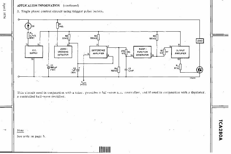
>'0
~ ...... \0 -..J >f:>.
---.j
APPLICATION INFORMATION (continued)
3. Single phase control circuit using trigger pulse bursts .
01
D.C.
SUPPLY
16
11
+1· C1 680fJF (16V)
ZERO
CROSSING
DETECTOR
C2 1+ 1IJF
(16V)
Vcontr «7V)
R3 330k.!l
DIFFERENCE
AMPLIFIER
R4 150kn
RAMP
FUNCTION
R6 100kn
141 GENERATOR ~
C3 1,5nF
82 kn
OUTPUT
AMPLIFIER
LOAD
This circuit used in conjunction with a triac, provides a full-wave a. c. controller, and if used in conjunction with a thyristor, a controlled half-wave rectifier.
Note
See note on page 5.
~ n » ~ CD o :I>

,TCA·2'80A
II [I APPLICATION INFOt1MATION (continued)
1000
P (W)
Rd (kn)
C (x1OIJF)
100
10
\ \ ,
\
/ '"l ~
/ I
J
'\ ,/'''
"->< /"
........ Rd 1/ ........
~ r- - -- -,/'
,/'
/' ,/
//
7Z63999
V,
Rd [
D~~ ~ 13
TCA2BOA I ; ~C1 16
1Z6199~
C1 min I--~ I--~
~ 1---"' .......
./
Pin Rd p ..... ~ ......r-
-kl"'" - ~ ~ I-~~ ~
11 2 3 4 5 6 7 8 9 10 11 12 13 14 15 16 17 18 Itot (rnA)
Graph for determining the values of Rd, dissipation P in Rd' and minImum recommended value of C 1 as functions of Itot for the circuit conditions shown (with diode D) Itot is the maximum average current through D5, and is the total of the current consumed by the'IC and by the' external components. It should be noted that certain applications like the time proportional controller require an up to three times higher value of C 1.
8 II April 1974

II II APPLICATION INFORMATION (continued)
Note
1000
P (W)
Rd (kn)
C (x10~F)
100
10
1
7271000
Vs
Rd
13 ~ TCA280A I :~C1
1'6
"7~l91~
tC1~ f--~ -\ ....... ........ 1 ~
'\ v~ I I I f--f--
"- V PinRd _ -./
>( ........ _ ........ .,...;.
/ ....... / ~
..... Rd / ./ --/ / .......... ... - "7 -- -r r- - - - --~-f'--/ Rdm1n r-r-
V
1 2 3 4 5, 6 7 8. 9 10 11 12 13 14 15 16 17 18 I tot (mA)
Without diode
TCA280A
This graph i~ not suitable for phase control applications; use the graph on page 8.
November 1974 II 9
----

TCA280A
II II APPLICATION INFORMATION (continued)
100 \ .\ \' , . \\ \ \ \~ ~ "\ \~ 5W
r--...:
10
\\ '\
~ " ~~ \ ~ r-..... to ~ \ ~ " '\
" " ,
" ~ \. . ' . ........ \ , " ~ " \ " ~ \ '\ ~ " " \ "- "
, ~~ ~
\ ", " ~ r---.. ~ i\ "
, ...... r--....
" \
"- r"", I\. "-~
" " ./
K' .......
......... ~
7Z63998 Vs
R.
o(D r;--13
I TCA280A I :~C1 16
1l6199~
I I I 10W i'-.. ........ Rdmin
i""ooO I ..... 1'1: r-
1'--.' I I' ~~ II
" -'f-i---
'Jr--, i""'--
~ i'-.. If
i"j r-
~ ~ r- ---r-V r-r-~
r--r-r-. ~ i:--
~ 2W"""'" .----F= I' -..... 1"'-
r-... -1W"
f""'-. i'-..fo.,. ------
Vs= 380V,,-
220V,,-
110Vrv
90Vrv
70Vrv
50V,,-
30Vrv
0,11 2 3 4 5 6 7 8 9 10 11 12 13 14 15 16 17 18 Itot (rnA)
Graph for determining the value of Rd and correspondingdissipation at different mains voltages for the circuit conditions shown (with diode D) Itot is the maximum average current through D5, and is the sum total of the current consumed by the Ie and by the external components.
10 II April 1974
I /..,

II II APPLICATION INFORMATION (continued)
Note
100
Rd IUl)
10
~5W
~ ~ \ ." ~ ~ ~_'\
"- "\. , I\, ~" \l\ , f\
r\.
t-- j---
7Z71001
,Vs
R'~ 13 11
ir'" I"j" 10W
I"-~ ~ ~ ~ r-...: 15W
.1 I ~ ~ , ~r--. Rdmm .... ... r-
1,\ ....... i:""-. -'" ~ i r-!-...
I\'\. l\ -....~ I' II -t--~~ \ ~r--. fJ..
"r-... r--.... I, '1 r-~ I" ~. r........ ....... ,
~ I/, ,,~ l"-I'-. ...
'I'-. 1"'--f".. ~ t ~ "
r-..... 1\ t"- b-- r-- .... i' N ......
f".. k: ~ t"- r-r--~ ~ ~ r--\ ~ r--~
l-t-- I"-\ r-.... k ~ r-
~
"" -- .... ,....... l'
I • .)"" \ l""'- T"
1W' ,..... -1"-
l'l' 2W\ i""-t-I'-o, I -1"'-1-1-1"'-1"--
Vs :::
380V~
220V",
110V", 90V rv
70Vrv
50Vrv
30Vrv
0,1 1 2 3 4 5 6 7 8 9 10 11 12 13 14 15 16 17 18 I tot (mA)
Without diode
TCA280A
This graph is not suitable for phase control applications; use the graph on page 10,
November 1974 11

e F
TCA280A
II II APPLICATION INFORMATION (continued)
1000 7ZU!I97
.. , "'Ioc"
.. " """ ~""~~ VG= '~ ~ 2V
~ ~ ~~V I\.. /1 4V
~ ~~~~~ i' )'~ 100
.,' i\..""" , i\.. i\.. i\..i\.. '\ ,,~ ~
RGniin_ -' '\ ~\. f- i-- i-
10
"\ ~ ~\ :\.
\
100 IG (rnA) 1000
Graph showing RG as a function of IG of the TCA280A for various values of VG. The minimum value of RG at which the current 110 is kept within the specified limits is 22 Q.
12 II April 1974

II APPLICATION INFORMATION (continued)
20
I tot
(mA )
15
10
5
r-
~-
~
t---I tot max
t--- --
~ ~ Iiiiii''''"
I- - -f-o
1/ ~~ ~
~ ~ !fBi! po ... ~
--- -- - .- -l-
V 1/ V V
...... V V .... ~ V 1/ V ~ ~ ~ ....
~ ~ ~ ~ ~ ....... ~ ~ po'
100
II TCA280A
7Z71017
I " ~~ - .~
S~,L ~~. ~- f-- --f---- ~ ~
" \K ';
.~ ~ i- --- ~ - .~ - - 3V
l/ V ./
V 1/ 1/ 2,5V
~ V
~ V [.....-' ~~ ~ ~ 2V
V ~ r;. t:::: ~ .... ~ ~ 1,5V ~.
V r:~ t::::- t:::: ~ ~ ~ ~ ....... ~
200 300
= Graph for determining Itot corresponding to a given IG with Vc as a parameter. = Once Itot is kno~n, the required values of Rd, RG and C 1 can be found. from the graphs on pages 8, 9, 10, 11 and 12. Note that this graph can be uesd only if the highest possible RG is used.
April 1974 II 13

I
I I I

Preliminary
Ii II TDA0555,D
TIMER
TheTDA0555D is a monolithic timer, equivalent to the NE555, however it is mounted in a miniature plastic package. It is a highly stable controller capable of producing accurate time delays or oscillations. In the time delay mode of operation the timer is controlled by one external resistor and capacitor. For operation as an oscillator the frequency and the duty factor are both accurately controlled by two external resistors and one capacitor. Additional terminals are provided for triggering or resetting. The circuit maybe triggered and reset on the falling-edge ~f a waveform.
Features
• Timing from microseconds to hours
• Operates in both astable and monostable modes
• Adjustable duty factor
• Output can source or sink 200 rnA
• Output and supply TTL compatible'
• Temperature stability 0, 005%;oC
• Normally-on and normally-off output
• Operating ambient temperature: -25 to +85 0C
• Miniature plastic encapsulation
CONNECTION DIAGRAM
TRIGGER 2
OUTPUT 3
RESET 4
PACKAGE OUTLINE (see general section)
SO-8 (SOT-96A); plastic 8-lead flat pack.
August 1976 II
Vp
DISCHARGE
THRESHOLD
5 CONTROL VOLTAGE
7Z75108
--

N
::x:c ~ ~ f-' \0 -.J Q\
1111111
CIRCUIT DIAGRAM 5
• •• " , ,08
R8
6
3
20----~~------+_------~
4
7
R6
R4 7Z72848
J
--t' o » o U'I U'I U'I o
""C "i ~ 8'S-III "i
.,<

Preliminary
II II TDA0555D
RATINGS Limiting values in accordance with the Absolute Maximum System (lEe 134)
Supply voltage VP-VN max. 18 V
Temperatures
Operating ambient temperature Tamb -25 to +85 °e
Storage temperature T stg ~65 to +125 oe
Junction temperature T j max. 125 oe
Power dissipation in free air; T amb = 50 °e
Mounted on a ceramic substrate of 4 cm2 Ptot max. 470 mW derating factor for T amb > 50°C l/Rth 6,3 mW/oe
Mounted on PC board of 4 cm2 Ptot max. 310 mW derating factor for T amb > 50 oe l/Rth 4,2 mw;oe
August 1976 II II 3
· · · · · ·

TDA0555D
II I
Preliminary
CHARACTERISTICS at VP.= 5 to 15 V; VN = 0 V; Tamb = 25 °C unless otherwise specified
Parameter Conditions Symbol min. typo max. Unit
Supply voltage Vp 4,5 - 16 V
Supply current 1) Vp = 5V;RL =00 Ip - 3 6 rnA V P = 15 V; R L = 00 Ip - 10 15 rnA
Timing error (monostable) RA = 2 to 100 kQ initial accuracy C = 0, 1.!JF - 1 - % drift with temperature - 50 - ppm/oC drift with supply voltage - 0,1 - %/V
Timing error (astable) RA; RB = 2 to 100 kQ initial accuracy C = 0,1 flF' - 2,25 - %
. drift with temperature - 150 - ppm/oC drift with supply voltage - 0,3 - %/V
Threshold voltage - 2/3Vp - V
Threshold current - 100 250 nA
Trigger voltage Vp = 15 V - 5 - V Vp= 5V - 1,67 - V
Trigger current - 2 - f.!A Reset voltage 0,4 0,7 1,0 V
Reset current - 0,1 - rnA
Control voltage level Vp= l5V 9 10 11V Vp= 5V 2,6 3,33 4 V
Output voltage; LOW Vp = 15 V; Isink = lOrnA VOL - 0,1 0,25 V Vp = 15 V; Isink = SOmA VOL - 0,4 0,75 V Vp = 15 V; Isink = 100 rnA VOL - 2,0 2,5 V Vp= 15V;Isink =200rnA VOL - 2,5 - V Vp= 5 V; Isink = 5 rnA VOL - 0,25 0,35 V
Output voltage; HIGH . Vp = 15 V; Isour~e =200 rnA VOH - 12,5 - V V p = 15'V; Isource = 100 rnA VOH 12,75 13,3 - V Vp= 5 V; Isource = 100 rnA VOH 2,75 3,3 - V
Output rise time tr - 100 - ns
Output fall time tf - 100 - ns
Discharge leakage current - 20 100 nA
1) Supply current when output HIGH: typo 1 rnA less.
4 II August 1976

II II TDA1024
A MAINS-ZERO TRIAC-TRIGGERING CIRCUIT
The TDAI024 is a monolithic integrated circuit intended for use in ON/OFF control of triacs in static switching applications. It incorporates zero voltage point triggering to minimize radio interference. The TDAI024 is mainly intended for applications such as switching resistive loads and replacing mechanical thermostats in, for example:
- central heating installations, - washing machine heaters, - water heaters, - smoothing irons.
QUICK REFERENCE DATA
Supply voltage (via dropping resistor)
Average supply current
Trigger pulse width
Max. trigger current capability
Vs 17(av)
tp
12max
PACKAGE OUTLINE plastic 8 lead dual in-line (see general section).
June 1976 II II
mains voltage
typo 10 rnA
typo 195 I-Is
> 100 rnA

--f
TDAI024
II BLOCK DIAGRAM
mains control circuit (¥s) d.c. supply
I I t7 +8
1 ZENER-LIMITED - -, D.C. SUPPLY
common
control input
5 INPUT ~
reference input
- ........ BUFFER
4
Funcnons of the TDAI024 are:
-
TDA1024
COMPARATOR
.ff
3
hysteresis control
- a comparator with Schmitt -trigger action.
II
mains synchronization
I t6
ZERO-CROSSING
DETECTOR -
t CONTROL -.-
GATE·
t OUTPUT
STAGE
2 f-+-
7Z71368
- trigger output
This circuit compares the control voltage at pin 5 with the reference voltage at pin 4 and switches on when the control voltage exceeds the reference voltage. The hystere sis of the circuit is adjustable between 20 m V and 300 m V by selection of the value of a resistor connected betweenpin3 and pin 1.
- an input buffer circuit with high input impedance and low output impedance. This circuit presents a low impedance to the comparator input so that the hysteresis of the circuit is independent of variations of the input voltage.
- a control circuit d. c. supply which provides a zener-limited nominal 6,5 V supply, at a current of up to 30 rnA, for application to the input bridge.
- a zero-crossing detector which produces an output when the sinusoidal voltage applied to pin 6 passes through zero; advantage of this mode is minimum radio interference-.
- a control gate which inhibits the output trigger pulse from the TDAI024 unless there are outputs from both zero-crossing detector and comparator.
--an output stage which delivers a positive-going, mains-synchronized triac trigger pulse whenever the control gate is activated. The output from this stage is currentlimited and prot.ected against shQrt-circuit. Since the current and voltage in the load must be in phase for mains-synchronized switching, the applications of the lDAI024 are restricted to the switching of resistive loads.
2 II June 1"976

'"a' ::s Cll
...... . \0
'-..J 0\
w
~=----- -=-~ - -=-----=- -~ --
CIRCUIT DIAGRAM r -- -ZENER:LiMl"iEo -- ~ - - - - - -- -ZERO:CR~IN~OETECi-OR - - i , SUPPLY 8 I 6
I 02 r' I i70 .1, , I
01
1 0 I i I :: ! ~- ________ ~ ___________________ ~~J
r-------~-----------------------------~-----------~-;---------,
, Q , I I I I b
40----~--~_+----------r_--_+----~
08
INPUT BUFFER COMPARATOR CONTROL GATE OUTPUT 3
-------~-----------------------------~-------------~-------~~~
-t C » -o ~ ~

TDA1024
II II RATINGS Limiting values in accordance with the Absolute Maximum System (lEC 134)
Voltages
Supply voltage (pin 7)
Voltage on pins 2,3,4,5 and 8
Currents
Supply current (pin 7); average value peak value
Current at pins 4, 5, and 6
Vs V2- 1; V3-1; V4- 1 ;
VS _1 ; V 8-1
± 17(av) ± 17M
14; IS; ± 16
Non-repetitive peak current at pin 7 (tp<SOflS) ± 17SM
Output current (pin 2); average value - 12(av) peak value (tp<300 vs) 12M
max. 8 V
max. 8 V
max. 30 rnA max. 80 rnA
max. 10 rnA
max. 2 A
max. 30 rnA max. 400 rnA
Temperatures
Storage temperature T stg
Tamb
-55 to + 125 °c Operating ambient temperature
Power dissipation
Total power dissipation
4
500
Ptot (mW)
250
o o
II
, 50
-20 to +80 °c
see derating curve below
7Z72624
" "Rthj-a = 200 °C/W_ I-~I-
~ 1'1
" ~ " " " 100 150
II February 1976
III

II II II TDAI024
I~l ==========~================================ 1.,1
CHARACTERISTICS at T amb = 25°C; f = 50 Hz
Zero-crossing detector
Trigger pulse width at 16(rms) = 1 rnA;
V8- 1 = 5,5 V
Synchronization resistor
Trigger output (pin 2)
Max. current capability at V 8-1 = 5,5 V
Trigger current capability
Max. trigger voltage at -12 = 100 rnA
Gate resistor
Comparator at V8 - 1 = 6,5 V
Hysteresis; pin 3 not connected; 13 = 0
Hysteresis; pin 3 connected to common; V 3 = a Input current at V
4_1
> V5 - 1 (pin 4)
Input current (pin 5)
Control circuit d.c. supply (pin 8)
Voltage on pin 8 at 17(av) = 10 rnA
IC current consumption (with min. hysteresis) pins 2 and 3 not connected; V5 _1 > V4-1; V8 - 1 = 5,5 V
IC current consumption (with max. hysteresis) pin 2 not connected; pin 3 connected to common;
V 5-1 > V 4-1; V8-1 = 5,5 V
Total average current consumption (pin 7)
Mains dropping resistor
Mains dropping capacitor
June 1976 II
typo 195 I-ls tp 130 to 265 I-ls
see Fig. 3
- 12 max > 100 rnA
see Figures 5,6,7 and 8
V2-l > 4 V
see Fig. 4
6. V5-4 10 to 30 mV
6. V5 - 4 typo 300 rnV
14 < 5 I-lA
IS < 5 I-lA
V 8-1 typo 6,5 V -5,5 to 7,5 V . . -
IIC < 1,8 rnA
IIC < 3 rnA
see Fig. 9
see Figures 10 and 11
see Fig. 12
11 5
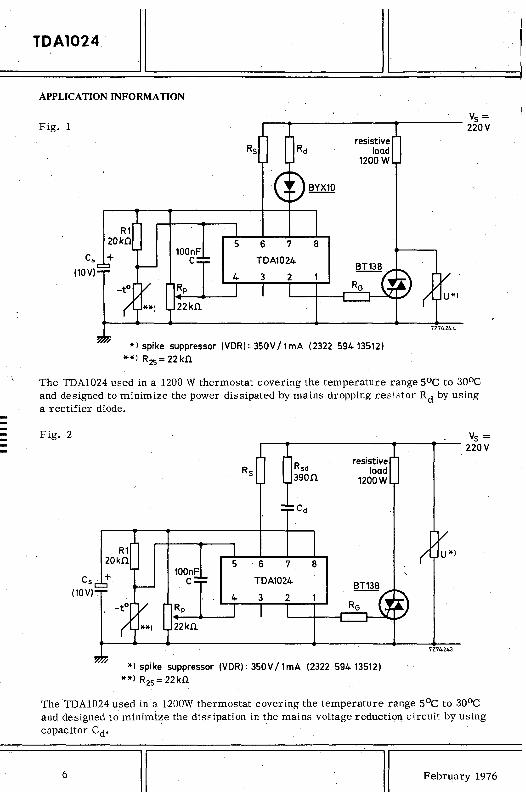
TDA1024'
II APPLICATION INFORMATION
Fig. 1
Cs
(10V)
resistive load
1200W
*) spike suppressor (VDR): 350V/1mA (2322 59413512) **) R2S = 22kfi
Vs= 220V
The TDAI024 used in a 1200 W thermostat covering the temperature range SoC to 30°C and designed to minimize the power dissipated by mains dropping resistor Rd by using a recti:!:ier diode.
Fig. 2
Cs
(10V)
100nF C
resistive load
1200W
*) spike suppressor (VDRI: 350V/1mA (2322 59413512) **) R2s = 22 k.Cl
U*)
7Z74243
Vs = 220V
The TDAI024 used ina 1200W thermostat covering the temperature range SoC to 30°C and designed to minimize the dissipation in the mains voltage reduction circuit by using capacitor Cd'· .
6 II II February 1976

II II TDA1024
APPLICATION INFORMATION (continued)
Design data for the two previoUfl circuits (for other circuits the same sequence of component value selection must be used):
BT138 triac with: V GT = 1, 6V at 0 °c . lCT = 72 rnA at 0 °c
Mains voltage: V S = 220 V Triac load: 1200 W
lL < 60 rnA
Component values and circuit parameters:
parameter Value Fig.l Fig. 2
trigger pulse width : tp (i-ls) 105 105
sync. resistor : RS (kQ) 180 180
gate resistor : RC(Q) 33 33
average gate current : 12(av) (rnA) 3, 7 3,7
min. required supply current : 17 (rnA) _ 6,5 6,5
mains dropping resistor : Rd (kQ) 10 -smoothing capacitor : C s (i-l F ) 470 470
power dissipated by Rd :PRd(W) 3,2 -mains dropping capacitor : Cd (nF) - 270
power dissipated by Rsd : PRsd
(mW) - 190
~,) See BT138 data sheet.
February 1976 II
Figure
':,)
3
4
6
9
10
10
11
12
12
7
--

TDA1024 II
1000
Rs (kfi)
500
I 1
JA 1/ , rl ~~ 1(/
J I
J. '{/
V"
I I I Vs=380V
J / I
II I JI
I If 11/
I J I /1
'/ 1/,
JV ./ II V
r ~
V V
?Z72625
~4~V' -/220V
/110V
250 500 ~p (~s) 750
4
~~ t't:-. ~ r--,r--
2
o o
\ , \ \
' l'- 'I" r-... 1\.,'\ 1'\1 ....... i'...
,\.~I'\ II\. I\. 1'\,'\
1'\,'\
1\ \'\ \ I'\.
1\ 1\ , , 1\ \
1\ 100 \'
....... ..... ...... .....
, ...... '\ I'
'\ " " i .....
\. 1'\ I\. .....
I\. \.
'\. I\.. -e-~8 50
8 II
?Z72627
....... RG = ....... ·18.fl
..... r---~
...... l'-
/ :(i-, 3~-c-.. 'I..
'\ 3~-~6 ~~47 ~
100
Vs
tp
Fig. 3., Synchronization resistor (RS) 'value as a function of required trigger pulse width (tp) with applied mains voltage (V S) as a parameter. Tolerance for RS : ± 5%
for Vs : ± 10%
TDA1024.
Fig. 4. Gate voltage (VG) as a function of trigger current (I2) with gate resistor (RG) load lines.
II February 1976

I~: ========~II =========================:::...:::11 =====TD==A 1==024===== III
I
Figures 5,6,7 and 8, on the next two pages, have to be used with the circuit below. They show the maximum average trigger current 12(av) as a function of the value of RG with the value of RS as a parameter for Vs = HOV; 220 V; 240 V; 380 V respectively.
February 1976
Rs
TDA1024
2
II 9

TDA1024
II II 200
150
100
50
o o
200 ---
150
100
50
o o
10
7Z72628
1\\ ~ \ \1\ Vs:= 110 V 1\ \ \ \ 1\ ~ "
\1\\ \ \ \ \1\ \ \
\ i\ ~ \ \ \\ \ \ \ \ \. l\,\ , \ \ \ \ :\ 1\ \ \.
\ \ \ \ ' \ '\. \' \ ,\ \ \. \ "\ "-~\I\ ' \ ,
" "'\ ,I' ........
\' \l\. I\, \ " ).. ...... , ...... 1'-,
'l\ \. r\ " "- ........ , I""'-~ r----.. ~ ~90 ~ ........ ........ , ""'" ....... r----.. ...... r-.... r-r--. / 330- -, I\.. " ........ ~ !'..... I-- 1'270-, .............. ......... .......r---.. r-r- r- -r- ~ ~
-"- i'I'... ........ ........ !'..... I-- r-r-..... ~ I
~ ~ ......... ........ ........ ........ -r-r- -r-r- -I--I--I-- roo- I-'" "'-H= -r--.. I-- r- I--- -.......: ::;---...... -:;-r- l""-I--I--h r-r- -l""-I-- -rot r-~ -Rs=68kfil 82 1100 1120 1150 11 180 1220
I I I I il I 5 10 12 (av) (rnA) 15
Fig.S
7Z72629
\ \' \ \ , \ ~ ~ 1\ Vs = 220V
\\ \ \ , \ \ \ \ , 1\ 1\ \ 1\ ~ 1\ .h \ \ \ \ \ \. \ 1\ \ \ 1\ i\.
\ ,\ \1\ \ r\ \ ' r-.. r\. \\ 1\ \,\ "\ i\. '\ "-\ \1\ i\. I\, ,
"' ........ \\ 1\ \\ \. I\. " ...... ~ ...........
\ \1\ \. i\. \ I\. ..... , ........ , 1 Mfi r-
\ 1\ ~ I\.. " 1"'\ r-..... , ........ , ........ V 820 kfi
\ 1\\ \'\ i'... ........ r-..... ............... ........ ........ - / V/ 680-r-.
'- ........ t"'-_ 560-r-. , \ l\. "\ ,~ r-..... I"'-'" I' I"-.... ........ ....... ........ ....... ....... -I-- """" /4 ~
'\ l"\ "- "' ~ ........ ~ ...... ...... ....... ....... ............. ---r- ----' n. I-- roo-- I--. , ........ ~ ........ r-..... r-.... r-. ....... ....... -....... -r--- -r-I--
,.... I--r--r--.. - - - r- '--r-..... ~ r-.... r- r..:::: r-----=---r-:: ~ I-- -- - r-- ~
Rs=120 kfi I 1501 180.1 2201 2701 3301 390 470
I I II I I I 5 10 12(av) (rnA) 15
Fig.6
II February 1976

II 200 DIlll[\ \\ 1\
f- ~\I\' \ \ \ \ \ '
f- \ \\ r\ \ f-
\\ \ \ \ 1\ \
150
\\ \ 1\ \ \ \ \ \
, \\ ~ ~
\\\ \ \ \ \ \' \ \\ \ [\
100
'\ \ \ \ , ~\ \\ \ '\ \\ \ i\ , 1'\
50 \ \. ~' ~ I\: ~ ~ '" ~ " t'--.. r----
L ....... ~
J Rs=120kO/
o o
I /
200 \\1\ \ \ \ 1\ ~ \ \ i\ \ \ \ ,
\ \1 \ 1\ \ \ \ \ 1\ \ , \ \ , 150
\ \ \ L\ \ \ !\ \ \\\ ' \ \ \l\ ~ \ ~
,1\ , \ \ \ , _ 100
\ \ \ \ \ I" \\\ r\
\ \
\.
I'\. ~
'" I'\. "-"-:::-.. ........
\ \
\ \
1\ , \
'\ r'\.
\ \'\ '" 50
\,\ .'\. ...... " ~
'\ " ........ ~ ..... ~ ~
I\, r\
r\. '" t\. ...... "
~ ~
~ ~ 'i'.. I' ~
....... i'.. I'-. ........ ~ r--..... 1000....
1000.... --........ 1"-0.. I'-.
~ 1000.... r--/150 1/ 180
I II 5
\. , \
\ \. \
\ '\. \. '\.
i\. l'-.. r\. t\.. ~ i'...
" ~ ~ '~ ........
~ ........
r-..... I ........
I'-. ['.. ~ """"" t--~ r-r.::: ....... r-~ r-c:::
o o
February 1976
RS=27Oknl
I 3301
I 5
II TDA1024
7Z72630
Vs =240 V
i'... "' ....... '" ......... , , /820
......... ........ --r- 680-r--....... ........ r-. / /~601-1000.... -- ....... r- -- ~
r--....... ....... r-1'-00.. I--. -::
....... ....... ....... -....... r- r-r-r-- I--. .....::: ~ r-- I-- -:;---.::: :;-I'- -I--I--r-r-- ..... - r-I--r-. I- -~ /220 /270 /330 390 !470
I I I I 10 12 (ovl (rnA) 15
Fig. 7 7Z72631
Vs= 380 V
f'.. I'
~ 'r--... 1,8
' ....... "'r--... / 1,5-r--
r-.... i'-...... r--..... //; 1,2-r--r--...
~ ' ...... --r-~ ....... r-~ /1/:: / 1Mn
~ ....... ........ :--r...... r-r- ~ i""- 7'--.... ~ ....
1000.... ............. ....... -r-I'- -....... r-t-- 7 7' -1'-00.. ---- r-r-r- -r-r-r- ..:2 -r- io-- -- -I-- I--'- ~
:-.. ----I--I'-r--I'-I'-I----- io--
,-.. ....... - 1'-00.. I- .... r-,.,. 390 4701 560 6801 8201
I I !I 10 12 (ovl (rnA)
15
Fig. 8
II 11

TDA1024
15
·10
5
o o
II
I' I'
17 ,/
1/ 1/
,/
1/ 5
13=0
~
I' 1/ 1/
Li' 1/
'" 17 1/
1/
10
Vs
! 17
7
TDA1024
7Z72632 . , / , 1/ 7' 1/
1/ , 1/ 1/ , 1/ , 1/
'/ '/
1/ , 1/ 1/
t(.... 7~V3=0 1/
iI'"
15 I7(ovl (mA) 20
Fig. 9. Minimum required supply current (17) as a function of maximum average trigger current (12(av»' with hysteresis setting as a parameter. 13 = 0; min. hysteresis. V 3= 'a; max. hysteresis.
12 II II Fepruary 1976

16
Rdmax (k.n.)
February.·1976
12
8
4
'0 o
TDA1024
I ,
, \
1\ \ ,
Vs
7
\ 1
\ \ , ,
\ , \ ,
\
" \ \, \ \
\ ,\
" 11
1\ y\
\\
\\
,'\.1\ , \
:y
\. -""'~
""\
" '"
10
8
+
7Z74247
\
I'\.
Vs= 380V
1 I 1 I
i46v I\. 'X 1 1
,,1'1. l\.1~
I'" 2?9V
I 1 1 I
..... 110V ..... "'"
Cs
(10Vl
..J
I '
1200
Cs
Rdmin
800
400
0 20 I 7min (mA) 30
Fig. 10. Value of Rd max as a function of 17min with supply voltage (V s) as a parameter. Also shown is the value of the smoothing capacitor (C s ) as a function of 17min,
II 13

-
20
15
10
o o
It . 1 \ , \
~ ,
Vs
-
--
\ , IIIl '11 \
~ , 1\ \
1\ 1 \ -, 11 -' \ \ ~ '-,
\ \ \ 1\ \ \
1\ 1\ 1\
\ \.
"-'.
" '. '\.. I"'.
"-"
7Z72633
\ \ --with diode BYX10
---without diode BYX10
\
\
~ \
\
1\
\ r ..
~ , '. , ",
\ ~ -, ,
\. '\ Vs =380 V \. -, I ... ". ~ I\.. I"
[ .. , :-.. '" ...... I ...
"'--" " ..... " .....
'" r-.. i'.. I"'- - .... 380 V
r-.. I' ~'''' ' "'~ ... '1"'-t--t-... ..... '.~. ~40V ..... .... - ~2~V .. .... - r-.... L I
-r-I_ i-I '-'- 220v -I-WV -1-_ 11°} I J I I 10 20 Rd (kIl) 30
BYX10
+ Cs TDA1024 (10V)
Fig. 11. The power dissipated by mains dropping resistor Rd (PRd) as a function of its value with the supply voltage (Vs) as a parameter.
14 II II February 1976

,,1'1
'ill
II I
Ii I
100
PRsd (mW
0
)
500
j .~
WV J I
., 1/
I/, V o o
II
PRsd
II
j
1 II
ii-71/
I 'J 1/11 r/v
JV It'
10
1272626
1000
VS= t-- I-
Vf2~V l-I-Cd
J/240V (nF)
~P'" Cd l-I--l-
500
o 20 17 (mA) 30
II TDA1024
Using a capacitor for mains supply voltage dropping.
Vs
17 J
TDA1024
1274250 "
Fig. 12. Power dissipated by the dropping resistor (PRsd) and the dropping capacitor value (Cd) as a function of the current into pin 7 (I7) with the mains supply voltage (V
S) as a parameter.
February 1976 II 15

II

, ..•
1
,:1
II
II II
~i 'I II
I
I
I
SPECIAL CIRCUITS
--

TYPE SELECTION
Special circuits
SAAll14; Z
TDA0319D.
- 4-MHz clock circuit
- dual voltage comparator
TDA0723D - precision voltage regulator
TDA3081; TDA3082 - seven-transistor array
II
1,1
II November 1976

II
4 MHz CLOCK CIRCUITS
SAAl1l4 SAAll14Z
The SAA1114 is a C-MOS integrated circuit, particularly suited for crystal controlled clocks powered by a single battery. It contains an oscillator, a 22 -stage frequency divider and a driver for a unipolar stepper motor. With an oscillator frequency of 4, 1943 MHz, the output is a 1 Hz pulse of 31,25 ms duration with a current sinking capability of minimum 6 rnA. The SAA 1114Z is the same circuit, but has. in addition an alarm output signal.
Features
• Oscillator frequency: 4 MHz
• Output for unipolar stepper motor
• Single battery power supply
• Current consumption: typo 50!JA
• Output signal for alarm (SAAll14Z only)
CONNECTION DIAGRAMS
OSCILLATOR OSCILLATOR VN OUTPUT OUTPUT
OSCILLATOR OSCILLATOR INPUT INPUT TEST
MOTOR n.c. MOTOR ALARM OUTPUT OUTPUT INPUT
ALARM OUTPUT
7Z76024
Note
The SAAll14 is internally protected against electrostatic damage. However, to be totally safe, it is desirable to take handling precautions into account.
PACKAGE OUTLINE plastic 8-lead dual in-line (see general section).
August 1976 II II 1
--

N
:> c ~ Q) ~
~ \0 ~ 0\
1111111
BLOCK DIAGRAM
note 2 . \ test alarm switch RL2
7 4 6
ALARM SIGNAL U .~ I GENERATOR .. ,
15
~ I L-22-STAGE
OIVIOER
MOTOR PULSE
I I I L-J1 I GENERATOR rrJ
7Z76028
VN I8
~
Notes
1. Recommended crystal: 4322 143 03111; trimmer: 2222 808 32409.
2. Connecting the test terminal (pin 7) to Vp speeds up the output by a factor 128 for rapid testing. No connection is necessary for normal operation, due to an internal pull-down.
Vp
3. A built-in clamping diode between the motor output and Vp acts as a current by-pass if the induced voltage- ot the stepper motor exceeds 0,6 V.
-en en l>l> l>l> ------~~ N

I II SAAl114 SAAl114Z
RATINGS Limiting values in accordance with the Absolute Maximum System (lEe 134)
Supply voltage (V N = 0) Vp max. 3 V
Input voltage (all inputs) VN to Vp
Motor output current (pin 3) ±I3 max. 50 rnA
Operating ambient temperature Tanib -20to+70 °e
Storage temperature T stg -30 to +100 oe
CHARACTERISTICS at Vp= 1,5 V; VN = 0; fo = 4, 194 MHz; Tamb = 25 oe unless otherwise specified
Vp > 1,2 to 1,7 V Supply voltage range typo 1,0 to 3,0 V
Supply current at RL1 = 00 Ip typo 50 ~ < 120 ~
Motor output frequency (see timing diagram) f1 typo Hz
Pulse width of motor output t1 typo 31,25 ms
Voltage drop across output transistor at R Ll = 200Q Vol typo 80 mV < 200 mV
Stability of oscillator at .6.Vp = 100 mV .6.f/fo typo 0,2xlO-6
The following characteristics apply to the SAA 1114Z only (with additional alarm output).
Duration of alarm signal; pin 6 at Vp
Repetition of alarm signal; pin 6 at Vp .
Frequency of alarm signal (50% duty cycle)
Voltage drop across alarm output at R L2 = 1 kQ
Test circuit
Ru
vp-__ ---.
T3
T2
f2
V02
22pF
22pF *1
VN----------~~---~
*1 5,5 to 40 pF 7Z76027
August 1976 II
typo 4 s
typo 32 s
typo 256 Hz
typo 100 mV < 250 mV
" .3
--
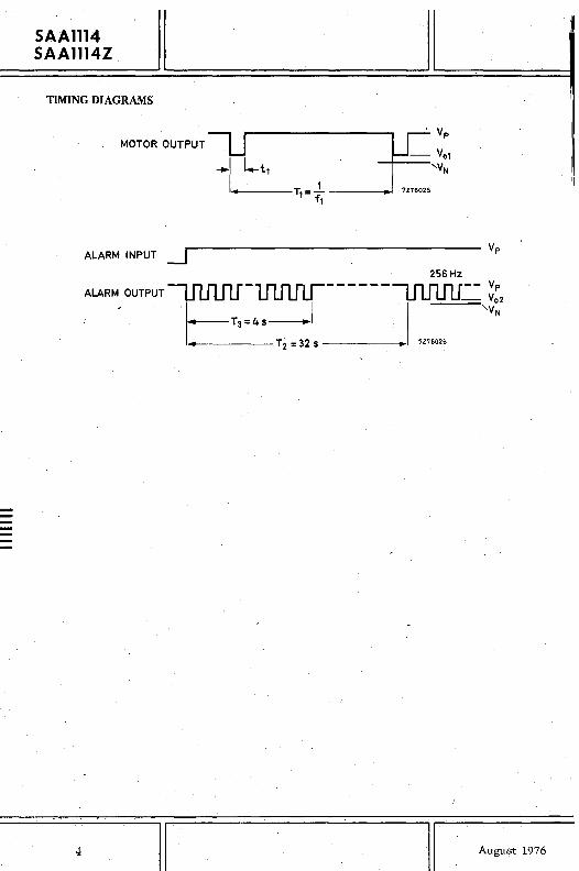
SAA1114 SAAl114Z
TIMING DIAGRAMS
MOTOR OUTPUT -U l. kt,
. V
f'~~ T1 = ..1. ---.. 7Z76025
f1
ALARM INPUT ...Jr---------------~ Vp
256 Hz
ALARM OUTPUT ---uuuu--1IlJ1JlJ-- - - - - --'JlfU1J.=~ ~:2
". 'I I 'I 'V '4----T3=4s----' N
• T 2 = 3.2 s .. ?Z76026
4 II II August 1976

, Preliminary
II II TDA0319D
DUAL VOLTAGE COMPARATOR
The TDA0319D consists of two independent precision high-speed comparators. It is designed to operate over a wide range of supply voltages down to a single 5 V logic supply and ground .. The uncommitted collector of the output stage makes the device compatible with DTL, TTL and C-MOS as well as capable of driving lamps and relays at currents up to 25 mAo The circuit is equivalent to the LM319, however it is mounted in a miniature plastic package suitable for hybrid modules and for applications where small dimensions are important.
Features
• Two independent comparators
• Operates from a single 5 V supply
• Typically 80 ns response time at ±lS V
• Minimum fan-out of 2 TTL gates (each side)
• Maximum input current: 1 f1A
• Inputs and outputs can be insulated from system ground
• High common mode slew rate.
CONNECTION DIAGRAM
GROUND (1) OUTPUT (1)
+INPUT (1) Vp
-INPUT (1) -INPUT (2)
VN +INPUT (2)
OUTPUT (2) GROUND (2)
7Z75101
PACKAGE OUTLINE S0-10 (plastic lO-lead flat pack) (see general section).
August 1976
II I

N
>-c ~ ~ ..... '>0 '-l 0'-
CIRCUIT DIAGRAM (one comparator) Rl
R2
VR25 ~R24
fTIUl1
1 IH21~TR1~
to other circuit half
OVp
1---+--+---4.~O OUTPUT
1 TR17C ~R17 OGND
VN 7Z75088
-t C » o eN --.0 C
'"0 I-! .~ s·
s· ~ I-! '<
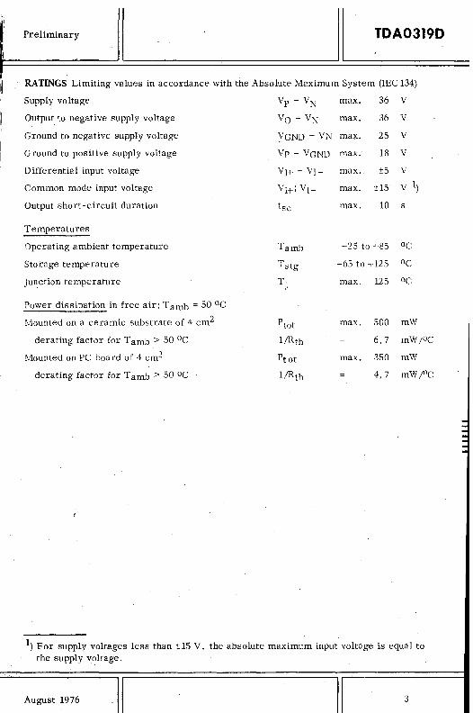
Preliminary
II TDA0319D
RATINGS Limiting values in accordance with the Absolute Maximum System (lEC 134)
Supply voltage Vp - VN , max. 36 V
Output to negative supply voltage Vo - VN max. 36 V
Ground to negative supply voltage VGND - VN max. 25 V
Ground to positive supply voltage Vp - VGND max.' 18 V
Differential input voltage VI+-VI- max. ±5 V
Common mode input voltage VI+; VI- max. ±15 V 1)
Output short-circuit duration tsc max. 10 s
Temperatures
Operating ambient temperature Taroh -25 to +85 °C
Storage temperature Tstg -65to+125 °C
Junction temperature T j max. 125 °C
Power dissipation in free air; T amb = SO °C
Mounted on a ceramic substrate,of 4 cm2 Ptot max. sao mW
derating factor for T amb > SO °c l/Rth 6,7 mW/oC
Mounted on PC board of 4 cm2 Pt ot max. ,'350 mW
derating factor for T amb > 50 oc l/Rth 4, 7 mW/oC
1) For supply voltages less than ±15 V, the absolute maximum input voltage is equal to the supply voltage.
August 1976 II 3

TDA0319D
II Preliminary
CHARACTERISTICS at V P = 15 v; -v N = 15 V; T amb = 25 °C unless otherwise specified
Parameter Conditions Symbol min. typo max. Unit
Input offset voltage RS < 5 kQ 1) 2) Vio - 2,0 8,0 mV
Input offset current 1) 2) Iio - 80 200 nA
Input bias current 1) Ii - 250 1000 nA
V oltage gain Gv 8 40 - V/mV
Response time 3) - 80 - ns
Saturation voltage - Vi < 10mV; 10=25rnA Vsat - 0,75 1,5 V
Output leakage current Vi> 10mV; Vo=35V 10 - 0,2 10 ~
Positive supply current Ip - 8 12,5 rnA
Negative supply current IN .." 3 5 rnA
Positive supply current Vp=5V;-VN=0 Ip - 4,3 - rnA
CHARACTERISTICS at Vp = 15 V; -VN = 15 V; Tamb =: 0 to +70 °C
Parameter Conditions Symbol min. typo max. Unit
Input offset voltage RS < 5 kQ 1) 2) Vio - - 10 V
Input offset current 1) 2) Iio - - 300 nA
Input bias current 1) Ii - - 1200 nA
Offset voltage range Vp =: -VN = 15 V Vio - ±13 - V
Vp =: 5 V; -VN =: 0 Vio 1 - 3 V
Saturation voltage Vp>4,5V; -VN=O Vi< -lOmV; Isink< 3,2 rnA Vsat - 0,3 0,4 V
Differential input voltage Vi - ±s - V
1) The offset voltage, offset current and bias current specifications apply for any supply. voltage from a single 5 V supply up to ±IS V supplies.
2) The offset voltages and offset currents given are the maximum values required to drive the output withinl V of either supply with a 1 rnA load. Thus these parameters define an error band and take into account the worst case effects of voltage gain and . input impedance. .
3) The response time specified is for a 100 mV inputstep with 5 mV overdrive.
4 II ,August, 1976

Preliminary
II TDA0723D
PRECISION VOLTAGE REGULATOR
The TDA0723D is a monolithic precision voltage regulator. The circuit is equivalent to the IlA723C, however it is mounted in a miniature plastic package suitable for hybrid circuits or other miniaturized applications. The circuit contains a temperature compensated reference amplifier, an error amplifier, a power series pass transistor and a current limiting circuit with access to remote shut down. The device can be used with positive or negative supply voltages as a series, shunt, switching or floating regulator.
Features
• Positive and negative supply operation.
• Line and load regulation
• Temperature coefficient of the output voltage: typo 0,003 % per °c • Input voltage range: 9,5 to 40 V
• Output voltage range: 2 to 37 V
• Operating ambient temperature: - 25 to +85 °c • Miniature plastic encapsulation.
CONNECTION DIAGRAM
CURRENT SENSE
-INPUT
+INPUT
Vref
PACKAGE OUTLINE. (see general section)
SO-lO; plastic lO-lead flat pack.
August 1976 II
CURRENT LIMITER
COMPENSATION
OUTPUT
7Z75105
1

TDA0723D
II Prellmina~y
CIRCUIT DIAGRAM 8 7
.... -----09
t----<J10
~ I
4 3 5 2 7275090
RATINGS Limiting values in accordance with the Absolute Maximum System (IECl34)
Input collector voltage (pin 7) Vc max. 40 V
Supply voltage Vp max. 40 V
Input-output voltq.ge. difference V7-6 max. 40 V
Output current 16 max. 150 rnA
Current from reference output 14 max. 15 rnA
Temperatures
Operating ambient temperature Tamb -25 to +85 °c
Storage temperature T stg -65 to +125 °c
Junction temperature Tj max. 125 °c
2 I II August 1976
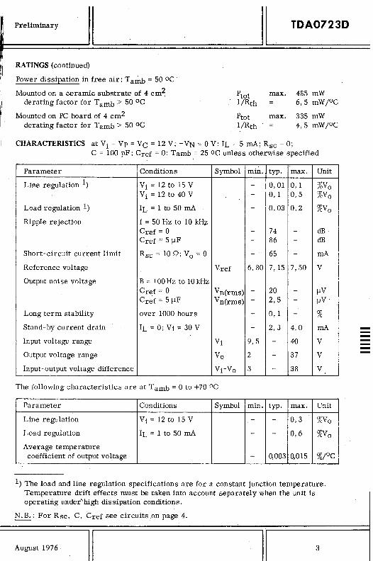
~ellmmary t I
RATINGS (continued)
Power dissipation in free air; T arcl, = 50 oc '
Mounted on a ceramic substr~te of 4 cm~ derating factor for T amb > 50 oc
Mounted on PC board of 4 cm2
derating factor for T amb > 50 oc
II
Ptot max. l/Rth
Ptot max. l/Rth
TDA0723D
485 mW 6,5 mW/oC
335 mW 4,5 mW/OC
CHARACTERISTICS at Vi = Vp = Vc = 12 V; -VN = a V; IL = 5 rnA; Rsc = 0; C = 100 pF; Cref = 0; Tamb = 25 oC unless otherwise specified
Parameter Conditions Symbol min. typo max. Unit
Line regulation 1) Vi = 12 to 15 V - 0,01 0,1 %Vo Vi = 12 to 40 V - 0,1 0,5 %Vo
Load regulation 1) I L = 1 to '50 rnA - 0,03 0,2 %Vo
Ripple rejection f = 50 Hz to 10 kH;Z; Cref = a - 74 - dB Cref = 5flF - 86 - dB
Short-circuit current limit Rsc = 10 Q; Vo = a - 65 - rnA
Reference voltage Vref 6,80 7,15 7,50 V
Output noise voltage B = 100 Hz to 10 kHz Cref = a Vn(rms) - 20 - flV Cr~f = 5 flF Vn(rms) - 2,5 - flV
Long term stability over 1000 hours - 0,1 - %
Stand- by current drain IL ::: 0; Vi ::: 30 V - 2,3 4,0 rnA
Input voltage range Vi 9,5 - 40 V
Output voltage range Vo 2 - 37 V
Input-output voltage difference Vi-Yo 3 - 38 V I
The following characteristics are at T amb ::: a to +70 oc
Parameter Conditions Symbol min. typo max. Unit
Line regulation Vi ::: 12 to 15 V - - 0,3 %Vo
Load regulation IL = 1 to 50 rnA - - 0,6 %Vo
Average temperature coefficient of output voltage - 0,003 0,015 %/oC
1) The load and line regulation specifications are for a constant junction temperature. Temperature drift effects must be taken into account separately when the unit is operating under~high dissipation conditions.
N.B.: For Rsc, C, Cref see circuits.on page 4.
August 1976 II 3
--

TDA0723D II
Low voltage regulator (Vo = 2 to 7 V)
8 7 4 6
Cref
R3 R1·R2f 00 d Of = R1+R2 or mInImUm temperature n t.
High voltage regulator (Vo = 7 to 37 V)
8 7 4 6
Rl+R2 Vo = Vref xR2"
TDA0723D
5
C
R1·R2 I R3 = Rl+R2 for minimum temperature drift
R2
R3 maybe eliminated for minimum component count.
4
7Z75091
regulated output
7Z75092
regulated output
II
. Preliminary
August 1976

DEVELOPMENT SAMPLE DATA Thrs information is derived from development samples made available for evaluation. It .does not form part of our data handbook system and does not necessarily imply that the device will go into production
SEVEN-TRANSISTOR AR~A YS
TDA3081 TDA3082
The TDA3081 and TDA3082 are monolithic integrated circuits each consisting of seven sep;:trate I}-p-n transistors on a common substrate. The transistors are capable of driving loads up to 100 rnA. At the same time the transistor geometry used gives maximum current gain at quite low currents, making the devices also suitable for small signal applications. In the TDA3081 the transistors are connected in common emitter configuration whilst in the TDA3082 the collectors are common. The transistor arrays are particularly suitable for driving light-emitting diodes and seven-segment displays as well as for general purpose applications.
QUICK REFERENCE DATA
. Collector-base voltage (open emitter) VCBO max. 50 V
Collector-emitter voltage (open base) VCEO max. 35 V
Collector current (d. c.) IC max. 100 rnA
Power dissipation: anyone transistor P max. 500 mW
total package Ptot max. 750 mW
CONNECTION DIAGRAMS (see page 2)
PACKAGE OUTLINE plastic 16-lead dual in-line (see general section).
August 1976 II I

TDA30-81 TDA3082 I
CONNECTION DIAGRAMS
TDA3081
Note: pins 5 _ are substrate.
2
I
TDA3082
7Z75103 7Z75102
II August 1976

'I II TDA3081 III TDA3082 ~il=====l ~====================~========== II RATINGS Limiting values in accordance with the Absolute Maximum System (IEC 134)
Each transistor
Voltages
Collector-emitter voltage (open base)
Collector-base voltage (open emitter)
Collector-substrate voltage (open base and emitter)
Emitter-base voltage (open collector)
Currents
Collector current (d. c.)
Base current (d.c.)
Power dissipation
Power dissipation: anyone transistor
total package (see derating curve)
Temperatures
Operating ambient temperature
Storage temperature
Junction temperature
VCEO
VCBO
VCSO
VEBO
IC
IB
P
Ptot
Tamb
T stg
T j
max. 35
max. 50
max. 50
max. 6
max. 100
max. 20
max. 500
max. 750
-40 to +125
-50 to +125
max. 125
7Z72851
August 1976
Ptot (mW)
1000
500
o -50
~
"
o 50
II
" ""'",-
~
" "'"",-100 150
Tamb (Oe)
V
V
V
V
rnA
rnA
mW
mW
oC
°C
°C
3

TD·A3081 TDA3082
CHARACTERISTICS at T amb = 25 0C unless otherwise specified
Collector-emitter breakdown voltage IC = 1 rnA; IB = 0 V(BR)CEO
Collector-substrate breakdown voltage IC = 1 rnA; I B = 0; IE = 0 V(BR)CSO
Collector-base breakdown voltage IC = 10 f1A; IE = 0 V(BR)CBO
Emitter-base breakdown voltage IE = 10 f1A; IC = 0 V(BR)EBO
D. C. current gain IE = 10 pA ; VCE = 5 V hPE IE = 1rnA;VCE=5V hPE IE = 20 rnA; VCE = 5 V hPE
Saturation voltage IC = 5 rnA; IB = 0,5 rnA VCEsat
IC = 50 rnA; IB = 5 rnA VCEsat
OPERATING NOTE
> 35
> 50
> 50
typo 7,0 6,5 to 7,5
50 to 300 50 to 300 30 to 200
typo 0,2 < 0,4
typo 0,4 < 0,8
As each collector forms a paras itic diode with the substrate, the substrate has to be connected to a voltage which is lower than the lowest collector voltage. To avoid parasitic coupling between the transistors, the substrate (pin 5) should be connected to signal ground.
V
V
V
V V
V V
V V
4 II August 1976


,I' "
"
",'1


INDEX I! II II ~IC. ========~=============================== '[
ilil 'III'
II
I
II
INDEX OF TYPE NUMBERS
The inclusion of a type number in this publication does not necessarily imply its availability.
Type No. Section Type No. Section Type No. Section
SAA1027 GI TCA410D A TDA0723D SpC SAAll14 SpC TCA520B A TDA0741D A SAAll14Z SpC TCA520D A TDA0748D A SAK140 GI TCA580 TC TDA1022 TC TAA960 TC TCA680B A TDA1024 GI
TAA970 TC TCA680D A TDA1034 A TBA221D A TCA770 TC TDA1034B A TBA673 TC TCA770A TC TDA1034D A TBA9l5 TC TCA770D TC TDA1034N A TCA2l0 TC TCA980 TC TDA1034NB A
TCA220 A TDA0301D A TDA1034ND A TCA240 TC TDA03l9D SpC TDA1458D A TCA280A GI TDA0324D A TDA3081 SpC TCA410A A TDA0358D A TDA3082 SpC TcA410B A TDA0555D GI TDA4250B A
A = Amplifiers SpC = Special circuits GI = General industrial TC = Telecommunications circuits
MAINTENANCE TYPE LIST
The type numbers listed below are not included in this handbook. Detailed information will be supplied on request.
SAA1028 TCA490
November 1976 II
Type No. Section
TDA4250D A
II
--

I I
I
- General ---.......
Amplifiers ---- T elecommunications'circuits ----- General industrial ----
Special circuits
Index and maintenance type list -

~.-----------
Argentina: r=APESA l.y.C., Av. Crovara 2550, Tablada, Provo de BUENOS AIRES, Tel. 652-7438/1478. Australla:"PHILlPS INDUSTRIES HOLDINGS LTD., Elcoma Division, 67 Mars Road, LANE COVE, 2066, N.S.W., Tel. 421261. Austria: OSTERREICHISCHE PHILIPS BAUELEMENTE Industrie G.m.b.H., Triester Str. 64, A-11 01 WIEN) Tel. 62 91 11. Belgium: M.B.l.E., 80, rue des Deux G~res, B-1 070 BRUXELLES, Tel 523 00 00. Brazil: IBRAPE, Caixa Postal 7383, Av. Paulista 2073-S/Loja, SAO PAULO, SP, TeJ. 287-7144. Canada: PHILIPS ELECTRONICS LTD., Electron Devices Div., 601 Milner Ave., SCARBOROUGH, Ontario, M1S 1 M8, Tel. 292-5161.
Chile: PHILIPS CHILENA SA, Av. Santa Maria 0760, SANTIAGO, Tel. 39-40 01. Colombia: SADAPE SA, P.O. Box 9805 Calle 13, No. 51 + 39, BOGOTA D.E.1., Tel. 600600. Denmark: MINIWATI AIS, Emdrupvej 115A, DK-2400 K0BENHAVN NV., Tel. (01) 6916 22.
Finland: OY PHILIPS AB, Elcoma Division, Kaivokatu 8, SF-00100 HELSINKI 10, Tel. 1 7271-France: R. T.C. LA RADIOTECHNIQUE-COMPELEC, 130 Avenue Ledru 'Aollin, F-75640 PARIS 11, Tel. 355-44-99.
Germany: VALVO, UB Bauelemente der Philips G.m.b.H., Valvo Haus, Burchardstrasse 19, 0-2 HAMBURG 1, Tel. (040) 3296-1. Greece: PHILIPS SA HELLENIQUE, Elcoma Division, 52, Av. Syngrou, ATHENS, Tel. 915311. Hong Kong: PHILIPS HONG KONG LTD., Compo Dept., Philips Ind. Bldg., Kung Yip St., K.C.T.L. 289, KWAI SHUNG, N.T. Tel. 12-2451 India: PHILIPS INDIA LTD., Elcoma Div., Band Box House, 254-0, Dr. Annie Besant Rd., Prabhadevi, BOMBAY-25-DD, Tel. 457 311-5. Indonesia: P.T. PHILlPS-RALIN ELECTRONICS, Elcoma Division, 'Timah' Building, JI. Jen. Gatot Subroto, JAKARTA, Tel. 44163.
Ireland: PHILIPS ELECTRICAL (IRELAND) LTD., Newstead, Clonskeagh, DUBLIN 14, Tel. 69 33 55. Italy: PHILIPS S.P.A., Sezione Elcoma, Piazza IV Novembre 3,1-20124 MILANO, Tel. 2-6994. Japan: NIHON PHILIPS CORP., Shuwa Shinagawa Bldg., 26-33 Takanawa a-chome, Minato-ku, TOKYO (108), Tel. 448-5611.
(IC Products) SIGNETICS JAPAN, LTD., TOKYO, Tel. (03) 230-1521. Korea: PHILIPS ELECTRONICS (KOREA) LTD., Philips House, 260-199Itaewon-dong, Yongsan-ku, C.P.O. Box 3680, SEOUL, TeJ. 44-4202. Mexico: ELECTRONICA SA de C.V., Varsovia No. 36, MEXICO 6, D.F., TeJ. 5-33-11-80. Netherland.: PHILIPS NEDERLAND B.V., Afd. Elonco, Boschdijk 525, NL-451 0 EINDHOVEN,.Tel. (040) 79 33 33.
New Zealand: Philips Electrical Ind. Ltd., Elcoma Division, 70-72 Kingsford Smith Street, WELLINGTON, Tel. 873156. Norway: ELECTRONICAA/S., Vitaminveien 11, P.O. Box 29, Grefsen, OSLO 4, Tel. (02) 150590. Peru: CADESA, Jr. 110, No. 216, Apartado 10132, LIMA, Tel. 27 7317. Philippine.: ELDAC, Philips Industri~1 Dev. Inc., 2246 Pasong Tamo. MAKATI-RIZAL, TeJ. 86-89-51 to' 59. Portugal: PHILIPS PORTUGESA S.A.R.L., Av. Eng. Duharte Pacheco 6, L1SBOA 1, Tel. 68 31 21. Singapore: PHILIPS SINGAPORE PTE LTD., Elcoma Div .• POB340, ToaPayohCPO, Lorong " Toa Payoh, SINGAPORE 12, Tel. 53 8811. South Africa: EDAC (Pty.) Ltd., South Park Lane, New Doornfontein, JOHANNESBURG 2001, Tel. 24/6701. Spain: COPRESA S.A., Balmes 22, BARCELONA 7. Tel. 301 6312. Sweden: A.B. ELCOMA, lidingovagen 50, S-10250 STOCKHOLM 27. Tel. 08/67 97 80. Swltzerland:PHILIPS A.G., Elcoma Dept., Edenstrasse 20, CH-802TZORICH, Tel. 01/442211. Tarwan: PHILIPS TAIWAN LTD., 3rd Fl •• San Min Building. 57-1, Chung Shan N. Rd, Section 2, P.O. Box 22978, TAIPEI, Tel. 5513101-5. Turkey: TORK PHILIPS TICARET A.S., EMET Department, Gumussuyu Cad. 78-80, BeyoglO, ISTANBUL, Tel. 45 32 50. United Kingdom: MULLARD LTD., Mullard House, Torrington Place, LONDON WCl E 7HD, TeJ. 01-580 6633.
United Statea: (Active devices & Materials) AMPEREX SALES CORP" 230, -Duffy Avenue, HICKSVILLE, N.Y. 11802;Tel. (516) 931-6200. (Passive devices) MEPCO/ELECTRA INC., Columbia Rd., MORRISTOWN, N.J. 07960, Tel. (201) 539-2000. (IC Products) SIGNETICS CORPORATION, 811 East ArquesAvenue, SUNNYVALE, California 94086, Tel. (408) 739-7700.
Uruguay: LUZILECTRON SA, Rondeau 1567, piso 5, MONTEVIDEO, Tel. 9 43 21.
V.,.zuela: IND. VENEZOLANAS PHILIPS SA, Elcoma Dept., A. Ppal de los Ruices, Edif. Centro Colgate, Apdo.1167. CARACAS, Tel. 36 0511
©N.V. Philips' Gloellampenfabrieken
Printed in The Netherlands 9399 2fi1 ~ft..'101