sensing properties for the hydrogen micro sensor with
TRANSCRIPT

Sensing Properties for the Hydrogen Micro Sensor with Modified Palladium Film
Jin-Ho Yoon, Bum-Joon Kim, Jung-Sik Kim* Department of Materials Science and Engineering, University of Seoul, Seoul 130-743, Korea
Abstract: A micro hydrogen gas sensor platform was fabricated using a MEMS processes. A nano-bumpy
structure was examined using a polystyrene aqueous suspension to develop the surface areas of sensing area (palladium thin film). The palladium film was deposited on the fabricated platform by a R.F. magnetron sputtering. The cross section of each AFM image was analyzed in terms of the mean surface roughness. The root-meansquare roughness of the nano-bumpy Pd structure was 9.07 nm whereas that of the Pd thin film was 0.98 nm. At hydrogen gas concentrations of 2,000 ppm, the sensitivity of the Pd thin film sensor and the Pd nano-bumpy sensor was 0.638 and 1.045, respectively. The sensitivity of the Pd nano-bumpy sensor was better than that of the Pd thin film sensor due to the very high surface-to-volume ratio of the nano-bumpy Pd structure.
Key words: Palladium, Hydrogen gas sensor, MEMS, R.F. magnetron sputtering, Nano-bumpy structure
Introduction Hydrogen fuel cells [1] are electrochemical
devices that convert chemical energy directly into electrical energy, and they emit no greenhouse gases. The use of hydrogen fuel cells, however, raises many safety issues including consequent detection of potentially hazardous concentrations of hydrogen gas.
Among hydrogen sensitive materials, palladium (Pd) has the unique property of interacting with hydrogen gas. A change in the partial pressure of hydrogen gas determines the physical properties of Pd, such as the mass, volume and electrical resistance by forming Pd–H hydride. Nanostructures are expected to play key roles in sensor technologies. The surface effects, small-size effects, and even quantum effects severely affect the physical and chemical properties of these nanosized materials. Recently, a nanoscale hydrogen sensor was proposed, and many studies have developed sensitive nanostructured materials for hydrogen gas sensor applications [2–8] over the widest concentration detection region with a short response time (less than a few min).
In this study, a hydrogen gas micro sensor platform of the multi-layer type was fabricated using a MEMS process. A nano-bumpy Pd structure was fabricated using a polystyrene aqueous suspension to increase the surface
areas of Pd, which had been deposited on the fabricated platform by a R.F. magnetron sputtering.
Experimental The MEMS platform was fabricated with chip
sizes of 5.0 mm × 4.0 mm. To improve its thermal efficiency, a sensing layer was deposited in the middle of the platform and a platinum (Pt) thin film was patterned for the sensing electrodes and micro heater [9].
An aqueous suspension of 100 nm diameter polystyrene beads (Fluka) was used to fabricate the nano-bumpy Pd structure. A drop of the suspension was pipette-dripped on the MEMS platform. To deposit a monolayer, the sample was spun by a spin coater at a speed of 1500 rpm for 30 seconds. The samples were then dried for 6 h in a dry box at room temperature. After spin coating, Pd was deposited on the coated platform (Nano-bumpy sensor) by a R.F. magnetron sputtering. At the same time, Pd thin films were deposited on an uncoated platform (Thin film sensor). Pd was deposited at a pressure and input power of 1.2 × 10⁻² torr and 25 W, respectively. The deposited Pd film was patterned through a metal mask. The size of the patterned Pd was 2,700 μm × 500 μm with a thickness of approximately 50 nm. After patterning the Pd film, the nano-bumpy sensor was heated in air at 550°C for 60 min to burn out the polymer nanospheres. Fig. 1 shows the
DOI 10.5162/IMCS2012/P1.4.7
IMCS 2012 – The 14th International Meeting on Chemical Sensors 997
flow chart for the fabricating the nano-bumpy Pd structure.
Fig. 1. Flow chart for fabrication of the nano-bumpy
Pd structure.
The surface morphology of the nano-bumpy Pd structure was observed by the field emission scanning electron microscopy (FE-SEM, S-4300, Hitachi). Atomic force microscopy (AFM, Autoprobe CP, PSI) was used to estimate the surface morphology and measure the root-meansquare roughness (rms). The measured area was 1.0 μm x 1.0 μm square.
The hydrogen micro sensors were tested in a flow chamber designed for gas response testing. The H2 sensor was located at the center of the chamber holder. Nitrogen gas (99.9999 %) was injected continuously and the sensor was exposed to a hydrogen gas. After the gas test, the hydrogen gas injection was stopped and cleared by nitrogen gas. All data acquisition was controlled using a PC equipped with a digital multimeter (Keithley 2100). The sensitivity was defined by Eq. (1):
(%)100(%)1000
0
0
×−
=×Δ
=R
RRRRR g
s (1)
where R0 and Rg are the H2 sensor resistances in nitrogen and after hydrogen gas injection, respectively. The hydrogen gas concentration ranged from 500 to 5,000 ppm.
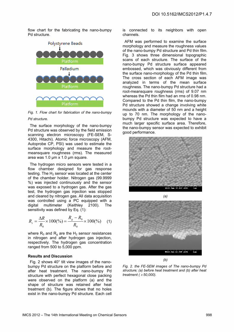
Results and Discussion Fig. 2 shows 40° tilt view images of the nano-
bumpy Pd structure on the platform before and after heat treatment. The nano-bumpy Pd structure with perfect hexagonal close packing were observed on the platform (a) and the shape of structure was retained after heat treatment (b). The figure shows that no holes exist in the nano-bumpy Pd structure. Each cell
is connected to its neighbors with open channels.
AFM was performed to examine the surface morphology and measure the roughness values of the nano-bumpy Pd structure and Pd thin film. Fig. 3 shows three dimensional topographic scans of each structure. The surface of the nano-bumpy Pd structure surface appeared embossed, which was obviously different from the surface nano-morphology of the Pd thin film. The cross section of each AFM image was analyzed in terms of the mean surface roughness. The nano-bumpy Pd structure had a root-meansquare roughness (rms) of 9.07 nm whereas the Pd thin film had an rms of 0.98 nm. Compared to the Pd thin film, the nano-bumpy Pd structure showed a change involving white mounds with a diameter of 50 nm and a height up to 70 nm. The morphology of the nano-bumpy Pd structure was expected to have a much larger specific surface area. Therefore, the nano-bumpy sensor was expected to exhibit good performance.
(a)
(b)
Fig. 2. the FE-SEM images of The nano-bumpy Pd structure; (a) before heat treatment and (b) after heat treatment (ⅹ50,000).
DOI 10.5162/IMCS2012/P1.4.7
IMCS 2012 – The 14th International Meeting on Chemical Sensors 998

(a)
(b)
Fig. 3. (a) Three dimensional AFM micrographs of the Pd thin film and (b) Three dimensional AFM micrographs of the nano-bumpy Pd structure.
According to a previous study [9], with respect to the Pd thin film sensor, the optimal heater voltage was 4.0 V and the sensitivity and response time (defined as that required for 90 % of the full signal change) for a hydrogen gas injection of 2000 ppm were 0.638 % and 27 seconds, respectively. Fig. 4 shows the Rs and response time of the Pd nano-bumpy sensor at various heater voltages at a hydrogen gas injection of 2000 ppm. After applying heater voltages of 0 ~ 5 V, the Rs of the H2 sensor was 1.09, 0.97, 0.82, 0.75, 0.65 and 0.53 % and the response time was 96, 84, 56, 90, 98 and 102 seconds, respectively. With increasing applied voltage, the Rs of the nano-bumpy sensor decreased and the response time was shorter than that of other heater voltages at a heater voltage of 2 V (i.e. 70°C). Because the surface area is improved at the nano-bumpy sensor, the nano-bumpy sensor at 0 V showed higher sensitivity and a longer response time than the thin film sensor. With increasing operating temperature of the nano-bumpy sensor, the adsorption energy decreased and the adsorption rate increased. Therefore, the response time became fast. In addition, the desorption energy also decreased with increasing operating temperature and the desorption rate was efficiently high at above 2 V. Because the adsorption and desorption of hydrogen on a Pd surface at high temperatures (> 2 V) occurs at the same time, the response time would be expected to be longer than at 2 V. Therefore, the optimal heater voltage in the nano-bumpy sensor can be selected in the range of 0-2.0 V, compensating for the sensitivity with response time.
Fig. 4. The sensitivity and response time of nano-bumpy sensor at various heater voltages at 2,000 ppm hydrogen gas injection.
Fig. 5 shows the sensitivity of the hydrogen sensors at various hydrogen gas concentrations. At hydrogen gas concentrations of 500, 1,000, 2,000 and 5,000 ppm, the sensitivity of the thin film sensor was 0.271, 0.379, 0.638 and 1.157 %, respectively and that of the nano-bumpy sensor was 0.491, 0.736, 1.045 and 1.764 %, respectively, which demonstrates improved sensitivity with increasing hydrogen gas concentration. The sensitivity of the nano-bumpy sensor was better than the thin film sensor due to very high surface-to-volume ratio of the nano-bumpy Pd structure. The increased sensitivity was attributed to the increased active area between the hydrogen gas molecules and nano-bumpy Pd surface.
Fig. 5. The sensitivity of the hydrogen sensors at hydrogen gas concentrations.
Conclusions Highly sensitive hydrogen gas sensors were
fabricated. A 50 nm-thick Pd thin film was deposited by R.F. magnetron sputtering. FE-SEM and AFM confirmed the nano-bumpy Pd structure. The sensitivity of the hydrogen sensor was measured at hydrogen gas concentration of 500 ppm to 5,000 ppm. At a hydrogen gas concentration of 2,000, the sensitivity of the Pd thin film sensor and Pd
DOI 10.5162/IMCS2012/P1.4.7
IMCS 2012 – The 14th International Meeting on Chemical Sensors 999

nano-bumpy sensor was 0.638 and 0.745, respectively. The sensitivity of the nano-bumpy sensor was better than that of the thin film sensor due to very high surface-to-volume ratio of the nano-bumpy Pd structure. The gas sensing characteristics of the hydrogen sensors was positively correlated with the hydrogen concentration.
Acknowledgements This research was supported by a grant from
the Fundamental R&D Program for Core Technology of Materials funded by the Ministry of Knowledge Economy, Republic of Korea, in 2008.
References [1] H. Görgün, M. Arcak, S. Varigonda, S.A. Bortoff,
Int. J. Hydrogen Energy 30, 447-457 (2005); doi: 10.1016/j.ijhydene.2004.10.024
[2] E. Sennik, Z. Colak, N. Kilinc, Z.Z. Ozturk, Int. J. Hydrogen Energy 35, 4420-4427 (2010); doi: 10.1016/j.ijhydene.2010.01.100
[3] K. Skucha, Z.Y. Fan, K. Jeon, A. Javey, B. Boser, Sens. Actuators B: Chem. 145, 232-238 (2010); doi: 10.1016/j.snb.2009.11.067
[4] D. Monzon-Hernandez, D. Luna-Moreno, D. Martinez-Escobar, Sens. Actuators B: Chem. 136, 562-566 (2009); doi: 10.1016/j.snb.2008.12.019
[5] F. Yang, S.C. Kung, D.K. Taggart, R.M. Penner, Sens. Lett. 8, 534-538 (2010); doi: 10.1166/sl.2010.1307
[6] F. Yang, D.K. Taggart, R.M. Penner, Nano Lett. 9, 2177-2182 (2009); doi: 10.1021/nl9008474 CCC
[7] N. Tasaltin, S. Ozturk, N. Kilinc, Z.Z. Ozturk, Appl. Phys. A: Mater. 97, 745-750 (2009); doi: 10.1007/s00339-009-5440-7
[8] E. Sennik, N. Kilinc, Z.Z. Ozturk, J. Appl. Phys. 108, 054317 (2010); doi: 10.1063/1.3481430
[9] J. H. Yoon,B.J. Kim,J.S. Kim, Mater. Chem. Phys., in press (2012); doi: 10.1016/j.matchemphys.2012.02.002
DOI 10.5162/IMCS2012/P1.4.7
IMCS 2012 – The 14th International Meeting on Chemical Sensors 1000