september 2011 precision micropower … · slos746a –september 2011–revised september 2011...
TRANSCRIPT
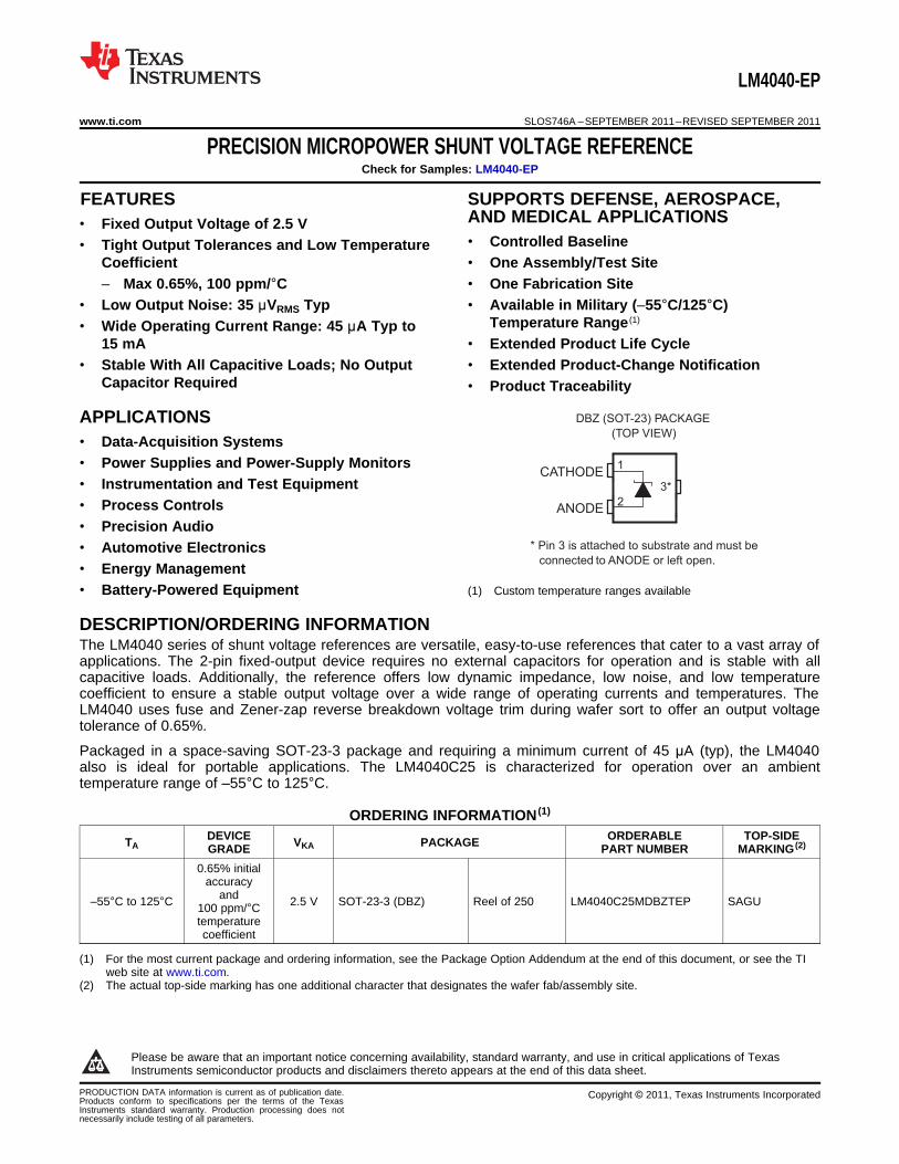
* Pin 3 is attached to substrate and must be
connected to ANODE or left open.
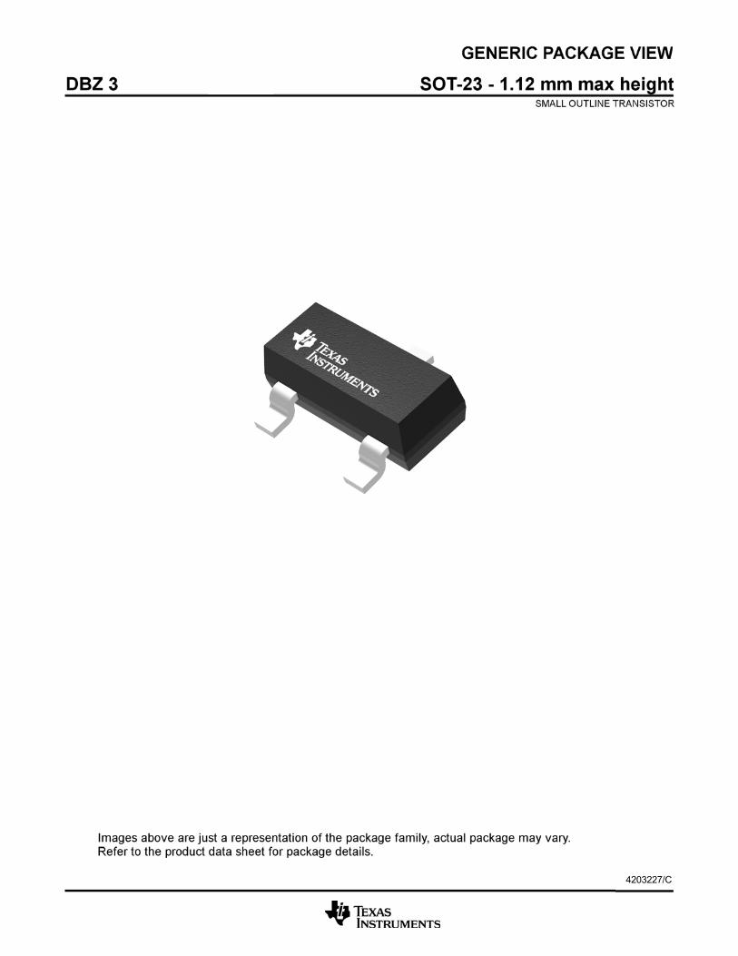
DBZ (SOT-23) PACKAGE
(TOP VIEW)
CATHODE
ANODE
1
2
3*
LM4040-EP
www.ti.com SLOS746A –SEPTEMBER 2011–REVISED SEPTEMBER 2011
PRECISION MICROPOWER SHUNT VOLTAGE REFERENCECheck for Samples: LM4040-EP
1FEATURES SUPPORTS DEFENSE, AEROSPACE,AND MEDICAL APPLICATIONS• Fixed Output Voltage of 2.5 V• Controlled Baseline• Tight Output Tolerances and Low Temperature
Coefficient • One Assembly/Test Site– Max 0.65%, 100 ppm/°C • One Fabrication Site
• Low Output Noise: 35 μVRMS Typ • Available in Military (–55°C/125°C)Temperature Range (1)• Wide Operating Current Range: 45 μA Typ to
15 mA • Extended Product Life Cycle• Stable With All Capacitive Loads; No Output • Extended Product-Change Notification
Capacitor Required • Product Traceability
APPLICATIONS• Data-Acquisition Systems• Power Supplies and Power-Supply Monitors• Instrumentation and Test Equipment• Process Controls• Precision Audio• Automotive Electronics• Energy Management• Battery-Powered Equipment (1) Custom temperature ranges available
DESCRIPTION/ORDERING INFORMATIONThe LM4040 series of shunt voltage references are versatile, easy-to-use references that cater to a vast array ofapplications. The 2-pin fixed-output device requires no external capacitors for operation and is stable with allcapacitive loads. Additionally, the reference offers low dynamic impedance, low noise, and low temperaturecoefficient to ensure a stable output voltage over a wide range of operating currents and temperatures. TheLM4040 uses fuse and Zener-zap reverse breakdown voltage trim during wafer sort to offer an output voltagetolerance of 0.65%.
Packaged in a space-saving SOT-23-3 package and requiring a minimum current of 45 μA (typ), the LM4040also is ideal for portable applications. The LM4040C25 is characterized for operation over an ambienttemperature range of –55°C to 125°C.
ORDERING INFORMATION (1)
DEVICE ORDERABLE TOP-SIDETA VKA PACKAGEGRADE PART NUMBER MARKING (2)
0.65% initialaccuracy
and–55°C to 125°C 2.5 V SOT-23-3 (DBZ) Reel of 250 LM4040C25MDBZTEP SAGU100 ppm/°Ctemperaturecoefficient
(1) For the most current package and ordering information, see the Package Option Addendum at the end of this document, or see the TIweb site at www.ti.com.
(2) The actual top-side marking has one additional character that designates the wafer fab/assembly site.
1
Please be aware that an important notice concerning availability, standard warranty, and use in critical applications of TexasInstruments semiconductor products and disclaimers thereto appears at the end of this data sheet.
PRODUCTION DATA information is current as of publication date. Copyright © 2011, Texas Instruments IncorporatedProducts conform to specifications per the terms of the TexasInstruments standard warranty. Production processing does notnecessarily include testing of all parameters.
CATHODE
ANODE
_+
LM4040-EP
SLOS746A –SEPTEMBER 2011–REVISED SEPTEMBER 2011 www.ti.com
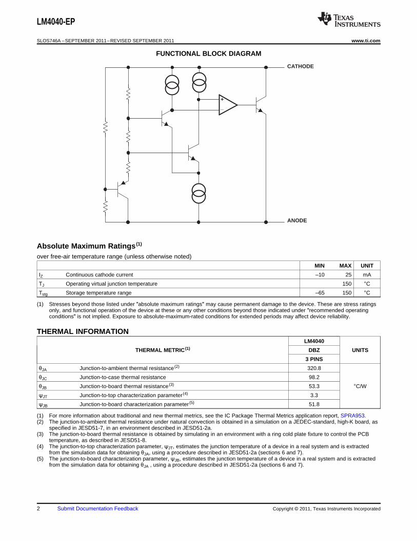
FUNCTIONAL BLOCK DIAGRAM
Absolute Maximum Ratings (1)
over free-air temperature range (unless otherwise noted)
MIN MAX UNIT
IZ Continuous cathode current –10 25 mA
TJ Operating virtual junction temperature 150 °CTstg Storage temperature range –65 150 °C
(1) Stresses beyond those listed under "absolute maximum ratings" may cause permanent damage to the device. These are stress ratingsonly, and functional operation of the device at these or any other conditions beyond those indicated under "recommended operatingconditions" is not implied. Exposure to absolute-maximum-rated conditions for extended periods may affect device reliability.
THERMAL INFORMATIONLM4040
THERMAL METRIC (1) DBZ UNITS
3 PINS
θJA Junction-to-ambient thermal resistance (2) 320.8
θJC Junction-to-case thermal resistance 98.2
θJB Junction-to-board thermal resistance (3) 53.3 °C/W
ψJT Junction-to-top characterization parameter (4) 3.3
ψJB Junction-to-board characterization parameter (5) 51.8
(1) For more information about traditional and new thermal metrics, see the IC Package Thermal Metrics application report, SPRA953.(2) The junction-to-ambient thermal resistance under natural convection is obtained in a simulation on a JEDEC-standard, high-K board, as
specified in JESD51-7, in an environment described in JESD51-2a.(3) The junction-to-board thermal resistance is obtained by simulating in an environment with a ring cold plate fixture to control the PCB
temperature, as described in JESD51-8.(4) The junction-to-top characterization parameter, ψJT, estimates the junction temperature of a device in a real system and is extracted
from the simulation data for obtaining θJA, using a procedure described in JESD51-2a (sections 6 and 7).(5) The junction-to-board characterization parameter, ψJB, estimates the junction temperature of a device in a real system and is extracted
from the simulation data for obtaining θJA , using a procedure described in JESD51-2a (sections 6 and 7).
2 Submit Documentation Feedback Copyright © 2011, Texas Instruments Incorporated
VZIZ
LM4040-EP
www.ti.com SLOS746A –SEPTEMBER 2011–REVISED SEPTEMBER 2011
Recommended Operating ConditionsMIN MAX UNIT
IZ Cathode current See (1) 15 mA
TA Free-air temperature –55 125 °C
(1) See parametric tables
Electrical Characteristicsat extended temperature range, full-range TA = –55°C to 125°C (unless otherwise noted)
PARAMETER TEST CONDITIONS TA MIN TYP MAX UNIT
VZ Reverse breakdown voltage IZ = 100 μA 25°C 2.5 V
25°C –16 16Reverse breakdown voltageΔVZ IZ = 100 μA mVtolerance Full range –42 42
25°C 45 75IZ,min Minimum cathode current μA
Full range 82
IZ = 10 mA 25°C ±20
25°C ±15Average temperature coefficient ofαVZ IZ = 1 mA ppm/°Creverse breakdown voltage Full range ±100
IZ = 100 μA 25°C ±15
25°C 0.3 0.8IZ,min < IZ < 1 mA
Full range 1.1Reverse breakdown voltage change mVwith cathode current change 25°C 2.5 61 mA < IZ < 15 mA
Full range 9
IZ = 1 mA, f = 120 Hz,ZZ Reverse dynamic impedance 25°C 0.3 ΩIAC = 0.1 IZ
IZ = 100 μA,eN Wideband noise 25°C 35 μVRMS10 Hz ≤ f ≤ 10 kHz
t = 1000 h,Long-term stability of reverse TA = 25°C ± 0.1°C, 120 ppmbreakdown voltage IZ = 100 μA
VHYST Thermal hysteresis (1) ΔTA = –55°C to 125°C 0.08 %
(1) Thermal hysteresis is defined as VZ,25°C (after cycling to –55°C) – VZ,25°C (after cycling to 125°C).
Copyright © 2011, Texas Instruments Incorporated Submit Documentation Feedback 3
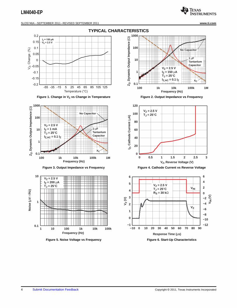
Temperature (°C)
VZ, C
hange
(%)
-0.2
-0.15
-0.1
-0.05
0
0.05
0.1
0.15
0.2
-55 -35 -15 5 25 45 65 85 105 125
I = 150 µA
V = 2.5 VZ
Z
100 1k 1M10k 100kFrequency (Hz)
ZZ,
Dyn
amic
Ou
tpu
t Im
ped
ance
(Ω) 1000
100
10
1
0.1
VZ = 2.5 VIZ = 150 µATJ = 25°CIZ,AC = 0.1 IZ XC
No Capacitor
1 µFTantanlumCapacitor
100 1k 1M10k 100kFrequency (Hz)
ZZ,
Dyn
amic
Out
put I
mpe
danc
e (
Ω) 1000
100
10
1
0.1
VZ = 2.5 VIZ = 1 mATJ = 25°CIZ,AC = 0.1 IZ
XC
No Capacitor
1-µFTantanlumCapacitor
0
20
40
60
80
100
120
0.0 0.5 1.0 1.5 2.0 2.5 3.0
VZ, Reverse Voltage (V)
I Z, C
ath
od
e C
urr
ent
µA)
VZ = 2.5 VTJ = 25°C
0 1 2.51.5 20.5 3
1 100 100k1k 10kFrequency (Hz)
No
ise
(µVH
z)
10
1
0.110
VZ = 2.5 VIZ = 200 µATJ = 25°C
−1
0
1
2
3
4
5
6
−10 0 10 20 30 40 50 60 70 80 90
VZ
(V)
VZ = 2.5 VTJ = 25°CRS = 30 kΩ
Response T ime (µs)
VIN
VZV
IN (V
)
6
4
2
0
−2
−4
−6
−8
−10
−12
LM4040-EP
SLOS746A –SEPTEMBER 2011–REVISED SEPTEMBER 2011 www.ti.com
TYPICAL CHARACTERISTICS
Figure 1. Change in VZ vs Change in Temperature Figure 2. Output Impedance vs Frequency
Figure 3. Output Impedance vs Frequency Figure 4. Cathode Current vs Reverse Voltage
Figure 5. Noise Voltage vs Frequency Figure 6. Start-Up Characteristics
4 Submit Documentation Feedback Copyright © 2011, Texas Instruments Incorporated
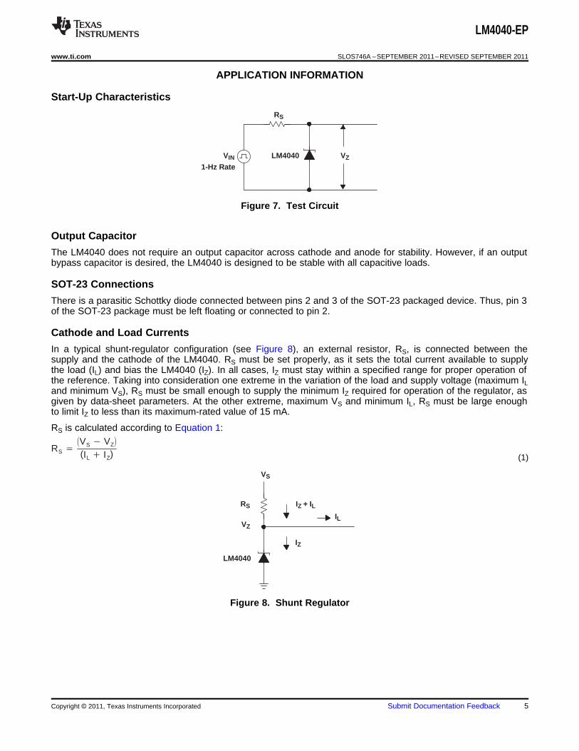
1-Hz Rate
VZLM4040
RS
VIN
RS VS VZ
(IL IZ)
LM4040
IZ + ILIL
IZ
VS
VZ
RS
LM4040-EP
www.ti.com SLOS746A –SEPTEMBER 2011–REVISED SEPTEMBER 2011
APPLICATION INFORMATION
Start-Up Characteristics
Figure 7. Test Circuit
Output Capacitor
The LM4040 does not require an output capacitor across cathode and anode for stability. However, if an outputbypass capacitor is desired, the LM4040 is designed to be stable with all capacitive loads.
SOT-23 Connections
There is a parasitic Schottky diode connected between pins 2 and 3 of the SOT-23 packaged device. Thus, pin 3of the SOT-23 package must be left floating or connected to pin 2.
Cathode and Load Currents
In a typical shunt-regulator configuration (see Figure 8), an external resistor, RS, is connected between thesupply and the cathode of the LM4040. RS must be set properly, as it sets the total current available to supplythe load (IL) and bias the LM4040 (IZ). In all cases, IZ must stay within a specified range for proper operation ofthe reference. Taking into consideration one extreme in the variation of the load and supply voltage (maximum ILand minimum VS), RS must be small enough to supply the minimum IZ required for operation of the regulator, asgiven by data-sheet parameters. At the other extreme, maximum VS and minimum IL, RS must be large enoughto limit IZ to less than its maximum-rated value of 15 mA.
RS is calculated according to Equation 1:
(1)
Figure 8. Shunt Regulator
Copyright © 2011, Texas Instruments Incorporated Submit Documentation Feedback 5
PACKAGE OPTION ADDENDUM
www.ti.com 31-May-2014
Addendum-Page 1
PACKAGING INFORMATION
Orderable Device Status(1)
Package Type PackageDrawing
Pins PackageQty
Eco Plan(2)
Lead/Ball Finish(6)
MSL Peak Temp(3)
Op Temp (°C) Device Marking(4/5)
Samples
LM4040C25MDBZTEP ACTIVE SOT-23 DBZ 3 250 Green (RoHS& no Sb/Br)
CU NIPDAU Level-1-260C-UNLIM -55 to 125 SAGU
V62/11615-01XB ACTIVE SOT-23 DBZ 3 250 Green (RoHS& no Sb/Br)
CU NIPDAU Level-1-260C-UNLIM -55 to 125 SAGU
(1) The marketing status values are defined as follows:ACTIVE: Product device recommended for new designs.LIFEBUY: TI has announced that the device will be discontinued, and a lifetime-buy period is in effect.NRND: Not recommended for new designs. Device is in production to support existing customers, but TI does not recommend using this part in a new design.PREVIEW: Device has been announced but is not in production. Samples may or may not be available.OBSOLETE: TI has discontinued the production of the device.
(2) Eco Plan - The planned eco-friendly classification: Pb-Free (RoHS), Pb-Free (RoHS Exempt), or Green (RoHS & no Sb/Br) - please check http://www.ti.com/productcontent for the latest availabilityinformation and additional product content details.TBD: The Pb-Free/Green conversion plan has not been defined.Pb-Free (RoHS): TI's terms "Lead-Free" or "Pb-Free" mean semiconductor products that are compatible with the current RoHS requirements for all 6 substances, including the requirement thatlead not exceed 0.1% by weight in homogeneous materials. Where designed to be soldered at high temperatures, TI Pb-Free products are suitable for use in specified lead-free processes.Pb-Free (RoHS Exempt): This component has a RoHS exemption for either 1) lead-based flip-chip solder bumps used between the die and package, or 2) lead-based die adhesive used betweenthe die and leadframe. The component is otherwise considered Pb-Free (RoHS compatible) as defined above.Green (RoHS & no Sb/Br): TI defines "Green" to mean Pb-Free (RoHS compatible), and free of Bromine (Br) and Antimony (Sb) based flame retardants (Br or Sb do not exceed 0.1% by weightin homogeneous material)
(3) MSL, Peak Temp. - The Moisture Sensitivity Level rating according to the JEDEC industry standard classifications, and peak solder temperature.
(4) There may be additional marking, which relates to the logo, the lot trace code information, or the environmental category on the device.
(5) Multiple Device Markings will be inside parentheses. Only one Device Marking contained in parentheses and separated by a "~" will appear on a device. If a line is indented then it is a continuationof the previous line and the two combined represent the entire Device Marking for that device.
(6) Lead/Ball Finish - Orderable Devices may have multiple material finish options. Finish options are separated by a vertical ruled line. Lead/Ball Finish values may wrap to two lines if the finishvalue exceeds the maximum column width.
Important Information and Disclaimer:The information provided on this page represents TI's knowledge and belief as of the date that it is provided. TI bases its knowledge and belief on informationprovided by third parties, and makes no representation or warranty as to the accuracy of such information. Efforts are underway to better integrate information from third parties. TI has taken andcontinues to take reasonable steps to provide representative and accurate information but may not have conducted destructive testing or chemical analysis on incoming materials and chemicals.TI and TI suppliers consider certain information to be proprietary, and thus CAS numbers and other limited information may not be available for release.
PACKAGE OPTION ADDENDUM
www.ti.com 31-May-2014
Addendum-Page 2
In no event shall TI's liability arising out of such information exceed the total purchase price of the TI part(s) at issue in this document sold by TI to Customer on an annual basis.
OTHER QUALIFIED VERSIONS OF LM4040C25-EP :
• Catalog: LM4040C25
NOTE: Qualified Version Definitions:
• Catalog - TI's standard catalog product
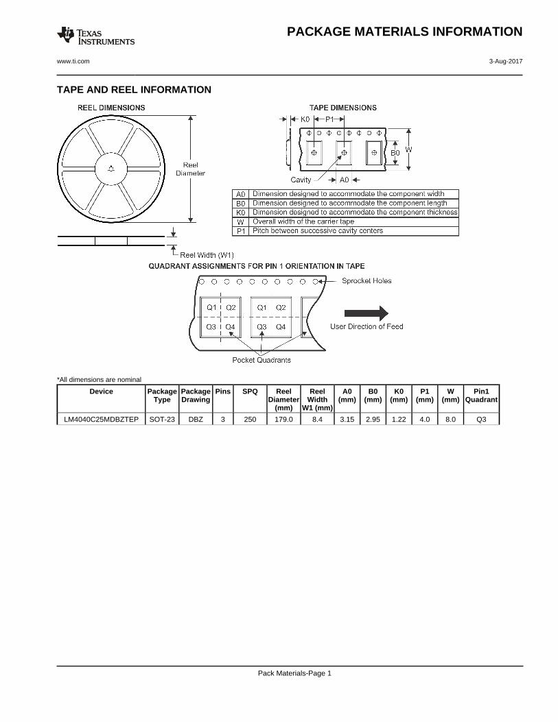
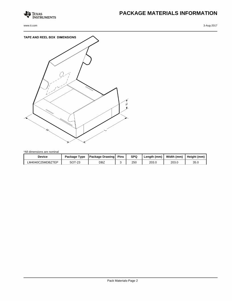
TAPE AND REEL INFORMATION
*All dimensions are nominal
Device PackageType
PackageDrawing
Pins SPQ ReelDiameter
(mm)
ReelWidth
W1 (mm)
A0(mm)
B0(mm)
K0(mm)
P1(mm)
W(mm)
Pin1Quadrant
LM4040C25MDBZTEP SOT-23 DBZ 3 250 179.0 8.4 3.15 2.95 1.22 4.0 8.0 Q3
PACKAGE MATERIALS INFORMATION
www.ti.com 3-Aug-2017
Pack Materials-Page 1
*All dimensions are nominal
Device Package Type Package Drawing Pins SPQ Length (mm) Width (mm) Height (mm)
LM4040C25MDBZTEP SOT-23 DBZ 3 250 203.0 203.0 35.0
PACKAGE MATERIALS INFORMATION
www.ti.com 3-Aug-2017
Pack Materials-Page 2
4203227/C
www.ti.com
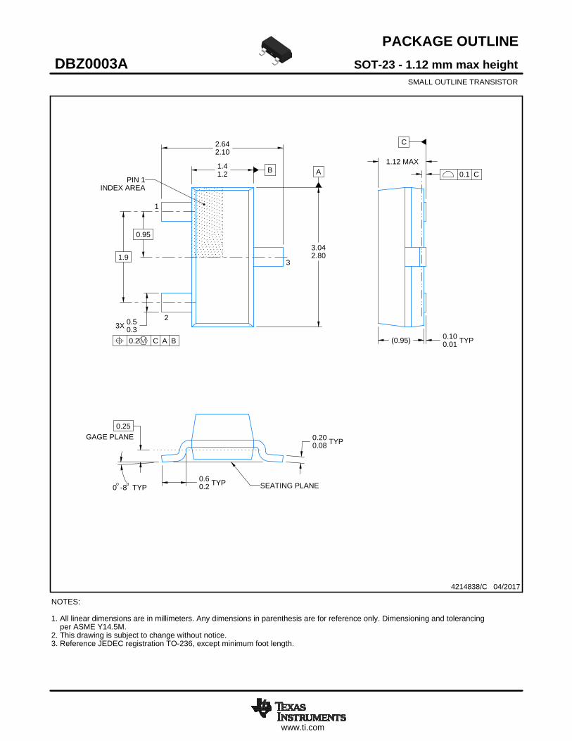
PACKAGE OUTLINE
C
TYP0.200.08
0.25
2.642.10
1.12 MAX
TYP0.100.01
3X 0.50.3
TYP0.60.2
1.9
0.95
TYP-80
A
3.042.80
B1.41.2
(0.95)
SOT-23 - 1.12 mm max heightDBZ0003ASMALL OUTLINE TRANSISTOR
4214838/C 04/2017
NOTES: 1. All linear dimensions are in millimeters. Any dimensions in parenthesis are for reference only. Dimensioning and tolerancing per ASME Y14.5M.2. This drawing is subject to change without notice.3. Reference JEDEC registration TO-236, except minimum foot length.
0.2 C A B
1
3
2
INDEX AREAPIN 1
GAGE PLANE
SEATING PLANE
0.1 C
SCALE 4.000
www.ti.com
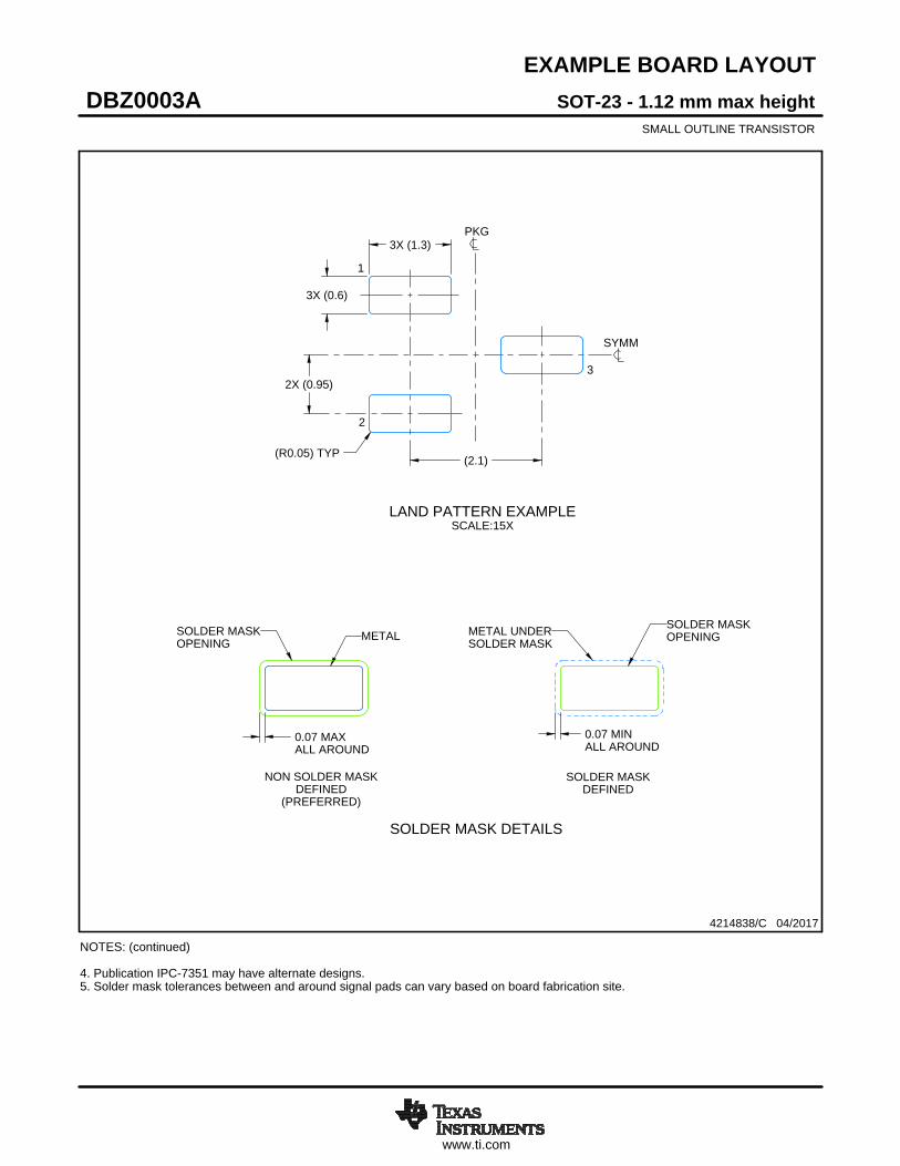
EXAMPLE BOARD LAYOUT
0.07 MAXALL AROUND
0.07 MINALL AROUND
3X (1.3)
3X (0.6)
(2.1)
2X (0.95)
(R0.05) TYP
4214838/C 04/2017
SOT-23 - 1.12 mm max heightDBZ0003ASMALL OUTLINE TRANSISTOR
NOTES: (continued) 4. Publication IPC-7351 may have alternate designs. 5. Solder mask tolerances between and around signal pads can vary based on board fabrication site.
SYMM
LAND PATTERN EXAMPLESCALE:15X
PKG
1
3
2
SOLDER MASKOPENINGMETAL UNDER
SOLDER MASK
SOLDER MASKDEFINED
METALSOLDER MASKOPENING
NON SOLDER MASKDEFINED
(PREFERRED)
SOLDER MASK DETAILS
www.ti.com
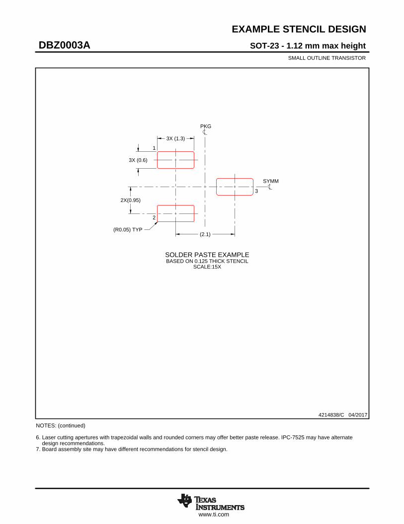
EXAMPLE STENCIL DESIGN
(2.1)
2X(0.95)
3X (1.3)
3X (0.6)
(R0.05) TYP
SOT-23 - 1.12 mm max heightDBZ0003ASMALL OUTLINE TRANSISTOR
4214838/C 04/2017
NOTES: (continued) 6. Laser cutting apertures with trapezoidal walls and rounded corners may offer better paste release. IPC-7525 may have alternate design recommendations. 7. Board assembly site may have different recommendations for stencil design.
SOLDER PASTE EXAMPLEBASED ON 0.125 THICK STENCIL
SCALE:15X
SYMM
PKG
1
3
2
IMPORTANT NOTICE
Texas Instruments Incorporated (TI) reserves the right to make corrections, enhancements, improvements and other changes to itssemiconductor products and services per JESD46, latest issue, and to discontinue any product or service per JESD48, latest issue. Buyersshould obtain the latest relevant information before placing orders and should verify that such information is current and complete.TI’s published terms of sale for semiconductor products (http://www.ti.com/sc/docs/stdterms.htm) apply to the sale of packaged integratedcircuit products that TI has qualified and released to market. Additional terms may apply to the use or sale of other types of TI products andservices.Reproduction of significant portions of TI information in TI data sheets is permissible only if reproduction is without alteration and isaccompanied by all associated warranties, conditions, limitations, and notices. TI is not responsible or liable for such reproduceddocumentation. Information of third parties may be subject to additional restrictions. Resale of TI products or services with statementsdifferent from or beyond the parameters stated by TI for that product or service voids all express and any implied warranties for theassociated TI product or service and is an unfair and deceptive business practice. TI is not responsible or liable for any such statements.Buyers and others who are developing systems that incorporate TI products (collectively, “Designers”) understand and agree that Designersremain responsible for using their independent analysis, evaluation and judgment in designing their applications and that Designers havefull and exclusive responsibility to assure the safety of Designers' applications and compliance of their applications (and of all TI productsused in or for Designers’ applications) with all applicable regulations, laws and other applicable requirements. Designer represents that, withrespect to their applications, Designer has all the necessary expertise to create and implement safeguards that (1) anticipate dangerousconsequences of failures, (2) monitor failures and their consequences, and (3) lessen the likelihood of failures that might cause harm andtake appropriate actions. Designer agrees that prior to using or distributing any applications that include TI products, Designer willthoroughly test such applications and the functionality of such TI products as used in such applications.TI’s provision of technical, application or other design advice, quality characterization, reliability data or other services or information,including, but not limited to, reference designs and materials relating to evaluation modules, (collectively, “TI Resources”) are intended toassist designers who are developing applications that incorporate TI products; by downloading, accessing or using TI Resources in anyway, Designer (individually or, if Designer is acting on behalf of a company, Designer’s company) agrees to use any particular TI Resourcesolely for this purpose and subject to the terms of this Notice.TI’s provision of TI Resources does not expand or otherwise alter TI’s applicable published warranties or warranty disclaimers for TIproducts, and no additional obligations or liabilities arise from TI providing such TI Resources. TI reserves the right to make corrections,enhancements, improvements and other changes to its TI Resources. TI has not conducted any testing other than that specificallydescribed in the published documentation for a particular TI Resource.Designer is authorized to use, copy and modify any individual TI Resource only in connection with the development of applications thatinclude the TI product(s) identified in such TI Resource. NO OTHER LICENSE, EXPRESS OR IMPLIED, BY ESTOPPEL OR OTHERWISETO ANY OTHER TI INTELLECTUAL PROPERTY RIGHT, AND NO LICENSE TO ANY TECHNOLOGY OR INTELLECTUAL PROPERTYRIGHT OF TI OR ANY THIRD PARTY IS GRANTED HEREIN, including but not limited to any patent right, copyright, mask work right, orother intellectual property right relating to any combination, machine, or process in which TI products or services are used. Informationregarding or referencing third-party products or services does not constitute a license to use such products or services, or a warranty orendorsement thereof. Use of TI Resources may require a license from a third party under the patents or other intellectual property of thethird party, or a license from TI under the patents or other intellectual property of TI.TI RESOURCES ARE PROVIDED “AS IS” AND WITH ALL FAULTS. TI DISCLAIMS ALL OTHER WARRANTIES ORREPRESENTATIONS, EXPRESS OR IMPLIED, REGARDING RESOURCES OR USE THEREOF, INCLUDING BUT NOT LIMITED TOACCURACY OR COMPLETENESS, TITLE, ANY EPIDEMIC FAILURE WARRANTY AND ANY IMPLIED WARRANTIES OFMERCHANTABILITY, FITNESS FOR A PARTICULAR PURPOSE, AND NON-INFRINGEMENT OF ANY THIRD PARTY INTELLECTUALPROPERTY RIGHTS. TI SHALL NOT BE LIABLE FOR AND SHALL NOT DEFEND OR INDEMNIFY DESIGNER AGAINST ANY CLAIM,INCLUDING BUT NOT LIMITED TO ANY INFRINGEMENT CLAIM THAT RELATES TO OR IS BASED ON ANY COMBINATION OFPRODUCTS EVEN IF DESCRIBED IN TI RESOURCES OR OTHERWISE. IN NO EVENT SHALL TI BE LIABLE FOR ANY ACTUAL,DIRECT, SPECIAL, COLLATERAL, INDIRECT, PUNITIVE, INCIDENTAL, CONSEQUENTIAL OR EXEMPLARY DAMAGES INCONNECTION WITH OR ARISING OUT OF TI RESOURCES OR USE THEREOF, AND REGARDLESS OF WHETHER TI HAS BEENADVISED OF THE POSSIBILITY OF SUCH DAMAGES.Unless TI has explicitly designated an individual product as meeting the requirements of a particular industry standard (e.g., ISO/TS 16949and ISO 26262), TI is not responsible for any failure to meet such industry standard requirements.Where TI specifically promotes products as facilitating functional safety or as compliant with industry functional safety standards, suchproducts are intended to help enable customers to design and create their own applications that meet applicable functional safety standardsand requirements. Using products in an application does not by itself establish any safety features in the application. Designers mustensure compliance with safety-related requirements and standards applicable to their applications. Designer may not use any TI products inlife-critical medical equipment unless authorized officers of the parties have executed a special contract specifically governing such use.Life-critical medical equipment is medical equipment where failure of such equipment would cause serious bodily injury or death (e.g., lifesupport, pacemakers, defibrillators, heart pumps, neurostimulators, and implantables). Such equipment includes, without limitation, allmedical devices identified by the U.S. Food and Drug Administration as Class III devices and equivalent classifications outside the U.S.TI may expressly designate certain products as completing a particular qualification (e.g., Q100, Military Grade, or Enhanced Product).Designers agree that it has the necessary expertise to select the product with the appropriate qualification designation for their applicationsand that proper product selection is at Designers’ own risk. Designers are solely responsible for compliance with all legal and regulatoryrequirements in connection with such selection.Designer will fully indemnify TI and its representatives against any damages, costs, losses, and/or liabilities arising out of Designer’s non-compliance with the terms and provisions of this Notice.
Mailing Address: Texas Instruments, Post Office Box 655303, Dallas, Texas 75265Copyright © 2017, Texas Instruments Incorporated