sequential quantum dot cellular automata design and analysis using dynamic bayesian networks
TRANSCRIPT

University of South FloridaScholar Commons
Graduate Theses and Dissertations Graduate School
2008
Sequential quantum dot cellular automata designand analysis using Dynamic Bayesian NetworksPraveen VenkataramaniUniversity of South Florida
Follow this and additional works at: http://scholarcommons.usf.edu/etd
Part of the American Studies Commons
This Thesis is brought to you for free and open access by the Graduate School at Scholar Commons. It has been accepted for inclusion in GraduateTheses and Dissertations by an authorized administrator of Scholar Commons. For more information, please contact [email protected].
Scholar Commons CitationVenkataramani, Praveen, "Sequential quantum dot cellular automata design and analysis using Dynamic Bayesian Networks" (2008).Graduate Theses and Dissertations.http://scholarcommons.usf.edu/etd/545

Sequential Quantum-Dot Cellular Automata Design And Analysis Using Dynamic
Bayesian Networks
by
Praveen Venkataramani
A thesis submitted in partial fulfillment of the requirements for the degree of
Master of Electrical Engineering Department of Electrical Engineering
College of Engineering University of South Florida
Major Professor: Sannjukta Bhanja, Ph.D. Paris Wiley, Ph.D.
Wilfrido A. Moreno, Ph.D
Date of Approval: October 29, 2008
Keywords: probabilisitic modelling, qca, bayesian networks, quantum-dot cellular automata
© Copyright 2008 , Praveen Venkataramani

DEDICATION
To my parents.

ACKNOWLEDGEMENTS
I would like to take this opportunity to thank my professor Dr. Sanjukta Bhanja, who had
guided me through out my Graduate studies. She had helped me in learning different aspects
in research and to think as a researcher. Her valuable advice had helped me through out my
research work.
I thank Dr. Paris H.Wiley and Dr. Wilfredo A.Moreno for serving in my committee.
I thank my friends, family and colleagues who had given me support and had boosted my
confidence while it was low.

TABLE OF CONTENTS
LIST OF TABLES iii
LIST OF FIGURES iv
ABSTRACT vii
CHAPTER 1 INTRODUCTION 11.1 Motivation 21.2 Novelty of this Work 21.3 Contribution of this Work 4
1.3.1 Reliability Analysis 41.4 Organization of this Work 5
CHAPTER 2 QUANTUM-DOT CELLULAR AUTOMATA 62.1 History 62.2 Computing using QCA 8
2.2.1 Elements of QCA 92.2.1.1 Quantum Dots 9
2.2.2 QCA Cells 102.3 Mechanics of QCA 122.4 Logic Devices in QCA 16
2.4.1 Majority Logic Synthesis 172.5 Modeling QCA Designs 22
CHAPTER 3 DYNAMIC BAYESIAN MODEL 253.1 Introduction 253.2 Quantum Mechanical Probabilities 253.3 Overview of Bayesian Modeling 273.4 Dynamic Bayesian Model 30
3.4.1 Sequential Design of JK FF in QCA using DBN 333.4.2 Design of a Single Memory Cell in QCA using DBN 343.4.3 Design of s27 Sequential Benchmark Circuit in QCA using DBN 36
3.5 Estimated Posterior Importance Sampling 36
CHAPTER 4 VALIDATION OF DBN MODEL 41
i

CHAPTER 5 ANALYSIS OF SEQUENTIAL QCA CIRCUITS 445.1 Introduction 445.2 Temperature Characterization 455.3 Characterization Using Cell Dimensions 50
CHAPTER 6 CONCLUSION AND FUTURE WORKS 55
REFERENCES 56
ii

LIST OF TABLES
Table 4.1. Comparison of the Results obtained from QCADesginer and DBN Model,for JK FF at 2.0K using 18nm Cells 42
Table 4.2. Comparison of the Results obtained from QCADesginer and DBN Model,for RAM at 2.0K using 18nm Cells 42
Table 4.3. Comparison of the Results obtained from QCADesginer and DBN Model,for S27 at 2.0K using 18nm Cells 43
iii

LIST OF FIGURES
Figure 1.1. Table of Emerging Logic Devices 3
Figure 2.1. Unpolarized QCA Cell 11
Figure 2.2. QCA Cell and its Orientations 11
Figure 2.3. Binary Wire in QCA 11
Figure 2.4. Data Transfer in QCA 12
Figure 2.5. Infinite Well 14
Figure 2.6. Plot of the Energy Splitting between the Ground State and the First ExcitedState of an Electron undergoing Adiabatic Switching [1]. 15
Figure 2.7. Typical Adiabatic Clocking Operation in QCA [2]. 16
Figure 2.8. Majority Gate 17
Figure 2.9. Majority Computations 17
Figure 2.10. Inverter Design in QCA 18
Figure 2.11. AND Gate using Majority Function in QCA 18
Figure 2.12. OR Gate using Majority Function in QCA 18
Figure 2.13. NAND Gate using Majority Function in QCA 19
Figure 2.14. Full Adder Design in QCA 21
Figure 2.15. Majority Simplification of JK FF 22
Figure 2.16. JK Schematic from fig. 2.15. 22
Figure 2.17. JK FF Design using QCADesigner 23
Figure 3.1. A Small Bayesian Network 27
Figure 3.2. JK FF Designed in QCADesigner using 18nm Cells 32
Figure 3.3. JK FF Unraveled for two Time Slices using DBN 33
iv

Figure 3.4. Schematic of RAM 34
Figure 3.5. RAM Proposed in citeWalus03 35
Figure 3.6. RAM Designed using DBN 35
Figure 3.7. Schematic of s27 Sequential Benchmark Circuit 36
Figure 3.8. s27 Sequential Benchmark Circuit 37
Figure 3.9. s27 unraveled for two Time Slices using DBN 38
Figure 5.1. Results for Output Polarization Versus Time t at Different Temperaturesfor JK FF Circuit. 45
Figure 5.2. Results for Loop Polarization Versus Time t at Different Temperatures forRAM [3] Circuit During Write Mode (R/W=0). 46
Figure 5.3. Results for Loop Polarization versus Time t, when Input=0 and the Valuein the Feedback=1 at Different Temperatures for RAM [3] Circuit DuringRead Mode (R/W=1). 47
Figure 5.4. Results for Loop Polarization versus Time t, when Input=1 and the Valuein the Feedback=0 at Different Temperatures for RAM [3] Circuit DuringRead Mode (R/W=1). 47
Figure 5.5. Results For Output Polarization Versus Time t for the Inputs IN0=1 IN1=1IN2=1 IN3=1at Different Temperatures for S27 Benchmark Circuit 49
Figure 5.6. Results For Output Polarization Versus Time t for the Inputs IN0=1 IN1=0IN2=0 IN3=1at Different Temperatures for S27 Benchmark Circuit 49
Figure 5.7. Results with Output Polarization versus Time t at Different Cell Dimen-sions for JK FF Circuit 50
Figure 5.8. Results with Loop Polarization versus Time t at Different Cell Dimensionsfor RAM Circuit During Write Mode (R/W=0). 51
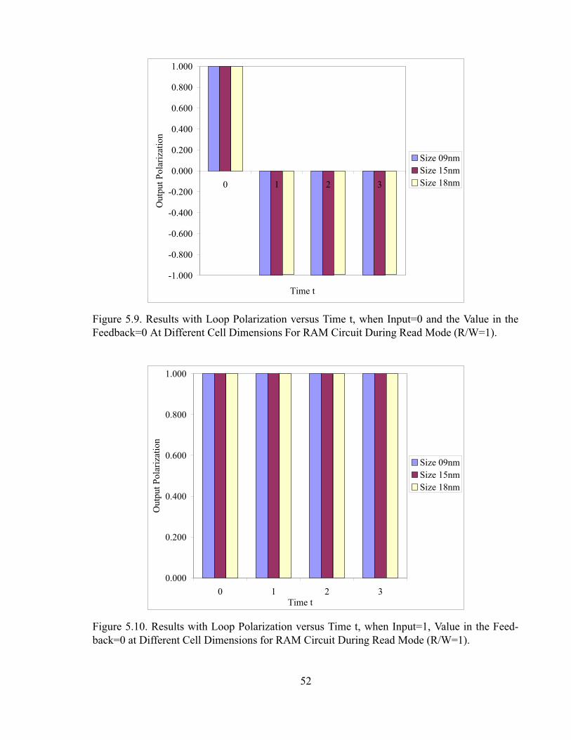
Figure 5.9. Results with Loop Polarization versus Time t, when Input=0 and the Valuein the Feedback=0 At Different Cell Dimensions For RAM Circuit DuringRead Mode (R/W=1). 52
Figure 5.10. Results with Loop Polarization versus Time t, when Input=1, Value in theFeedback=0 at Different Cell Dimensions for RAM Circuit During ReadMode (R/W=1). 52
Figure 5.11. Results with Output Polarization versus Time t, for the Inputs IN0=1 IN1=1IN2=1 IN3=1, at Different Cell Dimensions For S27 Benchmark Circuit 53
v

Figure 5.12. Results with Output Polarization versus Time t, for the Inputs IN0=1 IN1=0IN2=0 IN3=1, at Different Cell Dimensions for S27 Benchmark Circuit 53
vi

SEQUENTIAL QUANTUM DOT CELLULAR AUTOMATA DESIGN AND ANALYSISUSING DYNAMIC BAYESIAN NETWORKS
Praveen Venkataramani
ABSTRACT
The increasing need for low power and stunningly fast devices in Complementary Metal
Oxide Semiconductor Very large Scale Integration (CMOS VLSI) circuits, directs the stream
towards scaling of the same. However scaling at sub-micro level and nano level pose quantum
mechanical effects and thereby limits further scaling of CMOS circuits. Researchers look into
new aspects in nano regime that could effectively resolve this quandary. One such technology
that looks promising at nano-level is the quantum dot cellular automata (QCA). The basic op-
eration of QCA is based on transfer of charge rather than the electrons itself. The wave nature
of these electrons and their uncertainty in device operation demands a probabilistic approach to
study their operation.
The data is assigned to a QCA cell by positioning two electrons into four quantum dots.
However the site in which the electrons settles is uncertain and depends on various factors. In an
ideal state, the electrons position themselves diagonal to each other, through columbic repulsion,
to a low energy state. The quantum cell is said to be polarized to +1 or -1, based on the alignment
of the electrons.
In this thesis, we put forth a probabilistic model to design sequential QCA in Bayesian
networks. The timing constraints inherent in sequential circuits due to the feedback path, makes
it difficult to assign clock zones in a way that the outputs arrive at the same time instant. Hence
designing circuits that have many sequential elements is time consuming. The model presented
in this paper is fast and could be used to design sequential QCA circuits without the need to
vii

align the clock zones. One of the major advantages of our model lies in its ability to accurately
capture the polarization of each cell of the sequential QCA circuits.
We discuss the architecture of some of the basic sequential circuits such as J-K flip flop
(FF), RAM memory cell and s27 benchmark circuit designed in QCADesigner. We analyze
the circuits using a state-of-art Dynamic Bayesian Networks (DBN). To our knowledge this is
the first time sequential circuits are analyzed using DBN. For the first time, Estimated Posterior
Importance Sampling Algorithm (EPIS) is used to determine the probabilistic values, to study the
effect due to variations in physical dimension and operating temperature on output polarization
in QCA circuits.
viii

CHAPTER 1
INTRODUCTION
Transistors have been the fundamental device in almost all of today’s technologies. Gordon
Moore, co-founder of Intel Corporation, observed in early 1960’s that, the number of transistors
that could be inexpensively embedded in a specific area on a chip would increase exponentially
and double ever two years. This has been the challenge in transistor technology ever since. In-
dustries have linked every measure of device capabilities with this law. Transistors have evolved
through many levels of technology to the current and most widely used complementary metal
oxide semiconductor technology (CMOS). Semiconductor industries have used this technology
to crowd devices like microprocessors with billions of transistors today. Even though they have
been able to keep up with Moore’s law by shrinking the size of transistors from microns to sub-
microns and now to nano levels, researches have shown a limitation in the device operation at
such small sizes. This is mainly due to the intervention of quantum mechanical properties of
electrons at such miniscule sizes. It produced many undesired effects in device operation, such
as electron tunneling and power dissipation, which hindered further scaling of integrated circuits.
However industries still strive to keep Moore’s law true by reducing device sizes to nanometer
level while also looking into alternatives that could aid the high speed operation without the
problems experienced at sub nano level CMOS technologies. Now researchers across the world
have been proposing novel methods to satisfy the ever growing need for high speed devices and
have started to look beyond CMOS, into the properties of the electrons.
1

1.1 Motivation
It is clear from the pacing technological growth that nano-scale devices are already in pro-
duction. This is evident from the new Intel processors that use 32nm logic technology to design
SRAM with 1.9 billion transistors [4]. However designing and fabricating CMOS at nano level
comes with a cost. Issues related to oxide thickness, power dissipation, and thermal reliability
arises to question. So industries are in search for new materials and designs that could aid the
scaling of CMOS, but they are also well aware that CMOS technology could be continued only
for a decade [5]. Some of the emerging alternatives include carbon nanotubes, spintronics, spin-
valves etc [5]. Figure 1.1. show the emerging logic devices and along with their performance
parameters.
These circuits have device sizes near atomic and molecular dimensions. At such small sizes
the quantum mechanical effects are more dominant. Quantum-dot cellular automation (QCA) is
one such technology that promises the future of nano-technologies. QCA exploits the quandary
of device-device interaction that exists in CMOS scaling at nano-level, by using device inter-
actions for data propagation. Designing such circuits require a new design methodology that
could help to control the direction of propagation of data. The upper hand of QCA devices over
conventional CMOS circuits, apart from the one put forth above are, the absence of metallic
interconnects which is the main source of IR losses, the absence of electron flow for charge
transfer and of course its extreme low power consumption.
1.2 Novelty of this Work
Researchers have developed several models for defect characterization and design to mini-
mize the uncertainty of proper circuit operation. This uncertainty of the circuit aids in developing
a probabilistic model for analysis. One such model is the Bayesian network (BN) modeling [6],
which exploits the causal relationships in clocked QCA circuits to obtain a model with low
complexity. It is based on density matrix formulations and also takes the dependencies induced
2

Figure 1.1. Table of Emerging Logic Devices
by clocking of cells. One of the many interesting features of BN is that it not only captures
the dependencies existing between two QCA cells, but can also be used to conduct steady state
operations without the need for temporal computation of quantum mechanical equations.
Many circuits have been designed and analyzed using this model. Mostly the circuits are
combinational in nature, and were analyzed for defects and thermal robustness to name a few [7].
The infeasibility in using the BN model for sequential design is the acyclic nature of the model.
In this work, we use an extended model to design and analyze the effects on sequential cir-
cuits by time coupling the BN. The model can accurately capture the device characteristics and
3

provide results faster than the traditional methods that use time consuming quantum mechani-
cal iterations. We use the dynamic time coupled Bayesian model to analyze the physical and
thermal reliability as a measure of polarization. To the best of our knowledge this is the first
ever model that provides a realistic work for reliability analysis on sequential QCA circuits. In
this work we have used a new sampling algorithm for belief propagation known as Estimated
Posterior Importance Sampling (EPIS) algorithm. It estimates the probability of posterior nodes
with both accuracy and speed. The main advantage of this algorithm, over the commonly used
clustering algorithm, is that it can be used for any circuit independent of the circuit size without
any compromise on the speed.
1.3 Contribution of this Work
As an emerging technology, many works are being performed in QCA. Among the other
interesting areas for exploration we chose to explore the sequential design in QCA circuits due
to its dynamic nature.
1.3.1 Reliability Analysis
While there has been analysis of combinational circuits as a measure of thermal robustness
earlier in [7], and many designs in QCA use combinational logic to build ALU, microprocessors
and FPGA [8] where the effect of polarization is not a major factor. Memory circuits [9, 10, 11]
have greater effect on polarization due to the sequential nature and requires in depth analysis to
determine an optimal condition that will aid the efficiency of the system. Similar studies in QCA
includes defect characterization and thermal effects [12], [13] and [2]. In this work, we analyze
the reliability of sequential circuits with respect to electron polarization under various thermal
and physical conditions.
4

1.4 Organization of this Work
In chapter 2 we explain the fundamentals behind QCA. We also look into few logic devices
built in QCA and techniques used to build them. In chapter 3, we look into an overview of BN
and the details of DBN with examples. In chapter 4, we validate the model with a ground truth
simulated in QCADesigner and compare the results with detailed explanations. In chapter 5,
we analyze sequential circuits such as JK FF, RAM, and s27 benchmark circuits, under varying
operating temperature and physical dimensions, for the effect on output polarization.
5

CHAPTER 2
QUANTUM-DOT CELLULAR AUTOMATA
2.1 History
The concept of nanotechnology was first introduced by Richard. P. Feynman through his
famous lecture on nano-technology titled There’s Plenty of Room at the Bottom in 1959. Since
then researchers have constantly worked on methods to implement computation at nano-level.
The term Quantum Cellular Automata was first coined by the researchers Gerhard Grossing and
Anton Zeilinger to represent their model in 1988 [14]. Nonetheless their concepts of modern
computing was only remotely related to the concepts introduced by David Deutsch [15] in 1985
and hence failed to develop into a model of computation. The first exhaustive research in QCA
was conducted by John Watrous [16].
The first proposal for implementation of the cellular automata techniques using quantum-
dots was suggested by Craig S. Lent and Paul Tougaw [17] under the name Quantum Cellular
Automata, as the successor to the current CMOS technology based computations. To classify the
models for computation methods designed using this concept. Ever since Quantum-dot Cellular
Automation has become the terminology used to classify the models for computation methods
designed this concept.
The QCA concept involves in keeping the binary switch operation introduced by Konrad
Zuse, but replacing the switch with a cell having bi-stable charge configuration, where one
configuration of charge represents 0 and the other 1, for the OFF and ON states respectively.
With the aid of clocking scheme to modulate the effective barrier between the two states, we
could establish sufficient support for general-purpose computing. While QCA devices have
been demonstrated to work under cryogenic temperatures, work is under way to implement such
6

devices at room temperatures using molecules as charge containers or by using magnetic dots
that could align itself as per the input data.
There are a number of research groups in leading research labs around the world working
on QCA. The research group at University of Notredame has been spearheading QCA research
for more than a decade. Another group credited with the advancement of QCA research is from
University of Pisa, Italy. This group lead by Massimo Macucci conducted an analytical research
in QCA involving several institutions all over the world under the QUADRANT project. Some
of the leading research groups currently involved in different areas of QCA research is;
1. C.Lent et.al., J.Timler et.al of University of Notre Dame- Device and Fabrication level
2. D.Tougaw et.al of Valparasio,IN- Device and Logic level
3. M.Macucci et.al of University of Pisa-Device and Fabrication level
4. K.Walus et.al. of University of Calgary- Logic level
5. P.Kogge et.al. and Niemier et.al of University of Notre Dame- Architecture and testing
6. F.Lombardi et.al. and Tahoori et.al of NorthEastern University- Architecture and testing
7. K. Wang et.al. of University of California-Los Angels-Architecture and testing
8. J. Abraham et.al. of Univ of Texas, Austin- Architecture and testing
9. N. Jha et.al. of Princeton University- Architecture and testing
10. R. Karri et.al. of Polytechnic University Brooklyn- Architecture and testing
11. K. Wu et.al. of University of Incheon, Korea- Architecture and testing
12. K. Kim et.al. of University of Illinois, Chicago- Architecture and testing
13. E. Peskin et.al of RIT- Architecture and testing
14. A. Orailoglu et.al of University of California-San Diego- Architecture and testing
7

15. NASA Jet Propulsion Lab- Architecture and testing
16. M. Lieberman et.al., T. Felhner et.al., G. Bernstein et.al, G. Snider et.al., W.Porod of Univ
of Notre Dame- Fabrication level
17. A. Dzurak et.al. of University of New South Wales-Fabrication level
18. D. Jamieson et.al. of University of Melbourne-Fabrication level
Most of the research groups are either involved in QCA testing and other architectural issues
or in the fabrication of QCA. At the logic level, QCA research received a great boost from the
work done at the University of Calgary, under Konrad Walus. This group introduced the first
ever simulator known as QCADesigner [9]. Even today QCADesigner is amongst the leading
QCA design and simulation tool used all over the world.
2.2 Computing using QCA
It is interesting and simple to come up in various methods to represent binary values in QCA
physically with one basic idea- use of charge configuration of a cell. These choices are of the
following;
1. Electronic charge state.
2. Electronic charge configuration (QCA).
3. Electron spin state.
4. Nuclear spin state.
5. Nuclear positions.
6. Collective magnetic moment.
8

7. Coherent electronic quantum state.
8. Superconducting ground state.
At the macroscopic level (1) could be seen as a CMOS model. It has seen success in memory
application. It is also possible to use molecular charge centers in the place of gate of the tran-
sistors and encode information in its charged state. Approach (4),(7) have found its application
in Coherent quantum computing in the gas phase and solid state proposals, while (3) has found
itself in solid state Coherent quantum computing. However the weakness of these methods is
decoherence. Superconductors based QCA devices have used a combination of (7) and (8), but
limited to temperature. The basis of conventional memory systems use the approach (8). Most
of the logic system could be realized using this approach and have an advantage of having high
magnetic coupling energies. Approach (2) provides features for high speed and more robust
general-purpose computing applications.
2.2.1 Elements of QCA
2.2.1.1 Quantum Dots
A basic QCA cell is shown in figure 2.1.(a). It is a square cell consisting of 4-dots. These
dots are know as quantum dots or qdots The function of this dot is to localize the charge of the
electron. The dot is essentially a region of space with potential barriers surrounding it which
are sufficiently high and wide so that the charge within it is quantized to a multiple elementary
charge. This barrier, however, must be controlled such that the electrons could tunnel through
them at the time of switching. The bi-stability of QCA is nothing but the quantization of charge
and hence it is important to know the relationship between the energy levels of a single parti-
cle and the energy levels of the dot. Quantum dots can be either metallic, or molecular, or a
semiconductor.
The metallic implementation of quantum dots consists of metal islands on an insulating
substrate. In this type, a single dot consists of billions of free electrons. But the Coulomb
9

cost of one electron, tunneling the dot would be large. The charging of the dot is established
by this electrostatic effect. The single particle energy of these dots exists very close together in
energy and is insignificant during tunneling.
The molecular implantation of quantum dots are simply based on redox centers, areas in
a molecule that accepts (reduced) or donates (oxidize) an electron without breaking the bonds
that hold the molecule together, within the molecule. These types of dots have very large single
particle energy level spacing unlike metallic dots, and a high Coulomb cost for adding additional
charge and hence both effects are strong.
The semiconductor based dots are formed by electrostatically depleting a 2-dimensional
electron gas. The metallic patterns on the surface are typically used to shape the confining
potential. Dots can also be formed from self assembled structures such as pyramids. Dot sizes
and separation are in the order of tens of nanometers. The single particle energy level distances
could be varied by constricting the confining potential. However they are extremely sensitive to
variations in geometry.
2.2.2 QCA Cells
As described in the previous section, the simplest form of a QCA cell is a square cell con-
sisting of four quantum dots. The essential feature of the cell that provides the bi-stable nature
is that, it possesses an electric quadrupole that could have two stable orientations. These two
orientations are used to represent the 0 and 1 during which, the two states the electrons occupy
antipodal dots. The bit information is stored in the form of the in-plane quadrupole moments.
In the absence of any environmental conditions, the two orientations have the same electrostatic
energy. The orientation of the neighboring cells causes one of the orientations to be the desired
low-energy configurations.
The orientation of the electrons in the dots, on an event of an input, is based on the tunneling
of the electrons from one dot to the other. The effective polarization of the cell is the charge
10

Figure 2.1. Unpolarized QCA Cell
(a) P=+1 (b) P=-1
Figure 2.2. QCA Cell and its Orientations
distribution among the four dots and is defined as;
P=(ρ1 +ρ3)− (ρ2 +ρ4)
ρ1 +ρ2 +ρ3 +ρ4(2.1)
Where ρi is the electronic charge in each of the four dots of the cell. Once polarized, the
QCA cell could be in one of the two orientations as shown in figure 2.2.(a) and 2.2.(b). The bi-
stable orientations are caused due to the coulumbic repulsion of electrons and could be denoted
as +1 and -1 for 1 and 0 respectively. However these states are the “most likely” states but are
not the only states. There is a negligible possibility of having an erroneous state.
Data transfer in QCA architecture is established by the mutual interaction between neigh-
boring cells due to columbic forces. Thus by altering the driver cell, also known as the input
cell, the data could be altered or propagated through the neighboring cells. Figure 2.3.(a) shows
a simple binary wire made of QCA cells placed adjacent to each other. Figure 2.4.(a) shows a
simple QCA data transfer operation. Considering the initial configuration of the cells to in +1, if
the driver cell is changed to -1, the change in polarization affects the immediate neighbor which
Figure 2.3. Binary Wire in QCA
11

Figure 2.4. Data Transfer in QCA
orients itself parallel to the driver cell. This orientation affects its neighbor and so on, leading to
a linear transfer of data from the driver cell.
As portrayed in the figure the data is transferred in a linear fashion in a binary wire. This
type of arrangement is utilized in building interconnects between logic devices explained later
in this chapter. The polarization of electrons in the cell depends on various conditions such as
temperature, kink energy, clock energy, and quantum relaxation time [18].
2.3 Mechanics of QCA
For better understanding of the operation of a simple 4-dot QCA cell, it is useful to study the
behavior of electron at the quantum level. A brief overview of some of the postulates of quantum
mechanics is given below;
1. The physical universe is not deterministic, i.e. at sub-atomic level we can only obtain
probabilities of outcomes of a system but never actually predict its certainty.
2. Both light an matter show wave-like and particle like characteristics,
12
3. Under certain conditions some physical quantities are quantized, i.e. they can only take
certain discrete values.
Thus from the postulates it is clear that electrons could poses a wave like and a particle like
nature at quantum level. The Schrodinger wave equation of the electron by;
− h2
2m�2 Ψ+VΨ = ih
δΨδt
(2.2)
where
Ψ = ψ(x,y,z, t)and �2 Ψ = {δ2ψ(x,y,z, t)δx2 + . . .+
δ2ψ(x,y,z, t)δz2
} (2.3)
So considering the motion of particle in any one direction for simplicity, equation 2.2 becomes
− h2
2mδ2ψ(x, t)
δx2 +V (x, t)ψ(x, t) = ihδΨ(x, t)
δt(2.4)
− h2
2mδ2ψ(x, t)
δx2 +V (x, t)ψ(x, t) = EδΨ(x, t)
δt(2.5)
Where V is the potential acting on the particle, E = i h the energy of the particle and m is the
mass.
The electron in its wave nature is considered to exist in states namely
1. Bound State: The particle moves in a finite state.
2. Unbound State: The particle could escape to infinity.
For this work we consider the particle to exist in a bound state, i.e. in an infinite potential well
figure 2.5.
A potential well is a barrier with infinite energy surrounding the electrons thus preventing
electrons from tunneling. While the electron exits in this barrier, the wave function of the elec-
tron is given by Ψ(x,y,z), which is the probability of finding the electron in that well. This
probability is proportional to |Ψ(x,y,z)2|. where Ψ(x,y,z)2 = Ψ×Ψ∗ (Ψ∗ is the conjugate of
13

Figure 2.5. Infinite Well
Ψ). Figure 2.5. shows the infinite well which holds the electron with charge e− . The system
could be described with the boundary conditions as;
V(x)={ 0 0 ≤ x ≤ a
∞ 0 ≥ x ≥ a(2.6)
d2Ψdx
+2mh
(E−V (x))Ψ = 0 (2.7)
The solution to the Schrodinger equation for a free electron(V(x)=0) is given as,
d2Ψdx
+2mh
(E)Ψ = 0 (2.8)
Using k2 = 2m E/h2 this reduces to
d2Ψdx
+ k2Ψ = 0 (2.9)
Solution of Schrodinger’s equation for this wave function is a sin/cos function and it also gives
the value of the energy of an electron within a potential well. The electron can only have certain
discrete energies (En) matching the allowed wave functions. A lower (higher) energy electron
14

Figure 2.6. Plot of the Energy Splitting between the Ground State and the First Excited State ofan Electron undergoing Adiabatic Switching [1].
will have a smaller (larger) value of k (wave vector) and a larger (smaller) wavelength respec-
tively.
Since the boundary conditions demand the wave function to be zero at the walls of the well,
the wave vector can only take discrete quantities and hence the electron can only exist in quan-
tized energy levels. The spacing between adjacent energy levels depends on the width of the
potential well. If we consider the height of the potential well to be finite, then there is a possi-
bility for the electrons to tunnel out of the potential well.
Now with regards to quantum dots, each dot in a QCA cell behaves as a potential barrier for
the electron. In case of an infinite potential well, the electrons are prevented from tunneling due
to the high barrier potential. However if the barrier could be lowered, then the probability of the
electron to tunnel it increases. If the potential barrier is lowered well enough, the electrons could
tunnel freely between the quantum dots. Once the tunneling is established and the electrons
configure themselves by columbic repulsion, the barrier potential of the dots is raised again
thereby trapping the electrons in their respective dots. Thus we noticed that orientation, and
hence the polarization, of an electron could be altered by raising or lowering of potential barrier.
15

Figure 2.7. Typical Adiabatic Clocking Operation in QCA [2].
Potential barrier is given to the QCA cells in the form of clock energy [1]. The work done
in raising and lowering of tunneling barriers controlled by the clock energy can be termed as
leakage power dissipation as this will take place even if the QCA cell does not switch state. In
a similar way, a clock controls the tunneling barriers in a 4-dot QCA cell used in this work.
However since an infinite barrier is not feasible in real world, there is always a finite possibility
of some electron charge to escape the barrier when held for a long duration of time. In this work,
we have neglected any loss of charge. Electrons at higher energy have more probability to tunnel
the well than an electron at lower energy or ground state. Thermal errors occur when electrons
settle at higher energy levels and are more likely to tunnels the well. Further in this document
we will prove that the polarization of the electron reduces with increase in temperature, i.e. the
electrons are more likely to settle at higher energy level rather than at ground state. Figure 2.6.
shows the plot of the energy splitting between the ground state and the first excited state of an
electron undergoing adiabatic switching [1] and 2.7. shows the typical operation of the clocking
given in QCA [2].
2.4 Logic Devices in QCA
Like we mentioned earlier, an idealized QCA could be described as a set of 4 charged con-
tainer called dots. The cell contains two mobile electrons which quantum mechanically tunnel
into one of the four dots each. However the design is such that the electrons tunnel between
cells. Again as mentioned in section 2.2.1.1, quantum dots could be realized by forming quan-
16

Figure 2.8. Majority Gate
Figure 2.9. Majority Computations
tum dots electro-statically in a semiconductor, small metallic island or by using redox centers in
molecules. The barrier of the dot is kept high enough such that the electrons could not tunnel
easily.
A Linear arrangement of QCA cells used as a binary wire (figure 2.3.(a)) could carry either
+1 or -1 around the layout. The understanding of logic devices built for computation in QCA
could be well understood by understanding the fundamentals behind designing it.
2.4.1 Majority Logic Synthesis
Computation using QCA is achieved by using the majority logic formulation. It could be
explained as;
Ma jority M(A,B,C) = A∗B+B∗C+C ∗A (2.10)
Using equation 2.10 circuits in conventional technology could be realized in QCA. Figure 2.8.
depicts a simple majority gate which is obtained from the equation 2.10 and is the underlying
gate representation for any gate realized in QCA. As seen in the figure, a simple majority gate
consists of 3 inputs and one output. The center cell is the majority voter because the electrons in
that cell configure themselves based on the majority value of the three inputs. The output then
17

Figure 2.10. Inverter Design in QCA
Figure 2.11. AND Gate using Majority Function in QCA
follows this value. Figure 2.9. shows 3 different computations. As we see from the figure the
output is the majority of the three inputs and hence the name.
An inverter could be constructed as shown in figure 2.10.. The inversion of the input value
is obtained by columbic repulsion of electrons between the cells in the normal plane and the
cells diagonal to it. AND and OR functions could be constructed by having one of the inputs
to the majority gate as -1 and 1 respectively as shown in figures 2.11. and 2.12.. This could be
easily realized from the equation 2.10 by substituting wither values. A NAND function could be
obtained by using an inverter in front of an AND gate as shown in figure 2.13..
Even though at times, obtaining majority logic for a circuit could sometimes be direct, while
designing big circuits it is quite complicated. In such cases, we can either reduce the output
Figure 2.12. OR Gate using Majority Function in QCA
18

Figure 2.13. NAND Gate using Majority Function in QCA
function of the circuit or by reducing using Karnaugh maps into sets of majority equations.
Each of the reduction techniques are briefly explained with an example.
For an example of constructing QCA circuits by reducing the output function, we make use
of the algorithm and the adder circuit proposed in [19] .
A one-bit full adder is reduced as;
Sum s = a ·b · cin+a ·b′ · cin+a ·b · c′in+a ·b′ · c′in.
Carry cout = a ·b+b · cin+a · cin.
By using the majority function 2.10 and the function for carry in 2.11 we get
cout = a ·b+b · cin+a · cin= m(a,b,cin).
c′out = a′ ·b′ +b′ · c′in +a′ · c′in= m(a′,b′,c′in).
Then the sum could be rewritten as
s = a ·b+a ·b′)cin+(a ·b · c′in+a ·b′ · c′in)
= [(a ·b′ +a · c′in+b · c′in)+(a ·b+a · c′in+b · c′in)]cin+(a ·b · c′in+a ·b′ · c′in)
= (a ·b′ +a · c′in+b · c′in)cin+(a ·b+a · c′in+b · c′in)cin+(a ·b · c′in+a ·b′ · c′in)
19

= (a ·b′ +a · c′in+b · c′in)cin+(a ·b+a · c′in+b · c′in)cin+(a · c′in+b · c′in) + (a · c′in+b · c′in)
= (a ·b′ +a · c′in+b · c′in)cin+ (a ·b+a · c′in+b · c′in)cin+ (a ·b′ +a · c′in+b · c′in) +
(a ·b+a · c′in+b · c′in)
= m(a′,b′,c′)cin+ m(a,b,c′)cin+ m(a′,b′,c′)cin ·m(a,b,c′)cin
= m( m(a′,b′,c′),cin,m(a,b,c′))
= m(c′out ,cin,m(a,b,c′)).
Figure 2.14. shows the adder circuit built using the equations derived above. The major-
ity reduction technique using Karnaugh map is explained using a JK flip flop (FF). We obtain
the majority equations from the Karnaugh map(K-map) using majority reduction technique, by
following one of three basic rules put forth in [20], to reduce the Karnaugh maps (K-maps).
Figure 2.15. shows the reduction of the basic K-map of a JK FF using this technique.
Here we first create a Karnaugh map using the JK FF truth table. We make use of 3 primitives
and try to derive a majority function. The condition lies that the majority of the three primitives
should result in the original K-map. As shown in fig. 2.15. the first set of primitives is obtained
by placing 1’s in appropriate places such that collectively it ends up to the original K-map. If
for any instance the combined value does not end up, the primitive that presents the problem
is reduced again as shown in fig. 2.15. and the process is repeated until the overall condition
is satisfied. We now group the one’s to obtain an equation as in eq. 2.10. For example, if we
consider the first K-map we get the equation
M = J ∗K′+K′ ∗QP+ J ∗QP =>M =Ma j(J,K′,QP) (2.11)
Figure 2.17. shows the JK FF designed using the equation derived above.
20

Figure 2.14. Full Adder Design in QCA
21

Figure 2.15. Majority Simplification of JK FF
Figure 2.16. JK Schematic from fig. 2.15.
2.5 Modeling QCA Designs
There are several approximate simulators available at the layout level, such as the bistable
simulation engine and the nonlinear approximation methods. These methods are iterative and
do not produce steady state polarization estimates. In other words, they estimate just state as-
signments and not the probabilities of being in these states. The coherence vector based method
does explicitly estimate the polarizations, but it is appropriate when one needs full temporal dy-
namics simulation (Bloch equation), and hence is extremely slow. Perhaps, the only approach
that can estimate polarization for QCA cells, without full quantum-mechanical simulation is the
22

Figure 2.17. JK FF Design using QCADesigner
23

thermodynamic model proposed in [21], but it is based on semi-classical Ising approximation. In
the next chapter, we demonstrate how we can use a Bayesian probabilistic computing model to
exploit the induced causality of clocking in a QCA design to arrive at a model with the minimum
possible complexity.
24

CHAPTER 3
DYNAMIC BAYESIAN MODEL
3.1 Introduction
In this chapter we describe the model developed for the analysis of sequential QCA devices.
The model extends the Bayesian model [6] to capture the temporal dependencies that exits in
sequential devices. We use the density matrix formulation to obtain the steady state probabilities
for cell polarizations. The model is non-iterative and allows quick estimation and comparison
of quantum mechanical quantities for sequential QCA circuits such as their dependence on tem-
perature and any parameter that could result in an erroneous output. This helps in analyzing the
circuit and their temporal behaviour without exhaustive simulations.
3.2 Quantum Mechanical Probabilities
Following Tougaw and Lent [22] and other subsequent works on QCA, we use the two-state
approximate model of a single QCA cell. We denote the two possible, orthogonal, Eigen states
of a cell by |1〉 and |0〉. The state at time t, which is referred to as the wave-function and denoted
by |Ψ(t)〉, is a linear combination of these two states, i.e. |Ψ(t)〉 = c1(t)|1〉+ c2(t)|0〉. Note
that the coefficients are function of time. The expected value of any observable, 〈A(t)〉, can be
expressed in terms of the wave function as
〈A〉= 〈Ψ(t)|A(t)|Ψ(t)〉 or equivalently as Tr[A(t)|Ψ〉(t)〈Ψ(t)|], where Tr denotes the trace op-
eration, Tr[· · ·] = 〈1| · · · |1〉+ 〈0| · · · |0〉. The term |Ψ(t)〉〈Ψ(t)| is known as the density operator,
ρ(t). Expected value of any observable of a quantum system can be computed if ρ(t) is known.
25

A 2 by 2 matrix representation of the density operator, in which entries denoted by ρ i j(t)
can be arrived at by considering the projections on the two Eigen states of the cell, i.e. ρi j(t) =
〈i|ρ(t)| j〉. This can be simplified further.
ρi j(t) = 〈i|ρ(t)| j〉= 〈i|Ψ(t)〉〈Ψ(t)| j〉= (〈i|Ψ(t)〉)(〈 j|Ψ(t)〉)∗
= ci(t)c∗j(t)
(3.1)
The density operator is a function of time and using Loiuville equations we can capture the
temporal evaluation of ρ(t) in Eq. 3.2.
i h ∂∂tρ(t) =H ρ(t)− ρ(t)H (3.2)
where H is a 2 by 2 matrix representing the Hamiltonian of the cell and using Hartree ap-
proximation. Expression of Hamiltonian is shown in Eq. 3.3 [22].
H =
⎡⎢⎣ −1
2 ∑i EkPi fi −γ
−γ 12 ∑i EkPi fi
⎤⎥⎦ =
⎡⎢⎣ −1
2EkP −γ
−γ 12EkP
⎤⎥⎦ (3.3)
where the sums are over the cells in the local neighborhood. Ek is the “kink energy” or the
energy cost of two neighboring cells having opposite polarizations. f i is the geometric factor
capturing electrostatic fall off with distance between cells. Pi is the polarization of the i-th cell.
And, γ is the tunneling energy between two cell states, which is controlled by the clocking
mechanism. The notation can be further simplified by using P to denote the weighted sum of the
neighborhood polarizations ∑i Pi fi. Using this Hamiltonian the steady state polarization is given
by
Pss =−λss3 = ρss11−ρss00 =EkP√
E2k P2 +4γ2
tanh(
√E2k P2/4+ γ2
kT) (3.4)
26

Figure 3.1. A Small Bayesian Network
Eq. 3.4 can be written as
Pss =EΩ
tanh(Δ) (3.5)
where E = 0.5∑i EkPi fi, total kink energy and Rabi frequency Ω =√E2k P2/4+ γ2 and Δ = Ω
kT is
the thermal ratio. We will use the above equation to arrive at the probabilities of observing (upon
making a measurement) the system in each of the two states. Specifically, ρss11 = 0.5(1 +Pss)
and ρss00 = 0.5(1−Pss), where we made use of the fact that ρss00 +ρss11 = 1.
3.3 Overview of Bayesian Modeling
We propose a Bayesian Network based modeling and inference for the QCA cell polarization.
A Bayesian network is a Directed Acyclic Graph (DAG) in which the nodes of the network
represent random variables and a set of directed links connect pairs of nodes. The links represent
causal dependencies among the variables. Each node has a conditional probability table (CPT)
except the root nodes. Each root node has a prior probability table. The CPT quantifies the effect
the parents have on the node. Bayesian networks compute the joint probability distribution over
all the variables in the network, based on the conditional probabilities and the observed evidence
about a set of nodes.
Fig. 3.1. illustrates a small Bayesian network that is a subset of a Bayesian Network for a
majority logic. In general, xi denotes some value of the variable Xi and in the QCA context,
each Xi is the random variable representing an event that the cell is at steady-state logic “1” or at
27

steady state logic “0”. The exact joint probability distribution over the variables in this network
is given by Eq. 3.6.
P(x5,x4,x3,x2,x1) = P(x5|x4,x3,x2,x1)
P(x4|x3,x2,x1)P(x3|x2,x1)
P(x2|x1)P(x1).
(3.6)
In this BN, the random variable, X5 is independent of X1, given the state of its parents X4 This
conditional independence can be expressed by Eq. 3.7.
P(x5|x4,x3,x2,x1) = P(x5|x4) (3.7)
Mathematically, this is denoted as I(X5,{X4},{X1,X2,X3}). In general, in a Bayesian network,
given the parents of a node n, n and its descendents are independent of all other nodes in the
network. Let U be the set of all random variables in a network. Using the conditional indepen-
dencies in Eq. 3.7, we can arrive at the minimal factored representation shown in Eq. 3.8.
P(x5,x4,x3,x2,x1) = P(x5|x4)P(x4|x3,x2,x1)
P(x3)P(x2)P(x1).(3.8)
In general, if xi denotes some value of the variable Xi and pa(xi) denotes some set of values
for Xi’s parents, the minimal factored representation of exact joint probability distribution over
m random variables can be expressed as in Eq. 3.9.
P(X) =m
∏k=1P(xk|pa(xk)) (3.9)
Note that, Bayesian Networks are proven to be minimal representation that can model all the
independencies in the probabilistic model. Also, the graphical representation in Fig. 3.1. and
probabilistic model match in terms of the conditional independencies. Since Bayesian Networks
28

uses directional property it is directly related to inference under causality. In a clock less QCA
circuit, cause and effect between cells are hard to determine as the cells will affect one another
irrespective of the flow of polarization. Clocked QCA circuits however have innate ordering
sense in them. Part of the ordering is imposed by the clocking zones. Cells in the previous clock
zone are the drivers or the causes of the change in polarization of the current cell. Within each
clocking zone, ordering is determined by the direction of propagation of the wave function [22].
Let Ne(X) denote the set of all neighboring cells that can effect a cell, X . It consists of all
cells within a pre-specified radius. LetC(X) denote the clocking zone of cell X . We assume that
we have phased clocking zones, as has been proposed for QCAs. Let T (X) denote the time it
takes for the wave function to propagate from the nodes nearest to the previous clock zone or
from the inputs, if X shares the clock with the inputs. Note that only the relative values of T (X)
are important to decide upon the causal ordering of the cells. Thus, given a set of cells, we can
exactly predict (dependent on the effective radius of influence assumed) the parents of every cell
and all the non-parent neighbors. In this work, we assume to use four clock zones. We denote
this parent set by Pa(X). This parent set is logically specified as follows.
Pa(X) = {Y |Y ∈ Ne(X),(C(Y) <mod4 C(X))∨ (T(Y ) < T (X))} (3.10)
The causes, and hence the parents, of X are the cells in the previous clocking zone and the cells
are nearer to the previous clocking zone than X . The children set, Ch(X), of a node, X , will be
the neighbor nodes that are not parents, i.e. Ch(X) = Ne(X)/Pa(X).
The next important part of a Bayesian network specification involves the conditional proba-
bilities P(x|pa(X)), where pa(X) represents the values taken on by the parent set, Pa(X).
We choose the children states (or polarization) so as to maximize Ω =√E2k P2/4+ γ2, which
would minimize the ground state energy over all possible ground states of the cell. Thus, the
29

chosen children states are
ch∗(X) = arg maxch(X)
Ω = arg maxch(X)
∑i∈(Pa(X)∪Ch(X))
EkP (3.11)
However Bayesian network is a directed acyclic graph (DAG), so it is infeasible to design any
circuit that forms a loop which includes any sequential circuit. Thus we could only portray
the spatial redundancy existing in the circuit at a particular time instance but not the temporal
redundancies that exists between various time instances.
3.4 Dynamic Bayesian Model
The approach we take to design a sequential circuit is by giving a dynamic nature to the
Bayesian model. Sequential circuits could be viewed as a combinational circuit at various time
instances, while linking the output of one time slice to the input of the next time slice, this process
is known as unraveling. Thus we represent the sequential circuits dynamic time coupled BN of
the combination part. This type of model is called Dynamic Bayesian model (DBN). Similar
technique has been used to design sequential circuit in CMOS technology [23], but never have
been implemented to design a sequential QCA circuit.
Much like the special case formalisms such as hidden Markov models and linear dynamic
systems, DBN handles dependencies between various time slices without disturbing the internal
dependencies using random set of variables. If ti represent the time slice at ith instance and the
underlying dependencies for the combinational part is represented as a function of nodes Vti and
links Eti at time slice ti as Gti = (Vti,Eti), then the nodes of the DBN could be represented as a
union of all nodes for each time slice.
V =n⋃i=1Vti (3.12)
30

However the links of a DBN E includes both the union of the links for one time slice and the
temporal edges (links connecting two time slices) Eti,ti+1, defined as
Eti,ti+1 = {(Xi,ti,Xj,ti+1)|Xi,ti ∈Vti,Xj,ti+1 ∈Vti+1} (3.13)
Where Xi,ti, Xj,ti are the i-th and j-th node of the DAG for time slice ti. Even in a generalized
structure, where the temporal edges can be between any node from the time slice ti to any node
of time slice ti+1, the overall structure must represent the minimal identity map of the underlying
model. The complete set of edges E is
E = Et1 ∪n⋃i=2
(E(ti)+Eti−1,ti) (3.14)
The steady state density matrix diagonal entries (Eq. 3.5 with these children state assign-
ments are used to decide upon the conditional probabilities in the Bayesian network (BN).
P(X = 0|pa(X)) = ρss00(pa(X),ch∗(X))
P(X = 1|pa(X)) = ρss11(pa(X),ch∗(X))(3.15)
Once we compute all the conditional probabilities, we provide prior probabilities for the in-
puts. We can then infer the Bayesian Networks to obtain the steady state probability of observing
all the cells including the outputs at 1 or 0
31

Figure 3.2. JK FF Designed in QCADesigner using 18nm Cells
32

Figure 3.3. JK FF Unraveled for two Time Slices using DBN
3.4.1 Sequential Design of JK FF in QCA using DBN
The JK FF is designed using the reduction method explained in section 2.4. The schematic
of the same is shown in fig. 2.16. and the QCA representation of the circuit is shown in fig. 3.2..
It consists of 421 cells and output reaches after 3 clock cycles. We use each of the cells of the
QCA circuit and represent them as nodes of the DBN each node is then assigned to be a parent
or child based on the cell characteristics. Links are then directed from the parent to its children.
The number of children a parent could have at any point of time depends on the predefined area
of influence. If the cell happens to be a cross wire we flag the cell such that it does not affect the
normal wire. The network is then replicated for over the time instances require for the analyses.
The conditional nature between different time slices is then established by connecting the output
of one time slice to the input of the other, this is shown in fig. 3.3..
33

Figure 3.4. Schematic of RAM
3.4.2 Design of a Single Memory Cell in QCA using DBN
The RAM used for this analysis is proposed in [3]. The operation of the RAM is as follows;
figure 3.4. is a memory cell which is selected by setting the row select RS input to +1. The read
and write mode can be chose by giving an +1 or -1 signal respectively at the R/W input. During
the read mode, i.e. when the signal is logical 0 in the R/W input, the value of the input is retained
in the loop and the output remains zero. During the write mode, i.e. when we have a logical 1 in
the R/W, the value in the loop is fed to the output. Figure 3.5. shows the same a single memory
cell of the RAM proposed in [3].
Figure 3.6. shows the RAM obtained from the DBN model. For unraveling purposes, we
modify the memory loop by giving a arbitrary value into the input of the OR gate fed from the
memory loop and feeding the output of the AND gate in the memory loop to a separate OR gate
similar to the one in the circuit. The OR gate and the AND gate in the memory loop is then
replicated according to the number of time instances required for analyses. This approach is
normally not required but in the case of the RAM the conditional nature of the memory loop due
to the existence of the AND gate calls for such an action.
34

Figure 3.5. RAM Proposed in citeWalus03
Figure 3.6. RAM Designed using DBN
35

Figure 3.7. Schematic of s27 Sequential Benchmark Circuit
3.4.3 Design of s27 Sequential Benchmark Circuit in QCA using DBN
We construct the s27 benchmark circuit by reducing the spice model for the CMOS technol-
ogy of the same, into sets of majority equations. Figure 3.7. shows the schematic representation
of s27 sequential benchmark circuit which has 4 inputs and one output. The circuit consists of
2 D-type FFs that is represented as a wire in the QCA equivalent (figure 3.8.). The NOR, AND
and OR logic devices are built by their corresponding majority functions. The DBN network for
this design is constructed by unraveling the three FF’s and time slicing the circuit. Figure3.9.
shows the DBN form of the s27 benchmark circuit.
3.5 Estimated Posterior Importance Sampling
In this section, we would look into the basics of estimated posterior sampling algorithm
(EPIS) [24] used in this work for belief propagation.
After building the Bayesian network it is important to update the conditional probability
table (CPT) of each node based on the value assigned to it. This assignment of values to a
node is known as evidence. The method of propagating, in other words updating the CPT,
is known as belief propagating or belief updating. There are several algorithms proposed to
36

Figure 3.8. s27 Sequential Benchmark Circuit
update the beliefs. These algorithms fall under two basic catagories namely, exact algorithm
and approximate algorithm.
The difference between the two is that, in exact algorithm the network computes the belief
over all the nodes considering the most likely instantiation value given particular evidence. Ex-
act algorithms are the preferred algorithm as it gives exact likelihood values. Some of the exact
algorithms are clustering algorithm, polytree algorithm, variable elimination etc. Clustering al-
gorithm is the most common algorithm used for belief propagation. In clustering algorithm, the
directed graph is broken into sets of junction trees and then the probability is updated in this
junction tree. However the complexity of computation in clustering algorithm, or any exact al-
37

Figure 3.9. s27 unraveled for two Time Slices using DBN
gorithm for that matter, lies in the circuit size. This indicates that, for large circuit the complexity
increases and exact inference becomes infeasible. For this reason we use approximate methods
to obtain the probability values.
Approximate algorithms are not as precise as exact algorithms; however, several algorithms
have been proposed to obtain near exact values. Variational sampling, probabilistic partial eval-
uation, and stochastic sampling are some of the approximate algorithms. Among the several
approximate algorithms, stochastic sampling is proven to produce almost exact values. However
the accuracy of the probabilistic value depends on the number of samples used to compute the
belief, which means that for a large number of samples, the probabilistic value computed using
stochastic sampling, would converge to an exact value. Several algorithms that fall under the
family of stochastic sampling methods are, probabilistic logic sampling (PLS), adaptive impor-
38

tance sampling for Bayesian network (AIS-BN), and estimated posterior importance sampling
(EPIS-BN).
Importance sampling states that, the value of a random variable V in a domain Ω⊂ Rn with
a function f(x), where Rn is the region under the curve Ω, can be predicted by introducing a
importance function, which is a non-zero probability density function for any value of X ⊂ Ω
assuming that
1. f(x)α probability density function defined on Ω.
2. {Xi } is a sequence of independent and identically distributed random variable (i.i.d).
3. I(X) includes Ω
4. V exists and is finite.
The value of the random variable for a bonded region Ω is given by the equation
V (X) =∫
Ω
f (X) I(X) dxI(X)
=1N
N
∑i
f (Xi)I(Xi)
(3.16)
The adaptive importance sampling parameterizes the importance function using a set of pa-
rameters and updates the belief table based on the current distribution of the gradient. The AIS-
BN learns the importance function modifies the prior value in two steps. First it initializes the
probability distributions of the parent of the evidence nodes to the uniform distribution. Then
it adjusts small probabilities in the CPT composing the importance function to higher values.
Finally the AIS-BN computes the importance function that approaches the optimal importance
function. EPIS follows similar method in determining the importance function. However it uses
a loopy belief propagation to compute an approximation of optimal importance function and
then apply a ε - cutoff heuristics to cut off small probabilities in the importance function.
39

The algorithm of EPIS, as given in [24], is as itemized;
1. The nodes are ordered according to the network topology.
2. The nodes are initialized with the parameters such as the number of samples m, the thresh-
old value ε ,and the propagation length d.
3. It then computes the importance function using the value of evidence obtained over all
nodes.
4. Applies the threshold value to the importance CPT (ICPT) to enhance importance func-
tion.
5. Calculates the optimal importance function based on the number of samples m.
The importance function for EPIS-BN is given by the equation
ρ(X \E) =n
∏iP(Xi|PA(Xi),E) (3.17)
Previous studies [25, 26] show that EPIS-BN is the better than AIS-BN in both speed and
accuracy of the node probabilities. Hence in this work, we implement the EPIS algorithm using
the Bayesian network tool GeNIe [27], to propagate the belief.
40

CHAPTER 4
VALIDATION OF DBN MODEL
In this section, we present the simulation results obtained from the DBN model described in
the previous section. We then compare and analyze the results obtained from the proposed model
against QCADesigner for accuracy. We designed the circuits using 18nm cells and simulated
using coherent vector engine under a temperature of 2.0K. The designed JK FF circuit contains
431 cells and the entire simulation took 22 minutes in QCADesigner and 6 seconds using our
model. The RAM designed in QCADesigner consists of 175 cells and the s27 consists of 344
cells. The simulations were performed in Intel core2 duo 1.4GHz PC with 4GB RAM.
The DBN is executed in GeNIe development environment [27]. Since in exact algorithms,
such as cluster algorithm, it is infeasible to run large circuits we use a stochastic algorithm
known as Estimated Posterior Importance Sampling (EPIS) algorithm. The EPIS algorithm uses
loopy belief propagation to compute an estimate of the posterior probability over all nodes of
the network and then uses importance sampling to refine this estimate [24].
The circuit diagrams for the corresponding circuits are shown in figures 3.2., 3.5., and 3.8..
Tables 4.1., 4.2. and 4.3. show the results obtained from QCADesigner and DBN model. From
the results we observe the following basic details;
1. The simulation results obtained from QCADesigner shows better polarization than the re-
sults obtained from DBN. This could be explained with the reason that the quantum boost
provided in QCADesigner, is not considered in our model.
2. The Polarization of the output depends on the current input state and the previous output.
From the results obtained for JK FF, we see that the polarization value deteriorates when the
circuit holds the value during the inputs J= -1, K= -1. This effect occurs because there is drop
41

Table 4.1. Comparison of the Results obtained from QCADesginer and DBN Model, for JK FFat 2.0K using 18nm Cells
QCADesigner DBN ModelJ K Qn Qn
-1 -1 1 0.9441 -1 1 0.962
-1 -1 1 0.908-1 1 -1 -1.000-1 -1 -1 -0.9841 1 1 0.966
in polarization during data propagation of the previous output value, hence the gates that are
dependent on the value of the previous state of the output produce a weakly polarized output.
When one of the inputs is high, the polarization of the output improves due to the influence of
the new value as seen from the table.
Table 4.2. Comparison of the Results obtained from QCADesginer and DBN Model, for RAMat 2.0K using 18nm Cells
R/S=1QCADesigner DBN Model
R/W I/P O/P FBP FBN1 O/P-1 -1 -1 -1 X -0.9941 1 -1 -1 0.996 -1.000
-1 -1 1 -1 X 0.9741 -1 -1 1 0.976 -1.000
-1 -1 1 1 X 0.914
For the RAM circuit, we see from the table that the internal polarization is not observed in
QCADesigner however using our model it is possible to see the polarization of the value in the
memory loop. In table 4.2.(b), we have shown the same for one time instance under FBN1 and
we can see that the value has a pretty good polarization inside the loop. The don’t cares indicate
that the memory loop polarization value does not revolve in the memory loop during write mode.
The results for s27 benchmark circuit simulated in QCADesigner is shown in table 4.3.(a),
the analysis of the same circuit using DBN model is shown in table 4.3.(b). For validation
purpose we have shown only one of the input combinations. From the table it is observed that
42

Table 4.3. Comparison of the Results obtained from QCADesginer and DBN Model, for S27 at2.0K using 18nm Cells
QCADesigner DBN ModelIN0 IN1 IN2 IN3 OUT FBP1 FBP2 OUT
-1 -1 -1 1 1 -1.000 -1.000 0.9201 1 1 1 1 -0.980 -0.916 0.988
-1 1 -1 -1 1 -1.000 -0.986 0.9221 1 1 1 1 -0.986 -0.926 0.988
-1 -1 1 -1 1 -0.994 -0.988 0.9161 1 1 1 1 0.996 -0.906 0.9861 1 -1 1 1 -0.994 -0.986 0.9821 1 1 1 1 -0.988 -0.978 0.988
it is possible to obtain the polarization values at the feedback loops using the DBN model. As
we can see from table 4.3.(b), the output FBP1 of the two D FF (figure 3.7.) has a much better
polarization than the output FBP2 bottom D FF which is the inverted value of the output.
43

CHAPTER 5
ANALYSIS OF SEQUENTIAL QCA CIRCUITS
5.1 Introduction
As the design of QCA circuits increases, the circuit size and its complexity increases rel-
atively. Designing sequential circuits pose difficulty as all the outputs must arrive at the same
time instance to avoid race conditions. Due to the nature of the feedbacks, the clocking in se-
quential QCA circuits should be carefully laid out. This is often difficult in large circuits, where
it is necessary to take all the circuits using that value into account. Several algorithms have been
developed to resolve this complexity in designing sequential QCA circuits but cannot be used
to analyze the circuit. In this paper, we present a novel probabilistic model to design sequential
QCA circuits using its dynamic nature. The model could also be used to explore the circuit for
various defect studies [28].
Due to the apparent small size and operation, QCA could achieve very high processing
speeds, even with large circuits. The reliable operation of such circuits under different con-
ditions is important to determine the circuit’s response while operating in real time. Bayesian
network (BN) proves to be an effective method to analyze spatial dependencies that exists be-
tween two cells [6].
While combinational circuits are analyzed for spatial relationships between the cells, sequen-
tial circuit must be analyzed for both spatial and temporal dependencies due to the presence of
feedbacks. As BN are directed acyclic graphs (DAG), there exists a setback while representing
sequential circuits in BN model. To resolve this problem we utilize the model presented in this
paper which captures not only the spatial dependencies but also the temporal relationship that
exists in all sequential circuits. The conditional probability existing between the input and the
44

output through the feedback is modeled by viewing the sequential circuit as a series of combi-
national circuits at different time instances. Similar model has been used to analyze sequential
CMOS circuits [23] but has not yet been performed in QCA devices. So we use the model put
forth in this paper to analyze the sequential QCA circuits under varying operating temperatures
and physical dimensions. BN provides accurate and slightly pessimistic result that which helps
designer to build more reliable circuits.
-1.000
-0.800
-0.600
-0.400
-0.200
0.000
0.200
0.400
0.600
0.800
1.000
0 2 4 6 8 10
Time t
Out
put P
olar
izat
ion
1.5K2K2.5K3K
01 11 00 00 10 10 00 11 10Input Vectors
Figure 5.1. Results for Output Polarization Versus Time t at Different Temperatures for JK FFCircuit.
5.2 Temperature Characterization
In this section we present the simulation results obtained using dynamic time-coupled Bayesian
network of sequential QCA circuits with regards to the temperature variations. The simulation
is performed to see the reliability of sequential circuits across certain time duration, under dif-
ferent temperatures. The increase in temperature has different effects on different circuits, based
on the size of the circuit and the number of computations made. Figures 5.1., 5.2., 5.3. and 5.4.,
45

and 5.5. and 5.6. shows the estimates plotted with output polarization versus time for the circuits
used in this work. As we are concerned about the value being held in the memory, we realize
the effect on the feedback in terms of the value at the output during cases when the output di-
rectly depends on the previous state value in the feedback, such as in JK FF and s27 benchmark
circuits. However in the case of RAM the output does not depend on the memory value but
rather is conditional to the R/W value, i.e. the output depends on the feedback only when the
R/W mode is 0. Hence it is necessary to concentrate on the feedback directly rather than looking
at the output during read mode. During write mode, as the output depends on the value in the
feedback, the polarization of the output is seen with respect to the feedback value.
We simulate the circuits by considering all possible input combinations. This gives us a wide
view of how the device operates at all possible states and under different operating temperature.
-1.000
-0.800
-0.600
-0.400
-0.200
0.000
0.200
0.400
0.600
0.800
1.000
0 1 2 3
Time t
Loop
Pol
ariz
atio
n 1.5K2K2.5K3K
Figure 5.2. Results for Loop Polarization Versus Time t at Different Temperatures for RAM [3]Circuit During Write Mode (R/W=0).
We simulate the circuit under four basic temperatures, 1.5K, 2.0K, 2.5K, and 3.0K. From the
results we observe the following:
46

-1.000
-0.800
-0.600
-0.400
-0.200
0.000
0.200
0.400
0.600
0.800
1.000
0 0.5 1 1.5 2 2.5 3 3.5
Time t
Loop
Pol
ariz
atio
n1.5K2K2.5K3K
Figure 5.3. Results for Loop Polarization versus Time t, when Input=0 and the Value in theFeedback=1 at Different Temperatures for RAM [3] Circuit During Read Mode (R/W=1).
0.000
0.200
0.400
0.600
0.800
1.000
0 0.5 1 1.5 2 2.5 3 3.5Time t
Loop
Pol
ariz
atio
n
1.5K2K2.5K3K
Figure 5.4. Results for Loop Polarization versus Time t, when Input=1 and the Value in theFeedback=0 at Different Temperatures for RAM [3] Circuit During Read Mode (R/W=1).
47

1. Polarization of the cells is widely affected by temperature, independent of the type of the
circuit, and the time period for which the circuit holds the value.
2. Rate of decay in polarization is non-linear with temperature.
3. Loss in polarization occurs in JK when the circuit holds the value.
4. Polarization of the memory value in RAM during READ mode is better than during the
WRITE mode.
In JK FF we observe that the polarization reduces as the circuit holds the value during the
inputs J=0 K=0 as shown in figure 5.1.. As seen from the figure the circuit holds the value
pretty good at low temperatures even for a long duration of time, but at high temperatures the
polarization of the output reduces depending upon how long the value is stored in the circuit. As
the rise in temperature has a non-linear effect on the drop in polarization, as the previous output
propagates, it loses a fraction of its polarization at each cell. This drop mitigates at the majority
gates where the other input also has a low polarization, thereby resulting in a weakly polarized
output. Hence it is necessary to operate the circuit at a nominal temperature or use a smaller
design at higher temperature such that the loss in polarization at each cell does not impact much
on the effective output polarization.
In RAM, the value in the memory loop loses its polarization at the AND gate that feeds
back the value to the OR gate in the memory loop shown in figure 3.4.. During the write mode
the input to the AND gate is the inverted value of the Read/Write signal, which is +1. Careful
examination reveals that when the polarization of this value and the value of the other input is
weak, a conflict occurs between the two weakly polarized value of +1 (from the two inputs) and
the strong polarization of -1, that is used to give an AND function to the majority gate. Due to
this conflict the output settles to a weakly polarized value. But during read mode, as the inverted
value is -1 the output of the AND gate always remains -1 irrespective of the value at its other
input and hence the majority of the output depends solely on the value of the input unlike in case
of the write mode.
48

0.000
0.200
0.400
0.600
0.800
1.000
0 1 2 3 4 5 6 7Time t
Out
put P
olar
izat
ion 1.5K
2K2.5K3K
0001 1111 0100 1111 0010 1111 1101 1111Input Vectors
Figure 5.5. Results For Output Polarization Versus Time t for the Inputs IN0=1 IN1=1 IN2=1IN3=1at Different Temperatures for S27 Benchmark Circuit
0.000
0.200
0.400
0.600
0.800
1.000
0 1 2 3 4 5 6 7Time t
Out
put P
olar
izat
ion
1.5K2K2.5K3K
0001 1001 0100 1001 0010 1001 1101 1001
Input Vectors
Figure 5.6. Results For Output Polarization Versus Time t for the Inputs IN0=1 IN1=0 IN2=0IN3=1at Different Temperatures for S27 Benchmark Circuit
49

-1.000
-0.800
-0.600
-0.400
-0.200
0.000
0.200
0.400
0.600
0.800
1.000
0 2 4 6 8 10
Time t
Out
put P
olar
izat
ion
9nm15nm18nm
01 11 00 00 10 10 00 11Input Vectors
Figure 5.7. Results with Output Polarization versus Time t at Different Cell Dimensions for JKFF Circuit
In s27 benchmark circuit, we observe that the output polarization depends on the inputs.
From figure 5.5. and 5.6., we could see that at the 5th time slice the output is better when the
input switches from 0010 to 1111, than when it switches from 0010 to 1001. This is because,
as most of the gates in the circuit is an OR gate (in QCA we use an OR and inverter to obtain a
NOR) when all the inputs to the gate are 1 the polarization is better. The reason is similar to the
one explained above with AND gate.
From the simulation results, it is evident that since the time period for which the circuit
holds the value is non-deterministic, it will be highly dependent on the operational temperature,
to achieve a relatively high and stable value for output polarization.
5.3 Characterization Using Cell Dimensions
In this section we observe the effect on polarization due to changes in cell dimensions. Cell
dimension is an important feature, which when reduced helps to embed many devices over a
50

-1.000
-0.800
-0.600
-0.400
-0.200
0.000
0.200
0.400
0.600
0.800
1.000
0 1 2 3
Time t
Loop
Pol
ariz
atio
n9nm15nm18nm
Figure 5.8. Results with Loop Polarization versus Time t at Different Cell Dimensions for RAMCircuit During Write Mode (R/W=0).
small area. Reducing the feature size has certain difficulties with respect to fabrication, as it re-
quires more precision and advance technologies to obtain such small feature size. As everything
ends up in terms of cost eventually, having small feature size narrows down the allowable error
boundary. This makes it important for the researchers to study the various effects that could
occur by reducing the size and maximum extent it could be done within that error boundary. In
short, we have to know how reliable the cell is, at such small feature size. Figures 5.7., 5.8. , 5.9.
and 5.10., and 5.11. and 5.12., plots the output polarization versus time t for the circuits JK,
RAM (during read and write mode), and s27 respectively.
From the simulation results we observe that;
1. At a constant temperature, the polarization is not highly affected by the cell dimensions.
2. The drop in polarization at the output, for large cell dimensions, is due to the drop in kink
energy between the cells. The kink energy largely depend on the cell dimensions, hence
smaller the cell, better the kink energy.
51
-1.000
-0.800
-0.600
-0.400
-0.200
0.000
0.200
0.400
0.600
0.800
1.000
0 1 2 3
Time t
Out
put P
olar
izat
ion
Size 09nmSize 15nmSize 18nm
Figure 5.9. Results with Loop Polarization versus Time t, when Input=0 and the Value in theFeedback=0 At Different Cell Dimensions For RAM Circuit During Read Mode (R/W=1).
0.000
0.200
0.400
0.600
0.800
1.000
0 1 2 3Time t
Out
put P
olar
izat
ion
Size 09nmSize 15nmSize 18nm
Figure 5.10. Results with Loop Polarization versus Time t, when Input=1, Value in the Feed-back=0 at Different Cell Dimensions for RAM Circuit During Read Mode (R/W=1).
52

0.000
0.200
0.400
0.600
0.800
1.000
0 1 2 3 4 5 6 7Time t
Out
put P
olar
izat
ion
9nm15nm18nm
0001 1111 0100 1111 0010 1111 1101 1111Input Vectors
Figure 5.11. Results with Output Polarization versus Time t, for the Inputs IN0=1 IN1=1 IN2=1IN3=1, at Different Cell Dimensions For S27 Benchmark Circuit
0.000
0.200
0.400
0.600
0.800
1.000
0 1 2 3 4 5 6 7Time t
Out
put P
olar
izat
ion
9nm15nm18nm
0001 1001 0100 1001 0010 1001 1101 1001
Input Vectors
Figure 5.12. Results with Output Polarization versus Time t, for the Inputs IN0=1 IN1=0 IN2=0IN3=1, at Different Cell Dimensions for S27 Benchmark Circuit
53

3. The stability of the RAM is unaffected with the change in cell dimensions
4. In s27 benchmark circuit the influence of the input values could be seen at cell dimen-
sion=18nm.
In JK FF, the value is held good even at large cell dimensions and even better at smaller
dimensions. The write mode in RAM appears to provide a very good polarized value at the
output too. The read mode produces ideal results without a significant decrease in polarization
and the effect observed in the section 5.2 is not observed here. In s27, we observe noticeable
decrease in polarization at larger cell dimensions, which is more due to the size of the circuit and
the number of computations made rather than the variations in cell dimensions. We can see that
the cell polarization improves with reduction in cell dimensions. Hence the output polarization
for the circuits with cell dimensions between 9nm-18nm does not vary much.
54

CHAPTER 6
CONCLUSION AND FUTURE WORKS
In this thesis, we have put forth certain design rules that can be followed to design efficient
sequential QCA circuits. We have designed few sequential circuits including one sequential
benchmark circuit. We have used the state-of-art Dynamic Bayesian model that overcomes the
limitations of the direct acyclic nature of BN model, to analyze sequential QCA circuits. We
have shown that it can be used for comprehensive analysis of sequential QCA circuits without
the need to align clock zones. We have validated the model with a ground truth, simulated using
QCADesigner. We have also shown the advantages of our model in exhaustive analysis of the
temporal behavior of the circuit. We have used the model to analyze the effects on polariza-
tion during variation in temperature and cell dimensions. We have discussed the observations
from the results. In our previous works [28, 6], we have shown the efficiency of BN model in
analyzing combination circuits. In this work, we have developed a model to analyze sequential
circuits. For the first time we have used an approximate algorithm using stochastic sampling
method, known as estimated posterior important sampling (EPIS), to obtain the probabilistic
values for QCA circuits.
Dynamic Bayesian model would be useful in analyzing both spatial and temporal behavior
of sequential QCA circuits for defects and reliable operation under physical and environmental
variations. The model developed in this work can aid in characterizing the sequential operation
of memory and register circuits in QCA, under different conditions that possibly will influence
the normal operation of the circuit in real time.
55

REFERENCES
[1] C. S. Lent and P. D. Tougaw, “A device Architecture for computing with Quantum dots,”IEEE Proceedings, vol. 85, April 1997.
[2] A. O. Orlov, R. K. Kummamuru, R. Ramasubramaniam, C. S. Lent, G. H. Bernstein, andG. L. Snider, “Clocked Quantum dot Cellular Automata Shift Register,” Surface Science,vol. 532-535, pp. 1193–1198, June 2003.
[3] K. Walus, A. Vetteth, G. Jullien, and V. Dimitrov, “RAM Design Using Quantum-DotCellular Automata,” NanoTechnology Conference, vol. 2, pp. 160–163, 2003.
[4] “www.intel.com/technology/architecture-silicon/32nm.”
[5] “International roadmap for semiconductors,” 2007.
[6] S.Bhanja and S.Sarkar, “Probabilistic Modelling of QCA Circuits Using Bayesian Net-works,” IEEE Transanctions on Nanotechnology, vol. 5, November 2006.
[7] S.Bhanja, M.Ottavi, S.Pontarelli, and F. Lombardi, “QCA Circuits for Robust CoplanarCrossing,” Journal of Electronic Testing: Theory and Applications, vol. 23, pp. 193–210,2007.
[8] M. Niemier, M. Kontz, and P. Kogge, “A Design of and Design Tools for a Novel Quan-tum Dot Based Microprocessor,” 37th Design Automation Conf.(DAC), pp. 227–232, June2000, aCM Press Los Angeles C.A.
[9] K.Walus, T. J. Dysart, G. A. Jullien, and A. R. Budiman, “QCA Designer: A Rapid Designand Simulation Tool for Quantum-Dot Cellular Automata,” IEEE Transaction on Nano-Technology, vol. 3, March 2004.
[10] B. Taskin and B. Hong, “Dual-Phase Line-Based QCA Memory Design,” IEEE Conferenceon Nanotechnology, vol. 1, pp. 302– 305, June 2006.
[11] P. M. Kogge, T. Sunaga, and E. Retter, “Combined DRAM and Logic Chip for MassivelyParellel Applications,” 16th IEEE Conference on Advanced Research in VLSI, Raliegh, NC,pp. 4–16, March 1995, iEEE Computer Society Press No.PR070747.
[12] M.Momenzadeh, J.Huang, and F.Lombardi, “Defect characterization of QCA SequentialDevices and Circuits,” IEEE International symposium on Defect and Fault Tolerance inVLSI Systems, pp. 199–207, October 2005.
56

[13] R. K. Kummamuru, A. O. Orlov, R. Ramasubramaniam, C. S. Lent, G. H. Bernstein, andG. L. Snider, “Operation of Quantum Dot cellular Automata Shift Register and Analysis ofErrors,” IEEE Transactions on Electron Devices, vol. 50, pp. 1906–1913, September 2003.
[14] G.Grossing and A.Zeilinger, “Quantum cellular automata,” Complex Syst., vol. 2, no. 2,pp. 197–208, 1988.
[15] D.Deutsch, “Quantum Theory, the Church-Turing Principle and the Universal QuantumComputer,” Proceedings of the Royal Society of London. Series A, Mathematical and Phys-ical Sciences, vol. 400, no. 1818, pp. 97–117, 1985.
[16] J. Watrous, “On one-dimensional quantum cellular automata,” Foundations of ComputerScience, Annual IEEE Symposium on, vol. 0, p. 528, 1995.
[17] P. Tougaw and C. Lent, “Logical devices implemented using quantum cellular automata,”Journal of Applied Physics, vol. 75, pp. 1818–1825, feb 1994.
[18] S.Srivastava, S.Sarkar, and S. Bhanja, “Power Dissipation Bounds and Models for Quan-tum Dot Cellular Automata Circuits,” IEEE Conference on Nanotechnology, vol. 1, pp.375–378, June 2006.
[19] W. Wang, K. Walus, and G. Jullien, “Quantum-dot cellular automata adders,” Nanotech-nology, 2003. IEEE-NANO 2003. 2003 Third IEEE Conference on, vol. 1, pp. 461–464vol.2, Aug. 2003.
[20] K.Walus, G.Schulhof, G. Jullien, R. Zhang, and W.Wang, “Circuit Design Based on Ma-jority Gate for Applications with Quantum-Dot Cellular Automata,” Signals, Systems andComputers, 2004. Conference Record of the 38 Asilomar Conference, vol. 2, pp. 1354–1357, November 2007.
[21] Y.Wang and M. Lieberman, “Thermodynamic behavior of molecular-scale quantum-dotcellular automata (qca) wires and logic devices,” Nanotechnology, IEEE Transactions on,vol. 3, no. 3, pp. 368–376, Sept. 2004.
[22] P. Tougaw and C. Lent, “Dynamic Behaviour of Quantum Cellular Automata,” AppliedPhysics, vol. 80, pp. 4722–4736, October 1996.
[23] S.Bhanja, K.Lingasubramanian, and N.Ranganathan, “A Stimulus Free Graphical Proba-bilistic Switching Model for Sequential Circuits using Dynamic Bayesian Networks,” ACMTransaction on Design Automation and Electronic System, 2006.
[24] C.Yuan and M.J.Druzdzel, “Theoretical analysis and practical insights on importance sam-pling in bayesian networks,” Int. J. Approx. Reasoning, vol. 46, no. 2, pp. 320–333, 2007.
[25] S. S. Ramani and S. Bhanja, “Any-time probabilistic switching model using bayesian net-works,” in ISLPED ’04: Proceedings of the 2004 international symposium on Low powerelectronics and design. New York, NY, USA: ACM, 2004, pp. 86–89.
57

[26] S. Bhanja, K. Lingasubramanian, and N. Ranganathan, “Estimation of switching activityin sequential circuits using dynamic bayesian networks,” VLSI Design, 2005. 18th Interna-tional Conference on, pp. 586–591, Jan. 2005.
[27] “www.genie.sis.pitt.edu.”
[28] S. Srivastava and S. Bhanja, “Hierarchical Probabilistic Macromodeling for QCA Circuits,”Computers, IEEE Transactions on, vol. 56, no. 2, pp. 174–190, Feb. 2007.
58