service manual 册 - digital voice voor de radiozendamateur
TRANSCRIPT

数字手持对讲机
DMR PORTABLE RADIO
SERVICE MANUAL
维修手册

Service Manual
Preface This manual describes information related with product repair. To repair the product properly, please
read this manual carefully.
This manual is applicable to the following model:
PD70X (X may indicate 2, 5, 6 or 8)
PD70XG (X may indicate 2, 5, 6 or 8)
PD78X (X may indicate 2, 5, 6 or 8)
PD78XG (X may indicate 2, 5, 6 or 8)
HD705
HD705G
HD785
HD785G
In this manual, the description related to the LCD is applicable to PD78X/ PD78XG/ HD785/ HD785G
only, while the description related to GPS is applicable to PD70XG/ PD78XG/ HD705G/ HD785G only.

Service Manual
i
Contents
1. Revision History ................................................................................................................................... 1
2. Copyright Information.......................................................................................................................... 2
3. Disclaimer ............................................................................................................................................. 3
4. Introduction........................................................................................................................................... 4
5. Product Controls .................................................................................................................................. 5
6. Baseband Section ................................................................................................................................ 7
6.1 Power Section............................................................................................................................... 7
6.2 Control Section.............................................................................................................................. 8
6.3 Audio Section .............................................................................................................................. 14
6.4 Troubleshooting Flow Chart........................................................................................................ 16
6.5 PCB Difference ........................................................................................................................... 17
7. GPS Circuit.......................................................................................................................................... 18
7.1 Circuit Description....................................................................................................................... 18
7.2 Schematic Diagram..................................................................................................................... 19
7.3 Parts List ..................................................................................................................................... 20
7.4 Troubleshooting Flow Chart........................................................................................................ 21
8. Tuning Description............................................................................................................................. 22
9. Interface Definition............................................................................................................................. 23
10. UHF1 (400-470MHz) Information..................................................................................................... 27
10.1 Transmitter Circuit..................................................................................................................... 27
10.2 Receiver Circuit......................................................................................................................... 28
10.3 Frequency Generation Unit (FGU)............................................................................................ 30
10.4 PCB View .................................................................................................................................. 32
10.5 Block Diagram........................................................................................................................... 40
10.6 Schematic Diagram................................................................................................................... 43
10.7 Parts List ................................................................................................................................... 59
10.8 Troubleshooting Flow Chart...................................................................................................... 84
11. UHF2 (450-520MHz) Information ..................................................................................................... 90
11.1 Transmitter Circuit ..................................................................................................................... 90

Service Manual
ii
11.2 Receiver Circuit ......................................................................................................................... 91
11.3 Frequency Generation Unit (FGU)............................................................................................ 93
11.4 PCB View .................................................................................................................................. 95
11.5 Block Diagram......................................................................................................................... 103
11.6 Schematic Diagram................................................................................................................. 106
11.7 Parts List.................................................................................................................................. 122
11.8 Troubleshooting Flow Chart .................................................................................................... 147
12. UHF3 (350-400MHz) Information................................................................................................... 154
12.1 Transmitter Circuit................................................................................................................... 154
12.2 Receiver Circuit....................................................................................................................... 155
12.3 Frequency Generation Unit (FGU).......................................................................................... 157
12.4 PCB View ................................................................................................................................ 159
12.5 Block Diagram......................................................................................................................... 167
12.6 Schematic Diagram................................................................................................................. 170
12.7 Parts List ................................................................................................................................. 186
12.8 Troubleshooting Flow Chart.................................................................................................... 212
13. VHF (136-174MHz) Information ..................................................................................................... 218
13.1 Transmitter Circuit................................................................................................................... 218
13.2 Receiver Circuit....................................................................................................................... 219
13.3 Frequency Generation Unit (FGU).......................................................................................... 221
13.4 PCB View ................................................................................................................................ 223
13.5 Block Diagram......................................................................................................................... 231
13.6 Schematic Diagram................................................................................................................. 234
13.7 Parts List ................................................................................................................................. 250
13.8 Troubleshooting Flow Chart.................................................................................................... 277
14. Disassembly and Assembly.......................................................................................................... 283
15. Exploded View ................................................................................................................................ 285
16. Packing Guide ................................................................................................................................ 289
17. Specifications ................................................................................................................................. 290
18. Appendix ......................................................................................................................................... 292

Service Manual
1
1. Revision History Version Date Description
R2.0 09-2010 Initial Release
R3.5 05-2011 Add descriptions on VHF, UHF2 and UHF3; update the battery life.

Service Manual
2
2. Copyright Information Hytera is the trademark or registered trademark of Hytera Communications Co., Ltd. (the Company) in
PRC and/or other countries or areas. The Company retains the ownership of its trademarks and product
names. All other trademarks and/or product names that may be used in this manual are properties of
their respective owners.
The product described in this manual may include the Company’s computer programs stored in memory
or other media. Laws in PRC and/or other countries or areas protect the exclusive rights of the Company
with respect to its computer programs. The purchase of this product shall not be deemed to grant, either
directly or by implication, any rights to the purchaser regarding the Company’s computer programs. Any
of the Company’s computer programs may not be copied, modified, distributed, decompiled, or
reverse-engineered in any manner without the prior written consent of the Company.
The AMBE+2TM voice coding technology embodied in this product is protected by intellectual property
rights including patent rights, copyrights and trade secrets of Digital Voice Systems, Inc. This voice
coding technology is licensed solely for use within this product. The user of this technology is explicitly
prohibited from attempting to decompile, reverse engineer, or disassemble the Object Code or in any
other way convert the Object Code into a human readable form.
U.S. Patent Nos. #6,912,495 B2, #6,199,037 B1, #5,870,405, #5,826,222, #5,754,974, #5,701,390,
#5,715,365, #5,649,050, #5,630,011, #5,581,656, #5,517,511, #5,491,772, #5,247,579, #5,226,084 and
#5,195,166.

Service Manual
3
3. Disclaimer The Company endeavors to achieve the accuracy and completeness of this manual, but no warranty of
accuracy or reliability is given. All the specifications and designs are subject to change without notice
due to continuous technology development. No part of this manual may be copied, modified, translated,
or distributed in any manner without the express written permission of us.
If you have any suggestions or would like to learn more details, please visit our website at:
http://www.hytera.com.

Service Manual
4
4. Introduction
Intended User
This manual is intended for use by qualified technicians only.

Service Manual
5
5. Product Controls
PD70X/ PD70XG/ HD705/ HD705G
No. Part Name No. Part Name
1 SK1 (Side Key 1) 8 Radio On-Off/Volume Control Knob
2 PTT Key 9 Microphone
3 SK2 (Side Key 2) 10 Accessory Jack
4 TK (Top Key) 11 Battery Latch
5 Channel Selector knob 12 Antenna
6 Speaker 13 Belt Clip
7 LED Indicator 14 Battery

Service Manual
6
PD78X/ PD78XG/ HD785/ HD785G
No. Part Name No. Part Name
1 SK1 (Side Key 1) 11 LED Indicator
2 PTT Key 12 Antenna
3 SK2 (Side Key 2) 13 Radio On-Off/Volume Control Knob
4 TK (Top Key) 14 Accessory Jack
5 Channel Selector knob 15 Exit Key
6 Microphone 16 Up Key
7 LCD Display 17 Down Key
8 OK/Menu Key 18 Battery Latch
9 Speaker 19 Belt Clip
10 Numeric Keypad 20 Battery

Service Manual
7
6. Baseband Section
6.1 Power Section
6.1.1 Diagram of Power Control
Figure 6-1 Diagram of Power Control
6.1.2 Radio On/Off
Figure 6-2 Diagram of Radio On/Off Control
The radio-on signal (POWER-SW+) satisfies the equation: POWER-SW+= PWR-SW- | POWER-CTL.
When the Volume Switch is on, PWR-SW- and POWER-SW+ are at high level, and the radio powers up.

Service Manual
8
After power-on, POWER-CTL goes to high level, and POWER-KEY-DET goes to low level. During
power-off, POWER-SW+ is at low level, while POWER-KEY-DET is at high level. The system detects
power-off procedure via POWER-KEY-DET and implements the power-off procedure. Then
POWER-KEY-DET and POWER-SW+ go to low level, and the power is cut off.
6.1.3 Power Protection
Power protection includes over-current, reverse-voltage and ESD protection.
6.1.4 Power Consumption Control
OMAP can control and configure the power supply and working mode of the peripheral modules (RF
section and baseband section) via I/O interface and serial bus, so as to reduce power consumption.
6.2 Control Section
6.2.1 OMAP5912 Dual-core Processor
The radio uses the dual-core processor OMAP5912, which is mainly composed of ARM926EJ-S and
TMS320C55xx. ARM926EJ-S is the main controller, while TMS320C55xx is used for
modulation/demodulation and voice encoding/decoding.
Figure 6-3 Diagram of OMAP5912

Service Manual
9
Figure 6-4 Diagram of Overall Scheme
6.2.2 External Memory
OMAP5912 provides two types of external memory interfaces: external memory interface slow (EMIFS)
and external memory interface fast (EMIFF).
OMAP5912
EMIFF EMIFS
SDRAM.A[0:12] FLASH.A[24:1]
SDRAM.D[0:15] FLASH.A[15:0]
SDRAM.BA0 SDRAM.BA1 SDRAM.CAS#
FLASH.CS3# SDRAM.RAS#
RST_OUT#SDRAM.CKE#
SDRAM.CLK#
SDRAM.CS#
SDRAM.WE# SDRAM.DQML
SDRAM.DQMU
A[0:12]
D[0:15]
BA0
BA1
CAS# RAS# CKE CLK
CS#
WE#
LDQM ULQM
TV00570002CDGB
A[23:0]
DQ[15:0]
OE#
WE#
Cef#
RESET#
WP#/ACC
RY/Byf#
FLASH.WP#
FLASH.RDY
FLASH.OE#
FLASH.WE#
MT48H8M16LFB4-75
Figure 6-5 Diagram of External Memory
1) EMIFS
EMIFS is a 16-bit interface, and provides four 64MB chip selects (CS0~CS3). The interface supports

Service Manual
10
memories such as NAND Flash, NOR Flash and SRAM.
2) EMIFF
EMIFF is a 16-bit interface, and supports SDRAM (up to 128MB), mobile SDRAM and mobile DDR.
6.2.3 Clock
X201
32.768KHz
1 2
20pF 20pF
APLL
ULPD
96MHz
DPLL1
OSC32K_OUT
OSC32K_IN
OSC1_OUT
OSC1_IN
CK_REF
19.2MHz
ARM_CK
DSP_CK
TC_CK
MCLK
BCLK
CLK_32K_OUT
OMAP3.2
ULPD_PLL_CLK
OMAP5912
TLV320AIC29
19.2MHz
MCLK
Option board
CLK-OPTCLK-32K-OUT
U201
U821
19.2MHz32kHz
CLK32K_IN
VSS(Y13)
VCCVCC
OUT
VCONT
GND
X203
TCXO 19.2MHz
1
2 3
4
Figure 6-6 Diagram of Baseband Clock
Input Clock:
(A) 32K Clock: It is also called “sleep clock” and is mainly used for timing and sleeping of the system.
(B) 19.2MHz Clock: It is mainly used to provide input clock for APLL and DPLL.
Output Clock:
Three output clocks are provided: MCLK, BCLK and CLK32K_OUT. MCLK provides 19.2MHz clock to
the audio codec; BCLK provides 19.2MHz clock to the option board; and CLK32K_OUT provides 32KHz
clock to the option board.
6.2.4 Reset Signal
Figure 6-7 Diagram of Reset Signal
Service Manual
11
6.2.5 SPI
OMAP5912 has a SPI, which has four chip-selects for connecting four external SPI components. The
SPI signals available are SPI.DOUT, SPI.DIN, SPI.CLK and SPI.CS. The system uses SPIF.CS2 to
select the IF processor AD9864, to configure register of AD9864. The connection of SPI is shown below.
U201 OMAP5912
SPIF.CS2(T19) SPIF.SCK(U19) SPIF.DOUT(W21) SPIF.DIN(U18)
PEA
D9864 PC
PD
DOUTB
PE
AD9864 PC
PD
DOUTB
Figure 6-8 Diagram of SPI Connection
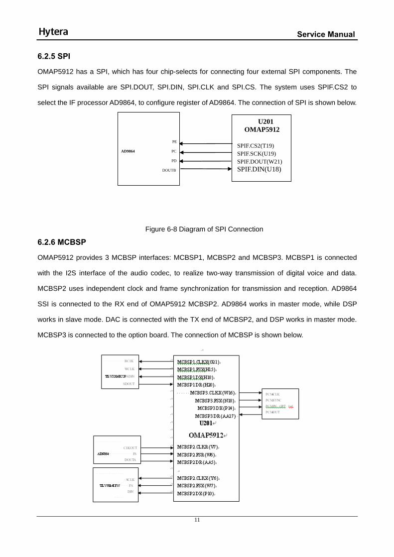
6.2.6 MCBSP
OMAP5912 provides 3 MCBSP interfaces: MCBSP1, MCBSP2 and MCBSP3. MCBSP1 is connected
with the I2S interface of the audio codec, to realize two-way transmission of digital voice and data.
MCBSP2 uses independent clock and frame synchronization for transmission and reception. AD9864
SSI is connected to the RX end of OMAP5912 MCBSP2. AD9864 works in master mode, while DSP
works in slave mode. DAC is connected with the TX end of MCBSP2, and DSP works in master mode.
MCBSP3 is connected to the option board. The connection of MCBSP is shown below.

Service Manual
12
Figure 6-9 Diagram of MCBSP Connection
6.2.7 USB
OMAP5912 provides 3 USB interfaces. One interface integrates a USB transceiver, which is connected
to the accessory jack and is used for program downloading and data application.
Figure 6-10 Diagram of USB Interface
6.2.8 UART
OMAP5912 has three UART interfaces (UART1, UART2 and UART3), and supports hardware flow
control. The maximum communication rate is 1.5Mbps. The connection of UART is shown below. UART1
is connected with the accessory jack, and is used for updating and programming. UART2 is for GPS,
and UART3 is for the option board.
Figure 6-11 Diagram of UART Interface Connection

Service Manual
13
6.2.9 I2C
OMAP5912 provides one I2C interface, and supports communication rate up to 400Kbps. The I2C
interface is connected with the acceleration sensor, and works in slave mode. The connection of I2C is
shown below.
Figure 6-12 Diagram of I2C Connection
6.2.10 MICROWIRE
OMAP5912 provides a MICROWIRE. The four chip select signals can drive four external components.
MICROWIRE is used to configure the audio codec and read the value of its register. It uses the chip
select signal 3. The connection is shown below.
Figure 6-13 Diagram of MICROWIRE Connection
6.2.11 MCSI1
OMAP5912 has two MCSI interfaces. MCSI1 is used for PLL configuration and data transmission. The
connection of MCSI1 is shown below.
Figure 6-14 Diagram of SPI Connection

Service Manual
14
6.3 Audio Section
6.3.1 Audio Diagram
The audio module is mainly for audio input and output. TLV320AIC29 is used as the audio codec to
convert and process audio signal and digital signal. The audio amplifier TDA8547TS is used to amplify
the analog audio signal. DSP processes digital signal (audio signal encoding/decoding, digital I/Q signal
decoding, digital audio signal processing). AD9864 converts and processes the RF IF signal, and sends
the undemodulated serial digital I/Q signal to the DSP for processing. Then DAC5614 converts the digital
signal output by DSP to analog signal.
Figure 6-15 Diagram of Audio Section
6.3.2 Diagram of Signal Flow
The microphone converts the audio signal into electrical signal, which is then amplified by PGA of the
codec and sent to ADC of the codec for sampling. After digital audio processing, the signal is output to
DSP for processing. Then the signal is sent to DAC (TLV5614), which converts the signal to modulation
signal. After modulated and amplified in the RF module, the signal is sent out from the antenna.
The RF signal received by the RF module is converted to digital signal by ADC (AD9864), and is then

Service Manual
15
sent to DSP for demodulation and processing. Then the digital signal is sent to the digital audio
processor of the codec for digital audio processing, and is then converted into analog audio signal by
DAC of the codec. Finally the signal is amplified by the external audio amplifier (TDA8547TS) to drive
the speaker.
OMAP5912
Audio is processed via DSP.
UWIRE.SCLKUWIRE.CS3UWIRE.SDO
UWIRE.SDI
MCLK
MCBSP1.DR
MCBSP1.FSX
MCBSP1.DX
MCBSP1.CLKX
TLV5604DAC
AD9864
MCBSP2.DX DIN
DOUTAMCBSP2.DR
RF TX
RF RX
Internal/external MIC input
APATDA8547TSGain: 31dB
Internal/external speaker output
RX
TXMIC gain: 22dB TX TX
RX RX
Figure 6-16 Diagram of Audio Signal Flow
6.3.3 Audio Amplifier
Main parameters of TDA8547TS are listed in the table below:
Rated Power (Po) 0.5W R L =16Ω Maximum Power (Pmax) 1.2W R L =16Ω
The operation status of the audio amplifier is controlled via GPIO of OMAP. See the table below.
Mode-Amp SEL-SPK MODE SELECT OUT
1 1 0 0 OUT2
1 0 0 1 OUT1
0 1 1 1 Standby

Service Manual
16
6.4 Troubleshooting Flow Chart
The GPS module outputs normally?[1]
Check the power supply.
The channel from GPS to OAMP is normal?
GPS PIN17 outputs 2.8V voltage?
Replace abnormal RC and check OMAP.
Replace the GPS module.
Replace U501.
Replace Z501.
No
Yes
Yes
No
Yes Yes
No
No
Yes
No
NoL506 outputs 2.8V
voltage?
U501 is normal?[3]
Z501 is normal?[4]
Replace the GPS module.
The power supply for GPS is normal?[2]
Yes
No
Description of Normal Situations: [1] The radio shows normal power-on screen, and the backlight is normal. [2] The RF power supply outputs normally, and the RX channel is on. [3] Vpp: 700mV~800mV, F: 19.2MHz.

Service Manual
17
6.5 PCB Difference
For UHF1 PCB, Version H and Version K are made on the basis of Version F.
1. The following changes are made for Version H:
1) Remove the board border and the small board.
2) C802 is compatible with 1206 and 0805.
2. The following changes are made for Version K:
1) Add test points (P609 and P610) for the GPS power supply.
2) Add capacitors C301, C302, C303, C304 and C305.
3) Add R208.
4) Remove the board border.
5) C802 is compatible with 1206 and 0805.
For VHF PCB, Version B is made on the basis of Version A. However, some changes are made for
Version B:
1) Add test points (P609 and P610) for the GPS power supply.
2) Add R208.
3) C802 is compatible with 1206 and 0805.

Service Manual
18
7. GPS Circuit
7.1 Circuit Description
Figure 7-1 Diagram of GPS Circuit
The GPS function is realized via REB-1315LPx. The GPS circuit integrates a baseband processor, a
LNA and a SAW. The 1575.42MHz GPS signal is received by the antenna, and then goes to HPF to
remove the in-band signals used for transmission and reception. After that, the signal goes to BPF to
further remove in-band signals, as well as harmonic and spurious signals. Then the weak GPS signal
goes to a low-noise amplifier (LNA) for amplification. After amplified, the signal goes to the GPS module
for further amplification and filtering, and is then sent to the baseband section for calculation. Then the
calculated GPS positioning information is sent to OMAP via the UART interface. Meanwhile, OMPA can
send appropriate command information to the GPS module via the UART interface. Finally, OMAP sends
the processed data information to LCD.

Service Manual
19
7.2 Schematic Diagram
Figure 7-2 Schematic Diagram

Service Manual
20
7.3 Parts List
No. Ref. No. Part No. Description1 C518 3101051590000 1.5P
2 C519 3199050758000 0.75P
3 C520 3101050100030 1P
4 C527 3101050200010 2P
5 C514 3101051210000 120P
6 C516 3101051590070 1.5P
7 C517 3101051800010 18P
8 C522 3101051040060 0.1U
9 C521 3101051210000 120P
10 C512 3101054710010 470P
11 C515 3101051050000 1UF
12 C513 3101055600000 56P
13 C523 3101051040060 0.1UF
14 C524 3101055600000 56P
15 C525 3101051040060 0.1UF
16 C526 3101051050000 1UF
17 L503 3297106339000 3.3nH
18 L504 3297106339000 3.3nH
19 L501 3297106339000 3.3nH
20 L508 3210305829000 8.2nH
21 L507 3210305180000 18nH
22 L506 3210106390000 39nH
23 L509 3210305829000 8.2nH
24 L502 322150660108 Bead
25 L505 322150660108 Bead
26 R502 3001053310000 330Ώ
27 R501 3001054710000 470Ώ
28 R504 3001051030050 10KΏ
29 R503 3001051010000 100Ώ
30 Z501 3804157560000 GPS filter
31 U501 3609999000300 GPS low-noise amplifier
32 U502 1615000001720 GPS module

Service Manual
21
7.4 Troubleshooting Flow Chart
The GPS module outputs normally?[1]
Check the power supply.
The channel from GPS to OAMP is normal?
GPS PIN17 outputs 2.8V voltage?
Replace abnormal RC and check OMAP.
Replace the GPS module.
Replace U501.
Replace Z501.
No
Yes
Yes
No
Yes Yes
No
No
Yes
No
NoL506 outputs 2.8V
voltage?
U501 is normal?[3]
Z501 is normal?[4]
Replace the GPS module.
The power supply for GPS is normal?[2]
Yes
No
Description of Normal Situations: [1] Detect with a multimeter. The voltage of TP502 changes within the range 1.2V~2.8V. [2] Voltage at L502 and L505: about 3.3V. [3] Gain for U501 (@1.57542GHz): >15dB. [4] Insertion loss for Z501 (@1.57542GHz): <4dB.

Service Manual
22
8. Tuning Description
For details about radio tuning, please refer to the help file of DMR Tuner Software supplied by the Company.

Service Manual
23
9. Interface Definition J1601: 50-Pin Interface Pin No. Name Function Valid Level 2、5、49 GND Power supply: ground (analog) 1 3
AF-CODEC-TO-50PIN AF-50PIN-TO-CODEC
Analog audio signal output/input
4 6
EXT-MIC+ EXT-MIC-
External MIC interface
8 10 12 14 16
IO5-OPT IO4-OPT IO3-OPT IO2-OPT IO1-OPT
GPIO pin of the option board L/H
7 3V6D Power supply: 3.6V 9 11
USB-D+ USB-D-
USB data cable
13 EMERGENCY Emergency key L 32 43
DGND Power supply: ground (digital)
18 GPIO GPIO 20 LED-K-KEY LED indication for key operation L 15 17 19 21
KB-R1 KB-R2 KB-R3 KB-R4
Keyboard row L
22 24 26 28 30
KB-C4 KB-C3 KB-C2 KB-C1 KB-C0
Keyboard column
23 EXT-PTT External PTT detection L 25 27 29
SEL1-Accessory SEL2-Accessory SEL3-Accessory
Accessory identifier L
34 36
UART1-RX-OPT/PS UART1-TX-OPT/PS
UART1
38 40 42 44
UART3-TX-OPT UART3-RX-OPT UART3-CTS/IO30-OPT UART3-RTS/IO29-OPT
UART3
31 33 35
MCBSP3-FSX-OPT MCBSP3-DX-OPT MCBSP3-WCLK-OPT
MCBSP3

Service Manual
24
37 MCBSP3-DR-OPT
39 IIC-SCL-Acce/CLK-32K-OUT
IIC-SDA-Acce (for Version K of UHF1/UHF2/UHF3 and Version B of VHF) CLK-32K-OUT (for Version F/H of UHF1)
41 IIC-SDA-Acce/CLK-OPT
IIC-SCL-Acce (for Version K of UHF1/UHF2/UHF3 and Version B of VHF) CLK-32K-OUT (for Version F/H of UHF1)
46 EXT-BAT+ Power supply for accessory or option board
48 50
IN-SPK- IN-SPK+
Internal speaker
45 47
EXT-SPK- EXT-SPK+
External speaker
J311: 30-Pin LCD Interface Pin No. Name Function Valid Level 1 26
Ground (digital)
2-17 M-D0----M-D15 LCD data 18 /CS-LCD LCD chip select L 19 /RST-OUT Reset signal 20 M-A1 Data and command 21 /WE Write signal L 22 /OE Read signal L 23 IMO 16/8-bit LCD data selection 24 3V3D Power supply: 3.3V 25 VFLASH Power supply for IO 27 3V6D Power supply for backlight 28 29 30
Backlight control L
J821: Channel Board Interface
Pin No. Name Function Valid Level 1 Emergency Emergency L 2 CH2 Channel select 3 CH8 Channel select 4 VOL Volume adjust 5 CH4 Channel select 6 CH1 Channel select

Service Manual
25
7 LED1 Red LED enable H 8 LED2 Green LED enable H 9 GND 10 INT-MIC+780 Microphone+ 11 INT-MIC-780 Microphone- 12 NC/GND NC (for Version K of
UHF1/UHF2/UHF3 and Version B of VHF) GND (for Version F/H of UHF1)
13 PWR-SW- Power-on enable input 14 PWR-SW+ Power-on enable output 15 3V3DRF 3.3V power supply 16 NC/GND NC (for Version K of
UHF1/UHF2/UHF3 and Version B of VHF) GND (for Version F/H of UHF1)
J2: 20-Pin Option Board Interface Pin No. Name Function Valid Level 1 3 5 7 9
IO1-OPT IO2-OPT IO3-OPT IO4-OPT IO5-OPT
GPIO L/H
11 13 15 17
UART3-TX-OPT UART3-RX-OPT UART3-CTS/IO30-OPT UART3-CTS/IO30-OPT
UART3
2 IIC-SDA-Acce/CLK-32K-OUT
IIC-SDA-Acce (for Version K of UHF1/UHF2/UHF3 and Version B of VHF) CLK-32K-OUT (for Version F/H of UHF1)
4 IIC-SCL-Acce/CLK-OPT
IIC-SCL-Acce (for Version K of UHF1/UHF2/UHF3 and Version B of VHF) CLK-32K-OUT (for Version F/H of UHF1)
6 8 10 12
MCBSP3-DR-OPT MCBSP3-WCLK-OPT MCBSP3-DX-OPT MCBSP3-FSX-OPT
MCBSP3
14 Ground (analog) 16 AF-50PIN-TO-CODEC Analog audio signal

Service Manual
26
18 AF-CODEC-TO-50PIN Analog audio signal 19 Ground (digital) 20 3V6D Power supply for digital circuit
16-Pin Accessory Interface Pin No. Name Function Valid Level 1 GND Ground (analog & digital) 2 SPK- External speaker- 3 SEL1-Accessory Accessory identifier 1 L 4 SEL2-Accessory Accessory identifier 2 L 5 Emergency Emergency L 6 SPK+ External speaker+ 7 USB+ / RTS USB+ / RTS 8 USB- / CTS USB- / CTS 9 SWB+ Power supply for the interface 10 MIC- External MIC- 11 GPIO GPIO 12 MIC+ External MIC+
13 SEL3-Accessory Accessory identifier 3 or 1-wire communication interface
L
14 TX TX end of serial port communication
15 RX RX end of serial port communication
16 PTT TX control L Definition of Accessory Identifiers
No. OPT_SEL1 OPT_SEL2 OPT_SEL3 Definition 1 0 0 0 Reserved 2 0 0 1 Reserved 3 0 1 0 USB master mode for the radio 4 0 1 1 For connecting earpieces 5 1 0 0 For connecting MODEM 6 1 0 1 For connecting remote speaker microphones
7 1 1 0 Programming cable (serial port)/
USB slave mode for the radio 8 1 1 1 No accessory

Service Manual
27
10. UHF1 (400-470MHz) Information
10.1 Transmitter Circuit
Figure 10-1 Diagram of Transmitter Circuit
The transmitter circuit is mainly composed of:
① RF power amplifier circuit
② Low-pass filter circuit (for suppressing harmonics)
③ Auto power control circuit (APC) (including temperature detection circuit)
The carrier signal generated by TX VCO is modulated and amplified, and then feeds to the transmitter
circuit. In this circuit, the signal passes through a π-type attenuator first, allowing certain isolation
between the RF power amplifier circuit and TX VCO. Then it goes to a pre-driver amplifier (2SC3356) for
pre-amplification, also providing certain isolation. After that, the signal goes to another pre-driver
amplifier (2SC4988) and a driver amplifier (RD01) for further power amplification, to provide appropriate
signal to the final-stage amplifier (RD07) for final power amplification. After processed by multiple
amplifiers, the signal is processed by a microstrip matcher to complete output impedance matching, so
as to reduce output power loss due to impedance mismatch. Then the signal passes through the TX/RX
switch and goes to the low-pass filter.
The low-pass filter is a high-order Chebyshev filter composed of lumped-parameter inductors and
capacitors. Via this filter, the spurious signal within the stop band can be attenuated as much as possible
while the in-band ripple is within the required range.

Service Manual
28
In the auto power control and temperature detection circuit, the drain current from the driver amplifier
and final-stage amplifier is converted to voltage via the sampling resistor and subtraction circuit
(composed of the first operational amplifier). This voltage is compared with the APC control voltage
(output by DAC) at the second operational amplifier. Then the error voltage, which is output by the
second operational amplifier, controls TX power by controlling the bias voltage at the gates of the
amplifiers (including the driver amplifier and the final-stage amplifier). The temperature sensor detects
the surface temperature of the final-stage amplifier, and converts it to DC voltage. Then the DC voltage is
compared with the voltage corresponding to the protection temperature (generally 80% of the extreme
temperature) of the amplifier. If the surface temperature is too high, the bias voltage of the amplifier will
be reduced, so as to reduce output power. The bias voltage will not be increased until the surface
temperature restores to normal level. This process will be repeated while the radio operates.
10.2 Receiver Circuit
Pi Attenuator
1 2
Figure 10-2 Diagram of Receiver Circuit
The receiver circuit mainly comprises the RF band-pass filter, low-noise amplifier, mixer, IF filter, IF
amplifier and IF processor.
10.2.1 Receiver Front-end
The HF signal from the low-pass filter passes through the electrically tunable band-pass filter controlled
via APC/TV1 level, to remove out-of-band interference signal and to send wanted band-pass signal to
the low-noise amplifier (Q9001). The amplified signal goes to a band-pass filter controlled via APC/TV1
level, to remove out-of-band interference signal generated during amplification, and to send wanted HF

Service Manual
29
signal to the mixer.
The wanted signal passes through the RF band-pass filter and low-noise amplifier and goes to the mixer
(D9017). Meanwhile, the first local oscillator (LO) signal generated by VCO passes through the low-pass
filter and also goes to the mixer (D9017). In the mixer, the wanted signal and the first LO signal are
mixed to generate the first IF signal (73.35MHz). Then the signal passes through a π-type attenuator
(2dB) and the LC, to suppress carrier other than the first IF signal, and to increase the isolation between
the mixer and the IF filter. After that, the first IF signal is processed by the crystal filter (Z9001), and is
sent to the two-stage IF amplifier circuit (composed of 2SC3356) for amplification. Then the amplified
signal goes to the IF processor AD9864(U401) for processing.
10.2.2 Receiver Back-end
Figure 10-3 Diagram of IF Processor
The first IF signal (73.35MHz) output by the IF amplifier goes into AD9864 (U401) via Pin 47, where the
signal is converted to the second IF signal (2.25MHz). Then the signal is converted to digital signal via
ADC sampling, and output via the SSI interface. Finally, the digital signal is sent to DSP (OMAP5912) for
demodulation.
AD9864 employs reference frequency of 19.2MHz and shares the crystal with OMAP. The second LO
VCO comprises an oscillator, a varactor and some other components, to provide the 71.1/75.6MHz LO
signal. The 18MHz clock frequency is generated by the LC resonance loop.

Service Manual
30
10.3 Frequency Generation Unit (FGU)
Figure 10-4 Diagram of FGU
The FGU is composed of VCO and PLL. It is the core module of the whole TX-RX system. This circuit
provides accurate carrier frequency during transmission, and stable LO signal during reception. It has a
direct influence on the performance of the system.
10.3.1 Working Principle of PLL
The 19.2MHz frequency generated by the reference crystal oscillator goes to PLL for division, generating
the reference frequency (i.e. step frequency f1). Meanwhile, the frequency generated by VCO generates
another frequency (f2) through the frequency divider in PLL. Then frequencies f1 and f2 are compared in
the phase detector (PD), to generate continuous pulse current. The current goes to the loop filter for RC
integration, and is then converted to CV voltage. Then the CV voltage is sent to the varactor of VCO. It
adjusts the output frequency of VCO directly until the CV voltage becomes constant. Then PLL is locked,
and the stable frequency output by VCO goes to the TX-RX channel after passing through two buffer
amplifiers.
10.3.2 Working Principle of VCO
VCO employs Colpitts oscillator circuit (the RX oscillator circuit is composed of D102, D103, D106, D107
and L112; the TX oscillator circuit is composed of D108, D109, D110, D101 and L117). It obtains different

Service Manual
31
output frequencies by changing the varactor's control voltage (i.e. CV voltage).
There are two types of VCO: TX VCO and RX VCO. Both types control EMD22 to switch operating
status via OMAP. RX VCO is composed of the oscillator loop and Q104, to provide LO signal. TX VCO is
composed of the oscillator loop and Q108, to provide carrier for TX signal.
10.3.3 Two-point Modulation
In TX mode, the two-point modulation technology is employed, to obtain higher modulation accuracy and
lower 4FSK bit error rate. MOD-VCO and MOD-XO send the modulation signal to the modulation end of
VCO and the reference crystal oscillator of PLL respectively to modulate TX VCO and the reference
crystal oscillator.


Pre-Drive2 Drive-stage Final-stage Tx/Rx Switch Low-pass Filter
Tx_VCO
AD9864
FrequencySynthesizer
Rx_VCO
Band-pass Filter1Low-Noise AmpBand-pass Filter2MixerIF FilterIF Processor IF Amp
Ref. Osc19.2MHZ
.
MOD1
MO
D2+
Freq
err
or s
hift
OMAP
4CH DAC
GPS module
BPF
HPF
ANTMicrostrip Matcher
TV1/APC
LPF
RX/TX VCO
amplifier
TO omap
TV1 /APC
From OMAP
TV1/APC
Reference OSC signal
CV Buffer
Pi Attenuator
1 2
BATT+
Stop band filter
Adapt SW
Adapt control
APC module
Low-Noise Amp
OP
Pre-driver1
RX/TX VCO buffer LPF
LPF
Pi Attenuator
1 2
CV SW
CV-read control
CV out
1
2
P i Attenuator
Pi Attenuator


LDO: 5V
LDO:5V
DC to DC 600mA
DC to DC 600mA
15mA/3V3D
RF PA 7.4V/1.6ARQA0002DNS
Vcc1 /2 2.2V-18V 210mA/Po=0.89W/7.4V
AF PA(TDA8547TS)
DVDD 1.65V-1.8V-1.95V Digital coreIOVDD 2V- 3.6V(MCLK=100M) I/O
2V- 3.6V(MCLK=50M)1.1V-2.5V External
VREF 2.3V-2.5V-2.7V Pro=2.5V SAR ADC reference voltage 1.25V Pro=1.25VVBAT 0.5V-6V Battery monitor input
Codec(TLV320AIC29IRGZR)AVDD1 3V-3.3V-3.6V Audio ADC,DAC,Reference,SAR ADCAVDD2 3V-3.3V-3.6V PLL analogBVDD 3V-4.2V Battery power supplyDRVDD 3V-3.3V-3.6V Headphone driver
Vcc (3.0V-5.5V)/1mA(No load max)
DVDD 4.5V-5V-5.5V(5V Supply) 2.7V-3V-3.3V(3 Supply)
DAC(TLV5604) No load,run clk:: Slow1.4mA/Fast 3.5mA(5V) Slow1mA/Fast 3mA(3V)AVDD 4.5V-5V-5.5V(5V Supply) 2.7V-3V-3.3V(3 Supply)Vref
VCCcp_main: Charge pump supply, 2.7V-5V(3 to 5 V);
VCCdigital: Digital supply, 2.7V-3V-3.3V;
VCCxtal : Crystal oscillator ECL/CML, 2.7V-3V-3.3V;VCCecl/cml: ECL/CML, 2.7V-3V-3.3V;
VDD 3.3V/15mA(EMIFS Bus is used 3V3D)
LCM(TFT)VLED (1*WLED 3.2±0.2V/15mA)
Vcc 2.7V-3.1V /33mA(read while write)
MCU(Nor FLASH+PsRAM))
VDD/Q 1.7V-1.8-1.95V /50mA Operation mode
SDRAM
DVDDI/O(1.71V-1.8V-AVDD)
AVDD(2.4V-2.8V-3.6V)
OMAP5912CVDDCVDD1CVDD2CVDD3CVDDRTC
Low power standby (1.05V-1.1V-1.21V)
Active mode(1.525V-1.6V-1.65V)
core logic and low voltage sections of I/Ocore logicMPU subsystem logic and memoryDSP subsystem logic and memoryRTC core logic
CVDDACVDDDLL
1.525V-1.6V-1.65V
1.525V-1.6V-1.65VAPLL provide 48MHz to peripherals(DDR)SDRAM timing
Peripheral I/O buffersMCSI2 and McBSP2 peripheral I/O buffersFlash I/F I/O buffersMMC/SD1 I/F I/O buffersMcBSP3,MCSI1,UART,USB1 I/O buffersCamera I/F and ETM I/O buffersGPIO,MPUIO,Microwire I/O buffersRTC I/ODDR/SDRAM interface I/O buffers
Low voltage range(1.65V-1.8V-1.95V)
High voltage range(2.5V-2.75Vor 3.3V-3.6V)
DVDD2Not use transceiver1.65V-1.8V-1.95V Internal USB transceiver buffersUse transceiver
3V-3.3V-3.6V
VDDF Positive supply for ADC back endVDDA Positive supply for ADC front endVDDI Positive supply for LNA and MixerVDDQ Positive supply for CLK synthesizerVDDP Positive supply for LO synthesizer charge pump
IF(AD98644) Op :17mA Std :0.01mA VDDL Positive supply for LO synthesizerVDDD Positive supply for Internal digital VDDC Positive supply for CLK synthesizerVDDH Positive supply for digital Interface
Analog voltage2.7V-3V-3.6V
Digital voltage2.7V-3V-3.6V
Interface voltage1.8V- -- -3.6V
Charge pump voltage2.7V-5V-5.5V
Vcc 3.3V/10mA LED
VCO
RX/TX
PLL(SKY72310)
3V3DRF
125uA-1000uA/5VFGU
12.5mA
0.5mA/3V3D
5mA/1V8D
3mA/1V8D
40mA/1.8VD
7.4V
Fuse2.5A/32V
Main Battery
Accelerometer(MMA7455L)
RS232(MAX3232ESE)
0.5mA/3V3A
17mA/3V3A
Vbat/2
2V5 /division
3V3ARF
20mA/3V6D
40mA/3V3D
3.5mA/5VRT
1mA/3V3ARF
5mA/5VFGU
21mA/5VFGU
3V3DRF
TX:53mA/RX:29mA
1mA/3V3D
30mA/3V3D
210MA/1V6D
5mA/3V3D
5VFGU
5VRT
3V6D
3V3A
3V3DRF
3V3D
1V6D
1V8D
16mA/3V3ARF
5VA/150mA; RX/TX/DAC
5VA-RTC/150mA; VCO
RESETRESET(MIN:800mS)
LDO1
6mA/3V3D
Vin_3V3 (3.15V-3.45V)
GPS Module (REB-1315 GSC3F/LPX)V_RTC( 2.5V-3.6V)
10uA /3V6RTC
66mA/3V3D
3V3ARF
2V5 /division
LTC1877
LDO 3V3 150mA
LDO 3V3 150mA
LDO 3V3 150mA
LDO 3V3 150mA
RESET IC
LTC1877
LDO 1V8 150mA
DVDD1DVDD3DVDD5DVDD6DVDD7DVDD8DVDD9DVDDRTC
DVDD4
230mA/7.4V/Po=0.9W
1.6A/7.4V/5W
3V3D
LDO 3V3 150mA
Back-up

5
5
4
4
3
3
2
2
1
1
D D
C C
B B
A A
BAT+
R5V
R5V
R5V
5VRT
BAT+
DISCHARGE-SW-TX3
APC/TV1 1,11
PS-APC 3
ANT-GPS9
PS-RX 3
TEM-LEV-DET-TC 13
IF8
PS-TX 3
LO1
PD780 UHF Schematic Diagram(TX/RX Circuit)
D9007
MA2S077
D9007
MA2S077
12
C9090
0.01u
C9090
0.01u
R90963.3KR90963.3K
R9029330
R9029330
R9025270
R9025270
C9104
0.1U
C9104
0.1U
R90940
R90940
C90641000pC90641000p
R9054
0.39
R9054
0.39
C90411uC90411u
C9050470PC9050470P
C910115pC910115p R9099
1nHR9099
1nH
C90710.1uC90710.1u
R9037NCR9037NC
R9059100K-F
R9059100K-F
C9021
3.6PC9021
3.6P
C91139pC91139p
+ C905122u/10v
+ C905122u/10v
12
Q9018
PBR941
Q9018
PBR941
2
31
C9040ncC9040nc
C911827p
C911827p
R9086NC
R9086NC
DTC114EEQ9007
DTC114EEQ9007
3
1
2
L9011
1uL9011
1u
C9002100PC9002100P
R902147
R902147
R9018
680R9018
680
C9139NC
C9139NC
R9034NCR9034NC
R90983.3K
R90983.3K
R9067
6.8k
R9067
6.8k
C9016
NCC9016
NC
C9053NCC9053NC
C90851000PC90851000P
C9035
22PC9035
22P
C9008nc
C9008nc
C90591000pC90591000p
R9011100
R9011100
D9015
HVC350B
D9015
HVC350B
21
R9046470K-F
R9046470K-F
R90953.3KR90953.3K
L901022nL901022n
C907915pC907915p
C90910.1u
C90910.1u
C9128
4p
C9128
4p
L9039
0
L9039
0
L902539NH
L902539NH
L9015BLM15PD121SN1
L9015BLM15PD121SN1
12
R90414.7KR90414.7K
R9048150K-FR9048150K-F
R90895.6kR90895.6k
R9026ncR9026nc
L900922nHL900922nH
C9004
2pC9004
2p
R90044.4nHR90044.4nH
C9012nc
C9012nc
D9014
HVC350B
D9014
HVC350B
21
C9130ncC9130nc
C9048470PC9048470P
C9037470PC9037470P
C9039470PC9039470P
C910620pC910620p
R9056nc
R9056nc
L90344p
L90344p
C9140nc
C9140nc
R9008
1.5KR9008
1.5K
C90490.1uC90490.1u
R9015330
R9015330
L9026
100n
L9026
100n
L9029NCL9029NC
R9003270R9003270
C9031
9pC9031
9p
L900282n
L900282n
C9007
7PC9007
7P
L9020BLM15PD121SN1L9020
BLM15PD121SN1
12
C91002.7pC91002.7p
GND GND
INOUT
Z900173.35M
GND GND
INOUT
Z900173.35M
1
23
4
56
DTC114EEQ9008
DTC114EEQ9008
3
1
2
C90430.1uC90430.1u
C914147pFC914147pF
C9045470PC9045470P
R9028270R9028270
C9069470PC9069470P
R908047PR908047P
C90951uFC90951uF
Q90062SA1745
Q90062SA1745
1
2 3
C91378pC91378p
R9090ncR9090nc
C902510PC902510P
R9057150K-FR9057150K-F
R90973.3K
R90973.3K
C91334p
C91334p
C90631000pC9063
1000p
R9091ncR9091nc
D9017HSMS-2827
D9017HSMS-2827
1
32
4
C9119NCC9119NC
R905047KR905047K
C90268p
C90268p
C91163.6pC91163.6p
C9029470PC9029470P
C9097
0.1u
C9097
0.1u
C9017
NCC9017
NC
C91112.4p
C91112.4p
L901318nHL901318nH
C90287p
C90287p
C91248pC91248p
C91176p
C91176p
TP9005
TP
TP9005
TP
R9072100KR9072100K
C911218pC911218p
C90149pC90149p
C91077pC91077p
Q9019
EMD22
Q9019
EMD22
1
2
4 3
6
5
R90581M-F
R90581M-F
L903
65T
L903
65T
U9003
LM45
U9003
LM45
+VS1VO 2
GND3
R90233.9KR90233.9K
R9073100KR9073100K
R90278.2kR90278.2k
L90335T
L90335T
C90660.01uC90660.01u
L9022270nHL9022270nH
L9016
3.3nL9016
3.3n
Q90042SC4988Q90042SC4988
1
23
C9081470PC9081470P
C9030
2.4pC9030
2.4p
D9002
1SS356
D9002
1SS356
1 2
C910515pC910515p
C90860.1uC90860.1u
C90891000PC90891000P
D9010EDZ3.6BD9010
EDZ3.6B
12
C90870.047u
C90870.047u
T9002
XFMR
T9002
XFMR
612
43
R90381kR90381k
D9013
HSM88AS
D9013
HSM88AS
321
R9077100KR9077100K
C9009
4PC9009
4P
C90460.1uC90460.1u
L900318nH
L900318nH
C9073nc
C9073nc
C9121
1000P
C9121
1000P
C9070
NC
C9070
NC
R907933KR907933K
C9075470p
C9075470p
ANT1ANT1
1
R9014ncR9014nc
C9018470PC9018470P
C9013470PC9013470P
C90881000pC90881000p
R908456KR908456K
L900418nH
L900418nH
L9038
0
L9038
0
C9034
470P
C9034
470P
C9099
10p
C9099
10p
C91298P
C91298P
TP9004TPTP9004TP
R9093ncR9093nc
R90451M-FR90451M-F
R900933
R900933
C9058NC
C9058NC
C9074nc
C9074nc
L900610nL900610n
U9002
AD8566ARMZ
U9002
AD8566ARMZ
A OUTPUT1A -INPUT2A +INPUT3
V+ 8
B +INPUT 5B -INPUT 6B OUTPUT 7
GND4
C9123ncC9123nc
L9014BLM18SG121TN1L9014BLM18SG121TN1
12
L900518nHL900518nH
C90920.1uFC90920.1uF
C90570.1uC90570.1u
C9126NCC9126NC
TP9003TPTP9003TP
C9011100P
C9011100P
R90331k
R90331k
L9012220nL9012220n
L90355T
L90355T
R90661.5kR90661.5k
C91346P
C91346P
R9002
47KR9002
47K
R906310KR906310K
C902712PC902712P
C9022
NCC9022
NC
C91380.047u
C91380.047u
C9033470P
C9033470P
C9096470pFC9096470pF
C9094NCC9094NC
D9008MA2S077D9008MA2S077
12
L9027820nH
L9027820nH
R904733KR904733K
C91320C91320
C90440.01uC90440.01u
C90380.1uC90380.1u
TP9001APC-outTP9001APC-out
1
C912227pC912227p
D9001
HVC350B
D9001
HVC350B
21
C907710p
C907710p
R903610k
R903610k
Q9017
PBR941
Q9017
PBR9412
31
C9135
4pF
C9135
4pF
R9017
100R9017
100
C902043p
C902043p
R900782
R900782
D9006MA2S077
D9006MA2S077
12
C91317p
C91317p
C90671000pC90671000p
C9047470PC9047470P
C9098
470pF
C9098
470pF
C9110
0.01u
C9110
0.01u
C9042470PC9042470P
R9016
150R9016
150
Q9001AT-41511
Q9001AT-41511 1
243
R9101150K-FR9101150K-F
C9019
9PC9019
9P
R9069
nc
R9069
nc
C9015
8PC9015
8P
Q9020
EMD22
Q9020
EMD22
1
2
43
6
5
C90651500pC90651500p
R9024
6.8KR9024
6.8K
L9031
ncL9031
nc
R9032
NCR9032
NC
L90303.3nHL90303.3nH
C9023
7pC9023
7p
C90611000PC90611000P
C9062NCC9062NC
L900182n
L900182n
R907410kR907410k
R9039
100R9039
100
T9001XFMRT9001XFMR
61 2
43
TP9002LO
TP9002LO
R9085100KR9085100K
R90133.3K
R90133.3K
C9136
4pF
C9136
4pF
C90011000PC90011000P
C9006
NCC9006
NC
D9012
HVC350B
D9012
HVC350B
21
C90031p
C90031p
L900847nHL900847nH
R900610k
R900610k
Q90022SC3356Q90022SC3356
2
31
R907551R907551
C91145.6K
C91145.6K
R9083330R9083330
C91158P
C91158P
C9032
8pC9032
8p
R9068
3.3K
R9068
3.3K
R9012100R9012100
R90433.3K
R90433.3K
L901815n(high Q) L901815n(high Q)
Q9005RD01MUS2
Q9005RD01MUS2
1
32
L901722n(high Q)L901722n(high Q)
R9100150K-FR9100150K-F
L900710nL900710n C9024
8pC9024
8p
L9024220N
L9024220N
R9071330R9071330
C9060
1000PC9060
1000P
L903
75T
L903
75T
R9092ncR9092nc
D9016
nc
D9016
nc
21
D9005MA2S077
D9005MA2S077
12
R908110KR908110K
Q9003RD07MUS2B
Q9003RD07MUS2B
1
32
C912012PC912012P
R902222R902222
C907820pC907820p
R90530.39
R90530.39
L9032
470n
L9032
470n
C90800.1uC90800.1u
C910915p
C910915p
C90931000PC90931000P
R90785.6KR90785.6K
L9028
22n
L9028
22n
C9005NCC9005NC
C9103
1000P
C9103
1000P
R9076100KR9076100K
R90550.39R90550.39

5 4 3 2 1
D
C
B
A A
AD
C_I
N
ADC_IN
PD-CODEC
MICBIAS--HEDA
F-C
OD
EC
-IN
AF-CODEC-OUT
AF-
CO
DE
C-O
UT
AF-CODEC-IN
MICBIAS--HND
1V8D
3V3D
3V3A
3V3A
3V3A
IIS-W
CLK
-CO
DE
C5
IIS-B
LCK
-CO
DE
C5
IIS-D
I-CO
DE
C5
DA
V-C
OD
EC
3
VOL7
CV-ADC1
AF-OUT 12
TEM-LEV-DET-TC14EXT-MIC- 7
EXT-MIC+ 7uW
-CLK
-CO
DE
C5
uW-C
S3-
CO
DE
C5
uW-S
DO
-CO
DE
C5
uW-S
DI-C
OD
EC
5
CLK
-CO
DE
C2
IIS-D
O-C
OD
EC
5
RESET-CODEC3
SEL1-ADC 3
SEL2-ADC 3
PWR-SW-6,7,10,12
INT-MIC+780 7
INT-MIC-780 7
TONE-CODEC 3
SEL-Acoustic 3
AF CODEC TO 50PIN
AF 50PIN to CODEC
Vref=2.5V
Add R823 del C823
PD780 UHF Schematic Diagram(CODEC Circuit)
R841 10KR841 10K
R820
2K
R820
2K
C8500.1uC8500.1u
C856
270P
C856
270PC8330.1uC8330.1u
C858
1500P
C858
1500P
C848
100P
C848
100P
C8210.22uC8210.22u
R82310KR82310K
C8411500PC8411500P C857
270P
C857
270P
L821BLM15PD121SN1
L821BLM15PD121SN1
C845
270P
C845
270P
C826
0.01u
C826
0.01u
L828BLM18AG601SN1
L828BLM18AG601SN1
C8520.1uC8520.1u
C8430.1uC8430.1u
C839
0.1u
C839
0.1u
C824
0.22u
C824
0.22u
R826 47K-FR826 47K-F
C8401uC8401u
R829 470KR829 470K
R83033K-FR83033K-F
C8282.2u/10VC828
2.2u/10V
C853270P
C853270P
U821U821
IOVDD1PWR_DN2RESET3GPIO24GPIO15AVDD26AVSS27AVDD18NC9NC10NC11NC12
AV
SS
113
VR
EF
14V
BA
T15
AU
X2
16A
UX
117
BU
ZZ_I
N/C
P_I
NN
18C
P_O
UTP
19C
P_I
NP
20M
ICIN
_HN
D21
MIC
BIA
S_H
ND
22M
ICIN
_HE
D23
MIC
BIA
S_H
ED
24
MIC_DET 25OUT32N 26SPK1 27SPK2 28DRVDD 29SPKFC 30VGND/CP_OUTN 31DRVSS1 32OUT8N 33BVDD 34OUT8P 35DRVSS2 36
DA
V37
SS
38M
OS
I39
MIS
O40
SC
LK41
MC
LK42
SD
OU
T43
SD
IN44
WC
LK45
BC
LK46
DV
DD
47D
VS
S48
T-P
AD
49
C8370.01uC8370.01u
C831
1u
C831
1u
C822
0.01u
C822
0.01u
C825
2.2u/10V
C825
2.2u/10V
C846
270P
C846
270P
C830
100p
C830
100p
R825 2KR825 2K
C844ncC844nc
TP821TP821 1
R822 0R822 0
R832
2K
R832
2K
R838 10KR838 10K
C851270PC851270P
R835 0R835 0
TP822MIC+TP822MIC+
1
U820U820
EN
AB
LE4
X010X111X12Z11Z2Z03
GN
D6
NC
5
Vcc
14
Y0 16Y1 15
Y 13
A 9B 8C 7
C8360.1uC8360.1u
C8471uC8471u TP823
GNDTP823GND
1
TP820AF-OUTTP820AF-OUT
1
C8341uC8341u
R834 0R834 0
L827BLM18AG601SN1
L827BLM18AG601SN1
L822BLM15PD121SN1
L822BLM15PD121SN1
C842100PC842100P
C849
270P
C849
270P
C835270PC835270P
C827
0.01u
C827
0.01u
C838270PC838270P
C8321uC8321u
R828 15K-FR828 15K-F
R821
100
R821
100
L820BLM18AG601SN1
L820BLM18AG601SN1
R824 15K-FR824 15K-F
L823BLM18AG601SN1
L823BLM18AG601SN1
R833
2K
R833
2K
C829
270P
C829
270P

5 4 3 2 1
D
C
B
A A
BAT++
EXT-SPK- 7
EXT-SPK+ 7
Mode-AMP3
SEL-Acoustic3
AF-OUT13
IN-SPK- 7
IN-SPK+ 7
PWR-SW-6,7,10,13
PD780 UHF Schematic Diagram(AF Amplifier Circuit)
C810
0.1u
C810
0.1u
C8010.1uC8010.1u
R803330KR803330K
L801L801
C806100pC806100p
R80610R80610
R805
10K
R805
10K
TP801TP801
1
C8090.1uC8090.1u
L805L805
U801
TDA8547TS
U801
TDA8547TS
VC
C1
20
VC
C2
11
IN1-17
IN1+16 OUT1- 18
OUT1+ 3IN2-14
IN2+15
SVRR5
MODE4SELECT6
GN
D1
1G
ND
210
OUT2+ 8
OUT2- 13
NC
2N
C7
NC
9N
C12
NC
19
C805100pC805100p
L803L803
R80110R80110
L802
BLM18PG181SN1
L802
BLM18PG181SN1
L804L804R804
10K
R804
10K
DTC114EEQ802DTC114EEQ802
3
1
2
C807270PC807270P
R802330KR802330K
TP802TP802
1
R807
20K
R807
20K
C811270PC811270P
DTC114EEQ801DTC114EEQ801
3
1
2
C802
22u/10V
C802
22u/10V
C8083900pC8083900p
C818270PC818270P
C804
270P
C804
270P
C815
NC*0.01u
C815
NC*0.01u
C816
1u/16V
C816
1u/16V
C814270PC814270P
C8133900pC8133900p
C803
0.22u
C803
0.22u
C8190.01uC8190.01u
C812
0.1u
C812
0.1u
C8170.1uC8170.1u
5 4 3 2 1
D
C
B
A A
5VRT
3V3DRF
MOD-XO 1
APC/TV1 1,14
MOD-VCO 1
MCBSP2-DX-DAC5
MCBSP2-CLKX-DAC5
MCBSP2-FSX-DAC5
LOAD-DAC5
PD-DAC3
TO VCO
TO VCTCXO
PD780 UHF Schematic Diagram(DAC Circuit)
TP702APC/TV1TP702APC/TV1
1
C704470pC704470p
R707
33kR707
33k
R713100R713100
R705 10K-FR705 10K-F
R712BLM15PD121SN1
R712BLM15PD121SN11 2
R701 1KR701 1K
C708100pC708100p
C703470PC703470P
U701TLV5614IPWU701TLV5614IPW
DV
DD
1P
D2
LDA
C3
DIN
4S
CLK
5C
S6
FS7
DG
ND
8R
EFI
NC
D10
AG
ND
9
RE
FIN
AB
15O
UTA
14O
UTB
13O
UTC
12O
UTD
11
AV
DD
16
C7011u/10vC7011u/10v
C7051000PC7051000P
C7061uC7061u
R704 100R704 100
R709
100k
R709
100k
C7100.1uC7100.1u
C712
1u
C712
1u
C7111u
C7111u
R70268kR70268k
R706 10K-FR706 10K-F
R710100kR710100k
TP701MOD2TP701MOD2
1
L702
BLM15PD121SN1
L702
BLM15PD121SN11 2
C7071uC7071u
C709330pC709330p

5
5
4
4
3
3
2
2
1
1
D D
C C
B B
A A
POWER-SW+
POWER-SW+
3V3D
1V6D
5VRT
3V3D
3V6D
5VFGU
GND_SIGNAL
BAT++
3V6D
1V8D
3V3A
BAT++ EXT-BAT+
GND_EARTH
BAT++ 3V3ARFBAT+
3V3GPS
3V3DRF
3V3DRF
EXT-BAT+
3V3DRF
PS-GPS3
PWR-RESET2
PWR-SW+ 6,7
PWR-SW- 6,7,12,13
EXT-PWR 3
POWER-CTL 3
POWER-KEY-DET 3
PD780 UHF Schematic Diagram(Power Circuit)
C616100pFC616100pF
C663NC
C663NC
R631 15KR631 15K
C675
1uF
C675
1uF
C612
0.01uF
C612
0.01uF
U607TPS3808G33QDBVRQ1
U607TPS3808G33QDBVRQ1
RESET1
MR3 GND2Ct 4
VDD 6SENSE 5
L616L616
U611U611
RUN1
SYNC7
VFB3
PLLPF8
ITH2 GN
D4
VIN
6
SW 5
L610L610
Q601Q601
1
2 3
TP6013.3VTP6013.3V
1
C609
1uF
C609
1uF
C645220P/50V
C645220P/50V
U603RP102N331B
U603RP102N331B
VDD1GND2CE3 NC 4
VOUT 5
R614R614
C607
0.1uF
C607
0.1uF
C619C619
L613L613R624R624
L611
BLM18PG181SN1
L611
BLM18PG181SN1
C654C654
11 2 233
C6620.1uFC6620.1uF
C613NC
C613NC
C674220P/50V
C674220P/50V
C6102.2uFC6102.2uF
NC*DTC114EE
Q602
NC*DTC114EE
Q602
3
1
2
U606RP102N331B
U606RP102N331B
VDD1GND2CE3 NC 4
VOUT 5
C6220.1uF/16V
C6220.1uF/16V
C6040.1uF/16V
C6040.1uF/16V
C6400.22UF 10V
C6400.22UF 10V
C6412.2uFC6412.2uF
D604DAN222
D604DAN222
1
23
R627 47KR627 47K
C653NC*2.2uFC653NC*2.2uF
L604
BLM18PG181SN1
L604
BLM18PG181SN1
R601
100K-F
R601
100K-F
U608RP102N331B
U608RP102N331B
VDD1GND2CE3 NC 4
VOUT 5
C611
0.1uF
C611
0.1uF
L614L614
Q605Q605
1
2 3C656
0.1uF
C656
0.1uF
C668
0.1uF
C668
0.1uF
TP6033.6VTP6033.6V
1
TP6051.6VTP6051.6V
1
C669
1uF
C669
1uF
R613 1KR613 1K
L601
BLM18PG181SN1
L601
BLM18PG181SN1
R632 1KR632 1K
L612
BLM18PG181SN1
L612
BLM18PG181SN1
L603
BLM18PG181SN1
L603
BLM18PG181SN1
R626R626
R608
NC
R608
NC
C661C661
11 2 233
C651NC
C651NC
C6830.01uFC6830.01uF
U601U601
RUN1
SYNC7
VFB3
PLLPF8
ITH2 GN
D4
VIN
6
SW 5
C657C657
11 2 233
R604
0
R604
0
L606
BLM18PG181SN1
L606
BLM18PG181SN1
C6145.6pFC6145.6pF
Q6042SK1824Q6042SK1824
2
31
P607P607
1
R628 47KR628 47K
R602R602
C6242.2uFC6242.2uF
C6080.1uFC6080.1uF
C636C636
11 2 233
C637
47uF
C637
47uF
C634NC
C634NC
C648
1uF
C648
1uF
C6780.22uF 10VC678
0.22uF 10V
D602D602
21
U609RP102N331B
U609RP102N331B
VDD1GND2CE3 NC 4
VOUT 5
C6250.1uFC6250.1uF
C6180.1uF/16VC6180.1uF/16V
C681
270P
C681
270P
C646C646
11 2 233
C6380.01uF/16V
C6380.01uF/16V
R617
470K-F
R617
470K-F
C6870.01uFC6870.01uF
C6861500PC6861500P
C676
0.22uF 10V
C676
0.22uF 10V C6012.2uFC6012.2uF
C682
0.1uF/16V
C682
0.1uF/16V
C627C627
11 2 233
R612 1KR612 1K
C647
0.1uF
C647
0.1uF
C6550.22UF 10V
C6550.22UF 10V
L607L607
C6841500PC6841500P
TP6041.8VTP6041.8V
1
D601D601
12
C685270PC685270P
C6034.7uF/16V
C6034.7uF/16V
P606P606
1
U604
TK11250CM
U604
TK11250CM
ON
/OFF
1G
ND
2N
P(V
RE
F)3
VIN
6G
ND
5V
OU
T4
R6292.7KR6292.7K
L615L615
L602BLM18PG181SN1
L602BLM18PG181SN1
R623
150K-F
R623
150K-F
TP602RESETTP602RESET
1
C6214.7uF/16V
C6214.7uF/16V
C667C667
11 2 233
C6260.1uF/16VC6260.1uF/16V
C643NC
C643NC
C6602.2uFC6602.2uF
U612RP102N331B
U612RP102N331B
VDD1GND2CE3 NC 4
VOUT 5
C680
270P
C680
270P
R620
3.3K
R620
3.3K
C6350.1uFC6350.1uF
R622R622
C672
20pF/50V
C672
20pF/50V
C6771uFC677
1uF
F601
2.5A-32V
F601
2.5A-32V
1 2
Q606Q606
1
2 3
C606
2.2uF
C606
2.2uF
R619R619
C6580.1uF/16V
C6580.1uF/16V
C6702.2uFC6702.2uF
C602100pF/16V
C602100pF/16V
C6492.2uFC6492.2uF
C6300.1uF/16V
C6300.1uF/16V
C665
47uF
C665
47uF
U610RP102N181D
U610RP102N181D
VDD1GND2CE3 NC 4
VOUT 5
L609
BLM18PG181SN1
L609
BLM18PG181SN1
C620100pF/16V
C620100pF/16V
C6710.1uFC6710.1uF
DTC114EEQ607
DTC114EEQ607
3
1
2
J601
D-700/BATB
J601
D-700/BATB
123
C6150.1u/16VC615
0.1u/16V
C6280.22UF 10V
C6280.22UF 10V
R625R625
C6500.1uFC6500.1uF
C617
0.1uF/16V
C617
0.1uF/16V
C639
0.1uF
C639
0.1uF
Q603Q603
1
32
R607 100R607 100
R618130K-FR618130K-F
C688
0.1uF
C688
0.1uF
C6051uF/25VC605
1uF/25V
U605
TK11250CM
U605
TK11250CMON
/OFF
1G
ND
2N
P(V
RE
F)3
VIN
6G
ND
5V
OU
T4
C679
0.1uF/16V
C679
0.1uF/16V
C666
0.01uF/16V
C666
0.01uF/16V
R630 47KR630 47K
C652270pFC652270pF
R611
10K
R611
10K
C6420.1uFC6420.1uF
P608P608
1
C673NC
C673NC
R621100KR621100K
L605BLM18PG181SN1
L605BLM18PG181SN1
C6231uF/25VC6231uF/25V
C644
20pF/50V
C644
20pF/50V

5
5
4
4
3
3
2
2
1
1
D D
C C
B B
A A
5VFGU
3V3DRF
3V3A
CLK-IF/PLL 1
CLK-OMAP/IF 2
IF14
PS-2LOC 3
SPI-DIN-IF 5
SPI-SCK-IF 5SPI-DOUT-IF 5SPI-CS2-IF 5
MCBSP2-FSR-IF 5
MCBSP2-CLKR-IF 5
SYNCB-IF 3
MCBSP2-DR-IF 5
PD780 UHF Schematic Diagram(AD9864 Circuit)
TP413FERCLK
TP413FERCLK
1
C464
0.1u
C464
0.1u
D4021SV305
D4021SV3052
1
C4470.01uC4470.01u
R4078.2KR4078.2K
C4312200pC4312200p
C427
220p
C427
220p
C44339PC44339P
Q4012SC4617
Q4012SC4617
2
31
L403 BLM15PD121SN1L403 BLM15PD121SN11 2
R4094.7KR4094.7K
C4650.1uC4650.1u
C44833pC44833p
C451NCC451NC
C428100PC428100P
C46133pC46133p
C4570.01uC4570.01u
RN401 0*4RN401 0*4
12345
678
C421ncC421nc
R412100kR412100k
C4490.01uC4490.01u
C466
0.1u
C466
0.1u
L405
BLM15PD121SN1
L405
BLM15PD121SN1
1 2
C429100PC429100P
C435
0.1u
C435
0.1u
C469
270P
C469
270P
L4136.8UHL4136.8UH
R411390R411390
C4400.01uC4400.01u
C45818pC45818p
C438100PC438100P
TP403GNDTP403GND
1
C43222pC43222p
C450
0.012u
C450
0.012u
C470
270P
C470
270P
C4527PC4527P
R4031KR4031K
R41010kR41010k
C467
2.2u/10v
C467
2.2u/10v
R408100R408100
L410BLM18AG601SN1
L410BLM18AG601SN1
C453 0.01uC453 0.01u
C4410.1uC4410.1u
C4620.1uC4620.1u
C459470PC459470P
C4340.1uC4340.1u
R414 2.7kR414 2.7k
C471
270P
C471
270P
C4722.2uFC4722.2uF
C4375600PC4375600P
R416820RR416820R
C42518pC42518p
C4220.1uC4220.1u
TP404CV2TP404CV2
1
C42012PC42012P
TP4012FLOTP4012FLO
1
R404
680RR404
680R
C439100PC439100P
R40151R40151
D401
HVC350B
D401
HVC350B21
R4131.8kR4131.8k
C4540.01uC4540.01u
C444470PC444470P
C4260.01uC4260.01u
L411 3.3uL411 3.3u
L402
270n
L402
270n
C423
1u
C423
1u
R415
10K
R415
10K
L412 BLM15PD121SN1L412 BLM15PD121SN11 2
+C4680.68u/10v+
C4680.68u/10v
12
C455
3300PC455
3300P
C436
0.01u
C436
0.01u
U401
AD9864
U401
AD9864
MXOP1MXON2GNDF3IF2N4IF2P5VDDF6GCP7GCN8VDDA9GNDA10VREFP11VREFN12
RR
EF13
VDD
Q14
IOU
TC15
GN
DQ
16VD
DC
17G
ND
C18
CLK
P19
CLK
N20
GN
DS
21G
ND
D22
PC23
PD24
PE 25VDDD 26VDDH 27CLKOUT 28DOUTA 29DOUTB 30FS 31GNDH 32SYNCB 33GNDS 34FREF 35GNDL 36G
ND
P37
IOU
TL38
VDD
P39
VDD
L40
CXV
M41
LON
42LO
P43
CXV
L44
GN
DI
45C
XIF
46IF
IN47
VDD
I48
PRPAD 49
L407BLM15PD121SN1
L407BLM15PD121SN1
1 2
C430
0.1u
C430
0.1u
R40210kR40210k
C4563.6pC4563.6p
C46030pC46030p
Q402
UMC4N
Q402
UMC4N
1
2
34
5
Q4032SC3356
Q4032SC3356
2
31
L40410uL40410u
C4420.01uC4420.01u
L409
470nHL409
470nH
C4450.1uC4450.1u
L4084.7uL4084.7u
C433
0.1u
C433
0.1u
L40110uL40110u
C4630.22uC463
0.22u
TP402IF
TP402IF
1
L406220n(HQ)L406220n(HQ)
C4460.1uC4460.1u

5
5
4
4
3
3
2
2
1
1
D D
C C
B B
A A
MOT+
LED-K-LCD
IMO
LED-K-LCD LED-K-KEY
LED-K-KEY
LED1LED2
PTT-KEY
LED1LED2
MOT-
3V3DRF
3V3D
3V3A
3V6D
3V3D3V6D
EXT-BAT+
VFLASH
3V3D
3V3DRF
CH1 3
CH2 3CH8 3
LED-IND1 3
PTT-IO 3
LED-IND2 3
CH4 3
UART1-RX-OPT/PS5,6
UART1-TX-OPT/PS5,6
EMERGENCY 3
KB-C1 5
MOTOR-CTL 3
IIC-SCL-Acce 5
KB-R0 5
KB-C0 5
IIC-SDA-Acce 5
Acce-INT1 3
PWR-SW+ 6,10PWR-SW- 6,10,12,13
VOL 13
KB-C05KB-C15KB-C25KB-C35KB-C45
/RST-OUT3/CS2-LCD 4M-A1 4
M-D2 4M-D34M-D4 4
M-D14 M-D0 4
/WE4 /OE 4
M-D74 M-D6 4M-D54
M-D134 M-D14 4M-D154
M-D8 4M-D94M-D10 4M-D114
M-D12 4
LED-LCD-BL 3 LED-KEY 3
USB-D- 5,6USB-D+ 5,6
EXT-SPK+ 12
EXT-SPK- 12
MCBSP3-DX-OPT 5
MCBSP3-DR-OPT 5MCBSP3-WCLK-OPT 5
MCBSP3-FSX-OPT 5
UART3-RTS/IO29-OPT5UART3-CTS/IO30-OPT5
UART3-TX-OPT5UART3-RX-OPT5
CLK-32K-OUT 2CLK-OPT 2
IO1-OPT3IO2-OPT3IO3-OPT3
IN-SPK-12
IN-SPK+12
IO5-OPT3IO4-OPT3
INT-MIC-780 13INT-MIC+780 13
EXT-MIC-13
EXT-MIC+13
SEL2-Accessory 3SEL3-Accessory 3
EMERGENCY 3KB-R1 5KB-R2 5KB-R3 5KB-R4 5
SEL1-Accessory 3,13
IO to Accessory(TD TEST)3
AF CODEC TO 50PINAF 50PIN to CODEC
EXT-PTT 3
PD780 UHF Schematic Diagram(INT Interface Circuit)
U317U317
X1 A1X2 A2X3 A3X4 A4X5 A5X6 A6
Y1C1Y2C2Y3C3Y4C4Y5C5Y6C6
GN
D1
B1
GN
D2
B2
GN
D3
B3
C315
270p
C315
270p
D318D3181
543 2
6
D309D3092 1
Q310BSH103Q310BSH103
1
32
U318U318
X1 A1X2 A2X3 A3X4 A4X5 A5X6 A6
Y1C1Y2C2Y3C3Y4C4Y5C5Y6C6
GN
D1
B1
GN
D2
B2
GN
D3
B3
J313
JST SM02B-SRSS-TB(LF)
J313
JST SM02B-SRSS-TB(LF)
12
D310D3102 1
C331
270P
C331
270PC334270pC334270p
C313270pC313
270p
C322
270P
C322
270PL305BLM18AG601SN1
L305BLM18AG601SN1
U313U313
X1 A1X2 A2X3 A3X4 A4X5 A5X6 A6
Y1C1Y2C2Y3C3Y4C4Y5C5Y6C6
GN
D1
B1
GN
D2
B2
GN
D3
B3
P312P312 1
U314U314
X1A1X2A2X3A3X4A4X5A5X6A6
Y1 C1Y2 C2Y3 C3Y4 C4Y5 C5Y6 C6
GN
D1
B1
GN
D2
B2
GN
D3
B3
J1601
AXK6F50347YG
J1601
AXK6F50347YG
1234567891011121314151617181920212223242526272829303132333435363738394041424344454647484950
D302
1N4148WS
D302
1N4148WS
12
U316U316
X1 A1X2 A2X3 A3X4 A4X5 A5X6 A6
Y1C1Y2C2Y3C3Y4C4Y5C5Y6C6
GN
D1
B1
GN
D2
B2
GN
D3
B3
L303BLM18PG181SN1
L303BLM18PG181SN1
C319
270p
C319
270p
R328NCR328NC
R324 33R324 33
R321
3.01
R321
3.01
L304BLM18AG601SN1
L304BLM18AG601SN1
J311
DF23C-30DS-0.5V(51)
J311
DF23C-30DS-0.5V(51)
1 23 45 67 89 10
11 1213 1415 1617 1819 2021 2223 2425 2627 2829 30
P314P314 1
C318
0.1u
C318
0.1u
R323 2.2KR323 2.2K
U312U312
X1A1X2A2X3A3X4A4X5A5X6A6
Y1 C1Y2 C2Y3 C3Y4 C4Y5 C5Y6 C6
GN
D1
B1
GN
D2
B2
GN
D3
B3
C332
270P
C332
270P
C321
270P
C321
270P
R322 2.2KR322 2.2K
D305D305
2 1
R325 33R325 33
U320U320
X1A1X2A2X3A3X4A4X5A5X6A6
Y1 C1Y2 C2Y3 C3Y4 C4Y5 C5Y6 C6
GN
D1
B1
GN
D2
B2
GN
D3
B3
C3100.1uC3100.1u
P313P313 1
D306D306
2 1
U310
NC*MMA7455L
U310
NC*MMA7455L
DVdd_IO1GND2NC3IADDR04GND15AVdd6CS7 INT1/DRDY 8INT2 9NC1 10RFU 11SDO 12SDA/SDI/SDO 13SLC/SPC 14
P311P311 1
D304D304
21
R317 10KR317 10KC323
1u
C323
1u
R3153.3KR3153.3K
C333
270P
C333
270P
C3141uC3141u
Q313BSH103Q313
BSH103
1
32
R326 33R326 33
R316 10KR316 10K
C3121u
C3121u
R3143.3KR3143.3K
DTC114EEQ312
DTC114EEQ312
3
1
2
U315U315
X1 A1X2 A2X3 A3X4 A4X5 A5X6 A6
Y1C1Y2C2Y3C3Y4C4Y5C5Y6C6
GN
D1
B1
GN
D2
B2
GN
D3
B3
J821
AXK5F16547YG
J821
AXK5F16547YG
12345678910111213141516
L302BLM18AG601SN1
L302BLM18AG601SN1
TP301TP301
1
R318 NCR318 NC
D307D30721
U319U319X1A1 X2A2 X3A3 X4A4 X5A5 X6A6
Y1 C1Y2 C2Y3 C3Y4 C4Y5 C5Y6 C6
GN
D1
B1
GN
D2
B2
GN
D3
B3
U321U321
X1A1X2A2X3A3X4A4X5A5X6A6
Y1 C1Y2 C2Y3 C3Y4 C4Y5 C5Y6 C6
GN
D1
B1
GN
D2
B2
GN
D3
B3
C317
270p
C317
270p
C320
270p
C320
270p
P310P310 1
C316
270p
C316
270p
R327 100R327 100
R319 0R319 0
U322U322
X1A1X2A2X3A3X4A4X5A5X6A6
Y1 C1Y2 C2Y3 C3Y4 C4Y5 C5Y6 C6
GN
D1
B1
GN
D2
B2
GN
D3
B3
D303D303
21
D308D30821
R313 470R313 470
C311
0.1u
C311
0.1u

5
5
4
4
3
3
2
2
1
1
D D
C C
B B
A A
3V3D
3V3D
3V3D
3V3D
MCBSP3-DX-OPT7MCBSP3-DR-OPT7
KB-R2 7
IIC-SDA-Acce7
SPI-DIN-IF8
UART3-RTS/IO29-OPT 7
KB-R3 7
uW-SDO-CODEC13
UART3-CTS/IO30-OPT 7
KB-R0 7
SPI-SCK-IF8
uW-SDI-CODEC13
UART3-TX-OPT 7
IIS-BLCK-CODEC13
KB-C1 7
UART3-RX-OPT 7
SPI-DOUT-IF8
MCBSP3-WCLK-OPT7
IIS-WCLK-CODEC13
KB-C2 7
MCBSP3-FSX-OPT7
KB-C3 7
IIS-DI-CODEC13
KB-C4 7
IIS-DO-CODEC13
IIC-SCL-Acce7
KB-R4 7
KB-C0 7
KB-R1 7
EMU1 6
TDO 6
/TRST 6TMS 6TDI 6
RTCK 6TCK 6EMU0 6
UART2-RX-GPS 9UART2-TX-GPS 9
USB-D+ 6,7USB-D- 6,7
MCBSP2-CLKR-IF8MCBSP2-FSR-IF8MCBSP2-DR-IF8
MCBSP2-CLKX-DAC11MCBSP2-FSX-DAC11MCBSP2-DX-DAC11
MCSI-CS-PLL1MCSI-CLK-PLL1
MCSI-DO-PLL1
SPI-CS2-IF8
uW-CLK-CODEC13uW-CS3-CODEC13 UART1-TX-OPT/PS 6,7
UART1-RX-OPT/PS 6,7
LOAD-DAC11
SW-CHARGE-FGU1
SW-CHARGE-FGU-io3
SYNCB-IF8
PD780 UHF Schematic Diagram(OMAP SI Circuit)
R26310KR26310K
RN257
100*4
RN257
100*4
12345
678
R219 10KR219 10K
R25810KR25810K
TP269TP269
1
TP264TP264
1
TP255TP255
1
R25610KR25610K
TP263TP263
1
TP260TP260
1
RN2550*4RN2550*4
12345
678
RN26122K*2RN26122K*2
1 234
RN260
100*4
RN260
100*4
12345
678
R262
15K
R262
15K
RN25610K*4RN25610K*4
1 2 3 45678
RN258
100*4
RN258
100*4
12345
678
R261
15K
R261
15K
C267
12P
C267
12P
RN259
0*4
RN259
0*4
12345
678
OMAP5912ZZG-1U201B
OMAP5912ZZG-1U201B
MCBSP1.CLKX/GPIO54G21 MCBSP1.FSX/GPIO53H15
MCBSP1.DX/GPIO52H18MCBSP1.DR/GPIO51H20
SPIF.DIN/GPIO47/uWIRE.SDIU18 SPIF.DOUT/GPIO46/uWIRE.SDOW21
MCBSP3.DX/GPIO43/MCSI1.CLKP14 MCBSP3.CLKX/GPIO42W16
MCSI1.DOUT/GPIO18W14
MCBSP3.FSX/GPIO12/TIMER.EXTCLKN18
MCSI1.SYNC/GPIO9W8 MCSI1.CLK/GPIO7M15
SPIF.CS2/MPUIO4/uWIRE.CS2/LED2T19SPIF.SCK/MPUIO1U19
MCBSP3.DR/MCSI1.SYNCAA17
I2C.SCLT18I2C.SDA/GPIO48V20
MCBSP2.CLKR/GPIO11V7
MCBSP2.CLKX/GPIO20Y6
MCBSP2.FSR/GPIO12W6
MCBSP2.FSX/GPIO21W7
MCBSP2.DR/GPIO19AA5
MCBSP2.DX/GPIO22P10
KP.R0/MPUIO8 G18KP.R1/MPUIO9 F19
KP.R2/MPUIO10 H14KP.R3/MPUIO13 E20KP.R4/MPUIO15 E19
KB.C0/MPUIO0 F18KB.C1/MPUIO6 D20KB.C2/GPIO61 D19KB.C3/GPIO63 E18KB.C4/GPIO27 C21
uWIRE.SDI/GPIO33J14 uWIRE.SDO/GPIO57H19 uWIRE.SCLK/GPIO39J15
NC
E5
NC
L1
UART1.RX/UART1.IRRX/GPIO37 V14UART1.TX/UART1.IRTX Y14
UART2.RX/GPIO18 R9UART2.TX/GPIO17 V6
UART3.RTS/GPIO29 K14UART3.CTS/GPIO30 K15UART3.RX/GPIO31 K19UART3.TX/GPIO32 K18
USB.DM/I2C.SCL/UART1.TX/Z R8USB.DP/I2C.SDA/UART1.RX P9
USB.PUEN W4
TRST Y18TMS V17TDI Y19TDO AA19RTCK Y17TCK W18EMU0 V16EMU1 W17
LCD
.P0
D18
LCD
.P1
B21
LCD
.P2
C19
LCD
.P3
G14
LCD
.P4
H13
LCD
.P5
A20
LCD
.P6
B19
LCD
.P7
C18
LCD
.AC
B15
LCD
.HS
C20
LCD
.PC
LKC
15LC
D.V
SB
18
uWIRE.CS3/GPIO34/CAM.D6J19
TP258TP258
1
TP266TP266
1
TP267TP267
1
TP265TP265
1
TP262TP262
1
R257 100R257 100
TP259TP259
1
TP261TP261
1
C274
12P
C274
12P
R260 1.5KR260 1.5K

5
5
4
4
3
3
2
2
1
1
D D
C C
B B
A A
M-D13M-D14M-D15
/UB/LB
/RST-OUT
/CS3-FLASH
M-D8
SDRAM.A10
M-A9
SDRAM.D10
SDRAM.D7
M-A10
SDRAM.CKE
SDRAM.A3
SDRAM.D0
/OE
M-D7
SDRAM.BA1
SDRAM.A[0..12]
SDRAM.A11 SDRAM.D11
M-A11
SDRAM.D8
M-A12
SDRAM.A4
SDRAM.BA0
M-A1
/CS3-FLASH
M-D8
SDRAM.D12
SDRAM.D9
SDRAM.LDQMSDRAM.D[0..15]
SDRAM.A5
M-A13
SDRAM.CS#
SDRAM.D10
SDRAM.D13
M-A14
SDRAM.A0
M-D9
RDYSDRAM.UDQM
M-D9
M-A2
SDRAM.A6
/OE
RDY/WP/WE
SDRAM.D11
SDRAM.D14
SDRAM.A1
M-A[1..24]
M-A15
M-D0
M-D10SDRAM.WE#
M-A16
SDRAM.A7
SDRAM.D12
SDRAM.CAS#
SDRAM.A12
SDRAM.D15
SDRAM.A2
SDRAM.CLK
M-A1/WE/OEM-D0M-D1M-D2M-D3M-D4M-D5M-D6M-D7
M-D1
M-D11
SDRAM.D1
/WP
SDRAM.A8
SDRAM.D13
M-A17SDRAM.D2
SDRAM.A3M-A18
SDRAM.D0
SDRAM.CKE
M-D2SDRAM.D14
M-D12
SDRAM.A9
SDRAM.D3
M-A3
SDRAM.A4
SDRAM.D1
SDRAM.RAS#
M-A19
M-A4
SDRAM.D15
SDRAM.CS#
M-A20SDRAM.D4
SDRAM.A10
SDRAM.CAS#
M-D13
SDRAM.D2
SDRAM.A5
SDRAM.WE#
SDRAM.D5
M-A5
SDRAM.A11
SDRAM.RAS#
M-A21
M-D14
SDRAM.A6
SDRAM.LDQM
M-D3
SDRAM.A0
/CS2-LCD
SDRAM.D6
SDRAM.A12
M-A6
/CS2-LCD
SDRAM.D3
M-A22
/LB
SDRAM.A7
M-D15
M-D10
SDRAM.UDQM
M-D4
SDRAM.D7
SDRAM.BA0
SDRAM.D4
SDRAM.CLK
M-A7
SDRAM.A8M-A23
SDRAM.D8
/WE
M-D5
SDRAM.D5
SDRAM.A1
SDRAM.BA1
M-A8
SDRAM.A9M-A24
SDRAM.D9
M-D[0..15]
SDRAM.D6
SDRAM.A2
M-D6
/CS1-PsRAM
M-D11
/UB
M-D15
/CS1-PsRAM
M-D12
M-A1M-A2M-A3M-A4M-A5M-A6M-A7M-A8M-A9M-A10M-A11M-A12M-A13M-A14M-A15M-A16M-A17M-A18M-A19M-A20M-A21M-A22M-A23M-A24
M-D0M-D1M-D2M-D3M-D4M-D5M-D6M-D7M-D8M-D9M-D10M-D11M-D12M-D13M-D14
1V8D
1V8D
1V8D
VFLASHVFLASH1V8D
3V3D
VFLASH
M-D13 7M-D14 7M-D15 7
M-D8 7M-D9 7
/CS2-LCD 7
M-D1 7
M-D4 7M-D3 7M-D2 7
M-D6 7M-D5 7
M-D7 7
M-D0 7
M-A1 7/WE 7/OE 7
M-D10 7M-D11 7M-D12 7
/RST-OUT2
1V8D for 256Mbit NOR Flash
3VD for 128Mbit NOR Flash
PD780 UHF Schematic Diagram(OMAP MEM Circuit)
U244
TV00570002CDGB
U244
TV00570002CDGB
A0G1A1F1A2E1A3D1A4F2A5E2A6D2A7C2A8C6A9E6A10F6A11C7A12D7A13E7A14F7A15D8A16G8A17F3A18E3A19D6A20E5A21E8A22F8A23F5
DQ0 J2DQ1 G3DQ2 K3DQ3 H4DQ4 H5DQ5 K6DQ6 G6DQ7 J7DQ8 K2DQ9 H3
DQ10 J3DQ11 K4DQ12 J6DQ13 H6DQ14 K7DQ15 H7
CEfH1 OEH2
RESETD4WP/ACCC4
VCCfJ4
CE1-psJ1
RY/BYfE4
NC1 A1NC2 B1NC3 C1NC4 L1NC5 M1NC6 B2NC7 L2NC8 B3
UBD3 LBC3
WEC5
CE2psD5
VCCpsJ5
NC9 L3NC10 B4NC11 F4NC12 G4NC13 L4NC14 B5NC16 G5NC17 K5NC18 L5NC19 B6
NC22 G7NC23 L7NC24 A8
VSS1G2VSS2J8
NC25 B8
NC21 B7NC20 L6
NC26 H8NC27 L8
NC28 M8
R250 10KR250 10KR249 10R249 10
RN24210K*4RN24210K*4
1234 5
678
C245
0.022u
C245
0.022u
C247
1u
C247
1u
C251
0.01u
C251
0.01u
C252
1000p
C252
1000p
C242
0.022u
C242
0.022u
OMAP5912ZZG-1
U201A
OMAP5912ZZG-1
U201A
FLASH.A1 J8FLASH.A2 D3FLASH.A3 C1FLASH.A4 E4FLASH.A5 D2FLASH.A6 F4FLASH.A7 E3FLASH.A8 J7FLASH.A9 F3
FLASH.A10 G4FLASH.A11 G3FLASH.A12 G2FLASH.A13 K8FLASH.A14 H4FLASH.A15 H3FLASH.A16 K7FLASH.A17 J2FLASH.A18 J4FLASH.A19 J3FLASH.A20 F2FLASH.A21 L8FLASH.A22 K4FLASH.A23 K3FLASH.A24 L7FLASH.A25 E1
FLASH.D0 N4FLASH.D1 N2FLASH.D2 N7FLASH.D3 P2FLASH.D4 P4FLASH.D5 P7FLASH.D6 R2FLASH.D7 R3FLASH.D8 R4FLASH.D9 T2
FLASH.D10 T3FLASH.D11 P8FLASH.D12 U1FLASH.D13 U3FLASH.D14 T4FLASH.D15 V3
FLASH.CLK/FLASH.CS2UOE N3
FLASH.RDY/GPIO10 V2FLASH.ADV L4
FLASH.CS2/FLASH.BAA/FLASH.CS2L M4
FLASH.BE1/FLASH.CS2UWE/GPIO60 M8FLASH.BE0/FLASH.CS2UOE/GPIO59 L3
FLASH.CS0/GPIO62 M7FLASH.CS1/FLASH.CS1L M3
FLASH.CS3/GPIO3 N8
FLASH.OE U4
FLASH.RP/FLASH.CS2UWE W1
FLASH.WE W2FLASH.WP V4
SDRAM.CSG8
SDRAM.DQSHC14SDRAM.DQSLD4
SDRAM.CASB4
SDRAM.DQMLC8 SDRAM.DQMUD10
SDRAM.RASH7 SDRAM.WEH8
SDRAM.A13H11 SDRAM.A12H9 SDRAM.A11H10 SDRAM.A10B8 SDRAM.A9B12 SDRAM.A8G9 SDRAM.A7G11 SDRAM.A6G12 SDRAM.A5B9 SDRAM.A4G10 SDRAM.A3A1 SDRAM.A2B6 SDRAM.A1B2 SDRAM.A0A2
SDRAM.BA1C3 SDRAM.BA0B3
SDRAM.D15C12 SDRAM.D14D12 SDRAM.D13D13 SDRAM.D12C11 SDRAM.D11C13 SDRAM.D10D11 SDRAM.D9D14 SDRAM.D8C10 SDRAM.D7D8 SDRAM.D6C4 SDRAM.D5C7 SDRAM.D4D5 SDRAM.D3D7 SDRAM.D2C5 SDRAM.D1C6 SDRAM.D0D6
SDRAM.CLKC9
SDRAM.CLKXD9
SDRAM.CKEH12
U242MT48H8M16LFB4-75 IT
U242MT48H8M16LFB4-75 IT
DQ0 A8DQ1 B9DQ2 B8DQ3 C9DQ4 C8DQ5 D9DQ6 D8DQ7 E9DQ8 E1DQ9 D2
DQ10 D1DQ11 C2DQ12 C1DQ13 B2DQ14 B1DQ15 A2
A0H7A1H8A2J8A3J7A4J3A5J2A6H3A7H2A8H1A9G3
A11G2A12G1
A10H9
CKEF3
RASF8
UDQMF1
BA1G8 BA0G7
WEF9
CASF7
LDQME8
CSG9
VS
SA
1A
1V
SS
J1J1
VS
SE
3E
3V
SS
QA
3A
3V
SS
QC
3C
3V
SS
QB
7B
7V
SS
QD
7D
7
VD
DE
7E
7V
DD
A9
A9
VD
DJ9
J9
NC E2
CLKF2
VD
DQ
B3
B3
VD
DQ
D3
D3
VD
DQ
A7
A7
VD
DQ
C7
C7
TP242TP2421
C254
1u
C254
1u
C246
0.22u
C246
0.22u
R251 100kR251 100k
R253 NCR253 NC
R243 0R243 0
C243
270P
C243
270P
R254 0R254 0
R252 10KR252 10K
C250100p
C250100p
C244
1500p
C244
1500p
R246 10KR246 10K

5
5
4
4
3
3
2
2
1
1
D D
C C
B B
A A
EXT-PWR 10
PS-RXVCO1
PD-DAC11
SEL2-Accessory7
SEL-Acoustic 12
SEL3-Accessory7
Mode-AMP 12
LED-LCD-BL7
TONE-CODEC13
LED-IND2 7
POWER-CTL 10
PLL-LD1
SW-CHARGE-FGU-io 5
PS-TXVCO1
PS-GPS 10
MOTOR-CTL 7
LED-KEY 7
PS-RX14
CH1 7
PTT-IO 7
DAV-CODEC13
PS-APC 14
CH2 7
LED-IND1 7
CH8 7
CH4 7
Acce-INT1 7
RESET-CODEC13
SEL1-Accessory7
DISCHARGE-SW-TX 14
PS-2LOC8
IO1-OPT7
IO2-OPT7
IO3-OPT7
IO5-OPT7
IO4-OPT7
SEL1-ADC13
SEL2-ADC13
EXT-PTT 7
POWER-KEY-DET 10
EMERGENCY 7
SW-CVread 1
IO to Accessory(TD TEST) 3
PS-TX14
PD780 UHF Schematic Diagram(OMAP IO Circuit)
C289
1500P
C289
1500P
C276
0.1u
C276
0.1u
R216 100R216 100
C277
1500P
C277
1500P
R217 100R217 100
R222 100R222 100
R242 100R242 100
R215 100R215 100
C275
0.1u
C275
0.1u
R220 100R220 100
U201D
OMAP5912ZZG-1
U201D
OMAP5912ZZG-1
GPIO1/UART3.RTS R19
GPIO13/LCD.BLUE0 N19
MPUIO5/LOW_PWR/UART3.RTS T20
GPIO40/BCLKREQ W15
GPIO23/MCLKREQ R10
GP
IO55
/RTC
_WA
KE
_IN
TW
13
MPUIO11 W10
GPIO25/MCSI2.DOUT W9
GPIO0/USB.VBUSR18
MP
UIO
5/M
PU
IO12
W5
MPUIO3/MMC2.DAT1 V8
GP
IO7/
MC
SI2
.SY
NC
V9
MPUIO10/MPUIO7 V10
GPIO57/MMC.CLK V11
GPIO8/TRST Y8
GPIO26/MCSI2.DIN AA9
GPIO27 Y10
GPIO55/MMC.CMD P11
MPUIO9/MPUIO6 W11
GPIO58 R11
GPIO6/MCSI1.DIN/TIMER.EVENT3P19
GPIO4/SPIF.DIN/TIMER.EVENT4P20
GPIO29/LCD.P8D17
GPIO30/LCD.P9D16
GPIO31/LCD.P10C17
GPIO32/LCD.P11B17
GPIO33/LCD.P12G13
GPIO34/LCD.P13A17
GP
IO35
/LC
D.P
14C
16
GP
IO2/
LCD
.P15
D15
GPIO14/LCD.RED0N21
MPUIO1/uWIRE.SCLK V19GPIO2M14
GPIO39/UART1-IRSHDN AA15
GP
IO38
/UA
RT1
-IRS
EL
R14
GPIO62/MCBSP1.CLKSG20
MPUIO12/CAM.D0 L19
GPIO35/CAM.D7/UWIRE.CS0J18
GPIO38/CAM.HSL15
GPIO37/CAM.RSTZM19
MPUIO14/CAM.VS L18
GPIO50/PWT/TIMER.PWM0M18
GPIO15/TIMER.PWM2M20
GPIO49/PWL/TIMER.PWM1L14
GPIO3/MCBSP3.FSX/LED1P18
GPIO11/HDQN20
GPIO7/UART2.RCV Y5
GPIO16/FLASH.CS1U Y1
GPIO5/FLASH.CS2U P3
GPIO45/SPIF.CS0/UART3.TX/MCBSP3.CLKXN14
GPIO44/uWIRE.CS3P15
GPIO56/MCSI1.DIN V15
MPUIO2/SPIF.CS1/uWIRE.CS1 N15
GPIO28/KB.C5G19
TP240TP240
1
R218 100R218 100
R214 100R214 100
R212 100R212 100
R244 100R244 100
R24110KR24110K

1
A A
1V6D
3V3D
1V8D
1V8D
1V6D
1V6DSP
3V3D
3V3D
1V6D
3V3D
3V3DRF
VFLASH
3V3ARF
VFLASH
1V6D
1V6D
1V6DSP
CLK-CODEC13
PWR-RESET10
CLK-OPT7
/RST-OUT4
CLK-32K-OUT7
CLK-OMAP/IF8
PD780 UHF Schematic Diagram(OMAP CORE Circuit)
C201270PC201270P
R201R201
C2120.22uC2120.22u
TP201SCLK-INTP201
SCLK-IN
1
R204 0R204 0
C210
0.22UF 10V
C210
0.22UF 10V
R213
0
R213
0
C2260.22uC2260.22u
L204
BLM18PG181SN1
L204
BLM18PG181SN1
C2131500pC2131500p
C208C208
C2311500pC2311500p
OMAP5912ZZG-1U201C
OMAP5912ZZG-1U201C
VS
SY
13
MPU_BOOTJ20
VSSP12
VS
SA
13V
SS
A21
VS
SB
1V
SS
B5
VS
SB
7V
SS
B16
VS
SF2
0V
SS
G1
VS
SK
2V
SS
K20
VS
SN
1V
SS
R21
VS
SU
2V
SS
W20
VS
SY
3V
SS
AA
1V
SS
AA
7V
SS
AA
21
CVDD A15CVDD M2CVDD Y9CVDD Y20
CVDD1 AA3CVDD2 A3CVDD2 A9CVDD2 E2
CVDD3 B13CVDD3 B20CVDD3 J21CVDD3 R20
CVDDRTC W12
CVDDDLL A11
CVDDA Y21
DVDD1 A19DVDD1 E21DVDD2 AA2DVDD3 Y7
DVDD4 A5DVDD4 A7DVDD4 B10DVDD4 B14
DVDD5 C2DVDD5 H2DVDD5 R1
DVDD6 AA11DVDD7 Y16DVDD8 L21DVDD9 U21
DVDDRTC V12
LDO.FILTER J1
CONFV18
RTC_ON_NOFFY12
OS
C32
K_O
UT
AA
13
OS
C32
K_I
NV
13
CLK
32K
_IN
P13
OS
C1_
OU
TW
3
OS
C1_
INY
2
MPU_RSTU20
PWRON_RESETR12
MCLK/GPIO24V5
BCLK/GPIO17Y15
CLK32K_OUT/GPIO36/MPUIO0/UART1-TXR13
BFAIL/EXT_FIQ/UART3.CTSW19
RST_OUT/GPIO41AA20
SYS_CLK_IN/UART2.BCLKY4
R210 33R210 33
C214270PC214270P
R206 10R206 10
C2061000PC2061000P
C232270PC232270P
C228270PC228270P
C2361uC2361u
R209 10R209 10
C215
0.01uF
C215
0.01uF
C224
470P
C224
470P
C2300.22uC2300.22u
C207C207
R207 33R207 33
R205 100R205 100
C2291u
C2291u
C20320PC20320P
C209
1500p
C209
1500p
TP268TP268
1 C205C205
C2271500pC2271500p
R211R211
C223
470P
C223
470P
OE/ST
GND
OUT
VDD
X203
DSB321SDA
OE/ST
GND
OUT
VDD
X203
DSB321SDA
1
2
3
4
C2180.22uC2180.22u
C225
470P
C225
470P
R208 33R208 33
C2340.22uC2340.22u
C220270PC220270P
C211C211
X201SSP-T7F 12.5pF 20ppm SEIKO
X201SSP-T7F 12.5pF 20ppm SEIKO
12 3
4
L201L201L203L203
C2021000pC202
1000pC204
20P
C204
20P
C2221u
C2221u
C2351500pC2351500p
L202
BLM18PG181SN1
L202
BLM18PG181SN1
C2210.22uC2210.22u
C2191500pC2191500p
R203 10R203 10
C2160.22uC2160.22u

5
5
4
4
3
3
2
2
1
1
D D
C C
B B
A A
PLL-LD
RF
charge
RF
charge
5VFGU
3V3DRF
5VFGU
3V3ARF
5VFGU
5VFGU
5VFGU
3V3ARF
PS-RXVCO 3
MCSI-CS-PLL 5MCSI-CLK-PLL 5
MCSI-DO-PLL 5
PS-TXVCO 3
APC/TV111,14
SW-CHARGE-FGU5
CLK-IF/PLL 8
LO 14
PLL-LD3
SW-CVread3CV-ADC 13
MOD-XO 11
MOD-VCO 11
PD780 UHF Schematic Diagram(FGU Circuit)
C1790.1uC1790.1u
R144
3.3K
R144
3.3K
D1011SV305
D1011SV305
21
Q108NE68519
Q108NE68519
2
31
C15313p
C15313p
R112180K
R112180K
C158
2.2u
C158
2.2u
L117
16nH
L117
16nH
C1611000pC1611000p
C157
2.2U
C157
2.2U
R1143.3KR1143.3K
VCC
OUT
VCONT
GND
X101
19.2MHZ
VCC
OUT
VCONT
GND
X101
19.2MHZ
1
23
4
U104FSA 66U104FSA 66
Vin 1OUT 2GND 3
Vcc5
ON/OFF4
R111
100
R111
100
R1065.6KR1065.6K
D1101SV305
D1101SV305
21
Q106EMD22Q106
EMD22
1
2
43
6
5
L121
BLM15PD121SN1
L121
BLM15PD121SN1
12
C111
3P
C111
3P
+ C1852.2u/10v
+ C1852.2u/10v
12
R136
56
R136
56
C1246P
C1246P
R1093.3kR1093.3k
C1157PC1157P
R1350
R1350
C1473pC1473p
L10512nH(绕线)L10512nH(绕线)
C123 6pC123 6p
R10310
R10310
R14210kR14210k
TP101LF_control
TP101LF_control
1
C1721000PC1721000P
C1660.1uC1660.1u
C14822p
C14822p
L1188.8nH
L1188.8nH
L122BLM15PD121SN1
L122BLM15PD121SN1
12
L10733nL10733n
R143
3.3K
R143
3.3K
L109
BLM15PD121SN1
L109
BLM15PD121SN1
12
C175
270pC175
270p
C1410.1uC1410.1u
C1592200PC1592200P
C145 5pC145 5p
C128 6pC128 6p
C1371000PC1371000P
C113nc
C113nc
D112MA2S111D112MA2S111
1 2
R131 10R131 10
C13027p
C13027p
C105
0.1u
C105
0.1u
R137NC
R137NC
R13251
R13251
Q1012SC5108Q1012SC5108
1
32
TP108
PLLLD
TP108
PLLLD
1
C1293.6pC1293.6p
C1147PC1147P
D103 1SV305D103 1SV30521
C1431P
C1431P
+C1780.33u
+C1780.33u
12
L10312n
L10312n
C13415p
C13415p
TP102VCOFBTP102VCOFB
1
C1820.1uC1820.1u
C1402.2u/10vC1402.2u/10v
C1602200PC1602200P
C1831000pC1831000p
R121100R121100
C1260.1u
C1260.1u
R124
2.7K-F
R124
2.7K-F
C171NC
C171NC
C173100PC173100P
C1631000p
C1631000p
D109 1SV305D109 1SV30521
C146 5pC146 5p
C1841000PC1841000P
Q1022SC3356Q1022SC3356
2
31
U102
TC75W51FU
U102
TC75W51FU
A OUTPUT 1A -INPUT 2A +INPUT 3
V+8
B +INPUT5 B -INPUT6 B OUTPUT7
GND 4
L112
18nH
L112
18nH
C1650.1uC1650.1u
R115180R115180
C1033p
C1033p
Q105
2SC4617
Q105
2SC4617
2
31
C154
1u
C154
1u
C136
470P
C136
470P
C1169PC1169P
Q107EMD22Q107
EMD221
2
43
6
5
C15147PC15147P
C1690.1uC1690.1u
TP106PLLCSTP106
PLLCS
1
R1282.7K-FR128
2.7K-F
L11112nHL11112nH
R10210KR10210K
L106390nHL106
390nH
Q104NE68519
Q104NE68519
2
31
R108
3.3K
R108
3.3K
R12710K-FR12710K-F
R12010KR12010K
C11910pC11910p
D108 1SV305D108 1SV30521
R1188.2KR1188.2K
R1041KR1041K
R113
470R
R113
470R
TP105PLLDATA
TP105PLLDATA
1
R107330RR107330R
C139
470P
C139
470P
C1255.6pC1255.6p
L123
BLM15PD121SN1
L123
BLM15PD121SN1
1 2
L10412nH(绕线)L10412nH(绕线)
R123 100KR123 100K
C168100PC168100P
R10510kR10510k
C13247PC13247P
R1173.3KR1173.3K
C120470PC120470P
C104470PC104470P
C112
3P
C112
3P
L124 470nL124 470n
C1740.01uC1740.01u
R145
33K-F
R145
33K-F
L116390nHL116390nH
D1111SV279D1111SV279
21
C1443pC1443p
R1402.2kR1402.2k
TP107PLLCLK
TP107PLLCLK
1
C181ncC181nc
D102 1SV305D102 1SV30521
C118
470P
C118
470P
D106
1SV305
D106
1SV305
21
C1221.5P
C1221.5P
C101470PC101470P
R10156RR10156R
R146 33K-FR146 33K-FTP103MOD-VCO
TP103MOD-VCO
1
C1640.1uC1640.1u
C1097pC1097p
C138
0.1u
C138
0.1u
D105
MA2S077
D105
MA2S077
12
C1670.1u
C1670.1u
L120
BLM15PD121SN1
L120
BLM15PD121SN1
12
L119
390nH
L119
390nH
L115390nHL115390nH
R130
10
R130
10
C152
4.5P
C152
4.5P
C1210.1uC1210.1u
L10133nL10133n
C1621000pF
C1621000pF
R13410R13410
R13847R13847
R12910KR12910K
R1164.7KR1164.7K
C142470PC142470P
R122
10k
R122
10kR125
2.7K-F
R125
2.7K-F
C1078p
C1078p
D104
MA2S077
D104
MA2S077
12
R1108.2KR1108.2K
C1087pC1087p
C127470PC127470P
U103sky72310
U103sky72310
VCCecl/cml1Fvco_main2Fvco_main3
LD/PS_main4VCCcp_main5CPout_main6
N/C7Xtalacgnd/OSC8Xtalin/OSC9Xtalout/NC10VCCxtal11GNDXtal12 N/C 13N/C 14N/C 15N/C 16N/C 17
VCCdigital 19
Data 20CS 21Clock 22
N/C 23Mux_out 24
N/C 18
Pow
erP
AD
25
C1023p
C1023p
C170100PC170100P
R119
100
R119
100
C1561000PC1561000P
TP104RFCVTP104RFCV
1
L114390nHL114
390nH
C1109pC1109p
U101FSA 66
U101FSA 66
Vin 1OUT 2GND 3
Vcc5
ON/OFF4
L113390nHL113390nH
R126nc
R126nc
L108390nHL108390nH
R139
1K
R139
1K
C1491.5P
C1491.5P
C1770.33uC1770.33u
C176
330pC176
330p
C1065p
C1065p
C1337P
C1337P
R141
OR
R141
OR
R13310KR13310K
C117
0.1u
C117
0.1u
L10212nL10212n
L110390nHL110390nH
C1801000pC1801000p
D1071SV305
D1071SV305
21
Q103EMD22
Q103EMD22
1
2
43
6
5

5
5
4
4
3
3
2
2
1
1
D D
C C
B B
A A
3V3D
TMS 5TDI 5TDO 5RTCK 5TCK 5EMU0 5EMU1 5
USB-D- 5,7
/TRST 5
USB-D+ 5,7 PTT-IO 3USB
PD780 UHF Schematic Diagram(EXT Interface Circuit)
RN302 100*4RN302 100*412345
678
R3074.7K
R3074.7K
C325270pC325270p
R309 100R309 100
RN301 100*4RN301 100*4
12345
678
S302S30212
C3060.1uC306
0.1u
R301100KR301100K
R304100KR304100K
D301
KPT-1608SURC
D301
KPT-1608SURC
1 2
J304NC*JTAG
J304NC*JTAG
1234567891011121314
C307270pC307270p
R305100KR305100K
R3064.7K
R3064.7K
J302
nc-CON6
J302
nc-CON6
123456
L301BLM15PD121SN1
L301BLM15PD121SN1
R308 4.7KR308 4.7K

5
5
4
4
3
3
2
2
1
1
D D
C C
B B
A A
MIC-MIC+
PWR-SW-
INT-MIC+780
CH1
CH2
LED1
CH4
CH8VOL
LED2
INT-MIC-780
CH4CH4CH2
PWR-SW+PWR-SW-
PWR-SW+
LED2 VOL
VOL-HCH1CH8LED1 PWR-SW-
VOL-H
VOL-H
EMERGENCY
3V3DRF
1V8D-VOL
3V3DRF
3V3DRF
R
G
PD780 UHF Schematic Diagram(SW Board Circuit)
S1002S1002
12
3
45
C1001
270P
C1001
270P
B1001
OBE-27P42
B1001
OBE-27P42
+1-2
R1001 120R1001 120
C1003
270P
C1003
270P
D1005D1005
21
C1012
270P
C1012
270P
C1005
270P
C1005
270P
D1014D1014
21
S1003
EMERGENCY KEY
S1003
EMERGENCY KEY
123
4567
D1008D1008
21
C1010
270P
C1010
270P
D1013D1013
21
C1006
270P
C1006
270P
1C C4 2
8
S1001
1C C4 2
8
S1001
1234
56
D1003D1003
21
U1002RP102N181D
U1002RP102N181D
VDD1GND2CE3 NC 4
VOUT 5
C1016
0.1uF
C1016
0.1uF
D1006D1006
21
Q1001
UMG3N
Q1001
UMG3N
1
2
34
5
D1004D1004
21
U1001
CM1418-02CS
U1001
CM1418-02CS
A1
A2
A3B1
B2B3
C1008
270P
C1008
270P
D1002
12-22RG/TR8
D1002
12-22RG/TR8
12
3
D1009D1009
21R1002 120R1002 120
C10150.1uFC10150.1uF
D1011D1011
21
J1001AXK6F16547YG
J1001AXK6F16547YG
12345678910111213141516
D1007D1007
21
C1002
270P
C1002
270P
C1007
270P
C1007
270P
L1002
BLM18PG181SN1
L1002
BLM18PG181SN1
C1011
270P
C1011
270P
C10170.1uFC10170.1uF
D1001D1001
21
L1001
BLM18PG181SN1
L1001
BLM18PG181SN1
C1004
270P
C1004
270P

5
5
4
4
3
3
2
2
1
1
D D
C C
B B
A A
KB-C4
KB-C3
KB-C2
KB-C1
KB-C0
KB-R4
KB-R3
KB-R2
KB-R1
KEY-LED-K
VBUS
UART1-TX
UART1-RX
KB-C0
USB-D+
OPT-SEL1
KB-R4PTT
EXT-SPK-
KB-C3KB-C2
EXT-SPK+
KB-C1 OPT-SEL2OPT-SEL3
USB-D-
KB-C4KEY-LED-K
KB-R1EMERGENCY
EXT-MIC-EXT-MIC+
KB-R2KB-R3
IN-SPK+IN-SPK-
IN-SPK+
EXT-MIC+
IN-SPK-
UART1-TXUART1-RXEXT-MIC-
EXT-SPK+EXT-SPK-OPT-SEL3OPT-SEL2
USB-D-
OPT-SEL1PTTEMERGENCY
USB-D+
VBUS
3V6D
EXT-BAT+
3V6D
EXT-BAT+
BACK MENU UP
# 9 6 3 Cancel
0
*
8
7
5
4
2
1
DOWN
OK
IO to Vbus-Accessory
PD780 UHF Schematic Diagram(Keyboard Circuit)
S1703S1703
1 2
D1703D17031
5 432
6
S1715S1715
1 2
D1701D1701
1
5 432
6
R1705100R1705100
D1702D1702
1
5 432
6
D1706PESD12VS1UB
D1706PESD12VS1UB
21
R1702100R1702100
S1710S1710
1 2
D1723 PESD5V0S1UBD1723 PESD5V0S1UB
2 1
S1708S1708
1 2
D1717
19-2
13/W
1D-A
NP
HY
/3T
D1717
19-2
13/W
1D-A
NP
HY
/3T
12
R1708100R1708100
S1713S1713
1 2
D1711 PESD5V0S1UBD1711 PESD5V0S1UB21U1701CM1418-02CSU1701CM1418-02CS
A1
A2
A3B1
B2B3
S1718S1718
12
D1722 PESD5V0S1UBD1722 PESD5V0S1UB2 1
R1701 100R1701 100
J1702
MOLEX543630289
J1702
MOLEX543630289
1234567891011121314151617181920
S1702S1702
1 2
D1710 PESD5V0S1UBD1710 PESD5V0S1UB21
D1707PESD12VS1UB
D1707PESD12VS1UB
21
D1712 PESD5V0S1UBD1712 PESD5V0S1UB21
S1701S1701
12
S1707S1707
12
D1718
19-2
13/W
1D-A
NP
HY
/3T
D1718
19-2
13/W
1D-A
NP
HY
/3T
12
D1705PESD12VS1UB
D1705PESD12VS1UB
21
R1707100R1707100
R1704100R1704100
C1701 2.2uFC1701 2.2uF
S1706S1706
12
S1711S1711
12
S1704S1704
1 2
D1708PESD12VS1UB
D1708PESD12VS1UB
21
D1715
19-2
13/W
1D-A
NP
HY
/3T
D1715
19-2
13/W
1D-A
NP
HY
/3T
12
S1716S1716
12
S1709S1709
1 2
S1714S1714
1 2
D1719
19-2
13/W
1D-A
NP
HY
/3T
D1719
19-2
13/W
1D-A
NP
HY
/3T
12D1725 PESD5V0S1UBD1725 PESD5V0S1UB
2 1
J1701AXK5F50547YG 50pin
J1701AXK5F50547YG 50pin
1234567891011121314151617181920212223242526272829303132333435363738394041424344454647484950
R1706100R1706100
D1709PESD12VS1UB
D1709PESD12VS1UB
21
D1724
PESD5V0S1UB
D1724
PESD5V0S1UB
21
S1712S1712
1 2
R1703100R1703100
D1721 PESD5V0S1UBD1721 PESD5V0S1UB
2 1
D1716
19-2
13/W
1D-A
NP
HY
/3T
D1716
19-2
13/W
1D-A
NP
HY
/3T
12
D1714
19-2
13/W
1D-A
NP
HY
/3T
D1714
19-2
13/W
1D-A
NP
HY
/3T
12
S1717S1717
12
D1713 PESD5V0S1UBD1713 PESD5V0S1UB21
S1705S1705
1 2
D1720
19-2
13/W
1D-A
NP
HY
/3T
D1720
19-2
13/W
1D-A
NP
HY
/3T
12

Service Manual
59
10.7 Parts List
Main Board for PD70X/ PD70XG/ PD78X/ PD78XG/ HD705/ HD705G/ HD785/ HD785G
No. Ref. No. Part No. Description
1 C9132 3001050000000 0Ω
2 R135 3001050000000 0Ω
3 R141 3001050000000 0Ω
4 R204 3001050000000 0Ω
5 R213 3001050000000 0Ω
6 R243 3001050000000 0Ω
7 R254 3001050000000 0Ω
8 R319 3001050000000 0Ω
9 R822 3001050000000 0Ω
10 R834 3001050000000 0Ω
11 R835 3001050000000 0Ω
12 R9094 3001050000000 0Ω
13 L9038 3001060000000 0Ω
14 L9039 3001060000000 0Ω
15 R602 3001060000000 0Ω
16 R604 3001060000000 0Ω
17 R9053 3099080398010 0.39Ω
18 R9054 3099080398010 0.39Ω
19 R9055 3099080398010 0.39Ω
20 R9005 3001055690000 5.6Ω
21 R103 3001051000000 10Ω
22 R130 3001051000000 10Ω
23 R131 3001051000000 10Ω
24 R134 3001051000000 10Ω
25 R203 3001051000000 10Ω
26 R206 3001051000000 10Ω
27 R209 3001051000000 10Ω
28 R249 3001051000000 10Ω
29 R801 3001051000000 10Ω
30 R806 3001051000000 10Ω
31 R9022 3001052200000 22Ω
32 R324 3001053300000 33Ω
33 R325 3001053300000 33Ω
34 R326 3001053300000 33Ω
35 R9009 3001053300000 33Ω
36 R207 3001063300000 33Ω
37 R208 3001063300000 33Ω
38 R210 3001063300000 33Ω
39 R138 3001054700000 47Ω
40 R9021 3001054700000 47Ω
41 R132 3001055100020 51Ω

Service Manual
60
No. Ref. No. Part No. Description
42 R401 3001055100020 51Ω
43 R9075 3001055100020 51Ω
44 R101 3001055600000 56Ω
45 R136 3001055600000 56Ω
46 R503 3001051010000 100Ω
47 R111 3001051010000 100Ω
48 R119 3001051010000 100Ω
49 R121 3001051010000 100Ω
50 R205 3001051010000 100Ω
51 R257 3001051010000 100Ω
52 R327 3001051010000 100Ω
53 R408 3001051010000 100Ω
54 R607 3001051010000 100Ω
55 R713 3001051010000 100Ω
56 R821 3001051010000 100Ω
57 R9011 3001051010000 100Ω
58 R9012 3001051010000 100Ω
59 R9017 3001051010000 100Ω
60 R9039 3001051010000 100Ω
61 R212 3001061010000 100Ω
62 R214 3001061010000 100Ω
63 R215 3001061010000 100Ω
64 R216 3001061010000 100Ω
65 R217 3001061010000 100Ω
66 R218 3001061010000 100Ω
67 R220 3001061010000 100Ω
68 R222 3001061010000 100Ω
69 R242 3001061010000 100Ω
70 R244 3001061010000 100Ω
71 R9016 3001051510000 150Ω
72 R115 3001051810010 180Ω
73 R9001 3001052710010 270Ω
74 R9003 3001052710010 270Ω
75 R9025 3001052710010 270Ω
76 R9028 3001052710010 270Ω
77 R502 3001053310010 330Ω
78 R9015 3001053310010 330Ω
79 R9071 3001053310010 330Ω
80 R9083 3001053310010 330Ω
81 R411 3001053910000 390Ω
82 R113 3001054710000 470Ω
83 R313 3001054710000 470Ω
84 R501 3001054710000 470Ω
85 R404 3001056810000 680Ω

Service Manual
61
No. Ref. No. Part No. Description
86 R9018 3001056810000 680Ω
87 R416 3001058210000 820Ω
88 R139 3001051020000 1KΩ
89 R403 3001051020000 1KΩ
90 R613 3001051020000 1KΩ
91 R701 3001051020000 1KΩ
92 R9033 3001051020000 1KΩ
93 R9038 3001051020000 1KΩ
94 R260 3001051520000 1.5KΩ
95 R9008 3001051520000 1.5KΩ
96 R9066 3001051520000 1.5KΩ
97 R413 3001051820000 1.8KΩ
98 R820 3001052020020 2KΩ
99 R825 3001052020020 2KΩ
100 R832 3001052020020 2KΩ
101 R833 3001052020020 2KΩ
102 R140 3001052220000 2.2KΩ
103 R322 3001052220000 2.2KΩ
104 R323 3001052220000 2.2KΩ
105 R414 3001052720000 2.7KΩ
106 R629 3001054720000 4.7KΩ
107 R108 3001053320000 3.3KΩ
108 R109 3001053320000 3.3KΩ
109 R114 3001053320000 3.3KΩ
110 R117 3001053320000 3.3KΩ
111 R143 3001053320000 3.3KΩ
112 R144 3001053320000 3.3KΩ
113 R314 3001053320000 3.3KΩ
114 R315 3001053320000 3.3KΩ
115 R620 3001053320000 3.3KΩ
116 R9013 3001053320000 3.3KΩ
117 R9043 3001053320000 3.3KΩ
118 R9068 3001053320000 3.3KΩ
119 R9095 3001053320000 3.3KΩ
120 R9096 3001053320000 3.3KΩ
121 R9097 3001053320000 3.3KΩ
122 R9098 3001053320000 3.3KΩ
123 R116 3001054720000 4.7KΩ
124 R409 3001054720000 4.7KΩ
125 R9041 3001054720000 4.7KΩ
126 C9114 3001055620000 5.6KΩ
127 R106 3001055620000 5.6KΩ
128 R9078 3001055620000 5.6KΩ
129 R9089 3001055620000 5.6KΩ

Service Manual
62
No. Ref. No. Part No. Description
130 R9024 3001056820000 6.8KΩ
131 R9067 3001056820000 6.8KΩ
132 R110 3001058220000 8.2KΩ
133 R118 3001058220000 8.2KΩ
134 R407 3001058220000 8.2KΩ
135 R9027 3001058220000 8.2KΩ
136 R102 3001051030000 10KΩ
137 R105 3001051030000 10KΩ
138 R122 3001051030000 10KΩ
139 R129 3001051030000 10KΩ
140 R133 3001051030000 10KΩ
141 R142 3001051030000 10KΩ
142 R241 3001051030000 10KΩ
143 R246 3001051030000 10KΩ
144 R250 3001051030000 10KΩ
145 R252 3001051030000 10KΩ
146 R256 3001051030000 10KΩ
147 R258 3001051030000 10KΩ
148 R263 3001051030000 10KΩ
149 R316 3001051030000 10KΩ
150 R317 3001051030000 10KΩ
151 R402 3001051030000 10KΩ
152 R611 3001051030000 10KΩ
153 R804 3001051030000 10KΩ
154 R805 3001051030000 10KΩ
155 R838 3001051030000 10KΩ
156 R841 3001051030000 10KΩ
157 R9006 3001051030000 10KΩ
158 R9036 3001051030000 10KΩ
159 R9063 3001051030000 10KΩ
160 R9074 3001051030000 10KΩ
161 R9081 3001051030000 10KΩ
162 R219 3001061030010 10KΩ
163 R410 3001061030010 10KΩ
164 R415 3001061030010 10KΩ
165 RN242 3005051030010 10KΩ
166 RN243 3005051030010 10KΩ
167 RN256 3005051030010 10KΩ
168 R261 3001051530000 15KΩ
169 R262 3001051530000 15KΩ
170 R631 3001051530000 15KΩ
171 R824 3001051530010 15KΩ
172 R828 3001051530010 15KΩ
173 R807 3001052030000 20KΩ

Service Manual
63
No. Ref. No. Part No. Description
174 R145 3001053330000 33KΩ
175 R146 3001053330000 33KΩ
176 R707 3001053330000 33KΩ
177 R830 3001053330000 33KΩ
178 R9047 3001053330000 33KΩ
179 R9079 3001053330000 33KΩ
180 R627 3001054730010 47KΩ
181 R628 3001054730010 47KΩ
182 R630 3001054730010 47KΩ
183 R826 3001054730010 47KΩ
184 R9084 3001055630000 56KΩ
185 R702 3001056830000 68KΩ
186 R601 3001051040000 100KΩ
187 R123 3001051040000 100KΩ
188 R251 3001051040000 100KΩ
189 R412 3001051040000 100KΩ
190 R621 3001051040000 100KΩ
191 R709 3001051040000 100KΩ
192 R710 3001051040000 100KΩ
193 R9072 3001051040000 100KΩ
194 R9073 3001051040000 100KΩ
195 R9076 3001051040000 100KΩ
196 R9077 3001051040000 100KΩ
197 R9085 3001051040000 100KΩ
198 R618 3001051340000 130KΩ
199 R623 3001051540000 150KΩ
200 R9048 3001051540000 150KΩ
201 R9057 3001051540000 150KΩ
202 R112 3001051840000 180KΩ
203 R617 3001054740010 470KΩ
204 R829 3001054740010 470KΩ
205 R9046 3001054740010 470KΩ
206 R9059 3001051040000 100KΩ
207 C519 3199050758000 0.75PF
208 C520 3101050100030 1PF
209 C143 3101060100010 1PF
210 C9003 3101060100010 1PF
211 C527 3101050200010 2PF
212 C9004 3101060200010 2PF
213 C102 3101050300000 3PF
214 C103 3101050300000 3PF
215 C111 3101050300000 3PF
216 C112 3101050300000 3PF
217 C144 3101060300010 3PF

Service Manual
64
No. Ref. No. Part No. Description
218 C147 3101060300010 3PF
219 C129 3101063690000 3.6PF
220 C456 3101063690000 3.6PF
221 C9021 3101063690000 3.6PF
222 C106 3101050500010 5PF
223 C145 3101060500010 5PF
224 C146 3101060500010 5PF
225 C125 3101065690000 5.6PF
226 C124 3101050600010 6PF
227 C9117 3101050600010 6PF
228 C9134 3101050600010 6PF
229 C123 3101060600010 6PF
230 C128 3101060600010 6PF
231 C108 3101050700010 7PF
232 C109 3101050700010 7PF
233 C114 3101050700010 7PF
234 C115 3101050700010 7PF
235 C9028 3101050700010 7PF
236 C9107 3101050700010 7PF
237 C9131 3101050700010 7PF
238 C133 3101060700020 7PF
239 C452 3101060700020 7PF
240 C9007 3101060700020 7PF
241 C9023 3101060700020 7PF
242 C9026 3101050800000 8PF
243 C107 3101050800000 8PF
244 C9032 3101050800000 8PF
245 C9115 3101050800000 8PF
246 C9124 3101050800000 8PF
247 C9129 3101050800000 8PF
248 C9137 3101050800000 8PF
249 C9015 3101060800010 8PF
250 C9024 3101060800010 8PF
251 C110 3101050900000 9PF
252 C116 3101050900000 9PF
253 C9014 3101050900000 9PF
254 C9113 3101050900000 9PF
255 C119 3101051000020 10PF
256 C9025 3101051000020 10PF
257 C9077 3101051000020 10PF
258 C9099 3101051000020 10PF
259 C267 3101051200020 12PF
260 C274 3101051200020 12PF
261 C420 3101051200020 12PF

Service Manual
65
No. Ref. No. Part No. Description
262 C9120 3101051200020 12PF
263 C9027 3101061200000 12PF
264 C153 3101061300000 13PF
265 C9079 3101051500020 15PF
266 C9101 3101051500020 15PF
267 C9105 3101051500020 15PF
268 C9109 3101051500020 15PF
269 C134 3101061500010 15PF
270 C425 3101051800010 18PF
271 C517 3101051800010 18PF
272 C458 3101061800000 18PF
273 C9112 3101061800000 18PF
274 C672 3101052000020 20PF
275 C203 3101052000020 20PF
276 C204 3101052000020 20PF
277 C644 3101052000020 20PF
278 C9078 3101052000020 20PF
279 C9106 3101052000020 20PF
280 C432 3101052200010 22PF
281 C9035 3101052200010 22PF
282 C148 3101062200010 22PF
283 C9118 3101052700000 27PF
284 C9122 3101052700000 27PF
285 C130 3101062700010 27PF
286 C460 3101063000010 30PF
287 C448 3101053300000 33PF
288 C132 3101054700010 47PF
289 C151 3101054700010 47PF
290 C223 3101054710010 470PF
291 C224 3101054710010 470PF
292 C225 3101054710010 470PF
293 C512 3101054700010 47PF
294 C9141 3101054700010 47PF
295 R9080 3101054700010 47PF
296 C513 3101055600000 56PF
297 C524 3101055600000 56PF
298 C168 3101051010030 100PF
299 C170 3101051010030 100PF
300 C173 3101051010030 100PF
301 C280 3101051010030 100PF
302 C281 3101051010030 100PF
303 C284 3101051010030 100PF
304 C288 3101051010030 100PF
305 C428 3101051010030 100PF

Service Manual
66
No. Ref. No. Part No. Description
306 C429 3101051010030 100PF
307 C438 3101051010030 100PF
308 C439 3101051010030 100PF
309 C602 3101051010030 100PF
310 C616 3101051010030 100PF
311 C620 3101051010030 100PF
312 C708 3101051010030 100PF
313 C805 3101051010030 100PF
314 C806 3101051010030 100PF
315 C830 3101051010030 100PF
316 C842 3101051010030 100PF
317 C848 3101051010030 100PF
318 C9002 3101051010030 100PF
319 C9011 3101061010010 100PF
320 C427 3101052210010 220PF
321 C645 3101052210010 220PF
322 C674 3101052210010 220PF
323 C201 3101052700000 27PF
324 C469 3101052710000 270PF
325 C845 3101052710000 270PF
326 C175 3101052710000 270PF
327 C207 3101052710000 270PF
328 C214 3101052710000 270PF
329 C220 3101052710000 270PF
330 C228 3101052710000 270PF
331 C232 3101052710000 270PF
332 C243 3101052710000 270PF
333 C282 3101052710000 270PF
334 C283 3101052710000 270PF
335 C286 3101052710000 270PF
336 C287 3101052710000 270PF
337 C313 3101052710000 270PF
338 C315 3101052710000 270PF
339 C316 3101052710000 270PF
340 C317 3101052710000 270PF
341 C319 3101052710000 270PF
342 C320 3101052710000 270PF
343 C321 3101052710000 270PF
344 C322 3101052710000 270PF
345 C331 3101052710000 270PF
346 C332 3101052710000 270PF
347 C333 3101052710000 270PF
348 C334 3101052710000 270PF
349 C470 3101052710000 270PF

Service Manual
67
No. Ref. No. Part No. Description
350 C471 3101052710000 270PF
351 C652 3101052710000 270PF
352 C680 3101052710000 270PF
353 C681 3101052710000 270PF
354 C685 3101052710000 270PF
355 C709 3101052710000 270PF
356 C804 3101052710000 270PF
357 C807 3101052710000 270PF
358 C811 3101052710000 270PF
359 C814 3101052710000 270PF
360 C818 3101052710000 270PF
361 C829 3101052710000 270PF
362 C835 3101052710000 270PF
363 C838 3101052710000 270PF
364 C846 3101052710000 270PF
365 C849 3101052710000 270PF
366 C851 3101052710000 270PF
367 C853 3101052710000 270PF
368 C856 3101052710000 270PF
369 C857 3101052710000 270PF
370 C101 3101054710010 470PF
371 C104 3101054710010 470PF
372 C118 3101054710010 470PF
373 C120 3101054710010 470PF
374 C127 3101054710010 470PF
375 C136 3101054710010 470PF
376 C139 3101054710010 470PF
377 C142 3101054710010 470PF
378 C444 3101054710010 470PF
379 C459 3101054710010 470PF
380 C703 3101054710010 470PF
381 C704 3101054710010 470PF
382 C9018 3101054710010 470PF
383 C9029 3101054710010 470PF
384 C9033 3101054710010 470PF
385 C9034 3101054710010 470PF
386 C9037 3101054710010 470PF
387 C9039 3101054710010 470PF
388 C9042 3101054710010 470PF
389 C9045 3101054710010 470PF
390 C9047 3101054710010 470PF
391 C9048 3101054710010 470PF
392 C9050 3101054710010 470PF
393 C9069 3101054710010 470PF

Service Manual
68
No. Ref. No. Part No. Description
394 C9075 3101054710010 470PF
395 C9081 3101054710010 470PF
396 C9096 3101054710010 470PF
397 C9098 3101054710010 470PF
398 C9013 3101064710000 470PF
399 C137 3101051020010 1000PF
400 C156 3101051020010 1000PF
401 C161 3101051020010 1000PF
402 C162 3101051020010 1000PF
403 C163 3101051020010 1000PF
404 C172 3101051020010 1000PF
405 C180 3101051020010 1000PF
406 C183 3101051020010 1000PF
407 C184 3101051020010 1000PF
408 C202 3101051020010 1000PF
409 C206 3101051020010 1000PF
410 C252 3101051020010 1000PF
411 C705 3101051020010 1000PF
412 C9001 3101051020010 1000PF
413 C9059 3101051020010 1000PF
414 C9061 3101051020010 1000PF
415 C9064 3101051020010 1000PF
416 C9067 3101051020010 1000PF
417 C9085 3101051020010 1000PF
418 C9088 3101051020010 1000PF
419 C9089 3101051020010 1000PF
420 C9093 3101051020010 1000PF
421 C9103 3101051020010 1000PF
422 C9121 3101051020010 1000PF
423 C9060 3101061020000 1000PF
424 C289 3101051520000 1500PF
425 C209 3101051520000 1500PF
426 C213 3101051520000 1500PF
427 C219 3101051520000 1500PF
428 C227 3101051520000 1500PF
429 C231 3101051520000 1500PF
430 C235 3101051520000 1500PF
431 C244 3101051520000 1500PF
432 C275 3101051520000 1500PF
433 C276 3101051520000 1500PF
434 C277 3101051520000 1500PF
435 C684 3101051520000 1500PF
436 C686 3101051520000 1500PF
437 C841 3101051520000 1500PF

Service Manual
69
No. Ref. No. Part No. Description
438 C858 3101051520000 1500PF
439 C9065 3101051520000 1500PF
440 C159 3101052220010 2200PF
441 C160 3101052220010 2200PF
442 C431 3101052220010 2200PF
443 C455 3101063320000 3300PF
444 C215 3101051030020 0.01UF
445 C174 3101051030020 0.01UF
446 C251 3101051030020 0.01UF
447 C426 3101051030020 0.01UF
448 C436 3101051030020 0.01UF
449 C440 3101051030020 0.01UF
450 C447 3101051030020 0.01UF
451 C449 3101051030020 0.01UF
452 C453 3101051030020 0.01UF
453 C454 3101051030020 0.01UF
454 C457 3101051030020 0.01UF
455 C612 3101051030020 0.01UF
456 C638 3101051030020 0.01UF
457 C666 3101051030020 0.01UF
458 C683 3101051030020 0.01UF
459 C687 3101051030020 0.01UF
460 C819 3101051030020 0.01UF
461 C822 3101051030020 0.01UF
462 C826 3101051030020 0.01UF
463 C827 3101051030020 0.01UF
464 C837 3101051030020 0.01UF
465 C9044 3101051030020 0.01UF
466 C9066 3101051030020 0.01UF
467 C9090 3101051030020 0.01UF
468 C9110 3101051030020 0.01UF
469 C619 3101061030010 0.01UF
470 C442 3101061030010 0.01UF
471 C450 3101061230000 0.012UF
472 C242 3101052230000 0.022UF
473 C245 3101052230000 0.022UF
474 C617 3101051040060 0.1UF
475 C630 3101051040060 0.1UF
476 C658 3101051040060 0.1UF
477 C105 3101051040060 0.1UF
478 C117 3101051040060 0.1UF
479 C121 3101051040060 0.1UF
480 C126 3101051040060 0.1UF
481 C138 3101051040060 0.1UF

Service Manual
70
No. Ref. No. Part No. Description
482 C141 3101051040060 0.1UF
483 C164 3101051040060 0.1UF
484 C165 3101051040060 0.1UF
485 C166 3101051040060 0.1UF
486 C167 3101051040060 0.1UF
487 C169 3101051040060 0.1UF
488 C179 3101051040060 0.1UF
489 C182 3101051040060 0.1UF
490 C310 3101051040060 0.1UF
491 C311 3101051040060 0.1UF
492 C318 3101051040060 0.1UF
493 C422 3101051040060 0.1UF
494 C430 3101051040060 0.1UF
495 C433 3101051040060 0.1UF
496 C434 3101051040060 0.1UF
497 C435 3101051040060 0.1UF
498 C441 3101051040060 0.1UF
499 C445 3101051040060 0.1UF
500 C446 3101051040060 0.1UF
501 C462 3101051040060 0.1UF
502 C464 3101051040060 0.1UF
503 C465 3101051040060 0.1UF
504 C466 3101051040060 0.1UF
505 C522 3101051040060 0.1UF
506 C523 3101051040060 0.1UF
507 C525 3101051040060 0.1UF
508 C604 3101051040060 0.1UF
509 C607 3101051040060 0.1UF
510 C608 3101051040060 0.1UF
511 C611 3101051040060 0.1UF
512 C615 3101051040060 0.1UF
513 C618 3101051040060 0.1UF
514 C622 3101051040060 0.1UF
515 C625 3101051040060 0.1UF
516 C626 3101051040060 0.1UF
517 C635 3101051040060 0.1UF
518 C639 3101051040060 0.1UF
519 C642 3101051040060 0.1UF
520 C647 3101051040060 0.1UF
521 C650 3101051040060 0.1UF
522 C656 3101051040060 0.1UF
523 C662 3101051040060 0.1UF
524 C668 3101051040060 0.1UF
525 C671 3101051040060 0.1UF

Service Manual
71
No. Ref. No. Part No. Description
526 C679 3101051040060 0.1UF
527 C682 3101051040060 0.1UF
528 C688 3101051040060 0.1UF
529 C710 3101051040060 0.1UF
530 C801 3101051040060 0.1UF
531 C809 3101051040060 0.1UF
532 C810 3101051040060 0.1UF
533 C812 3101051040060 0.1UF
534 C817 3101051040060 0.1UF
535 C833 3101051040060 0.1UF
536 C836 3101051040060 0.1UF
537 C839 3101051040060 0.1UF
538 C843 3101051040060 0.1UF
539 C850 3101051040060 0.1UF
540 C852 3101051040060 0.1UF
541 C9038 3101051040060 0.1UF
542 C9043 3101051040060 0.1UF
543 C9046 3101051040060 0.1UF
544 C9049 3101051040060 0.1UF
545 C9057 3101051040060 0.1UF
546 C9071 3101051040060 0.1UF
547 C9080 3101051040060 0.1UF
548 C9086 3101051040060 0.1UF
549 C9091 3101051040060 0.1UF
550 C9092 3101051040060 0.1UF
551 C9097 3101051040060 0.1UF
552 C9104 3101051040060 0.1UF
553 C234 3101052240010 0.22UF
554 C212 3101052240010 0.22UF
555 C216 3101052240010 0.22UF
556 C218 3101052240010 0.22UF
557 C221 3101052240010 0.22UF
558 C226 3101052240010 0.22UF
559 C230 3101052240010 0.22UF
560 C246 3101052240010 0.22UF
561 C821 3101052240010 0.22UF
562 C824 3101052240010 0.22UF
563 C210 3101062240000 0.22UF
564 C628 3101062240000 0.22UF
565 C640 3101062240000 0.22UF
566 C655 3101062240000 0.22UF
567 C676 3101062240000 0.22UF
568 C678 3101062240000 0.22UF
569 C463 3101072240000 0.22UF

Service Manual
72
No. Ref. No. Part No. Description
570 C468 3104076840020 0.68UF
571 C9041 3101051050000 1UF
572 C646 3110061050000 1uF
573 C657 3110061050000 1uF
574 C667 3110061050000 1uF
575 C154 3101051050000 1UF
576 C222 3101051050000 1UF
577 C229 3101051050000 1UF
578 C236 3101051050000 1UF
579 C247 3101051050000 1UF
580 C254 3101051050000 1UF
581 C312 3101051050000 1UF
582 C314 3101051050000 1UF
583 C323 3101051050000 1UF
584 C423 3101051050000 1UF
585 C515 3101051050000 1UF
586 C526 3101051050000 1UF
587 C706 3101051050000 1UF
588 C707 3101051050000 1UF
589 C711 3101051050000 1UF
590 C712 3101051050000 1UF
591 C831 3101051050000 1UF
592 C832 3101051050000 1UF
593 C834 3101051050000 1UF
594 C840 3101051050000 1UF
595 C847 3101051050000 1UF
596 C9095 3101051050000 1UF
597 C605 3101061050020 1UF
598 C609 3101061050020 1UF
599 C623 3101061050020 1UF
600 C648 3101061050020 1UF
601 C669 3101061050020 1UF
602 C675 3101061050020 1UF
603 C677 3101061050020 1UF
604 C701 3101061050020 1UF
605 C472 3101062250000 2.2UF
606 C140 3101062250000 2.2UF
607 C157 3101062250000 2.2UF
608 C158 3101062250000 2.2UF
609 C467 3101062250000 2.2UF
610 C601 3101062250000 2.2UF
611 C606 3101062250000 2.2UF
612 C610 3101062250000 2.2UF
613 C624 3101062250000 2.2UF
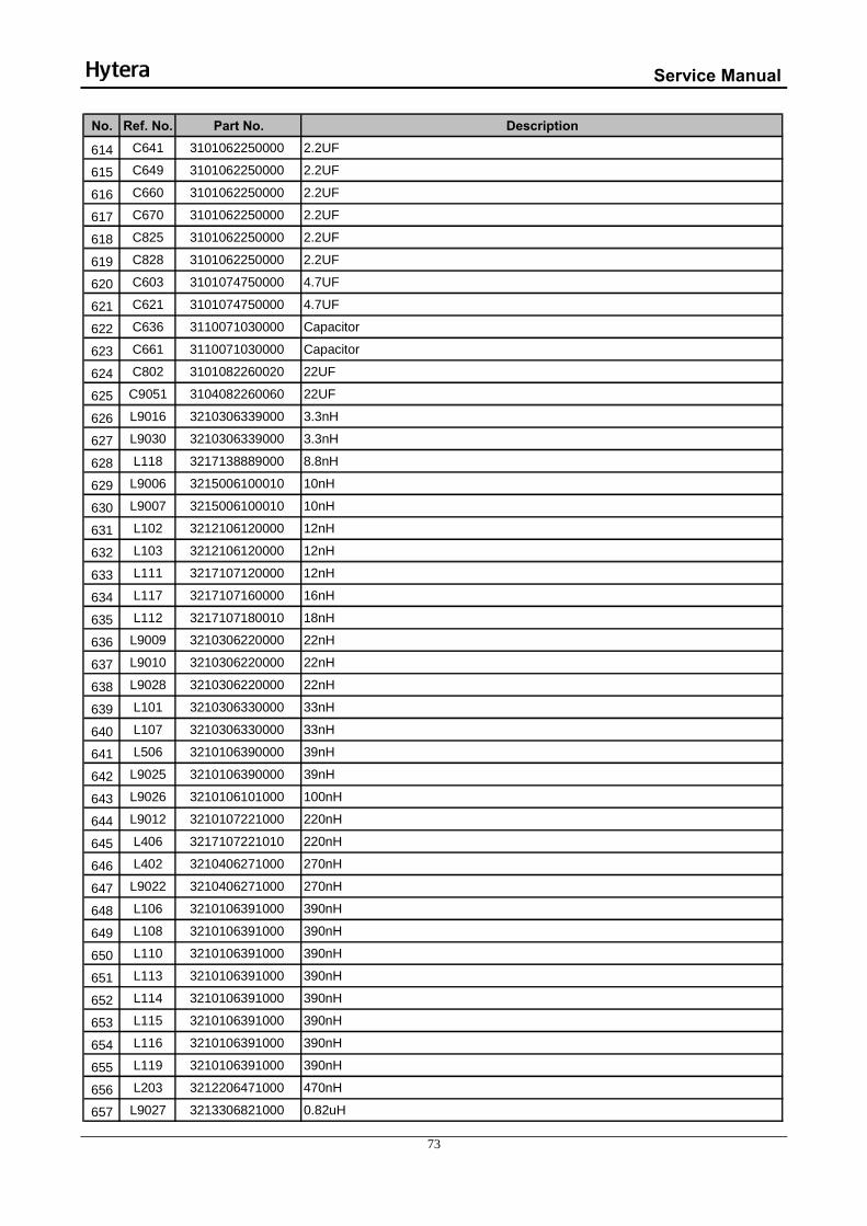
Service Manual
73
No. Ref. No. Part No. Description
614 C641 3101062250000 2.2UF
615 C649 3101062250000 2.2UF
616 C660 3101062250000 2.2UF
617 C670 3101062250000 2.2UF
618 C825 3101062250000 2.2UF
619 C828 3101062250000 2.2UF
620 C603 3101074750000 4.7UF
621 C621 3101074750000 4.7UF
622 C636 3110071030000 Capacitor
623 C661 3110071030000 Capacitor
624 C802 3101082260020 22UF
625 C9051 3104082260060 22UF
626 L9016 3210306339000 3.3nH
627 L9030 3210306339000 3.3nH
628 L118 3217138889000 8.8nH
629 L9006 3215006100010 10nH
630 L9007 3215006100010 10nH
631 L102 3212106120000 12nH
632 L103 3212106120000 12nH
633 L111 3217107120000 12nH
634 L117 3217107160000 16nH
635 L112 3217107180010 18nH
636 L9009 3210306220000 22nH
637 L9010 3210306220000 22nH
638 L9028 3210306220000 22nH
639 L101 3210306330000 33nH
640 L107 3210306330000 33nH
641 L506 3210106390000 39nH
642 L9025 3210106390000 39nH
643 L9026 3210106101000 100nH
644 L9012 3210107221000 220nH
645 L406 3217107221010 220nH
646 L402 3210406271000 270nH
647 L9022 3210406271000 270nH
648 L106 3210106391000 390nH
649 L108 3210106391000 390nH
650 L110 3210106391000 390nH
651 L113 3210106391000 390nH
652 L114 3210106391000 390nH
653 L115 3210106391000 390nH
654 L116 3210106391000 390nH
655 L119 3210106391000 390nH
656 L203 3212206471000 470nH
657 L9027 3213306821000 0.82uH

Service Manual
74
No. Ref. No. Part No. Description
658 L9011 3210209102010 1uH
659 L607 3290299220000 Inductor
660 L613 3290299220000 Inductor
661 L615 3290299220000 Inductor
662 L616 3290299220000 Inductor
663 L411 3213212332000 3.3uH
664 L408 3210407472000 4.7uH
665 L413 3213306682000 6.8uH
666 L614 3217099153000 15uH
667 L610 3217099153000 15uH
668 L502 3221506601080 Bead
669 L505 3221506601080 Bead
670 L302 3221506601000 Bead
671 L304 3221506601000 Bead
672 L305 3221506601000 Bead
673 L410 3221506601000 Bead
674 L820 3221506601000 Bead
675 L823 3221506601000 Bead
676 L827 3221506601000 Bead
677 L828 3221506601000 Bead
678 L9014 3221506121000 Bead
679 L109 3221505121010 Bead
680 L120 3221505121010 Bead
681 L121 3221505121010 Bead
682 L122 3221505121010 Bead
683 L123 3221505121010 Bead
684 L403 3221505121010 Bead
685 L405 3221505121010 Bead
686 L407 3221505121010 Bead
687 L412 3221505121010 Bead
688 L702 3221505121010 Bead
689 L801 3221505121010 Bead
690 L803 3221505121010 Bead
691 L804 3221505121010 Bead
692 L805 3221505121010 Bead
693 L821 3221505121010 Bead
694 L822 3221505121010 Bead
695 L9015 3221505121010 Bead
696 L9020 3221505121010 Bead
697 R712 3221505121010 Bead
698 R614 3221506181000 Bead
699 L202 3221506181000 Bead
700 L204 3221506181000 Bead
701 L303 3221506181000 Bead

Service Manual
75
No. Ref. No. Part No. Description
702 L601 3221506181000 Bead
703 L602 3221506181000 Bead
704 L603 3221506181000 Bead
705 L604 3221506181000 Bead
706 L605 3221506181000 Bead
707 L606 3221506181000 Bead
708 L609 3221506181000 Bead
709 L611 3221506181000 Bead
710 L612 3221506181000 Bead
711 L802 3221506181000 Bead
712 R622 3221506181000 Bead
713 F601 4099000000050 Fuse
714 L9003 3233099185900 18.5nH
715 L9004 3233099185900 18.5nH
716 L9005 3233099185900 18.5nH
717 L9013 3233099185900 18.5nH
718 L9008 3233099470000 47nH
719 T9001 5406000000200 Transformer
720 T9002 5406000000200 Transformer
721 D104 3303020100080 Switching diode
722 D105 3303020100080 Switching diode
723 D9005 3303020100080 Switching diode
724 D9006 3303020100080 Switching diode
725 D9007 3303020100080 Switching diode
726 D9008 3303020100080 Switching diode
727 D101 3304010100220 Varactor
728 D102 3304010100220 Varactor
729 D103 3304010100220 Varactor
730 D106 3304010100220 Varactor
731 D107 3304010100220 Varactor
732 D108 3304010100220 Varactor
733 D109 3304010100220 Varactor
734 D110 3304010100220 Varactor
735 D402 3304010100220 Varactor
736 D401 3304060300050 Varactor
737 D9001 3304060300050 Varactor
738 D9012 3304060300050 Varactor
739 D9014 3304060300050 Varactor
740 D9015 3304060300050 Varactor
741 D112 3303020100020 Switching diode
742 D9002 3303030800040 Switching diode
743 D302 3303990000010 Switching diode
744 D601 3399990000110 Diode
745 D9010 3399990000080 Zener diode

Service Manual
76
No. Ref. No. Part No. Description
746 D9013 3399990000260 Rectifier diode
747 D9017 3301250300000 Schottky barrier diode
748 D307 3399040600020 ESD protection diode
749 D308 3399040600020 ESD protection diode
750 D309 3399040600020 ESD protection diode
751 D310 3399040600020 ESD protection diode
752 D602 3399040600020 ESD protection diode
753 Q101 3401002000990 NPN transistor
754 Q9002 3408002000000 NPN transistor
755 Q102 3408002000000 NPN transistor
756 Q403 3408002000000 NPN transistor
757 Q9017 3404006000000 NPN transistor
758 Q9018 3404006000000 NPN transistor
759 Q103 3403999000000 Transistor
760 Q106 3403999000000 Transistor
761 Q107 3403999000000 Transistor
762 Q9019 3403999000000 Transistor
763 Q9020 3403999000000 Transistor
764 Q104 3408002000080 NPN transistor
765 Q108 3408002000080 NPN transistor
766 Q105 3403003000060 NPN transistor
767 Q401 3403003000060 NPN transistor
768 Q402 3499000000150 Transistor
769 Q9001 3418001000010 NPN transistor
770 Q9004 3406001000090 NPN transistor
771 Q605 3410001000020 PNP Transistor
772 Q9006 3410001000020 PNP Transistor
773 Q312 3403008000010 Transistor
774 Q607 3403008000010 Transistor
775 Q801 3403008000010 Transistor
776 Q802 3403008000010 Transistor
777 Q9007 3403008000010 Transistor
778 Q9008 3403008000010 Transistor
779 Q606 3401001000490 PNP Transistor
780 Q604 3503020000030 N-MOSFET
781 U102 3605002057290 Operational amplifier
782 U103 3604019000000 PLL
783 U401 3603999000000 IF processor
784 U701 3606010000010 D/A converter
785 U9003 5404000000060 Sensor
786 X101 3701019250030 TCXO 19.2MHZ
787 Z9001 3802733540020 Crystal filter
788 X201 3701327610060 Crystal 32.768KHz
789 U201 3610010000010 MCU OMAP5912ZZG

Service Manual
77
No. Ref. No. Part No. Description
790 U604 3608020005750 Power management IC
791 U605 3608020005750 Power management IC
792 U610 3608006000030 Power management IC
793 U603 3608006000000 Power management IC
794 U606 3608006000000 Power management IC
795 U608 3608006000000 Power management IC
796 U609 3608006000000 Power management IC
797 U612 3608006000000 Power management IC
798 U801 3602023005740 Audio amplifier
799 U312 3805000000030 EMI filter
800 U313 3805000000030 EMI filter
801 U314 3805000000030 EMI filter
802 U315 3805000000030 EMI filter
803 U316 3805000000030 EMI filter
804 U317 3805000000030 EMI filter
805 U318 3805000000030 EMI filter
806 U319 3805000000030 EMI filter
807 U320 3805000000030 EMI filter
808 U321 3805000000030 EMI filter
809 U322 3805000000030 EMI filter
810 U601 3608011000050 Power management IC
811 U611 3608011000050 Power management IC
812 U820 3616037000020 Switch
813 U607 3609010000170 Reset IC
814 U821 3613010000000 Baseband processor
815 U244 3612002000020 NOR-FLASH+PSRAM
816 J313 5202002100200 Board-to-wire connector
817 J311 5201030000040 Board-to-board connector
818 J601 5205003100020 Battery connector
819 C627 3110081040000 Capacitor
820 C654 3110081040000 Capacitor
821 RN257 3005061010000 100Ω
822 RN258 3005061010000 100Ω
823 RN260 3005061010000 100Ω
824 ANT1 6201847000000 Antenna spring plate
825 C514 3101051210000 120PF
826 C521 3101051210000 120PF
827 U242 3612044000010 Mobile-SDRAM
828 C178 3101073340010 0.33UF
829 C9019 3101060900010 9PF
830 C9031 3101060900010 9PF
831 C122 3101061590010 1.5PF
832 C149 3101061590010 1.5PF
833 C177 3101073340000 0.33UF

Service Manual
78
No. Ref. No. Part No. Description
834 L9002 3210306820000 82nH
835 R104 3001051020010 1KΩ
836 R632 3001051020010 1KΩ
837 C9128 3101050400010 4PF
838 C9133 3101050400010 4PF
839 C9135 3101050400010 4PF
840 C9136 3101050400010 4PF
841 C518 3101051590000 1.5PF
842 C9100 3101052790000 2.7PF
843 C176 3101053310030 330PF
844 C208 3101053310030 330PF
845 C9116 3101053690000 3.6PF
846 C9087 3101054730000 0.047UF
847 C9138 3101054730000 0.047UF
848 C461 3101063300000 33PF
849 C9020 3101064300000 43PF
850 C637 3110994760000 47uF
851 C665 3110994760000 47uF
852 L124 3210406471000 470nH
853 L201 3210406471000 470nH
854 L409 3210406471000 470nH
855 L9032 3210406471000 470nH
856 L9024 3217607221000 220nH
857 Q310 3511990000010 N-MOSFET
858 Q313 3511990000010 N-MOSFET
859 X203 3701019250040 TCXO 19.2MHz
860 J821 5201016000010 Board-to-board connector
861 6201809000000 Shielding can for IF processor
862 6201810000000 Shielding can for baseband processor
863 6201859000000 Shielding frame for lowpass filter
864 6201860000000 Shielding frame for GPS
865 6201862000000 Shielding can for TX VCO
866 6201865000000 Shielding can for crystal oscillator
867 6201915000000 Shielding can for antenna spring plate
868 C9030 3101062490000 2.4PF
869 L9001 3210106820000 82nH
870 Q9005 3504990000010 MOSFET
871 Q9003 3504990000040 MOSFET
872 R704 3001051010040 100Ω
873 R120 3001051030050 10KΩ
874 R127 3001051030050 10KΩ
875 R504 3001051030050 10KΩ
876 R705 3001051030050 10KΩ
877 R706 3001051030050 10KΩ

Service Manual
79
No. Ref. No. Part No. Description
878 R823 3001051030050 10KΩ
879 R124 3001052720010 2.7KΩ
880 R125 3001052720010 2.7KΩ
881 R128 3001052720010 2.7KΩ
882 R107 3001053310000 330Ω
883 R9029 3001053310000 330Ω
884 C443 3101063900000 39PF
885 C816 3101071050020 1UF
886 L104 3290106120000 12nH
887 L105 3290106120000 12nH
888 C803 3101052240030 220nF
889 C437 3101065620010 5600PF
890 L501 3297106339000 3.3nH
891 L503 3297106339000 3.3nH
892 L504 3297106339000 3.3nH
893 R9004 3233099449000 4.4nH
894 R612 3001061020010 1KΩ
895 R321 3099063018000 3.01Ω
896 R619 3099063018000 3.01Ω
897 R624 3099063018000 3.01Ω
898 C9111 3101052490020 2.4PF
899 C614 3101055690020 5.6PF
900 C9009 3101060400010 4PF
901 L9034 3101060400010 4PF
902 L9033 3237199170000 17nH
903 L9035 3237199170000 17nH
904 L9036 3237199170000 17nH
905 L9037 3237199170000 17nH
906 D604 3303030100010 Switching diode
907 D303 3310040000000 ESD protection diode
908 D304 3310040000000 ESD protection diode
909 D305 3399040600000 ESD protection diode
910 D306 3399040600000 ESD protection diode
911 D318 3399040600010 ESD protection diode
912 Q603 3414001000040 NPN transistor
913 J1601 5201050100030 Board-to-board connector
914 6201935000000 Shielding can for switching power
915 RN255 3005060000000 0Ω
916 RN259 3005060000000 0Ω
917 RN401 3005060000000 0Ω
918 RN261 3001052230020 22K*2
919 L9018 3210106150000 15nH
920 L9017 3210106220000 22nH
921 L401 3217107103010 10uH

Service Manual
80
No. Ref. No. Part No. Description
922 L404 3217107103010 10uH
923 U501 3609999000300 GPS LNA
924 Z501 3804157560000 GPS filter
925 R9045 3001051050000 1MΩ
926 R9058 3001051050000 1MΩ
927 R802 3001053340010 330KΩ
928 R803 3001053340010 330KΩ
929 R9002 3001054730000 47KΩ
930 R9050 3001054730000 47KΩ
931 R9007 3001058200000 82Ω
932 C185 3104072250060 2.2UF
933 R9099 3217105010000 1nH
934 D111 3304010100890 Varactor
935 U101 3616059000000 Switch
936 U104 3616059000000 Switch
937 R9023 3001053920010 3.9KΩ
938 U9002 3605025000020 Operational amplifier
939 C808 3101053920000 3900PF
940 C813 3101053920000 3900PF
941 41PD7001000F0 PCB main board
942 C516 3101051590070 1.5PF
943 C9063 3101051020010 1000PF
944 C152 3101064590010 4.5PF
945 L507 3210305180000 18nH
946 L508 3210305829000 8.2nH
947 L509 3210305829000 8.2nH
948 U502 1615000001650 GPS module

Service Manual
81
Channel Board for PD70X/ PD70XG/ HD705/ HD705G
No. Ref. No. Part No. Description1 R1002 3001051210010 120Ω
2 C1001 3101052710000 270PF
3 C1002 3101052710000 270PF
4 C1003 3101052710000 270PF
5 C1004 3101052710000 270PF
6 C1005 3101052710000 270PF
7 C1006 3101052710000 270PF
8 C1007 3101052710000 270PF
9 C1010 3101052710000 270PF
10 C1011 3101052710000 270PF
11 C1012 3101052710000 270PF
12 D1001 3310040000000 ESD protection diode
13 D1003 3310040000000 ESD protection diode
14 D1004 3310040000000 ESD protection diode
15 D1005 3310040000000 ESD protection diode
16 D1006 3310040000000 ESD protection diode
17 D1007 3310040000000 ESD protection diode
18 D1008 3310040000000 ESD protection diode
19 D1011 3310040000000 ESD protection diode
20 D1014 3310040000000 ESD protection diode
21 D1009 3399040600020 ESD protection diode
22 D1013 3399040600020 ESD protection diode
23 D1002 3307120100050 LED
24 Q1001 3403009000010 Compound transistor
25 U1001 3805000000040 EMI filter
26 J1001 5201016100040 Board-to-board filter
27 S1003 4301080000020 Momentary contact switch
28 41PD7002002B0 PCB
29 R1001 3001056810000 680Ω
30 C1015 3101051040060 0.1UF
31 C1016 3101051040060 0.1UF
32 L1001 3221506181000 Bead
33 U1002 3608006000030 Power management IC

Service Manual
82
Channel Board for PD78X/ PD78XG/ HD785/ HD785G
No. Ref. No. Part No. Description1 R1002 3001051210010 120Ω
2 C1001 3101052710000 270PF
3 C1002 3101052710000 270PF
4 C1003 3101052710000 270PF
5 C1004 3101052710000 270PF
6 C1005 3101052710000 270PF
7 C1006 3101052710000 270PF
8 C1007 3101052710000 270PF
9 C1010 3101052710000 270PF
10 C1011 3101052710000 270PF
11 C1012 3101052710000 270PF
12 D1001 3310040000000 ESD protection diode
13 D1003 3310040000000 ESD protection diode
14 D1004 3310040000000 ESD protection diode
15 D1005 3310040000000 ESD protection diode
16 D1006 3310040000000 ESD protection diode
17 D1007 3310040000000 ESD protection diode
18 D1008 3310040000000 ESD protection diode
19 D1011 3310040000000 ESD protection diode
20 D1014 3310040000000 ESD protection diode
21 D1009 3399040600020 ESD protection diode
22 D1013 3399040600020 ESD protection diode
23 D1002 3307120100050 LED
24 Q1001 3403009000010 Compound transistor
25 U1001 3805000000040 EMI filter
26 J1001 5201016100040 Board-to-board connector
27 S1003 4301080000020 Momentary contact switch
28 41PD7802006C0 PCB
29 R1001 3001056810000 680Ω
30 C1015 3101051040060 0.1UF
31 C1016 3101051040060 0.1UF
32 L1001 3221506181000 Bead
33 U1002 3608006000030 Power management IC

Service Manual
83
Keyboard for PD78X/ PD78XG/ HD785/ HD785G No. Ref. No. Part No. Description
1 R1 3001051010000 100Ω
2 R2 3001051010000 100Ω
3 R3 3001051010000 100Ω
4 R4 3001051010000 100Ω
5 R5 3001051010000 100Ω
6 R6 3001051010000 100Ω
7 R7 3001051010000 100Ω
8 D1 3307990000260 LED
9 D2 3307990000260 LED
10 D3 3307990000260 LED
11 D4 3307990000260 LED
12 D5 3307990000260 LED
13 D6 3307990000260 LED
14 D7 3307990000260 LED
15 D8 3310040000010 ESD protection diode
16 D9 3310040000010 ESD protection diode
17 J4 5201016000010 Board-to-board connector

Service Manual
84
10.8 Troubleshooting Flow Chart
Receiver Circuit

Service Manual
85
Description of Normal Situations: [1] Output voltage by Q9019 PIN3: about 4.95V. [2] Output voltage by U605 PIN4 or input voltage into Q9019 PIN4: about 5V. [3] Vbe: about 0.74V; Vce: about 2.5V (in the case of no signal reception). [4] For Q9018, Vbe: about 0.76V; Vce: about 0.95V; for Q9017, Vbe: about 0.7V; Vce:0.85V (in the case of no signal reception). [5] Cut off the front-end circuit, and input a 73.35MHz IF signal at TP402 to test IF sensitivity. Normally, the IF sensitivity is -109dBm. [6] Frequency of Q403: 71.1MHz. [7] Frequency of L411: 18MHz. [8] Input -30dBm RF signal at the antenna connector and test at TP9004. Normally, gain>10dB, output signal>-20dBm. [9] Input -30dBm RF signal at the antenna connector and test at R9005 (do not cut off the back-end circuit). Normally, gain>1dB, output signal>-29dBm. [10] Signal frequency: RF-IF, signal amplitude>2dBm. [11] For input of -80dBm signal at L9022, gain>25dB, output signal>-55dBm; for input of -30dBm signal, output signal<-20dBm. [12] The input signal at the antenna connector, with standard tuning information (AF=1KHz, FM=3KHz), is -47dBm.

Service Manual
86
Transmitter Circuit
No power output
Power supply works normally?[1]
Check the power supply circuit.
No
APC-OUT is normal?[2]
TX 5V voltageis normal?[5]
APC-IN is normal?[3]
Yes
No
PS-APC 3.3V is normal?[4]
Yes
PS-TX and RT5V are normal?[5]
No
Yes
No
Match circuit is normal?[8]
Yes
Yes
No
Q9003 works normally?[9]
Yes
Repair damaged components.
Power is normal? CompletedYesNo
No Replace Q9003 and bias resistor.
Power is normal? CompletedYes
Q9005 works normally?[10]
D9002,spring plate for antenna and the low-pass
filter are normal?[7]
Repair damaged components.
Yes
No
Power is normal? CompletedYesNo
NoYes
Replace Q9005 and bias resistor.
Q9004 works normally?[11]
Power is normal? CompletedYesNoYes
No
Replace Q9004 and bias resistor.
Power is normal? CompletedYesNo
No
Q9002/D9007 works normally?[12]
Replace Q9002 and bias resistor.
Power is normal? CompletedYesNo
Check the output circuit of FGU.
No
Yes
Replace Q9020 and U9002.
Power is normal?[6] Completed
YesNo
Yes
Check the DAC output circuit.
Yes Replace Q9008 and Q9006.
Check the power supply circuit.
No
No
Service Manual
87
Description of Normal Situations: [1] Voltage of the power supply: about 7.4V. [2] For low power, APC-OUT: 1.8-2.1V; for high power, APC-OUT: 2.4-2.8V. [3] For low power, APC-IN: 1-1.3V; for high power, APC-IN: 1.8-2.1V. [4] PS-APC: about 3.3V. [5] TX5V: about 5V; RT5V: about 5V; PS-TX: about 3.3V. [6] High power: about 4.2W; low power: about 1.2W. [7] Start-up voltage of D9002: about 0.7V. The low-pass filter must be soldered appropriately and
remain in good condition. The spring plate for the antenna must be well fitted into the antenna connector.
[8] The match components must not be soldered inappropriately or damaged. [9] Vdd: about 7.3V; for low power, Vgg: 1-1.2V; for high power, Vgg: 1.35-1.55V. [10] Vdd: about 7.3V; for low power, Vgg: 1.8-2.1V; for high power, Vgg: 2.4-2.8V. [11] Vc: about 4.8V; Vb: about 1.4V; Ve: about 1.1V. [12] Vc: about 4.7V; Vb: about 0.7V; Ve: 0V. Start-up voltage of D9007: about 0.7V. Note: The above check operations should be made under 7.4V voltage.

Service Manual
88
FGU
FGU check
Check the power supply circuit.5VFGU, 3V3ARF,
3V3DRF are normal?
VCO oscillates?
Q106 、Q110输出是否正常?
反馈是
否正常?
Yes
Yes
Yes
CV voltage is normal?[3]
Feedback is output?
Yes
Yes
Yes
No
Replace Q106 and Q107.
Q106 and Q107 are normal?[1]
Q104 and Q108 are normal?[2]
No
No
YesReplace Q104
and Q108.
No
Check Q104, Q108 and peripheral components.
Yes
NoL110 and L116 are
normal?[4]Replace L110 and
L116.
No
Q101 and Q102 are normal?[5]
Check the feedback circuit.
No
19.2MHz crystal oscillates?
Check the 19.2MHz circuit.
No
Sky72310 clock is normal?[6]
CompletedYes
Check the data circuit of the
control circuit.
No
Check Q101, Q102 and peripheral components.
Replace Q101 and Q102.
No
Yes

Service Manual
89
Description of Normal Situations: [1] During transmission, output voltage by Q107 PIN3: about 4V. During reception, output voltage by Q106 PIN3: about 4V. [2] During transmission, voltage at Q108 E: about 1.8V. During reception, voltage at Q104 E: about 1.8V. [3] The CV value varies with frequencies. Generally, it is within the range 0.5V-4.5V. [4] L110/L116 is on. [5] Voltage at Q101/Q102 B: about 0.7V. [6] MCSI-CLK-PLL outputs 960KHz clock.

Service Manual
90
11. UHF2 (450-520MHz) Information
11.1 Transmitter Circuit
Figure 11-1 Diagram of Transmitter Circuit
The transmitter circuit is mainly composed of:
① RF power amplifier circuit
② Low-pass filter circuit (for suppressing harmonics)
③ Auto power control circuit (APC) (including temperature detection circuit)
The carrier signal generated by TX VCO is modulated and amplified, and then feeds to the transmitter
circuit. In this circuit, the signal passes through a π-type attenuator first, allowing certain isolation
between the RF power amplifier circuit and TX VCO. Then it goes to a pre-driver amplifier (2SC3356) for
pre-amplification, also providing certain isolation. After that, the signal goes to another pre-driver
amplifier (2SC4988) and a driver amplifier (RD01) for further power amplification, to provide appropriate
signal to the final-stage amplifier (RD07) for final power amplification. After processed by multiple
amplifiers, the signal is processed by a microstrip matcher to complete output impedance matching, so
as to reduce output power loss due to impedance mismatch. Then the signal passes through the TX/RX
switch and goes to the low-pass filter.
The low-pass filter is a high-order Chebyshev filter composed of lumped-parameter inductors and
capacitors. Via this filter, the spurious signal within the stop band can be attenuated as much as possible
while the in-band ripple is within the required range.

Service Manual
91
In the auto power control and temperature detection circuit, the drain current from the driver amplifier
and final-stage amplifier is converted to voltage via the sampling resistor and subtraction circuit
(composed of the first operational amplifier). This voltage is compared with the APC control voltage
(output by DAC) at the second operational amplifier. Then the error voltage, which is output by the
second operational amplifier, controls TX power by controlling the bias voltage at the gates of the
amplifiers (including the driver amplifier and the final-stage amplifier). The temperature sensor detects
the surface temperature of the final-stage amplifier, and converts it to DC voltage. Then the DC voltage is
compared with the voltage corresponding to the protection temperature (generally 80% of the extreme
temperature) of the amplifier. If the surface temperature is too high, the bias voltage of the amplifier will
be reduced, so as to reduce output power. The bias voltage will not be increased until the surface
temperature restores to normal level. This process will be repeated while the radio operates.
11.2 Receiver Circuit
Pi Attenuator
1 2
Figure 11-2 Diagram of Receiver Circuit
The receiver circuit mainly comprises the RF band-pass filter, low-noise amplifier, mixer, IF filter, IF
amplifier and IF processor.
11.2.1 Receiver Front-end
The HF signal from the low-pass filter passes through the electrically tunable band-pass filter controlled
via APC/TV1 level, to remove out-of-band interference signal and to send wanted band-pass signal to
the low-noise amplifier (Q9001). The amplified signal goes to a band-pass filter controlled via APC/TV1
level, to remove out-of-band interference signal generated during amplification, and to send wanted HF

Service Manual
92
signal to the mixer.
The wanted signal passes through the RF band-pass filter and low-noise amplifier and goes to the mixer
(D9017). Meanwhile, the first local oscillator (LO) signal generated by VCO passes through the low-pass
filter and also goes to the mixer (D9017). In the mixer, the wanted signal and the first LO signal are
mixed to generate the first IF signal (73.35MHz). Then the signal passes through a π-type attenuator
(2dB) and the LC, to suppress carrier other than the first IF signal, and to increase the isolation between
the mixer and the IF filter. After that, the first IF signal is processed by the crystal filter (Z9001), and is
sent to the two-stage IF amplifier circuit (composed of 2SC3356) for amplification. Then the amplified
signal goes to the IF processor AD9864(U401) for processing.
11.2.2 Receiver Back-end
Figure 11-3 Diagram of IF Processor
The first IF signal (73.35MHz) output by the IF amplifier goes into AD9864 (U401) via Pin 47, where the
signal is converted to the second IF signal (2.25MHz). Then the signal is converted to digital signal via
ADC sampling, and output via the SSI interface. Finally, the digital signal is sent to DSP (OMAP5912) for
demodulation.
AD9864 employs reference frequency of 19.2MHz and shares the crystal with OMAP. The second LO
VCO comprises an oscillator, a varactor and some other components, to provide the 71.1/75.6MHz LO
signal. The 18MHz clock frequency is generated by the LC resonance loop.

Service Manual
93
11.3 Frequency Generation Unit (FGU)
Figure 11-4 Diagram of FGU
The FGU is composed of VCO and PLL. It is the core module of the whole TX-RX system. This circuit
provides accurate carrier frequency during transmission, and stable LO signal during reception. It has a
direct influence on the performance of the system.
11.3.1 Working Principle of PLL
The 19.2MHz frequency generated by the reference crystal oscillator goes to PLL for division, generating
the reference frequency (i.e. step frequency f1). Meanwhile, the frequency generated by VCO generates
another frequency (f2) through the frequency divider in PLL. Then frequencies f1 and f2 are compared in
the phase detector (PD), to generate continuous pulse current. The current goes to the loop filter for RC
integration, and is then converted to CV voltage. Then the CV voltage is sent to the varactor of VCO. It
adjusts the output frequency of VCO directly until the CV voltage becomes constant. Then PLL is locked,
and the stable frequency output by VCO goes to the TX-RX channel after passing through two buffer
amplifiers.
10.3.2 Working Principle of VCO
VCO employs Colpitts oscillator circuit (the RX oscillator circuit is composed of D102, D103, D106, D107
and L112; the TX oscillator circuit is composed of D108, D109, D110, D101 and L117). It obtains different

Service Manual
94
output frequencies by changing the varactor's control voltage (i.e. CV voltage).
There are two types of VCO: TX VCO and RX VCO. Both types control EMD22 to switch operating
status via OMAP. RX VCO is composed of the oscillator loop and Q104, to provide LO signal. TX VCO is
composed of the oscillator loop and Q108, to provide carrier for TX signal.
11.3.3 Two-point Modulation
In TX mode, the two-point modulation technology is employed, to obtain higher modulation accuracy and
lower 4FSK bit error rate. MOD-VCO and MOD-XO send the modulation signal to the modulation end of
VCO and the reference crystal oscillator of PLL respectively to modulate TX VCO and the reference
crystal oscillator.


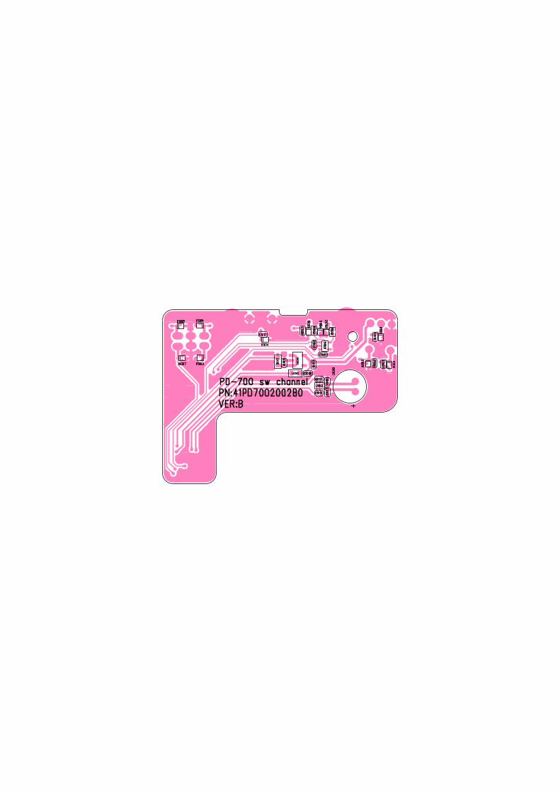


Pre-Drive2 Drive-stage Final-stage Tx/Rx Switch Low-pass Filter
Tx_VCO
AD9864
FrequencySynthesizer
Rx_VCO
Band-pass Filter1Low-Noise AmpBand-pass Filter2MixerIF FilterIF Processor IF Amp
Ref. Osc19.2MHZ
.
MOD1
MO
D2+
Freq
err
or s
hift
OMAP
4CH DAC
GPS module
BPF
HPF
ANTMicrostrip Matcher
TV1/APC
LPF
RX/TX VCO
amplifier
TO omap
TV1 /APC
From OMAP
TV1/APC
Reference OSC signal
CV Buffer
Pi Attenuator
1 2
BATT+
Stop band filter
Adapt SW
Adapt control
APC module
Low-Noise Amp
OP
Pre-driver1
RX/TX VCO buffer LPF
LPF
Pi Attenuator
1 2
CV SW
CV-read control
CV out
1
2
P i Attenuator
Pi Attenuator


LDO: 5V
LDO:5V
DC to DC 600mA
DC to DC 600mA
15mA/3V3D
RF PA 7.4V/1.6ARQA0002DNS
Vcc1 /2 2.2V-18V 210mA/Po=0.89W/7.4V
AF PA(TDA8547TS)
DVDD 1.65V-1.8V-1.95V Digital coreIOVDD 2V- 3.6V(MCLK=100M) I/O
2V- 3.6V(MCLK=50M)1.1V-2.5V External
VREF 2.3V-2.5V-2.7V Pro=2.5V SAR ADC reference voltage 1.25V Pro=1.25VVBAT 0.5V-6V Battery monitor input
Codec(TLV320AIC29IRGZR)AVDD1 3V-3.3V-3.6V Audio ADC,DAC,Reference,SAR ADCAVDD2 3V-3.3V-3.6V PLL analogBVDD 3V-4.2V Battery power supplyDRVDD 3V-3.3V-3.6V Headphone driver
Vcc (3.0V-5.5V)/1mA(No load max)
DVDD 4.5V-5V-5.5V(5V Supply) 2.7V-3V-3.3V(3 Supply)
DAC(TLV5604) No load,run clk:: Slow1.4mA/Fast 3.5mA(5V) Slow1mA/Fast 3mA(3V)AVDD 4.5V-5V-5.5V(5V Supply) 2.7V-3V-3.3V(3 Supply)Vref
VCCcp_main: Charge pump supply, 2.7V-5V(3 to 5 V);
VCCdigital: Digital supply, 2.7V-3V-3.3V;
VCCxtal : Crystal oscillator ECL/CML, 2.7V-3V-3.3V;VCCecl/cml: ECL/CML, 2.7V-3V-3.3V;
VDD 3.3V/15mA(EMIFS Bus is used 3V3D)
LCM(TFT)VLED (1*WLED 3.2±0.2V/15mA)
Vcc 2.7V-3.1V /33mA(read while write)
MCU(Nor FLASH+PsRAM))
VDD/Q 1.7V-1.8-1.95V /50mA Operation mode
SDRAM
DVDDI/O(1.71V-1.8V-AVDD)
AVDD(2.4V-2.8V-3.6V)
OMAP5912CVDDCVDD1CVDD2CVDD3CVDDRTC
Low power standby (1.05V-1.1V-1.21V)
Active mode(1.525V-1.6V-1.65V)
core logic and low voltage sections of I/Ocore logicMPU subsystem logic and memoryDSP subsystem logic and memoryRTC core logic
CVDDACVDDDLL
1.525V-1.6V-1.65V
1.525V-1.6V-1.65VAPLL provide 48MHz to peripherals(DDR)SDRAM timing
Peripheral I/O buffersMCSI2 and McBSP2 peripheral I/O buffersFlash I/F I/O buffersMMC/SD1 I/F I/O buffersMcBSP3,MCSI1,UART,USB1 I/O buffersCamera I/F and ETM I/O buffersGPIO,MPUIO,Microwire I/O buffersRTC I/ODDR/SDRAM interface I/O buffers
Low voltage range(1.65V-1.8V-1.95V)
High voltage range(2.5V-2.75Vor 3.3V-3.6V)
DVDD2Not use transceiver1.65V-1.8V-1.95V Internal USB transceiver buffersUse transceiver
3V-3.3V-3.6V
VDDF Positive supply for ADC back endVDDA Positive supply for ADC front endVDDI Positive supply for LNA and MixerVDDQ Positive supply for CLK synthesizerVDDP Positive supply for LO synthesizer charge pump
IF(AD98644) Op :17mA Std :0.01mA VDDL Positive supply for LO synthesizerVDDD Positive supply for Internal digital VDDC Positive supply for CLK synthesizerVDDH Positive supply for digital Interface
Analog voltage2.7V-3V-3.6V
Digital voltage2.7V-3V-3.6V
Interface voltage1.8V- -- -3.6V
Charge pump voltage2.7V-5V-5.5V
Vcc 3.3V/10mA LED
VCO
RX/TX
PLL(SKY72310)
3V3DRF
125uA-1000uA/5VFGU
12.5mA
0.5mA/3V3D
5mA/1V8D
3mA/1V8D
40mA/1.8VD
7.4V
Fuse2.5A/32V
Main Battery
Accelerometer(MMA7455L)
RS232(MAX3232ESE)
0.5mA/3V3A
17mA/3V3A
Vbat/2
2V5 /division
3V3ARF
20mA/3V6D
40mA/3V3D
3.5mA/5VRT
1mA/3V3ARF
5mA/5VFGU
21mA/5VFGU
3V3DRF
TX:53mA/RX:29mA
1mA/3V3D
30mA/3V3D
210MA/1V6D
5mA/3V3D
5VFGU
5VRT
3V6D
3V3A
3V3DRF
3V3D
1V6D
1V8D
16mA/3V3ARF
5VA/150mA; RX/TX/DAC
5VA-RTC/150mA; VCO
RESETRESET(MIN:800mS)
LDO1
6mA/3V3D
Vin_3V3 (3.15V-3.45V)
GPS Module (REB-1315 GSC3F/LPX)V_RTC( 2.5V-3.6V)
10uA /3V6RTC
66mA/3V3D
3V3ARF
2V5 /division
LTC1877
LDO 3V3 150mA
LDO 3V3 150mA
LDO 3V3 150mA
LDO 3V3 150mA
RESET IC
LTC1877
LDO 1V8 150mA
DVDD1DVDD3DVDD5DVDD6DVDD7DVDD8DVDD9DVDDRTC
DVDD4
230mA/7.4V/Po=0.9W
1.6A/7.4V/5W
3V3D
LDO 3V3 150mA
Back-up

5
5
4
4
3
3
2
2
1
1
D D
C C
B B
A A
BAT+
R5V
R5V
5VRT
BAT+
RX-VCO-5V 5VRT
R5V5VRT
T5V
T5V
DISCHARGE-SW-TX3
APC/TV1 1,11
PS-APC 3
ANT-GPS
9
PS-RX 3
TEM-LEV-DET-TC 13
IF8
PS-TX 3
LO1
R9083330R9083330
C91316p
C91316p
C9011100P
C9011100P
L90401nH
L90401nH
R907210KR907210K
C9039470PC9039470P
+ C905122u/10v
+ C905122u/10v
12
R9092ncR9092nc
C9067560pC9067560p
R90055.6
R90055.6
C911222pC911222p
Q9018
PBR941
Q9018
PBR941
2
31
C90881000pC90881000p
C910615pC910615p
C90591000pC90591000p
C9047470PC9047470P
R907710KR907710K
R9056120KR9056120K
R90401k
R90401k
C9040NC
C9040NC
R908456KR908456K
L9022270nHL9022270nH
L90163.3n
L90163.3n
L900418nH
L900418nH
R90303.3KR90303.3K
D90161SV329
D90161SV329
21
L9027820nH
L9027820nH L9038
330nH
L9038
330nH
R9057150K-FR9057150K-F
L90344P
L90344P
C91155P
C91155P
C9034
470P
C9034
470P
C901410pC901410p
C9140NC
C9140NC
D9007BA277D9007BA277
12
C91096P
C91096P
C9099
10p
C9099
10p
C90093P
C90093P
R90081.5KR90081.5K
R90973.3K
R90973.3K
C90490.1uC90490.1u
C90931000PC90931000P
Q90042SC4988Q90042SC4988
1
23
R9015330
R9015330
R90473.9KR90473.9K
C911827p
C911827p
C9090
0.01u
C9090
0.01u
C9062NCC9062NC
C91324PC91324P
C91078pC91078p
DTC114EEQ9008
DTC114EEQ9008
3
1
2
R9086NC
R9086NC
R90963.3KR90963.3K
C90328p
C90328p
C90440.01uC90440.01u
C90460.1uC90460.1u
C91335P
C91335P
R9068
3.3K
R9068
3.3K
C90380.1uC90380.1u
C9081470PC9081470P
DTC114EEQ9007
DTC114EEQ9007
3
1
2
R9029330
R9029330
D9005BA277D9005BA277
12
R9011100
R9011100
D9015
1SV329
D9015
1SV329
21
C90430.1uC90430.1u
TP9001APC-outTP9001APC-out
1
R9046470K-FR9046470K-F
C91298P
C91298P
L900318nH
L900318nH
Q9019
EMD22
Q9019
EMD22
1
2
4 3
6
5
L9026
100n
L9026
100n
C90634700pC90634700p
TP9004TPTP9004TP
R90953.3KR90953.3K
R907410kR907410k
C9098
470pF
C9098
470pF
C912227pC912227p
L901015nL901015n
R90785.6KR90785.6K
R90581M-FR90581M-F
R9025270R9025270
C9110
0.01u
C9110
0.01u
C9036
1000pF
C9036
1000pF
L90111uL90111u
D9001
1SV329
D9001
1SV329
21
R90331k
R90331k
C9045470P
C9045470P
R9093ncR9093nc
R9028270R9028270
L9028
22n
L9028
22n
R9012100R9012100
R9091ncR9091nc
C907912pC907912p
C90910.1u
C90910.1u
R9039100R9039100
C90308p
C90308p
C9005NCC9005NC
C9128
5P
C9128
5P
L9012220nL9012220n
R90433.3K
R90433.3K
C9042470PC9042470P
L9039
1000P
L9039
1000P
L903
65T
L903
65T
C9104
0.1U
C9104
0.1UT9001XFMRT9001XFMR
61 2
43
R9016150R9016150
D9002
1SS356
D9002
1SS356
1 2
D9017HSMS-2827
D9017HSMS-2827
1
32
4
L9029NCL9029NC
C9002100PC9002100P
R90940
R90940
R90351k
R90351k
Q9001AT-41511
Q9001AT-41511 1
243
C907710p
C907710p
C9119NCC9119NC
R908110KR908110K
U9003
LM45
U9003
LM45
+VS1VO 2
GND3
L90355T
L90355T
R90661.5kR90661.5k
R902147
R902147
R9050
47K
R9050
47K
C90314.7PC90314.7P
L900256n
L900256n
L901815n(high Q) L901815n(high Q)
R9018680R9018680
C9103
1000P
C9103
1000P
C9019
9P
C9019
9P
Q9005RD01MUS2
Q9005RD01MUS2
1
32
R90451M-F
R90451M-F
C910510pC910510p
L902556NH
L902556NH
R9085100KR9085100K
R903610k
R903610k
Q9017
PBR941
Q9017
PBR9412
31
C90268p
C90268p
R90133.3K
R90133.3K
C9136
5P
C9136
5P
R9069
0R
R9069
0R
C9135
5P
C9135
5P
R900933
R900933
R90233.9K
R90233.9K
L9015BLM15PD121SN1
L9015BLM15PD121SN1
12
R9017100R9017100
R907310KR907310K
C90641000pC90641000p
C91163pC91163p
Q9003RD07MUS2B
Q9003RD07MUS2B
1
32
C90860.1uC90860.1u
C902043p
C902043p
C9029470PC9029470P
R90540.39R90540.39
C90891000PC90891000P
R90414.7KR90414.7K
C9097
0.1u
C9097
0.1u
C9069470PC9069470P
C90077P
C90077P
R9048150K-FR9048150K-F
L901718n(high Q)L901718n(high Q)
C9073nc
C9073nc
C9017
NC
C9017
NC
C90410.1uC90410.1u
L900182n
L900182n
R9100100PR9100100P
C9121
1000P
C9121
1000PR90895.6kR90895.6k
C9050NCC9050NC
C90011000PC90011000P
R900782
R900782
Q90212SA1832
Q90212SA1832
1
23
R907610KR907610K
C91208PC91208P
C90155P
C90155P
C9006NC
C9006NC
C9070
NC
C9070
NC
R9026NC
R9026NC
C9139NC
C9139NC
C91347.5P
C91347.5P
R90278.2kR90278.2k
Q9020
EMD22
Q9020
EMD22
1
2
43
6
5
L900915n
L900915n
C90651500pC90651500p
D9010EDZTE616.8BD9010
EDZTE616.8B
12
C91016pC91016p
R900247KR900247K
C91116p
C91116p
R9034NCR9034NC
R906347KR906347K
C914147pFC914147pF
C902712PC902712P
C9052
1uF
C9052
1uF
R908020PR908020P
R90983.3K
R90983.3K
R902222R902222
L90078.2nL90078.2n
C90870.01u
C90870.01u
L90335T
L90335T
C9054
NC
C9054
NC
R90550.39R90550.39
C9022
NC
C9022
NCC9024
6pC9024
6p
R90246.8KR90246.8K
C90041.5pC90041.5p
C91380.01u
C91380.01u
R9099100PR9099100P
R907933KR907933K
D9012
1SV329
D9012
1SV329
21
C9058NC
C9058NC
T9002
XFMR
T9002
XFMR
612
43
C90951uFC90951uF
Q90062SA1745
Q90062SA1745
1
2 3
R9001270
R9001270
R9067
6.8k
R9067
6.8k
C90710.1uC90710.1u
C9033470P
C9033470P
L9020BLM15PD121SN1L9020
BLM15PD121SN1
12
C9016NCC9016NC
R9031NC
R9031NC
C907820pC907820p
L9024330N
L9024330N
R9042NC
R9042NC
C9074nc
C9074nc
L90068.2nL90068.2n
L9013
18nH
L9013
18nH
R90381kR90381k
C9053NCC9053NC
C90030.75pC90030.75p
U9002
NJM2904V
U9002
NJM2904V
A OUTPUT1A -INPUT2A +INPUT3
V+ 8
B +INPUT 5B -INPUT 6B OUTPUT 7
GND4
C90287p
C90287p L9031
NCL9031NC
R90044.4nHR90044.4nH
C91246pC91246p
C91231000PC91231000P
C90851000PC90851000P
R9037NC
R9037NC
L9014BLM18SG121TN1L9014BLM18SG121TN1
12
R9003270
R9003270
D9006
BA277
D9006
BA277
12
L900518nHL900518nH
R902010K
R902010K
C9075470p
C9075470p
ANT1ANT1
1
C91175p
C91175p
R90530.39
R90530.39
D9013
HSM88AS
D9013
HSM88AS
321
C9012nc
C9012nc
D9014
1SV329
D9014
1SV329
21
L9032
220n
L9032
220n
L900847nHL900847nH
C9130ncC9130nc
R9059470K-FR9059470K-F
C903515PC903515P
R9071330R9071330
C91002pC91002p
C9008nc
C9008nc
C9096470pFC9096470pFC9092
0.1uFC90920.1uF
C91376pC91376p
GND GND
INOUT
Z900173.35M
GND GND
INOUT
Z900173.35M
1
23
4
56
C9060
1000P
C9060
1000P
C90570.1uC90570.1u
L903
75T
L903
75T
C9126NCC9126NC
R90194.7KR90194.7K
R900610kR900610k
C90212.4P
C90212.4P
C90800.1uC90800.1u
R9032NC
R9032NC
C9094NCC9094NC
D9008HVC131D9008HVC131
12
C90660.01uC90660.01u
R909010KR909010K
C9048470PC9048470P
C902510PC902510P
C9037470PC9037470P
L90302.7nHL90302.7nH
R9014ncR9014nc
Q90022SC3356Q90022SC3356
2
31
C90236p
C90236p
C91138pC91138p
C90611000PC90611000P
TP9003
TP
TP9003
TP
C9018470PC9018
470P
R907551R907551
C91145.6K
C91145.6K
D9011DAN222
D9011DAN222
1
23
C9013470PC9013470P

5 4 3 2 1
D
C
B
A A
AD
C-IN
ADC-IN
PD-CODEC
MICBIAS--HEDA
F-C
OD
EC
-IN
AF-CODEC-OUT
AF-
CO
DE
C-O
UT
MICBIAS--HND
AF-CODEC-IN
1V8D
3V3D
3V3A
3V3A
3V3A
INT-BAT+
IIS-W
CLK
-CO
DE
C5
IIS-B
LCK
-CO
DE
C5
IIS-D
I-CO
DE
C5
DA
V-C
OD
EC
3
VOL7
CV-ADC1
AF-OUT- 12
TEM-LEV-DET-TC14EXT-MIC- 7
EXT-MIC+ 7uW
-CLK
-CO
DE
C5
uW-C
S3-
CO
DE
C5
uW-S
DO
-CO
DE
C5
uW-S
DI-C
OD
EC
5
CLK
-CO
DE
C2
IIS-D
O-C
OD
EC
5
RESET-CODEC3
SEL1-ADC 3
SEL2-ADC 3
INT-MIC+780 7
INT-MIC-780 7
TONE-CODEC 3
SEL-MIC 3
AF-CODEC-TO-50PIN
AF-50PIN-TO-CODEC
AF-OUT+ 12
Vref=2.5V
C838470PC838470P
TP820AF-OUTTP820AF-OUT
1
U820
NLAS4783BMN1R2G
U820
NLAS4783BMN1R2G
EN
AB
LE4
X010X111X12Z11Z2Z03
GN
D6
NC
5
Vcc
14
Y0 16Y1 15
Y 13
A 9B 8C 7
C822
0.01u
C822
0.01u
L828BLM18AG601SN1
L828BLM18AG601SN1
C845
470P
C845
470P
L821BLM15PD121SN1
L821BLM15PD121SN1
R82310KR82310K
L823BLM18AG601SN1
L823BLM18AG601SN1
C8370.01uC8370.01u
C8210.22uC8210.22u
R833
2K
R833
2K
R83033K-FR83033K-F
C8330.1uC8330.1u
C849
470P
C849
470P
L827BLM18AG601SN1
L827BLM18AG601SN1
TP823GNDTP823GND
1
L820
10
L820
10
C848
470P
C848
470P
R826 47K-FR826 47K-F
C857
470P
C857
470P
R824 15K-FR824 15K-F
C8520.1uC8520.1u
C842
470P
C842
470P
R838 10KR838 10K
TP821TP821 1TLV320AIC29IRGZR
U821
TLV320AIC29IRGZR
U821IOVDD1PWR_DN2RESET3GPIO24GPIO15AVDD26AVSS27AVDD18NC9NC10NC11NC12
AV
SS
113
VR
EF
14V
BA
T15
AU
X2
16A
UX
117
BU
ZZ_I
N/C
P_I
NN
18C
P_O
UTP
19C
P_I
NP
20M
ICIN
_HN
D21
MIC
BIA
S_H
ND
22M
ICIN
_HE
D23
MIC
BIA
S_H
ED
24
MIC_DET 25OUT32N 26SPK1 27SPK2 28DRVDD 29SPKFC 30VGND/CP_OUTN 31DRVSS1 32OUT8N 33BVDD 34OUT8P 35DRVSS2 36
DA
V37
SS
38M
OS
I39
MIS
O40
SC
LK41
MC
LK42
SD
OU
T43
SD
IN44
WC
LK45
BC
LK46
DV
DD
47D
VS
S48
T-P
AD
49C828
2.2u/10VC828
2.2u/10V
C8341uC8341u R829 470KR829 470K
C8430.1uC8430.1u
C858
3900P
C858
3900P
R841 10KR841 10K
C851470PC851470P
C853470P
C853470P
C8401uC8401u
L822BLM15PD121SN1
L822BLM15PD121SN1
C8360.1uC8360.1u
C856
470P
C856
470P
C827
0.01u
C827
0.01u
TP822MIC+TP822MIC+
1
R825 2KR825 2K
C824
0.22u
C824
0.22u
R820
2K
R820
2K
R832
2K
R832
2K
C8500.1uC8500.1u
R821
100
R821
100
C8321uC8321u
C8471uC8471u
C835470PC835470P
C825
2.2u/10V
C825
2.2u/10V
C831
1u
C831
1u
R828 15K-FR828 15K-F
C846
470P
C846
470P
C839
0.1u
C839
0.1u
C826
0.01u
C826
0.01u

5 4 3 2 1
D
C
B
A A
BAT+
INT-BAT+
Mode-AMP3
SEL-SPK3
AF-OUt-13
AF-OUT+13
IN-SPK+ 7
IN-SPK- 7
EXT-SPK- 7
EXT-SPK+ 7
C8010.1uC8010.1u
C810
0.1u
C810
0.1u
R81110KR81110K
R803150KR803150K
L801L801
C806220pC806220p
R80610R80610
R805
10K
R805
10K
C8090.1uC8090.1u
L805L805
U801
TDA8547TS
U801
TDA8547TS
VC
C1
20
VC
C2
11
IN1-17
IN1+16 OUT1- 18
OUT1+ 3IN2-14
IN2+15
SVRR5
MODE4SELECT6
GN
D1
1G
ND
210
OUT2+ 8
OUT2- 13
NC
2N
C7
NC
9N
C12
NC
19
TP801TP801
1
L803L803
C805220pC805220p
TP802TP802
1
R80110R80110
R804
10K
R804
10K
L804L804
L802
BLM18PG181SN1
L802
BLM18PG181SN1
R807
20K
R807
20K
R802150KR802150K
C8190.01uC819
0.01u
C802
10u/10V
C802
10u/10V
R814150KR814150K
C8083900pC808
3900p
C804
270P
C804
270P
DTC114EEQ802
DTC114EEQ802
3
1
2
R81210KR81210K
C8203900pC820
3900p
C816
1u/16V
C816
1u/16V
DTC114EEQ801
DTC114EEQ801
3
1
2
R813150KR813150K
C8133900pC813
3900p
C8233900pC8233900p
C803
0.22u
C803
0.22u
C812
0.1u
C812
0.1u

5 4 3 2 1
D
C
B
A A
LOAD-DAC
PD-DAC
5VRT
3V3DRF
MOD-XO 1
APC/TV1 1,14
MOD-VCO 1
MCBSP2-DX-DAC5MCBSP2-CLKX-DAC5MCBSP2-FSX-DAC5
TO VCO
TO VCTCXO
TP702APC/TV1TP702APC/TV1
1
C704470pC704470p
R71410kR71410k
R707
33kR707
33k
R713100R713100
R705 10K-FR705 10K-F
R712BLM15AG121SN1
R712BLM15AG121SN11 2
R701 1KR701 1K
C708100pC708100p
C703470PC703470P
U701TLV5614IPWU701TLV5614IPW
DV
DD
1P
D2
LDA
C3
DIN
4S
CLK
5C
S6
FS7
DG
ND
8R
EFI
NC
D10
AG
ND
9
RE
FIN
AB
15O
UTA
14O
UTB
13O
UTC
12O
UTD
11
AV
DD
16
C7011u/10vC7011u/10v
C7051000PC7051000P
R71110kR71110k
C7061uC7061u
R704 100R704 100
R709
100k
R709
100k
C7100.1uC7100.1u
C712
1u
C712
1u
C7111u
C7111u
R70268kR70268k
R706 10K-FR706 10K-F
R710100kR710100k
TP701MOD2TP701MOD2
1
L702
BLM15AG121SN1
L702
BLM15AG121SN11 2
C7071uC7071u
C709100pC709100p

5
5
4
4
3
3
2
2
1
1
D D
C C
B B
A A
POWER-SW+
POWER-SW+
POWER-SW+
3V3D
1V6D
5VRT
3V3D
3V6D
5VFGU
BAT+
3V6D
1V8D
3V3A
BAT+ EXT-BAT+
3V3ARFBAT+
3V3GPS
3V3DRF
3V3DRF
BAT+ INT-BAT+
3V3DRF
PS-GPS3
PWR-RESET2
PWR-SW+ 6,7
PWR-SW- 6,7,12,13
EXT-PWR 3
POWER-CTL 3
POWER-KEY-DET 3
POWER-CTL 3
Maximal current 500mA
add:L617、C659、C651
del:TP601
C676
0.22uF 10V
C676
0.22uF 10V C6012.2uFC6012.2uF
R628 47KR628 47K
C6503900PC6503900P
C6040.1uF/16V
C6040.1uF/16V
C6780.22uF 10VC678
0.22uF 10V
C6830.22uFC6830.22uF
C612
NC
C612
NC
U607TPS3808G33QDBVRQ1
U607TPS3808G33QDBVRQ1
RESET1
MR3 GND2Ct 4
VDD 6SENSE 5
U608RP102N331B
U608RP102N331B
VDD1GND2CE3 NC 4
VOUT 5
C616100pFC616100pF
C620100pF/16V
C620100pF/16V
C6602.2uFC6602.2uF
D602D602
21
L601
BLM18PG181SN1
L601
BLM18PG181SN1
C619C619
C6710.1uFC6710.1uF
L613L613
R632 1KR632 1K
C6843900PC6843900P
L616L616
TP6041.8VTP6041.8V
1
C606
2.2uF
C606
2.2uF
U605
TK11250CM
U605
TK11250CM
ON
/OFF
1G
ND
2N
P(V
RE
F)3
VIN
6G
ND
5V
OU
T4
C679
0.1uF/16V
C679
0.1uF/16V
D601D601
12
U601U601
RUN1
SYNC7
VFB3
PLLPF8
ITH2 GN
D4
VIN
6
SW 5 C685470PC685470P
C6873900PC6873900P
F602
1206L050-C
F602
1206L050-C
1 2
C6400.22UF 10V
C6400.22UF 10V
C6412.2uFC6412.2uF
C6242.2uFC6242.2uF
U612RP102N331B
U612RP102N331B
VDD1GND2CE3 NC 4
VOUT 5
C6081uFC6081uF
+ C63747u
+ C63747u
12
U609RP102N331B
U609RP102N331B
VDD1GND2CE3 NC 4
VOUT 5
U611U611
RUN1
SYNC7
VFB3
PLLPF8
ITH2 GN
D4
VIN
6
SW 5
Q605
SI1013R (SI2307BDS)
Q605
SI1013R (SI2307BDS)
1
23
C6250.1uFC6250.1uF
R625
100K
R625
100K
D604DAN222
D604DAN222
1
23
C603NC*4.7uF/16V
C603NC*4.7uF/16V
C6180.1uF/16VC6180.1uF/16V
C636C636
11 2 233
L610L610
C617
0.1uF/16V
C617
0.1uF/16V
C681
470P
C681
470P
C6863900PC6863900P
C680
470P
C680
470P
L612
BLM18PG181SN1
L612
BLM18PG181SN1
C6580.1uF/16V
C6580.1uF/16V
Q608
2SK1824
Q608
2SK18242
31
C639
0.1uF
C639
0.1uF
C6294.7uF/16V
C6294.7uF/16V
C659
0.1uF
C659
0.1uF
C611
NC
C611
NC
L611
BLM18PG181SN1
L611
BLM18PG181SN1
R627 47KR627 47K
C657C657
11 2 233
C654C654
11 2 233
Q603Q603
1
32
C6702.2uFC6702.2uF
R620
100K
R620
100K
L614L614
C6150.1u/16VC615
0.1u/16V
C602100pF/16V
C602100pF/16V
C6492.2uFC6492.2uF
P606P606
1
C646C646
11 2 233
C6300.1uF/16V
C6300.1uF/16V
C6623900PC6623900P
C6350.1uFC6350.1uF
U604
TK11250CM
U604
TK11250CM
ON
/OFF
1G
ND
2N
P(V
RE
F)3
VIN
6G
ND
5V
OU
T4
C682
0.1uF/16V
C682
0.1uF/16V
Q606
SI1013R
Q606
SI1013R
1
23
C609
NC
C609
NC
C6280.22UF 10V
C6280.22UF 10V
R622R622
Q607
2SK1824
Q607
2SK18242
31
C6383900P
C6383900P
C651
0.01uF
C651
0.01uF
C613NC
C613NC
R631 15KR631 15K
C656
0.1uF
C656
0.1uF
R629 2.7KR629 2.7K
C668
0.01uF
C668
0.01uF
C666
3900p
C666
3900p
L615L615
TP6033.6VTP6033.6V
1
+ C66547u
+ C66547u
12
R630 47KR630 47K
C652470pFC652470pF
L603
BLM18PG181SN1
L603
BLM18PG181SN1
R615
NC
R615
NC
L602BLM18PG181SN1
L602BLM18PG181SN1
R626
100K
R626
100K
L606
BLM18PG181SN1
L606
BLM18PG181SN1
C627C627
11 2 233
J601
PD-700/BATB
J601
PD-700/BATB
12345
C645220P/50V
C645220P/50V
R607 10R607 10
R633
100K
R633
100K
R611
10K
R611
10K
L617
BLM18PG181SN1
L617
BLM18PG181SN1
C6420.1uFC6420.1uF
P608P608
1
P609P609
1
R623
100K-F
R623
100K-F
U603NC
U603NC
VDD1GND2CE3 NC 4
VOUT 5
C6145.6pFC6145.6pF
R624
100K
R624
100K
R612 1KR612 1K
C6532.2uFC6532.2uF
R62147KR62147K
L605BLM18PG181SN1
L605BLM18PG181SN1
R618130K-FR618130K-F
C647
0.01uF
C647
0.01uF
P610P610
1C674
220P/50VC674
220P/50V
Q604
2SK1824
Q604
2SK18242
31
TP602RESETTP602RESET
1
C6231uF/25VC6231uF/25V
TP6051.6VTP6051.6V
1
C688
0.1uF
C688
0.1uF
C6051uF/25VC605
1uF/25V
C6550.22UF 10V
C6550.22UF 10V
L604
NC
L604
NC
C672
20pF/50V
C672
20pF/50V
R617
470K-F
R617
470K-F
C610NCC610NC
C6214.7uF/16V
C6214.7uF/16V
L607L607
C6771uFC677
1uF
C669
1uF
C669
1uF
U606RP102N331B
U606RP102N331B
VDD1GND2CE3 NC 4
VOUT 5
R614R614
C648
1uF
C648
1uF
R613 1KR613 1K
C667C667
11 2 233
U610RP102N181D
U610RP102N181D
VDD1GND2CE3 NC 4
VOUT 5
F601
2.5A-32V
F601
2.5A-32V
1 2
L609
BLM18PG181SN1
L609
BLM18PG181SN1
C6260.1uF/16VC6260.1uF/16V
C644
20pF/50V
C644
20pF/50V
C663470pFC663470pF
R601
91K-F
R601
91K-F
P607P607
1
C661C661
11 2 233
C6220.1uF/16V
C6220.1uF/16V
C607
0.1uF
C607
0.1uF

5
5
4
4
3
3
2
2
1
1
D D
C C
B B
A A
SYNCB-IF
5VFGU
3V3DRF
3V3A
CLK-IF/PLL 1
CLK-OMAP/IF 2
IF14
PS-2LOC 3
SPI-DIN-IF 5
SPI-SCK-IF 5SPI-DOUT-IF 5SPI-CS2-IF 5
MCBSP2-FSR-IF 5
MCBSP2-CLKR-IF 5MCBSP2-DR-IF 5
TP413FERCLK
TP413FERCLK
1
R405 10KR405 10K
C464
0.1u
C464
0.1u
C4470.01uC4470.01u
D4021SV305
D4021SV3052
1
C44339PC44339P
C427
220p
C427
220p
C4312200pC4312200p
R4078.2KR4078.2K
Q4012SC4617
Q4012SC4617
2
31
R4094.7KR4094.7K
L403 BLM15AG121SN1L403 BLM15AG121SN11 2
C4650.1uC4650.1u
C451NCC451NC
C44833pC44833p
C428100PC428100P
C46133pC46133p
C4570.01uC4570.01u
C421ncC421nc
R412100kR412100k
C4490.01uC4490.01u
C435
0.1u
C435
0.1u
C429100PC429100P
L405
BLM15AG121SN1
L405
BLM15AG121SN1
1 2
C466
0.1u
C466
0.1u
C469
270P
C469
270P
R411390R411390
L4136.8UHL4136.8UH
C4400.01uC4400.01u
C45818pC45818p
C438100PC438100P
C450
0.012u
C450
0.012u
C43222pC43222p
TP403GNDTP403GND
1
C4527PC4527P
C470
270P
C470
270P
R403150RR403150R
R41010kR41010k
R408100R408100
C467
2.2u/10v
C467
2.2u/10v
L410BLM18AG601SN1
L410BLM18AG601SN1
C453 0.01uC453 0.01u
C441
0.1u
C441
0.1u
C459470PC459470P
C4620.1uC4620.1u
C4340.1uC4340.1u
R414 2.7kR414 2.7k
C471
270P
C471
270P
C4375600PC4375600P
C4722.2uFC4722.2uF
C42518pC42518p
R416820RR416820R
TP404CV2TP404CV2
1
C4220.1uC4220.1u
C42012PC42012P
R404
1.2KR404
1.2K
TP4012FLOTP4012FLO
1
R40151R40151
C439100PC439100P
R4131.8kR4131.8k
D401
HVC350B
D401
HVC350B21
C4540.01uC4540.01u
R4061KR4061K
C444470PC444470P
C4260.01uC4260.01u
L402
270n
L402
270n
L411 3.3uL411 3.3u
C423
1u
C423
1u
R415
10K
R415
10K
+C4680.68u/10v+
C4680.68u/10v
12
L412 BLM15AG121SN1L412 BLM15AG121SN11 2
C436
0.01u
C436
0.01u
C455
3300PC455
3300P
L407BLM15PD121SN1
L407BLM15PD121SN1
1 2
U401
AD9864
U401
AD9864
MXOP1MXON2GNDF3IF2N4IF2P5VDDF6GCP7GCN8VDDA9GNDA10VREFP11VREFN12
RR
EF13
VDD
Q14
IOU
TC15
GN
DQ
16VD
DC
17G
ND
C18
CLK
P19
CLK
N20
GN
DS
21G
ND
D22
PC23
PD24
PE 25VDDD 26VDDH 27CLKOUT 28DOUTA 29DOUTB 30FS 31GNDH 32SYNCB 33GNDS 34FREF 35GNDL 36
GN
DP
37IO
UTL
38VD
DP
39VD
DL
40C
XVM
41LO
N42
LOP
43C
XVL
44G
ND
I45
CXI
F46
IFIN
47VD
DI
48PRPAD 49
R40210kR40210k
C430
0.1u
C430
0.1u
C4563.6pC4563.6p
C46030pC46030p
Q402
UMC4N
Q402
UMC4N
1
2
34
5
C4420.01uC4420.01u
L40410uL40410u
Q4032SC3356
Q4032SC3356
2
31
L409
470nHL409
470nH
C4450.1uC4450.1u
L4084.7uL4084.7u
C4630.22uC463
0.22u
L40110uL40110u
C433
0.1u
C433
0.1u
L406220n(HQ)L406220n(HQ)
TP402IF
TP402IF
1
C4460.1uC4460.1u

5
5
4
4
3
3
2
2
1
1
D D
C C
B B
A A
MOT+
LED-K-LCD
IMO
LED-K-LCD
LED-K-KEY
LED-K-KEY
LED1LED2
PTT-KEY
LED1LED2
MOT-
3V3DRF
3V3D
3V3A
3V6D
3V3D3V6D
EXT-BAT+
VFLASH
3V3D
3V3DRF
CH1 3
CH2 3CH8 3
LED-IND1 3
INT-PTT 3
LED-IND2 3
CH4 3
UART1-RX-OPT/PS5,6
UART1-TX-OPT/PS5,6
EMERGENCY 3
KB-C1 5
MOTOR-CTL 3
IIC-SCL-Acce 5
KB-R0 5
KB-C0 5
IIC-SDA-Acce 5
Acce-INT1 3
PWR-SW+ 6,10PWR-SW- 6,10,12,13
VOL 13
KB-C05KB-C15KB-C25KB-C35KB-C45
/RST-OUT3/CS2-LCD 4M-A1 4
M-D2 4M-D34M-D4 4
M-D14 M-D0 4
/WE4 /OE 4
M-D74 M-D6 4M-D54
M-D134 M-D14 4M-D154
M-D8 4M-D94M-D10 4M-D114
M-D12 4
LED-LCD-BL 3 LED-KEY 3
USB-D- 5,6USB-D+ 5,6
EXT-SPK+ 12
EXT-SPK- 12
MCBSP3-DX-OPT 5
MCBSP3-DR-OPT 5MCBSP3-CLK-OPT 5
MCBSP3-FSX-OPT 5
UART3-RTS/IO29-OPT5UART3-CTS/IO30-OPT5
UART3-TX-OPT5UART3-RX-OPT5
IO1-OPT3IO2-OPT3IO3-OPT3
IN-SPK-12
IN-SPK+12
IO5-OPT3IO4-OPT3
INT-MIC-780 13INT-MIC+780 13
EXT-MIC-13
EXT-MIC+13
SEL2-Accessory 3SEL3-Accessory 3
EMERGENCY 3KB-R1 5KB-R2 5KB-R3 5KB-R4 5
SEL1-Accessory 3,13
IO-TD-TEST3
AF-CODEC-TO-50PINAF-50PIN-TO-CODEC
EXT-PTT 3
IIC-SCL-Acce 5
IIC-SDA-Acce 5
IIC-INT 5
IIC-SCL-Acce 5IIC-SDA-Acce 5
add:C325、C326
U317U317
X1 A1X2 A2X3 A3X4 A4X5 A5X6 A6
Y1C1Y2C2Y3C3Y4C4Y5C5Y6C6
GN
D1
B1
GN
D2
B2
GN
D3
B3
C315
470p
C315
470p
D309D3092 1
D318D3181
543 2
6
Q310
BSH103
Q310
BSH103
1
32
U318U318
X1 A1X2 A2X3 A3X4 A4X5 A5X6 A6
Y1C1Y2C2Y3C3Y4C4Y5C5Y6C6
GN
D1
B1
GN
D2
B2
GN
D3
B3
R323
2.2K
R323
2.2K
J313
JST SM02B-SRSS-TB(LF)
J313
JST SM02B-SRSS-TB(LF)
12
D310D3102 1
C319
100k
C319
100k
C331
470P
C331
470P
C322
270P
C322
270P
C334270pC334270p
L305BLM18AG601SN1
L305BLM18AG601SN1
U313U313
X1 A1X2 A2X3 A3X4 A4X5 A5X6 A6
Y1C1Y2C2Y3C3Y4C4Y5C5Y6C6
GN
D1
B1
GN
D2
B2
GN
D3
B3
U314U314
X1A1X2A2X3A3X4A4X5A5X6A6
Y1 C1Y2 C2Y3 C3Y4 C4Y5 C5Y6 C6
GN
D1
B1
GN
D2
B2
GN
D3
B3
C335
470P
C335
470P
P312P312 1
J1601
AXK6F50347YG
J1601
AXK6F50347YG
1234567891011121314151617181920212223242526272829303132333435363738394041424344454647484950
D302
1N4148WS
D302
1N4148WS
12
U316U316
X1 A1X2 A2X3 A3X4 A4X5 A5X6 A6
Y1C1Y2C2Y3C3Y4C4Y5C5Y6C6
GN
D1
B1
GN
D2
B2
GN
D3
B3
L303BLM18PG181SN1
L303BLM18PG181SN1
R331R331
R330R330
R321
3.01
R321
3.01
R324 33R324 33
L304BLM18AG601SN1
L304BLM18AG601SN1
J311
DF12E(3.0)-30DP-0.5V(81)
J311
DF12E(3.0)-30DP-0.5V(81)
1 23 45 67 89 10
11 1213 1415 1617 1819 2021 2223 2425 2627 2829 30
P314P314 1
C318
0.1u
C318
0.1u
R329R329
U312U312
X1A1X2A2X3A3X4A4X5A5X6A6
Y1 C1Y2 C2Y3 C3Y4 C4Y5 C5Y6 C6
GN
D1
B1
GN
D2
B2
GN
D3
B3
C324
470P
C324
470P
C332
470P
C332
470P
C321
270P
C321
270P
D305D305
2 1
C313
470p
C313
470p
R325 33R325 33
C3100.1uC3100.1u
U320U320
X1A1X2A2X3A3X4A4X5A5X6A6
Y1 C1Y2 C2Y3 C3Y4 C4Y5 C5Y6 C6
GN
D1
B1
GN
D2
B2
GN
D3
B3
R318100KR318100K
D306D306
2 1
P313P313 1
U310
NC*MMA7455L
U310
NC*MMA7455L
DVdd_IO1GND2NC3IADDR04GND15AVdd6CS7 INT1/DRDY 8INT2 9NC1 10RFU 11SDO 12SDA/SDI/SDO 13SLC/SPC 14
P311P311 1
R317 10KR317 10K
D304D304
21
C323
1u
C323
1u
C333
470P
C333
470P
R3153.3KR3153.3K
C3141uC3141u
R326 33R326 33
Q313
BSH103
Q313
BSH1031
32
R316 10KR316 10K
R3143.3KR3143.3K
C3121u
C3121u
C336
470P
C336
470P
R322
2.2K
R322
2.2K
DTC114EEQ312
DTC114EEQ312
3
1
2
U315U315
X1 A1X2 A2X3 A3X4 A4X5 A5X6 A6
Y1C1Y2C2Y3C3Y4C4Y5C5Y6C6
GN
D1
B1
GN
D2
B2
GN
D3
B3
J821
AXK5F16547YG
J821
AXK5F16547YG
12345678910111213141516
L302BLM18AG601SN1
L302BLM18AG601SN1
TP301TP301
1
D307D30721
U321U321
X1A1X2A2X3A3X4A4X5A5X6A6
Y1 C1Y2 C2Y3 C3Y4 C4Y5 C5Y6 C6
GN
D1
B1
GN
D2
B2
GN
D3
B3
U319U319X1A1 X2A2 X3A3 X4A4 X5A5 X6A6
Y1 C1Y2 C2Y3 C3Y4 C4Y5 C5Y6 C6
GN
D1
B1
GN
D2
B2
GN
D3
B3
C326
270p
C326
270p
C320
470p
C320
470p
C317
470p
C317
470p
C316
470p
C316
470p
P310P310 1
U322U322
X1A1X2A2X3A3X4A4X5A5X6A6
Y1 C1Y2 C2Y3 C3Y4 C4Y5 C5Y6 C6
GN
D1
B1
GN
D2
B2
GN
D3
B3
D308D30821
D303D303
21
C325
270p
C325
270p
C311
0.1u
C311
0.1u

5
5
4
4
3
3
2
2
1
1
D D
C C
B B
A A
3V3D
3V3D
3V3D
MCBSP3-DX-OPT7MCBSP3-DR-OPT7
KB-R2 7
IIC-SDA-Acce7
SPI-DIN-IF8
UART3-RTS/IO29-OPT 7
KB-R3 7
uW-SDO-CODEC13
UART3-CTS/IO30-OPT 7
KB-R0 7
SPI-SCK-IF8
uW-SDI-CODEC13
UART3-TX-OPT 7
IIS-BLCK-CODEC13
KB-C1 7
UART3-RX-OPT 7
SPI-DOUT-IF8
MCBSP3-CLK-OPT7
IIS-WCLK-CODEC13
KB-C2 7
MCBSP3-FSX-OPT7
KB-C3 7
IIS-DI-CODEC13
KB-C4 7
IIS-DO-CODEC13
IIC-SCL-Acce7
KB-R4 7
KB-C0 7
KB-R1 7
EMU1 6
TDO 6
/TRST 6TMS 6TDI 6
RTCK 6TCK 6EMU0 6
UART2-RX-GPS 9UART2-TX-GPS 9
USB-D+ 6,7USB-D- 6,7
MCBSP2-CLKR-IF8MCBSP2-FSR-IF8MCBSP2-DR-IF8
MCBSP2-CLKX-DAC11MCBSP2-FSX-DAC11MCBSP2-DX-DAC11
MCSI-CS-PLL1MCSI-CLK-PLL1
MCSI-DO-PLL1
SPI-CS2-IF8
uW-CLK-CODEC13uW-CS3-CODEC13 UART1-TX-OPT/PS 6,7
UART1-RX-OPT/PS 6,7
C260
560P
C260
560P
C270
270P
C270
270P
R25810KR25810K
C269
470P
C269
470P
C272
47P
C272
47P
R226 100R226 100
C261
560P
C261
560P
TP269TP269
1
C271
47P
C271
47P
TP264TP264
1R259 33R259 33
TP255TP255
1
C299
470P
C299
470P
R25610KR25610K
C262
270P
C262
270P
C293470PC293470P
TP263TP263
1
R255 33R255 33
TP260TP260
1
C286
47P
C286
47P
C273
47P
C273
47P
C263
470P
C263
470P
RN26122K*2RN26122K*2
1 234
C279
47P
C279
47P
C294470PC294470P
R222 100R222 100
C266470PC266470P
R262
15K
R262
15K
C291270PC291270P
RN25610K*4RN25610K*4
1 2 3 45678
C265
100P
C265
100P
R224 100R224 100
R261
15K
R261
15K
R223 33R223 33
C264
470P
C264
470P
C296
470P
C296
470P
OMAP5912ZZG-1U201B
OMAP5912ZZG-1U201B
MCBSP1.CLKX/GPIO54G21 MCBSP1.FSX/GPIO53H15
MCBSP1.DX/GPIO52H18MCBSP1.DR/GPIO51H20
SPIF.DIN/GPIO47/uWIRE.SDIU18 SPIF.DOUT/GPIO46/uWIRE.SDOW21
MCBSP3.DX/GPIO43/MCSI1.CLKP14 MCBSP3.CLKX/GPIO42W16
MCSI1.DOUT/GPIO18W14
MCBSP3.FSX/GPIO12/TIMER.EXTCLKN18
MCSI1.SYNC/GPIO9W8 MCSI1.CLK/GPIO7M15
SPIF.CS2/MPUIO4/uWIRE.CS2/LED2T19SPIF.SCK/MPUIO1U19
MCBSP3.DR/MCSI1.SYNCAA17
I2C.SCLT18I2C.SDA/GPIO48V20
MCBSP2.CLKR/GPIO11V7
MCBSP2.CLKX/GPIO20Y6
MCBSP2.FSR/GPIO12W6
MCBSP2.FSX/GPIO21W7
MCBSP2.DR/GPIO19AA5
MCBSP2.DX/GPIO22P10
KP.R0/MPUIO8 G18KP.R1/MPUIO9 F19
KP.R2/MPUIO10 H14KP.R3/MPUIO13 E20KP.R4/MPUIO15 E19
KB.C0/MPUIO0 F18KB.C1/MPUIO6 D20KB.C2/GPIO61 D19KB.C3/GPIO63 E18KB.C4/GPIO27 C21
uWIRE.SDI/GPIO33J14 uWIRE.SDO/GPIO57H19 uWIRE.SCLK/GPIO39J15
NC
E5
NC
L1
UART1.RX/UART1.IRRX/GPIO37 V14UART1.TX/UART1.IRTX Y14
UART2.RX/GPIO18 R9UART2.TX/GPIO17 V6
UART3.RTS/GPIO29 K14UART3.CTS/GPIO30 K15UART3.RX/GPIO31 K19UART3.TX/GPIO32 K18
USB.DM/I2C.SCL/UART1.TX/Z R8USB.DP/I2C.SDA/UART1.RX P9
USB.PUEN W4
TRST Y18TMS V17TDI Y19TDO AA19RTCK Y17TCK W18EMU0 V16EMU1 W17
LCD
.P0
D18
LCD
.P1
B21
LCD
.P2
C19
LCD
.P3
G14
LCD
.P4
H13
LCD
.P5
A20
LCD
.P6
B19
LCD
.P7
C18
LCD
.AC
B15
LCD
.HS
C20
LCD
.PC
LKC
15LC
D.V
SB
18
uWIRE.CS3/GPIO34/CAM.D6J19
C285
270P
C285
270P
TP258TP258
1
TP266TP266
1
TP267TP267
1
C256
470P
C256
470P
C290
270P
C290
270P
TP265TP265
1
TP262TP262
1
C259470PC259
470P
R257 100R257 100
R220 100R220 100
C292270PC292270P
R225 100R225 100
TP259TP259
1
TP261TP261
1
C268
470P
C268
470P
R221 100R221 100
C258
470P
C258
470P
C274
12P
C274
12P
R260 1.5KR260 1.5K
C257
470P
C257
470P
C255
470P
C255
470P

5
5
4
4
3
3
2
2
1
1
D D
C C
B B
A A
M-D13M-D14M-D15
/UB/LB
/RST-OUT
/CS3-FLASH
M-D8
SDRAM.A10
M-A9
SDRAM.D10
SDRAM.D7
M-A10
SDRAM.CKE
SDRAM.A3
SDRAM.D0
/OE
M-D7
SDRAM.BA1
SDRAM.A[0..12]
SDRAM.A11 SDRAM.D11
M-A11
SDRAM.D8
M-A12
SDRAM.A4
SDRAM.BA0
M-A1
/CS3-FLASH
M-D8
SDRAM.D12
SDRAM.D9
SDRAM.LDQMSDRAM.D[0..15]
SDRAM.A5
M-A13
SDRAM.CS#
SDRAM.D10
SDRAM.D13
M-A14
SDRAM.A0
M-D9
RDYSDRAM.UDQM
M-D9
M-A2
SDRAM.A6
/OE
RDY/WP/WE
SDRAM.D11
SDRAM.D14
SDRAM.A1
M-A[1..24]
M-A15
M-D0
M-D10SDRAM.WE#
M-A16
SDRAM.A7
SDRAM.CLK
SDRAM.D12
SDRAM.CAS#
SDRAM.A12
SDRAM.D15
SDRAM.A2
SDRAM.CLK
M-A1/WE/OEM-D0M-D1M-D2M-D3M-D4M-D5M-D6M-D7
M-D1
M-D11
SDRAM.D1
/WP
SDRAM.A8
SDRAM.D13
M-A17SDRAM.D2
SDRAM.A3M-A18
SDRAM.D0
SDRAM.CKE
M-D2SDRAM.D14
M-D12
SDRAM.A9
SDRAM.D3
M-A3
SDRAM.A4
SDRAM.D1
SDRAM.RAS#
M-A19
M-A4
SDRAM.D15
SDRAM.CS#
M-A20SDRAM.D4
SDRAM.A10
SDRAM.CAS#
M-D13
SDRAM.D2
SDRAM.A5
SDRAM.WE#
SDRAM.D5
M-A5
SDRAM.A11
SDRAM.RAS#
M-A21
M-D14
SDRAM.A6
SDRAM.LDQM
M-D3
SDRAM.A0
/CS2-LCD
SDRAM.D6
SDRAM.A12
M-A6
/CS2-LCD
SDRAM.D3
M-A22
/LB
SDRAM.A7
M-D15
M-D10
SDRAM.UDQM
M-D4
SDRAM.D7
SDRAM.BA0
SDRAM.D4
M-A7
SDRAM.A8M-A23
SDRAM.D8
/WE
M-D5
SDRAM.D5
SDRAM.A1
SDRAM.BA1
M-A8
SDRAM.A9M-A24
SDRAM.D9
M-D[0..15]
SDRAM.D6
SDRAM.A2
M-D6
/CS1-PsRAM
M-D11
/UB
M-D15
/CS1-PsRAM
M-D12
M-A1M-A2M-A3M-A4M-A5M-A6M-A7M-A8M-A9M-A10M-A11M-A12M-A13M-A14M-A15M-A16M-A17M-A18M-A19M-A20M-A21M-A22M-A23M-A24
M-D0M-D1M-D2M-D3M-D4M-D5M-D6M-D7M-D8M-D9M-D10M-D11M-D12M-D13M-D14
VFLASH
1V8D
VFLASHVFLASH1V8D
3V3D
VFLASH
M-D13 7M-D14 7M-D15 7
M-D8 7M-D9 7
/CS2-LCD 7
M-D1 7
M-D4 7M-D3 7M-D2 7
M-D6 7M-D5 7
M-D7 7
M-D0 7
M-A1 7/WE 7/OE 7
M-D10 7M-D11 7M-D12 7
/RST-OUT2
U244
TV00570002CDGB
U244
TV00570002CDGB
A0G1A1F1A2E1A3D1A4F2A5E2A6D2A7C2A8C6A9E6A10F6A11C7A12D7A13E7A14F7A15D8A16G8A17F3A18E3A19D6A20E5A21E8A22F8A23F5
DQ0 J2DQ1 G3DQ2 K3DQ3 H4DQ4 H5DQ5 K6DQ6 G6DQ7 J7DQ8 K2DQ9 H3
DQ10 J3DQ11 K4DQ12 J6DQ13 H6DQ14 K7DQ15 H7
CEfH1 OEH2
RESETD4WP/ACCC4
VCCfJ4
CE1-psJ1
RY/BYfE4
NC1 A1NC2 B1NC3 C1NC4 L1NC5 M1NC6 B2NC7 L2NC8 B3
UBD3 LBC3
WEC5
CE2psD5
VCCpsJ5
NC9 L3NC10 B4NC11 F4NC12 G4NC13 L4NC14 B5NC16 G5NC17 K5NC18 L5NC19 B6
NC22 G7NC23 L7NC24 A8
VSS1G2VSS2J8
NC25 B8
NC21 B7NC20 L6
NC26 H8NC27 L8
NC28 M8
R249 10KR249 10K
C245
3900P
C245
3900P
C247
3900P
C247
3900P
C251
0.01u
C251
0.01u
C242
0.22u
C242
0.22u
OMAP5912ZZG-1
U201A
OMAP5912ZZG-1
U201A
FLASH.A1 J8FLASH.A2 D3FLASH.A3 C1FLASH.A4 E4FLASH.A5 D2FLASH.A6 F4FLASH.A7 E3FLASH.A8 J7FLASH.A9 F3
FLASH.A10 G4FLASH.A11 G3FLASH.A12 G2FLASH.A13 K8FLASH.A14 H4FLASH.A15 H3FLASH.A16 K7FLASH.A17 J2FLASH.A18 J4FLASH.A19 J3FLASH.A20 F2FLASH.A21 L8FLASH.A22 K4FLASH.A23 K3FLASH.A24 L7FLASH.A25 E1
FLASH.D0 N4FLASH.D1 N2FLASH.D2 N7FLASH.D3 P2FLASH.D4 P4FLASH.D5 P7FLASH.D6 R2FLASH.D7 R3FLASH.D8 R4FLASH.D9 T2
FLASH.D10 T3FLASH.D11 P8FLASH.D12 U1FLASH.D13 U3FLASH.D14 T4FLASH.D15 V3
FLASH.CLK/FLASH.CS2UOE N3
FLASH.RDY/GPIO10 V2FLASH.ADV L4
FLASH.CS2/FLASH.BAA/FLASH.CS2L M4
FLASH.BE1/FLASH.CS2UWE/GPIO60 M8FLASH.BE0/FLASH.CS2UOE/GPIO59 L3
FLASH.CS0/GPIO62 M7FLASH.CS1/FLASH.CS1L M3
FLASH.CS3/GPIO3 N8
FLASH.OE U4
FLASH.RP/FLASH.CS2UWE W1
FLASH.WE W2FLASH.WP V4
SDRAM.CSG8
SDRAM.DQSHC14SDRAM.DQSLD4
SDRAM.CASB4
SDRAM.DQMLC8 SDRAM.DQMUD10
SDRAM.RASH7 SDRAM.WEH8
SDRAM.A13H11 SDRAM.A12H9 SDRAM.A11H10 SDRAM.A10B8 SDRAM.A9B12 SDRAM.A8G9 SDRAM.A7G11 SDRAM.A6G12 SDRAM.A5B9 SDRAM.A4G10 SDRAM.A3A1 SDRAM.A2B6 SDRAM.A1B2 SDRAM.A0A2
SDRAM.BA1C3 SDRAM.BA0B3
SDRAM.D15C12 SDRAM.D14D12 SDRAM.D13D13 SDRAM.D12C11 SDRAM.D11C13 SDRAM.D10D11 SDRAM.D9D14 SDRAM.D8C10 SDRAM.D7D8 SDRAM.D6C4 SDRAM.D5C7 SDRAM.D4D5 SDRAM.D3D7 SDRAM.D2C5 SDRAM.D1C6 SDRAM.D0D6
SDRAM.CLKC9
SDRAM.CLKXD9
SDRAM.CKEH12
U242MT48H8M16LFB4-75 IT
U242MT48H8M16LFB4-75 IT
DQ0 A8DQ1 B9DQ2 B8DQ3 C9DQ4 C8DQ5 D9DQ6 D8DQ7 E9DQ8 E1DQ9 D2
DQ10 D1DQ11 C2DQ12 C1DQ13 B2DQ14 B1DQ15 A2
A0H7A1H8A2J8A3J7A4J3A5J2A6H3A7H2A8H1A9G3
A11G2A12G1
A10H9
CKEF3
RASF8
UDQMF1
BA1G8 BA0G7
WEF9
CASF7
LDQME8
CSG9
VS
SA
1A
1V
SS
J1J1
VS
SE
3E
3V
SS
QA
3A
3V
SS
QC
3C
3V
SS
QB
7B
7V
SS
QD
7D
7
VD
DE
7E
7V
DD
A9
A9
VD
DJ9
J9
NC E2
CLKF2
VD
DQ
B3
B3
VD
DQ
D3
D3
VD
DQ
A7
A7
VD
DQ
C7
C7
R248 NCR248 NC
C246
3900P
C246
3900P
R251 100kR251 100k
R253 NCR253 NC
C243
470P
C243
470P
R254 0R254 0
C244
470p
C244
470p

5
5
4
4
3
3
2
2
1
1
D D
C C
B B
A A
3V3D
EXT-PWR 10
PS-RXVCO1
SEL2-Accessory7
SEL-MIC12
SEL3-Accessory7
Mode-AMP 12
LED-LCD-BL7
TONE-CODEC13
LED-IND2 7
POWER-CTL 10
PLL-LD1
PS-TXVCO1
PS-GPS 10
MOTOR-CTL 7
LED-KEY 7
PS-RX14
CH1 7
INT-PTT 7
DAV-CODEC13
PS-APC 14
CH2 7
LED-IND1 7
CH8 7
CH4 7
Acce-INT1 7
RESET-CODEC13
SEL1-Accessory7
DISCHARGE-SW-TX 14
PS-2LOC8
IO1-OPT7
IO2-OPT7
IO3-OPT7
IO5-OPT7
IO4-OPT7
SEL1-ADC13
SEL2-ADC13
EXT-PTT 7
POWER-KEY-DET 10
EMERGENCY 7
SW-CVread 1
IO-TD-TEST 3
PS-TX14
SW-CHARGE-FGU 1
SEL-SPK 3
IIC-INT5
del:R242、R244
C281 470PC281 470P
C295470PC295470P
C284 470PC284 470P
R263
470
R263
470
C288470PC288470P
C275
1500p
C275
1500p
C280 470PC280 470P
C276
1500p
C276
1500p
U201D
OMAP5912ZZG-1
U201D
OMAP5912ZZG-1
GPIO1/UART3.RTS R19
GPIO13/LCD.BLUE0 N19
MPUIO5/LOW_PWR/UART3.RTS T20
GPIO40/BCLKREQ W15
GPIO23/MCLKREQ R10
GP
IO55
/RTC
_WA
KE
_IN
TW
13MPUIO11 W10
GPIO25/MCSI2.DOUT W9
GPIO0/USB.VBUSR18
MP
UIO
5/M
PU
IO12
W5
MPUIO3/MMC2.DAT1 V8
GP
IO7/
MC
SI2
.SY
NC
V9
MPUIO10/MPUIO7 V10
GPIO57/MMC.CLK V11
GPIO8/TRST Y8
GPIO26/MCSI2.DIN AA9
GPIO27 Y10
GPIO55/MMC.CMD P11
MPUIO9/MPUIO6 W11
GPIO58 R11
GPIO6/MCSI1.DIN/TIMER.EVENT3P19
GPIO4/SPIF.DIN/TIMER.EVENT4P20
GPIO29/LCD.P8D17
GPIO30/LCD.P9D16
GPIO31/LCD.P10C17
GPIO32/LCD.P11B17
GPIO33/LCD.P12G13
GPIO34/LCD.P13A17
GP
IO35
/LC
D.P
14C
16
GP
IO2/
LCD
.P15
D15
GPIO14/LCD.RED0N21
MPUIO1/uWIRE.SCLK V19GPIO2M14
GPIO39/UART1-IRSHDN AA15
GP
IO38
/UA
RT1
-IRS
EL
R14
GPIO62/MCBSP1.CLKSG20
MPUIO12/CAM.D0 L19
GPIO35/CAM.D7/UWIRE.CS0J18
GPIO38/CAM.HSL15
GPIO37/CAM.RSTZM19
MPUIO14/CAM.VS L18
GPIO50/PWT/TIMER.PWM0M18
GPIO15/TIMER.PWM2M20
GPIO49/PWL/TIMER.PWM1L14
GPIO3/MCBSP3.FSX/LED1P18
GPIO11/HDQN20
GPIO7/UART2.RCV Y5
GPIO16/FLASH.CS1U Y1
GPIO5/FLASH.CS2U P3
GPIO45/SPIF.CS0/UART3.TX/MCBSP3.CLKXN14
GPIO44/uWIRE.CS3P15
GPIO56/MCSI1.DIN V15
MPUIO2/SPIF.CS1/uWIRE.CS1 N15
GPIO28/KB.C5G19
C304
1500p
C304
1500p
R264 470R264 470
C283 470PC283 470P
R24110KR24110K
R242
10K
R242
10K
C298 470PC298 470P
C303470PC303470P
C277
1500P
C277
1500P
C282 470PC282 470P
R265 470R265 470
C287 470PC287 470P
C278 470PC278 470P
C289
1500P
C289
1500P
C305470PC305470P
C302470PC302470P
C300470PC300470P
C297470PC297470P
TP240TP240
1
C301470PC301470P

1
A A
3V3D
1V8D
1V8D
1V6D
1V6D
3V3D
3V3D
3V3D
3V3DRF
VFLASH
VFLASH
1V6D
1V6D
1V6D
3V3D3V3D
3V3D
CLK-CODEC13
PWR-RESET10
/RST-OUT4
CLK-OMAP/IF8改良接地
R209 10R209 10
C215
0.01uF
C215
0.01uF
C220470PC220470P
C2111000pC211
1000p
L201 470nL201 470n
C2333900PC2333900P
C2480.22uC2480.22u
C2160.22uC2160.22u
C2380.22uC2380.22u
C214470PC214470P
X201SSP-T7F 12.5pF 20ppm SEIKO
X201SSP-T7F 12.5pF 20ppm SEIKO
12 3
4
R207 33R207 33
C20320PC20320P
C205ncC205nc
C2413900pC2413900p
C232470PC232470P
C207
270pC207
270pC209
3900p
C209
3900p
C210
0.22UF 10V
C210
0.22UF 10V
R206 10R206 10
C2180.22uC2180.22u
R203 10R203 10
C2260.22uC2260.22u
C2130.22uC2130.22u
C2173900pC2173900p
R208
0
R208
0
C2340.22uC2340.22u
C2021000pC202
1000p
C2120.22uC2120.22u
C2061000PC2061000P
C2490.22uC2490.22u
C237470PC237470P
C223
47P
C223
47P
C2210.22uC2210.22u
C2403900pC240
3900p
C2393900pC239
3900p
C2313900PC2313900P
C228470PC228470P
C2361u
C2361u
OMAP5912ZZG-1U201C
OMAP5912ZZG-1U201C
VS
SY
13
MPU_BOOTJ20
VSSP12
VS
SA
13V
SS
A21
VS
SB
1V
SS
B5
VS
SB
7V
SS
B16
VS
SF2
0V
SS
G1
VS
SK
2V
SS
K20
VS
SN
1V
SS
R21
VS
SU
2V
SS
W20
VS
SY
3V
SS
AA
1V
SS
AA
7V
SS
AA
21
CVDD A15CVDD M2CVDD Y9CVDD Y20
CVDD1 AA3CVDD2 A3CVDD2 A9CVDD2 E2
CVDD3 B13CVDD3 B20CVDD3 J21CVDD3 R20
CVDDRTC W12
CVDDDLL A11
CVDDA Y21
DVDD1 A19DVDD1 E21DVDD2 AA2DVDD3 Y7
DVDD4 A5DVDD4 A7DVDD4 B10DVDD4 B14
DVDD5 C2DVDD5 H2DVDD5 R1
DVDD6 AA11DVDD7 Y16DVDD8 L21DVDD9 U21
DVDDRTC V12
LDO.FILTER J1
CONFV18
RTC_ON_NOFFY12
OS
C32
K_O
UT
AA
13
OS
C32
K_I
NV
13
CLK
32K
_IN
P13
OS
C1_
OU
TW
3
OS
C1_
INY
2
MPU_RSTU20
PWRON_RESETR12
MCLK/GPIO24V5
BCLK/GPIO17Y15
CLK32K_OUT/GPIO36/MPUIO0/UART1-TXR13
BFAIL/EXT_FIQ/UART3.CTSW19
RST_OUT/GPIO41AA20
SYS_CLK_IN/UART2.BCLKY4
C2273900PC2273900P
C204
20P
C204
20P
C2193900PC2193900P
C229
47P
C229
47P
C2220.22uC2220.22u
C208
330pC208
330p
C2300.22uC2300.22u
OE/ST
GND
OUT
VDD
X203
DSB321SDA
OE/ST
GND
OUT
VDD
X203
DSB321SDA
1
2
3
4

5
5
4
4
3
3
2
2
1
1
D D
C C
B B
A A
CV-out
CV-out
RF
charge
RF
charge
5VFGU
3V3DRF
5VFGU
3V3ARF
5VFGU
5VFGU
5VFGU
3V3ARF
RX-VCO-5V
3V3A
PS-RXVCO 3
MCSI-CS-PLL 5MCSI-CLK-PLL 5
MCSI-DO-PLL 5
PS-TXVCO 3
APC/TV111,14
SW-CHARGE-FGU5
CLK-IF/PLL 8
LO 14
PLL-LD3
SW-CVread3CV-ADC 13
MOD-XO 11
MOD-VCO 11
R1108.2KR1108.2K
C152
5p
C152
5p
C181ncC181nc
R113
470R
R113
470R
R108
3.3K
R108
3.3K
C15147PC15147P
TP108
PLLLD
TP108
PLLLD
1
R13251
R13251
C1371000PC1371000P
L121
BLM15AG121SN1
L121
BLM15AG121SN112
R125
1.2K-F
R125
1.2K-F
C1444.7pC1444.7pL116
390nHL116390nH
R1041KR1041K
L109
BLM15AG121SN1
L109
BLM15AG121SN1
12
R143
3.3K
R143
3.3K
L1186.8nH-G
L1186.8nH-G
C157
2.2U
C157
2.2UR126nc
R126nc
C11010pC11010p
C1024.7P
C1024.7P
R13856R13856
R13410R13410
C1621000pF
C1621000pF
R130
10
R130
10
C168100PC168100P
Q104NE68519
Q104NE68519
2
31
U102
TC75W51FU
U102
TC75W51FU
A OUTPUT 1A -INPUT 2A +INPUT 3
V+8
B +INPUT5 B -INPUT6 B OUTPUT7
GND 4
C1248P
C1248P
Q106EMD22Q106
EMD22
1
2
43
6
5
R1065.6KR1065.6K
C1611000pC1611000p
Q108NE68519
Q108NE68519
2
31
C1801000pC1801000p
R13310KR13310K
C1065p
C1065p
L108390nHL108390nH
C1095pC1095p
TP103
MOD-VCO
TP103
MOD-VCO
1
C1740.01uC1740.01u
C1650.1uC1650.1u
R121100R121100
C1820.1uC1820.1u
C1145PC1145P
C128 4pC128 4p
D1011SV305
D1011SV305
21
L113390nHL113390nH
L10122nL10122n
L120
BLM15AG121SN1
L120
BLM15AG121SN1
12
C1690.1uC1690.1u
C11610PC11610P
C1034.7P
C1034.7P
Q1022SC3356Q1022SC3356
2
31
Q1012SC5108Q1012SC5108
1
32
C105
0.1u
C105
0.1u
C13027p
C13027p
C14822p
C14822p
R10310
R10310
L117
12nH
L117
12nH
Q103EMD22
Q103EMD22
1
2
43
6
5
D1071SV305
D1071SV305
21
TP104RFCVTP104RFCV
1
C1210.1uC1210.1u
D105BA277D105BA277
12
D102 1SV305D102 1SV30521
L124 470nL124 470n
C104470PC104470P
L10410nH(绕线)L10410nH(绕线)
R1188.2KR1188.2K
L112
16nH
L112
16nH
L10310nHL10310nH
C145 4.7pC145 4.7p
+ C1852.2u/10v
+ C1852.2u/10v
12
C15313p
C15313p
R144
3.3K
R144
3.3K
C120470PC120470P
D108 1SV305D108 1SV30521
C136
470P
C136
470P
C154
2.2K
C154
2.2K
C1592200PC1592200P
TP101LF_control
TP101LF_control
1
R111
100
R111
100
C176
330pC176
330p
U101FSA 66
U101FSA 66
Vin 1OUT 2GND 3
Vcc5
ON/OFF4
C1561000PC1561000P
C1670.1u
C1670.1u
R147
1K
R147
1K
R146 33K-FR146 33K-F
C1254pC1254p
Q105
2SC4617
Q105
2SC4617
2
31
L10510nH(绕线)L10510nH(绕线)
L110220nHL110220nH
R119
100
R119
100
C13247PC13247P
R123 180KR123 180K
TP106PLLCSTP106
PLLCS1
C146 3.6pC146 3.6p
C1831000pC1831000p
+C1780.47u
+C1780.47u
12
C1660.1uC1660.1u
C111
4.7P
C111
4.7P
C138
0.1u
C138
0.1u
D106
1SV305
D106
1SV305
21
TP107PLLCLK
TP107PLLCLK
1
D1111SV279D1111SV279
21
Q107EMD22Q107
EMD221
2
43
6
5
R115180R115180
D109 1SV305D109 1SV30521
C1402.2u/10vC1402.2u/10v
TP102VCOFBTP102VCOFB
1
C1293.6pC1293.6p
C1155PC1155P
R109100kR109100k
C1790.1uC1790.1u
L10210nHL10210nH
C133
3.6P
C133
3.6P
L114390nHL114
390nH
D104BA277D104BA277
12
R122
3.3k
R122
3.3k
L119
390nH
L119
390nH
R10510kR10510k
C139
470P
C139
470P
L106390nHL106
390nH
C142470PC142470P
R1164.7KR1164.7K
C1640.1uC1640.1u
R145
33K-F
R145
33K-F
C1631000p
C1631000p
C1710.75p
C1710.75p
C1260.1u
C1260.1u
D1101SV305
D1101SV305
21
R112180K
R112180K
C170100PC170100P
U103sky72310
U103sky72310
VCCecl/cml1Fvco_main2Fvco_main3
LD/PS_main4VCCcp_main5CPout_main6
N/C7Xtalacgnd/OSC8Xtalin/OSC9Xtalout/NC10VCCxtal11GNDXtal12 N/C 13N/C 14N/C 15N/C 16N/C 17
VCCdigital 19
Data 20CS 21Clock 22
N/C 23Mux_out 24
N/C 18
Pow
erP
AD
25
C127470PC127470P
C1078p
C1078p C112
4.7P
C112
4.7P
R10210KR10210K
C173100PC173100P
C13415p
C13415p
R137NC
R137NC
R131 10R131 10
C113nc
C113nc
C1410.1uC1410.1u
L10727nL10727n
C1721000PC1721000P
C123 3.6pC123 3.6p
C117
0.1u
C117
0.1u
L115390nHL115390nH
R10156RR10156R
C101470PC101470P
R1402.2kR1402.2k
R1173.3KR1173.3K
L125
BLM15AG121SN1
L125
BLM15AG121SN112
L11118nH-GL11118nH-G
C1431.5P
C1431.5P
R14210kR14210k
C158
2.2u
C158
2.2u
C1492P
C1492P
C1221.5P
C1221.5P
C118
470P
C118
470P
L123
BLM15AG121SN1
L123
BLM15AG121SN1
1 2
R107330RR107330R
C1198pC1198p
R1204.7KR1204.7K
R124
1.2K-F
R124
1.2K-F
D103 1SV305D103 1SV30521
D112BA277D112BA277
1 2
C1474pC1474p
U104FSA 66U104FSA 66
Vin 1OUT 2GND 3
Vcc5
ON/OFF4
R12910KR12910K
TP105PLLDATA
TP105PLLDATA
1
R12710K-FR12710K-F
C1602200PC1602200P
C175
270pC175
270p
L122BLM15AG121SN1
L122BLM15AG121SN1
12
R136
33R
R136
33RC1770.47uC1770.47u
C1085pC1085p
R1282.7K-FR128
2.7K-F
C1841000PC1841000P
VCC
OUT
VCONT
GND
X101
19.2MHZ
VCC
OUT
VCONT
GND
X101
19.2MHZ
1
23
4
R1143.3KR1143.3K

5
5
4
4
3
3
2
2
1
1
D D
C C
B B
A A
3V3D
TMS 5TDI 5TDO 5RTCK 5TCK 5EMU0 5EMU1 5
USB-D- 5,7
/TRST 5
USB-D+ 5,7 PTT-IO 3USB
PD780 UHF Schematic Diagram(EXT Interface Circuit)
R3064.7K
R3064.7K
C307270pC307270p
J304NC*JTAG
J304NC*JTAG
1234567891011121314
R304100KR304100K
J302
nc-CON6
J302
nc-CON6
123456
D301
KPT-1608SURC
D301
KPT-1608SURC
1 2
R309 100R309 100
L301BLM15PD121SN1
L301BLM15PD121SN1
RN301 100*4RN301 100*4
12345
678
R305100KR305100K
R301100KR301100K
R308 4.7KR308 4.7KC306
0.1uC306
0.1u
RN302 100*4RN302 100*412345
678
R3074.7K
R3074.7K
C325270pC325270p
S302S30212

5
5
4
4
3
3
2
2
1
1
D D
C C
B B
A A
MIC-MIC+
PWR-SW-
INT-MIC+780
CH1
CH2
LED1
CH4
CH8VOL
LED2
INT-MIC-780
CH4CH4CH2
PWR-SW+PWR-SW-
PWR-SW+
LED2 VOL
VOL-HCH1CH8LED1 PWR-SW-
VOL-H
VOL-H
EMERGENCY
3V3DRF
1V8D-VOL
3V3DRF
3V3DRF
R
G
PD780 UHF Schematic Diagram(SW Board Circuit)
S1002S1002
12
3
45
C1001
270P
C1001
270P
B1001
OBE-27P42
B1001
OBE-27P42
+1-2
R1001 120R1001 120
C1003
270P
C1003
270P
D1005D1005
21
C1012
270P
C1012
270P
C1005
270P
C1005
270P
D1014D1014
21
S1003
EMERGENCY KEY
S1003
EMERGENCY KEY
123
4567
D1008D1008
21
C1010
270P
C1010
270P
D1013D1013
21
C1006
270P
C1006
270P
1C C4 2
8
S1001
1C C4 2
8
S1001
1234
56
D1003D1003
21
U1002RP102N181D
U1002RP102N181D
VDD1GND2CE3 NC 4
VOUT 5
C1016
0.1uF
C1016
0.1uF
D1006D1006
21
Q1001
UMG3N
Q1001
UMG3N
1
2
34
5
D1004D1004
21
U1001
CM1418-02CS
U1001
CM1418-02CS
A1
A2
A3B1
B2B3
C1008
270P
C1008
270P
D1002
12-22RG/TR8
D1002
12-22RG/TR8
12
3
D1009D1009
21R1002 120R1002 120
C10150.1uFC10150.1uF
D1011D1011
21
J1001AXK6F16547YG
J1001AXK6F16547YG
12345678910111213141516
D1007D1007
21
C1002
270P
C1002
270P
C1007
270P
C1007
270P
L1002
BLM18PG181SN1
L1002
BLM18PG181SN1
C1011
270P
C1011
270P
C10170.1uFC10170.1uF
D1001D1001
21
L1001
BLM18PG181SN1
L1001
BLM18PG181SN1
C1004
270P
C1004
270P

5
5
4
4
3
3
2
2
1
1
D D
C C
B B
A A
KB-C4
KB-C3
KB-C2
KB-C1
KB-C0
KB-R4
KB-R3
KB-R2
KB-R1
KEY-LED-K
VBUS
UART1-TX
UART1-RX
KB-C0
USB-D+
OPT-SEL1
KB-R4PTT
EXT-SPK-
KB-C3KB-C2
EXT-SPK+
KB-C1 OPT-SEL2OPT-SEL3
USB-D-
KB-C4KEY-LED-K
KB-R1EMERGENCY
EXT-MIC-EXT-MIC+
KB-R2KB-R3
IN-SPK+IN-SPK-
IN-SPK+
EXT-MIC+
IN-SPK-
UART1-TXUART1-RXEXT-MIC-
EXT-SPK+EXT-SPK-OPT-SEL3OPT-SEL2
USB-D-
OPT-SEL1PTTEMERGENCY
USB-D+
VBUS
3V6D
EXT-BAT+
3V6D
EXT-BAT+
BACK MENU UP
# 9 6 3 Cancel
0
*
8
7
5
4
2
1
DOWN
OK
IO to Vbus-Accessory
PD780 UHF Schematic Diagram(Keyboard Circuit)
S1703S1703
1 2
D1703D17031
5 432
6
S1715S1715
1 2
D1701D1701
1
5 432
6
R1705100R1705100
D1702D1702
1
5 432
6
D1706PESD12VS1UB
D1706PESD12VS1UB
21
R1702100R1702100
S1710S1710
1 2
D1723 PESD5V0S1UBD1723 PESD5V0S1UB
2 1
S1708S1708
1 2
D1717
19-2
13/W
1D-A
NP
HY
/3T
D1717
19-2
13/W
1D-A
NP
HY
/3T
12
R1708100R1708100
S1713S1713
1 2
D1711 PESD5V0S1UBD1711 PESD5V0S1UB21U1701CM1418-02CSU1701CM1418-02CS
A1
A2
A3B1
B2B3
S1718S1718
12
D1722 PESD5V0S1UBD1722 PESD5V0S1UB2 1
R1701 100R1701 100
J1702
MOLEX543630289
J1702
MOLEX543630289
1234567891011121314151617181920
S1702S1702
1 2
D1710 PESD5V0S1UBD1710 PESD5V0S1UB21
D1707PESD12VS1UB
D1707PESD12VS1UB
21
D1712 PESD5V0S1UBD1712 PESD5V0S1UB21
S1701S1701
12
S1707S1707
12
D1718
19-2
13/W
1D-A
NP
HY
/3T
D1718
19-2
13/W
1D-A
NP
HY
/3T
12
D1705PESD12VS1UB
D1705PESD12VS1UB
21
R1707100R1707100
R1704100R1704100
C1701 2.2uFC1701 2.2uF
S1706S1706
12
S1711S1711
12
S1704S1704
1 2
D1708PESD12VS1UB
D1708PESD12VS1UB
21
D1715
19-2
13/W
1D-A
NP
HY
/3T
D1715
19-2
13/W
1D-A
NP
HY
/3T
12
S1716S1716
12
S1709S1709
1 2
S1714S1714
1 2
D1719
19-2
13/W
1D-A
NP
HY
/3T
D1719
19-2
13/W
1D-A
NP
HY
/3T
12D1725 PESD5V0S1UBD1725 PESD5V0S1UB
2 1
J1701AXK5F50547YG 50pin
J1701AXK5F50547YG 50pin
1234567891011121314151617181920212223242526272829303132333435363738394041424344454647484950
R1706100R1706100
D1709PESD12VS1UB
D1709PESD12VS1UB
21
D1724
PESD5V0S1UB
D1724
PESD5V0S1UB
21
S1712S1712
1 2
R1703100R1703100
D1721 PESD5V0S1UBD1721 PESD5V0S1UB
2 1
D1716
19-2
13/W
1D-A
NP
HY
/3T
D1716
19-2
13/W
1D-A
NP
HY
/3T
12
D1714
19-2
13/W
1D-A
NP
HY
/3T
D1714
19-2
13/W
1D-A
NP
HY
/3T
12
S1717S1717
12
D1713 PESD5V0S1UBD1713 PESD5V0S1UB21
S1705S1705
1 2
D1720
19-2
13/W
1D-A
NP
HY
/3T
D1720
19-2
13/W
1D-A
NP
HY
/3T
12

Service Manual
122
11.7 Parts List Main Board for PD70X/ PD70XG/ PD78X/ PD78XG/ HD705/ HD705G/ HD785/ HD785G
No. Ref. No. Part No. Description1 R208 3001050000000 0Ω
2 R254 3001050000000 0Ω
3 R9069 3001050000000 0Ω
4 C646 3001060000000 0Ω
5 C657 3001060000000 0Ω
6 C667 3001060000000 0Ω
7 R9053 3099080398010 0.39Ω
8 R9054 3099080398010 0.39Ω
9 R9055 3099080398010 0.39Ω
10 R321 3099063018000 3.01Ω
11 R9005 3001055690000 5.6Ω
12 R103 3001051000000 10Ω
13 R130 3001051000000 10Ω
14 R131 3001051000000 10Ω
15 R134 3001051000000 10Ω
16 R203 3001051000000 10Ω
17 R206 3001051000000 10Ω
18 R209 3001051000000 10Ω
19 R801 3001051000000 10Ω
20 R806 3001051000000 10Ω
21 L820 3001061000000 10Ω
22 R607 3001061000000 10Ω
23 R9022 3001052200000 22Ω
24 R207 3001053300000 33Ω
25 R223 3001053300000 33Ω
26 R255 3001053300000 33Ω
27 R259 3001053300000 33Ω
28 R324 3001053300000 33Ω
29 R325 3001053300000 33Ω
30 R326 3001053300000 33Ω
31 R9009 3001053300000 33Ω
32 R138 3001055600000 56Ω
33 R9021 3001054700000 47Ω
34 R132 3001055100020 51Ω
35 R401 3001055100020 51Ω
36 R9075 3001055100020 51Ω
37 R101 3001055600000 56Ω
38 R136 3001054700000 47Ω
39 R9007 3001058200000 82Ω
40 R111 3001051010000 100Ω
41 R119 3001051010000 100Ω

Service Manual
123
No. Ref. No. Part No. Description42 R121 3001051010000 100Ω
43 R220 3001051010000 100Ω
44 R221 3001051010000 100Ω
45 R222 3001051010000 100Ω
46 R224 3001051010000 100Ω
47 R225 3001051010000 100Ω
48 R226 3001051010000 100Ω
49 R257 3001051010000 100Ω
50 R408 3001051010000 100Ω
51 R503 3001051010000 100Ω
52 R704 3001051010000 100Ω
53 R713 3001051010000 100Ω
54 R821 3001051010000 100Ω
55 R9011 3001051010000 100Ω
56 R9012 3001051010000 100Ω
57 R9017 3001051010000 100Ω
58 R9039 3001051010000 100Ω
59 R115 3001051810010 180Ω
60 R403 3001051510000 150Ω
61 R9016 3001051510000 150Ω
62 R9001 3001052710010 270Ω
63 R9003 3001052710010 270Ω
64 R9025 3001052710010 270Ω
65 R9028 3001052710010 270Ω
66 R107 3001053310000 330Ω
67 R502 3001053310000 330Ω
68 R9015 3001053310000 330Ω
69 R9029 3001053310000 330Ω
70 R9071 3001053310000 330Ω
71 R9083 3001053310000 330Ω
72 R411 3001053910000 390Ω
73 R113 3001054710000 470Ω
74 R263 3001054710000 470Ω
75 R264 3001054710000 470Ω
76 R265 3001054710000 470Ω
77 R501 3001054710000 470Ω
78 R9018 3001056810000 680Ω
79 R416 3001058210000 820Ω
80 R104 3001051020000 1KΩ
81 R147 3001051020000 1KΩ
82 R406 3001051020000 1KΩ
83 R613 3001051020000 1KΩ
84 R632 3001051020000 1KΩ
85 R701 3001051020000 1KΩ

Service Manual
124
No. Ref. No. Part No. Description86 R9033 3001051020000 1KΩ
87 R9038 3001051020000 1KΩ
88 R9040 3001051020000 1KΩ
89 R612 3001061020010 1KΩ
90 R260 3001051520000 1.5KΩ
91 R9008 3001051520000 1.5KΩ
92 R9066 3001051520000 1.5KΩ
93 R413 3001051820000 1.8KΩ
94 R820 3001052020020 2KΩ
95 R825 3001052020020 2KΩ
96 R832 3001052020020 2KΩ
97 R833 3001052020020 2KΩ
98 R140 3001052220000 2.2KΩ
99 R322 3001052220000 2.2KΩ
100 R323 3001052220000 2.2KΩ
101 R128 3001052720010 2.7KΩ
102 R414 3001052720010 2.7KΩ
103 R629 3001052720010 2.7KΩ
104 R108 3001053320000 3.3KΩ
105 R114 3001053320000 3.3KΩ
106 R117 3001053320000 3.3KΩ
107 R143 3001053320000 3.3KΩ
108 R144 3001053320000 3.3KΩ
109 R314 3001053320000 3.3KΩ
110 R315 3001053320000 3.3KΩ
111 R9013 3001053320000 3.3KΩ
112 R9030 3001053320000 3.3KΩ
113 R9043 3001053320000 3.3KΩ
114 R9068 3001053320000 3.3KΩ
115 R9095 3001053320000 3.3KΩ
116 R9096 3001053320000 3.3KΩ
117 R9097 3001053320000 3.3KΩ
118 R9098 3001053320000 3.3KΩ
119 R116 3001054720000 4.7KΩ
120 R409 3001054720000 4.7KΩ
121 R9019 3001054720000 4.7KΩ
122 R9041 3001054720000 4.7KΩ
123 C9114 3001055620000 5.6KΩ
124 R106 3001055620000 5.6KΩ
125 R9078 3001055620000 5.6KΩ
126 R9089 3001055620000 5.6KΩ
127 R9024 3001056820000 6.8KΩ
128 R9067 3001056820000 6.8KΩ
129 R110 3001058220000 8.2KΩ

Service Manual
125
No. Ref. No. Part No. Description130 R118 3001058220000 8.2KΩ
131 R407 3001058220000 8.2KΩ
132 R9027 3001058220000 8.2KΩ
133 R102 3001051030000 10KΩ
134 R105 3001051030000 10KΩ
135 R129 3001051030000 10KΩ
136 R133 3001051030000 10KΩ
137 R142 3001051030000 10KΩ
138 R241 3001051030000 10KΩ
139 R242 3001051030000 10KΩ
140 R249 3001051030000 10KΩ
141 R256 3001051030000 10KΩ
142 R258 3001051030000 10KΩ
143 R316 3001051030000 10KΩ
144 R317 3001051030000 10KΩ
145 R402 3001051030000 10KΩ
146 R405 3001051030000 10KΩ
147 R611 3001051030000 10KΩ
148 R711 3001051030000 10KΩ
149 R714 3001051030000 10KΩ
150 R804 3001051030000 10KΩ
151 R805 3001051030000 10KΩ
152 R811 3001051030000 10KΩ
153 R812 3001051030000 10KΩ
154 R838 3001051030000 10KΩ
155 R841 3001051030000 10KΩ
156 R9006 3001051030000 10KΩ
157 R9036 3001051030000 10KΩ
158 R9074 3001051030000 10KΩ
159 R9081 3001051030000 10KΩ
160 R127 3001051030050 10KΩ
161 R504 3001051030050 10KΩ
162 R705 3001051030050 10KΩ
163 R706 3001051030050 10KΩ
164 R823 3001051030050 10KΩ
165 R9072 3001051030050 10KΩ
166 R9073 3001051030050 10KΩ
167 R9076 3001051030050 10KΩ
168 R9077 3001051030050 10KΩ
169 R9090 3001051030050 10KΩ
170 R410 3001061030010 10KΩ
171 R415 3001061030010 10KΩ
172 RN256 3005051030010 10KΩ
173 R261 3001051530010 15KΩ

Service Manual
126
No. Ref. No. Part No. Description174 R262 3001051530010 15KΩ
175 R631 3001051530010 15KΩ
176 R824 3001051530010 15KΩ
177 R828 3001051530010 15KΩ
178 R807 3001052030000 20KΩ
179 RN261 3001052230020 22K*2
180 R145 3001053330000 33KΩ
181 R146 3001053330000 33KΩ
182 R707 3001053330000 33KΩ
183 R830 3001053330000 33KΩ
184 R9079 3001053330000 33KΩ
185 R621 3001054730010 47KΩ
186 R627 3001054730010 47KΩ
187 R628 3001054730010 47KΩ
188 R630 3001054730010 47KΩ
189 R826 3001054730010 47KΩ
190 R9002 3001054730010 47KΩ
191 R9050 3001054730010 47KΩ
192 R9063 3001054730010 47KΩ
193 R9084 3001055630000 56KΩ
194 R702 3001056830000 68KΩ
195 C319 3001051040000 100KΩ
196 R109 3001051040000 100KΩ
197 R251 3001051040000 100KΩ
198 R318 3001051040000 100KΩ
199 R412 3001051040000 100KΩ
200 R620 3001051040000 100KΩ
201 R623 3001051040000 100KΩ
202 R624 3001051040000 100KΩ
203 R625 3001051040000 100KΩ
204 R626 3001051040000 100KΩ
205 R633 3001051040000 100KΩ
206 R709 3001051040000 100KΩ
207 R710 3001051040000 100KΩ
208 R9085 3001051040000 100KΩ
209 R618 3001051340000 130KΩ
210 R802 3001051540000 150KΩ
211 R803 3001051540000 150KΩ
212 R813 3001051540000 150KΩ
213 R814 3001051540000 150KΩ
214 R9048 3001051540000 150KΩ
215 R9057 3001051540000 150KΩ
216 R112 3001051840000 180KΩ
217 R617 3001054740010 470KΩ

Service Manual
127
No. Ref. No. Part No. Description218 R829 3001054740010 470KΩ
219 R9046 3001054740010 470KΩ
220 R9059 3001054740010 470KΩ
221 R9045 3001051050000 1MΩ
222 R9058 3001051050000 1MΩ
223 C171 3199050758000 0.75PF
224 C519 3199050758000 0.75PF
225 C520 3101050100030 1PF
226 C518 3101051590000 1.5PF
227 C516 3101051590070 1.5PF
228 C122 3101061590010 1.5PF
229 C143 3101061590010 1.5PF
230 C9004 3101061590010 1.5PF
231 C9009 3101060390010 3PF
232 C527 3101050200010 2PF
233 C9100 3101050200010 2PF
234 C9021 3101062490000 2.4PF
235 C9116 3101050300000 3PF
236 C123 3101063690000 3.6PF
237 C129 3101063690000 3.6PF
238 C133 3101063690000 3.6PF
239 C146 3101063690000 3.6PF
240 C456 3101063690000 3.6PF
241 C9132 3101050400010 4PF
242 C125 3101060400010 4PF
243 C128 3101060400010 4PF
244 C147 3101060400010 4PF
245 L9034 3101060400010 4PF
246 C144 3101064790010 4.7PF
247 C145 3101064790010 4.7PF
248 C9031 3101064790010 4.7PF
249 C106 3101050500010 5PF
250 C108 3101050500010 5PF
251 C109 3101050500010 5PF
252 C114 3101050500010 5PF
253 C115 3101050500010 5PF
254 C9115 3101050500010 5PF
255 C9117 3101050500010 5PF
256 C9128 3101050500010 5PF
257 C9133 3101050500010 5PF
258 C9135 3101050500010 5PF
259 C9136 3101050500010 5PF
260 C614 3101055690020 5.6PF
261 C9101 3101050600010 6PF

Service Manual
128
No. Ref. No. Part No. Description262 C9109 3101050600010 6PF
263 C9124 3101050600010 6PF
264 C9131 3101050600010 6PF
265 C9137 3101050600010 6PF
266 C9023 3101060600010 6PF
267 C9024 3101060600010 6PF
268 C9028 3101050700010 7PF
269 C107 3101050800000 8PF
270 C119 3101050800000 8PF
271 C124 3101050800000 8PF
272 C9026 3101050800000 8PF
273 C9032 3101050800000 8PF
274 C9107 3101050800000 8PF
275 C9113 3101050800000 8PF
276 C9120 3101050800000 8PF
277 C9129 3101050800000 8PF
278 C9030 3101060800010 8PF
279 C9019 3101060900010 9PF
280 C110 3101051000020 10PF
281 C116 3101051000020 10PF
282 C9014 3101051000020 10PF
283 C9025 3101051000020 10PF
284 C9077 3101051000020 10PF
285 C9099 3101051000020 10PF
286 C9105 3101051000020 10PF
287 C274 3101051200020 12PF
288 C420 3101051200020 12PF
289 C9079 3101051200020 12PF
290 C9027 3101061200000 12PF
291 C153 3101061300000 13PF
292 C9035 3101051500020 15PF
293 C9106 3101051500080 15PF
294 C134 3101061500010 15PF
295 C425 3101051800010 18PF
296 C517 3101051800010 18PF
297 C203 3101052000020 20PF
298 C204 3101052000020 20PF
299 C644 3101052000020 20PF
300 C672 3101052000020 20PF
301 C9078 3101052000020 20PF
302 R9080 3101052000020 20PF
303 C432 3101052200010 22PF
304 C148 3101062200010 22PF
305 C9112 3101062200010 22PF

Service Manual
129
No. Ref. No. Part No. Description306 C9118 3101052700000 27PF
307 C9122 3101052700000 27PF
308 C460 3101063000010 30PF
309 C448 3101053300000 33PF
310 C461 3101063300000 33PF
311 C443 3101063900000 39PF
312 C9020 3101064300000 43PF
313 C132 3101054700010 47PF
314 C151 3101054700010 47PF
315 C223 3101054700010 47PF
316 C229 3101054700010 47PF
317 C271 3101054700010 47PF
318 C272 3101054700010 47PF
319 C273 3101054700010 47PF
320 C279 3101054700010 47PF
321 C286 3101054700010 47PF
322 C9141 3101054700010 47PF
323 C513 3101055600000 56PF
324 C524 3101055600000 56PF
325 C168 3101051010030 100PF
326 C170 3101051010030 100PF
327 C173 3101051010030 100PF
328 C265 3101051010030 100PF
329 C428 3101051010030 100PF
330 C429 3101051010030 100PF
331 C438 3101051010030 100PF
332 C439 3101051010030 100PF
333 C602 3101051010030 100PF
334 C616 3101051010030 100PF
335 C620 3101051010030 100PF
336 C708 3101051010030 100PF
337 C709 3101051010030 100PF
338 C9002 3101051010030 100PF
339 R9099 3101051010030 100PF
340 R9100 3101051010030 100PF
341 C514 3101051210000 120PF
342 C521 3101051210000 120PF
343 C427 3101052210010 220PF
344 C645 3101052210010 220PF
345 C674 3101052210010 220PF
346 C805 3101052210010 220PF
347 C806 3101052210010 220PF
348 C175 3101052710000 270PF
349 C207 3101052710000 270PF
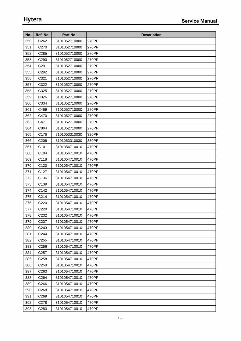
Service Manual
130
No. Ref. No. Part No. Description350 C262 3101052710000 270PF
351 C270 3101052710000 270PF
352 C285 3101052710000 270PF
353 C290 3101052710000 270PF
354 C291 3101052710000 270PF
355 C292 3101052710000 270PF
356 C321 3101052710000 270PF
357 C322 3101052710000 270PF
358 C325 3101052710000 270PF
359 C326 3101052710000 270PF
360 C334 3101052710000 270PF
361 C469 3101052710000 270PF
362 C470 3101052710000 270PF
363 C471 3101052710000 270PF
364 C804 3101052710000 270PF
365 C176 3101053310030 330PF
366 C208 3101053310030 330PF
367 C101 3101054710010 470PF
368 C104 3101054710010 470PF
369 C118 3101054710010 470PF
370 C120 3101054710010 470PF
371 C127 3101054710010 470PF
372 C136 3101054710010 470PF
373 C139 3101054710010 470PF
374 C142 3101054710010 470PF
375 C214 3101054710010 470PF
376 C220 3101054710010 470PF
377 C228 3101054710010 470PF
378 C232 3101054710010 470PF
379 C237 3101054710010 470PF
380 C243 3101054710010 470PF
381 C244 3101054710010 470PF
382 C255 3101054710010 470PF
383 C256 3101054710010 470PF
384 C257 3101054710010 470PF
385 C258 3101054710010 470PF
386 C259 3101054710010 470PF
387 C263 3101054710010 470PF
388 C264 3101054710010 470PF
389 C266 3101054710010 470PF
390 C268 3101054710010 470PF
391 C269 3101054710010 470PF
392 C278 3101054710010 470PF
393 C280 3101054710010 470PF

Service Manual
131
No. Ref. No. Part No. Description394 C281 3101054710010 470PF
395 C282 3101054710010 470PF
396 C283 3101054710010 470PF
397 C284 3101054710010 470PF
398 C287 3101054710010 470PF
399 C288 3101054710010 470PF
400 C293 3101054710010 470PF
401 C294 3101054710010 470PF
402 C295 3101054710010 470PF
403 C296 3101054710010 470PF
404 C297 3101054710010 470PF
405 C298 3101054710010 470PF
406 C299 3101054710010 470PF
407 C300 3101054710010 470PF
408 C301 3101054710010 470PF
409 C302 3101054710010 470PF
410 C303 3101054710010 470PF
411 C305 3101054710010 470PF
412 C313 3101054710010 470PF
413 C315 3101054710010 470PF
414 C316 3101054710010 470PF
415 C317 3101054710010 470PF
416 C320 3101054710010 470PF
417 C331 3101054710010 470PF
418 C332 3101054710010 470PF
419 C333 3101054710010 470PF
420 C335 3101054710010 470PF
421 C336 3101054710010 470PF
422 C444 3101054710010 470PF
423 C459 3101054710010 470PF
424 C512 3101054710010 470PF
425 C652 3101054710010 470PF
426 C663 3101054710010 470PF
427 C680 3101054710010 470PF
428 C681 3101054710010 470PF
429 C685 3101054710010 470PF
430 C703 3101054710010 470PF
431 C704 3101054710010 470PF
432 C835 3101054710010 470PF
433 C838 3101054710010 470PF
434 C842 3101054710010 470PF
435 C845 3101054710010 470PF
436 C846 3101054710010 470PF
437 C848 3101054710010 470PF

Service Manual
132
No. Ref. No. Part No. Description438 C849 3101054710010 470PF
439 C851 3101054710010 470PF
440 C853 3101054710010 470PF
441 C856 3101054710010 470PF
442 C857 3101054710010 470PF
443 C9018 3101054710010 470PF
444 C9029 3101054710010 470PF
445 C9033 3101054710010 470PF
446 C9034 3101054710010 470PF
447 C9037 3101054710010 470PF
448 C9039 3101054710010 470PF
449 C9042 3101054710010 470PF
450 C9045 3101054710010 470PF
451 C9047 3101054710010 470PF
452 C9048 3101054710010 470PF
453 C9069 3101054710010 470PF
454 C9075 3101054710010 470PF
455 C9081 3101054710010 470PF
456 C9096 3101054710010 470PF
457 C9098 3101054710010 470PF
458 C324 3101064710000 470PF
459 C9013 3101064710000 470PF
460 C260 3101055610000 560PF
461 C261 3101055610000 560PF
462 C9067 3101055610000 560PF
463 C137 3101051020010 1000PF
464 C156 3101051020010 1000PF
465 C161 3101051020010 1000PF
466 C162 3101051020010 1000PF
467 C163 3101051020010 1000PF
468 C172 3101051020010 1000PF
469 C180 3101051020010 1000PF
470 C183 3101051020010 1000PF
471 C184 3101051020010 1000PF
472 C202 3101051020010 1000PF
473 C206 3101051020010 1000PF
474 C211 3101051020010 1000PF
475 C705 3101051020010 1000PF
476 C9001 3101051020010 1000PF
477 C9036 3101051020010 1000PF
478 C9059 3101051020010 1000PF
479 C9061 3101051020010 1000PF
480 C9064 3101051020010 1000PF
481 C9085 3101051020010 1000PF

Service Manual
133
No. Ref. No. Part No. Description482 C9088 3101051020010 1000PF
483 C9089 3101051020010 1000PF
484 C9093 3101051020010 1000PF
485 C9103 3101051020010 1000PF
486 C9121 3101051020010 1000PF
487 C9123 3101051020010 1000PF
488 C9060 3101061020000 1000PF
489 L9039 3101061020000 1000PF
490 C275 3101051520000 1500PF
491 C276 3101051520000 1500PF
492 C277 3101051520000 1500PF
493 C289 3101051520000 1500PF
494 C304 3101051520000 1500PF
495 C9065 3101051520000 1500PF
496 C455 3101063320000 3300PF
497 C209 3101053920000 3900PF
498 C217 3101053920000 3900PF
499 C219 3101053920000 3900PF
500 C227 3101053920000 3900PF
501 C231 3101053920000 3900PF
502 C233 3101053920000 3900PF
503 C239 3101053920000 3900PF
504 C240 3101053920000 3900PF
505 C241 3101053920000 3900PF
506 C245 3101053920000 3900PF
507 C246 3101053920000 3900PF
508 C247 3101053920000 3900PF
509 C638 3101053920000 3900PF
510 C650 3101053920000 3900PF
511 C662 3101053920000 3900PF
512 C666 3101053920000 3900PF
513 C684 3101053920000 3900PF
514 C686 3101053920000 3900PF
515 C687 3101053920000 3900PF
516 C808 3101053920000 3900PF
517 C813 3101053920000 3900PF
518 C820 3101053920000 3900PF
519 C823 3101053920000 3900PF
520 C858 3101053920000 3900PF
521 C9063 3101054720000 4700PF
522 C437 3101065620010 5600PF
523 C174 3101051030020 0.01UF
524 C215 3101051030020 0.01UF
525 C251 3101051030020 0.01UF

Service Manual
134
No. Ref. No. Part No. Description526 C426 3101051030020 0.01UF
527 C436 3101051030020 0.01UF
528 C440 3101051030020 0.01UF
529 C447 3101051030020 0.01UF
530 C449 3101051030020 0.01UF
531 C453 3101051030020 0.01UF
532 C454 3101051030020 0.01UF
533 C457 3101051030020 0.01UF
534 C647 3101051030020 0.01UF
535 C651 3101051030020 0.01UF
536 C668 3101051030020 0.01UF
537 C819 3101051030020 0.01UF
538 C822 3101051030020 0.01UF
539 C826 3101051030020 0.01UF
540 C827 3101051030020 0.01UF
541 C837 3101051030020 0.01UF
542 C9044 3101051030020 0.01UF
543 C9066 3101051030020 0.01UF
544 C9087 3101051030020 0.01UF
545 C9090 3101051030020 0.01UF
546 C9110 3101051030020 0.01UF
547 C9138 3101051030020 0.01UF
548 C442 3101061030010 0.01UF
549 C619 3101061030010 0.01UF
550 C450 3101061230000 0.012UF
551 C105 3101051040060 0.1UF
552 C117 3101051040060 0.1UF
553 C121 3101051040060 0.1UF
554 C126 3101051040060 0.1UF
555 C138 3101051040060 0.1UF
556 C141 3101051040060 0.1UF
557 C164 3101051040060 0.1UF
558 C165 3101051040060 0.1UF
559 C166 3101051040060 0.1UF
560 C167 3101051040060 0.1UF
561 C169 3101051040060 0.1UF
562 C179 3101051040060 0.1UF
563 C182 3101051040060 0.1UF
564 C310 3101051040060 0.1UF
565 C311 3101051040060 0.1UF
566 C318 3101051040060 0.1UF
567 C422 3101051040060 0.1UF
568 C430 3101051040060 0.1UF
569 C433 3101051040060 0.1UF

Service Manual
135
No. Ref. No. Part No. Description570 C434 3101051040060 0.1UF
571 C435 3101051040060 0.1UF
572 C441 3101051040060 0.1UF
573 C445 3101051040060 0.1UF
574 C446 3101051040060 0.1UF
575 C462 3101051040060 0.1UF
576 C464 3101051040060 0.1UF
577 C465 3101051040060 0.1UF
578 C466 3101051040060 0.1UF
579 C522 3101051040060 0.1UF
580 C523 3101051040060 0.1UF
581 C525 3101051040060 0.1UF
582 C604 3101051040060 0.1UF
583 C607 3101051040060 0.1UF
584 C615 3101051040060 0.1UF
585 C617 3101051040060 0.1UF
586 C618 3101051040060 0.1UF
587 C622 3101051040060 0.1UF
588 C625 3101051040060 0.1UF
589 C626 3101051040060 0.1UF
590 C630 3101051040060 0.1UF
591 C635 3101051040060 0.1UF
592 C639 3101051040060 0.1UF
593 C642 3101051040060 0.1UF
594 C656 3101051040060 0.1UF
595 C658 3101051040060 0.1UF
596 C659 3101051040060 0.1UF
597 C671 3101051040060 0.1UF
598 C679 3101051040060 0.1UF
599 C682 3101051040060 0.1UF
600 C688 3101051040060 0.1UF
601 C710 3101051040060 0.1UF
602 C801 3101051040060 0.1UF
603 C809 3101051040060 0.1UF
604 C810 3101051040060 0.1UF
605 C812 3101051040060 0.1UF
606 C833 3101051040060 0.1UF
607 C836 3101051040060 0.1UF
608 C839 3101051040060 0.1UF
609 C843 3101051040060 0.1UF
610 C850 3101051040060 0.1UF
611 C852 3101051040060 0.1UF
612 C9038 3101051040060 0.1UF
613 C9041 3101051040060 0.1UF

Service Manual
136
No. Ref. No. Part No. Description614 C9043 3101051040060 0.1UF
615 C9046 3101051040060 0.1UF
616 C9049 3101051040060 0.1UF
617 C9057 3101051040060 0.1UF
618 C9071 3101051040060 0.1UF
619 C9080 3101051040060 0.1UF
620 C9086 3101051040060 0.1UF
621 C9091 3101051040060 0.1UF
622 C9092 3101051040060 0.1UF
623 C9097 3101051040060 0.1UF
624 C9104 3101051040060 0.1UF
625 C212 3101052240010 0.22UF
626 C213 3101052240010 0.22UF
627 C216 3101052240010 0.22UF
628 C218 3101052240010 0.22UF
629 C221 3101052240010 0.22UF
630 C222 3101052240010 0.22UF
631 C226 3101052240010 0.22UF
632 C230 3101052240010 0.22UF
633 C234 3101052240010 0.22UF
634 C238 3101052240010 0.22UF
635 C242 3101052240010 0.22UF
636 C248 3101052240010 0.22UF
637 C249 3101052240010 0.22UF
638 C683 3101052240010 0.22UF
639 C803 3101052240010 0.22UF
640 C821 3101052240010 0.22UF
641 C824 3101052240010 0.22UF
642 C210 3101062240000 0.22UF
643 C628 3101062240000 0.22UF
644 C640 3101062240000 0.22UF
645 C655 3101062240000 0.22UF
646 C676 3101062240000 0.22UF
647 C678 3101062240000 0.22UF
648 C463 3101072240000 0.22UF
649 C177 3101074740000 0.47UF
650 C468 3104076840020 0.68UF
651 C236 3101051050000 1UF
652 C312 3101051050000 1UF
653 C314 3101051050000 1UF
654 C323 3101051050000 1UF
655 C423 3101051050000 1UF
656 C515 3101051050000 1UF
657 C526 3101051050000 1UF

Service Manual
137
No. Ref. No. Part No. Description658 C706 3101051050000 1UF
659 C707 3101051050000 1UF
660 C711 3101051050000 1UF
661 C712 3101051050000 1UF
662 C831 3101051050000 1UF
663 C832 3101051050000 1UF
664 C834 3101051050000 1UF
665 C840 3101051050000 1UF
666 C847 3101051050000 1UF
667 C9052 3101051050000 1UF
668 C9095 3101051050000 1UF
669 C605 3101061050020 1UF
670 C623 3101061050020 1UF
671 C648 3101061050020 1UF
672 C669 3101061050020 1UF
673 C677 3101061050020 1UF
674 C701 3101061050020 1UF
675 C816 3101061050020 1UF
676 C140 3101062250000 2.2UF
677 C157 3101062250000 2.2UF
678 C158 3101062250000 2.2UF
679 C467 3101062250000 2.2UF
680 C472 3101062250000 2.2UF
681 C601 3101062250000 2.2UF
682 C606 3101062250000 2.2UF
683 C624 3101062250000 2.2UF
684 C641 3101062250000 2.2UF
685 C649 3101062250000 2.2UF
686 C653 3101062250000 2.2UF
687 C660 3101062250000 2.2UF
688 C670 3101062250000 2.2UF
689 C825 3101062250000 2.2UF
690 C828 3101062250000 2.2UF
691 C185 3104072250060 2.2UF
692 C621 3101074750000 4.7UF
693 C629 3101074750000 4.7UF
694 C636 3110071060000 10uF
695 C661 3110071060000 10uF
696 C627 3110081060000 10uF
697 C654 3110081060000 10uF
698 C9051 3104082260060 22UF
699 C637 3110994760000 47uF
700 C665 3110994760000 47uF
701 L407 3221505121010 Bead

Service Manual
138
No. Ref. No. Part No. Description702 L801 3221505121010 Bead
703 L803 3221505121010 Bead
704 L804 3221505121010 Bead
705 L805 3221505121010 Bead
706 L821 3221505121010 Bead
707 L822 3221505121010 Bead
708 L9015 3221505121010 Bead
709 L9020 3221505121010 Bead
710 L302 3221506601000 Bead
711 L304 3221506601000 Bead
712 L305 3221506601000 Bead
713 L410 3221506601000 Bead
714 L823 3221506601000 Bead
715 L827 3221506601000 Bead
716 L828 3221506601000 Bead
717 L502 3221506601080 Bead
718 L505 3221506601080 Bead
719 L303 3221506181000 Bead
720 L601 3221506181000 Bead
721 L602 3221506181000 Bead
722 L603 3221506181000 Bead
723 L605 3221506181000 Bead
724 L606 3221506181000 Bead
725 L609 3221506181000 Bead
726 L611 3221506181000 Bead
727 L612 3221506181000 Bead
728 L617 3221506181000 Bead
729 L802 3221506181000 Bead
730 R614 3221506181000 Bead
731 R622 3221506181000 Bead
732 L9014 3221506121000 Bead
733 L9040 3217105010000 1nH
734 L9030 3210306279000 2.7nH
735 L501 3297106339000 3.3nH
736 L503 3297106339000 3.3nH
737 L504 3297106339000 3.3nH
738 L9016 3210306339000 3.3nH
739 L508 3210305829000 8.2nH
740 L509 3210305829000 8.2nH
741 L9006 3212106829000 8.2nH
742 L9007 3212106829000 8.2nH
743 L104 3210106100010 10nH
744 L105 3210106100010 10nH
745 L102 3212106100000 10nH

Service Manual
139
No. Ref. No. Part No. Description746 L103 3212106100000 10nH
747 L9018 3210106150000 15nH
748 L9033 3237199170000 17nH
749 L9035 3237199170000 17nH
750 L9036 3237199170000 17nH
751 L9037 3237199170000 17nH
752 L507 3210305180000 18nH
753 L117 3217107120000 12nH
754 L112 3217107160000 16nH
755 L9017 3217106180010 18nH
756 L9028 3210106220000 22nH
757 L9009 3210306150000 15nH
758 L9010 3210306150000 15nH
759 L9003 3233099185900 18.5nH
760 L9004 3233099185900 18.5nH
761 L9005 3233099185900 18.5nH
762 L9013 3233099185900 18.5nH
763 L506 3210106390000 39nH
764 L9008 3233099470000 47nH
765 L9001 3210106820000 82nH
766 L9026 3210106101000 100nH
767 L9012 3210107221000 220nH
768 L9024 3217107331000 330nH
769 L402 3210406271000 270nH
770 L9022 3210406271000 270nH
771 L106 3210106391000 390nH
772 L108 3210106391000 390nH
773 L113 3210106391000 390nH
774 L114 3210106391000 390nH
775 L115 3210106391000 390nH
776 L116 3210106391000 390nH
777 L119 3210106391000 390nH
778 L124 3210406471000 470nH
779 L201 3210406471000 470nH
780 L409 3210406471000 470nH
781 L9027 3213306821000 0.82uH
782 L9011 3210209102010 1uH
783 L607 3290299222000 2.2uH
784 L613 3290299222000 2.2uH
785 L615 3290299222000 2.2uH
786 L616 3290299222000 2.2uH
787 L408 3210407472000 4.7uH
788 L413 3213306682000 6.8uH
789 L401 3215099103000 10uH

Service Manual
140
No. Ref. No. Part No. Description790 L404 3215099103000 10uH
791 L610 3217099153000 15uH
792 L614 3217099153000 15uH
793 D302 3303990000010 Switching diode
794 D601 3399990000110 Diode
795 D9002 3303030800040 Switching diode
796 D111 3304010100890 Varactor
797 D101 3304010100220 Varactor
798 D102 3304010100220 Varactor
799 D103 3304010100220 Varactor
800 D106 3304010100220 Varactor
801 D107 3304010100220 Varactor
802 D108 3304010100220 Varactor
803 D109 3304010100220 Varactor
804 D110 3304010100220 Varactor
805 D402 3304010100220 Varactor
806 D401 3304060300050 Varactor
807 D104 3303990000060 Switching diode
808 D105 3303990000060 Switching diode
809 D112 3303990000060 Switching diode
810 D9005 3303990000060 Switching diode
811 D9006 3303990000060 Switching diode
812 D9007 3303990000060 Switching diode
813 D604 3303030100010 Switching diode
814 D9011 3303030100010 Switching diode
815 D9010 3399990000080 Zener diode
816 D9013 3399990000260 Rectifier diode
817 D9017 3301250300000 Schottky barrier diode
818 D307 3399040600020 ESD protection diode
819 D308 3399040600020 ESD protection diode
820 D309 3399040600020 ESD protection diode
821 D310 3399040600020 ESD protection diode
822 D602 3399040600020 ESD protection diode
823 D318 3399040600010 ESD protection diode
824 D303 3399040600000 ESD protection diode
825 D304 3399040600000 ESD protection diode
826 D305 3399040600000 ESD protection diode
827 D306 3399040600000 ESD protection diode
828 Q9006 3410001000020 PNP transistor
829 Q102 3408002000000 NPN transistor
830 Q403 3408002000000 NPN transistor
831 Q9002 3408002000000 NPN transistor
832 Q105 3403003000060 NPN transistor
833 Q401 3403003000060 NPN transistor

Service Manual
141
No. Ref. No. Part No. Description834 Q9004 3406001000090 NPN transistor
835 Q101 3401002000990 NPN transistor
836 Q604 3503020000030 N-MOSFET
837 Q607 3503020000030 N-MOSFET
838 Q608 3503020000030 N-MOSFET
839 Q9001 3418001000010 NPN transistor
840 Q310 3511990000010 N-MOSFET
841 Q313 3511990000010 N-MOSFET
842 Q312 3403008000010 BRT
843 Q801 3403008000010 BRT
844 Q802 3403008000010 BRT
845 Q9007 3403008000010 BRT
846 Q9008 3403008000010 BRT
847 Q103 3403999000000 Compound transistor
848 Q106 3403999000000 Compound transistor
849 Q107 3403999000000 Compound transistor
850 Q9019 3403999000000 Compound transistor
851 Q9020 3403999000000 Compound transistor
852 Q603 3414001000040 NPN transistor
853 Q104 3408002000080 NPN transistor
854 Q108 3408002000080 NPN transistor
855 Q9017 3404006000000 NPN transistor
856 Q9018 3404006000000 NPN transistor
857 Q9005 3504990000010 MOSFET
858 Q9003 3504990000040 MOSFET
859 Q605 3505010000210 P-MOSFET
860 Q606 3505010000210 P-MOSFET
861 Q402 3499000000150 Compound transistor
862 U401 3603999000000 IF processor
863 U312 3805000000030 EMI filter
864 U313 3805000000030 EMI filter
865 U314 3805000000030 EMI filter
866 U315 3805000000030 EMI filter
867 U316 3805000000030 EMI filter
868 U317 3805000000030 EMI filter
869 U318 3805000000030 EMI filter
870 U319 3805000000030 EMI filter
871 U320 3805000000030 EMI filter
872 U321 3805000000030 EMI filter
873 U322 3805000000030 EMI filter
874 U101 3616059000000 Switch
875 U104 3616059000000 Switch
876 U9003 5404000000060 Sensor
877 U601 3608011000050 DC-DC

Service Manual
142
No. Ref. No. Part No. Description878 U611 3608011000050 DC-DC
879 U242 3612044000010 Memory
880 U9002 3605025000020 Operational amplifier
881 U820 3616037000020 Switch
882 U201 3610010000010 MCU
883 U610 3608006000030 Power management IC
884 U606 3608006000000 Power management IC
885 U608 3608006000000 Power management IC
886 U609 3608006000000 Power management IC
887 U612 3608006000000 Power management IC
888 U103 3604019000000 PLL
889 U102 3605002057290 Operational amplifier
890 U801 3602023005740 Audio amplifier
891 U604 3608020005750 Power management IC
892 U605 3608020005750 Power management IC
893 U821 3613010000000 Baseband processor
894 U701 3606010000010 D/A converter
895 U607 3609010000170 Reset IC
896 U244 3612002000020 Memory
897 U501 3609999000300 GPS LNA
898 ANT1 6201847000000 Antenna spring plate
899 F601 4099000000050 Fuse
900 F602 4010000000010 Fuse
901 J821 5201016000010 Board-to-board connector
902 J311 5201030000040 Board-to-board connector
903 J1601 5201050100030 Board-to-board connector
904 J313 5202002100200 Board-to-wire connector
905 J601 5205003100020 Battery connector
906 T9001 5406000000200 Transformer
907 T9002 5406000000200 Transformer
908 X101 3701019250030 TCXO
909 X203 3701019250040 TCXO
910 X201 3701327610060 Crystal
911 Z501 3804157560000 GPS filter
912 R404 3001051220000 1.2KΩ
913 L110 3210306221000 220nH
914 L9032 3210306221000 220nH
915 L9038 3210406331000 330nH
916 R9004 3233099449000 4.4nH
917 C802 3101071060010 10UF
918 C9011 3101061010010 100PF
919 Z9001 3802733540030 Crystal filter
920 U502 1615000001720 GPS module
921 R9020 3001051030010 10KΩ

Service Manual
143
No. Ref. No. Part No. Description922 R9023 3001053920010 3.9KΩ
923 R9047 3001053920010 3.9KΩ
924 C159 3101052220010 2200pF
925 C160 3101052220010 2200pF
926 C431 3101052220010 2200pF
927 C102 3101054790010 4.7PF
928 C103 3101054790010 4.7PF
929 C111 3101054790010 4.7PF
930 C112 3101054790010 4.7PF
931 C130 3101062700010 27PF
932 C9007 3101060700020 7PF
933 C152 3101060500010 5PF
934 C452 3101060500010 5PF
935 C9015 3101060500010 5PF
936 Q9021 3401001000490 PNP transistor
937 C178 3101074740000 0.47UF
938 C9003 3199060758000 0.75PF
939 L101 3210306220000 22nH
940 L107 3210306270000 27nH
941 L9002 3210306560000 56nH
942 L9025 3210306560000 56nH
943 L406 3217107221020 220nH
944 D9001 3304010100200 Varactor
945 D9012 3304010100200 Varactor
946 D9014 3304010100200 Varactor
947 D9015 3304010100200 Varactor
948 D9016 3304010100200 Varactor
949 L109 3221505121000 Bead
950 L120 3221505121000 Bead
951 L121 3221505121000 Bead
952 L122 3221505121000 Bead
953 L123 3221505121000 Bead
954 L125 3221505121000 Bead
955 L403 3221505121000 Bead
956 L405 3221505121000 Bead
957 L412 3221505121000 Bead
958 L702 3221505121000 Bead
959 R712 3221505121000 Bead
960 L118 3237138689000 6.8nH
961 C9134 3101057590000 7.5PF
962 L411 3217107392000 3.9uH
963 D9008 3303060300010 Switching diode
964 L111 3247107180000 18nH
965 R124 3001051220090 1.2KΩ

Service Manual
144
No. Ref. No. Part No. Description966 R125 3001051220090 1.2KΩ
967 R9056 3001051240010 120KΩ
968 R123 3001051840010 180KΩ
969 C154 3001052220010 2.2KΩ
970 R122 3001053320010 3.3KΩ
971 R120 3001054790010 4.7KΩ
972 R601 3001059130000 91KΩ
973 C608 3101051050160 1uF
974 C9111 3101050690050 6PF
975 C149 3101060200010 2PF
976 C458 3101061800000 18PF
977 6201810000000 Shielding can for baseband processor
978 6201860000000 Shielding frame for GPS
979 6201865000000 Shielding can for crystal oscillator
980 6201915000000 Shielding can for antenna spring plate
981 6201935000000 Shielding can for switching power
982 6201859000000 Shielding frame for lowpass filter
983 6201862000000 Shielding can for TX VCO984 41PD7001000K0 Main board
985 9830000000001 Voice coding software

Service Manual
145
Channel Board for PD70X/ PD70XG/ HD705/ HD705G No. Ref. No. Part No. Description1 R1002 3001051210010 120Ω
2 C1001 3101052710000 270PF
3 C1002 3101052710000 270PF
4 C1003 3101052710000 270PF
5 C1004 3101052710000 270PF
6 C1005 3101052710000 270PF
7 C1006 3101052710000 270PF
8 C1007 3101052710000 270PF
9 C1010 3101052710000 270PF
10 C1011 3101052710000 270PF
11 C1012 3101052710000 270PF
12 D1001 3310040000000 ESD protection diode
13 D1003 3310040000000 ESD protection diode
14 D1004 3310040000000 ESD protection diode
15 D1005 3310040000000 ESD protection diode
16 D1006 3310040000000 ESD protection diode
17 D1007 3310040000000 ESD protection diode
18 D1008 3310040000000 ESD protection diode
19 D1011 3310040000000 ESD protection diode
20 D1014 3310040000000 ESD protection diode
21 D1009 3399040600020 ESD protection diode
22 D1013 3399040600020 ESD protection diode
23 D1002 3307120100050 LED
24 Q1001 3403009000010 Compound transistor
25 U1001 3805000000040 EMI filter
26 J1001 5201016100040 Board-to-board connector
27 S1003 4301080000020 Momentary contact switch
28 41PD7002002B0 PCB
29 R1001 3001056810000 680Ω
30 C1015 3101051040060 0.1UF
31 C1016 3101051040060 0.1UF
32 C1017 3101051040060 0.1UF
33 L1001 3221506181000 Bead
34 U1002 3608006000030 Power management IC

Service Manual
146
Channel Board for PD78X/ PD78XG/ HD785/ HD785G No. Ref. No. Part No. Description1 R1002 3001051210010 120Ω
2 C1001 3101052710000 270PF
3 C1002 3101052710000 270PF
4 C1003 3101052710000 270PF
5 C1004 3101052710000 270PF
6 C1005 3101052710000 270PF
7 C1006 3101052710000 270PF
8 C1007 3101052710000 270PF
9 C1010 3101052710000 270PF
10 C1011 3101052710000 270PF
11 C1012 3101052710000 270PF
12 D1001 3310040000000 ESD protection diode
13 D1003 3310040000000 ESD protection diode
14 D1004 3310040000000 ESD protection diode
15 D1005 3310040000000 ESD protection diode
16 D1006 3310040000000 ESD protection diode
17 D1007 3310040000000 ESD protection diode
18 D1008 3310040000000 ESD protection diode
19 D1011 3310040000000 ESD protection diode
20 D1014 3310040000000 ESD protection diode
21 D1009 3399040600020 ESD protection diode
22 D1013 3399040600020 ESD protection diode
23 D1002 3307120100050 LED
24 Q1001 3403009000010 Compound transistor
25 U1001 3805000000040 EMI filter
26 J1001 5201016100040 Board-to-board connector
27 S1003 4301080000020 Momentary contact switch
28 41PD7802006C0 PCB
29 R1001 3001056810000 680Ω
30 C1015 3101051040060 0.1UF
31 C1016 3101051040060 0.1UF
32 C1017 3101051040060 0.1UF
33 L1001 3221506181000 Bead
34 U1002 3608006000030 Power management IC

Service Manual
147
Keyboard for PD78X/ PD78XG/ HD785/ HD785G
No. Ref. No. Part No. Description1 R1 3001051010000 100Ω
2 R2 3001051010000 100Ω
3 R3 3001051010000 100Ω
4 R4 3001051010000 100Ω
5 R5 3001051010000 100Ω
6 R6 3001051010000 100Ω
7 R7 3001051010000 100Ω
8 D1 3307990000260 LED
9 D2 3307990000260 LED
10 D3 3307990000260 LED
11 D4 3307990000260 LED
12 D5 3307990000260 LED
13 D6 3307990000260 LED
14 D7 3307990000260 LED
15 D8 3310040000010 ESD protection diode
16 D9 3310040000010 ESD protection diode
17 J4 5201016000010 Board-to-board connector

Service Manual
148
11.8 Troubleshooting Flow Chart Receiver Circuit

Service Manual
149
Description of Normal Situations: [1] Output voltage by Q9019 PIN3: about 4.95V. [2] Output voltage by U605 PIN4 or input voltage into Q9019 PIN4: about 5V. [3] Vbe: about 0.74V; Vce: about 2.5V (in the case of no signal reception). [4] For Q9018, Vbe: about 0.76V; Vce: about 0.95V; for Q9017, Vbe: about 0.7V; Vce:0.85V (in the case of no signal reception). [5] Cut off the front-end circuit, and input a 73.35MHz IF signal at TP402 to test IF sensitivity. Normally, the IF sensitivity is -109dBm. [6] Frequency of Q403: 71.1MHz. [7] Frequency of L411: 18MHz. [8] Input -30dBm RF signal at the antenna connector and test at TP9004. Normally, gain>10dB, output signal>-20dBm. [9] Input -30dBm RF signal at the antenna connector and test at R9005 (do not cut off the back-end circuit). Normally, gain>1dB, output signal>-29dBm. [10] Signal frequency: RF-IF, signal amplitude>2dBm. [11] For input of -80dBm signal at L9022, gain>25dB, output signal>-55dBm; for input of -30dBm signal, output signal<-20dBm. [12] The input signal at the antenna connector, with standard tuning information (AF=1KHz, FM=3KHz), is -47dBm.

Service Manual
150
Transmitter Circuit
No power output
Power supply works normally?[1]
Check the power supply circuit.
No
APC-OUT is normal?[2]
TX 5V voltageis normal?[5]
APC-IN is normal?[3]
Yes
No
PS-APC 3.3V is normal?[4]
Yes
PS-TX and RT5V are normal?[5]
No
Yes
No
Match circuit is normal?[8]
Yes
Yes
No
Q9003 works normally?[9]
Yes
Repair damaged components.
Power is normal? CompletedYesNo
No Replace Q9003 and bias resistor.
Power is normal? CompletedYes
Q9005 works normally?[10]
D9002,spring plate for antenna and the low-pass
filter are normal?[7]
Repair damaged components.
Yes
No
Power is normal? CompletedYesNo
NoYes
Replace Q9005 and bias resistor.
Q9004 works normally?[11]
Power is normal? CompletedYesNoYes
No
Replace Q9004 and bias resistor.
Power is normal? CompletedYesNo
No
Q9002/D9007 works normally?[12]
Replace Q9002 and bias resistor.
Power is normal? CompletedYesNo
Check the output circuit of FGU.
No
Yes
Replace Q9020 and U9002.
Power is normal?[6] Completed
YesNo
Yes
Check the DAC output circuit.
Yes Replace Q9008 and Q9006.
Check the power supply circuit.
No
No

Service Manual
151
Description of Normal Situations: [1] Voltage of the power supply: about 7.4V. [2] For low power, APC-OUT: 1.8-2.1V; for high power, APC-OUT: 2.4-2.8V. [3] For low power, APC-IN: 1-1.3V; for high power, APC-IN: 1.8-2.1V. [4] PS-APC: about 3.3V. [5] TX5V: about 5V; RT5V: about 5V; PS-TX: about 3.3V. [6] High power: about 4.2W; low power: about 1.2W. [7] Start-up voltage of D9002: about 0.7V. The low-pass filter must be soldered appropriately and remain in good condition. The spring plate for the antenna must be well fitted into the antenna connector. [8] The match components must not be soldered inappropriately or damaged. [9] Vdd: about 7.3V; for low power, Vgg: 1-1.2V; for high power, Vgg: 1.35-1.55V. [10] Vdd: about 7.3V; for low power, Vgg: 1.7-2.1V; for high power, Vgg: 2.4-2.8V. [11] Vc: about 4.8V; Vb: about 1.4V; Ve: about 1.1V. [12] Vc: about 4.7V; Vb: about 0.7V; Ve: 0V. Start-up voltage of D9007: about 0.7V. Note: The above check operations should be made under 7.4V voltage.

Service Manual
152
FGU
FGU check
Check the power supply circuit.5VFGU, 3V3ARF,
3V3DRF are normal?
VCO oscillates?
Q106 、Q110输出是否正常?
反馈是
否正常?
Yes
Yes
Yes
CV voltage is normal?[3]
Feedback is output?
Yes
Yes
Yes
No
Replace Q106 and Q107.
Q106 and Q107 are normal?[1]
Q104 and Q108 are normal?[2]
No
No
YesReplace Q104
and Q108.
No
Check Q104, Q108 and peripheral components.
Yes
NoL110 and L116 are
normal?[4]Replace L110 and
L116.
No
Q101 and Q102 are normal?[5]
Check the feedback circuit.
No
19.2MHz crystal oscillates?
Check the 19.2MHz circuit.
No
Sky72310 clock is normal?[6]
CompletedYes
Check the data circuit of the
control circuit.
No
Check Q101, Q102 and peripheral components.
Replace Q101 and Q102.
No
Yes

Service Manual
153
Description of Normal Situations: [1] During transmission, output voltage by Q107 PIN3: about 4V. During reception, output voltage by Q106 PIN3: about 4V. [2] During transmission, voltage at Q108 E: about 1.8V. During reception, voltage at Q104 E: about 1.8V. [3] The CV value varies with frequencies. Generally, it is within the range 0.5V-4.5V. [4] L110/L116 is on. [5] Voltage at Q101/Q102 B: about 0.7V. [6] MCSI-CLK-PLL outputs 960KHz clock.

Service Manual
154
12. UHF3 (350-400MHz) Information
12.1 Transmitter Circuit
Figure 12-1 Diagram of Transmitter Circuit
The transmitter circuit is mainly composed of:
① RF power amplifier circuit
② Low-pass filter circuit (for suppressing harmonics)
③ Auto power control circuit (APC) (including temperature detection circuit)
The carrier signal generated by TX VCO is modulated and amplified, and then feeds to the transmitter
circuit. In this circuit, the signal passes through a π-type attenuator first, allowing certain isolation
between the RF power amplifier circuit and TX VCO. Then it goes to a pre-driver amplifier (2SC3356) for
pre-amplification, also providing certain isolation. After that, the signal goes to another pre-driver
amplifier (2SC4988) and a driver amplifier (RD01) for further power amplification, to provide appropriate
signal to the final-stage amplifier (RD07) for final power amplification. After processed by multiple
amplifiers, the signal is processed by a microstrip matcher to complete output impedance matching, so
as to reduce output power loss due to impedance mismatch. Then the signal passes through the TX/RX
switch and goes to the low-pass filter.
The low-pass filter is a high-order Chebyshev filter composed of lumped-parameter inductors and
capacitors. Via this filter, the spurious signal within the stop band can be attenuated as much as possible
while the in-band ripple is within the required range.

Service Manual
155
In the auto power control and temperature detection circuit, the drain current from the driver amplifier
and final-stage amplifier is converted to voltage via the sampling resistor and subtraction circuit
(composed of the first operational amplifier). This voltage is compared with the APC control voltage
(output by DAC) at the second operational amplifier. Then the error voltage, which is output by the
second operational amplifier, controls TX power by controlling the bias voltage at the gates of the
amplifiers (including the driver amplifier and the final-stage amplifier). The temperature sensor detects
the surface temperature of the final-stage amplifier, and converts it to DC voltage. Then the DC voltage is
compared with the voltage corresponding to the protection temperature (generally 80% of the extreme
temperature) of the amplifier. If the surface temperature is too high, the bias voltage of the amplifier will
be reduced, so as to reduce output power. The bias voltage will not be increased until the surface
temperature restores to normal level. This process will be repeated while the radio operates.
12.2 Receiver Circuit
Pi Attenuator
1 2
Figure 12-2 Diagram of Receiver Circuit
The receiver circuit mainly comprises the RF band-pass filter, low-noise amplifier, mixer, IF filter, IF
amplifier and IF processor.
12.2.1 Receiver Front-end
The HF signal from the low-pass filter passes through the electrically tunable band-pass filter controlled
via APC/TV1 level, to remove out-of-band interference signal and to send wanted band-pass signal to
the low-noise amplifier (Q9001). The amplified signal goes to a band-pass filter controlled via APC/TV1

Service Manual
156
level, to remove out-of-band interference signal generated during amplification, and to send wanted HF
signal to the mixer.
The wanted signal passes through the RF band-pass filter and low-noise amplifier and goes to the mixer
(D9017). Meanwhile, the first local oscillator (LO) signal generated by VCO passes through the low-pass
filter and also goes to the mixer (D9017). In the mixer, the wanted signal and the first LO signal are
mixed to generate the first IF signal (73.35MHz). Then the signal passes through a π-type attenuator
(2dB) and the LC, to suppress carrier other than the first IF signal, and to increase the isolation between
the mixer and the IF filter. After that, the first IF signal is processed by the crystal filter (Z9001), and is
sent to the two-stage IF amplifier circuit (composed of 2SC3356) for amplification. Then the amplified
signal goes to the IF processor AD9864(U401) for processing.
12.2.2 Receiver Back-end
Figure 12-3 Diagram of IF Processor
The first IF signal (73.35MHz) output by the IF amplifier goes into AD9864 (U401) via Pin 47, where the
signal is converted to the second IF signal (2.25MHz). Then the signal is converted to digital signal via
ADC sampling, and output via the SSI interface. Finally, the digital signal is sent to DSP (OMAP5912) for
demodulation.
AD9864 employs reference frequency of 19.2MHz and shares the crystal with OMAP. The second LO
VCO comprises an oscillator, a varactor and some other components, to provide the 71.1/75.6MHz LO
signal. The 18MHz clock frequency is generated by the LC resonance loop.

Service Manual
157
12.3 Frequency Generation Unit (FGU)
Figure 12-4 Diagram of FGU
The FGU is composed of VCO and PLL. It is the core module of the whole TX-RX system. This circuit
provides accurate carrier frequency during transmission, and stable LO signal during reception. It has a
direct influence on the performance of the system.
12.3.1 Working Principle of PLL
The 19.2MHz frequency generated by the reference crystal oscillator goes to PLL for division, generating
the reference frequency (i.e. step frequency f1). Meanwhile, the frequency generated by VCO generates
another frequency (f2) through the frequency divider in PLL. Then frequencies f1 and f2 are compared in
the phase detector (PD), to generate continuous pulse current. The current goes to the loop filter for RC
integration, and is then converted to CV voltage. Then the CV voltage is sent to the varactor of VCO. It
adjusts the output frequency of VCO directly until the CV voltage becomes constant. Then PLL is locked,
and the stable frequency output by VCO goes to the TX-RX channel after passing through two buffer
amplifiers.
12.3.2 Working Principle of VCO
VCO employs Colpitts oscillator circuit (the RX oscillator circuit is composed of D102, D103, D106, D107
and L112; the TX oscillator circuit is composed of D108, D109, D110, D101 and L117). It obtains different

Service Manual
158
output frequencies by changing the varactor's control voltage (i.e. CV voltage).
There are two types of VCO: TX VCO and RX VCO. Both types control EMD22 to switch operating
status via OMAP. RX VCO is composed of the oscillator loop and Q104, to provide LO signal. TX VCO is
composed of the oscillator loop and Q108, to provide carrier for TX signal.
12.3.3 Two-point Modulation
In TX mode, the two-point modulation technology is employed, to obtain higher modulation accuracy and
lower 4FSK bit error rate. MOD-VCO and MOD-XO send the modulation signal to the modulation end of
VCO and the reference crystal oscillator of PLL respectively to modulate TX VCO and the reference
crystal oscillator.


Pre-Drive2 Drive-stage Final-stage Tx/Rx Switch Low-pass Filter
Tx_VCO
AD9864
FrequencySynthesizer
Rx_VCO
Band-pass Filter1Low-Noise AmpBand-pass Filter2MixerIF FilterIF Processor IF Amp
Ref. Osc19.2MHZ
.
MOD1
MO
D2+
Freq
err
or s
hift
OMAP
4CH DAC
GPS module
BPF
HPF
ANTMicrostrip Matcher
TV1/APC
LPF
RX/TX VCO
amplifier
TO omap
TV1 /APC
From OMAP
TV1/APC
Reference OSC signal
CV Buffer
Pi Attenuator
1 2
BATT+
Stop band filter
Adapt SW
Adapt control
APC module
Low-Noise Amp
OP
Pre-driver1
RX/TX VCO buffer LPF
LPF
Pi Attenuator
1 2
CV SW
CV-read control
CV out
1
2
P i Attenuator
Pi Attenuator


LDO: 5V
LDO:5V
DC to DC 600mA
DC to DC 600mA
15mA/3V3D
RF PA 7.4V/1.6ARQA0002DNS
Vcc1 /2 2.2V-18V 210mA/Po=0.89W/7.4V
AF PA(TDA8547TS)
DVDD 1.65V-1.8V-1.95V Digital coreIOVDD 2V- 3.6V(MCLK=100M) I/O
2V- 3.6V(MCLK=50M)1.1V-2.5V External
VREF 2.3V-2.5V-2.7V Pro=2.5V SAR ADC reference voltage 1.25V Pro=1.25VVBAT 0.5V-6V Battery monitor input
Codec(TLV320AIC29IRGZR)AVDD1 3V-3.3V-3.6V Audio ADC,DAC,Reference,SAR ADCAVDD2 3V-3.3V-3.6V PLL analogBVDD 3V-4.2V Battery power supplyDRVDD 3V-3.3V-3.6V Headphone driver
Vcc (3.0V-5.5V)/1mA(No load max)
DVDD 4.5V-5V-5.5V(5V Supply) 2.7V-3V-3.3V(3 Supply)
DAC(TLV5604) No load,run clk:: Slow1.4mA/Fast 3.5mA(5V) Slow1mA/Fast 3mA(3V)AVDD 4.5V-5V-5.5V(5V Supply) 2.7V-3V-3.3V(3 Supply)Vref
VCCcp_main: Charge pump supply, 2.7V-5V(3 to 5 V);
VCCdigital: Digital supply, 2.7V-3V-3.3V;
VCCxtal : Crystal oscillator ECL/CML, 2.7V-3V-3.3V;VCCecl/cml: ECL/CML, 2.7V-3V-3.3V;
VDD 3.3V/15mA(EMIFS Bus is used 3V3D)
LCM(TFT)VLED (1*WLED 3.2±0.2V/15mA)
Vcc 2.7V-3.1V /33mA(read while write)
MCU(Nor FLASH+PsRAM))
VDD/Q 1.7V-1.8-1.95V /50mA Operation mode
SDRAM
DVDDI/O(1.71V-1.8V-AVDD)
AVDD(2.4V-2.8V-3.6V)
OMAP5912CVDDCVDD1CVDD2CVDD3CVDDRTC
Low power standby (1.05V-1.1V-1.21V)
Active mode(1.525V-1.6V-1.65V)
core logic and low voltage sections of I/Ocore logicMPU subsystem logic and memoryDSP subsystem logic and memoryRTC core logic
CVDDACVDDDLL
1.525V-1.6V-1.65V
1.525V-1.6V-1.65VAPLL provide 48MHz to peripherals(DDR)SDRAM timing
Peripheral I/O buffersMCSI2 and McBSP2 peripheral I/O buffersFlash I/F I/O buffersMMC/SD1 I/F I/O buffersMcBSP3,MCSI1,UART,USB1 I/O buffersCamera I/F and ETM I/O buffersGPIO,MPUIO,Microwire I/O buffersRTC I/ODDR/SDRAM interface I/O buffers
Low voltage range(1.65V-1.8V-1.95V)
High voltage range(2.5V-2.75Vor 3.3V-3.6V)
DVDD2Not use transceiver1.65V-1.8V-1.95V Internal USB transceiver buffersUse transceiver
3V-3.3V-3.6V
VDDF Positive supply for ADC back endVDDA Positive supply for ADC front endVDDI Positive supply for LNA and MixerVDDQ Positive supply for CLK synthesizerVDDP Positive supply for LO synthesizer charge pump
IF(AD98644) Op :17mA Std :0.01mA VDDL Positive supply for LO synthesizerVDDD Positive supply for Internal digital VDDC Positive supply for CLK synthesizerVDDH Positive supply for digital Interface
Analog voltage2.7V-3V-3.6V
Digital voltage2.7V-3V-3.6V
Interface voltage1.8V- -- -3.6V
Charge pump voltage2.7V-5V-5.5V
Vcc 3.3V/10mA LED
VCO
RX/TX
PLL(SKY72310)
3V3DRF
125uA-1000uA/5VFGU
12.5mA
0.5mA/3V3D
5mA/1V8D
3mA/1V8D
40mA/1.8VD
7.4V
Fuse2.5A/32V
Main Battery
Accelerometer(MMA7455L)
RS232(MAX3232ESE)
0.5mA/3V3A
17mA/3V3A
Vbat/2
2V5 /division
3V3ARF
20mA/3V6D
40mA/3V3D
3.5mA/5VRT
1mA/3V3ARF
5mA/5VFGU
21mA/5VFGU
3V3DRF
TX:53mA/RX:29mA
1mA/3V3D
30mA/3V3D
210MA/1V6D
5mA/3V3D
5VFGU
5VRT
3V6D
3V3A
3V3DRF
3V3D
1V6D
1V8D
16mA/3V3ARF
5VA/150mA; RX/TX/DAC
5VA-RTC/150mA; VCO
RESETRESET(MIN:800mS)
LDO1
6mA/3V3D
Vin_3V3 (3.15V-3.45V)
GPS Module (REB-1315 GSC3F/LPX)V_RTC( 2.5V-3.6V)
10uA /3V6RTC
66mA/3V3D
3V3ARF
2V5 /division
LTC1877
LDO 3V3 150mA
LDO 3V3 150mA
LDO 3V3 150mA
LDO 3V3 150mA
RESET IC
LTC1877
LDO 1V8 150mA
DVDD1DVDD3DVDD5DVDD6DVDD7DVDD8DVDD9DVDDRTC
DVDD4
230mA/7.4V/Po=0.9W
1.6A/7.4V/5W
3V3D
LDO 3V3 150mA
Back-up

5
5
4
4
3
3
2
2
1
1
D D
C C
B B
A A
BAT+
R5V
R5V
5VRT
BAT+
RX-VCO-5V 5VRT
R5V5VRT
T5V
T5V
DISCHARGE-SW-TX3
APC/TV1 1,11
PS-APC 3
ANT-GPS9
PS-RX 3
TEM-LEV-DET-TC 13
IF8
PS-TX 3
LO1
R9083330R9083330
C913118p
C913118p
C9011100P
C9011100P
L90401nH
L90401nH
R907210KR907210K
C9039470PC9039470P
+ C905122u/10v
+ C905122u/10v
12
C9067560pC9067560p
R90055.6
R90055.6
C911222pC911222p
Q9018
PBR941
Q9018
PBR941
2
31
C90881000pC90881000p
C910622pC910622p
C90591000pC90591000p
C9047470PC9047470P
R907710KR907710K
R90401k
R90401k R9056
NCR9056
NC
C9040ncC9040nc
R908456KR908456K
L9016
6.8nL9016
6.8n
L9022270nHL9022270nH
L900425nH
L900425nH
R90303.3KR90303.3K
D90161SV305
D90161SV305
21
L9027820nH
L9027820nH L9038
330nH
L9038
330nH
R9057150K-FR9057150K-F
L903447p
L903447p
C911512P
C911512P
C9034
470P
C9034
470P
C901410pC901410p
C9140NC
C9140NC
D9007
BA277
D9007
BA277
12
C91097P
C91097P
C9099
10p
C9099
10p
C9009
9PC9009
9PR9008
1.5KR9008
1.5K
R90973.3K
R90973.3K
C90490.1uC90490.1u
C90931000PC90931000P
Q90042SC4988Q90042SC4988
1
23
R9015330
R9015330
R904733KR904733K
C911827p
C911827p
C9090
0.01u
C9090
0.01u
C9062NCC9062NC
C9132NCC9132NC
C91078pC91078p
DTC114EEQ9008
DTC114EEQ9008
3
1
2
R9086NC
R9086NC
R90963.3KR90963.3K
C9032
8pC9032
8p C90440.01uC90440.01u
C90460.1uC90460.1u
C91334P
C91334P
R9068
3.3K
R9068
3.3K
C90380.1uC90380.1u
C9081470PC9081470P
DTC114EEQ9007
DTC114EEQ9007
3
1
2
R9029390
R9029390
D9005BA277
D9005BA277
12
D9015
1SV325
D9015
1SV325
21
R9011100
R9011100
C90430.1uC90430.1u
TP9001APC-outTP9001APC-out
1
R9046470K-F
R9046470K-F
C91295P
C91295P
L900325nH
L900325nH
Q9019
EMD22
Q9019
EMD22
1
2
4 3
6
5
L9026
100n
L9026
100n
C90634700pC9063
4700p
TP9004TPTP9004TP
R90953.3KR90953.3K
R90748.2kR90748.2k
C9098
470pF
C9098
470pF
C912227pC912227p
L901033nL901033n
R90785.6KR90785.6K
R90581M-F
R90581M-F
R9025270
R9025270
C9110
0.01u
C9110
0.01u
C9036
1000pF
C9036
1000pF
L9011
1uL9011
1u
D9001
1SV325
D9001
1SV325
21
R90331k
R90331k
C9045470PC9045470P
R9028270R9028270
L9028
22n
L9028
22n
R9012100R9012100
R9091ncR9091nc
C90910.1u
C90910.1u
C907920pC907920p
R9039
100R9039
100
C9030
7pC9030
7p
C9005NCC9005NC
C9128
4P
C9128
4P
L9012220nL9012220n
R904333K
R904333K
C9042470PC9042470P
L9039
0
L9039
0
L903
65T
L903
65T
C9104
0.1U
C9104
0.1UT9001XFMRT9001XFMR
61 2
43
R9016
150R9016
150
D9002
1SS356
D9002
1SS356
1 2
D9017HSMS-2827
D9017HSMS-2827
1
32
4
L9029NCL9029NC
C9002100PC9002100P
Q9001AT-41511
Q9001AT-41511 1
243
C907715p
C907715p
C9119NCC9119NC
R908110KR908110K
U9003
LM45
U9003
LM45
+VS1VO 2
GND3
L90355T
L90355T
R90661.5kR90661.5k
R902147
R902147
R905047KR905047K
L900282n
L900282n
C9031
10pC9031
10p
L901812n(high Q) L901812n(high Q)
R9018
680R9018
680
C9103
1000P
C9103
1000P
C9019
9PC9019
9P
Q9005RD01MUS2
Q9005RD01MUS2
1
32
R90451M-FR90451M-F
C910510pC910510p
L902515NH
L902515NH
R9085100KR9085100K
Q9017
PBR941
Q9017
PBR9412
31
R903610k
R903610k
C90268p
C90268p
C9136
4P
C9136
4P
R90133.3K
R90133.3K
R9069
0R
R9069
0R
C9135
4P
C9135
4P
R900933
R900933
R90236.2KR90236.2K
L9015BLM15PD121SN1
L9015BLM15PD121SN1
12
R9017
100R9017
100
R907310KR907310K
C90641000pC90641000p
C91163pC91163p
Q9003RD07MUS2B
Q9003RD07MUS2B
1
32
C90860.1uC90860.1u
C902056p
C902056p
C9029470PC9029470P
R9054
0.39
R9054
0.39
C90891000PC90891000P
R90414.7KR90414.7K
C9097
0.1u
C9097
0.1u
C9069470PC9069470P
C9007
7PC9007
7P
R9048150K-FR9048150K-F
L901722n(high Q)L901722n(high Q)
C9073nc
C9073nc
C9017
NCC9017
NC
C90410.068uC90410.068u
L900182n
L900182n
R9100220PR9100220P
C9121
1000P
C9121
1000PR90895.6kR90895.6k
C9050NCC9050NC
C900127PC900127P
R900782
R900782
Q90212SA1832
Q90212SA1832
1
23
R907610KR907610K
C912010PC912010P
C9015
12PC9015
12PC9006
NCC9006
NC
C9070
NC
C9070
NC
R9026NCR9026NC
C9139NC
C9139NC
C91345.6P
C91345.6P
R90278.2kR90278.2k
Q9020
EMD22
Q9020
EMD22
1
2
43
6
5
L900922nHL900922nH
C90651500pC90651500p
D9010EDZTE616.8BD9010
EDZTE616.8B
12
C91017pC91017p
R9002
47KR9002
47K
C91113p
C91113p
R906310KR906310K
C914147pFC914147pF
C90521uF
C90521uF
C902712PC902712P
R9080100PR9080100P
R90983.3K
R90983.3K
R902222R902222
L900712nL900712n
C90870.033u
C90870.033u
L90335T
L90335T
C9054
470
C9054
470
R90550.39R90550.39
C9022
NCC9022
NC C9024
8pC9024
8p
R9024
6.8KR9024
6.8K
C9004
1.5pC9004
1.5p
C91380.033u
C91380.033u
R9099220PR9099220P
R907933KR907933K
D9012
1SV325
D9012
1SV325
21
T9002
XFMR
T9002
XFMR
612
43
Q90062SA1745
Q90062SA1745
1
2 3
C90951uFC90951uF
R9001270R9001270
R9067
6.8k
R9067
6.8k
C90710.1uC90710.1u
C9033470P
C9033470P
L9020BLM15PD121SN1L9020
BLM15PD121SN1
12
R90313.3K
R90313.3K
C9016
NCC9016
NC
C907833pC907833p
L9024330N
L9024330N
R9042330
R9042330
L900612nL900612n
C9074nc
C9074nc
L901318nHL901318nH
R90381kR90381k
C9053NCC9053NC
C90030.5p
C90030.5p
U9002
NJM2904V
U9002
NJM2904V
A OUTPUT1A -INPUT2A +INPUT3
V+ 8
B +INPUT 5B -INPUT 6B OUTPUT 7
GND4
C902810p
C902810p L9031
ncL9031
nc
R900410nHR900410nH
C91246pC91246p
C9123ncC9123nc
C90851000PC90851000P
L9014BLM18SG121TN1L9014BLM18SG121TN1
12
R9003270R9003270
D9006BA277
D9006BA277
12
R902010K
R902010K
L900518nHL900518nH
C9075470p
C9075470p
ANT1ANT1
1
C911710p
C911710p
R90530.39
R90530.39
D9013
HSM88AS
D9013
HSM88AS
321
D9014
1SV325
D9014
1SV325
21
C9012nc
C9012nc
L9032
220n
L9032
220n
L900847nHL900847nH
C9130ncC9130nc
R9059470K-F
R9059470K-F
C9035
8PC9035
8P
R9071330R9071330
C91005pC91005p
C9008nc
C9008nc
C9096470pFC9096470pFC9092
0.1uFC90920.1uF
C91376pC91376p
GND GND
INOUT
Z900173.35M
GND GND
INOUT
Z900173.35M
1
23
4
56
C9060
1000PC9060
1000P
C90570.1uC90570.1u
L903
75T
L903
75T
C9126NCC9126NC
R90194.7KR90194.7K
R900610k
R900610k
C9021
12PC9021
12P
C90800.1uC90800.1u
D9008BA277D9008BA277
12
C9094NCC9094NC
C90660.01uC90660.01u
R909010KR909010K
C9048470PC9048470P
C902510PC902510P
C9037470PC9037470P
L90303.9nHL90303.9nH
R9014ncR9014nc
Q90022SC3356Q90022SC3356
2
31
C9023
8pC9023
8p
C91138pC91138p
C90611000PC90611000P
TP9003TPTP9003TP
C9018470PC9018470P
C91142.2K
C91142.2K
R907551R907551
D9011DAN222
D9011DAN222
1
23
C9013470PC9013470P

5 4 3 2 1
D
C
B
A A
AD
C-IN
ADC-IN
PD-CODEC
MICBIAS--HEDA
F-C
OD
EC
-IN
AF-CODEC-OUT
AF-
CO
DE
C-O
UT
MICBIAS--HND
AF-CODEC-IN
1V8D
3V3D
3V3A
3V3A
3V3A
INT-BAT+
IIS-W
CLK
-CO
DE
C5
IIS-B
LCK
-CO
DE
C5
IIS-D
I-CO
DE
C5
DA
V-C
OD
EC
3
VOL7
CV-ADC1
AF-OUT- 12
TEM-LEV-DET-TC14EXT-MIC- 7
EXT-MIC+ 7uW
-CLK
-CO
DE
C5
uW-C
S3-
CO
DE
C5
uW-S
DO
-CO
DE
C5
uW-S
DI-C
OD
EC
5
CLK
-CO
DE
C2
IIS-D
O-C
OD
EC
5
RESET-CODEC3
SEL1-ADC 3
SEL2-ADC 3
INT-MIC+780 7
INT-MIC-780 7
TONE-CODEC 3
SEL-MIC 3
AF-CODEC-TO-50PIN
AF-50PIN-TO-CODEC
AF-OUT+ 12
Vref=2.5V
R841 10KR841 10K
R820
2K
R820
2K
C8500.1uC8500.1u
C856
470P
C856
470PC8330.1uC8330.1u
C858
3900P
C858
3900P
C848
470P
C848
470P
C8210.22uC8210.22u
R82310KR82310K
C857
470P
C857
470P
L821BLM15PD121SN1
L821BLM15PD121SN1
C845
470P
C845
470P
C826
0.01u
C826
0.01u
L828BLM18AG601SN1
L828BLM18AG601SN1
C8520.1uC8520.1u
C8430.1uC8430.1u
C839
0.1u
C839
0.1u
C824
0.22u
C824
0.22u
R826 47K-FR826 47K-F
C8401uC8401u
R829 470KR829 470K
R83033K-FR83033K-F
C8282.2u/10VC828
2.2u/10V
C853470P
C853470P
TLV320AIC29IRGZR
U821
TLV320AIC29IRGZR
U821IOVDD1PWR_DN2RESET3GPIO24GPIO15AVDD26AVSS27AVDD18NC9NC10NC11NC12
AV
SS
113
VR
EF
14V
BA
T15
AU
X2
16A
UX
117
BU
ZZ_I
N/C
P_I
NN
18C
P_O
UTP
19C
P_I
NP
20M
ICIN
_HN
D21
MIC
BIA
S_H
ND
22M
ICIN
_HE
D23
MIC
BIA
S_H
ED
24
MIC_DET 25OUT32N 26SPK1 27SPK2 28DRVDD 29SPKFC 30VGND/CP_OUTN 31DRVSS1 32OUT8N 33BVDD 34OUT8P 35DRVSS2 36
DA
V37
SS
38M
OS
I39
MIS
O40
SC
LK41
MC
LK42
SD
OU
T43
SD
IN44
WC
LK45
BC
LK46
DV
DD
47D
VS
S48
T-P
AD
49
C8370.01uC8370.01u
C831
1u
C831
1u
C822
0.01u
C822
0.01u
C825
2.2u/10V
C825
2.2u/10V
C846
470P
C846
470P
R825 2KR825 2K
TP821TP821 1
R832
2K
R832
2K
R838 10KR838 10K
C851470PC851470P
TP822MIC+TP822MIC+
1
U820
NLAS4783BMN1R2G
U820
NLAS4783BMN1R2G
EN
AB
LE4
X010X111X12Z11Z2Z03
GN
D6
NC
5
Vcc
14
Y0 16Y1 15
Y 13
A 9B 8C 7
C8360.1uC8360.1u
C8471uC8471u
TP823GNDTP823GND
1
TP820AF-OUTTP820AF-OUT
1
C8341uC8341u
L827BLM18AG601SN1
L827BLM18AG601SN1
L822BLM15PD121SN1
L822BLM15PD121SN1
C842
470P
C842
470P
C849
470P
C849
470P
C835470PC835470P
C827
0.01u
C827
0.01u
C838470PC838470P
C8321uC8321u
R828 15K-FR828 15K-F
R821
100
R821
100
L820BLM18AG601SN1
L820BLM18AG601SN1
R824 15K-FR824 15K-F
L823BLM18AG601SN1
L823BLM18AG601SN1
R833
2K
R833
2K
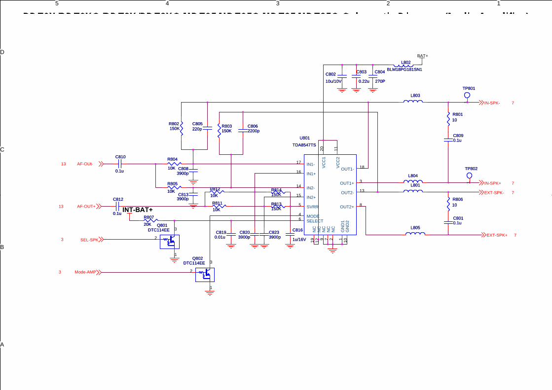
5 4 3 2 1
D
C
B
A A
BAT+
INT-BAT+
Mode-AMP3
SEL-SPK3
AF-OUt-13
AF-OUT+13
IN-SPK+ 7
IN-SPK- 7
EXT-SPK- 7
EXT-SPK+ 7
C8010.1uC8010.1u
C810
0.1u
C810
0.1u
R81110KR81110K
R803150KR803150K
L801L801
C8062200pC8062200p
R80610R80610
R805
10K
R805
10K
C8090.1uC8090.1u
L805L805
U801
TDA8547TS
U801
TDA8547TS
VC
C1
20
VC
C2
11
IN1-17
IN1+16 OUT1- 18
OUT1+ 3IN2-14
IN2+15
SVRR5
MODE4SELECT6
GN
D1
1G
ND
210
OUT2+ 8
OUT2- 13
NC
2N
C7
NC
9N
C12
NC
19
TP801TP801
1
L803L803
C805220pC805220p
TP802TP802
1
R80110R80110
R804
10K
R804
10K
L804L804
L802
BLM18PG181SN1
L802
BLM18PG181SN1
R807
20K
R807
20K
R802150KR802150K
C8190.01uC819
0.01u
C802
10u/10V
C802
10u/10V
R814150KR814150K
C8083900pC808
3900p
C804
270P
C804
270P
DTC114EEQ802
DTC114EEQ802
3
1
2
R81210KR81210K
C8203900pC820
3900p
C816
1u/16V
C816
1u/16V
DTC114EEQ801
DTC114EEQ801
3
1
2
R813150KR813150K
C8133900pC813
3900p
C8233900pC8233900p
C803
0.22u
C803
0.22u
C812
0.1u
C812
0.1u

5 4 3 2 1
D
C
B
A A
LOAD-DAC
PD-DAC
5VRT
3V3DRF
MOD-XO 1
APC/TV1 1,14
MOD-VCO 1
MCBSP2-DX-DAC5MCBSP2-CLKX-DAC5MCBSP2-FSX-DAC5
TO VCO
TO VCTCXO
TP702APC/TV1TP702APC/TV1
1
C704470pC704470p
R71410kR71410k
R707
33kR707
33k
R713100R713100
R705 10K-FR705 10K-F
R712 BLM15AG121SN1
R712 BLM15AG121SN11 2
R701 1KR701 1K
C708150pC708150p
C703470PC703470P
U701TLV5614IPWU701TLV5614IPW
DV
DD
1P
D2
LDA
C3
DIN
4S
CLK
5C
S6
FS7
DG
ND
8R
EFI
NC
D10
AG
ND
9
RE
FIN
AB
15O
UTA
14O
UTB
13O
UTC
12O
UTD
11
AV
DD
16
C7011u/10vC7011u/10v
C7051000PC7051000P
R71110kR71110k
C7061uC7061u
R704 100R704 100
R709
100k
R709
100k
C7100.1uC7100.1u
C712
1u
C712
1u
C7111u
C7111u
R70268kR70268k
R706 10K-FR706 10K-F
R710100kR710100k
TP701MOD2TP701MOD2
1
L702
BLM15AG121SN1
L702
BLM15AG121SN11 2
C7071uC7071u
C709120pC709120p

5
5
4
4
3
3
2
2
1
1
D D
C C
B B
A A
POWER-SW+
POWER-SW+
POWER-SW+
3V3D
1V6D
5VRT
3V3D
3V6D
5VFGU
BAT+
3V6D
1V8D
3V3A
BAT+ EXT-BAT+
3V3ARFBAT+
3V3GPS
3V3DRF
3V3DRF
BAT+ INT-BAT+
3V3DRF
PS-GPS3
PWR-RESET2
PWR-SW+ 6,7
PWR-SW- 6,7,12,13
EXT-PWR 3
POWER-CTL 3
POWER-KEY-DET 3
POWER-CTL 3
Maximal current 500mA
C676
0.22uF 10V
C676
0.22uF 10V C6012.2uFC6012.2uF
R628 47KR628 47K
C6503900PC6503900P
C6040.1uF/16V
C6040.1uF/16V
C6780.22uF 10VC678
0.22uF 10V
C6830.22uFC6830.22uF
C612
0.01uF*NC
C612
0.01uF*NC
U607TPS3808G33QDBVRQ1
U607TPS3808G33QDBVRQ1
RESET1
MR3 GND2Ct 4
VDD 6SENSE 5
U608RP102N331B
U608RP102N331B
VDD1GND2CE3 NC 4
VOUT 5
C616100pFC616100pF
C620100pF/16V
C620100pF/16V
C66010uFC66010uF
D602D602
21
L601
BLM18PG181SN1
L601
BLM18PG181SN1
C619C619
C6710.1uFC6710.1uF
L613L613
R632 1KR632 1K
C6843900PC6843900P
L616L616
TP6041.8VTP6041.8V
1
C606
2.2uF
C606
2.2uF
U605
TK11250CM
U605
TK11250CMON
/OFF
1G
ND
2N
P(V
RE
F)3
VIN
6G
ND
5V
OU
T4
C679
0.1uF/16V
C679
0.1uF/16V
D601D601
12
U601U601
RUN1
SYNC7
VFB3
PLLPF8
ITH2 GN
D4
VIN
6
SW 5 C685470PC685470P
C6873900PC6873900P
F602
1206L050-C
F602
1206L050-C
1 2
C6400.22UF 10V
C6400.22UF 10V
C641
2.2uF
C641
2.2uF
C6242.2uFC6242.2uF
U612RP102N331B
U612RP102N331B
VDD1GND2CE3 NC 4
VOUT 5
C6080.1uF*NCC6080.1uF*NC
+ C63747u
+ C63747u
12
U609RP102N331B
U609RP102N331B
VDD1GND2CE3 NC 4
VOUT 5
U611U611
RUN1
SYNC7
VFB3
PLLPF8
ITH2 GN
D4
VIN
6
SW 5
Q605
SI2307BDS
Q605
SI2307BDS
1
23
C6250.1uFC6250.1uF
R625
100K
R625
100K
D604DAN222
D604DAN222
1
23
C6034.7uF/16V*NC
C6034.7uF/16V*NC
C6180.1uF/16VC6180.1uF/16V
C636C636
11 2 233
L610L610
C617
0.1uF/16V
C617
0.1uF/16V
C681
470P
C681
470P
C6863900PC6863900P
C680
470P
C680
470P
L612
BLM18PG181SN1
L612
BLM18PG181SN1
C6580.1uF/16V
C6580.1uF/16V
Q608
2SK1824
Q608
2SK18242
31
C639
0.1uF
C639
0.1uF
C6294.7uF/16V
C6294.7uF/16V
C659
0.1uF
C659
0.1uF
C611
0.1uF*NC
C611
0.1uF*NC
L611
BLM18PG181SN1
L611
BLM18PG181SN1
R627 47KR627 47K
C657C657
11 2 233
C654C654
11 2 233
Q603*NCQ603*NC
1
32
C67010uFC67010uF
R620
100K
R620
100K
L614L614
C6150.1u/16VC615
0.1u/16V
C602100pF/16V
C602100pF/16V
C64910uFC64910uF
P606P606
1
C646C646
11 2 233
C6300.1uF/16V
C6300.1uF/16V
C6623900PC6623900P
C6350.1uFC6350.1uF
U604
TK11250CM
U604
TK11250CM
ON
/OFF
1G
ND
2N
P(V
RE
F)3
VIN
6G
ND
5V
OU
T4
C682
0.1uF/16V
C682
0.1uF/16V
Q606
SI1013R
Q606
SI1013R
1
23
C609
1uF*NC
C609
1uF*NC
C6280.22UF 10V
C6280.22UF 10V
R622R622
Q607
2SK1824
Q607
2SK18242
31
C6383900P
C6383900P
C651
0.01uF
C651
0.01uF
C613NC
C613NC
R631 15KR631 15K
C656
0.1uF
C656
0.1uF
R629 2.7KR629 2.7K
C668
0.01uF
C668
0.01uF
C666
3900
C666
3900
L615L615
TP6033.6VTP6033.6V
1
+ C66547u
+ C66547u
12
R630 47KR630 47K
C652470pFC652470pF
L603
BLM18PG181SN1
L603
BLM18PG181SN1
R615
NC
R615
NC
L602BLM18PG181SN1
L602BLM18PG181SN1
R626
100K
R626
100K
L606
BLM18PG181SN1
L606
BLM18PG181SN1
C627C627
11 2 233
J601
PD-700/BATB
J601
PD-700/BATB
12345
C645220P/50V
C645220P/50V
R607 10R607 10
R633
100K
R633
100K
R611
10K
R611
10K
L617
BLM18PG181SN1
L617
BLM18PG181SN1
C6420.1uFC6420.1uF
P608P608
1
P609P609
1
R623
100K-F
R623
100K-F
U603RP102N331B*NC
U603RP102N331B*NC
VDD1GND2CE3 NC 4
VOUT 5
C6145.6pFC6145.6pF
R624
100K
R624
100K
R612 1KR612 1K
C6532.2uFC6532.2uF
R62147KR62147K
L605BLM18PG181SN1
L605BLM18PG181SN1
R618130K-FR618130K-F
C647
0.01uF
C647
0.01uF
P610P610
1
C674220P/50V
C674220P/50V
Q604
2SK1824
Q604
2SK18242
31
TP602RESETTP602RESET
1
C6231uF/25VC6231uF/25V
TP6051.6VTP6051.6V
1
C688
0.1uF
C688
0.1uF
C6051uF/25VC605
1uF/25V
C6550.22UF 10V
C6550.22UF 10V
L604
BLM18PG181SN1*NC
L604
BLM18PG181SN1*NC
C672
20pF/50V
C672
20pF/50V
R617
470K-F
R617
470K-F
C6102.2uF*NCC6102.2uF*NC
C6214.7uF/16V
C6214.7uF/16V
L607L607
C6771uFC677
1uF
C669
1uF
C669
1uF
U606RP102N331B
U606RP102N331B
VDD1GND2CE3 NC 4
VOUT 5
R614R614
C648
1uF
C648
1uF
R613 1KR613 1K
C667C667
11 2 233
U610RP102N181D
U610RP102N181D
VDD1GND2CE3 NC 4
VOUT 5
F601
2.5A-32V
F601
2.5A-32V
1 2
L609
BLM18PG181SN1
L609
BLM18PG181SN1
C6260.1uF/16VC6260.1uF/16V
C644
20pF/50V
C644
20pF/50V
C663470pFC663470pF
R601
91K-F
R601
91K-F
P607P607
1
C661C661
11 2 233
C6220.1uF/16V
C6220.1uF/16V
C607
0.1uF
C607
0.1uF

5
5
4
4
3
3
2
2
1
1
D D
C C
B B
A A
SYNCB-IF
5VFGU
3V3DRF
3V3A
CLK-IF/PLL 1
CLK-OMAP/IF 2
IF14
PS-2LOC 3
SPI-DIN-IF 5
SPI-SCK-IF 5SPI-DOUT-IF 5SPI-CS2-IF 5
MCBSP2-FSR-IF 5
MCBSP2-CLKR-IF 5MCBSP2-DR-IF 5
TP413FERCLK
TP413FERCLK
1
R405 10KR405 10K
C464
0.1u
C464
0.1u
C4470.01uC4470.01u
D4021SV305
D4021SV3052
1
C44339PC44339P
C427
220p
C427
220p
C4312200pC4312200p
R4078.2KR4078.2K
Q4012SC4617
Q4012SC4617
2
31
R4094.7KR4094.7K
L403 BLM15AG121SN1L403 BLM15AG121SN11 2
C4650.1uC4650.1u
C451NCC451NC
C44833pC44833p
C428100PC428100P
C46133pC46133p
C4570.01uC4570.01u
C421ncC421nc
R412100kR412100k
C4490.01uC4490.01u
C435
0.1u
C435
0.1u
C429100PC429100P
L405
BLM15AG121SN1
L405
BLM15AG121SN1
1 2
C466
0.1u
C466
0.1u
C469
270P
C469
270P
R411390R411390
L4136.8UHL4136.8UH
C4400.01uC4400.01u
C45820pC45820p
C438100PC438100P
C450
0.012u
C450
0.012u
C43222pC43222p
TP403GNDTP403GND
1
C4527PC4527P
C470
270P
C470
270P
R403150RR403150R
R41010kR41010k
R408100R408100
C467
2.2u/10v
C467
2.2u/10v
L410BLM18AG601SN1
L410BLM18AG601SN1
C453 0.01uC453 0.01u
C441
0.1u
C441
0.1u
C459470PC459470P
C4620.1uC4620.1u
C4340.1uC4340.1u
R414 3.3kR414 3.3k
C471
270P
C471
270P
C4375600PC4375600P
C4722.2uFC4722.2uF
C42515pC42515p
R416820RR416820R
TP404CV2TP404CV2
1
C4220.1uC4220.1u
C42012PC42012P
R404
1.2KR404
1.2K
TP4012FLOTP4012FLO
1
R40151R40151
C439100PC439100P
R4131.8kR4131.8k
D401
HVC350B
D401
HVC350B21
C4540.01uC4540.01u
R4061KR4061K
C444470PC444470P
C4260.01uC4260.01u
L402
270n
L402
270n
L411 3.3uL411 3.3u
C423
1u
C423
1u
R415
10K
R415
10K
+C4680.68u/10v+
C4680.68u/10v
12
L412 BLM15AG121SN1L412 BLM15AG121SN11 2
C436
0.01u
C436
0.01u
C455
3300PC455
3300P
L407BLM15AG121SN1
L407BLM15AG121SN1
1 2
U401
AD9864
U401
AD9864
MXOP1MXON2GNDF3IF2N4IF2P5VDDF6GCP7GCN8VDDA9GNDA10VREFP11VREFN12
RR
EF13
VDD
Q14
IOU
TC15
GN
DQ
16VD
DC
17G
ND
C18
CLK
P19
CLK
N20
GN
DS
21G
ND
D22
PC23
PD24
PE 25VDDD 26VDDH 27CLKOUT 28DOUTA 29DOUTB 30FS 31GNDH 32SYNCB 33GNDS 34FREF 35GNDL 36
GN
DP
37IO
UTL
38VD
DP
39VD
DL
40C
XVM
41LO
N42
LOP
43C
XVL
44G
ND
I45
CXI
F46
IFIN
47VD
DI
48PRPAD 49
R40210kR40210k
C430
0.1u
C430
0.1u
C4564pC4564p
C46030pC46030p
Q402
UMC4N
Q402
UMC4N
1
2
34
5
C4420.01uC4420.01u
L40410uL40410u
Q4032SC3356
Q4032SC3356
2
31
L409
470nHL409
470nH
C4450.1uC4450.1u
L4084.7uL4084.7u
C4630.22uC463
0.22u
L40110uL40110u
C433
0.1u
C433
0.1u
L406220n(HQ)L406220n(HQ)
TP402IF
TP402IF
1
C4460.1uC4460.1u

5
5
4
4
3
3
2
2
1
1
D D
C C
B B
A A
MOT+
LED-K-LCD
IMO
LED-K-LCD
LED-K-KEY
LED-K-KEY
LED1LED2
PTT-KEY
LED1LED2
MOT-
3V3DRF
3V3D
3V3A
3V6D
3V3D3V6D
EXT-BAT+
VFLASH
3V3D
3V3DRF
CH1 3
CH2 3CH8 3
LED-IND1 3
INT-PTT 3
LED-IND2 3
CH4 3
UART1-RX-OPT/PS5,6
UART1-TX-OPT/PS5,6
EMERGENCY 3
KB-C1 5
MOTOR-CTL 3
IIC-SCL-Acce 5
KB-R0 5
KB-C0 5
IIC-SDA-Acce 5
Acce-INT1 3
PWR-SW+ 6,10PWR-SW- 6,10,12,13
VOL 13
KB-C05KB-C15KB-C25KB-C35KB-C45
/RST-OUT3/CS2-LCD 4M-A1 4
M-D2 4M-D34M-D4 4
M-D14 M-D0 4
/WE4 /OE 4
M-D74 M-D6 4M-D54
M-D134 M-D14 4M-D154
M-D8 4M-D94M-D10 4M-D114
M-D12 4
LED-LCD-BL 3 LED-KEY 3
USB-D- 5,6USB-D+ 5,6
EXT-SPK+ 12
EXT-SPK- 12
MCBSP3-DX-OPT 5
MCBSP3-DR-OPT 5MCBSP3-CLK-OPT 5
MCBSP3-FSX-OPT 5
UART3-RTS/IO29-OPT5UART3-CTS/IO30-OPT5
UART3-TX-OPT5UART3-RX-OPT5
IO1-OPT3IO2-OPT3IO3-OPT3
IN-SPK-12
IN-SPK+12
IO5-OPT3IO4-OPT3
INT-MIC-780 13INT-MIC+780 13
EXT-MIC-13
EXT-MIC+13
SEL2-Accessory 3SEL3-Accessory 3
EMERGENCY 3KB-R1 5KB-R2 5KB-R3 5KB-R4 5
SEL1-Accessory 3,13
IO-TD-TEST3
AF-CODEC-TO-50PINAF-50PIN-TO-CODEC
EXT-PTT 3
IIC-SCL-Acce 5
IIC-SDA-Acce 5
IIC-INT 5
IIC-SCL-Acce 5IIC-SDA-Acce 5
U317U317
X1 A1X2 A2X3 A3X4 A4X5 A5X6 A6
Y1C1Y2C2Y3C3Y4C4Y5C5Y6C6
GN
D1
B1
GN
D2
B2
GN
D3
B3
C315
470p
C315
470p
D309D3092 1
D318D3181
543 2
6
Q310
BSH103
Q310
BSH103
1
32
U318U318
X1 A1X2 A2X3 A3X4 A4X5 A5X6 A6
Y1C1Y2C2Y3C3Y4C4Y5C5Y6C6
GN
D1
B1
GN
D2
B2
GN
D3
B3
R323
2.2K
R323
2.2K
J313
JST SM02B-SRSS-TB(LF)
J313
JST SM02B-SRSS-TB(LF)
12
D310D3102 1
C319
100k
C319
100k
C331
470P
C331
470P
C322
270P
C322
270P
C334270pC334270p
L305BLM18AG601SN1
L305BLM18AG601SN1
U313U313
X1 A1X2 A2X3 A3X4 A4X5 A5X6 A6
Y1C1Y2C2Y3C3Y4C4Y5C5Y6C6
GN
D1
B1
GN
D2
B2
GN
D3
B3
U314U314
X1A1X2A2X3A3X4A4X5A5X6A6
Y1 C1Y2 C2Y3 C3Y4 C4Y5 C5Y6 C6
GN
D1
B1
GN
D2
B2
GN
D3
B3
C335
470P
C335
470P
P312P312 1
J1601
AXK6F50347YG
J1601
AXK6F50347YG
1234567891011121314151617181920212223242526272829303132333435363738394041424344454647484950
D302
1N4148WS
D302
1N4148WS
12
U316U316
X1 A1X2 A2X3 A3X4 A4X5 A5X6 A6
Y1C1Y2C2Y3C3Y4C4Y5C5Y6C6
GN
D1
B1
GN
D2
B2
GN
D3
B3
L303BLM18PG181SN1
L303BLM18PG181SN1
R331R331
R330R330
R321
3.01
R321
3.01
R324 33R324 33
L304BLM18AG601SN1
L304BLM18AG601SN1
J311
DF12E(3.0)-30DP-0.5V(81)
J311
DF12E(3.0)-30DP-0.5V(81)
1 23 45 67 89 10
11 1213 1415 1617 1819 2021 2223 2425 2627 2829 30
P314P314 1
C318
0.1u
C318
0.1u
R329R329
U312U312
X1A1X2A2X3A3X4A4X5A5X6A6
Y1 C1Y2 C2Y3 C3Y4 C4Y5 C5Y6 C6
GN
D1
B1
GN
D2
B2
GN
D3
B3
C324
470P
C324
470P
C332
470P
C332
470P
C321
270P
C321
270P
D305D305
2 1
C313
470p
C313
470p
R325 33R325 33
C3100.1uC3100.1u
U320U320
X1A1X2A2X3A3X4A4X5A5X6A6
Y1 C1Y2 C2Y3 C3Y4 C4Y5 C5Y6 C6
GN
D1
B1
GN
D2
B2
GN
D3
B3
R318100KR318100K
D306D306
2 1
P313P313 1
U310
NC*MMA7455L
U310
NC*MMA7455L
DVdd_IO1GND2NC3IADDR04GND15AVdd6CS7 INT1/DRDY 8INT2 9NC1 10RFU 11SDO 12SDA/SDI/SDO 13SLC/SPC 14
P311P311 1
R317 10KR317 10K
D304D304
21
C323
1u
C323
1u
C333
470P
C333
470P
R3153.3KR3153.3K
C3141uC3141u
R326 33R326 33
Q313
BSH103
Q313
BSH1031
32
R316 10KR316 10K
R3143.3KR3143.3K
C3121u
C3121u
C336
470P
C336
470P
R322
2.2K
R322
2.2K
DTC114EEQ312
DTC114EEQ312
3
1
2
U315U315
X1 A1X2 A2X3 A3X4 A4X5 A5X6 A6
Y1C1Y2C2Y3C3Y4C4Y5C5Y6C6
GN
D1
B1
GN
D2
B2
GN
D3
B3
J821
AXK5F16547YG
J821
AXK5F16547YG
12345678910111213141516
L302BLM18AG601SN1
L302BLM18AG601SN1
TP301TP301
1
D307D30721
U321U321
X1A1X2A2X3A3X4A4X5A5X6A6
Y1 C1Y2 C2Y3 C3Y4 C4Y5 C5Y6 C6
GN
D1
B1
GN
D2
B2
GN
D3
B3
U319U319X1A1 X2A2 X3A3 X4A4 X5A5 X6A6
Y1 C1Y2 C2Y3 C3Y4 C4Y5 C5Y6 C6
GN
D1
B1
GN
D2
B2
GN
D3
B3
C326
270p
C326
270p
C320
470p
C320
470p
C317
470p
C317
470p
C316
470p
C316
470p
P310P310 1
U322U322
X1A1X2A2X3A3X4A4X5A5X6A6
Y1 C1Y2 C2Y3 C3Y4 C4Y5 C5Y6 C6
GN
D1
B1
GN
D2
B2
GN
D3
B3
D308D30821
D303D303
21
C325
270p
C325
270p
C311
0.1u
C311
0.1u

5
5
4
4
3
3
2
2
1
1
D D
C C
B B
A A
3V3D
3V3D
3V3D
MCBSP3-DX-OPT7MCBSP3-DR-OPT7
KB-R2 7
IIC-SDA-Acce7
SPI-DIN-IF8
UART3-RTS/IO29-OPT 7
KB-R3 7
uW-SDO-CODEC13
UART3-CTS/IO30-OPT 7
KB-R0 7
SPI-SCK-IF8
uW-SDI-CODEC13
UART3-TX-OPT 7
IIS-BLCK-CODEC13
KB-C1 7
UART3-RX-OPT 7
SPI-DOUT-IF8
MCBSP3-CLK-OPT7
IIS-WCLK-CODEC13
KB-C2 7
MCBSP3-FSX-OPT7
KB-C3 7
IIS-DI-CODEC13
KB-C4 7
IIS-DO-CODEC13
IIC-SCL-Acce7
KB-R4 7
KB-C0 7
KB-R1 7
EMU1 6
TDO 6
/TRST 6TMS 6TDI 6
RTCK 6TCK 6EMU0 6
UART2-RX-GPS 9UART2-TX-GPS 9
USB-D+ 6,7USB-D- 6,7
MCBSP2-CLKR-IF8MCBSP2-FSR-IF8MCBSP2-DR-IF8
MCBSP2-CLKX-DAC11MCBSP2-FSX-DAC11MCBSP2-DX-DAC11
MCSI-CS-PLL1MCSI-CLK-PLL1
MCSI-DO-PLL1
SPI-CS2-IF8
uW-CLK-CODEC13uW-CS3-CODEC13 UART1-TX-OPT/PS 6,7
UART1-RX-OPT/PS 6,7
C260
560P
C260
560P
C270
270P
C270
270P
R25810KR25810K
C269
470P
C269
470P
C272
47P
C272
47P
R226 100R226 100
C261
560P
C261
560P
TP269TP269
1
C271
47P
C271
47P
TP264TP264
1R259 33R259 33
TP255TP255
1
C299
470P
C299
470P
R25610KR25610K
C262
270P
C262
270P
C293470PC293470P
TP263TP263
1
R255 33R255 33
TP260TP260
1
C286
47P
C286
47P
C273
47P
C273
47P
C263
470P
C263
470P
RN26122K*2RN26122K*2
1 234
C279
47P
C279
47P
C294470PC294470P
R222 100R222 100
C266470PC266470P
R262
15K
R262
15K
C291270PC291270P
RN25610K*4RN25610K*4
1 2 3 45678
C265
100P
C265
100P
R224 100R224 100
R261
15K
R261
15K
R22333
R22333
C264
470P
C264
470P
C296
470P
C296
470P
OMAP5912ZZG-1U201B
OMAP5912ZZG-1U201B
MCBSP1.CLKX/GPIO54G21 MCBSP1.FSX/GPIO53H15
MCBSP1.DX/GPIO52H18MCBSP1.DR/GPIO51H20
SPIF.DIN/GPIO47/uWIRE.SDIU18 SPIF.DOUT/GPIO46/uWIRE.SDOW21
MCBSP3.DX/GPIO43/MCSI1.CLKP14 MCBSP3.CLKX/GPIO42W16
MCSI1.DOUT/GPIO18W14
MCBSP3.FSX/GPIO12/TIMER.EXTCLKN18
MCSI1.SYNC/GPIO9W8 MCSI1.CLK/GPIO7M15
SPIF.CS2/MPUIO4/uWIRE.CS2/LED2T19SPIF.SCK/MPUIO1U19
MCBSP3.DR/MCSI1.SYNCAA17
I2C.SCLT18I2C.SDA/GPIO48V20
MCBSP2.CLKR/GPIO11V7
MCBSP2.CLKX/GPIO20Y6
MCBSP2.FSR/GPIO12W6
MCBSP2.FSX/GPIO21W7
MCBSP2.DR/GPIO19AA5
MCBSP2.DX/GPIO22P10
KP.R0/MPUIO8 G18KP.R1/MPUIO9 F19
KP.R2/MPUIO10 H14KP.R3/MPUIO13 E20KP.R4/MPUIO15 E19
KB.C0/MPUIO0 F18KB.C1/MPUIO6 D20KB.C2/GPIO61 D19KB.C3/GPIO63 E18KB.C4/GPIO27 C21
uWIRE.SDI/GPIO33J14 uWIRE.SDO/GPIO57H19 uWIRE.SCLK/GPIO39J15
NC
E5
NC
L1
UART1.RX/UART1.IRRX/GPIO37 V14UART1.TX/UART1.IRTX Y14
UART2.RX/GPIO18 R9UART2.TX/GPIO17 V6
UART3.RTS/GPIO29 K14UART3.CTS/GPIO30 K15UART3.RX/GPIO31 K19UART3.TX/GPIO32 K18
USB.DM/I2C.SCL/UART1.TX/Z R8USB.DP/I2C.SDA/UART1.RX P9
USB.PUEN W4
TRST Y18TMS V17TDI Y19TDO AA19RTCK Y17TCK W18EMU0 V16EMU1 W17
LCD
.P0
D18
LCD
.P1
B21
LCD
.P2
C19
LCD
.P3
G14
LCD
.P4
H13
LCD
.P5
A20
LCD
.P6
B19
LCD
.P7
C18
LCD
.AC
B15
LCD
.HS
C20
LCD
.PC
LKC
15LC
D.V
SB
18
uWIRE.CS3/GPIO34/CAM.D6J19
C285
270P
C285
270P
TP258TP258
1
TP266TP266
1
TP267TP267
1
C256
470P
C256
470P
C290
270P
C290
270P
TP265TP265
1
TP262TP262
1
C259470PC259
470P
R257 100R257 100
R220 100R220 100
C292270PC292270P
R225 100R225 100
TP259TP259
1
TP261TP261
1
C268
470P
C268
470P
R221 100R221 100
C258
470P
C258
470P
C274
12P
C274
12P
R260 1.5KR260 1.5K
C257
470P
C257
470P
C255
470P
C255
470P
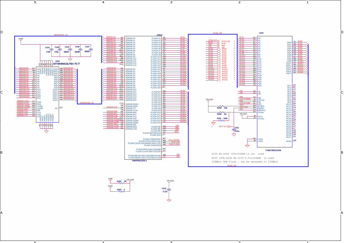
5
5
4
4
3
3
2
2
1
1
D D
C C
B B
A A
M-D13M-D14M-D15
/UB/LB
/RST-OUT
/CS3-FLASH
M-D8
SDRAM.A10
M-A9
SDRAM.D10
SDRAM.D7
M-A10
SDRAM.CKE
SDRAM.A3
SDRAM.D0
/OE
M-D7
SDRAM.BA1
SDRAM.A[0..12]
SDRAM.A11 SDRAM.D11
M-A11
SDRAM.D8
M-A12
SDRAM.A4
SDRAM.BA0
M-A1
/CS3-FLASH
M-D8
SDRAM.D12
SDRAM.D9
SDRAM.LDQMSDRAM.D[0..15]
SDRAM.A5
M-A13
SDRAM.CS#
SDRAM.D10
SDRAM.D13
M-A14
SDRAM.A0
M-D9
RDYSDRAM.UDQM
M-D9
M-A2
SDRAM.A6
/OE
RDY/WP/WE
SDRAM.D11
SDRAM.D14
SDRAM.A1
M-A[1..24]
M-A15
M-D0
M-D10SDRAM.WE#
M-A16
SDRAM.A7
SDRAM.CLK
SDRAM.D12
SDRAM.CAS#
SDRAM.A12
SDRAM.D15
SDRAM.A2
SDRAM.CLK
M-A1/WE/OEM-D0M-D1M-D2M-D3M-D4M-D5M-D6M-D7
M-D1
M-D11
SDRAM.D1
/WP
SDRAM.A8
SDRAM.D13
M-A17SDRAM.D2
SDRAM.A3M-A18
SDRAM.D0
SDRAM.CKE
M-D2SDRAM.D14
M-D12
SDRAM.A9
SDRAM.D3
M-A3
SDRAM.A4
SDRAM.D1
SDRAM.RAS#
M-A19
M-A4
SDRAM.D15
SDRAM.CS#
M-A20SDRAM.D4
SDRAM.A10
SDRAM.CAS#
M-D13
SDRAM.D2
SDRAM.A5
SDRAM.WE#
SDRAM.D5
M-A5
SDRAM.A11
SDRAM.RAS#
M-A21
M-D14
SDRAM.A6
SDRAM.LDQM
M-D3
SDRAM.A0
/CS2-LCD
SDRAM.D6
SDRAM.A12
M-A6
/CS2-LCD
SDRAM.D3
M-A22
/LB
SDRAM.A7
M-D15
M-D10
SDRAM.UDQM
M-D4
SDRAM.D7
SDRAM.BA0
SDRAM.D4
M-A7
SDRAM.A8M-A23
SDRAM.D8
/WE
M-D5
SDRAM.D5
SDRAM.A1
SDRAM.BA1
M-A8
SDRAM.A9M-A24
SDRAM.D9
M-D[0..15]
SDRAM.D6
SDRAM.A2
M-D6
/CS1-PsRAM
M-D11
/UB
M-D15
/CS1-PsRAM
M-D12
M-A1M-A2M-A3M-A4M-A5M-A6M-A7M-A8M-A9M-A10M-A11M-A12M-A13M-A14M-A15M-A16M-A17M-A18M-A19M-A20M-A21M-A22M-A23M-A24
M-D0M-D1M-D2M-D3M-D4M-D5M-D6M-D7M-D8M-D9M-D10M-D11M-D12M-D13M-D14
VFLASH
1V8D
VFLASHVFLASH1V8D
3V3D
VFLASH
M-D13 7M-D14 7M-D15 7
M-D8 7M-D9 7
/CS2-LCD 7
M-D1 7
M-D4 7M-D3 7M-D2 7
M-D6 7M-D5 7
M-D7 7
M-D0 7
M-A1 7/WE 7/OE 7
M-D10 7M-D11 7M-D12 7
/RST-OUT2
R236 100k,R246 NF,C239 0.01u:PsRAM is used
128Mbit NOR Flash ,can be extended to 256Mbit
R236 NF,R246 100k:PsRAM is not used
U244
TV00570002CDGB
U244
TV00570002CDGB
A0G1A1F1A2E1A3D1A4F2A5E2A6D2A7C2A8C6A9E6A10F6A11C7A12D7A13E7A14F7A15D8A16G8A17F3A18E3A19D6A20E5A21E8A22F8A23F5
DQ0 J2DQ1 G3DQ2 K3DQ3 H4DQ4 H5DQ5 K6DQ6 G6DQ7 J7DQ8 K2DQ9 H3
DQ10 J3DQ11 K4DQ12 J6DQ13 H6DQ14 K7DQ15 H7
CEfH1 OEH2
RESETD4WP/ACCC4
VCCfJ4
CE1-psJ1
RY/BYfE4
NC1 A1NC2 B1NC3 C1NC4 L1NC5 M1NC6 B2NC7 L2NC8 B3
UBD3 LBC3
WEC5
CE2psD5
VCCpsJ5
NC9 L3NC10 B4NC11 F4NC12 G4NC13 L4NC14 B5NC16 G5NC17 K5NC18 L5NC19 B6
NC22 G7NC23 L7NC24 A8
VSS1G2VSS2J8
NC25 B8
NC21 B7NC20 L6
NC26 H8NC27 L8
NC28 M8
R249 10KR249 10K
C245
3900P
C245
3900P
C247
3900P
C247
3900P
C251
0.01u
C251
0.01u
C242
0.22u
C242
0.22u
OMAP5912ZZG-1
U201A
OMAP5912ZZG-1
U201A
FLASH.A1 J8FLASH.A2 D3FLASH.A3 C1FLASH.A4 E4FLASH.A5 D2FLASH.A6 F4FLASH.A7 E3FLASH.A8 J7FLASH.A9 F3
FLASH.A10 G4FLASH.A11 G3FLASH.A12 G2FLASH.A13 K8FLASH.A14 H4FLASH.A15 H3FLASH.A16 K7FLASH.A17 J2FLASH.A18 J4FLASH.A19 J3FLASH.A20 F2FLASH.A21 L8FLASH.A22 K4FLASH.A23 K3FLASH.A24 L7FLASH.A25 E1
FLASH.D0 N4FLASH.D1 N2FLASH.D2 N7FLASH.D3 P2FLASH.D4 P4FLASH.D5 P7FLASH.D6 R2FLASH.D7 R3FLASH.D8 R4FLASH.D9 T2
FLASH.D10 T3FLASH.D11 P8FLASH.D12 U1FLASH.D13 U3FLASH.D14 T4FLASH.D15 V3
FLASH.CLK/FLASH.CS2UOE N3
FLASH.RDY/GPIO10 V2FLASH.ADV L4
FLASH.CS2/FLASH.BAA/FLASH.CS2L M4
FLASH.BE1/FLASH.CS2UWE/GPIO60 M8FLASH.BE0/FLASH.CS2UOE/GPIO59 L3
FLASH.CS0/GPIO62 M7FLASH.CS1/FLASH.CS1L M3
FLASH.CS3/GPIO3 N8
FLASH.OE U4
FLASH.RP/FLASH.CS2UWE W1
FLASH.WE W2FLASH.WP V4
SDRAM.CSG8
SDRAM.DQSHC14SDRAM.DQSLD4
SDRAM.CASB4
SDRAM.DQMLC8 SDRAM.DQMUD10
SDRAM.RASH7 SDRAM.WEH8
SDRAM.A13H11 SDRAM.A12H9 SDRAM.A11H10 SDRAM.A10B8 SDRAM.A9B12 SDRAM.A8G9 SDRAM.A7G11 SDRAM.A6G12 SDRAM.A5B9 SDRAM.A4G10 SDRAM.A3A1 SDRAM.A2B6 SDRAM.A1B2 SDRAM.A0A2
SDRAM.BA1C3 SDRAM.BA0B3
SDRAM.D15C12 SDRAM.D14D12 SDRAM.D13D13 SDRAM.D12C11 SDRAM.D11C13 SDRAM.D10D11 SDRAM.D9D14 SDRAM.D8C10 SDRAM.D7D8 SDRAM.D6C4 SDRAM.D5C7 SDRAM.D4D5 SDRAM.D3D7 SDRAM.D2C5 SDRAM.D1C6 SDRAM.D0D6
SDRAM.CLKC9
SDRAM.CLKXD9
SDRAM.CKEH12
U242MT48H8M16LFB4-75 IT
U242MT48H8M16LFB4-75 IT
DQ0 A8DQ1 B9DQ2 B8DQ3 C9DQ4 C8DQ5 D9DQ6 D8DQ7 E9DQ8 E1DQ9 D2
DQ10 D1DQ11 C2DQ12 C1DQ13 B2DQ14 B1DQ15 A2
A0H7A1H8A2J8A3J7A4J3A5J2A6H3A7H2A8H1A9G3
A11G2A12G1
A10H9
CKEF3
RASF8
UDQMF1
BA1G8 BA0G7
WEF9
CASF7
LDQME8
CSG9
VS
SA
1A
1V
SS
J1J1
VS
SE
3E
3V
SS
QA
3A
3V
SS
QC
3C
3V
SS
QB
7B
7V
SS
QD
7D
7
VD
DE
7E
7V
DD
A9
A9
VD
DJ9
J9
NC E2
CLKF2
VD
DQ
B3
B3
VD
DQ
D3
D3
VD
DQ
A7
A7
VD
DQ
C7
C7
R248 NCR248 NC
C246
3900P
C246
3900P
R251 100kR251 100k
R253 NCR253 NC
C243
470P
C243
470P
R254 0R254 0
C244
470p
C244
470p

5
5
4
4
3
3
2
2
1
1
D D
C C
B B
A A
3V3D
EXT-PWR 10
PS-RXVCO1
SEL2-Accessory7
SEL-MIC12
SEL3-Accessory7
Mode-AMP 12
LED-LCD-BL7
TONE-CODEC13
LED-IND2 7
POWER-CTL 10
PLL-LD1
PS-TXVCO1
PS-GPS 10
MOTOR-CTL 7
LED-KEY 7
PS-RX14
CH1 7
INT-PTT 7
DAV-CODEC13
PS-APC 14
CH2 7
LED-IND1 7
CH8 7
CH4 7
Acce-INT1 7
RESET-CODEC13
SEL1-Accessory7
DISCHARGE-SW-TX 14
PS-2LOC8
IO1-OPT7
IO2-OPT7
IO3-OPT7
IO5-OPT7
IO4-OPT7
SEL1-ADC13
SEL2-ADC13
EXT-PTT 7
POWER-KEY-DET 10
EMERGENCY 7
SW-CVread 1
IO-TD-TEST 3
PS-TX14
SW-CHARGE-FGU 1
SEL-SPK 3
IIC-INT5
del:R242、R244
C281 470PC281 470P
C295470PC295470P
C284 470PC284 470P
R263
470
R263
470
C288470PC288470P
C275
1500p
C275
1500p
C280 470PC280 470P
C276
1500p
C276
1500p
U201D
OMAP5912ZZG-1
U201D
OMAP5912ZZG-1
GPIO1/UART3.RTS R19
GPIO13/LCD.BLUE0 N19
MPUIO5/LOW_PWR/UART3.RTS T20
GPIO40/BCLKREQ W15
GPIO23/MCLKREQ R10
GP
IO55
/RTC
_WA
KE
_IN
TW
13MPUIO11 W10
GPIO25/MCSI2.DOUT W9
GPIO0/USB.VBUSR18
MP
UIO
5/M
PU
IO12
W5
MPUIO3/MMC2.DAT1 V8
GP
IO7/
MC
SI2
.SY
NC
V9
MPUIO10/MPUIO7 V10
GPIO57/MMC.CLK V11
GPIO8/TRST Y8
GPIO26/MCSI2.DIN AA9
GPIO27 Y10
GPIO55/MMC.CMD P11
MPUIO9/MPUIO6 W11
GPIO58 R11
GPIO6/MCSI1.DIN/TIMER.EVENT3P19
GPIO4/SPIF.DIN/TIMER.EVENT4P20
GPIO29/LCD.P8D17
GPIO30/LCD.P9D16
GPIO31/LCD.P10C17
GPIO32/LCD.P11B17
GPIO33/LCD.P12G13
GPIO34/LCD.P13A17
GP
IO35
/LC
D.P
14C
16
GP
IO2/
LCD
.P15
D15
GPIO14/LCD.RED0N21
MPUIO1/uWIRE.SCLK V19GPIO2M14
GPIO39/UART1-IRSHDN AA15
GP
IO38
/UA
RT1
-IRS
EL
R14
GPIO62/MCBSP1.CLKSG20
MPUIO12/CAM.D0 L19
GPIO35/CAM.D7/UWIRE.CS0J18
GPIO38/CAM.HSL15
GPIO37/CAM.RSTZM19
MPUIO14/CAM.VS L18
GPIO50/PWT/TIMER.PWM0M18
GPIO15/TIMER.PWM2M20
GPIO49/PWL/TIMER.PWM1L14
GPIO3/MCBSP3.FSX/LED1P18
GPIO11/HDQN20
GPIO7/UART2.RCV Y5
GPIO16/FLASH.CS1U Y1
GPIO5/FLASH.CS2U P3
GPIO45/SPIF.CS0/UART3.TX/MCBSP3.CLKXN14
GPIO44/uWIRE.CS3P15
GPIO56/MCSI1.DIN V15
MPUIO2/SPIF.CS1/uWIRE.CS1 N15
GPIO28/KB.C5G19
C304
1500p
C304
1500p
R264 470R264 470
C283 470PC283 470P
R24110KR24110K
R242
10K
R242
10K
C298 470PC298 470P
C303470PC303470P
C277
1500P
C277
1500P
C282 470PC282 470P
R265 470R265 470
C287 470PC287 470P
C278 470PC278 470P
C289
1500P
C289
1500P
C305470PC305470P
C302470PC302470P
C300470PC300470P
C297470PC297470P
TP240TP240
1
C301470PC301470P

1
A A
3V3D
1V8D
1V8D
1V6D
1V6D
3V3D
3V3D
3V3D
3V3DRF
VFLASH
VFLASH
1V6D
1V6D
1V6D
3V3D3V3D
3V3D
CLK-CODEC13
PWR-RESET10
/RST-OUT4
CLK-OMAP/IF8
C2393900pC239
3900p
C2120.22uC2120.22u
C2413900pC2413900p
C210
0.22UF 10V
C210
0.22UF 10V
C2260.22uC2260.22u
C2130.22uC2130.22u
C208
330pC208
330p
C2313900PC2313900P
OMAP5912ZZG-1U201C
OMAP5912ZZG-1U201C
VS
SY
13
MPU_BOOTJ20
VSSP12
VS
SA
13V
SS
A21
VS
SB
1V
SS
B5
VS
SB
7V
SS
B16
VS
SF2
0V
SS
G1
VS
SK
2V
SS
K20
VS
SN
1V
SS
R21
VS
SU
2V
SS
W20
VS
SY
3V
SS
AA
1V
SS
AA
7V
SS
AA
21
CVDD A15CVDD M2CVDD Y9CVDD Y20
CVDD1 AA3CVDD2 A3CVDD2 A9CVDD2 E2
CVDD3 B13CVDD3 B20CVDD3 J21CVDD3 R20
CVDDRTC W12
CVDDDLL A11
CVDDA Y21
DVDD1 A19DVDD1 E21DVDD2 AA2DVDD3 Y7
DVDD4 A5DVDD4 A7DVDD4 B10DVDD4 B14
DVDD5 C2DVDD5 H2DVDD5 R1
DVDD6 AA11DVDD7 Y16DVDD8 L21DVDD9 U21
DVDDRTC V12
LDO.FILTER J1
CONFV18
RTC_ON_NOFFY12
OS
C32
K_O
UT
AA
13
OS
C32
K_I
NV
13
CLK
32K
_IN
P13
OS
C1_
OU
TW
3
OS
C1_
INY
2
MPU_RSTU20
PWRON_RESETR12
MCLK/GPIO24V5
BCLK/GPIO17Y15
CLK32K_OUT/GPIO36/MPUIO0/UART1-TXR13
BFAIL/EXT_FIQ/UART3.CTSW19
RST_OUT/GPIO41AA20
SYS_CLK_IN/UART2.BCLKY4
C214470PC214470P
C2061000PC2061000P
R206 10R206 10
C228470PC228470P
C232470PC232470PC236
1uC236
1u
R209 10R209 10
C215
0.01uF
C215
0.01uF
C2300.22uC2300.22u
C2490.22uC2490.22u
C207
270pC207
270p
R207 33R207 33
C2111000pC211
1000p
C2173900pC2173900p
C2333900PC2333900P
R208
0
R208
0
C237470PC237470P
C209
3900p
C209
3900p
C20320PC20320P
C2273900PC2273900P
C205ncC205nc
OE/ST
GND
OUT
VDD
X203
DSB321SDA
OE/ST
GND
OUT
VDD
X203
DSB321SDA
1
2
3
4
C2220.22uC2220.22u
C223
47P
C223
47P
C2180.22uC2180.22u
C2480.22uC2480.22u
C2380.22uC2380.22u
C2340.22uC2340.22u
C220470PC220470P
X201SSP-T7F 12.5pF 20ppm SEIKO
X201SSP-T7F 12.5pF 20ppm SEIKO
12 3
4L201 470nL201 470n
C204
20P
C204
20P
C2021000pC202
1000p
C2193900PC2193900P
C2210.22uC2210.22u
C2403900pC240
3900p
R203 10R203 10
C229
47P
C229
47P
C2160.22uC2160.22u

5
5
4
4
3
3
2
2
1
1
D D
C C
B B
A A
CV-out
CV-out
RF
charge
RF
charge
5VFGU
3V3DRF
5VFGU
3V3ARF
5VFGU
5VFGU
5VFGU
3V3ARF
RX-VCO-5V
3V3A
PS-RXVCO 3
MCSI-CS-PLL 5MCSI-CLK-PLL 5
MCSI-DO-PLL 5
PS-TXVCO 3
APC/TV111,14
SW-CHARGE-FGU5
CLK-IF/PLL 8
LO 14
PLL-LD3
SW-CVread3CV-ADC 13
MOD-XO 11
MOD-VCO 11
L121
BLM15AG121SN1
L121
BLM15AG121SN112
C1371000PC1371000P
R132220
R132220
TP108
PLLLD
TP108
PLLLD
1
C15182PC15182P
R108
3.3K
R108
3.3K
R113
470R
R113
470R
C181ncC181nc
C152
6.8p
C152
6.8p
R1108.2KR1108.2K
C157
0 Ohm
C157
0 Ohm
L11812nH
L11812nH
R143
3.3K
R143
3.3K
L109
BLM15AG121SN1
L109
BLM15AG121SN1
12
R1041KR1041K
L116470nHL116470nH
C1443.6pC1443.6p
R125
3.3K-F
R125
3.3K-F
Q108NE68519
Q108NE68519
2
31
C1611000pC1611000p
R1065.6KR1065.6K
Q106EMD22Q106
EMD22
1
2
43
6
5
C1246P
C1246P
U102
TC75W51FU
U102
TC75W51FU
A OUTPUT 1A -INPUT 2A +INPUT 3
V+8
B +INPUT5 B -INPUT6 B OUTPUT7
GND 4
Q104NE68519
Q104NE68519
2
31
C168100PC168100P
R130
10
R130
10
C1621000pF
C1621000pF
R13410R13410
R13856R13856
C1024p
C1024p
C11012pC11012p
R126nc
R126nc
D101BB208-2
D101BB208-2
21
C128 13pC128 13p
C1148PC1148P
C1820.1uC1820.1u
R121100R121100
C1650.1uC1650.1u
C1740.01uC1740.01u
TP103MOD-VCO
TP103MOD-VCO
1
C1098pC1098p
L108470nHL108470nH
C1066p
C1066p
R13310KR13310K
C1801000pC1801000p
L117
16nH
L117
16nH
R10310
R10310
C14822p
C14822p
C105
0.1u
C105
0.1u
C13020p
C13020p
Q1012SC5108Q1012SC5108
1
32
Q1022SC3356Q1022SC3356
2
31
C1034p
C1034p
C11612PC11612P
C1690.1uC1690.1u
L120
BLM15AG121SN1
L120
BLM15AG121SN1
12
L10139nL10139n
L113470nHL113470nH
R144
3.3K
R144
3.3K
C15312p
C15312p
+ C1852.2u/10v
+ C1852.2u/10v
12
C145 13pC145 13p
L10315nL10315n
L112
39nH
L112
39nH
R1188.2KR1188.2K
L10415nH(绕线)L10415nH(绕线)
C104470PC104470P
L124 470nL124 470n
D102 1SV305D102 1SV30521 D105
BA277D105BA277
12
C1210.1uC1210.1u
TP104RFCVTP104RFCV
1
Q103EMD22
Q103EMD22
1
2
43
6
5
D1071SV325
D1071SV325
21
R111
100
R111
100
TP101LF_control
TP101LF_control
1
C1591800p-KC1591800p-K
C136
470P
C136
470P
C154
2.2K-J
C154
2.2K-J
D108 BB208-2D108 BB208-221
C120470PC120470P
L10515nH(绕线)L10515nH(绕线)
Q105
2SC4617
Q105
2SC4617
2
31
C1254pC1254p
R146 33K-FR146 33K-F
R147
1K
R147
1K
C1670.1u
C1670.1u
C1561000PC1561000P
U101FSA 66
U101FSA 66
Vin 1OUT 2GND 3
Vcc5
ON/OFF4
C176
330pC176
330p
C111
4.7P
C111
4.7P
C1660.1uC1660.1u
+C1780.1u
+C1780.1u
12
C1831000pC1831000p
C146 13pC146 13p
TP106PLLCSTP106
PLLCS
1
R123 1K-FR123 1K-F
C132100PC132100P
R119
100
R119
100
L110330nHL110330nH
C1790.1uC1790.1u
C1158PC1158P
R109100kR109100k
C1293.6pC1293.6p
TP102VCOFBTP102VCOFB
1
C1402.2u/10vC1402.2u/10v
D109 BB208-2D109 BB208-221
R115150R115150
Q107EMD22Q107
EMD221
2
43
6
5
D1111SV279D1111SV279
21
TP107PLLCLK
TP107PLLCLK
1
D106
1SV325
D106
1SV325
21
C138
0.1u
C138
0.1u
L106470nHL106
470nH
C139
470P
C139
470P
R10510kR10510k
L119
470nH
L119
470nHR122
3.3k-J
R122
3.3k-J
D104BA277D104BA277
12
L114470nHL114
470nH
C1334.7P
C1334.7P
L10215nL10215n
R112180K
R112180K
D110BB208-2
D110BB208-2
21
C1260.1u
C1260.1u
C1710.75p
C1710.75p
C1631000p
C1631000p
R145
33K-F
R145
33K-F
C1640.1uC1640.1u
C142470PC142470P
R1164.7KR1164.7K
C123 13pC123 13p
C1721000PC1721000P
L10747nL10747n
C1410.1uC1410.1u
C11312P
C11312P
R131 10R131 10
R137NC
R137NC
C13427p
C13427p
C173100PC173100P
R10210KR10210K
C112
4.7P
C112
4.7P
C1078p
C1078p
C127470PC127470P
U103sky72310
U103sky72310
VCCecl/cml1Fvco_main2Fvco_main3
LD/PS_main4VCCcp_main5CPout_main6
N/C7Xtalacgnd/OSC8Xtalin/OSC9Xtalout/NC10VCCxtal11GNDXtal12 N/C 13N/C 14N/C 15N/C 16N/C 17
VCCdigital 19
Data 20CS 21Clock 22
N/C 23Mux_out 24
N/C 18
Pow
erP
AD
25
C170100PC170100P
C15810K-J
C15810K-J
R14210kR14210k
C1431.5P
C1431.5P
L11122nHL11122nH
L125
BLM15AG121SN1
L125
BLM15AG121SN112
R1173.3KR1173.3K
R1402.2kR1402.2k
C101470PC101470P
R10156RR10156R
L115470nHL115470nH
C117
0.1u
C117
0.1u
U104FSA 66U104FSA 66
Vin 1OUT 2GND 3
Vcc5
ON/OFF4
C1473.6pC1473.6p
D112BA277D112BA277
1 2
D103 1SV305D103 1SV30521
R124
3.3K-F
R124
3.3K-F
C11910pC11910p
R1204.7K-JR1204.7K-J
R107390RR107390R
L123
BLM15AG121SN1
L123
BLM15AG121SN1
1 2
C118
470P
C118
470P
C1225P
C1225P
C1492P
C1492P
R136
68R
R136
68R
L122BLM15AG121SN1
L122BLM15AG121SN1
12
C175
270pC175
270p
C1603300p-KC1603300p-K
R1271.2K-JR1271.2K-J
TP105PLLDATA
TP105PLLDATA
1
R12910KR12910K
VCC
OUT
VCONT
GND
X101
19.2MHZ
VCC
OUT
VCONT
GND
X101
19.2MHZ
1
23
4
R1143.3KR1143.3K
C1841000PC1841000P
R1283.9K-FR128
3.9K-F
C1088pC1088p
C1770.39uC1770.39u

5
5
4
4
3
3
2
2
1
1
D D
C C
B B
A A
3V3D
TMS 5TDI 5TDO 5RTCK 5TCK 5EMU0 5EMU1 5
USB-D- 5,7
/TRST 5
USB-D+ 5,7 PTT-IO 3USB
PD780 UHF Schematic Diagram(EXT Interface Circuit)
R3064.7K
R3064.7K
C307270pC307270p
J304NC*JTAG
J304NC*JTAG
1234567891011121314
R304100KR304100K
J302
nc-CON6
J302
nc-CON6
123456
D301
KPT-1608SURC
D301
KPT-1608SURC
1 2
R309 100R309 100
L301BLM15PD121SN1
L301BLM15PD121SN1
RN301 100*4RN301 100*4
12345
678
R305100KR305100K
R301100KR301100K
R308 4.7KR308 4.7KC306
0.1uC306
0.1u
RN302 100*4RN302 100*412345
678
R3074.7K
R3074.7K
C325270pC325270p
S302S30212

5
5
4
4
3
3
2
2
1
1
D D
C C
B B
A A
MIC-MIC+
PWR-SW-
INT-MIC+780
CH1
CH2
LED1
CH4
CH8VOL
LED2
INT-MIC-780
CH4CH4CH2
PWR-SW+PWR-SW-
PWR-SW+
LED2 VOL
VOL-HCH1CH8LED1 PWR-SW-
VOL-H
VOL-H
EMERGENCY
3V3DRF
1V8D-VOL
3V3DRF
3V3DRF
R
G
PD780 UHF Schematic Diagram(SW Board Circuit)
S1002S1002
12
3
45
C1001
270P
C1001
270P
B1001
OBE-27P42
B1001
OBE-27P42
+1-2
R1001 120R1001 120
C1003
270P
C1003
270P
D1005D1005
21
C1012
270P
C1012
270P
C1005
270P
C1005
270P
D1014D1014
21
S1003
EMERGENCY KEY
S1003
EMERGENCY KEY
123
4567
D1008D1008
21
C1010
270P
C1010
270P
D1013D1013
21
C1006
270P
C1006
270P
1C C4 2
8
S1001
1C C4 2
8
S1001
1234
56
D1003D1003
21
U1002RP102N181D
U1002RP102N181D
VDD1GND2CE3 NC 4
VOUT 5
C1016
0.1uF
C1016
0.1uF
D1006D1006
21
Q1001
UMG3N
Q1001
UMG3N
1
2
34
5
D1004D1004
21
U1001
CM1418-02CS
U1001
CM1418-02CS
A1
A2
A3B1
B2B3
C1008
270P
C1008
270P
D1002
12-22RG/TR8
D1002
12-22RG/TR8
12
3
D1009D1009
21R1002 120R1002 120
C10150.1uFC10150.1uF
D1011D1011
21
J1001AXK6F16547YG
J1001AXK6F16547YG
12345678910111213141516
D1007D1007
21
C1002
270P
C1002
270P
C1007
270P
C1007
270P
L1002
BLM18PG181SN1
L1002
BLM18PG181SN1
C1011
270P
C1011
270P
C10170.1uFC10170.1uF
D1001D1001
21
L1001
BLM18PG181SN1
L1001
BLM18PG181SN1
C1004
270P
C1004
270P

5
5
4
4
3
3
2
2
1
1
D D
C C
B B
A A
MIC-MIC+
PWR-SW-
INT-MIC+780
CH1
CH2
LED1
CH4
CH8VOL
LED2
INT-MIC-780
CH4CH4CH2
PWR-SW+PWR-SW-
PWR-SW+
LED2 VOL
VOL-HCH1CH8LED1 PWR-SW-
VOL-H
VOL-H
EMERGENCY
3V3DRF
1V8D-VOL
3V3DRF
3V3DRF
R
G
PD780 UHF Schematic Diagram(SW Board Circuit)
S1002S1002
12
3
45
C1001
270P
C1001
270P
B1001
OBE-27P42
B1001
OBE-27P42
+1-2
R1001 120R1001 120
C1003
270P
C1003
270P
D1005D1005
21
C1012
270P
C1012
270P
C1005
270P
C1005
270P
D1014D1014
21
S1003
EMERGENCY KEY
S1003
EMERGENCY KEY
123
4567
D1008D1008
21
C1010
270P
C1010
270P
D1013D1013
21
C1006
270P
C1006
270P
1C C4 2
8
S1001
1C C4 2
8
S1001
1234
56
D1003D1003
21
U1002RP102N181D
U1002RP102N181D
VDD1GND2CE3 NC 4
VOUT 5
C1016
0.1uF
C1016
0.1uF
D1006D1006
21
Q1001
UMG3N
Q1001
UMG3N
1
2
34
5
D1004D1004
21
U1001
CM1418-02CS
U1001
CM1418-02CS
A1
A2
A3B1
B2B3
C1008
270P
C1008
270P
D1002
12-22RG/TR8
D1002
12-22RG/TR8
12
3
D1009D1009
21R1002 120R1002 120
C10150.1uFC10150.1uF
D1011D1011
21
J1001AXK6F16547YG
J1001AXK6F16547YG
12345678910111213141516
D1007D1007
21
C1002
270P
C1002
270P
C1007
270P
C1007
270P
L1002
BLM18PG181SN1
L1002
BLM18PG181SN1
C1011
270P
C1011
270P
C10170.1uFC10170.1uF
D1001D1001
21
L1001
BLM18PG181SN1
L1001
BLM18PG181SN1
C1004
270P
C1004
270P

5
5
4
4
3
3
2
2
1
1
D D
C C
B B
A A
KB-C4
KB-C3
KB-C2
KB-C1
KB-C0
KB-R4
KB-R3
KB-R2
KB-R1
KEY-LED-K
VBUS
UART1-TX
UART1-RX
KB-C0
USB-D+
OPT-SEL1
KB-R4PTT
EXT-SPK-
KB-C3KB-C2
EXT-SPK+
KB-C1 OPT-SEL2OPT-SEL3
USB-D-
KB-C4KEY-LED-K
KB-R1EMERGENCY
EXT-MIC-EXT-MIC+
KB-R2KB-R3
IN-SPK+IN-SPK-
IN-SPK+
EXT-MIC+
IN-SPK-
UART1-TXUART1-RXEXT-MIC-
EXT-SPK+EXT-SPK-OPT-SEL3OPT-SEL2
USB-D-
OPT-SEL1PTTEMERGENCY
USB-D+
VBUS
3V6D
EXT-BAT+
3V6D
EXT-BAT+
BACK MENU UP
# 9 6 3 Cancel
0
*
8
7
5
4
2
1
DOWN
OK
IO to Vbus-Accessory
PD780 UHF Schematic Diagram(Keyboard Circuit)
S1703S1703
1 2
D1703D17031
5 432
6
S1715S1715
1 2
D1701D1701
1
5 432
6
R1705100R1705100
D1702D1702
1
5 432
6
D1706PESD12VS1UB
D1706PESD12VS1UB
21
R1702100R1702100
S1710S1710
1 2
D1723 PESD5V0S1UBD1723 PESD5V0S1UB
2 1
S1708S1708
1 2
D1717
19-2
13/W
1D-A
NP
HY
/3T
D1717
19-2
13/W
1D-A
NP
HY
/3T
12
R1708100R1708100
S1713S1713
1 2
D1711 PESD5V0S1UBD1711 PESD5V0S1UB21U1701CM1418-02CSU1701CM1418-02CS
A1
A2
A3B1
B2B3
S1718S1718
12
D1722 PESD5V0S1UBD1722 PESD5V0S1UB2 1
R1701 100R1701 100
J1702
MOLEX543630289
J1702
MOLEX543630289
1234567891011121314151617181920
S1702S1702
1 2
D1710 PESD5V0S1UBD1710 PESD5V0S1UB21
D1707PESD12VS1UB
D1707PESD12VS1UB
21
D1712 PESD5V0S1UBD1712 PESD5V0S1UB21
S1701S1701
12
S1707S1707
12
D1718
19-2
13/W
1D-A
NP
HY
/3T
D1718
19-2
13/W
1D-A
NP
HY
/3T
12
D1705PESD12VS1UB
D1705PESD12VS1UB
21
R1707100R1707100
R1704100R1704100
C1701 2.2uFC1701 2.2uF
S1706S1706
12
S1711S1711
12
S1704S1704
1 2
D1708PESD12VS1UB
D1708PESD12VS1UB
21
D1715
19-2
13/W
1D-A
NP
HY
/3T
D1715
19-2
13/W
1D-A
NP
HY
/3T
12
S1716S1716
12
S1709S1709
1 2
S1714S1714
1 2
D1719
19-2
13/W
1D-A
NP
HY
/3T
D1719
19-2
13/W
1D-A
NP
HY
/3T
12D1725 PESD5V0S1UBD1725 PESD5V0S1UB
2 1
J1701AXK5F50547YG 50pin
J1701AXK5F50547YG 50pin
1234567891011121314151617181920212223242526272829303132333435363738394041424344454647484950
R1706100R1706100
D1709PESD12VS1UB
D1709PESD12VS1UB
21
D1724
PESD5V0S1UB
D1724
PESD5V0S1UB
21
S1712S1712
1 2
R1703100R1703100
D1721 PESD5V0S1UBD1721 PESD5V0S1UB
2 1
D1716
19-2
13/W
1D-A
NP
HY
/3T
D1716
19-2
13/W
1D-A
NP
HY
/3T
12
D1714
19-2
13/W
1D-A
NP
HY
/3T
D1714
19-2
13/W
1D-A
NP
HY
/3T
12
S1717S1717
12
D1713 PESD5V0S1UBD1713 PESD5V0S1UB21
S1705S1705
1 2
D1720
19-2
13/W
1D-A
NP
HY
/3T
D1720
19-2
13/W
1D-A
NP
HY
/3T
12

Service Manual
186
12.7 Parts List Main Board for PD70X/ PD70XG/ PD78X/ PD78XG/ HD705/ HD705G/ HD785/ HD785G
No. Ref. No. Part No. Description
1 R208 3001050000000 0Ω
2 R254 3001050000000 0Ω
3 R9069 3001050000000 0Ω
4 C157 3001060000000 0Ω
5 C646 3001060000000 0Ω
6 C657 3001060000000 0Ω
7 C667 3001060000000 0Ω
8 L9039 3001060000000 0Ω
9 R9053 3099080398010 0.39Ω
10 R9054 3099080398010 0.39Ω
11 R9055 3099080398010 0.39Ω
12 R321 3099063018000 3.01Ω
13 R9005 3001055690000 5.6Ω
14 R103 3001051000000 10Ω
15 R130 3001051000000 10Ω
16 R131 3001051000000 10Ω
17 R134 3001051000000 10Ω
18 R203 3001051000000 10Ω
19 R206 3001051000000 10Ω
20 R209 3001051000000 10Ω
21 R801 3001051000000 10Ω
22 R806 3001051000000 10Ω
23 R607 3001061000000 10Ω
24 R9022 3001052200000 22Ω
25 R207 3001053300000 33Ω
26 R223 3001053300000 33Ω
27 R255 3001053300000 33Ω
28 R259 3001053300000 33Ω
29 R324 3001053300000 33Ω
30 R325 3001053300000 33Ω
31 R326 3001053300000 33Ω
32 R9009 3001053300000 33Ω
33 R9021 3001054700000 47Ω
34 R401 3001055100020 51Ω
35 R9075 3001055100020 51Ω
36 R101 3001055600000 56Ω
37 R9007 3001058200000 82Ω
38 L407 3001051010000 100Ω
39 R111 3001051010000 100Ω
40 R119 3001051010000 100Ω
41 R121 3001051010000 100Ω

Service Manual
187
No. Ref. No. Part No. Description
42 R220 3001051010000 100Ω
43 R221 3001051010000 100Ω
44 R222 3001051010000 100Ω
45 R224 3001051010000 100Ω
46 R225 3001051010000 100Ω
47 R257 3001051010000 100Ω
48 R408 3001051010000 100Ω
49 R503 3001051010000 100Ω
50 R704 3001051010000 100Ω
51 R713 3001051010000 100Ω
52 R821 3001051010000 100Ω
53 R9011 3001051010000 100Ω
54 R9012 3001051010000 100Ω
55 R9017 3001051010000 100Ω
56 R9039 3001051010000 100Ω
57 R115 3001051510000 150Ω
58 R403 3001051510000 150Ω
59 R9016 3001051510000 150Ω
60 R132 3001052210000 220Ω
61 R9001 3001052710010 270Ω
62 R9003 3001052710010 270Ω
63 R9025 3001052710010 270Ω
64 R9028 3001052710010 270Ω
65 R502 3001053310000 330Ω
66 R9015 3001053310000 330Ω
67 R9042 3001053310000 330Ω
68 R9071 3001053310000 330Ω
69 R9083 3001053310000 330Ω
70 R107 3001053910000 390Ω
71 R411 3001053910000 390Ω
72 R113 3001054710000 470Ω
73 R263 3001054710000 470Ω
74 R264 3001054710000 470Ω
75 R265 3001054710000 470Ω
76 R501 3001054710000 470Ω
77 R9018 3001056810000 680Ω
78 R416 3001058210000 820Ω
79 R104 3001051020000 1KΩ
80 R123 3001051020000 1KΩ
81 R147 3001051020000 1KΩ
82 R406 3001051020000 1KΩ
83 R613 3001051020000 1KΩ
84 R632 3001051020000 1KΩ
85 R701 3001051020000 1KΩ

Service Manual
188
No. Ref. No. Part No. Description
86 R9033 3001051020000 1KΩ
87 R9038 3001051020000 1KΩ
88 R9040 3001051020000 1KΩ
89 R612 3001061020010 1KΩ
90 R260 3001051520000 1.5KΩ
91 R9008 3001051520000 1.5KΩ
92 R9066 3001051520000 1.5KΩ
93 R820 3001052020020 2KΩ
94 R825 3001052020020 2KΩ
95 R832 3001052020020 2KΩ
96 R833 3001052020020 2KΩ
97 C154 3001052220000 2.2KΩ
98 C9114 3001052220000 2.2KΩ
99 R140 3001052220000 2.2KΩ
100 R322 3001052220000 2.2KΩ
101 R323 3001052220000 2.2KΩ
102 R124 3001053320000 3.3KΩ
103 R125 3001053320000 3.3KΩ
104 R414 3001053320000 3.3KΩ
105 R108 3001053320000 3.3KΩ
106 R114 3001053320000 3.3KΩ
107 R117 3001053320000 3.3KΩ
108 R122 3001053320000 3.3KΩ
109 R143 3001053320000 3.3KΩ
110 R144 3001053320000 3.3KΩ
111 R314 3001053320000 3.3KΩ
112 R315 3001053320000 3.3KΩ
113 R9013 3001053320000 3.3KΩ
114 R9030 3001053320000 3.3KΩ
115 R9031 3001053320000 3.3KΩ
116 R9068 3001053320000 3.3KΩ
117 R9095 3001053320000 3.3KΩ
118 R9096 3001053320000 3.3KΩ
119 R9097 3001053320000 3.3KΩ
120 R9098 3001053320000 3.3KΩ
121 R128 3001053920000 3.9KΩ
122 R116 3001054720000 4.7KΩ
123 R120 3001054720000 4.7KΩ
124 R409 3001054720000 4.7KΩ
125 R9019 3001054720000 4.7KΩ
126 R9041 3001054720000 4.7KΩ
127 R106 3001055620000 5.6KΩ
128 R413 3001055620000 5.6KΩ
129 R9078 3001055620000 5.6KΩ

Service Manual
189
No. Ref. No. Part No. Description
130 R9089 3001055620000 5.6KΩ
131 R9024 3001056820000 6.8KΩ
132 R9067 3001056820000 6.8KΩ
133 R110 3001058220000 8.2KΩ
134 R118 3001058220000 8.2KΩ
135 R407 3001058220000 8.2KΩ
136 R9027 3001058220000 8.2KΩ
137 R102 3001051030000 10KΩ
138 R105 3001051030000 10KΩ
139 R129 3001051030000 10KΩ
140 R133 3001051030000 10KΩ
141 R142 3001051030000 10KΩ
142 R241 3001051030000 10KΩ
143 R242 3001051030000 10KΩ
144 R249 3001051030000 10KΩ
145 R256 3001051030000 10KΩ
146 R258 3001051030000 10KΩ
147 R316 3001051030000 10KΩ
148 R317 3001051030000 10KΩ
149 R402 3001051030000 10KΩ
150 R405 3001051030000 10KΩ
151 R611 3001051030000 10KΩ
152 R711 3001051030000 10KΩ
153 R714 3001051030000 10KΩ
154 R804 3001051030000 10KΩ
155 R805 3001051030000 10KΩ
156 R811 3001051030000 10KΩ
157 R812 3001051030000 10KΩ
158 R838 3001051030000 10KΩ
159 R841 3001051030000 10KΩ
160 R9006 3001051030000 10KΩ
161 R9036 3001051030000 10KΩ
162 R9074 3001051030000 10KΩ
163 R9081 3001051030000 10KΩ
164 R504 3001051030050 10KΩ
165 R705 3001051030050 10KΩ
166 R706 3001051030050 10KΩ
167 R823 3001051030050 10KΩ
168 R9063 3001051030050 10KΩ
169 R9072 3001051030050 10KΩ
170 R9073 3001051030050 10KΩ
171 R9076 3001051030050 10KΩ
172 R9077 3001051030050 10KΩ
173 R9090 3001051030050 10KΩ

Service Manual
190
No. Ref. No. Part No. Description
174 C158 3001061030010 10KΩ
175 R410 3001061030010 10KΩ
176 R415 3001061030010 10KΩ
177 RN256 3005051030010 10KΩ
178 R261 3001051530010 15KΩ
179 R262 3001051530010 15KΩ
180 R631 3001051530010 15KΩ
181 R824 3001051530010 15KΩ
182 R828 3001051530010 15KΩ
183 R807 3001052030000 20KΩ
184 RN261 3001052230020 22K*2
185 R145 3001053330000 33KΩ
186 R146 3001053330000 33KΩ
187 R707 3001053330000 33KΩ
188 R830 3001053330000 33KΩ
189 R9043 3001053330000 33KΩ
190 R9047 3001053330000 33KΩ
191 R9079 3001053330000 33KΩ
192 R621 3001054730010 47KΩ
193 R627 3001054730010 47KΩ
194 R628 3001054730010 47KΩ
195 R630 3001054730010 47KΩ
196 R826 3001054730010 47KΩ
197 R9002 3001054730010 47KΩ
198 R9050 3001054730010 47KΩ
199 R9084 3001055630000 56KΩ
200 R702 3001056830000 68KΩ
201 C319 3001051040000 100KΩ
202 R109 3001051040000 100KΩ
203 R251 3001051040000 100KΩ
204 R318 3001051040000 100KΩ
205 R412 3001051040000 100KΩ
206 R620 3001051040000 100KΩ
207 R623 3001051040000 100KΩ
208 R624 3001051040000 100KΩ
209 R625 3001051040000 100KΩ
210 R626 3001051040000 100KΩ
211 R633 3001051040000 100KΩ
212 R709 3001051040000 100KΩ
213 R710 3001051040000 100KΩ
214 R9085 3001051040000 100KΩ
215 R618 3001051340000 130KΩ
216 R802 3001051540000 150KΩ
217 R803 3001051540000 150KΩ

Service Manual
191
No. Ref. No. Part No. Description
218 R813 3001051540000 150KΩ
219 R814 3001051540000 150KΩ
220 R9048 3001051540000 150KΩ
221 R9057 3001051540000 150KΩ
222 R112 3001051840000 180KΩ
223 R617 3001054740010 470KΩ
224 R829 3001054740010 470KΩ
225 R9046 3001054740010 470KΩ
226 R9059 3001054740010 470KΩ
227 R9045 3001051050000 1MΩ
228 R9058 3001051050000 1MΩ
229 C9003 3101060590010 0.5PF
230 C171 3199050758000 0.75PF
231 C519 3199050758000 0.75PF
232 C520 3101050100030 1PF
233 C518 3101051590000 1.5PF
234 C516 3101051590070 1.5PF
235 C143 3101061590010 1.5PF
236 C9004 3101050300000 3PF
237 C527 3101050200010 2PF
238 C9116 3101050300000 3PF
239 C9111 3101050300000 3PF
240 C129 3101063690000 3.6PF
241 C144 3101063690000 3.6PF
242 C147 3101063690000 3.6PF
243 C102 3101050400010 4PF
244 C103 3101050400010 4PF
245 C9128 3101050400010 4PF
246 C9133 3101050400010 4PF
247 C9135 3101050400010 4PF
248 C9136 3101050400010 4PF
249 C125 3101060400010 4PF
250 C456 3101060400010 4PF
251 C122 3101060500010 5PF
252 C614 3101055690020 5.6PF
253 C9134 3101055690020 5.6PF
254 C106 3101050600010 6PF
255 C124 3101050600010 6PF
256 C9124 3101050600010 6PF
257 C9137 3101050600010 6PF
258 C9101 3101050700010 7PF
259 C9109 3101050700010 7PF
260 C452 3101060700020 7PF
261 C9007 3101060700020 7PF

Service Manual
192
No. Ref. No. Part No. Description
262 C9030 3101060700020 7PF
263 C107 3101050800000 8PF
264 C108 3101050800000 8PF
265 C109 3101050800000 8PF
266 C114 3101050800000 8PF
267 C9035 3101050800000 8PF
268 C115 3101050800000 8PF
269 C9026 3101050800000 8PF
270 C9032 3101050800000 8PF
271 C9107 3101050800000 8PF
272 C9113 3101050800000 8PF
273 C9023 3101060800010 8PF
274 C9024 3101060800010 8PF
275 C9009 3101060900010 9PF
276 C9019 3101060900010 9PF
277 C119 3101051000020 10PF
278 C9025 3101051000020 10PF
279 C9028 3101051000020 10PF
280 C9014 3101051000020 10PF
281 C9099 3101051000020 10PF
282 C9105 3101051000020 10PF
283 C9117 3101051000020 10PF
284 C9120 3101051000020 10PF
285 C9031 3101061000000 10PF
286 C110 3101051200020 12PF
287 C113 3101051200020 12PF
288 C116 3101051200020 12PF
289 C274 3101051200020 12PF
290 C420 3101051200020 12PF
291 C9115 3101051200020 12PF
292 C153 3101061200000 12PF
293 C9015 3101061200000 12PF
294 C9021 3101061200000 12PF
295 C9027 3101061200000 12PF
296 C123 3101061300000 13PF
297 C128 3101061300000 13PF
298 C145 3101061300000 13PF
299 C146 3101061300000 13PF
300 C425 3101051500020 15PF
301 C9077 3101051500020 15PF
302 C517 3101051800010 18PF
303 C9131 3101051800070 18PF
304 C203 3101052000020 20PF
305 C204 3101052000020 20PF

Service Manual
193
No. Ref. No. Part No. Description
306 C644 3101052000020 20PF
307 C672 3101052000020 20PF
308 C9079 3101052000020 20PF
309 C432 3101052200010 22PF
310 C9106 3101052200010 22PF
311 C148 3101062200010 22PF
312 C9112 3101062200010 22PF
313 C9001 3101052700000 27PF
314 C9118 3101052700000 27PF
315 C9122 3101052700000 27PF
316 C134 3101062700010 27PF
317 C460 3101063000010 30PF
318 C448 3101053300000 33PF
319 C9078 3101053300000 33PF
320 C461 3101063300000 33PF
321 C443 3101063900000 39PF
322 C223 3101054700010 47PF
323 C229 3101054700010 47PF
324 C271 3101054700010 47PF
325 C272 3101054700010 47PF
326 C273 3101054700010 47PF
327 C279 3101054700010 47PF
328 C9141 3101054700010 47PF
329 L9034 3101064700000 47PF
330 C513 3101055600000 56PF
331 C524 3101055600000 56PF
332 C9020 3101065600000 56PF
333 C151 3101058200000 82PF
334 C132 3101051010030 100PF
335 C168 3101051010030 100PF
336 C170 3101051010030 100PF
337 C173 3101051010030 100PF
338 C265 3101051010030 100PF
339 C428 3101051010030 100PF
340 C429 3101051010030 100PF
341 C438 3101051010030 100PF
342 C439 3101051010030 100PF
343 C602 3101051010030 100PF
344 C616 3101051010030 100PF
345 C620 3101051010030 100PF
346 C9002 3101051010030 100PF
347 R9080 3101051010030 100PF
348 C514 3101051210000 120PF
349 C521 3101051210000 120PF

Service Manual
194
No. Ref. No. Part No. Description
350 C709 3101051210000 120PF
351 C427 3101052210010 220PF
352 C645 3101052210010 220PF
353 C674 3101052210010 220PF
354 C805 3101052210010 220PF
355 C806 3101052210010 220PF
356 R9099 3101052210010 220PF
357 R9100 3101052210010 220PF
358 C175 3101052710000 270PF
359 C207 3101052710000 270PF
360 C262 3101052710000 270PF
361 C270 3101052710000 270PF
362 C285 3101052710000 270PF
363 C290 3101052710000 270PF
364 C291 3101052710000 270PF
365 C292 3101052710000 270PF
366 C321 3101052710000 270PF
367 C322 3101052710000 270PF
368 C325 3101052710000 270PF
369 C326 3101052710000 270PF
370 C334 3101052710000 270PF
371 C469 3101052710000 270PF
372 C804 3101052710000 270PF
373 C176 3101053310030 330PF
374 C208 3101053310030 330PF
375 C101 3101054710010 470PF
376 C104 3101054710010 470PF
377 C118 3101054710010 470PF
378 C120 3101054710010 470PF
379 C127 3101054710010 470PF
380 C136 3101054710010 470PF
381 C139 3101054710010 470PF
382 C142 3101054710010 470PF
383 C214 3101054710010 470PF
384 C220 3101054710010 470PF
385 C228 3101054710010 470PF
386 C232 3101054710010 470PF
387 C237 3101054710010 470PF
388 C243 3101054710010 470PF
389 C244 3101054710010 470PF
390 C255 3101054710010 470PF
391 C256 3101054710010 470PF
392 C257 3101054710010 470PF
393 C258 3101054710010 470PF

Service Manual
195
No. Ref. No. Part No. Description
394 C259 3101054710010 470PF
395 C263 3101054710010 470PF
396 C264 3101054710010 470PF
397 C266 3101054710010 470PF
398 C268 3101054710010 470PF
399 C269 3101054710010 470PF
400 C278 3101054710010 470PF
401 C280 3101054710010 470PF
402 C281 3101054710010 470PF
403 C282 3101054710010 470PF
404 C283 3101054710010 470PF
405 C284 3101054710010 470PF
406 C287 3101054710010 470PF
407 C288 3101054710010 470PF
408 C293 3101054710010 470PF
409 C294 3101054710010 470PF
410 C295 3101054710010 470PF
411 C296 3101054710010 470PF
412 C297 3101054710010 470PF
413 C298 3101054710010 470PF
414 C299 3101054710010 470PF
415 C300 3101054710010 470PF
416 C301 3101054710010 470PF
417 C302 3101054710010 470PF
418 C303 3101054710010 470PF
419 C305 3101054710010 470PF
420 C313 3101054710010 470PF
421 C315 3101054710010 470PF
422 C316 3101054710010 470PF
423 C317 3101054710010 470PF
424 C320 3101054710010 470PF
425 C331 3101054710010 470PF
426 C332 3101054710010 470PF
427 C333 3101054710010 470PF
428 C335 3101054710010 470PF
429 C336 3101054710010 470PF
430 C444 3101054710010 470PF
431 C459 3101054710010 470PF
432 C512 3101054710010 470PF
433 C652 3101054710010 470PF
434 C663 3101054710010 470PF
435 C680 3101054710010 470PF
436 C681 3101054710010 470PF
437 C685 3101054710010 470PF

Service Manual
196
No. Ref. No. Part No. Description
438 C703 3101054710010 470PF
439 C704 3101054710010 470PF
440 C835 3101054710010 470PF
441 C838 3101054710010 470PF
442 C842 3101054710010 470PF
443 C845 3101054710010 470PF
444 C846 3101054710010 470PF
445 C848 3101054710010 470PF
446 C849 3101054710010 470PF
447 C851 3101054710010 470PF
448 C853 3101054710010 470PF
449 C856 3101054710010 470PF
450 C857 3101054710010 470PF
451 C9018 3101054710010 470PF
452 C9029 3101054710010 470PF
453 C9033 3101054710010 470PF
454 C9034 3101054710010 470PF
455 C9037 3101054710010 470PF
456 C9039 3101054710010 470PF
457 C9042 3101054710010 470PF
458 C9045 3101054710010 470PF
459 C9047 3101054710010 470PF
460 C9048 3101054710010 470PF
461 C9054 3101054710010 470PF
462 C9069 3101054710010 470PF
463 C9075 3101054710010 470PF
464 C9081 3101054710010 470PF
465 C9096 3101054710010 470PF
466 C9098 3101054710010 470PF
467 C324 3101064710000 470PF
468 C9013 3101064710000 470PF
469 C260 3101055610000 560PF
470 C261 3101055610000 560PF
471 C470 3101055610000 560PF
472 C9067 3101055610000 560PF
473 C137 3101051020010 1000PF
474 C156 3101051020010 1000PF
475 C161 3101051020010 1000PF
476 C162 3101051020010 1000PF
477 C163 3101051020010 1000PF
478 C172 3101051020010 1000PF
479 C180 3101051020010 1000PF
480 C183 3101051020010 1000PF
481 C184 3101051020010 1000PF

Service Manual
197
No. Ref. No. Part No. Description
482 C202 3101051020010 1000PF
483 C206 3101051020010 1000PF
484 C211 3101051020010 1000PF
485 C705 3101051020010 1000PF
486 C9036 3101051020010 1000PF
487 C9059 3101051020010 1000PF
488 C9061 3101051020010 1000PF
489 C9064 3101051020010 1000PF
490 C9085 3101051020010 1000PF
491 C9088 3101051020010 1000PF
492 C9089 3101051020010 1000PF
493 C9093 3101051020010 1000PF
494 C9103 3101051020010 1000PF
495 C9121 3101051020010 1000PF
496 C9060 3101061020000 1000PF
497 C275 3101051520000 1500PF
498 C276 3101051520000 1500PF
499 C277 3101051520000 1500PF
500 C289 3101051520000 1500PF
501 C304 3101051520000 1500PF
502 C9065 3101051520000 1500PF
503 C159 3101051820000 1800PF
504 C431 3101052220010 2200pF
505 C455 3101063320000 3300PF
506 C209 3101053920000 3900PF
507 C217 3101053920000 3900PF
508 C219 3101053920000 3900PF
509 C227 3101053920000 3900PF
510 C231 3101053920000 3900PF
511 C233 3101053920000 3900PF
512 C239 3101053920000 3900PF
513 C240 3101053920000 3900PF
514 C241 3101053920000 3900PF
515 C245 3101053920000 3900PF
516 C246 3101053920000 3900PF
517 C247 3101053920000 3900PF
518 C638 3101053920000 3900PF
519 C650 3101053920000 3900PF
520 C662 3101053920000 3900PF
521 C666 3101053920000 3900PF
522 C684 3101053920000 3900PF
523 C686 3101053920000 3900PF
524 C687 3101053920000 3900PF
525 C808 3101053920000 3900PF

Service Manual
198
No. Ref. No. Part No. Description
526 C813 3101053920000 3900PF
527 C820 3101053920000 3900PF
528 C823 3101053920000 3900PF
529 C858 3101053920000 3900PF
530 C9063 3101054720000 4700PF
531 C437 3101065620010 5600PF
532 C174 3101051030020 0.01UF
533 C215 3101051030020 0.01UF
534 C251 3101051030020 0.01UF
535 C426 3101051030020 0.01UF
536 C436 3101051030020 0.01UF
537 C440 3101051030020 0.01UF
538 C447 3101051030020 0.01UF
539 C449 3101051030020 0.01UF
540 C453 3101051030020 0.01UF
541 C454 3101051030020 0.01UF
542 C457 3101051030020 0.01UF
543 C647 3101051030020 0.01UF
544 C651 3101051030020 0.01UF
545 C668 3101051030020 0.01UF
546 C819 3101051030020 0.01UF
547 C822 3101051030020 0.01UF
548 C826 3101051030020 0.01UF
549 C827 3101051030020 0.01UF
550 C837 3101051030020 0.01UF
551 C9044 3101051030020 0.01UF
552 C9066 3101051030020 0.01UF
553 C9090 3101051030020 0.01UF
554 C9110 3101051030020 0.01UF
555 C442 3101061030010 0.01UF
556 C619 3101061030010 0.01UF
557 C450 3101061230000 0.012UF
558 C105 3101051040060 0.1UF
559 C117 3101051040060 0.1UF
560 C121 3101051040060 0.1UF
561 C126 3101051040060 0.1UF
562 C138 3101051040060 0.1UF
563 C141 3101051040060 0.1UF
564 C164 3101051040060 0.1UF
565 C165 3101051040060 0.1UF
566 C166 3101051040060 0.1UF
567 C167 3101051040060 0.1UF
568 C169 3101051040060 0.1UF
569 C179 3101051040060 0.1UF

Service Manual
199
No. Ref. No. Part No. Description
570 C182 3101051040060 0.1UF
571 C310 3101051040060 0.1UF
572 C311 3101051040060 0.1UF
573 C318 3101051040060 0.1UF
574 C422 3101051040060 0.1UF
575 C430 3101051040060 0.1UF
576 C433 3101051040060 0.1UF
577 C434 3101051040060 0.1UF
578 C435 3101051040060 0.1UF
579 C441 3101051040060 0.1UF
580 C445 3101051040060 0.1UF
581 C446 3101051040060 0.1UF
582 C462 3101051040060 0.1UF
583 C464 3101051040060 0.1UF
584 C465 3101051040060 0.1UF
585 C466 3101051040060 0.1UF
586 C522 3101051040060 0.1UF
587 C523 3101051040060 0.1UF
588 C525 3101051040060 0.1UF
589 C604 3101051040060 0.1UF
590 C607 3101051040060 0.1UF
591 C615 3101051040060 0.1UF
592 C617 3101051040060 0.1UF
593 C618 3101051040060 0.1UF
594 C622 3101051040060 0.1UF
595 C625 3101051040060 0.1UF
596 C626 3101051040060 0.1UF
597 C630 3101051040060 0.1UF
598 C635 3101051040060 0.1UF
599 C639 3101051040060 0.1UF
600 C642 3101051040060 0.1UF
601 C656 3101051040060 0.1UF
602 C658 3101051040060 0.1UF
603 C659 3101051040060 0.1UF
604 C671 3101051040060 0.1UF
605 C679 3101051040060 0.1UF
606 C682 3101051040060 0.1UF
607 C688 3101051040060 0.1UF
608 C710 3101051040060 0.1UF
609 C801 3101051040060 0.1UF
610 C809 3101051040060 0.1UF
611 C810 3101051040060 0.1UF
612 C812 3101051040060 0.1UF
613 C833 3101051040060 0.1UF

Service Manual
200
No. Ref. No. Part No. Description
614 C836 3101051040060 0.1UF
615 C839 3101051040060 0.1UF
616 C843 3101051040060 0.1UF
617 C850 3101051040060 0.1UF
618 C852 3101051040060 0.1UF
619 C9038 3101051040060 0.1UF
620 C9043 3101051040060 0.1UF
621 C9046 3101051040060 0.1UF
622 C9049 3101051040060 0.1UF
623 C9057 3101051040060 0.1UF
624 C9071 3101051040060 0.1UF
625 C9080 3101051040060 0.1UF
626 C9086 3101051040060 0.1UF
627 C9091 3101051040060 0.1UF
628 C9092 3101051040060 0.1UF
629 C9097 3101051040060 0.1UF
630 C9104 3101051040060 0.1UF
631 C212 3101052240010 0.22UF
632 C213 3101052240010 0.22UF
633 C216 3101052240010 0.22UF
634 C218 3101052240010 0.22UF
635 C221 3101052240010 0.22UF
636 C222 3101052240010 0.22UF
637 C226 3101052240010 0.22UF
638 C230 3101052240010 0.22UF
639 C234 3101052240010 0.22UF
640 C238 3101052240010 0.22UF
641 C242 3101052240010 0.22UF
642 C248 3101052240010 0.22UF
643 C249 3101052240010 0.22UF
644 C683 3101052240010 0.22UF
645 C803 3101052240010 0.22UF
646 C821 3101052240010 0.22UF
647 C824 3101052240010 0.22UF
648 C210 3101062240000 0.22UF
649 C628 3101062240000 0.22UF
650 C640 3101062240000 0.22UF
651 C655 3101062240000 0.22UF
652 C676 3101062240000 0.22UF
653 C678 3101062240000 0.22UF
654 C463 3101072240000 0.22UF
655 C177 3101073940000 0.39UF
656 C468 3104076840020 0.68UF
657 C236 3101051050000 1UF

Service Manual
201
No. Ref. No. Part No. Description
658 C312 3101051050000 1UF
659 C314 3101051050000 1UF
660 C323 3101051050000 1UF
661 C423 3101051050000 1UF
662 C515 3101051050000 1UF
663 C526 3101051050000 1UF
664 C706 3101051050000 1UF
665 C707 3101051050000 1UF
666 C711 3101051050000 1UF
667 C712 3101051050000 1UF
668 C831 3101051050000 1UF
669 C832 3101051050000 1UF
670 C834 3101051050000 1UF
671 C840 3101051050000 1UF
672 C847 3101051050000 1UF
673 C9052 3101051050000 1UF
674 C9095 3101051050000 1UF
675 C605 3101061050020 1UF
676 C623 3101061050020 1UF
677 C648 3101061050020 1UF
678 C669 3101061050020 1UF
679 C677 3101061050020 1UF
680 C701 3101061050020 1UF
681 C816 3101061050020 1UF
682 C140 3101062250000 2.2UF
683 C467 3101062250000 2.2UF
684 C472 3101062250000 2.2UF
685 C601 3101062250000 2.2UF
686 C606 3101062250000 2.2UF
687 C624 3101062250000 2.2UF
688 C641 3101062250000 2.2UF
689 C653 3101062250000 2.2UF
690 C825 3101062250000 2.2UF
691 C828 3101062250000 2.2UF
692 C185 3104072250060 2.2UF
693 C649 3101064750140 4.7uF
694 C660 3101064750140 4.7uF
695 C670 3101064750140 4.7uF
696 C621 3101074750000 4.7uF
697 C629 3101074750000 4.7uF
698 C636 3110071060000 10uF
699 C661 3110071060000 10uF
700 C627 3110081060000 10uF
701 C654 3110081060000 10uF

Service Manual
202
No. Ref. No. Part No. Description
702 C9051 3104082260060 22UF
703 C637 3110994760000 47uF
704 C665 3110994760000 47uF
705 L801 3221505121010 Bead
706 L803 3221505121010 Bead
707 L804 3221505121010 Bead
708 L805 3221505121010 Bead
709 L821 3221505121010 Bead
710 L822 3221505121010 Bead
711 L9015 3221505121010 Bead
712 L9020 3221505121010 Bead
713 R226 3221505121010 Bead
714 L302 3221506601000 Bead
715 L304 3221506601000 Bead
716 L305 3221506601000 Bead
717 L410 3221506601000 Bead
718 L820 3221506601000 Bead
719 L823 3221506601000 Bead
720 L827 3221506601000 Bead
721 L828 3221506601000 Bead
722 L502 3221506601080 Bead
723 L505 3221506601080 Bead
724 L303 3221506181000 Bead
725 L601 3221506181000 Bead
726 L602 3221506181000 Bead
727 L603 3221506181000 Bead
728 L604 3221506181000 Bead
729 L605 3221506181000 Bead
730 L606 3221506181000 Bead
731 L609 3221506181000 Bead
732 L611 3221506181000 Bead
733 L612 3221506181000 Bead
734 L617 3221506181000 Bead
735 L802 3221506181000 Bead
736 R614 3221506181000 Bead
737 R622 3221506181000 Bead
738 L9014 3221506121000 Bead
739 L9040 3217105010000 1nH
740 L501 3297106339000 3.3nH
741 L503 3297106339000 3.3nH
742 L504 3297106339000 3.3nH
743 L9030 3220106399000 3.9nH
744 L9016 3212106689000 6.8nH
745 L508 3210305829000 8.2nH

Service Manual
203
No. Ref. No. Part No. Description
746 L509 3210305829000 8.2nH
747 L9006 3212106120000 12nH
748 L9007 3212106120000 12nH
749 L104 3210106150000 15nH
750 L105 3210106150000 15nH
751 L9025 3210106150000 15nH
752 L102 3210306150000 15nH
753 L103 3210306150000 15nH
754 L9018 3290106120000 12nH
755 L9033 3237199170000 Air-core coil
756 L9035 3237199170000 Air-core coil
757 L9036 3237199170000 Air-core coil
758 L9037 3237199170000 Air-core coil
759 L9005 3233099185900 Air-core coil
760 L9013 3233099185900 Air-core coil
761 L507 3210305180000 18nH
762 L9017 3210106220000 22nH
763 L9028 3210106220000 22nH
764 L9009 3210306220000 22nH
765 L9010 3210306330000 33nH
766 L101 3210106390000 39nH
767 L506 3210106390000 39nH
768 L9008 3233099470000 47nH
769 L9001 3210106820000 82nH
770 L9002 3210306820000 82nH
771 L9026 3210106101000 100nH
772 L9012 3210107221000 220nH
773 L9024 3217107331000 330nH
774 L402 3210406271000 270nH
775 L9022 3210406271000 270nH
776 L106 3217106471000 470nH
777 L108 3217106471000 470nH
778 L113 3217106471000 470nH
779 L114 3217106471000 470nH
780 L115 3217106471000 470nH
781 L116 3217106471000 470nH
782 L119 3217106471000 470nH
783 L124 3210406471000 470nH
784 L201 3210406471000 470nH
785 L409 3210406471000 470nH
786 L9027 3213306821000 0.82uH
787 L9011 3210209102010 1uH
788 L607 3290299222000 2.2uH
789 L613 3290299222000 2.2uH

Service Manual
204
No. Ref. No. Part No. Description
790 L615 3290299222000 2.2uH
791 L616 3290299222000 2.2uH
792 L411 3213212332000 3.3uH
793 L408 3210407472000 4.7uH
794 L413 3213306682000 6.8uH
795 L401 3215099103000 10uH
796 L404 3215099103000 10uH
797 L610 3217099153000 15uH
798 L614 3217099153000 15uH
799 D302 3303990000010 Switching diode
800 D601 3399990000110 Switching diode
801 D9002 3303030800040 Switching diode
802 D111 3304010100890 Varactor
803 D102 3304010100220 Varactor
804 D103 3304010100220 Varactor
805 D402 3304010100220 Varactor
806 D9016 3304010100220 Varactor
807 D106 3304010100180 Varactor
808 D107 3304010100180 Varactor
809 D9001 3304010100180 Varactor
810 D9012 3304010100180 Varactor
811 D9014 3304010100180 Varactor
812 D9015 3304010100180 Varactor
813 D104 3303990000060 Switching diode
814 D105 3303990000060 Switching diode
815 D112 3303990000060 Switching diode
816 D9005 3303990000060 Switching diode
817 D9006 3303990000060 Switching diode
818 D9007 3303990000060 Switching diode
819 D9008 3303990000060 Switching diode
820 D604 3303030100010 Switching diode
821 D9011 3303030100010 Switching diode
822 D9010 3399990000080 Zener diode
823 D9013 3399990000260 Rectifier diode
824 D9017 3301250300000 Schottky barrier diode
825 D401 3304060300050 Varactor
826 D307 3399040600020 ESD protection diode
827 D308 3399040600020 ESD protection diode
828 D309 3399040600020 ESD protection diode
829 D310 3399040600020 ESD protection diode
830 D602 3399040600020 ESD protection diode
831 D318 3399040600010 ESD protection diode
832 D303 3399040600000 ESD protection diode
833 D304 3399040600000 ESD protection diode

Service Manual
205
No. Ref. No. Part No. Description
834 D305 3399040600000 ESD protection diode
835 D306 3399040600000 ESD protection diode
836 Q9006 3410001000020 PNP transistor
837 Q102 3408002000000 NPN transistor
838 Q403 3408002000000 NPN transistor
839 Q9002 3408002000000 NPN transistor
840 Q105 3403003000060 NPN transistor
841 Q401 3403003000060 NPN transistor
842 Q9004 3406001000090 NPN transistor
843 Q101 3401002000990 NPN transistor
844 Q604 3503020000030 N-MOSFET
845 Q607 3503020000030 N-MOSFET
846 Q608 3503020000030 N-MOSFET
847 Q9001 3418001000010 NPN transistor
848 Q310 3511990000010 N-MOSFET
849 Q313 3511990000010 N-MOSFET
850 Q312 3403008000010 BRT
851 Q801 3403008000010 BRT
852 Q802 3403008000010 BRT
853 Q9007 3403008000010 BRT
854 Q9008 3403008000010 BRT
855 Q103 3403999000000 PNP+NPN
856 Q106 3403999000000 PNP+NPN
857 Q107 3403999000000 PNP+NPN
858 Q9019 3403999000000 PNP+NPN
859 Q9020 3403999000000 PNP+NPN
860 Q104 3408002000080 NPN transistor
861 Q108 3408002000080 NPN transistor
862 Q9017 3404006000000 NPN transistor
863 Q9018 3404006000000 NPN transistor
864 Q9005 3504990000010 MOSFET
865 Q9003 3504990000040 MOSFET
866 Q605 3505010000210 P-MOSFET
867 Q606 3505010000210 P-MOSFET
868 Q402 3499000000150 PNP+NPN
869 U401 3603999000000 IF processor
870 U312 3805000000030 EMI filter
871 U313 3805000000030 EMI filter
872 U314 3805000000030 EMI filter
873 U315 3805000000030 EMI filter
874 U316 3805000000030 EMI filter
875 U317 3805000000030 EMI filter
876 U318 3805000000030 EMI filter
877 U319 3805000000030 EMI filter

Service Manual
206
No. Ref. No. Part No. Description
878 U320 3805000000030 EMI filter
879 U321 3805000000030 EMI filter
880 U322 3805000000030 EMI filter
881 U101 3616059000000 Switch IC
882 U104 3616059000000 Switch IC
883 U9003 5404000000060 Sensor
884 U601 3608011000050 DC-DC
885 U611 3608011000050 DC-DC
886 U242 3612044000010 Memory
887 U9002 3605025000020 Operational amplifier
888 U820 3616037000020 Switch IC
889 U201 3610010000010 MCU
890 U610 3608006000030 Power management IC
891 U606 3608006000000 Power management IC
892 U608 3608006000000 Power management IC
893 U609 3608006000000 Power management IC
894 U612 3608006000000 Power management IC
895 U103 3604019000000 PLL
896 U102 3605002057290 Operational amplifier
897 U801 3602023005740 Audio amplifier
898 U604 3608020005750 Power management IC
899 U605 3608020005750 Power management IC
900 U821 3613010000000 Baseband processor
901 U701 3606010000010 D/A converter
902 U607 3609010000170 Reset IC
903 U244 3612002000020 Memory
904 U501 3609999000300 LNA
905 ANT1 6201847000000 Antenna spring plate
906 F601 4099000000050 Fuse
907 F602 4010000000010 Fuse
908 J821 5201016000010 Board-to-board connector
909 J311 5201030000040 Board-to-board connector
910 J1601 5201050100030 Board-to-board connector
911 J313 5202002100200 Board-to-wire connector
912 J601 5205003100020 Battery connector
913 T9001 5406000000200 Transformer
914 T9002 5406000000200 Transformer
915 X101 3701019250030 TCXO
916 X203 3701019250040 TCXO
917 X201 3701327610060 Crystal
918 Z501 3804157560000 GPS filter
919 U310 3609042000000 Sensor
920 R127 3001051220000 1.2KΩ
921 R404 3001051220000 1.2KΩ

Service Manual
207
No. Ref. No. Part No. Description
922 C9100 3101050500010 5PF
923 C9129 3101050500010 5PF
924 C149 3101060200010 2PF
925 C133 3101064790010 4.7PF
926 L9032 3210306221000 220nH
927 L9038 3210406331000 330nH
928 R9004 3233099100000 Air-core coil
929 C802 3101071060010 10UF
930 C9011 3101061010010 100PF
931 Z9001 3802733540030 Crystal filter
932 U502 1615000001720 GPS module
933 R9020 3001051030010 10KΩ
934 R9023 3001056220000 6.2KΩ
935 R136 3001056800010 68Ω
936 C160 3101053320010 3300PF
937 C111 3101054790040 4.7PF
938 C112 3101054790040 4.7PF
939 C9041 3101056830040 0.068uF
940 C130 3101062000000 20PF
941 C458 3101062000000 20PF
942 C152 3101066890020 6.8PF
943 C178 3101071040030 0.1UF
944 L107 3210106470000 47nH
945 L112 3217107390010 39nH
946 L118 3237138129000 Air-core coil
947 Q9021 3401001000490 50V
948 R138 3001055600010 56Ω
949 C708 3101051510000 150PF
950 C286 3101058210010 820PF
951 L111 3217107220000 22nH
952 L117 3217107220000 22nH
953 L109 3221505121000 Bead
954 L120 3221505121000 Bead
955 L121 3221505121000 Bead
956 L122 3221505121000 Bead
957 L123 3221505121000 Bead
958 L125 3221505121000 Bead
959 L403 3221505121000 Bead
960 L405 3221505121000 Bead
961 L412 3221505121000 Bead
962 L702 3221505121000 Bead
963 R712 3221505121000 Bead
964 L9003 3239999250000 Air-core coil
965 L9004 3239999250000 Air-core coil

Service Manual
208
No. Ref. No. Part No. Description
966 L406 3217107221020 220nH
967 D101 3304990000030 Varactor
968 D108 3304990000030 Varactor
969 D109 3304990000030 Varactor
970 D110 3304990000030 Varactor
971 R629 3001052720000 2.7KΩ
972 R9029 3001053910010 390Ω
973 R601 3001059130000 91KΩ
974 L110 3217106331000 330nH
975 C9087 3101053330000 0.033UF
976 C9138 3101053330000 0.033UF
977 / 6201810000000 Shielding can for baseband processor
978 / 6201859000000 Shielding frame for lowpass filter
979 / 6201860000000 Shielding frame for GPS
980 / 6201862000000 Shielding can for TX VCO
981 / 6201865000000 Shielding can for crystal oscillator
982 / 6201915000000 Shielding can for antenna spring plate
983 / 6201935000000 Shielding can for switching power
984 / 41PD7001000K0 Main board
985 / 9830000000001 Voice coding software

Service Manual
209
Channel Board for PD70X/ PD70XG/ HD705/ HD705G No. Ref. No. Part No. Description1 R1002 3001051210010 120Ω
2 C1001 3101052710000 270PF
3 C1002 3101052710000 270PF
4 C1003 3101052710000 270PF
5 C1004 3101052710000 270PF
6 C1005 3101052710000 270PF
7 C1006 3101052710000 270PF
8 C1007 3101052710000 270PF
9 C1010 3101052710000 270PF
10 C1011 3101052710000 270PF
11 C1012 3101052710000 270PF
12 D1001 3310040000000 ESD protection diode
13 D1003 3310040000000 ESD protection diode
14 D1004 3310040000000 ESD protection diode
15 D1005 3310040000000 ESD protection diode
16 D1006 3310040000000 ESD protection diode
17 D1007 3310040000000 ESD protection diode
18 D1008 3310040000000 ESD protection diode
19 D1011 3310040000000 ESD protection diode
20 D1014 3310040000000 ESD protection diode
21 D1009 3399040600020 ESD protection diode
22 D1013 3399040600020 ESD protection diode
23 D1002 3307120100050 LED
24 Q1001 3403009000010 Compound transistor
25 U1001 3805000000040 EMI filter
26 J1001 5201016100040 Board-to-board connector
27 S1003 4301080000020 Momentary contact switch
28 41PD7002002B0 PCB
29 R1001 3001056810000 680Ω
30 C1015 3101051040060 0.1UF
31 C1016 3101051040060 0.1UF
32 C1017 3101051040060 0.1UF
33 L1001 3221506181000 Bead
34 U1002 3608006000030 Power management IC

Service Manual
210
Channel Board for PD78X/ PD78XG/ HD785/ HD785G No. Ref. No. Part No. Description1 R1002 3001051210010 120Ω
2 C1001 3101052710000 270PF
3 C1002 3101052710000 270PF
4 C1003 3101052710000 270PF
5 C1004 3101052710000 270PF
6 C1005 3101052710000 270PF
7 C1006 3101052710000 270PF
8 C1007 3101052710000 270PF
9 C1010 3101052710000 270PF
10 C1011 3101052710000 270PF
11 C1012 3101052710000 270PF
12 D1001 3310040000000 ESD protection diode
13 D1003 3310040000000 ESD protection diode
14 D1004 3310040000000 ESD protection diode
15 D1005 3310040000000 ESD protection diode
16 D1006 3310040000000 ESD protection diode
17 D1007 3310040000000 ESD protection diode
18 D1008 3310040000000 ESD protection diode
19 D1011 3310040000000 ESD protection diode
20 D1014 3310040000000 ESD protection diode
21 D1009 3399040600020 ESD protection diode
22 D1013 3399040600020 ESD protection diode
23 D1002 3307120100050 LED
24 Q1001 3403009000010 Compound transistor
25 U1001 3805000000040 EMI filter
26 J1001 5201016100040 Board-to-board connector
27 S1003 4301080000020 Momentary contact switch
28 41PD7802006C0 PCB
29 R1001 3001056810000 680Ω
30 C1015 3101051040060 0.1UF
31 C1016 3101051040060 0.1UF
32 C1017 3101051040060 0.1UF
33 L1001 3221506181000 Bead
34 U1002 3608006000030 Power management IC

Service Manual
211
Keyboard for PD78X/ PD78XG/ HD785/ HD785G No. Ref. No. Part No. Description1 R1 3001051010000 100Ω
2 R2 3001051010000 100Ω
3 R3 3001051010000 100Ω
4 R4 3001051010000 100Ω
5 R5 3001051010000 100Ω
6 R6 3001051010000 100Ω
7 R7 3001051010000 100Ω
8 D1 3307990000260 LED
9 D2 3307990000260 LED
10 D3 3307990000260 LED
11 D4 3307990000260 LED
12 D5 3307990000260 LED
13 D6 3307990000260 LED
14 D7 3307990000260 LED
15 D8 3310040000010 ESD protection diode
16 D9 3310040000010 ESD protection diode
17 J4 5201016000010 Board-to-board connector

Service Manual
212
12.8 Troubleshooting Flow Chart Receiver Circuit

Service Manual
213
Description of Normal Situations: [1] Output voltage by Q9019 PIN3: about 4.95V. [2] Output voltage by U605 PIN4 or input voltage into Q9019 PIN4: about 5V. [3] Vbe: about 0.74V; Vce: about 2.5V (in the case of no signal reception). [4] For Q9018, Vbe: about 0.76V; Vce: about 0.95V; for Q9017, Vbe: about 0.7V; Vce:0.85V (in the case of no signal reception). [5] Cut off the front-end circuit, and input a 73.35MHz IF signal at TP402 to test IF sensitivity. Normally, the IF sensitivity is -109dBm. [6] Frequency of Q403: 71.1MHz. [7] Frequency of L411: 18MHz. [8] Input -30dBm RF signal at the antenna connector and test at TP9004. Normally, gain>10dB, output signal>-20dBm. [9] Input -30dBm RF signal at the antenna connector and test at R9005 (do not cut off the back-end circuit). Normally, gain>1dB, output signal>-29dBm. [10] Signal frequency: RF-IF, signal amplitude>2dBm. [11] For input of -80dBm signal at L9022, gain>25dB, output signal>-55dBm; for input of -30dBm signal, output signal<-20dBm. [12] The input signal at the antenna connector, with standard tuning information (AF=1KHz, FM=3KHz), is -47dBm.

Service Manual
214
Transmitter Circuit
No power output
Power supply works normally?[1]
Check the power supply circuit.
No
APC-OUT is normal?[2]
TX 5V voltageis normal?[5]
APC-IN is normal?[3]
Yes
No
PS-APC 3.3V is normal?[4]
Yes
PS-TX and RT5V are normal?[5]
No
Yes
No
Match circuit is normal?[8]
Yes
Yes
No
Q9003 works normally?[9]
Yes
Repair damaged components.
Power is normal? CompletedYesNo
No Replace Q9003 and bias resistor.
Power is normal? CompletedYes
Q9005 works normally?[10]
D9002,spring plate for antenna and the low-pass
filter are normal?[7]
Repair damaged components.
Yes
No
Power is normal? CompletedYesNo
NoYes
Replace Q9005 and bias resistor.
Q9004 works normally?[11]
Power is normal? CompletedYesNoYes
No
Replace Q9004 and bias resistor.
Power is normal? CompletedYesNo
No
Q9002/D9007 works normally?[12]
Replace Q9002 and bias resistor.
Power is normal? CompletedYesNo
Check the output circuit of FGU.
No
Yes
Replace Q9020 and U9002.
Power is normal?[6] Completed
YesNo
Yes
Check the DAC output circuit.
Yes Replace Q9008 and Q9006.
Check the power supply circuit.
No
No

Service Manual
215
Description of Normal Situations: [1] Voltage of the power supply: about 7.4V. [2] For low power, APC-OUT: 1.8-2.1V; for high power, APC-OUT: 2.4-2.8V. [3] For low power, APC-IN: 1-1.3V; for high power, APC-IN: 1.8-2.1V. [4] PS-APC: about 3.3V. [5] TX5V: about 5V; RT5V: about 5V; PS-TX: about 3.3V. [6] High power: about 4.2W; low power: about 1.2W. [7] Start-up voltage of D9002: about 0.7V. The low-pass filter must be soldered appropriately and remain in good condition. The spring plate for the antenna must be well fitted into the antennaconnector. [8] The match components must not be soldered inappropriately or damaged. [9] Vdd: about 7.3V; for low power, Vgg: 1-1.2V; for high power, Vgg: 1.35-1.55V. [10] Vdd: about 7.3V; for low power, Vgg: 1.7-2.1V; for high power, Vgg: 2.4-2.8V. [11] Vc: about 4.8V; Vb: about 1.4V; Ve: about 1.1V. [12] Vc: about 4.7V; Vb: about 0.7V; Ve: 0V. Start-up voltage of D9007: about 0.7V. Note: The above check operations should be made under 7.4V voltage.

Service Manual
216
FGU
FGU check
Check the power supply circuit.5VFGU, 3V3ARF,
3V3DRF are normal?
VCO oscillates?
Q106 、Q110输出是否正常?
反馈是
否正常?
Yes
Yes
Yes
CV voltage is normal?[3]
Feedback is output?
Yes
Yes
Yes
No
Replace Q106 and Q107.
Q106 and Q107 are normal?[1]
Q104 and Q108 are normal?[2]
No
No
YesReplace Q104
and Q108.
No
Check Q104, Q108 and peripheral components.
Yes
NoL110 and L116 are
normal?[4]Replace L110 and
L116.
No
Q101 and Q102 are normal?[5]
Check the feedback circuit.
No
19.2MHz crystal oscillates?
Check the 19.2MHz circuit.
No
Sky72310 clock is normal?[6]
CompletedYes
Check the data circuit of the
control circuit.
No
Check Q101, Q102 and peripheral components.
Replace Q101 and Q102.
No
Yes

Service Manual
217
Description of Normal Situations: [1] During transmission, output voltage by Q107 PIN3: about 4V. During reception, output voltage by Q106 PIN3: about 4V. [2] During transmission, voltage at Q108 E: about 1.8V. During reception, voltage at Q104 E: about 1.8V. [3] The CV value varies with frequencies. Generally, it is within the range 0.5V-4.5V. [4] L110/L116 is on. [5] Voltage at Q101/Q102 B: about 0.7V. [6] MCSI-CLK-PLL outputs 960KHz clock.

Service Manual
218
13. VHF (136-174MHz) Information
13.1 Transmitter Circuit
Figure 13-1 Diagram of Transmitter Circuit
The transmitter circuit is mainly composed of:
① RF power amplifier circuit
② Low-pass filter circuit (for suppressing harmonics)
③ Auto power control circuit (APC) (including temperature detection circuit)
The carrier signal generated by TX VCO is modulated and amplified, and then feeds to the transmitter
circuit. In this circuit, the signal passes through a π-type attenuator first, allowing certain isolation
between the RF power amplifier circuit and TX VCO. Then it goes to a pre-driver amplifier (2SC3356) for
pre-amplification, also providing certain isolation. After that, the signal goes to another pre-driver
amplifier (2SC4988) and a driver amplifier (RD01) for further power amplification, to provide appropriate
signal to the final-stage amplifier (RD07) for final power amplification. After processed by multiple
amplifiers, the signal passes through an impedance matching circuit, so as to reduce output power loss
due to impedance mismatch. Then the signal passes through the TX/RX switch and goes to the low-pass
filter.
The low-pass filter is a high-order Chebyshev filter composed of lumped-parameter inductors and
capacitors. Via this filter, the spurious signal within the stop band can be attenuated as much as possible
while the in-band ripple is within the required range.

Service Manual
219
In the auto power control and temperature detection circuit, the drain current from the driver amplifier
and final-stage amplifier is converted to voltage via the sampling resistor and subtraction circuit
(composed of the first operational amplifier). This voltage is compared with the APC control voltage
(output by DAC) at the second operational amplifier. Then the error voltage, which is output by the
second operational amplifier, controls TX power by controlling the bias voltage at the gates of the
amplifiers (including the driver amplifier and the final-stage amplifier). The temperature sensor detects
the surface temperature of the final-stage amplifier, and converts it to DC voltage. Then the DC voltage is
compared with the voltage corresponding to the protection temperature (generally 80% of the extreme
junction temperature) of the amplifier. If the surface temperature is too high, the bias voltage of the
amplifier will be reduced until the surface temperature is below the protection temperature, so as to
reduce output power.
13.2 Receiver Circuit
Pi Attenuator
1 2
Figure 13-2 Diagram of Receiver Circuit
The receiver circuit mainly comprises the RF band-pass filter, low-noise amplifier, mixer, IF filter, IF
amplifier and IF processor.
13.2.1 Receiver Front-end
The HF signal from the low-pass filter passes through the electrically tunable band-pass filter controlled
via APC/TV1 level, to remove out-of-band interference signal and to send wanted band-pass signal to
the low-noise amplifier (Q9009). The amplified signal goes to a band-pass filter controlled via APC/TV1
level, to remove out-of-band interference signal generated during amplification, and to send wanted HF

Service Manual
220
signal to the mixer.
The wanted signal passes through the RF band-pass filter and low-noise amplifier and goes to the mixer
(D9017). Meanwhile, the first local oscillator (LO) signal generated by VCO passes through the low-pass
filter and also goes to the mixer (D9017). In the mixer, the wanted signal and the first LO signal are
mixed to generate the first IF signal (44.85 MHz). Then the signal passes through a π-type attenuator
(2dB) and the LC, to suppress carrier other than the first IF signal, and to increase the isolation between
the mixer and the IF filter. After that, the first IF signal is processed by the crystal filter (Z9001), and is
sent to the two-stage IF amplifier circuit (composed of PBR941) for amplification. Then the amplified
signal goes to the IF processor AD9864(U401) for processing.
13.2.2 Receiver Back-end
Figure 13-3 Diagram of IF Processor
The first IF signal (44.85MHz) output by the IF amplifier goes into AD9864 (U401) via Pin 47, where the
signal is converted to the second IF signal (2.25MHz). Then the signal is converted to digital signal via
ADC sampling, and output via the SSI interface. Finally, the digital signal is sent to DSP (OMAP5912) for
demodulation.
AD9864 employs reference frequency of 19.2MHz and shares the crystal with OMAP. The second LO VCO comprises an oscillator, a varactor and some other components, to provide the 47.1/42.6MHz LO signal. The sampling frequency of AD9864 is18MHz, and is generated by the LC resonance loop.

Service Manual
221
13.3 Frequency Generation Unit (FGU)
Figure 13-4 Diagram of FGU
The FGU is composed of VCO and PLL. It is the core module of the whole TX-RX system. This circuit
provides accurate carrier frequency during transmission, and stable LO signal during reception. It has a
direct influence on the performance of the system.
13.3.1 Working Principle of PLL
The 19.2MHz frequency generated by the reference crystal oscillator goes to PLL for division, generating
the reference frequency (i.e. step frequency f1). Meanwhile, the frequency generated by VCO passes
through the band-pass filter, and the second harmonic goes into the PLL, where frequency f2 is
generated through frequency division. Then frequencies f1 and f2 are compared in the phase detector
(PD), to generate continuous pulse current. The current goes to the loop filter for RC integration, and is
then converted to CV voltage. Then the CV voltage is sent to the varactor of VCO. It adjusts the output
frequency of VCO directly until the CV voltage becomes constant. Then PLL is locked, and the
fundamental frequency output by VCO goes to the TX-RX channel after passing through two buffer
amplifiers.

Service Manual
222
13.3.2 Working Principle of VCO
VCO employs Colpitts oscillator circuit (the RX oscillator circuit is composed of D102, D103, D106, D107
and L112; the TX oscillator circuit is composed of D108, D109, D110, D101 and L117). It obtains different
output frequencies by changing the varactor's control voltage (i.e. CV voltage).
There are two types of VCO: TX VCO and RX VCO. Both types control EMD22 to switch operating
status via OMAP. RX VCO is composed of the oscillator loop and Q104, to provide LO signal. TX VCO is
composed of the oscillator loop and Q108, to provide carrier for TX signal.
13.3.3 Direct Modulation
In TX mode, direct modulation will be applied because of low VHF frequency. MOD-VCO and MOD-XO
send modulation signal to VCO and PLL respectively to modulate TX VCO and PLL.


Pre-Drive2 Drive-stage Final-stage Tx/Rx Switch Low-pass Filter
Tx_VCO
AD9864
FrequencySynthesizer
Rx_VCO
Band-pass Filter1Low-Noise AmpBand-pass Filter2MixerIF FilterIF Processor IF Amp
Ref. Osc19.2MHZ
.
MOD1
MO
D2+
Freq
err
or s
hift
OMAP
4CH DAC
GPS module
BPF
HPF
ANTMicrostrip Matcher
TV1/APC
LPF
RX/TX VCO
amplifier
TO omap
TV1 /APC
From OMAP
TV1/APC
Reference OSC signal
CV Buffer
Pi Attenuator
1 2
BATT+
Stop band filter
Adapt SW
Adapt control
APC module
Low-Noise Amp
OP
Pre-driver1
RX/TX VCO buffer LPF
LPF
Pi Attenuator
1 2
CV SW
CV-read control
CV out
1
2
P i Attenuator
Pi Attenuator


LDO: 5V
LDO:5V
DC to DC 600mA
DC to DC 600mA
15mA/3V3D
RF PA 7.4V/1.6ARQA0002DNS
Vcc1 /2 2.2V-18V 210mA/Po=0.89W/7.4V
AF PA(TDA8547TS)
DVDD 1.65V-1.8V-1.95V Digital coreIOVDD 2V- 3.6V(MCLK=100M) I/O
2V- 3.6V(MCLK=50M)1.1V-2.5V External
VREF 2.3V-2.5V-2.7V Pro=2.5V SAR ADC reference voltage 1.25V Pro=1.25VVBAT 0.5V-6V Battery monitor input
Codec(TLV320AIC29IRGZR)AVDD1 3V-3.3V-3.6V Audio ADC,DAC,Reference,SAR ADCAVDD2 3V-3.3V-3.6V PLL analogBVDD 3V-4.2V Battery power supplyDRVDD 3V-3.3V-3.6V Headphone driver
Vcc (3.0V-5.5V)/1mA(No load max)
DVDD 4.5V-5V-5.5V(5V Supply) 2.7V-3V-3.3V(3 Supply)
DAC(TLV5604) No load,run clk:: Slow1.4mA/Fast 3.5mA(5V) Slow1mA/Fast 3mA(3V)AVDD 4.5V-5V-5.5V(5V Supply) 2.7V-3V-3.3V(3 Supply)Vref
VCCcp_main: Charge pump supply, 2.7V-5V(3 to 5 V);
VCCdigital: Digital supply, 2.7V-3V-3.3V;
VCCxtal : Crystal oscillator ECL/CML, 2.7V-3V-3.3V;VCCecl/cml: ECL/CML, 2.7V-3V-3.3V;
VDD 3.3V/15mA(EMIFS Bus is used 3V3D)
LCM(TFT)VLED (1*WLED 3.2±0.2V/15mA)
Vcc 2.7V-3.1V /33mA(read while write)
MCU(Nor FLASH+PsRAM))
VDD/Q 1.7V-1.8-1.95V /50mA Operation mode
SDRAM
DVDDI/O(1.71V-1.8V-AVDD)
AVDD(2.4V-2.8V-3.6V)
OMAP5912CVDDCVDD1CVDD2CVDD3CVDDRTC
Low power standby (1.05V-1.1V-1.21V)
Active mode(1.525V-1.6V-1.65V)
core logic and low voltage sections of I/Ocore logicMPU subsystem logic and memoryDSP subsystem logic and memoryRTC core logic
CVDDACVDDDLL
1.525V-1.6V-1.65V
1.525V-1.6V-1.65VAPLL provide 48MHz to peripherals(DDR)SDRAM timing
Peripheral I/O buffersMCSI2 and McBSP2 peripheral I/O buffersFlash I/F I/O buffersMMC/SD1 I/F I/O buffersMcBSP3,MCSI1,UART,USB1 I/O buffersCamera I/F and ETM I/O buffersGPIO,MPUIO,Microwire I/O buffersRTC I/ODDR/SDRAM interface I/O buffers
Low voltage range(1.65V-1.8V-1.95V)
High voltage range(2.5V-2.75Vor 3.3V-3.6V)
DVDD2Not use transceiver1.65V-1.8V-1.95V Internal USB transceiver buffersUse transceiver
3V-3.3V-3.6V
VDDF Positive supply for ADC back endVDDA Positive supply for ADC front endVDDI Positive supply for LNA and MixerVDDQ Positive supply for CLK synthesizerVDDP Positive supply for LO synthesizer charge pump
IF(AD98644) Op :17mA Std :0.01mA VDDL Positive supply for LO synthesizerVDDD Positive supply for Internal digital VDDC Positive supply for CLK synthesizerVDDH Positive supply for digital Interface
Analog voltage2.7V-3V-3.6V
Digital voltage2.7V-3V-3.6V
Interface voltage1.8V- -- -3.6V
Charge pump voltage2.7V-5V-5.5V
Vcc 3.3V/10mA LED
VCO
RX/TX
PLL(SKY72310)
3V3DRF
125uA-1000uA/5VFGU
12.5mA
0.5mA/3V3D
5mA/1V8D
3mA/1V8D
40mA/1.8VD
7.4V
Fuse2.5A/32V
Main Battery
Accelerometer(MMA7455L)
RS232(MAX3232ESE)
0.5mA/3V3A
17mA/3V3A
Vbat/2
2V5 /division
3V3ARF
20mA/3V6D
40mA/3V3D
3.5mA/5VRT
1mA/3V3ARF
5mA/5VFGU
21mA/5VFGU
3V3DRF
TX:53mA/RX:29mA
1mA/3V3D
30mA/3V3D
210MA/1V6D
5mA/3V3D
5VFGU
5VRT
3V6D
3V3A
3V3DRF
3V3D
1V6D
1V8D
16mA/3V3ARF
5VA/150mA; RX/TX/DAC
5VA-RTC/150mA; VCO
RESETRESET(MIN:800mS)
LDO1
6mA/3V3D
Vin_3V3 (3.15V-3.45V)
GPS Module (REB-1315 GSC3F/LPX)V_RTC( 2.5V-3.6V)
10uA /3V6RTC
66mA/3V3D
3V3ARF
2V5 /division
LTC1877
LDO 3V3 150mA
LDO 3V3 150mA
LDO 3V3 150mA
LDO 3V3 150mA
RESET IC
LTC1877
LDO 1V8 150mA
DVDD1DVDD3DVDD5DVDD6DVDD7DVDD8DVDD9DVDDRTC
DVDD4
230mA/7.4V/Po=0.9W
1.6A/7.4V/5W
3V3D
LDO 3V3 150mA
Back-up

5
5
4
4
3
3
2
2
1
1
D D
C C
B B
A A
5VRT
5V_RX_BPF
R5V
R5V
5VRT
T5V
T5V
R5V
5VRT
PS-TX 3
LO1
BAT+
BAT+DISCHARGE-SW-TX
ANT-GPS14
TEM-LEV-DET-TC 14
PS-RX 3
IF8
PS-APC
APC/TV1
C90751000PC90751000P
L9020BLM15PD121SN1L9020
BLM15PD121SN1
12
C912256pFC912256pF
L90122.2uL90122.2u
C90200.1uF
C90200.1uF
R90381K
R90381K
C9098
1000p
C9098
1000p
L902512nH(线艺)L902512nH(线艺)
R903610k
R903610k
L9019
3T
L9019
3T
C9072
0.01uF
C9072
0.01uF
C9012180PC9012180P
R9086NC
R9086NC
C9054NC
C9054NC
C911856pF
C911856pF
C9053NCC9053NC
R9014ncR9014nc
C9082
0.1uF
C9082
0.1uF
R9068
3.3K
R9068
3.3K
L9031NCL9031NC
C908410pFC908410pF
C9056
18pF
C9056
18pF
R9101150K_FR9101150K_F
R9039100R9039100
R9071330R9071330
R902147
R902147
R90246.8KR90246.8K
L9004
7T
L9004
7T
C90351000PC90351000P
R91020
R91020R9044
3.3KR90443.3K
R9047
33K
R9047
33K
R907551R907551
C90108PC90108P
L901736n(high Q)L901736n(high Q)
C9090
0.01u
C9090
0.01u
C9068
0.01uF
C9068
0.01uF
C90710.1uC90710.1u
Q90062SA1745
Q90062SA1745
1
2 3
C9111
18pF
C9111
18pF
D9003BA277D9003BA277
12
C9116
10pF
C9116
10pF
C90660.01uC90660.01u
TP9003TP
TP9003TP
C90251000PC90251000P
R9015330
R9015330
C90931000pC90931000p
Q9020
EMD22
Q9020
EMD22
1
2
43
6
5
C9069470PC9069470P
L9001 150nH(线艺)L9001 150nH(线艺)
R9098
3.3K
R9098
3.3K
C901722P
C901722P
D9009
HVC362
D9009
HVC362
R9065100KR9065
100K
C9092
0.1uF
C9092
0.1uF
D9011DAN222
D9011DAN222
1
23
R90055.6
R90055.6
R90233.9KR90233.9K
C9113
56pF
C9113
56pF
R9057150K-FR9057150K-F
D9010EDZ3.6BD9010
EDZ3.6B
12
C90611000PC90611000P
C9074nc
C9074nc
C9008100PC9008100P
L9002NC
L9002NC
C9007NC
C9007NC
L90074.7nL90074.7n
R90401k
R90401k
C9125 39pFC9125 39pF
R900782
R900782
C90341000PC90341000P
Q9001
UMT1N
Q9001
UMT1N
1
2
34
5
6
R9013100
R9013100
R9067
6.8k
R9067
6.8k
C90275P
C90275P
R90331k
R90331k
L9032
560nH
L9032
560nH
C9121
1000P
C9121
1000P
C901522p
C901522p
C9062NC
C9062NC
R90962.7KR90962.7K
R90111kR90111k
R908110KR908110K
R904333KR904333K
T9002
XFMR
T9002
XFMR
612
43
L9029
180nH(线艺)
L9029
180nH(线艺)
C902430p
C902430p
L9013
8T
L9013
8T
C9103
1000P
C9103
1000P
R9017100R9017100
L90271uHL90271uH
C9096
1000pF
C9096
1000pF
C9114
56pF
C9114
56pF
C91261000pFC91261000pF
C90910.1u
C90910.1u
L9030120nH线艺
L9030120nH线艺
R903010
R903010
C90471000PC90471000P
C90641000pC90641000p
R9062
100K
R9062
100K
C910718pFC910718pF
R9046
470K-F
R9046
470K-F
L9024
SQ27NL9024
SQ27N
C914182pFC914182pF
R9051
100K
R9051
100K
R9028270R9028270
C9002NCC9002NC
C9112
22pF
C9112
22pF
C90010C90010
L9037NC
L9037NC
L901068nHL901068nH
D9004
BA277
D9004
BA277
12
C9081
470pF
C9081
470pF
C9133
4.7pF
C9133
4.7pF
L9026
150nH
L9026
150nH
C9123
0.01uF
C9123
0.01uF
C9110
0.01u
C9110
0.01u
C9011100PC9011100P
C90131000PC90131000P
R9012100R9012100
Q9017
PBR941
Q9017
PBR9412
31
C90380.1uC90380.1u
R90785.6KR90785.6K
C9117470pF
C9117470pF
R9025270
R9025270
C90440.01uC90440.01u
DTC114EEQ9008
DTC114EEQ9008
3
1
2
R90081.5KR90081.5K
C90181000PC90181000P
L9005
6T
L9005
6T
C9130
15pF
C9130
15pF
C9026
NC
C9026
NC
Q9019
EMD22
Q9019
EMD22
1
2
4 3
6
5
C90451000PC90451000P
R90193.3K
R90193.3K
L9023
3T
L9023
3T
C9097
0.1u
C9097
0.1u
R90044.4nHR90044.4nH
R90414.7KR90414.7K
L9022560nHL9022560nH
L90111uL90111u
R908456KR908456K
C9005NC
C9005NC
R9034
5.6K
R9034
5.6K
R9063
330
R9063
330
C9109
7pF
C9109
7pF
R9048150K-FR9048150K-F
R9052100KR9052
100K
Q90042SC4988Q90042SC4988
B
CE
C90591000pC90591000p
C91200.1uFC91200.1uF
+ C905122u/10v
+ C905122u/10v
12
C9131
1000pF
C9131
1000pF
U9003
LM45
U9003
LM45
+VS1VO 2
GND3
C9036
1000P
C9036
1000P
GND GND
INOUT
Z900144.85M
GND GND
INOUT
Z900144.85M
1
23
4
56 L816
SQ27NL816
SQ27N
C90391000PC90391000P
L9035
SQ27NL9035
SQ27N
D9012
HVC362
D9012
HVC362
C907918pC907918p
C9055NC
C9055NC
C9104
0.1U
C9104
0.1U
C90047p
C90047p
R9064
nc
R9064
nc
C9099
18pF
C9099
18pF
R90530.39
R90530.39
L9021
4T
L9021
4T
R903510K
R903510K
D9006HSM88ASD9006
HSM88AS
32 1
R9029330
R9029330
C907833pC907833p
R902222
R902222
C9128
0.01uF
C9128
0.01uF
C90951uF
C90951uF
L9015
SQ27NL9015
SQ27N
C90410.1uC90410.1u
Q9005RD01MUS2
Q9005RD01MUS2
G
DS
R90973.3K
R90973.3K
C900310pC900310p
C9088120pFC9088120pF
R9060100KR9060
100K
C90860.1uC90860.1u
C9030NC
C9030NC
C9006NC
C9006NC
R90451M-F
R90451M-F
R9010NC
R9010NC
C9022
NC
C9022
NC
ANT1ANT1
1
L9033
470n
L9033
470n
C90570.1u
C90570.1u
R9056NC
R9056NC
C9094NCC9094NC
TP9004TPTP9004TP
C90421000PC90421000P
C90331000PC90331000P
R9050
47K
R9050
47K
C9052
47pF
C9052
47pF
C9127
0.1uF
C9127
0.1uF
C9129
22pF
C9129
22pF
L901627n
L901627n
DTC114EEQ9007
DTC114EEQ9007
3
1
2
R90661.5kR90661.5k
R9031220R
R9031220R
C9132nc
C9132nc
C9087
20pF
C9087
20pF
L90362.7ohm
L90362.7ohm
C90460.1uC90460.1u
D9008BA277
D9008BA277
12
C903124p
C903124p
R9003270R9003270
C9009100PC9009100P
C90851000PC90851000P
D9007BA277D9007
BA277
12
C9089
47pF
C9089
47pF
C9019
NC
C9019
NC
C907718p
C907718p
C90430.1u
C90430.1u
D9002
1SS356
D9002
1SS356
1 2C9100
1uFC9100
1uF L900639nL900639n
D9017HSMS-2827
D9017HSMS-2827
1
32
4
C905822pF
C905822pF
C91248pC91248p
L900968nHL900968nH
R90204.7KR90204.7K
C90635600pC90635600p
R9085100KR9085100K C9102
8pF
C9102
8pFR9001270R9001270
R903227kR903227k
Q9009
AT-41511
Q9009
AT-41511
1
243
C90501000PC90501000P
C902918p
C902918p
R90581M-F
R90581M-F
R9037
33k
R9037
33k
R90911.5KR90911.5K
C910120pFC910120pF
R9026NC
R9026NC
Q90022SC3356Q90022SC3356
2
31
D9001NCD9001NC
C9106
6pF
C9106
6pF
C9048470PC9048470P
R907933KR907933K
R90423.3KR90423.3K
C902147PC902147P
Q9018
PBR941
Q9018
PBR941
2
31
R90540.39R90540.39
R90953.3KR90953.3K
C9080
NC
C9080
NC
C90371000PC90371000P
R9100150K_FR9100150K_F
C9070
NC
C9070
NC
L902868nHL902868nH
C9016
1000pF
C9016
1000pF
R90278.2kR90278.2k
L9003
6T
L9003
6T
C90325p
C90325p
C90671000pC90671000p
C9119NCC9119NC
C910515pFC910515pF
R900956
R900956
C90601000PC90601000P
R900610k
R900610k
L900847nHL900847nH
C908312pF
C908312pF
C902812p
C902812p
R90550.39R90550.39
C904047P
C904047P
C9108
47pF
C9108
47pF
R9049
560
R9049
560
L9014BLM18SG121TN1L9014BLM18SG121TN1
12
L901839n(high Q)L901839n(high Q)
C90651500pC90651500p
U9002
AD8566
U9002
AD8566
A OUTPUT1A -INPUT2A +INPUT3
V+ 8
B +INPUT 5B -INPUT 6B OUTPUT 7
GND4
C902310pC902310p
R9018680
R9018680
T9001XFMRT9001XFMR
61 2
43
R9061100K
R9061100K
C90141000PC90141000P
D9013
HVC362
D9013
HVC362
Q90212SA1832
Q90212SA1832
1
23
R9016150R9016150
R90025.6KR90025.6K
C9073nc
C9073nc
C90490.1uC90490.1u
Q9003RD07MUS2B
Q9003RD07MUS2B
G
DS
D9005
HVC362
D9005
HVC362
R9059470K-FR9059470K-F
C9115
12pF
C9115
12pF

5 4 3 2 1
D
C
B
A A
AD
C-IN
ADC-IN
PD-CODEC
AF-
CO
DE
C-IN
AF-CODEC-OUT
AF-
CO
DE
C-O
UT
AF-CODEC-IN1V8D
3V3D
3V3A
3V3A
3V3A
IIS-W
CLK
-CO
DE
C5
IIS-B
LCK
-CO
DE
C5
IIS-D
I-CO
DE
C5
DA
V-C
OD
EC
3
VOL7
CV-ADC1
AF-OUT- 12
TEM-LEV-DET-TC14EXT-MIC- 7
EXT-MIC+ 7uW
-CLK
-CO
DE
C5
uW-C
S3-
CO
DE
C5
uW-S
DO
-CO
DE
C5
uW-S
DI-C
OD
EC
5
CLK
-CO
DE
C2
IIS-D
O-C
OD
EC
5
RESET-CODEC3
SEL1-ADC 3
SEL2-ADC 3
INT-MIC+780 7
INT-MIC-780 7
TONE-CODEC 3
SEL-MIC 3
AF-CODEC-TO-50PIN
AF-50PIN-to-CODEC
AF-OUT+ 12
BAT+
TV
SEL1-ADC
Tem-levVOLX
0SEL-MIC
EXT_MICINT_MIC
SEL2-ADC
01
01
1 1
Vref=2.5V
AUX2AUX1
Add R823 del C823
C838470PC838470P
TP820AF-OUTTP820AF-OUT
1
U820
NLAS4783BMN1R2G
U820
NLAS4783BMN1R2G
EN
AB
LE4
X010X111X12Z11Z2Z03
GN
D6
NC
5
Vcc
14
Y0 16Y1 15
Y 13
A 9B 8C 7
C822
0.01u
C822
0.01u
L828BLM18AG601SN1
L828BLM18AG601SN1
C845
470P
C845
470P
L821BLM15PD121SN1
L821BLM15PD121SN1
R82310KR82310K
L823BLM18AG601SN1
L823BLM18AG601SN1
C8370.01uC8370.01u
C8210.22uC8210.22u
R833
1K
R833
1K
R83033K-FR83033K-F
C8330.1uC8330.1u
C849
470P
C849
470P
L827BLM18AG601SN1
L827BLM18AG601SN1
TP823GNDTP823GND
1
C848
470P
C848
470P
R826 47K-FR826 47K-F
C857
470P
C857
470P
R824 15K-FR824 15K-F
C8520.1uC8520.1u
C842
470P
C842
470P
R838 10KR838 10K
TP821TP821 1TLV320AIC29IRGZR
U821
TLV320AIC29IRGZR
U821IOVDD1PWR_DN2RESET3GPIO24GPIO15AVDD26AVSS27AVDD18NC9NC10NC11NC12
AV
SS
113
VR
EF
14V
BA
T15
AU
X2
16A
UX
117
BU
ZZ_I
N/C
P_I
NN
18C
P_O
UTP
19C
P_I
NP
20M
ICIN
_HN
D21
MIC
BIA
S_H
ND
22M
ICIN
_HE
D23
MIC
BIA
S_H
ED
24
MIC_DET 25OUT32N 26SPK1 27SPK2 28DRVDD 29SPKFC 30VGND/CP_OUTN 31DRVSS1 32OUT8N 33BVDD 34OUT8P 35DRVSS2 36
DA
V37
SS
38M
OS
I39
MIS
O40
SC
LK41
MC
LK42
SD
OU
T43
SD
IN44
WC
LK45
BC
LK46
DV
DD
47D
VS
S48
T-P
AD
49C828
2.2u/10VC828
2.2u/10V
C8341uC8341u R829 470KR829 470K
R831 1KR831 1K
C8430.1uC8430.1u
C858
3900P
C858
3900P
R841 10KR841 10K
C851470PC851470P
C853470P
C853470P
C8401uC8401u
L822BLM15PD121SN1
L822BLM15PD121SN1
C8360.1uC8360.1u
C856
470P
C856
470P
L820BLM18AG601SN1
L820BLM18AG601SN1
C827
0.01u
C827
0.01u
TP822MIC+TP822MIC+
1
R825 1KR825 1K
C824
0.22u
C824
0.22u
R835 1KR835 1K
R820
1K
R820
1K
R832
1K
R832
1K
C8500.1uC8500.1u
R821
100
R821
100
C8321uC8321u
C8471uC8471u
C835470PC835470P
C825
2.2u/10V
C825
2.2u/10V
C831
1u
C831
1u
R828 15K-FR828 15K-F
C846
470P
C846
470P
C839
0.1u
C839
0.1u
C826
0.01u
C826
0.01u

5 4 3 2 1
D
C
B
A A
BAT+
BAT+
Mode-AMP3
SEL-SPK3
AF-OUt-13
AF-OUT+13
EXT-SPK- 7
EXT-SPK+ 7
IN-SPK- 7
IN-SPK+ 7
BAT+
Mode-Amp SEL-SPK MODE SELECT OUT 1 1 0 1 OUT1 1 0 0 0 OUT2 0 x 1 x standby
C8133900pC813
3900pR813180KR813180K
C8083900pC808
3900p
C805100pC805100p
C810
0.1u
C810
0.1u
C803
0.22u
C803
0.22u
R802180KR802180K
R805
10K
R805
10K
C8233900pC8233900p
L802
BLM18PG181SN1
L802
BLM18PG181SN1
R803180KR803180K
C8010.1uC8010.1u
TP802TP802
1
DTC114EEQ801
DTC114EEQ801
3
1
2
DTC114EEQ802
DTC114EEQ802
3
1
2
C804
270P
C804
270P
R80110R80110
C8090.1uC8090.1u
L804L804
R81110KR81110K
R81210KR81210K
U801
TDA8547TS
U801
TDA8547TS
VC
C1
20
VC
C2
11
IN1-17
IN1+16 OUT1- 18
OUT1+ 3IN2-14
IN2+15
SVRR5
MODE4SELECT6
GN
D1
1G
ND
210
OUT2+ 8
OUT2- 13
NC
2N
C7
NC
9N
C12
NC
19
C8203900pC820
3900p
R807
20K
R807
20K
R804
10K
R804
10K
C812
0.1u
C812
0.1u
L805L805
L801L801
R80610R80610
C816
1u/16V
C816
1u/16V
R814180KR814180K
C802
22u/10V
C802
22u/10V
TP801TP801
1
R808
20K
R808
20K
C8190.01uC819
0.01u
L803L803
C806100pC806100p

5 4 3 2 1
D
C
B
A A
LOAD-DAC
PD-DAC
5VRT
3V3DRF
MOD-XO 1
APC/TV1 1,14
MOD-VCO 1
MCBSP2-DX-DAC5MCBSP2-CLKX-DAC5MCBSP2-FSX-DAC5
TO VCO
TO VCTCXO
C7100.1uC7100.1u
C7051000PC7051000P
C7091000pC7091000p
C703470PC703470P
TP702APC/TV1TP702APC/TV1
1
TP701MOD2TP701MOD2
1
C712
1u
C712
1u
L702
BLM15PD121SN1
L702
BLM15PD121SN11 2
R70268k_FR70268k_F
C704470pC704470p
U701TLV5614IPWU701TLV5614IPW
DV
DD
1P
D2
LDA
C3
DIN
4S
CLK
5C
S6
FS7
DG
ND
8R
EFI
NC
D10
AG
ND
9
RE
FIN
AB
15O
UTA
14O
UTB
13O
UTC
12O
UTD
11
AV
DD
16
R701 1KR701 1K
C7061uC7061u
R707
33k_FR707
33k_F
R710100k_FR710100k_F
C7111u
C7111u
R71110kR71110k
C7011u/10vC7011u/10v
R71410kR71410k
R709
100k_F
R709
100k_F
R712BLM15PD121SN1
R712BLM15PD121SN11 2
R706 10K-FR706 10K-F
R704 100R704 100
R705 10K-FR705 10K-F
C7071uC7071u
C708220pC708220p
R713100R713100

5
5
4
4
3
3
2
2
1
1
D D
C C
B B
A A
POWER-SW+
POWER-SW+
POWER-SW+
3V3D
1V6D
5VRT
3V3D
3V6D
5VFGU
BAT+
3V6D
1V8D
3V3A
BAT+ EXT-BAT+
3V3ARFBAT+
3V3GPS
3V3DRF
3V3DRF
BAT+ INT-BAT+
3V3DRF
PS-GPS3
PWR-RESET2
PWR-SW+ 6,7
PWR-SW- 6,7,12,13
EXT-PWR 3
POWER-CTL 3
POWER-KEY-DET 3
POWER-CTL 3
Maximal current 500mA
C676
0.22uF 10V
C676
0.22uF 10V C6012.2uFC6012.2uF
R628 47KR628 47K
C6503900PC6503900P
C6040.1uF/16V
C6040.1uF/16V
C6780.22uF 10VC678
0.22uF 10V
C6830.22uFC6830.22uF
C612
0.01uF*NC
C612
0.01uF*NC
U607TPS3808G33QDBVRQ1
U607TPS3808G33QDBVRQ1
RESET1
MR3 GND2Ct 4
VDD 6SENSE 5
U608RP102N331B
U608RP102N331B
VDD1GND2CE3 NC 4
VOUT 5
C616100pFC616100pF
C620100pF/16V
C620100pF/16V
C66010uFC66010uF
D602D602
21
L601
BLM18PG181SN1
L601
BLM18PG181SN1
C619C619
C6710.1uFC6710.1uF
L613L613
R632 1KR632 1K
C6843900PC6843900P
L616L616
TP6041.8VTP6041.8V
1
C606
2.2uF
C606
2.2uF
U605
TK11250CM
U605
TK11250CMON
/OFF
1G
ND
2N
P(V
RE
F)3
VIN
6G
ND
5V
OU
T4
C679
0.1uF/16V
C679
0.1uF/16V
D601D601
12
U601U601
RUN1
SYNC7
VFB3
PLLPF8
ITH2 GN
D4
VIN
6
SW 5 C685470PC685470P
C6873900PC6873900P
F602
1206L050-C
F602
1206L050-C
1 2
C6400.22UF 10V
C6400.22UF 10V
C641
2.2uF
C641
2.2uF
C6242.2uFC6242.2uF
U612RP102N331B
U612RP102N331B
VDD1GND2CE3 NC 4
VOUT 5
C6080.1uF*NCC6080.1uF*NC
+ C63747u
+ C63747u
12
U609RP102N331B
U609RP102N331B
VDD1GND2CE3 NC 4
VOUT 5
U611U611
RUN1
SYNC7
VFB3
PLLPF8
ITH2 GN
D4
VIN
6
SW 5
Q605
SI2307BDS
Q605
SI2307BDS
1
23
C6250.1uFC6250.1uF
R625
100K
R625
100K
D604DAN222
D604DAN222
1
23
C6034.7uF/16V*NC
C6034.7uF/16V*NC
C6180.1uF/16VC6180.1uF/16V
C636C636
11 2 233
L610L610
C617
0.1uF/16V
C617
0.1uF/16V
C681
470P
C681
470P
C6863900PC6863900P
C680
470P
C680
470P
L612
BLM18PG181SN1
L612
BLM18PG181SN1
C6580.1uF/16V
C6580.1uF/16V
Q608
2SK1824
Q608
2SK18242
31
C639
0.1uF
C639
0.1uF
C6294.7uF/16V
C6294.7uF/16V
C659
0.1uF
C659
0.1uF
C611
0.1uF*NC
C611
0.1uF*NC
L611
BLM18PG181SN1
L611
BLM18PG181SN1
R627 47KR627 47K
C657C657
11 2 233
C654C654
11 2 233
Q603*NCQ603*NC
1
32
C67010uFC67010uF
R620
100K
R620
100K
L614L614
C6150.1u/16VC615
0.1u/16V
C602100pF/16V
C602100pF/16V
C64910uFC64910uF
P606P606
1
C646C646
11 2 233
C6300.1uF/16V
C6300.1uF/16V
C6623900PC6623900P
C6350.1uFC6350.1uF
U604
TK11250CM
U604
TK11250CM
ON
/OFF
1G
ND
2N
P(V
RE
F)3
VIN
6G
ND
5V
OU
T4
C682
0.1uF/16V
C682
0.1uF/16V
Q606
SI1013R
Q606
SI1013R
1
23
C609
1uF*NC
C609
1uF*NC
C6280.22UF 10V
C6280.22UF 10V
R622R622
Q607
2SK1824
Q607
2SK18242
31
C6383900P
C6383900P
C651
0.01uF
C651
0.01uF
C613NC
C613NC
R631 15KR631 15K
C656
0.1uF
C656
0.1uF
R629 2.7KR629 2.7K
C668
0.01uF
C668
0.01uF
C666
3900
C666
3900
L615L615
TP6033.6VTP6033.6V
1
+ C66547u
+ C66547u
12
R630 47KR630 47K
C652470pFC652470pF
L603
BLM18PG181SN1
L603
BLM18PG181SN1
R615
NC
R615
NC
L602BLM18PG181SN1
L602BLM18PG181SN1
R626
100K
R626
100K
L606
BLM18PG181SN1
L606
BLM18PG181SN1
C627C627
11 2 233
J601
PD-700/BATB
J601
PD-700/BATB
12345
C645220P/50V
C645220P/50V
R607 10R607 10
R633
100K
R633
100K
R611
10K
R611
10K
L617
BLM18PG181SN1
L617
BLM18PG181SN1
C6420.1uFC6420.1uF
P608P608
1
P609P609
1
R623
100K-F
R623
100K-F
U603RP102N331B*NC
U603RP102N331B*NC
VDD1GND2CE3 NC 4
VOUT 5
C6145.6pFC6145.6pF
R624
100K
R624
100K
R612 1KR612 1K
C6532.2uFC6532.2uF
R62147KR62147K
L605BLM18PG181SN1
L605BLM18PG181SN1
R618130K-FR618130K-F
C647
0.01uF
C647
0.01uF
P610P610
1
C674220P/50V
C674220P/50V
Q604
2SK1824
Q604
2SK18242
31
TP602RESETTP602RESET
1
C6231uF/25VC6231uF/25V
TP6051.6VTP6051.6V
1
C688
0.1uF
C688
0.1uF
C6051uF/25VC605
1uF/25V
C6550.22UF 10V
C6550.22UF 10V
L604
BLM18PG181SN1*NC
L604
BLM18PG181SN1*NC
C672
20pF/50V
C672
20pF/50V
R617
470K-F
R617
470K-F
C6102.2uF*NCC6102.2uF*NC
C6214.7uF/16V
C6214.7uF/16V
L607L607
C6771uFC677
1uF
C669
1uF
C669
1uF
U606RP102N331B
U606RP102N331B
VDD1GND2CE3 NC 4
VOUT 5
R614R614
C648
1uF
C648
1uF
R613 1KR613 1K
C667C667
11 2 233
U610RP102N181D
U610RP102N181D
VDD1GND2CE3 NC 4
VOUT 5
F601
2.5A-32V
F601
2.5A-32V
1 2
L609
BLM18PG181SN1
L609
BLM18PG181SN1
C6260.1uF/16VC6260.1uF/16V
C644
20pF/50V
C644
20pF/50V
C663470pFC663470pF
R601
91K-F
R601
91K-F
P607P607
1
C661C661
11 2 233
C6220.1uF/16V
C6220.1uF/16V
C607
0.1uF
C607
0.1uF

5
5
4
4
3
3
2
2
1
1
D D
C C
B B
A A
SYNCB-IF
5VFGU
3V3DRF
3V3A
CLK-IF/PLL 1
CLK-OMAP/IF 2
IF14
PS-2LOC 3
SPI-DIN-IF 5
SPI-SCK-IF 5SPI-DOUT-IF 5SPI-CS2-IF 5
MCBSP2-FSR-IF 5
MCBSP2-CLKR-IF 5MCBSP2-DR-IF 5
C44339PC44339P
C4312200pC4312200p
L407BLM15PD121SN1
L407BLM15PD121SN1
1 2
C421ncC421nc
R416820RR416820R
U401
AD9864
U401
AD9864
MXOP1MXON2GNDF3IF2N4IF2P5VDDF6GCP7GCN8VDDA9GNDA10VREFP11VREFN12
RR
EF13
VDD
Q14
IOU
TC15
GN
DQ
16VD
DC
17G
ND
C18
CLK
P19
CLK
N20
GN
DS
21G
ND
D22
PC23
PD24
PE 25VDDD 26VDDH 27CLKOUT 28DOUTA 29DOUTB 30FS 31GNDH 32SYNCB 33GNDS 34FREF 35GNDL 36
GN
DP
37IO
UTL
38VD
DP
39VD
DL
40C
XVM
41LO
N42
LOP
43C
XVL
44G
ND
I45
CXI
F46
IFIN
47VD
DI
48
PRPAD 49
C450
0.012u
C450
0.012u
C455
3300PC455
3300P
C4375600PC4375600P
C451NCC451NC
L40110uL40110u
R40210kR40210k
C4340.1uC4340.1u
L412 BLM15PD121SN1L412 BLM15PD121SN11 2
L410BLM18AG601SN1
L410BLM18AG601SN1
C433
0.1u
C433
0.1u
C4470.01uC4470.01u
R414 2.7kR414 2.7k
R404
1.2kR404
1.2k
C4410.1uC4410.1u
R411390R411390
TP413FERCLK
TP413FERCLK
1
TP402IF
TP402IF
1
C42012PC42012P
D401
HVC350B
D401
HVC350B21
C4722.2uFC4722.2uF
R4078.2KR4078.2K
C4400.01uC4400.01u
C464
0.1u
C464
0.1u
C470
270P
C470
270P
R415
10K
R415
10K
C44833pC44833p
Q4012SC4617
Q4012SC4617
2
31
R4061KR4061K
C4540.01uC4540.01u
C4527PC4527P
C428100PC428100P
L402
270n
L402
270n
R4094.7KR4094.7K
C4260.01uC4260.01u
L403 BLM15PD121SN1L403 BLM15PD121SN11 2
C45839pFC45839pF
L405
BLM15PD121SN1
L405
BLM15PD121SN1
1 2
C4420.01uC4420.01u
Q4032SC3356
Q4032SC3356
2
31
R40151R40151
R4131.8kR4131.8k
C4620.1uC4620.1u
C4563.6pFC4563.6pF
TP4012FLOTP4012FLO
1
D4021SV305
D4021SV3052
1
C459470PC459470P
Q402
UMC4N
Q402
UMC4N
1
2
34
5
C423
1u
C423
1u
L4084.7uL4084.7u
C42547pFC42547pF
C469
270P
C469
270P
C467
2.2u/10v
C467
2.2u/10v
TP403GNDTP403GND
1
C46182pFC46182pF
C4460.1uC4460.1u
L40410uL40410u
C4220.1uC4220.1u
C444470PC444470P
C43220pFC43220pF
TP404CV2TP404CV2
1
R408390R408390
L4136.8UHL4136.8UH
C466
0.1u
C466
0.1u
R405 10KR405 10K
C4630.22uC463
0.22u
C4450.1uC4450.1u
+C4680.68u/10v+
C4680.68u/10v
12
R403150R403150
C4650.1uC4650.1u
C471
270P
C471
270P
C46047pFC46047pF
C435
0.1u
C435
0.1u
C4490.01uC4490.01u
R412100kR412100k
C427
220p
C427
220p
L406390n(HQ)L406390n(HQ)
L409
2.2uHL409
2.2uH
C453 0.01uC453 0.01u
C429100PC429100P
C4570.01uC4570.01u
C436
0.01u
C436
0.01u
L411 3.3uL411 3.3u
R41010kR41010k
C438100PC438100P
C430
0.1u
C430
0.1u
C439100PC439100P

5
5
4
4
3
3
2
2
1
1
D D
C C
B B
A A
MOT+
LED-K-LCD
IMO
LED-K-LCD LED-K-KEY
LED-K-KEY
LED1LED2
PTT-KEY
LED1LED2
MOT-
3V3DRF
3V3D
3V3A
3V6D
3V3D3V6D
EXT-BAT+
VFLASH
3V3D
3V3DRF
CH1 3
CH2 3CH8 3
LED-IND1 3
INT-PTT 3
LED-IND2 3
CH4 3
UART1-RX-OPT/PS5,6
UART1-TX-OPT/PS5,6
EMERGENCY 3
KB-C1 5
MOTOR-CTL 3
IIC-SCL-Acce 5
KB-R0 5
KB-C0 5
IIC-SDA-Acce 5
Acce-INT1 3
PWR-SW+ 6,10PWR-SW- 6,10,12,13
VOL 13
KB-C05KB-C15KB-C25KB-C35KB-C45
/RST-OUT3/CS2-LCD 4M-A1 4
M-D2 4M-D34M-D4 4
M-D14 M-D0 4
/WE4 /OE 4
M-D74 M-D6 4M-D54
M-D134 M-D14 4M-D154
M-D8 4M-D94M-D10 4M-D114
M-D12 4
LED-LCD-BL 3 LED-KEY 3
USB-D- 5,6USB-D+ 5,6
EXT-SPK+ 12
EXT-SPK- 12
UART3-RTS/IO29-OPT5UART3-CTS/IO30-OPT5
UART3-TX-OPT5UART3-RX-OPT5
IO1-OPT3IO2-OPT3IO3-OPT3
IN-SPK-12
IN-SPK+12
IO5-OPT3IO4-OPT3
INT-MIC-780 13INT-MIC+780 13
EXT-MIC-13
EXT-MIC+13
SEL2-Accessory 3SEL3-Accessory 3
EMERGENCY 3KB-R1 5KB-R2 5KB-R3 5KB-R4 5
SEL1-Accessory 3,13
IO-TD-TEST3
AF-CODEC-TO-50PINAF-50PIN-to-CODEC
EXT-PTT 3
IIC-SCL-Acce 5
IIC-SDA-Acce 5
IIC-INT 5
MCBSP3-DX-OPT 5
MCBSP3-DR-OPT 5MCBSP3-CLK-OPT 5
MCBSP3-FSX-OPT 5
IIC-SCL-Acce 5IIC-SDA-Acce 5
预防马达振动和LCD背光闪屏
U310
NC*MMA7455L
U310
NC*MMA7455L
DVdd_IO1GND2NC3IADDR04GND15AVdd6CS7 INT1/DRDY 8INT2 9NC1 10RFU 11SDO 12SDA/SDI/SDO 13SLC/SPC 14
U320U320
X1A1X2A2X3A3X4A4X5A5X6A6
Y1 C1Y2 C2Y3 C3Y4 C4Y5 C5Y6 C6
GN
D1
B1
GN
D2
B2
GN
D3
B3
U312U312
X1A1X2A2X3A3X4A4X5A5X6A6
Y1 C1Y2 C2Y3 C3Y4 C4Y5 C5Y6 C6
GN
D1
B1
GN
D2
B2
GN
D3
B3
D318D3181
543 2
6
R313 470R313 470
D304D304
21
C313
270p
C313
270p
D305D305
2 1
C317
270p
C317
270p
C325270pC325270p
R325 33R325 33
C321
270P
C321
270P
DTC114EEQ312
DTC114EEQ312
3
1
2
R3153.3KR3153.3K
R317 10KR317 10K
C324
470P
C324
470P
R323 4.7KR323 4.7K
C318
0.1u
C318
0.1u
P314P314 1
R324 33R324 33
J313
JST SM02B-SRSS-TB(LF)
J313
JST SM02B-SRSS-TB(LF)
12
D309D3092 1
U317U317
X1 A1X2 A2X3 A3X4 A4X5 A5X6 A6
Y1C1Y2C2Y3C3Y4C4Y5C5Y6C6
GN
D1
B1
GN
D2
B2
GN
D3
B3
P310P310 1
D307D30721
C3141uC3141u
J311
DF23C-30DS-0.5V(51)
J311
DF23C-30DS-0.5V(51)
1 23 45 67 89 10
11 1213 1415 1617 1819 2021 2223 2425 2627 2829 30
R321
3.01
R321
3.01
C320
100KC320
100K
J821
AXK5F16547YG
J821
AXK5F16547YG
12345678910111213141516
C3121u
C3121u
C333
470P
C333
470P
P311P311 1
P313P313 1
C326270pC326270p
R329R329
J1601
AXK6F50347YG
J1601
AXK6F50347YG
1234567891011121314151617181920212223242526272829303132333435363738394041424344454647484950
P312P312 1
C334270pC334270p
U322U322
X1A1X2A2X3A3X4A4X5A5X6A6
Y1 C1Y2 C2Y3 C3Y4 C4Y5 C5Y6 C6
GN
D1
B1
GN
D2
B2
GN
D3
B3
TP301TP301
1R330R330
C335
470P
C335
470P
C316
270p
C316
270p
D306D306
2 1
C332
470P
C332
470P
R331R331
C311
0.1u
C311
0.1u
Q313BSH103Q313
BSH103
1
32
C323
1u
C323
1u
U319U319X1A1 X2A2 X3A3 X4A4 X5A5 X6A6
Y1 C1Y2 C2Y3 C3Y4 C4Y5 C5Y6 C6
GN
D1
B1
GN
D2
B2
GN
D3
B3
U315U315
X1 A1X2 A2X3 A3X4 A4X5 A5X6 A6
Y1C1Y2C2Y3C3Y4C4Y5C5Y6C6
GN
D1
B1
GN
D2
B2
GN
D3
B3
L303BLM18PG181SN1
L303BLM18PG181SN1
L305BLM18AG601SN1
L305BLM18AG601SN1
D303D303
21
R3143.3KR3143.3K
R316 10KR316 10K
U313U313
X1 A1X2 A2X3 A3X4 A4X5 A5X6 A6
Y1C1Y2C2Y3C3Y4C4Y5C5Y6C6
GN
D1
B1
GN
D2
B2
GN
D3
B3
D310D3102 1
D308D30821
C3100.1uC3100.1u
U316U316
X1 A1X2 A2X3 A3X4 A4X5 A5X6 A6
Y1C1Y2C2Y3C3Y4C4Y5C5Y6C6
GN
D1
B1
GN
D2
B2
GN
D3
B3
C331
470P
C331
470PC336
470P
C336
470P
C319
100KC319
100K
D302
1N4148WS
D302
1N4148WS
12
U314U314
X1A1X2A2X3A3X4A4X5A5X6A6
Y1 C1Y2 C2Y3 C3Y4 C4Y5 C5Y6 C6
GN
D1
B1
GN
D2
B2
GN
D3
B3
C315
270p
C315
270p
R326 33R326 33
U318U318
X1 A1X2 A2X3 A3X4 A4X5 A5X6 A6
Y1C1Y2C2Y3C3Y4C4Y5C5Y6C6
GN
D1
B1
GN
D2
B2
GN
D3
B3
U321U321
X1A1X2A2X3A3X4A4X5A5X6A6
Y1 C1Y2 C2Y3 C3Y4 C4Y5 C5Y6 C6
GN
D1
B1
GN
D2
B2
GN
D3
B3
L302BLM18AG601SN1
L302BLM18AG601SN1
R322 4.7KR322 4.7K
L304BLM18AG601SN1
L304BLM18AG601SN1
C322
270P
C322
270P
Q310BSH103Q310BSH103
1
32

5
5
4
4
3
3
2
2
1
1
D D
C C
B B
A A
3V3D
3V3D
3V3D
MCBSP3-DX-OPT7MCBSP3-DR-OPT7
IIC-SDA-Acce7
SPI-DIN-IF8
UART3-RTS/IO29-OPT 7
uW-SDO-CODEC13
UART3-CTS/IO30-OPT 7
SPI-SCK-IF8
uW-SDI-CODEC13
UART3-TX-OPT 7
IIS-BLCK-CODEC13
KB-C1 7
UART3-RX-OPT 7
SPI-DOUT-IF8
MCBSP3-CLK-OPT7
IIS-WCLK-CODEC13
KB-C2 7
MCBSP3-FSX-OPT7
KB-C3 7
IIS-DI-CODEC13
KB-C4 7
IIS-DO-CODEC13
IIC-SCL-Acce7
KB-C0 7
EMU1 6
TDO 6
/TRST 6TMS 6TDI 6
RTCK 6TCK 6EMU0 6
UART2-RX-GPS 9UART2-TX-GPS 9
USB-D+ 6,7USB-D- 6,7
MCBSP2-CLKR-IF8MCBSP2-FSR-IF8MCBSP2-DR-IF8
MCBSP2-CLKX-DAC11MCBSP2-FSX-DAC11MCBSP2-DX-DAC11
MCSI-CS-PLL1MCSI-CLK-PLL1
MCSI-DO-PLL1
SPI-CS2-IF8
uW-CLK-CODEC13uW-CS3-CODEC13 UART1-TX-OPT/PS 6,7
UART1-RX-OPT/PS 6,7
KB-R2 7KB-R3 7
KB-R0 7
KB-R4 7
KB-R1 7
优化uW-CLK时钟
C255
470P
C255
470P
C296
470P
C296
470P
C291270PC291270P
TP263TP263
1
C258
470P
C258
470P
R225 100R225 100
R221 100R221 100
C256
470P
C256
470P
TP267TP267
1
TP258TP258
1
R220 100R220 100
TP262TP262
1
C290
270P
C290
270P
R261
15K
R261
15K
RN26122K*2RN26122K*2
1 234
C265
100PC265
100P
R25610KR25610K
C273
47P
C273
47P
C261
560P
C261
560P
C294470PC294470P
C263
470P
C263
470P
TP264TP264
1
TP259TP259
1
R222 100R222 100
TP255TP255
1
R259 33R259 33
R226 100R226 100
R25810KR25810K
C270
270P
C270
270P
C257
470P
C257
470P
C274
12P
C274
12P
C268
470P
C268
470P
C292270PC292270P
C259470PC259
470P
TP265TP265
1
TP260TP260
1
C260
560P
C260
560P
R224 100R224 100
C286
47P
C286
47P
TP269TP269
1
R260 1.5KR260 1.5K
R257 100R257 100
C264
470P
C264
470P
R262
15K
R262
15K
C293470PC293470P
C262
270P
C262
270P
C272
47P
C272
47P
TP261TP261
1
C266470PC266470P
RN25610K*4RN25610K*4
1 2 3 45678
C285
270P
C285
270P
OMAP5912ZZG-1U201B
OMAP5912ZZG-1U201B
MCBSP1.CLKX/GPIO54G21 MCBSP1.FSX/GPIO53H15
MCBSP1.DX/GPIO52H18MCBSP1.DR/GPIO51H20
SPIF.DIN/GPIO47/uWIRE.SDIU18 SPIF.DOUT/GPIO46/uWIRE.SDOW21
MCBSP3.DX/GPIO43/MCSI1.CLKP14 MCBSP3.CLKX/GPIO42W16
MCSI1.DOUT/GPIO18W14
MCBSP3.FSX/GPIO12/TIMER.EXTCLKN18
MCSI1.SYNC/GPIO9W8 MCSI1.CLK/GPIO7M15
SPIF.CS2/MPUIO4/uWIRE.CS2/LED2T19SPIF.SCK/MPUIO1U19
MCBSP3.DR/MCSI1.SYNCAA17
I2C.SCLT18I2C.SDA/GPIO48V20
MCBSP2.CLKR/GPIO11V7
MCBSP2.CLKX/GPIO20Y6
MCBSP2.FSR/GPIO12W6
MCBSP2.FSX/GPIO21W7
MCBSP2.DR/GPIO19AA5
MCBSP2.DX/GPIO22P10
KP.R0/MPUIO8 G18KP.R1/MPUIO9 F19
KP.R2/MPUIO10 H14KP.R3/MPUIO13 E20KP.R4/MPUIO15 E19
KB.C0/MPUIO0 F18KB.C1/MPUIO6 D20KB.C2/GPIO61 D19KB.C3/GPIO63 E18KB.C4/GPIO27 C21
uWIRE.SDI/GPIO33J14 uWIRE.SDO/GPIO57H19 uWIRE.SCLK/GPIO39J15
NC
E5
NC
L1
UART1.RX/UART1.IRRX/GPIO37 V14UART1.TX/UART1.IRTX Y14
UART2.RX/GPIO18 R9UART2.TX/GPIO17 V6
UART3.RTS/GPIO29 K14UART3.CTS/GPIO30 K15UART3.RX/GPIO31 K19UART3.TX/GPIO32 K18
USB.DM/I2C.SCL/UART1.TX/Z R8USB.DP/I2C.SDA/UART1.RX P9
USB.PUEN W4
TRST Y18TMS V17TDI Y19TDO AA19RTCK Y17TCK W18EMU0 V16EMU1 W17
LCD
.P0
D18
LCD
.P1
B21
LCD
.P2
C19
LCD
.P3
G14
LCD
.P4
H13
LCD
.P5
A20
LCD
.P6
B19
LCD
.P7
C18
LCD
.AC
B15
LCD
.HS
C20
LCD
.PC
LKC
15LC
D.V
SB
18
uWIRE.CS3/GPIO34/CAM.D6J19
C279
47P
C279
47P
TP266TP266
1
R223 33R223 33
R255 33R255 33
C299
470P
C299
470P
C271
47P
C271
47P
C269
470P
C269
470P

5
5
4
4
3
3
2
2
1
1
D D
C C
B B
A A
M-D13M-D14M-D15
/UB/LB
/RST-OUT
/CS3-FLASH
M-D8
SDRAM.A10
M-A9
SDRAM.D10
SDRAM.D7
M-A10
SDRAM.CKE
SDRAM.A3
SDRAM.D0
/OE
M-D7
SDRAM.BA1
SDRAM.A[0..12]
SDRAM.A11 SDRAM.D11
M-A11
SDRAM.D8
M-A12
SDRAM.A4
SDRAM.BA0
M-A1
/CS3-FLASH
M-D8
SDRAM.D12
SDRAM.D9
SDRAM.LDQMSDRAM.D[0..15]
SDRAM.A5
M-A13
SDRAM.CS#
SDRAM.D10
SDRAM.D13
M-A14
SDRAM.A0
M-D9
RDYSDRAM.UDQM
M-D9
M-A2
SDRAM.A6
/OE
RDY/WP/WE
SDRAM.D11
SDRAM.D14
SDRAM.A1
M-A[1..24]
M-A15
M-D0
M-D10SDRAM.WE#
M-A16
SDRAM.A7
SDRAM.CLK
SDRAM.D12
SDRAM.CAS#
SDRAM.A12
SDRAM.D15
SDRAM.A2
SDRAM.CLK
M-A1/WE/OEM-D0M-D1M-D2M-D3M-D4M-D5M-D6M-D7
M-D1
M-D11
SDRAM.D1
/WP
SDRAM.A8
SDRAM.D13
M-A17SDRAM.D2
SDRAM.A3M-A18
SDRAM.D0
SDRAM.CKE
M-D2SDRAM.D14
M-D12
SDRAM.A9
SDRAM.D3
M-A3
SDRAM.A4
SDRAM.D1
SDRAM.RAS#
M-A19
M-A4
SDRAM.D15
SDRAM.CS#
M-A20SDRAM.D4
SDRAM.A10
SDRAM.CAS#
M-D13
SDRAM.D2
SDRAM.A5
SDRAM.WE#
SDRAM.D5
M-A5
SDRAM.A11
SDRAM.RAS#
M-A21
M-D14
SDRAM.A6
SDRAM.LDQM
M-D3
SDRAM.A0
/CS2-LCD
SDRAM.D6
SDRAM.A12
M-A6
/CS2-LCD
SDRAM.D3
M-A22
/LB
SDRAM.A7
M-D15
M-D10
SDRAM.UDQM
M-D4
SDRAM.D7
SDRAM.BA0
SDRAM.D4
M-A7
SDRAM.A8M-A23
SDRAM.D8
/WE
M-D5
SDRAM.D5
SDRAM.A1
SDRAM.BA1
M-A8
SDRAM.A9M-A24
SDRAM.D9
M-D[0..15]
SDRAM.D6
SDRAM.A2
M-D6
/CS1-PsRAM
M-D11
/UB
M-D15
/CS1-PsRAM
M-D12
M-A1M-A2M-A3M-A4M-A5M-A6M-A7M-A8M-A9M-A10M-A11M-A12M-A13M-A14M-A15M-A16M-A17M-A18M-A19M-A20M-A21M-A22M-A23M-A24
M-D0M-D1M-D2M-D3M-D4M-D5M-D6M-D7M-D8M-D9M-D10M-D11M-D12M-D13M-D14
VFLASH
1V8D
VFLASHVFLASH1V8D
3V3D
VFLASH
M-D13 7M-D14 7M-D15 7
M-D8 7M-D9 7
/CS2-LCD 7
M-D1 7
M-D4 7M-D3 7M-D2 7
M-D6 7M-D5 7
M-D7 7
M-D0 7
M-A1 7/WE 7/OE 7
M-D10 7M-D11 7M-D12 7
/RST-OUT2
R236 100k,R246 NF,C239 0.01u:PsRAM is used
PIN E2 Must be left unconnected
128Mbit NOR Flash ,can be extended to 256Mbit
128Mbit ,can be extended to 256Mbit,512Mbit
R236 NF,R246 100k:PsRAM is not used
1V8D for 256Mbit NOR Flash
3VD for 128Mbit NOR Flash
C244
470p
C244
470p
U242MT48H8M16LFB4-75 IT
U242MT48H8M16LFB4-75 IT
DQ0 A8DQ1 B9DQ2 B8DQ3 C9DQ4 C8DQ5 D9DQ6 D8DQ7 E9DQ8 E1DQ9 D2
DQ10 D1DQ11 C2DQ12 C1DQ13 B2DQ14 B1DQ15 A2
A0H7A1H8A2J8A3J7A4J3A5J2A6H3A7H2A8H1A9G3
A11G2A12G1
A10H9
CKEF3
RASF8
UDQMF1
BA1G8 BA0G7
WEF9
CASF7
LDQME8
CSG9
VS
SA
1A
1V
SS
J1J1
VS
SE
3E
3V
SS
QA
3A
3V
SS
QC
3C
3V
SS
QB
7B
7V
SS
QD
7D
7
VD
DE
7E
7V
DD
A9
A9
VD
DJ9
J9
NC E2
CLKF2
VD
DQ
B3
B3
VD
DQ
D3
D3
VD
DQ
A7
A7
VD
DQ
C7
C7
C251
0.01u
C251
0.01u
C243
470P
C243
470P
R248 NCR248 NC
R253 NCR253 NC
C245
3900P
C245
3900P
C247
3900P
C247
3900P
C246
3900P
C246
3900P
OMAP5912ZZG-1
U201A
OMAP5912ZZG-1
U201A
FLASH.A1 J8FLASH.A2 D3FLASH.A3 C1FLASH.A4 E4FLASH.A5 D2FLASH.A6 F4FLASH.A7 E3FLASH.A8 J7FLASH.A9 F3
FLASH.A10 G4FLASH.A11 G3FLASH.A12 G2FLASH.A13 K8FLASH.A14 H4FLASH.A15 H3FLASH.A16 K7FLASH.A17 J2FLASH.A18 J4FLASH.A19 J3FLASH.A20 F2FLASH.A21 L8FLASH.A22 K4FLASH.A23 K3FLASH.A24 L7FLASH.A25 E1
FLASH.D0 N4FLASH.D1 N2FLASH.D2 N7FLASH.D3 P2FLASH.D4 P4FLASH.D5 P7FLASH.D6 R2FLASH.D7 R3FLASH.D8 R4FLASH.D9 T2
FLASH.D10 T3FLASH.D11 P8FLASH.D12 U1FLASH.D13 U3FLASH.D14 T4FLASH.D15 V3
FLASH.CLK/FLASH.CS2UOE N3
FLASH.RDY/GPIO10 V2FLASH.ADV L4
FLASH.CS2/FLASH.BAA/FLASH.CS2L M4
FLASH.BE1/FLASH.CS2UWE/GPIO60 M8FLASH.BE0/FLASH.CS2UOE/GPIO59 L3
FLASH.CS0/GPIO62 M7FLASH.CS1/FLASH.CS1L M3
FLASH.CS3/GPIO3 N8
FLASH.OE U4
FLASH.RP/FLASH.CS2UWE W1
FLASH.WE W2FLASH.WP V4
SDRAM.CSG8
SDRAM.DQSHC14SDRAM.DQSLD4
SDRAM.CASB4
SDRAM.DQMLC8 SDRAM.DQMUD10
SDRAM.RASH7 SDRAM.WEH8
SDRAM.A13H11 SDRAM.A12H9 SDRAM.A11H10 SDRAM.A10B8 SDRAM.A9B12 SDRAM.A8G9 SDRAM.A7G11 SDRAM.A6G12 SDRAM.A5B9 SDRAM.A4G10 SDRAM.A3A1 SDRAM.A2B6 SDRAM.A1B2 SDRAM.A0A2
SDRAM.BA1C3 SDRAM.BA0B3
SDRAM.D15C12 SDRAM.D14D12 SDRAM.D13D13 SDRAM.D12C11 SDRAM.D11C13 SDRAM.D10D11 SDRAM.D9D14 SDRAM.D8C10 SDRAM.D7D8 SDRAM.D6C4 SDRAM.D5C7 SDRAM.D4D5 SDRAM.D3D7 SDRAM.D2C5 SDRAM.D1C6 SDRAM.D0D6
SDRAM.CLKC9
SDRAM.CLKXD9
SDRAM.CKEH12
U244
TV00570002CDGB
U244
TV00570002CDGB
A0G1A1F1A2E1A3D1A4F2A5E2A6D2A7C2A8C6A9E6A10F6A11C7A12D7A13E7A14F7A15D8A16G8A17F3A18E3A19D6A20E5A21E8A22F8A23F5
DQ0 J2DQ1 G3DQ2 K3DQ3 H4DQ4 H5DQ5 K6DQ6 G6DQ7 J7DQ8 K2DQ9 H3
DQ10 J3DQ11 K4DQ12 J6DQ13 H6DQ14 K7DQ15 H7
CEfH1 OEH2
RESETD4WP/ACCC4
VCCfJ4
CE1-psJ1
RY/BYfE4
NC1 A1NC2 B1NC3 C1NC4 L1NC5 M1NC6 B2NC7 L2NC8 B3
UBD3 LBC3
WEC5
CE2psD5
VCCpsJ5
NC9 L3NC10 B4NC11 F4NC12 G4NC13 L4NC14 B5NC16 G5NC17 K5NC18 L5NC19 B6
NC22 G7NC23 L7NC24 A8
VSS1G2VSS2J8
NC25 B8
NC21 B7NC20 L6
NC26 H8NC27 L8
NC28 M8
C242
0.22u
C242
0.22u
R249 10KR249 10K
R254 0R254 0
R251 100kR251 100k

5
5
4
4
3
3
2
2
1
1
D D
C C
B B
A A
3V3D
EXT-PWR 10
PS-RXVCO1
SEL2-Accessory7
SEL-MIC12
SEL3-Accessory7
Mode-AMP 12
LED-LCD-BL7
TONE-CODEC13
LED-IND2 7
POWER-CTL 10
PLL-LD1
PS-TXVCO1
PS-GPS 10
MOTOR-CTL 7
LED-KEY 7
PS-RX14
CH1 7
INT-PTT 7
DAV-CODEC13
PS-APC 14
CH2 7
LED-IND1 7
CH8 7
CH4 7
Acce-INT1 7
RESET-CODEC13
SEL1-Accessory7
DISCHARGE-SW-TX 14
PS-2LOC8
IO1-OPT7
IO2-OPT7
IO3-OPT7
IO5-OPT7
IO4-OPT7
SEL1-ADC13
SEL2-ADC13
EXT-PTT 7
POWER-KEY-DET 10
EMERGENCY 7
SW-CVread 1
IO-TD-TEST 3
PS-TX14
SW-CHARGE-FGU 1
SEL-SPK 3
IIC-INT5
del:R242、R244
C281 470PC281 470P
C295470PC295470P
C284 470PC284 470P
R263
470
R263
470
C288470PC288470P
C275
1500p
C275
1500p
C280 470PC280 470P
C276
1500p
C276
1500p
U201D
OMAP5912ZZG-1
U201D
OMAP5912ZZG-1
GPIO1/UART3.RTS R19
GPIO13/LCD.BLUE0 N19
MPUIO5/LOW_PWR/UART3.RTS T20
GPIO40/BCLKREQ W15
GPIO23/MCLKREQ R10
GP
IO55
/RTC
_WA
KE
_IN
TW
13MPUIO11 W10
GPIO25/MCSI2.DOUT W9
GPIO0/USB.VBUSR18
MP
UIO
5/M
PU
IO12
W5
MPUIO3/MMC2.DAT1 V8
GP
IO7/
MC
SI2
.SY
NC
V9
MPUIO10/MPUIO7 V10
GPIO57/MMC.CLK V11
GPIO8/TRST Y8
GPIO26/MCSI2.DIN AA9
GPIO27 Y10
GPIO55/MMC.CMD P11
MPUIO9/MPUIO6 W11
GPIO58 R11
GPIO6/MCSI1.DIN/TIMER.EVENT3P19
GPIO4/SPIF.DIN/TIMER.EVENT4P20
GPIO29/LCD.P8D17
GPIO30/LCD.P9D16
GPIO31/LCD.P10C17
GPIO32/LCD.P11B17
GPIO33/LCD.P12G13
GPIO34/LCD.P13A17
GP
IO35
/LC
D.P
14C
16
GP
IO2/
LCD
.P15
D15
GPIO14/LCD.RED0N21
MPUIO1/uWIRE.SCLK V19GPIO2M14
GPIO39/UART1-IRSHDN AA15
GP
IO38
/UA
RT1
-IRS
EL
R14
GPIO62/MCBSP1.CLKSG20
MPUIO12/CAM.D0 L19
GPIO35/CAM.D7/UWIRE.CS0J18
GPIO38/CAM.HSL15
GPIO37/CAM.RSTZM19
MPUIO14/CAM.VS L18
GPIO50/PWT/TIMER.PWM0M18
GPIO15/TIMER.PWM2M20
GPIO49/PWL/TIMER.PWM1L14
GPIO3/MCBSP3.FSX/LED1P18
GPIO11/HDQN20
GPIO7/UART2.RCV Y5
GPIO16/FLASH.CS1U Y1
GPIO5/FLASH.CS2U P3
GPIO45/SPIF.CS0/UART3.TX/MCBSP3.CLKXN14
GPIO44/uWIRE.CS3P15
GPIO56/MCSI1.DIN V15
MPUIO2/SPIF.CS1/uWIRE.CS1 N15
GPIO28/KB.C5G19
C304
1500p
C304
1500p
R264 470R264 470
C283 470PC283 470P
R24110KR24110K
R242
10K
R242
10K
C298 470PC298 470P
C303470PC303470P
C277
1500P
C277
1500P
C282 470PC282 470P
R265 470R265 470
C287 470PC287 470P
C278 470PC278 470P
C289
1500P
C289
1500P
C305470PC305470P
C302470PC302470P
C300470PC300470P
C297470PC297470P
TP240TP240
1
C301470PC301470P

1
A A
3V3D
1V8D
1V8D
1V6D
1V6D
3V3D
3V3D
3V3D
3V3DRF
VFLASH
VFLASH
1V6D
1V6D
1V6D
3V3D3V3D
3V3D
CLK-CODEC13
PWR-RESET10
/RST-OUT4
CLK-OMAP/IF8
优化codec时钟
C220470PC220470PC215
0.01uF
C215
0.01uF
R209 10R209 10
C2111000pC211
1000p
L201 470nL201 470n
C2160.22uC2160.22u
C2480.22uC2480.22u
C2333900PC2333900P
C2380.22uC2380.22u
C214470PC214470P
X201SSP-T7F 12.5pF 20ppm SEIKO
X201SSP-T7F 12.5pF 20ppm SEIKO
12 3
4
C205ncC205nc
C20320PC20320P
R207 33R207 33
C209
3900p
C209
3900p
R208 0R208 0
C207
270pC207
270p
C232470PC232470PC241
3900pC2413900p
R203 10R203 10
C2180.22uC2180.22u
R206 10R206 10
C210
0.22UF 10V
C210
0.22UF 10V
C2021000pC202
1000p
C2340.22uC2340.22u
C2170.22uC2170.22u
C2133900pC2133900p
C2260.22uC2260.22u
C237470PC237470P
C2490.22uC2490.22u
C2061000PC2061000P
C2120.22uC2120.22u
C2403900pC240
3900pC2210.22uC2210.22u
C223
47P
C223
47P
C2361u
C2361u
C228470PC228470P
C2313900PC2313900P
C2393900pC239
3900p
C229
47P
C229
47P
C2193900PC2193900P
C204
20P
C204
20P
C2273900PC2273900P
OMAP5912ZZG-1U201C
OMAP5912ZZG-1U201C
VS
SY
13
MPU_BOOTJ20
VSSP12
VS
SA
13V
SS
A21
VS
SB
1V
SS
B5
VS
SB
7V
SS
B16
VS
SF2
0V
SS
G1
VS
SK
2V
SS
K20
VS
SN
1V
SS
R21
VS
SU
2V
SS
W20
VS
SY
3V
SS
AA
1V
SS
AA
7V
SS
AA
21
CVDD A15CVDD M2CVDD Y9CVDD Y20
CVDD1 AA3CVDD2 A3CVDD2 A9CVDD2 E2
CVDD3 B13CVDD3 B20CVDD3 J21CVDD3 R20
CVDDRTC W12
CVDDDLL A11
CVDDA Y21
DVDD1 A19DVDD1 E21DVDD2 AA2DVDD3 Y7
DVDD4 A5DVDD4 A7DVDD4 B10DVDD4 B14
DVDD5 C2DVDD5 H2DVDD5 R1
DVDD6 AA11DVDD7 Y16DVDD8 L21DVDD9 U21
DVDDRTC V12
LDO.FILTER J1
CONFV18
RTC_ON_NOFFY12
OS
C32
K_O
UT
AA
13
OS
C32
K_I
NV
13
CLK
32K
_IN
P13
OS
C1_
OU
TW
3
OS
C1_
INY
2
MPU_RSTU20
PWRON_RESETR12
MCLK/GPIO24V5
BCLK/GPIO17Y15
CLK32K_OUT/GPIO36/MPUIO0/UART1-TXR13
BFAIL/EXT_FIQ/UART3.CTSW19
RST_OUT/GPIO41AA20
SYS_CLK_IN/UART2.BCLKY4
C2220.22uC2220.22u
OE/ST
GND
OUT
VDD
X203
DSB321SDA
OE/ST
GND
OUT
VDD
X203
DSB321SDA
1
2
3
4
C2300.22uC2300.22u
C208
330pC208
330p

5
5
4
4
3
3
2
2
1
1
D D
C C
B B
A A
CV-out
CV-out
charge
RF
charge
RF
5VFGU
3V3DRF
5VFGU
3V3ARF
5VFGU
5VFGU
5VFGU
3V3ARF
5V_TX_BPF
5V_RX_BPF
5V_RX_BPF
5V_TX_BPF
3V3A
5VFGU
PS-RXVCO 3
MCSI-CS-PLL 5MCSI-CLK-PLL 5
MCSI-DO-PLL 5
PS-TXVCO 3
APC/TV111,14
SW-CHARGE-FGU5
CLK-IF/PLL8
LO 14
PLL-LD
SW-CVread3CV-ADC 13
MOD-XO 11
MOD-VCO 11
PD780 VHF -FGU
R1108.2KR1108.2K
D116
BA277
D116
BA277
12
C152
2P
C152
2P
C181nc
C181nc
R108
3.3K
R108
3.3K
C151270P
C151270P
C1922P
C1922P
TP108
PLLLD
TP108
PLLLD
1
L1320R
L1320R
R1325.6K
R1325.6K
C1371000PC1371000P
L121
BLM15PD121SN1
L121
BLM15PD121SN112
R125
2.7K-F
R125
2.7K-FC1971P
C1971P
C1445pC1445pL116
780nHL116780nH
R10210KR10210K
R1041KR1041K
L109
BLM15PD121SN1
L109
BLM15PD121SN1
12
L11847nH
L11847nH
C157
2.2U
C157
2.2UR126nc
R126nc
C111
7P
C111
7P
R13833R13833
R13410R13410
L1308.2nH
L1308.2nH
C1621000pF
C1621000pF
R130
10
R130
10
C1681000PC1681000P
Q104NE68519
Q104NE68519
2
31
U102
TC75W51FU
U102
TC75W51FU
A OUTPUT 1A -INPUT 2A +INPUT 3
V+8
B +INPUT5 B -INPUT6 B OUTPUT7
GND 4
L10282nH(绕线)L10282nH(绕线)
C1611000pC1611000p
Q108NE68519
Q108NE68519
2
31
L1008.2nH
L1008.2nH
C1801000pC1801000p
R13310KR13310K
L108780nHL108780nH
TP103MOD-VCO
TP103MOD-VCO
1
C1740.01uC1740.01u
C1650.1uC1650.1u
R121180R121180
C1820.1uC1820.1u
C128 8pC128 8p
D1011SV325
D1011SV325
21
C19418P
C19418P
L113560nH(叠片)L113560nH(叠片)
L120
BLM15PD121SN1
L120
BLM15PD121SN1
12
TP102VCOFBTP102VCOFB
1
C1690.1uC1690.1u
C11610PC11610PL129
220nHL129
220nH
Q106EMD22Q106EMD22
1
2
43
6
5
C105
0.1u
C105
0.1u
C13027p
C13027p
C14856p
C14856p
L1318.2nH
L1318.2nH
C102
0.1uF
C102
0.1uF
L117
68nH
L117
68nH
D1071SV282
D1071SV282
21
TP104RFCVTP104RFCV
1
C1210.1uC1210.1u
D105BA277
D105BA277
12
L12533n
L12533n
D102 1SV282D102 1SV28221
D113
BA277
D113
BA277
1 2
L124 470nL124 470n
C113NC
C113NC
C15022P
C15022P
R1188.2KR1188.2K
L112
47nH
L112
47nH
C195
3P
C195
3P
C145 13pC145 13p
+ C1852.2u/10v
+ C1852.2u/10v
12
C15324p
C15324p
R1033P
R1033P
C1201000PC1201000P
D108 1SV282D108 1SV28221
C136
1000P
C136
1000P
C154
1u
C154
1u
C1591000PC1591000P
C186
27P
C186
27P
TP101LF_control
TP101LF_control
1
R111
100
R111
100
C176
330pC176
330p
U101FSA 66
U101FSA 66
Vin 1OUT 2GND 3
Vcc5
ON/OFF4
C1561000PC1561000P
C1670.1uC1670.1u
R147
1K
R147
1K
R146 33K-FR146 33K-F
L12782nHL127
82nH
C188
3P
C188
3P
C10082P
C10082P
C108
1000P
C108
1000P
C1255pC1255p
Q105
2SC4617
Q105
2SC4617
2
31
R1131K
R1131K
R1065.6KR1065.6K
L10539nH(绕线)L10539nH(绕线)
C155
1000P
C155
1000P
L110780nHL110780nH
R119
100
R119
100
L1288.2nH
L1288.2nH
C132220PC132220P
R123 100KR123 100K
C1931000PC1931000P
C187
470P
C187
470PTP106
PLLCSTP106
PLLCS1
C146 13pC146 13p
C1831000pC1831000p
+C1780.33u
+C1780.33u
12
C1660.1uC1660.1u
Q1022SC3356Q102
2SC33562
31
C138
0.1u
C138
0.1u
D106
JDV2S08S
D106
JDV2S08S
21
TP107PLLCLK
TP107PLLCLK
1
D1111SV279D1111SV279
21
C1241000P
C1241000P
Q107EMD22
Q107EMD22
1
2
43
6
5
R115180R115180
D109 1SV325D109 1SV32521
C191
470P
C191
470P
C1402.2u/10vC1402.2u/10v
C1294.7pC1294.7p
C1155PC1155PR109
100kR109100k
C1790.1uC1790.1u
C1334P
C1334P
L114780nHL114
780nH
L107
82nH
L107
82nH
R10182R
R10182R
C10918P
C10918P
D104BA277D104BA277
12
R122
10k
R122
10k
L119
780nH
L119
780nH
R1443.3kR1443.3k
R10510kR10510k
C139
1000P
C139
1000P
L106780nHL106
780nHC107
10pC107
10p
R1391KR1391K
C198NC
C198NC
C190150P
C190150P
C135
1000P
C135
1000P
C1421000PC1421000P
R1164.7KR1164.7K
C1640.1uC1640.1u
R145
33K-F
R145
33K-F
C1631000p
C1631000p
C171NCC171NC
C1041000PC1041000P
D1101SV282
D1101SV282
21
C18933PC18933P
C1701000PC1701000P
U103sky72310
U103sky72310
VCCecl/cml1Fvco_main2Fvco_main3
LD/PS_main4VCCcp_main5CPout_main6
N/C7Xtalacgnd/OSC8Xtalin/OSC9Xtalout/NC10VCCxtal11GNDXtal12 N/C 13N/C 14N/C 15N/C 16N/C 17
VCCdigital 19
Data 20CS 21Clock 22
N/C 23Mux_out 24
N/C 18
Pow
erP
AD
25
C112
7P
C112
7P
C196330PC196330P
C13112P
C13112P R112
510R112
510
C173100PC173100P
C13424p
C13424p
R137NC
R137NC
R131 10R131 10
C119
33p
C119
33p
C1410.1uC1410.1u
C1031000PC1031000P
C1721000PC1721000P
C123 8pC123 8p
C117
0.1u
C117
0.1u
L115780nHL115780nH
C127
15P
C127
15P
C101470PC101470P
L133
BLM15PD121SN1
L133
BLM15PD121SN11 2
R1402.2kR1402.2k
R1173.3KR1173.3K
L11127nHL11127nH
R148
5.6K
R148
5.6K
U105uPC8179TB
U105uPC8179TB
IN1
OU
T4
GND12 GND23 GND35Vcc 6
C1436P
C1436P
R14210kR14210k
C110330PC110330P
C158
2.2u
C158
2.2u
Q103EMD22
Q103EMD22
1
2
43
6
5
C1491.5PC1491.5P
R107330RR107330R
C1224P
C1224P
C118
1000P
C118
1000P
L123
BLM15PD121SN1
L123
BLM15PD121SN1
1 2
R12051KR12051K
C126
1000P
C126
1000P
R124
2.7K-F
R124
2.7K-F
D103 JDV2S08SD103 JDV2S08S21
D112BA277D112BA277
1 2
C1476pC1476p
U104FSA 66U104FSA 66
Vin 1OUT 2GND 3
Vcc5
ON/OFF4
R12910KR12910K
D115BA277D115BA277
12TP105
PLLDATATP105
PLLDATA
1
R127NCR127NC
L1010
L1010
C1602200PC1602200P
C175
270pC175
270p
L122
BLM15PD121SN1
L122
BLM15PD121SN11 2
R136
47
R136
47C1770.22uC1770.22u R141
1K
R141
1K
R13582R
R13582R
R1141K
R1141K
R1282.7K-FR128
2.7K-F
R1433.3kR1433.3k
C1841000PC1841000P
D114
BA277
D114
BA277
1 2
C1145PC1145P
L10439nH(绕线)L10439nH(绕线)
VCC
OUT
VCONT
GND
X101
19.2MHZ
VCC
OUT
VCONT
GND
X101
19.2MHZ
1
23
4

5
5
4
4
3
3
2
2
1
1
D D
C C
B B
A A
3V3D
TMS 5TDI 5TDO 5RTCK 5TCK 5EMU0 5EMU1 5
/TRST 5
R3064.7K
R3064.7K
J304NC*JTAG
J304NC*JTAG
1234567891011121314
R304100KR304100K
D301
KPT-1608SURC
D301
KPT-1608SURC
1 2
L301BLM15PD121SN1
L301BLM15PD121SN1
R305100KR305100K
R301100KR301100K
R308 4.7KR308 4.7KC306
0.1uC306
0.1u
R3074.7K
R3074.7K

5
5
4
4
3
3
2
2
1
1
D D
C C
B B
A A
MIC-MIC+
PWR-SW-
INT-MIC+780
CH1
CH2
LED1
CH4
CH8VOL
LED2
INT-MIC-780
CH4CH4CH2
PWR-SW+PWR-SW-
PWR-SW+
LED2 VOL
VOL-HCH1CH8LED1 PWR-SW-
VOL-H
VOL-H
EMERGENCY
3V3DRF
1V8D-VOL
3V3DRF
3V3DRF
R
G
PD780 UHF Schematic Diagram(SW Board Circuit)
S1002S1002
12
3
45
C1001
270P
C1001
270P
B1001
OBE-27P42
B1001
OBE-27P42
+1-2
R1001 120R1001 120
C1003
270P
C1003
270P
D1005D1005
21
C1012
270P
C1012
270P
C1005
270P
C1005
270P
D1014D1014
21
S1003
EMERGENCY KEY
S1003
EMERGENCY KEY
123
4567
D1008D1008
21
C1010
270P
C1010
270P
D1013D1013
21
C1006
270P
C1006
270P
1C C4 2
8
S1001
1C C4 2
8
S1001
1234
56
D1003D1003
21
U1002RP102N181D
U1002RP102N181D
VDD1GND2CE3 NC 4
VOUT 5
C1016
0.1uF
C1016
0.1uF
D1006D1006
21
Q1001
UMG3N
Q1001
UMG3N
1
2
34
5
D1004D1004
21
U1001
CM1418-02CS
U1001
CM1418-02CS
A1
A2
A3B1
B2B3
C1008
270P
C1008
270P
D1002
12-22RG/TR8
D1002
12-22RG/TR8
12
3
D1009D1009
21R1002 120R1002 120
C10150.1uFC10150.1uF
D1011D1011
21
J1001AXK6F16547YG
J1001AXK6F16547YG
12345678910111213141516
D1007D1007
21
C1002
270P
C1002
270P
C1007
270P
C1007
270P
L1002
BLM18PG181SN1
L1002
BLM18PG181SN1
C1011
270P
C1011
270P
C10170.1uFC10170.1uF
D1001D1001
21
L1001
BLM18PG181SN1
L1001
BLM18PG181SN1
C1004
270P
C1004
270P

5
5
4
4
3
3
2
2
1
1
D D
C C
B B
A A
KB-C4
KB-C3
KB-C2
KB-C1
KB-C0
KB-R4
KB-R3
KB-R2
KB-R1
KEY-LED-K
VBUS
UART1-TX
UART1-RX
KB-C0
USB-D+
OPT-SEL1
KB-R4PTT
EXT-SPK-
KB-C3KB-C2
EXT-SPK+
KB-C1 OPT-SEL2OPT-SEL3
USB-D-
KB-C4KEY-LED-K
KB-R1EMERGENCY
EXT-MIC-EXT-MIC+
KB-R2KB-R3
IN-SPK+IN-SPK-
IN-SPK+
EXT-MIC+
IN-SPK-
UART1-TXUART1-RXEXT-MIC-
EXT-SPK+EXT-SPK-OPT-SEL3OPT-SEL2
USB-D-
OPT-SEL1PTTEMERGENCY
USB-D+
VBUS
3V6D
EXT-BAT+
3V6D
EXT-BAT+
BACK MENU UP
# 9 6 3 Cancel
0
*
8
7
5
4
2
1
DOWN
OK
IO to Vbus-Accessory
PD780 UHF Schematic Diagram(Keyboard Circuit)
S1703S1703
1 2
D1703D17031
5 432
6
S1715S1715
1 2
D1701D1701
1
5 432
6
R1705100R1705100
D1702D1702
1
5 432
6
D1706PESD12VS1UB
D1706PESD12VS1UB
21
R1702100R1702100
S1710S1710
1 2
D1723 PESD5V0S1UBD1723 PESD5V0S1UB
2 1
S1708S1708
1 2
D1717
19-2
13/W
1D-A
NP
HY
/3T
D1717
19-2
13/W
1D-A
NP
HY
/3T
12
R1708100R1708100
S1713S1713
1 2
D1711 PESD5V0S1UBD1711 PESD5V0S1UB21U1701CM1418-02CSU1701CM1418-02CS
A1
A2
A3B1
B2B3
S1718S1718
12
D1722 PESD5V0S1UBD1722 PESD5V0S1UB2 1
R1701 100R1701 100
J1702
MOLEX543630289
J1702
MOLEX543630289
1234567891011121314151617181920
S1702S1702
1 2
D1710 PESD5V0S1UBD1710 PESD5V0S1UB21
D1707PESD12VS1UB
D1707PESD12VS1UB
21
D1712 PESD5V0S1UBD1712 PESD5V0S1UB21
S1701S1701
12
S1707S1707
12
D1718
19-2
13/W
1D-A
NP
HY
/3T
D1718
19-2
13/W
1D-A
NP
HY
/3T
12
D1705PESD12VS1UB
D1705PESD12VS1UB
21
R1707100R1707100
R1704100R1704100
C1701 2.2uFC1701 2.2uF
S1706S1706
12
S1711S1711
12
S1704S1704
1 2
D1708PESD12VS1UB
D1708PESD12VS1UB
21
D1715
19-2
13/W
1D-A
NP
HY
/3T
D1715
19-2
13/W
1D-A
NP
HY
/3T
12
S1716S1716
12
S1709S1709
1 2
S1714S1714
1 2
D1719
19-2
13/W
1D-A
NP
HY
/3T
D1719
19-2
13/W
1D-A
NP
HY
/3T
12D1725 PESD5V0S1UBD1725 PESD5V0S1UB
2 1
J1701AXK5F50547YG 50pin
J1701AXK5F50547YG 50pin
1234567891011121314151617181920212223242526272829303132333435363738394041424344454647484950
R1706100R1706100
D1709PESD12VS1UB
D1709PESD12VS1UB
21
D1724
PESD5V0S1UB
D1724
PESD5V0S1UB
21
S1712S1712
1 2
R1703100R1703100
D1721 PESD5V0S1UBD1721 PESD5V0S1UB
2 1
D1716
19-2
13/W
1D-A
NP
HY
/3T
D1716
19-2
13/W
1D-A
NP
HY
/3T
12
D1714
19-2
13/W
1D-A
NP
HY
/3T
D1714
19-2
13/W
1D-A
NP
HY
/3T
12
S1717S1717
12
D1713 PESD5V0S1UBD1713 PESD5V0S1UB21
S1705S1705
1 2
D1720
19-2
13/W
1D-A
NP
HY
/3T
D1720
19-2
13/W
1D-A
NP
HY
/3T
12

Service Manual
250
13.7 Parts List Main Board for PD70X/ PD70XG/ PD78X/ PD78XG/ HD705/ HD705G/ HD785/ HD785G
No. Ref. No. Part No. Description1 U502 1615000001650 GPS module2 C9001 3001050000000 0Ω3 L101 3001050000000 0Ω4 L132 3001050000000 0Ω5 R254 3001050000000 0Ω6 R9102 3001050000000 0Ω7 R130 3001051000000 10Ω8 R131 3001051000000 10Ω9 R134 3001051000000 10Ω
10 R203 3001051000000 10Ω11 R206 3001051000000 10Ω12 R209 3001051000000 10Ω13 R801 3001051000000 10Ω14 R806 3001051000000 10Ω15 R9030 3001051000000 10Ω16 R111 3001051010000 100Ω17 R119 3001051010000 100Ω18 R220 3001051010000 100Ω19 R221 3001051010000 100Ω20 R222 3001051010000 100Ω21 R224 3001051010000 100Ω22 R225 3001051010000 100Ω23 R226 3001051010000 100Ω24 R257 3001051010000 100Ω25 R503 3001051010000 100Ω26 R704 3001051010000 100Ω27 R713 3001051010000 100Ω28 R821 3001051010000 100Ω29 R9012 3001051010000 100Ω30 R9013 3001051010000 100Ω31 R9017 3001051010000 100Ω32 R9039 3001051010000 100Ω33 R101 3001051020000 1KΩ34 R104 3001051020000 1KΩ35 R113 3001051020000 1KΩ36 R114 3001051020000 1KΩ37 R135 3001051020000 1KΩ38 R139 3001051020000 1KΩ39 R141 3001051020000 1KΩ40 R147 3001051020000 1KΩ41 R406 3001051020000 1KΩ

Service Manual
251
No. Ref. No. Part No. Description42 R613 3001051020000 1KΩ43 R632 3001051020000 1KΩ44 R701 3001051020000 1KΩ45 R820 3001051020000 1KΩ46 R825 3001051020000 1KΩ47 R831 3001051020000 1KΩ48 R832 3001051020000 1KΩ49 R833 3001051020000 1KΩ50 R835 3001051020000 1KΩ51 R9011 3001051020000 1KΩ52 R9033 3001051020000 1KΩ53 R9038 3001051020000 1KΩ54 R9040 3001051020000 1KΩ55 R705 3001051030010 10KΩ56 R706 3001051030010 10KΩ57 R102 3001051030050 10KΩ58 R105 3001051030050 10KΩ59 R122 3001051030050 10KΩ60 R129 3001051030050 10KΩ61 R133 3001051030050 10KΩ62 R142 3001051030050 10KΩ63 R241 3001051030050 10KΩ64 R242 3001051030050 10KΩ65 R243 3001051030050 10KΩ66 R249 3001051030050 10KΩ67 R256 3001051030050 10KΩ68 R258 3001051030050 10KΩ69 R316 3001051030050 10KΩ70 R317 3001051030050 10KΩ71 R402 3001051030050 10KΩ72 R405 3001051030050 10KΩ73 R504 3001051030050 10KΩ74 R611 3001051030050 10KΩ75 R711 3001051030050 10KΩ76 R714 3001051030050 10KΩ77 R804 3001051030050 10KΩ78 R805 3001051030050 10KΩ79 R811 3001051030050 10KΩ80 R812 3001051030050 10KΩ81 R823 3001051030050 10KΩ82 R838 3001051030050 10KΩ83 R841 3001051030050 10KΩ84 R9006 3001051030050 10KΩ85 R9035 3001051030050 10KΩ

Service Manual
252
No. Ref. No. Part No. Description86 R9036 3001051030050 10KΩ87 R9081 3001051030050 10KΩ88 C319 3001051040000 100KΩ89 C320 3001051040000 100KΩ90 R109 3001051040000 100KΩ91 R123 3001051040000 100KΩ92 R251 3001051040000 100KΩ93 R301 3001051040000 100KΩ94 R304 3001051040000 100KΩ95 R305 3001051040000 100KΩ96 R412 3001051040000 100KΩ97 R620 3001051040000 100KΩ98 R623 3001051040000 100KΩ99 R624 3001051040000 100KΩ
100 R709 3001051040000 100KΩ101 R710 3001051040000 100KΩ102 R9051 3001051040000 100KΩ103 R9052 3001051040000 100KΩ104 R9060 3001051040000 100KΩ105 R9061 3001051040000 100KΩ106 R9062 3001051040000 100KΩ107 R9065 3001051040000 100KΩ108 R9085 3001051040000 100KΩ109 R9045 3001051050000 1MΩ110 R9058 3001051050000 1MΩ111 R404 3001051220000 1.2KΩ112 R618 3001051340000 130KΩ113 R403 3001051510000 150Ω114 R9016 3001051510000 150Ω115 R260 3001051520000 1.5KΩ116 R9008 3001051520000 1.5KΩ117 R9066 3001051520000 1.5KΩ118 R9091 3001051520000 1.5KΩ119 R261 3001051530010 15KΩ120 R262 3001051530010 15KΩ121 R631 3001051530010 15KΩ122 R824 3001051530010 15KΩ123 R828 3001051530010 15KΩ124 R9048 3001051540000 150KΩ125 R9057 3001051540000 150KΩ126 R9100 3001051540000 150KΩ127 R9101 3001051540000 150KΩ128 R115 3001051810010 180Ω129 R121 3001051810010 180Ω

Service Manual
253
No. Ref. No. Part No. Description130 R413 3001051820000 1.8KΩ131 R802 3001051840000 180KΩ132 R803 3001051840000 180KΩ133 R813 3001051840000 180KΩ134 R814 3001051840000 180KΩ135 R807 3001052030000 20KΩ136 R808 3001052030000 20KΩ137 R9022 3001052200000 22Ω138 R9031 3001052210000 220Ω139 R140 3001052220000 2.2KΩ140 RN261 3001052230020 22K*2141 R9001 3001052710010 270Ω142 R9003 3001052710010 270Ω143 R9025 3001052710010 270Ω144 R9028 3001052710010 270Ω145 R124 3001052720010 2.7KΩ146 R125 3001052720010 2.7KΩ147 R128 3001052720010 2.7KΩ148 R414 3001052720010 2.7KΩ149 R629 3001052720010 2.7KΩ150 R9096 3001052720010 2.7KΩ151 R9032 3001052730000 27KΩ152 L9036 3001052790000 2.7Ω153 R138 3001053300000 33Ω154 R207 3001053300000 33Ω155 R223 3001053300000 33Ω156 R255 3001053300000 33Ω157 R259 3001053300000 33Ω158 R324 3001053300000 33Ω159 R325 3001053300000 33Ω160 R326 3001053300000 33Ω161 R107 3001053310000 330Ω162 R502 3001053310000 330Ω163 R9015 3001053310000 330Ω164 R9029 3001053310000 330Ω165 R9063 3001053310000 330Ω166 R9071 3001053310000 330Ω167 R108 3001053320000 3.3KΩ168 R117 3001053320000 3.3KΩ169 R143 3001053320000 3.3KΩ170 R144 3001053320000 3.3KΩ171 R314 3001053320000 3.3KΩ172 R315 3001053320000 3.3KΩ173 R636 3001053320000 3.3KΩ

Service Manual
254
No. Ref. No. Part No. Description174 R9019 3001053320000 3.3KΩ175 R9042 3001053320000 3.3KΩ176 R9044 3001053320000 3.3KΩ177 R9068 3001053320000 3.3KΩ178 R9095 3001053320000 3.3KΩ179 R9097 3001053320000 3.3KΩ180 R9098 3001053320000 3.3KΩ181 R145 3001053330000 33KΩ182 R146 3001053330000 33KΩ183 R635 3001053330000 33KΩ184 R707 3001053330000 33KΩ185 R830 3001053330000 33KΩ186 R9037 3001053330000 33KΩ187 R9043 3001053330000 33KΩ188 R9047 3001053330000 33KΩ189 R9079 3001053330000 33KΩ190 R408 3001053910000 390Ω191 R411 3001053910000 390Ω192 R9023 3001053920000 3.9KΩ193 R9021 3001054700000 47Ω194 R250 3001054710000 470Ω195 R265 3001054710000 470Ω196 R313 3001054710000 470Ω197 R501 3001054710000 470Ω198 R116 3001054720000 4.7KΩ199 R306 3001054720000 4.7KΩ200 R307 3001054720000 4.7KΩ201 R308 3001054720000 4.7KΩ202 R322 3001054720000 4.7KΩ203 R323 3001054720000 4.7KΩ204 R409 3001054720000 4.7KΩ205 R9020 3001054720000 4.7KΩ206 R9041 3001054720000 4.7KΩ207 R621 3001054730010 47KΩ208 R627 3001054730010 47KΩ209 R628 3001054730010 47KΩ210 R630 3001054730010 47KΩ211 R826 3001054730010 47KΩ212 R9050 3001054730010 47KΩ213 R617 3001054740010 470KΩ214 R829 3001054740010 470KΩ215 R9046 3001054740010 470KΩ216 R9059 3001054740010 470KΩ217 R401 3001055100020 51Ω

Service Manual
255
No. Ref. No. Part No. Description218 R9075 3001055100020 51Ω219 R112 3001055110000 510Ω220 R120 3001055130000 51KΩ221 R9009 3001055600000 56Ω222 R9049 3001055610000 560Ω223 R106 3001055620000 5.6KΩ224 R132 3001055620000 5.6KΩ225 R148 3001055620000 5.6KΩ226 R9002 3001055620000 5.6KΩ227 R9034 3001055620000 5.6KΩ228 R9078 3001055620000 5.6KΩ229 R9084 3001055630000 56KΩ230 R9005 3001055690000 5.6Ω231 R9018 3001056810000 680Ω232 R9024 3001056820000 6.8KΩ233 R9067 3001056820000 6.8KΩ234 R702 3001056830000 68KΩ235 R136 3001057500000 75Ω236 R9007 3001058200000 82Ω237 R416 3001058210000 820Ω238 R110 3001058220000 8.2KΩ239 R118 3001058220000 8.2KΩ240 R407 3001058220000 8.2KΩ241 R9027 3001058220000 8.2KΩ242 R601 3001059130000 91KΩ243 R607 3001061000000 10Ω244 R612 3001061020010 1KΩ245 R410 3001061030010 10KΩ246 R415 3001061030010 10KΩ247 RN256 3005051030010 10KΩ248 R321 3099063018000 3.01Ω249 R9053 3099080398010 0.39Ω250 R9054 3099080398010 0.39Ω251 R9055 3099080398010 0.39Ω252 C197 3101050100030 1PF253 C520 3101050100030 1PF254 C192 3101050200010 2PF255 C527 3101050200010 2PF256 C188 3101050300000 3PF257 C195 3101050300000 3PF258 R103 3101050300000 3PF259 C114 3101050500010 5PF260 C115 3101050500010 5PF261 C9032 3101050500010 5PF

Service Manual
256
No. Ref. No. Part No. Description262 C9106 3101050600010 6PF263 C111 3101050700010 7PF264 C112 3101050700010 7PF265 C9109 3101050700010 7PF266 C9102 3101050800000 8PF267 C9124 3101050800000 8PF268 C107 3101051000020 10PF269 C116 3101051000020 10PF270 C9084 3101051000020 10PF271 C9116 3101051000020 10PF272 C173 3101051010030 100PF273 C265 3101051010030 100PF274 C428 3101051010030 100PF275 C429 3101051010030 100PF276 C438 3101051010030 100PF277 C439 3101051010030 100PF278 C602 3101051010030 100PF279 C616 3101051010030 100PF280 C620 3101051010030 100PF281 C805 3101051010030 100PF282 C806 3101051010030 100PF283 C103 3101051020010 1000PF284 C104 3101051020010 1000PF285 C108 3101051020010 1000PF286 C118 3101051020010 1000PF287 C120 3101051020010 1000PF288 C124 3101051020010 1000PF289 C126 3101051020010 1000PF290 C135 3101051020010 1000PF291 C136 3101051020010 1000PF292 C137 3101051020010 1000PF293 C139 3101051020010 1000PF294 C142 3101051020010 1000PF295 C155 3101051020010 1000PF296 C156 3101051020010 1000PF297 C159 3101051020010 1000PF298 C161 3101051020010 1000PF299 C162 3101051020010 1000PF300 C163 3101051020010 1000PF301 C168 3101051020010 1000PF302 C170 3101051020010 1000PF303 C172 3101051020010 1000PF304 C180 3101051020010 1000PF305 C183 3101051020010 1000PF

Service Manual
257
No. Ref. No. Part No. Description306 C184 3101051020010 1000PF307 C193 3101051020010 1000PF308 C202 3101051020010 1000PF309 C206 3101051020010 1000PF310 C211 3101051020010 1000PF311 C705 3101051020010 1000PF312 C709 3101051020010 1000PF313 C9014 3101051020010 1000PF314 C9016 3101051020010 1000PF315 C9018 3101051020010 1000PF316 C9025 3101051020010 1000PF317 C9033 3101051020010 1000PF318 C9034 3101051020010 1000PF319 C9035 3101051020010 1000PF320 C9036 3101051020010 1000PF321 C9037 3101051020010 1000PF322 C9039 3101051020010 1000PF323 C9042 3101051020010 1000PF324 C9045 3101051020010 1000PF325 C9047 3101051020010 1000PF326 C9050 3101051020010 1000PF327 C9059 3101051020010 1000PF328 C9061 3101051020010 1000PF329 C9064 3101051020010 1000PF330 C9067 3101051020010 1000PF331 C9075 3101051020010 1000PF332 C9085 3101051020010 1000PF333 C9093 3101051020010 1000PF334 C9096 3101051020010 1000PF335 C9098 3101051020010 1000PF336 C9103 3101051020010 1000PF337 C9121 3101051020010 1000PF338 C9126 3101051020010 1000PF339 C9131 3101051020010 1000PF340 C174 3101051030020 0.01UF341 C215 3101051030020 0.01UF342 C251 3101051030020 0.01UF343 C426 3101051030020 0.01UF344 C436 3101051030020 0.01UF345 C440 3101051030020 0.01UF346 C447 3101051030020 0.01UF347 C449 3101051030020 0.01UF348 C453 3101051030020 0.01UF349 C454 3101051030020 0.01UF

Service Manual
258
No. Ref. No. Part No. Description350 C457 3101051030020 0.01UF351 C612 3101051030020 0.01UF352 C819 3101051030020 0.01UF353 C822 3101051030020 0.01UF354 C826 3101051030020 0.01UF355 C827 3101051030020 0.01UF356 C837 3101051030020 0.01UF357 C9044 3101051030020 0.01UF358 C9066 3101051030020 0.01UF359 C9068 3101051030020 0.01UF360 C9072 3101051030020 0.01UF361 C9090 3101051030020 0.01UF362 C9110 3101051030020 0.01UF363 C9123 3101051030020 0.01UF364 C9128 3101051030020 0.01UF365 C102 3101051040060 0.1UF366 C105 3101051040060 0.1UF367 C117 3101051040060 0.1UF368 C121 3101051040060 0.1UF369 C138 3101051040060 0.1UF370 C141 3101051040060 0.1UF371 C164 3101051040060 0.1UF372 C165 3101051040060 0.1UF373 C166 3101051040060 0.1UF374 C167 3101051040060 0.1UF375 C169 3101051040060 0.1UF376 C179 3101051040060 0.1UF377 C182 3101051040060 0.1UF378 C306 3101051040060 0.1UF379 C310 3101051040060 0.1UF380 C311 3101051040060 0.1UF381 C318 3101051040060 0.1UF382 C422 3101051040060 0.1UF383 C430 3101051040060 0.1UF384 C433 3101051040060 0.1UF385 C434 3101051040060 0.1UF386 C435 3101051040060 0.1UF387 C441 3101051040060 0.1UF388 C445 3101051040060 0.1UF389 C446 3101051040060 0.1UF390 C462 3101051040060 0.1UF391 C464 3101051040060 0.1UF392 C465 3101051040060 0.1UF393 C466 3101051040060 0.1UF
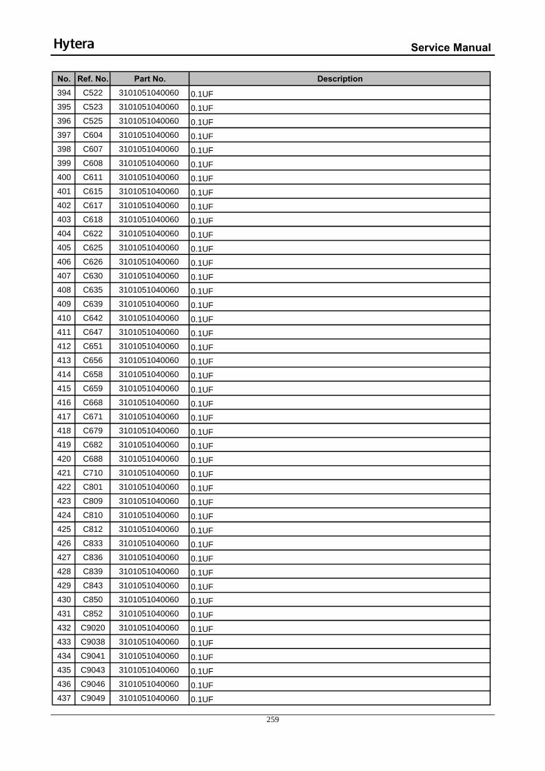
Service Manual
259
No. Ref. No. Part No. Description394 C522 3101051040060 0.1UF395 C523 3101051040060 0.1UF396 C525 3101051040060 0.1UF397 C604 3101051040060 0.1UF398 C607 3101051040060 0.1UF399 C608 3101051040060 0.1UF400 C611 3101051040060 0.1UF401 C615 3101051040060 0.1UF402 C617 3101051040060 0.1UF403 C618 3101051040060 0.1UF404 C622 3101051040060 0.1UF405 C625 3101051040060 0.1UF406 C626 3101051040060 0.1UF407 C630 3101051040060 0.1UF408 C635 3101051040060 0.1UF409 C639 3101051040060 0.1UF410 C642 3101051040060 0.1UF411 C647 3101051040060 0.1UF412 C651 3101051040060 0.1UF413 C656 3101051040060 0.1UF414 C658 3101051040060 0.1UF415 C659 3101051040060 0.1UF416 C668 3101051040060 0.1UF417 C671 3101051040060 0.1UF418 C679 3101051040060 0.1UF419 C682 3101051040060 0.1UF420 C688 3101051040060 0.1UF421 C710 3101051040060 0.1UF422 C801 3101051040060 0.1UF423 C809 3101051040060 0.1UF424 C810 3101051040060 0.1UF425 C812 3101051040060 0.1UF426 C833 3101051040060 0.1UF427 C836 3101051040060 0.1UF428 C839 3101051040060 0.1UF429 C843 3101051040060 0.1UF430 C850 3101051040060 0.1UF431 C852 3101051040060 0.1UF432 C9020 3101051040060 0.1UF433 C9038 3101051040060 0.1UF434 C9041 3101051040060 0.1UF435 C9043 3101051040060 0.1UF436 C9046 3101051040060 0.1UF437 C9049 3101051040060 0.1UF

Service Manual
260
No. Ref. No. Part No. Description438 C9057 3101051040060 0.1UF439 C9071 3101051040060 0.1UF440 C9082 3101051040060 0.1UF441 C9086 3101051040060 0.1UF442 C9091 3101051040060 0.1UF443 C9092 3101051040060 0.1UF444 C9097 3101051040060 0.1UF445 C9104 3101051040060 0.1UF446 C9120 3101051040060 0.1UF447 C9127 3101051040060 0.1UF448 C154 3101051050160 1uF449 C236 3101051050160 1uF450 C312 3101051050160 1uF451 C314 3101051050160 1uF452 C323 3101051050160 1uF453 C423 3101051050160 1uF454 C515 3101051050160 1uF455 C526 3101051050160 1uF456 C706 3101051050160 1uF457 C707 3101051050160 1uF458 C711 3101051050160 1uF459 C712 3101051050160 1uF460 C831 3101051050160 1uF461 C832 3101051050160 1uF462 C834 3101051050160 1uF463 C840 3101051050160 1uF464 C847 3101051050160 1uF465 C9095 3101051050160 1uF466 C9100 3101051050160 1uF467 C131 3101051200020 12PF468 C274 3101051200020 12PF469 C420 3101051200020 12PF470 C9028 3101051200020 12PF471 C9083 3101051200020 12PF472 C9115 3101051200020 12PF473 C514 3101051210000 120PF474 C521 3101051210000 120PF475 C9088 3101051210000 120PF476 C127 3101051500020 15PF477 C9105 3101051500020 15PF478 C9130 3101051500020 15PF479 C190 3101051510000 150PF480 C275 3101051520000 1500PF481 C276 3101051520000 1500PF

Service Manual
261
No. Ref. No. Part No. Description482 C277 3101051520000 1500PF483 C289 3101051520000 1500PF484 C304 3101051520000 1500PF485 C9065 3101051520000 1500PF486 C516 3101051590000 1.5PF487 C518 3101051590000 1.5PF488 C109 3101051800010 18PF489 C194 3101051800010 18PF490 C517 3101051800010 18PF491 C9029 3101051800010 18PF492 C9056 3101051800010 18PF493 C9077 3101051800010 18PF494 C9079 3101051800010 18PF495 C9099 3101051800010 18PF496 C9107 3101051800010 18PF497 C9111 3101051800010 18PF498 C203 3101052000020 20PF499 C204 3101052000020 20PF500 C432 3101052000020 20PF501 C644 3101052000020 20PF502 C672 3101052000020 20PF503 C9087 3101052000020 20PF504 C9101 3101052000020 20PF505 C9058 3101052200010 22PF506 C9112 3101052200010 22PF507 C9129 3101052200010 22PF508 C132 3101052210010 220PF509 C427 3101052210010 220PF510 C645 3101052210010 220PF511 C674 3101052210010 220PF512 C708 3101052210020 220PF513 C160 3101052220010 2200pF514 C431 3101052220010 2200pF515 C212 3101052240010 0.22UF516 C216 3101052240010 0.22UF517 C217 3101052240010 0.22UF518 C218 3101052240010 0.22UF519 C221 3101052240010 0.22UF520 C222 3101052240010 0.22UF521 C226 3101052240010 0.22UF522 C230 3101052240010 0.22UF523 C234 3101052240010 0.22UF524 C238 3101052240010 0.22UF525 C242 3101052240010 0.22UF

Service Manual
262
No. Ref. No. Part No. Description526 C248 3101052240010 0.22UF527 C249 3101052240010 0.22UF528 C683 3101052240010 0.22UF529 C803 3101052240010 0.22UF530 C821 3101052240010 0.22UF531 C824 3101052240010 0.22UF532 C186 3101052700000 27PF533 C151 3101052710000 270PF534 C175 3101052710000 270PF535 C207 3101052710000 270PF536 C262 3101052710000 270PF537 C270 3101052710000 270PF538 C285 3101052710000 270PF539 C290 3101052710000 270PF540 C291 3101052710000 270PF541 C292 3101052710000 270PF542 C313 3101052710000 270PF543 C315 3101052710000 270PF544 C316 3101052710000 270PF545 C317 3101052710000 270PF546 C321 3101052710000 270PF547 C322 3101052710000 270PF548 C325 3101052710000 270PF549 C326 3101052710000 270PF550 C334 3101052710000 270PF551 C469 3101052710000 270PF552 C470 3101052710000 270PF553 C471 3101052710000 270PF554 C804 3101052710000 270PF555 C119 3101053300000 33PF556 C189 3101053300000 33PF557 C448 3101053300000 33PF558 C9078 3101053300000 33PF559 C110 3101053310030 330PF560 C176 3101053310030 330PF561 C196 3101053310030 330PF562 C208 3101053310030 330PF563 C9125 3101053900000 39PF564 C209 3101053920000 3900PF565 C213 3101053920000 3900PF566 C219 3101053920000 3900PF567 C227 3101053920000 3900PF568 C231 3101053920000 3900PF569 C233 3101053920000 3900PF

Service Manual
263
No. Ref. No. Part No. Description570 C239 3101053920000 3900PF571 C240 3101053920000 3900PF572 C241 3101053920000 3900PF573 C245 3101053920000 3900PF574 C246 3101053920000 3900PF575 C247 3101053920000 3900PF576 C638 3101053920000 3900PF577 C650 3101053920000 3900PF578 C662 3101053920000 3900PF579 C666 3101053920000 3900PF580 C684 3101053920000 3900PF581 C686 3101053920000 3900PF582 C687 3101053920000 3900PF583 C808 3101053920000 3900PF584 C813 3101053920000 3900PF585 C820 3101053920000 3900PF586 C823 3101053920000 3900PF587 C858 3101053920000 3900PF588 C223 3101054700010 47PF589 C229 3101054700010 47PF590 C271 3101054700010 47PF591 C272 3101054700010 47PF592 C273 3101054700010 47PF593 C279 3101054700010 47PF594 C286 3101054700010 47PF595 C425 3101054700010 47PF596 C9040 3101054700010 47PF597 C9052 3101054700010 47PF598 C9089 3101054700010 47PF599 C9108 3101054700010 47PF600 C101 3101054710010 470PF601 C187 3101054710010 470PF602 C191 3101054710010 470PF603 C214 3101054710010 470PF604 C220 3101054710010 470PF605 C228 3101054710010 470PF606 C232 3101054710010 470PF607 C237 3101054710010 470PF608 C243 3101054710010 470PF609 C244 3101054710010 470PF610 C255 3101054710010 470PF611 C256 3101054710010 470PF612 C257 3101054710010 470PF613 C258 3101054710010 470PF

Service Manual
264
No. Ref. No. Part No. Description614 C259 3101054710010 470PF615 C263 3101054710010 470PF616 C264 3101054710010 470PF617 C266 3101054710010 470PF618 C268 3101054710010 470PF619 C269 3101054710010 470PF620 C278 3101054710010 470PF621 C280 3101054710010 470PF622 C281 3101054710010 470PF623 C282 3101054710010 470PF624 C283 3101054710010 470PF625 C284 3101054710010 470PF626 C287 3101054710010 470PF627 C288 3101054710010 470PF628 C293 3101054710010 470PF629 C294 3101054710010 470PF630 C295 3101054710010 470PF631 C296 3101054710010 470PF632 C297 3101054710010 470PF633 C298 3101054710010 470PF634 C299 3101054710010 470PF635 C300 3101054710010 470PF636 C301 3101054710010 470PF637 C302 3101054710010 470PF638 C303 3101054710010 470PF639 C305 3101054710010 470PF640 C331 3101054710010 470PF641 C332 3101054710010 470PF642 C333 3101054710010 470PF643 C335 3101054710010 470PF644 C336 3101054710010 470PF645 C444 3101054710010 470PF646 C459 3101054710010 470PF647 C512 3101054710010 470PF648 C652 3101054710010 470PF649 C680 3101054710010 470PF650 C681 3101054710010 470PF651 C685 3101054710010 470PF652 C703 3101054710010 470PF653 C704 3101054710010 470PF654 C835 3101054710010 470PF655 C838 3101054710010 470PF656 C842 3101054710010 470PF657 C845 3101054710010 470PF

Service Manual
265
No. Ref. No. Part No. Description658 C846 3101054710010 470PF659 C848 3101054710010 470PF660 C849 3101054710010 470PF661 C851 3101054710010 470PF662 C853 3101054710010 470PF663 C856 3101054710010 470PF664 C857 3101054710010 470PF665 C9048 3101054710010 470PF666 C9069 3101054710010 470PF667 C9081 3101054710010 470PF668 C9117 3101054710010 470PF669 C9063 3101054720000 4700PF670 C9133 3101054790040 4.7PF671 C513 3101055600000 56PF672 C524 3101055600000 56PF673 C9113 3101055600000 56PF674 C9114 3101055600000 56PF675 C9118 3101055600000 56PF676 C9122 3101055600000 56PF677 C260 3101055610000 560PF678 C261 3101055610000 560PF679 C614 3101055690110 5.6PF680 C100 3101058200000 82PF681 C9141 3101058200000 82PF682 C152 3101060200010 2PF683 C122 3101060400010 4PF684 C133 3101060400010 4PF685 C125 3101060500010 5PF686 C144 3101060500010 5PF687 C9027 3101060500010 5PF688 C143 3101060600010 6PF689 C147 3101060600010 6PF690 C452 3101060700020 7PF691 C9004 3101060700020 7PF692 C9005 3101060700020 7PF693 C123 3101060800010 8PF694 C128 3101060800010 8PF695 C9010 3101060800010 8PF696 C9003 3101061000000 10PF697 C9023 3101061000000 10PF698 C9008 3101061010010 100PF699 C9009 3101061010010 100PF700 C9011 3101061010010 100PF701 C9013 3101061020000 1000PF

Service Manual
266
No. Ref. No. Part No. Description702 C9060 3101061020000 1000PF703 C442 3101061030010 0.01UF704 C619 3101061030010 0.01UF705 C605 3101061050060 1UF706 C609 3101061050060 1UF707 C623 3101061050060 1UF708 C648 3101061050060 1UF709 C669 3101061050060 1UF710 C677 3101061050060 1UF711 C701 3101061050060 1UF712 C816 3101061050060 1UF713 C450 3101061230000 0.012UF714 C145 3101061300000 13PF715 C146 3101061300000 13PF716 C149 3101061590010 1.5PF717 C9012 3101061810010 180PF718 C150 3101062200010 22PF719 C9015 3101062200010 22PF720 C9017 3101062200010 22PF721 C9054 3101062200010 22PF722 C210 3101062240000 0.22UF723 C628 3101062240000 0.22UF724 C640 3101062240000 0.22UF725 C655 3101062240000 0.22UF726 C676 3101062240000 0.22UF727 C678 3101062240000 0.22UF728 C140 3101062250000 2.2UF729 C157 3101062250000 2.2UF730 C158 3101062250000 2.2UF731 C467 3101062250000 2.2UF732 C472 3101062250000 2.2UF733 C601 3101062250000 2.2UF734 C606 3101062250000 2.2UF735 C610 3101062250000 2.2UF736 C624 3101062250000 2.2UF737 C641 3101062250000 2.2UF738 C649 3101062250000 2.2UF739 C653 3101062250000 2.2UF740 C660 3101062250000 2.2UF741 C670 3101062250000 2.2UF742 C825 3101062250000 2.2UF743 C828 3101062250000 2.2UF744 C134 3101062400010 24PF745 C153 3101062400010 24PF

Service Manual
267
No. Ref. No. Part No. Description746 C9031 3101062400010 24PF747 C130 3101062700010 27PF748 C9024 3101063000010 30PF749 C455 3101063320000 3300PF750 C456 3101063690000 3.6PF751 C443 3101063900000 39PF752 C458 3101063900000 39PF753 C460 3101064700000 47PF754 C9021 3101064700000 47PF755 C324 3101064710000 470PF756 C129 3101064790010 4.7PF757 C148 3101065600000 56PF758 C437 3101065620010 5600PF759 C461 3101068200000 82PF760 C802 3101071060010 10UF761 C177 3101072240000 0.22UF762 C463 3101072240000 0.22UF763 C178 3101073340000 0.33UF764 C603 3101074750000 4.7UF765 C621 3101074750000 4.7UF766 C629 3101074750000 4.7UF767 C185 3104072250060 2.2UF768 C468 3104076840020 0.68UF769 C9051 3104082260060 22UF770 C646 3110061050000 1uF771 C657 3110061050000 1uF772 C667 3110061050000 1uF773 C636 3110071060000 10uF774 C661 3110071060000 10uF775 C627 3110081060000 10uF776 C654 3110081060000 10uF777 C637 3110994760000 47uF778 C665 3110994760000 47uF779 C519 3199050758000 0.75PF780 L9030 3210106121000 120nH781 L9017 3210106360000 36nH782 L506 3210106390000 39nH783 L127 3210106820000 82nH784 L9011 3210209102010 1uH785 L507 3210305180000 18nH786 L125 3210305330000 33nH787 L508 3210305829000 8.2nH788 L509 3210305829000 8.2nH789 L9026 3210306151000 150nH
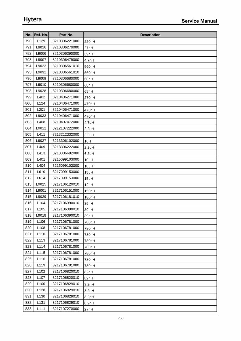
Service Manual
268
No. Ref. No. Part No. Description790 L129 3210306221000 220nH791 L9016 3210306270000 27nH792 L9006 3210306390000 39nH793 L9007 3210306479000 4.7nH794 L9022 3210306561010 560nH795 L9032 3210306561010 560nH796 L9009 3210306680000 68nH797 L9010 3210306680000 68nH798 L9028 3210306680000 68nH799 L402 3210406271000 270nH800 L124 3210406471000 470nH801 L201 3210406471000 470nH802 L9033 3210406471000 470nH803 L408 3210407472000 4.7uH804 L9012 3212107222000 2.2uH805 L411 3213212332000 3.3uH806 L9027 3213306102000 1uH807 L409 3213306222000 2.2uH808 L413 3213306682000 6.8uH809 L401 3215099103000 10uH810 L404 3215099103000 10uH811 L610 3217099153000 15uH812 L614 3217099153000 15uH813 L9025 3217106120010 12nH814 L9001 3217106151000 150nH815 L9029 3217106181010 180nH816 L104 3217106390010 39nH817 L105 3217106390010 39nH818 L9018 3217106390010 39nH819 L106 3217106781000 780nH820 L108 3217106781000 780nH821 L110 3217106781000 780nH822 L113 3217106781000 780nH823 L114 3217106781000 780nH824 L115 3217106781000 780nH825 L116 3217106781000 780nH826 L119 3217106781000 780nH827 L102 3217106820010 82nH828 L107 3217106820010 82nH829 L100 3217106829010 8.2nH830 L128 3217106829010 8.2nH831 L130 3217106829010 8.2nH832 L131 3217106829010 8.2nH833 L111 3217107270000 27nH

Service Manual
269
No. Ref. No. Part No. Description834 L112 3217107470000 47nH835 L118 3217107470000 47nH836 L117 3217107680010 68nH837 L109 3221505121010 Bead
838 L120 3221505121010 Bead
839 L121 3221505121010 Bead
840 L122 3221505121010 Bead
841 L123 3221505121010 Bead
842 L133 3221505121010 Bead
843 L301 3221505121010 Bead
844 L403 3221505121010 Bead
845 L405 3221505121010 Bead
846 L407 3221505121010 Bead
847 L412 3221505121010 Bead
848 L702 3221505121010 Bead
849 L801 3221505121010 Bead
850 L803 3221505121010 Bead
851 L804 3221505121010 Bead
852 L805 3221505121010 Bead
853 L821 3221505121010 Bead
854 L822 3221505121010 Bead
855 L9020 3221505121010 Bead
856 R712 3221505121010 Bead
857 L9014 3221506121000 Bead
858 L303 3221506181000 Bead
859 L601 3221506181000 Bead
860 L602 3221506181000 Bead
861 L603 3221506181000 Bead
862 L605 3221506181000 Bead
863 L606 3221506181000 Bead
864 L609 3221506181000 Bead
865 L611 3221506181000 Bead
866 L612 3221506181000 Bead
867 L617 3221506181000 Bead
868 L802 3221506181000 Bead
869 R614 3221506181000 Bead
870 R622 3221506181000 Bead
871 L302 3221506601000 Bead
872 L304 3221506601000 Bead
873 L305 3221506601000 Bead
874 L410 3221506601000 Bead
875 L820 3221506601000 Bead
876 L823 3221506601000 Bead
877 L827 3221506601000 Bead

Service Manual
270
No. Ref. No. Part No. Description878 L828 3221506601000 Bead
879 L502 3221506601080 Bead
880 L505 3221506601080 Bead
881 L9019 3231301030000 Air-core coil
882 L9023 3233099100000 Air-core coil
883 L9021 3233099185900 Air-core coil
884 L9003 3233099330000 Air-core coil
885 L9005 3233099330000 Air-core coil
886 L9004 3233099400000 Air-core coil
887 R9004 3233099449000 Air-core coil
888 L9008 3233099470000 Air-core coil
889 L9013 3233099470000 Air-core coil
890 L816 3237199270000 Air-core coil
891 L9015 3237199270000 Air-core coil
892 L9024 3237199270000 Air-core coil
893 L9035 3237199270000 Air-core coil
894 L607 3290299222000 2.2uH895 L613 3290299222000 2.2uH896 L615 3290299222000 2.2uH897 L616 3290299222000 2.2uH898 L501 3297106339000 3.3nH899 L503 3297106339000 3.3nH900 L504 3297106339000 3.3nH901 L406 3297107391000 390nH902 D9017 3301250300000 Schottky barrier diode903 D604 3303030100010 Switching diode904 D9011 3303030100010 Switching diode905 D9002 3303030800040 Switching diode906 D302 3303990000010 Switching diode907 D104 3303990000060 Switching diode908 D105 3303990000060 Switching diode909 D112 3303990000060 Switching diode910 D113 3303990000060 Switching diode911 D114 3303990000060 Switching diode912 D115 3303990000060 Switching diode913 D116 3303990000060 Switching diode914 D9003 3303990000060 Switching diode915 D9004 3303990000060 Switching diode916 D9007 3303990000060 Switching diode917 D9008 3303990000060 Switching diode918 D101 3304010100180 Varactor
919 D109 3304010100180 Varactor
920 D402 3304010100220 Varactor
921 D111 3304010100890 Varactor

Service Manual
271
No. Ref. No. Part No. Description922 D102 3304010100990 Varactor
923 D107 3304010100990 Varactor
924 D108 3304010100990 Varactor
925 D110 3304010100990 Varactor
926 D103 3304010400000 Varactor
927 D106 3304010400000 Varactor
928 D9005 3304060300040 Varactor
929 D9009 3304060300040 Varactor
930 D9012 3304060300040 Varactor
931 D9013 3304060300040 Varactor
932 D401 3304060300050 Varactor
933 D301 3307110100060 LED934 D303 3310040000000 LED
935 D304 3310040000000 ESD protection diode
936 D305 3310040000000 ESD protection diode
937 D306 3310040000000 ESD protection diode
938 D318 3399040600010 ESD protection diode
939 D307 3399040600020 ESD protection diode
940 D308 3399040600020 ESD protection diode
941 D309 3399040600020 ESD protection diode
942 D310 3399040600020 ESD protection diode
943 D602 3399040600020 ESD protection diode
944 D9010 3399990000080 ESD protection diode
945 D601 3399990000110 Diode946 D9006 3399990000260 Switching diode947 Q9021 3401001000490 PNP transistor
948 Q105 3403003000060 NPN transistor
949 Q401 3403003000060 NPN transistor
950 Q312 3403008000010 BRT
951 Q801 3403008000010 BRT
952 Q802 3403008000010 BRT
953 Q9007 3403008000010 BRT
954 Q9008 3403008000010 BRT
955 Q9001 3403014000020 Compound transistor
956 Q103 3403999000000 Compound transistor
957 Q106 3403999000000 Compound transistor
958 Q107 3403999000000 Compound transistor
959 Q9019 3403999000000 Compound transistor
960 Q9020 3403999000000 Compound transistor
961 Q9017 3404006000000 NPN transistor
962 Q9018 3404006000000 NPN transistor
963 Q9004 3406001000090 NPN transistor
964 Q102 3408002000000 NPN transistor
965 Q403 3408002000000 NPN transistor

Service Manual
272
No. Ref. No. Part No. Description966 Q9002 3408002000000 NPN transistor
967 Q104 3408002000080 NPN transistor
968 Q108 3408002000080 NPN transistor
969 Q9006 3410001000020 PNP transistor
970 Q603 3414001000040 NPN transistor
971 Q9009 3418001000010 NPN transistor
972 Q402 3499000000150 Compound transistor
973 Q604 3503020000030 N-MOSFET
974 Q607 3503020000030 N-MOSFET
975 Q9005 3504990000010 MOSFET976 Q9003 3504990000040 MOSFET977 Q605 3505010000059 P-MOSFET
978 Q310 3511990000010 N-MOSFET
979 Q313 3511990000010 N-MOSFET
980 U801 3602023005740 Audio amplifier
981 U401 3603999000000 IF processor
982 U103 3604019000000 PLL983 U102 3605002057290 Operational amplifier984 U9002 3605025000020 Operational amplifier985 U701 3606010000010 D/A converter986 U603 3608006000000 Power management IC987 U606 3608006000000 Power management IC988 U608 3608006000000 Power management IC989 U609 3608006000000 Power management IC990 U612 3608006000000 Power management IC991 U610 3608006000030 Power management IC992 U601 3608011000050 Power management IC993 U611 3608011000050 Power management IC994 U604 3608020005750 Power management IC995 U605 3608020005750 Power management IC996 U105 3609003999000 Mini IC 997 U607 3609010000170 Reset IC998 U501 3609999000300 GPS LNA999 U201 3610010000010 MCU
1000 U244 3612002000020 Memory1001 U242 3612044000010 Memory1002 U821 3613010000000 Baseband processor1003 U820 3616037000020 Switch1004 U101 3616059000000 Switch1005 U104 3616059000000 Switch1006 X101 3701019250030 VC-TCXO
1007 X203 3701019250040 TCXO
1008 X201 3701327610060 Crystal1009 Z9001 3802448540040 Crystal filter

Service Manual
273
No. Ref. No. Part No. Description1010 Z501 3804157560000 GPS filter1011 U312 3805000000030 EMI filter1012 U313 3805000000030 EMI filter1013 U314 3805000000030 EMI filter1014 U315 3805000000030 EMI filter1015 U316 3805000000030 EMI filter1016 U317 3805000000030 EMI filter1017 U318 3805000000030 EMI filter1018 U319 3805000000030 EMI filter1019 U320 3805000000030 EMI filter1020 U321 3805000000030 EMI filter1021 U322 3805000000030 EMI filter1022 F602 4010000000010 Fuse
1023 F601 4099000000050 Fuse1024 J821 5201016000010 Board-to-board connector1025 J311 5201030000040 Board-to-board connector1026 J1601 5201050100030 Board-to-board connector1027 J313 5202002100200 Board-to-board connector1028 J601 5205003100020 Battery connector1029 U9003 5404000000060 Sensor1030 T9001 5406000000200 Transformer1031 T9002 5406000000200 Transformer1032 / 6201809000000 Shielding can for IF processor1033 / 6201810000000 Shielding can for baseband processor 1034 ANT1 6201847000000 Antenna spring plate1035 / 6201859000000 Shielding frame for lowpass filter1036 / 6201860000000 Shielding frame for GPS1037 / 6201862000000 Shielding can for TX VCO1038 / 6201865000000 Shielding can for crystal oscillator1039 / 6201915000000 Shielding can for antenna spring plate 1040 / 6201935000000 Shielding can for switching power1041 41PD7001002A0 Main board

Service Manual
274
Channel Board for PD70X/ PD70XG/ HD705/ HD705G No. Ref. No. Part No. Description1 R1002 3001051210010 120Ω
2 C1001 3101052710000 270PF
3 C1002 3101052710000 270PF
4 C1003 3101052710000 270PF
5 C1004 3101052710000 270PF
6 C1005 3101052710000 270PF
7 C1006 3101052710000 270PF
8 C1007 3101052710000 270PF
9 C1010 3101052710000 270PF
10 C1011 3101052710000 270PF
11 C1012 3101052710000 270PF
12 D1001 3310040000000 ESD protection diode
13 D1003 3310040000000 ESD protection diode
14 D1004 3310040000000 ESD protection diode
15 D1005 3310040000000 ESD protection diode
16 D1006 3310040000000 ESD protection diode
17 D1007 3310040000000 ESD protection diode
18 D1008 3310040000000 ESD protection diode
19 D1011 3310040000000 ESD protection diode
20 D1014 3310040000000 ESD protection diode
21 D1009 3399040600020 ESD protection diode
22 D1013 3399040600020 ESD protection diode
23 D1002 3307120100050 LED
24 Q1001 3403009000010 Compound transistor
25 U1001 3805000000040 EMI filter
26 J1001 5201016100040 Board-to-board connector
27 S1003 4301080000020 Momentary contact switch
28 41PD7002002B0 PCB
29 R1001 3001056810000 680Ω
30 C1015 3101051040060 0.1UF
31 C1016 3101051040060 0.1UF
32 C1017 3101051040060 0.1UF
33 L1001 3221506181000 Bead
34 U1002 3608006000030 Power management IC

Service Manual
275
Channel Board for PD78X/ PD78XG/ HD785/ HD785G No. Ref. No. Part No. Description1 R1002 3001051210010 120Ω
2 C1001 3101052710000 270PF
3 C1002 3101052710000 270PF
4 C1003 3101052710000 270PF
5 C1004 3101052710000 270PF
6 C1005 3101052710000 270PF
7 C1006 3101052710000 270PF
8 C1007 3101052710000 270PF
9 C1010 3101052710000 270PF
10 C1011 3101052710000 270PF
11 C1012 3101052710000 270PF
12 D1001 3310040000000 ESD protection diode
13 D1003 3310040000000 ESD protection diode
14 D1004 3310040000000 ESD protection diode
15 D1005 3310040000000 ESD protection diode
16 D1006 3310040000000 ESD protection diode
17 D1007 3310040000000 ESD protection diode
18 D1008 3310040000000 ESD protection diode
19 D1011 3310040000000 ESD protection diode
20 D1014 3310040000000 ESD protection diode
21 D1009 3399040600020 ESD protection diode
22 D1013 3399040600020 ESD protection diode
23 D1002 3307120100050 LED
24 Q1001 3403009000010 Compound transistor
25 U1001 3805000000040 EMI filter
26 J1001 5201016100040 Board-to-board connector
27 S1003 4301080000020 Momentary contact switch
28 41PD7802006C0 PCB
29 R1001 3001056810000 680Ω
30 C1015 3101051040060 0.1UF
31 C1016 3101051040060 0.1UF
32 C1017 3101051040060 0.1UF
33 L1001 3221506181000 Bead
34 U1002 3608006000030 Power management IC

Service Manual
276
Keyboard for PD78X/ PD78XG/ HD785/ HD785G No. Ref. No. Part No. Description1 R1 3001051010000 100Ω
2 R2 3001051010000 100Ω
3 R3 3001051010000 100Ω
4 R4 3001051010000 100Ω
5 R5 3001051010000 100Ω
6 R6 3001051010000 100Ω
7 R7 3001051010000 100Ω
8 D1 3307990000260 LED
9 D2 3307990000260 LED
10 D3 3307990000260 LED
11 D4 3307990000260 LED
12 D5 3307990000260 LED
13 D6 3307990000260 LED
14 D7 3307990000260 LED
15 D8 3310040000010 ESD protection diode
16 D9 3310040000010 ESD protection diode
17 J4 5201016000010 Board-to-board connector

Service Manual
277
13.8 Troubleshooting Flow Chart Receiver Circuit

Service Manual
278
Description of Normal Situations: [1] Output voltage by Q9019 PIN3: about 4.95V. [2] Output voltage by U605 PIN4 or input voltage into Q9019 PIN4: about 5V. [3] Vbe: about 0.74V; Vce: about 2.5V (in the case of no signal reception). [4] For Q9018, Vbe: about 0.76V; Vce: about 0.95V; for Q9017, Vbe: about 0.7V; Vce:0.85V (in the case of no signal reception). [5] Cut off the front-end circuit, and input a 44.85MHz IF signal at TP402 to test IF sensitivity. Normally, the IF sensitivity is -109dBm. [6] Frequency of Q403: 47.1/42.6MHz. [7] Frequency of L411: 18MHz. [8] Input -30dBm RF signal at the antenna connector and test at TP9004. Normally, gain>10dB, output signal>-20dBm. [9] Input -30dBm RF signal at the antenna connector and test at R9005 (do not cut off the back-end circuit). Normally, gain>1dB, output signal>-29dBm. [10] Signal frequency: RF-IF, signal amplitude>2dBm. [11] For input of -80dBm signal at L9022, gain>25dB, output signal>-55dBm; for input of -30dBm signal, output signal<-20dBm. [12] The input signal at the antenna connector, with standard tuning information (AF=1KHz, FM=3KHz), is -47dBm.

Service Manual
279
Transmitter Circuit
No power output
Power supply works normally?[1]
Check the power supply circuit.
No
APC-OUT is normal?[2]
TX 5V voltageis normal?[5]
APC-IN is normal?[3]
Yes
No
PS-APC 3.3V is normal?[4]
Yes
PS-TX and RT5V are normal?[5]
No
Yes
No
Match circuit is normal?[8]
Yes
Yes
No
Q9003 works normally?[9]
Yes
Repair damaged components.
Power is normal? CompletedYesNo
No Replace Q9003 and bias resistor.
Power is normal? CompletedYes
Q9005 works normally?[10]
D9002,spring plate for antenna and the low-pass
filter are normal?[7]
Repair damaged components.
Yes
No
Power is normal? CompletedYesNo
NoYes
Replace Q9005 and bias resistor.
Q9004 works normally?[11]
Power is normal? CompletedYesNoYes
No
Replace Q9004 and bias resistor.
Power is normal? CompletedYesNo
No
Q9002/D9007 works normally?[12]
Replace Q9002 and bias resistor.
Power is normal? CompletedYesNo
Check the output circuit of FGU.
No
Yes
Replace Q9020 and U9002.
Power is normal?[6] Completed
YesNo
Yes
Check the DAC output circuit.
Yes Replace Q9008 and Q9006.
Check the power supply circuit.
No
No

Service Manual
280
Description of Normal Situations: [1] Voltage of the power supply: about 7.4V. [2] For low power, APC-OUT: 1.8-2.1V; for high power, APC-OUT: 2.4-2.8V. [3] For low power, APC-IN: 1-1.3V; for high power, APC-IN: 1.8-2.1V. [4] PS-APC: about 3.3V. [5] TX5V: about 5V; RT5V: about 5V; PS-TX: about 3.3V. High power: about 4.7W; low power: about 1.2W. [7] Start-up voltage of D9002: about 0.7V. The low-pass filter must be soldered appropriately and remain in good condition. The spring plate for the antenna must be well fitted into the antenna connector. [8] The match components must not be soldered inappropriately or damaged. [9] Vdd: about 7.3V; for low power, Vgg: 1-1.2V; for high power, Vgg: 1.35-1.55V. [10] Vdd: about 7.3V; for low power, Vgg: 1.8-2.1V; for high power, Vgg: 2.4-2.8V. [11] Vc: about 4.8V; Vb: about 1.4V; Ve: about 1.1V. [12] Vc: about 4.7V; Vb: about 0.7V; Ve: 0V. Start-up voltage of D9007: about 0.7V. Note: The above check operations should be made under 7.4V voltage.

Service Manual
281
FGU
FGU check
Check the power supply circuit.5VFGU, 3V3ARF,
3V3DRF are normal?
VCO oscillates?
Q106 、Q110输出是否正常?
反馈是
否正常?
Yes
Yes
Yes
CV voltage is normal?[3]
Feedback is output?
Yes
Yes
Yes
No
Replace Q106 and Q107.
Q106 and Q107 are normal?[1]
Q104 and Q108 are normal?[2]
No
No
YesReplace Q104
and Q108.
No
Check Q104, Q108 and peripheral components.
Yes
NoL110 and L116 are
normal?[4]Replace L110 and
L116.
No
Q101 and Q102 are normal?[5]
Check the feedback circuit.
No
19.2MHz crystal oscillates?
Check the 19.2MHz circuit.
No
Sky72310 clock is normal?[6]
CompletedYes
Check the data circuit of the
control circuit.
No
Check Q101, Q102 and peripheral components.
Replace Q101 and Q102.
No
Yes

Service Manual
282
Description of Normal Situations: [1] During transmission, output voltage by Q107 PIN3: about 4V. During reception, output voltage by Q106 PIN3: about 4V. [2] During transmission, voltage at Q108 E: about 1.8V. During reception, voltage at Q104 E: about 1.8V. [3] The CV value varies with frequencies. Generally, it is within the range 0.5V-4.5V. [4] L110/L116 is on. [5] Voltage at Q101/Q102 B: about 0.7V. [6] MCSI-CLK-PLL outputs 960KHz clock.

Service Manual
283
14. Disassembly and Assembly
Note: The disassembly and assembly operations for PD70X/ PD70XG/ HD705/ HD705G and PD78X/
PD78XG/ HD785/ HD785G are similar. This section illustrates based on PD78X/ PD78XG/ HD785/
HD785G.
Disassembling the Chassis 1. Turn off the radio, and remove the two screws on the sides of the radio. 2. Remove the two screws on the bottom of the chassis. 3. Remove the Radio On-Off/Volume Control knob and Channel Selector knob.
4. Push the chassis upwards, and take the 50-pin connector down (see the arrow in the figure below).
Then you can take the chassis out.
Disassembling the TX and RX Units 1. Remove the screws on the PTT board. 2. Remove the screws on the LCD board (for PD70X/ PD70XG/ HD705/ HD705G, please remove the
screws on the small board). 3. Remove the screws on the main board. 4. Take the main board down the chassis.

Service Manual
284
Precautions for Assembly
1. Make sure the waterproof ring surrounding the chassis is well fitted into the slot.
2. Insert the chassis into the radio case.
3. Attach the 50-pin board-to-board connector.
4. Press the bottom of the chassis downwards to fit the chassis into the radio case.

Service Manual
285
15. Exploded View
PD70X/ PD70XG/ HD705/ HD705G

Service Manual
286
No. Part No. Description Qty.1 6001277000000 Accessory jack cover (RoHS) 1 2 6001073000000 Light guide (RoHS) 1 3 6001069000010 Volume control knob (RoHS) 1 4 16010435H0010 Stubby antenna (RoHS) 1 5 6001068000010 Channel selector knob (RoHS) 1 6 6100502000000 Emergency key (RoHS) 1 7 7209002501000 Nut for antenna (RoHS) 1 8 7206002500200 Nut for volume switch (RoHS) 1 9 Channel board (RoHS) 1
10 7207002201000 Nut for encoder switch (RoHS) 1 11 7000218000000 Stud (RoHS) 2 12 1300PD7000090 FPC (RoHS) 1 13 7102003500210 Machine screw (RoHS) 11 14 Semi-finished main board (RoHS) 1 15 6201848000000 Motor fixing sheet (RoHS) 1 16 5402000000060 Motor connector (RoHS) 1 17 4400000048000 SMA RF connector (RoHS) 1 18 6001070000000 Rear cover (RoHS) 1 19 6100505000000 Waterproof ring for battery connector (RoHS) 1 20 6100503000000 Waterproof ring for radio (RoHS) 1 21 6100527100000 Waterproof ring for machine screw (RoHS) 4 22 7102009000020 Machine screw (RoHS) 2 23 7101904020300 Self-tapping screw (RoHS) 2 24 6300116001000 Aluminum chassis (RoHS) 1 25 6100111000010 Silicone rubber MIC cover (RoHS) 1 26 6201870000000 Speaker fixing sheet (RoHS) 1 27 5001210000400 Speaker (RoHS) 1 28 6000787000000 PTT key cover (RoHS) 1 29 6100442000000 Silicone rubber PTT key (RoHS) 1 30 7102004000400 Machine screw (RoHS) 2 31 7400264000000 Speaker felt (RoHS) 1 32 6001063000010 Front case (RoHS) 1
Note: Parts that are not marked with Part No. may vary with the radio frequency band.

Service Manual
287
PD78X/ PD78XG/ HD785/ HD785G

Service Manual
288
No. Part No. Description Qty.1 7400320000020 LCD lens (RoHS) 1 2 6001071000000 Front cover (RoHS) 1 3 6100441000000 Numeric keypad (RoHS) 1 4 7300044000010 Metal dome for function key 00 (RoHS) 1 5 6001277000000 Accessory jack cover (RoHS) 1 6 6001065000010 Front case (RoHS) 1 7 6001073000000 Light guide (RoHS) 1 8 6001069000010 Volume control knob (RoHS) 1 9 16010435H0010 Stubby antenna (RoHS) 1
10 6001068000010 Channel selector knob (RoHS) 1 11 6100502000000 Emergency key (RoHS) 1 12 7400184000000 Waterproof MIC net (RoHS) 1 13 7400329000000 MIC pad (RoHS) 1 14 7500346000000 PORON (RoHS) 1 15 7206002500200 Nut for volume switch (RoHS) 1 16 6100111000010 Silicone rubber MIC cover (RoHS) 1 17 7207002201000 Nut for encoder switch (RoHS) 1 18 7209002501000 Nut for antenna (RoHS) 1 19 4400000048000 SMA RF connector (RoHS) 1 20 6300116001000 Aluminum chassis (RoHS) 1 21 6100503000000 Waterproof ring for radio (RoHS) 1 22 6100505000000 Waterproof ring for battery connector (RoHS) 1 23 6001070000000 Rear cover (RoHS) 1 24 7000238000000 Pad (RoHS) 1 25 7102004000400 Machine screw (RoHS) 2 26 5001210000400 Speaker (RoHS) 1 27 7101904020300 Self-tapping screw (RoHS) 2 28 6100442000000 Silicone rubber PTT key (RoHS) 1 29 6201870000000 Speaker fixing sheet (RoHS) 1 30 6000787000000 PTT key cover (RoHS) 1 31 1300PD7800000 50PIN B2B connector (RoHS) 1 32 7102003500210 Machine screw (RoHS) 11 33 Semi-finished channel board (RoHS) 1 34 7000218000000 Stud (RoHS) 2 35 Semi-finished main board (RoHS) 1 36 6100527100000 Waterproof ring for machine screw (RoHS) 4 37 7102009000020 Machine screw (RoHS) 2 38 7400296000010 Speaker felt (RoHS) 1
Note: Parts that are not marked with Part No. may vary with the radio frequency band.

Service Manual
289
16. Packing Guide Note: This section takes PD78X/ PD78XG/ HD785/ HD785G for example.

Service Manual
290
17. Specifications General
Frequency Range
UHF1: 400-470MHz UHF2: 450-520MHz UHF3: 350-400MHz VHF: 136-174MHz
Channel Capacity PD70X/ PD70XG/ HD705/ HD705G: 32
PD78X/ PD78XG/ HD785/ HD785G: 1024
Channel Spacing 25/20/12.5KHz
Operating Voltage 7.4V (rated)
Battery 2000mAh Li-Ion battery
Battery Life (5-5-90 Duty Cycle, High TX Power)
High-capacity 2000mAh Li-Ion Battery
PD70X/ HD705/ PD78X/ HD785:
Analog: 12.5 hours (UHF); 11 hours (VHF)
Digital: 14.5 hours (UHF); 13.5 hours (VHF)
PD70XG/ HD705G/ PD78XG/ HD785G:
Analog: 11 hours (UHF); 10 hours (VHF)
Digital: 12.5 hours (UHF); 12 hours (VHF)
Operating Temperature -30 ~ +60
Dimensions (H×W×D)
(with standard battery, without
antenna)
PD70X/ PD70XG/ HD705/ HD705G: 125×55×35 mm/ 4.921×2.165×1.378 inch PD78X/ PD78XG/ HD785/ HD785G: 125×55×37 mm/ 4.921×2.165×1.458 inch
Weight (with antenna & standard
battery)
PD70X/ PD70XG/ HD705/ HD705G: 335g/ 0.74lb (UHF);
340g/ 0.75lb (VHF)
PD78X/ PD78XG/ HD785/ HD785G: 355g/ 0.78lb (UHF);
360g/ 0.79lb (VHF)
Frequency Stability ±1.5ppm
Receiver
Analog 0.3μV (12dB SINAD) 0.22μV (Typical) (12dB SINAD) 0.4μV (20dB SINAD)
Sensitivity
Digital 0.3μV /BER5%
Adjacent Channel Selectivity TIA-603 ETSI
60dB @ 12.5 kHz / 70dB @ 20&25 kHz 60dB @ 12.5 kHz / 70dB @ 20&25 kHz
Intermodulation TIA-603
70dB @ 12.5/20/25 kHz

Service Manual
291
ETSI 65dB @ 12.5/20/25 kHz
Spurious Response Rejection TIA-603 ETSI
70dB @ 12.5/20/25 kHz 70dB @ 12.5/20/25 kHz
Blocking 84dB
Rated Audio Power Output 0.5W (16Ω load)
Rated Audio Distortion ≤3%
Transmitter
RF Power Output UHF: 4W/1W VHF: 5W/1W
Conducted/Radiated Emission -36dBm<1GHz -30dBm>1GHz
Modulation Limiting ±2.5kHz @ 12.5 kHz ±4.0kHz @ 20 kHz ±5.0kHz @ 25 kHz
FM Noise 40dB @ 12.5 kHz 43dB @ 20KHz 45dB @ 25 kHz
Audio Distortion ≤3%
GPS (open area)
TTFF (Time To First Fix) Cold Start <1 minute
TTFF (Time To First Fix) Hot Start <10 seconds
Horizontal Accuracy <10 meters
All Specifications are tested according to applicable standards, and subject to change without notice due
to continuous development.

Service Manual
292
18. Appendix
Table of Blind Spots
No. UHF1 (400-470MHz) Blind Spot (MHz)
1 403.2
2 422.4
3 441.6
4 460.8
5 414
6 432
7 450
8 468
9 434.7
10 463.275
11 407.4625
12 407.475
13 411.725
14 411.7375
15 416
16 424.5375
17 426.6625
18 428.8
19 430.9375
20 435.2
21 439.4625
22 439.475
23 443.7375
24 448
25 452.2625
26 452.275

Service Manual
293
27 456.525
28 456.5375
29 458.6625
30 465.0625
31 465.075
Note: Blind spots 11-31 are for R1.0 radios.
No. UHF2 (450-520MHz) Blind Spot (MHz)
1 450
2 468
3 486
4 504
5 480
6 460.8
7 518.4
8 499.2
No. UHF3 (350-400MHz) Blind Spot (MHz)
1 384
2 366.6
3 353.8
4 369.8
5 385.8
6 393.675

Service Manual
294
No. VHF (136-174MHz) Blind Spot (MHz)
1 144
2 140.7
3 162
4 153.6

2011-6-13F03152
1616300000030
is the trademark or registered trademark of Hytera Communications Corp., Ltd. 2011 Hytera Corp., Ltd. All Rights Reserved.
Address: HYT Tower, Hi-Tech Industrial Park North, Beihuan RD., Nanshan District, Shenzhen, ChinaPostcode: 518057
http://www.hytera.com
是海能达通信股份有限公司的商标或注册商标2011 Hytera Corp., Ltd.版权所有
地址:深圳市高新技术产业园北区北环路好易通大厦邮编:518057服务热线 400-830-7020http: www.hytera.com
://