session 7 overview: non-volatile memory solutions
TRANSCRIPT

126 • 2015 IEEE International Solid-State Circuits Conference 978-1-4799-6224-2/15/$31.00 ©2015 IEEE
ISSCC 2015 / SESSION 7 / NON-VOLATILE MEMORY SOLUTIONS / OVERVIEW
Session 7 Overview: Non-Volatile Memory SolutionsMEMORY SUBCOMMITTEE
7.1 A Low-Power 64Gb MLC NAND-Flash Memory in 15nm CMOS Technology 8:30 AMM. Sako, Toshiba Semiconductor and Storage Products, Yokohama, Japan
In Paper 7.1, Toshiba presents a 64Gb MLC NAND Flash memory developed in 15nm CMOS technology. 30MB/s programthroughput and 533Mb/s data transfer rate are achieved even at 1.8V VCC by an optimized datapath design. New designfeatures are introduced to reduce current peak and BL discharging time.
7.2 A 128Gb 3b/cell V-NAND Flash Memory with 1Gb/s I/O Rate 9:00 AMJ-W. Im, Samsung Electronics, Hwaseong, Korea
In Paper 7.2, Samsung presents world’s first 128Gb TLC vertical NAND (V-NAND) Flash memory with 32 stacked WL layers. High-speed program (HSP) and data pre-processing technique enable tPROG of 700μs and endurance over 5K program/erase cycles. 1Gb/s I/O rate is realized by the proposed multiple circuit techniques.
7.3 A 28nm Embedded SG-MONOS Flash Macro for Automotive Achieving 200MHz Read 9:30 AMOperation and 2.0MB/s Write Throughput at Tj of 170°C
Y. Taito, Renesas Electronics, Itami, Japan
In Paper 7.3, Renesas Electronics presents 28nm embedded SG-MONOS Flash macros for automotive uses. 200MHz random read and 2MB/s write throughput at Tj = 170°C with sufficient TDDB lifetime and suppressed RF noise are achievedby introducing 4 circuit techniques.
Strong demand for high-density low-power and reliable non-volatile Memory (NVM) Solutions continues to enable data centers, advanced automotive control, and wearables. In ISSCC 2015, a new 64Gb MLC Flash in 15nm CMOS technology is optimized for low power. Another 128GbV-NAND with 3b/cell is introduced at 1Gb/s I/O rate. A high-speed 28nm embedded SG-MONOS Flash technology is developed for automotiveindustry. Aside from memory technology, system level innovations are critical to achieve high-speed reliable NVM solutions. A frequency-boostinginterface chip is shown to stack 16-die 128Gb Flash at 1GB/s interface. An SSD controller is implemented for high-speed and reliable enterprise-level SSD with TLC Flash. As SRAM and DRAM scaling faces serious challenges, high-speed emerging memories needed to continue area andcost reduction. Two Mb level STTRAM macro papers are shown to achieve sub-10ns read speed, potentially replacing SRAM and DRAM.
Session Chair: Fatih Hamzaoglu,Intel, Hillsboro, OR
Session Co-Chair: Takashi Kono,Renesas Electronics, Hyogo, Japan

127DIGEST OF TECHNICAL PAPERS •
ISSCC 2015 / February 24, 2015 / 8:30 AM
7.4 A Covalent-Bonded Cross-Coupled Current-Mode Sense Amplifier for STT-MRAM 10:15 AMwith 1T1MTJ Common Source-Line Structure ArrayC. Kim, Samsung Electronics, Hwaseong, Korea
In Paper 7.4, Samsung presents a sensing scheme for 8Mb STT-MRAM Macro to achieve 9ns sense speed with 200%TMR and 4% MTJ resistance sigma. Adjacent bitcells share the source line, and reference cell pairs are shared among 128data columns for high density. Less than 2μA can be sensed at 1.5V periphery voltage.
7.5 A 3.3ns-Access-Time 71.2μW/MHz 1Mb Embedded STT-MRAM Using Physically 10:45 AMEliminated Read-Disturb Scheme and Normally-Off Memory ArchitectureH. Noguchi, Toshiba, Kawasaki, Japan
In Paper 7.5, Toshiba presents design techniques to optimize STTRAM array active and idle power, as well as read-disturbreduction. Equalized and hierarchical bitline is shown to reduce bitcell disturb, and multi-level dynamic periphery powerdown is implemented on 1Mb Macro to achieve 72μJ/MHz read and 166μJ/MHz write power with 3.5ns/3ns read/writetime in 2T2MTJ fashion.
7.6 1GB/s 2Tb NAND Flash Multi-Chip Package with Frequency-Boosting Interface Chip 11:15 AMH-J. Kim, Samsung Electronics, Hwaseong, Korea
In Paper 7.6, Samsung presents a frequency boosting interface chip (F-Chip) to alleviate SSD interface speed bottleneck.2Tb NAND Flash MCP with 1GB/s toggle DDR interface is accomplished by incorporating the proposed F-Chip into theNAND MCP including a 16-die stacked 128Gb NAND flash.
7.7 Enterprise-Grade 6× Fast Read and 5× Highly Reliable SSD with TLC NAND-Flash 11:45 AMMemory for Big-Data Storage
T. Tokutomi, Chuo University, Tokyo, Japan
In Paper 7.7, Chuo U presents three SSD controller techniques for high speed and reliable enterprise-level SSD. Fast low-density parity-check (LDPC) reduces the read latency of 1Xnm TLC NAND Flash SSD by 83%. Dynamic VTHoptimization and auto data recovery reduce the NAND flash bit-error rate (BER) by 80% and 17%, respectively.
7

128 • 2015 IEEE International Solid-State Circuits Conference
ISSCC 2015 / SESSION 7 / NON-VOLATILE MEMORY SOLUTIONS / 7.1
7.1 A Low-Power 64Gb MLC NAND-Flash Memory in 15nm CMOS Technology
Mario Sako1, Yoshihisa Watanabe1, Takao Nakajima1, Jumpei Sato1, Kazuyoshi Muraoka1, Masaki Fujiu1, Fumihiro Kouno1, Michio Nakagawa1, Masami Masuda1, Koji Kato1, Yuri Terada1, Yuki Shimizu1, Mitsuaki Honma1, Akihiro Imamoto1, Tomoko Araya1, Hayato Konno1, Takuya Okanaga1, Tomofumi Fujimura1, Xiaoqing Wang1, Mai Muramoto1, Masahiro Kamoshida1, Masatoshi Kohno1, Yoshinao Suzuki1, Tomoharu Hashiguchi1, Tsukasa Kobayashi1, Masashi Yamaoka1, Ryuji Yamashita2
1Toshiba Semiconductor and Storage Products, Yokohama, Japan, 2Sandisk, Yokohama, Japan
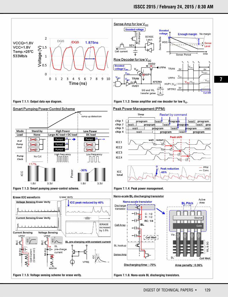
The demand for high-throughput NAND Flash memory systems for mobile applications such as smart phones, tablets, and laptop PCs with solid-state drives (SSDs) has been growing recently. To obtain higher throughput, systemsemploy multiple NAND Flash memories operating simultaneously in parallel. Theavailable power for a mobile device is severely restricted and the peak total operating current may be high enough to cause large supply-voltage drop oreven an unexpected system shutdown. Therefore it is important for NAND Flashmemories to reduce operating power and peak operating current.
To meet these market demands, we develop a low-power 64Gb 2b/cell NANDFlash memory in 15nm CMOS technology. The die can operate at a supply voltage VCC as low as 1.8V without costly additional process enhancements suchas low-Vth transistors. Figure 7.1.7 shows the die micrograph and key features.The die consists of two 32Gb memory planes with 16KB page size and 1k blocks.30MB/s program throughput and 533Mb/s data transfer rate, which are comparable or even higher than the trend [1-3], are achieved even at 1.8V VCC byimplementing a one-sided all-bitline (ABL) architecture [4] and optimized data-path circuitry. A measured output eye-diagram at 533Mb/s data rate isshown in Fig. 7.1.1. With 15nm technology and an optimized floor plan of peripheral circuits [5], we achieve a die size of 75mm2, which is smaller than apreviously reported 64Gb MLC NAND Flash memory [1]. The die can fit in 10×11BGA package, which is suitable for mobile applications.
Reducing VCC to 1.8V without low-Vth transistors creates the problem of insufficient operating margin at the sense amplifier (SA) and row decoder. Tosecure sufficient margin, the work provides boosted voltages to these circuits.The upper half of Fig. 7.1.2 illustrates the sensing operation. Cell data is detectedby sensing a sense node discharged by cell current. If the sense node is pre-charged at a low VCC, the difference between the pre-charged level and thesense level is small, resulting in lower operating margin. With the boosted pre-charge voltage for the sense node, it is pre-charged high enough, and sufficient sensing margin is obtained.
The schematic of the row decoder [6], and its operation in the unselected caseat low VCC are shown in the bottom half of Fig. 7.1.2. The level shifter part of therow decoder consists of 2 depletion-type high-voltage (HV) NMOS transistors(HVD1 and HVD2) and a HV PMOS transistor (HVP1). In an unselected block, soas to turn off select gate (SG) and wordline (WL) transfer gates, it is requiredthat both HVD2 and HVP1 remain off and XFERG stays low. By utilizing a boosted voltage Vdec, the gate voltage Vg of HVP1 is high enough to preventHVP1 from turning on.
To optimize circuit design for 1.8V VCC, minimizing operating current Icc is theone of the biggest challenges, since the efficiency of charge pumps is low andmore boosted voltages are used. In this work, we introduce a smart pumpingpower-control (SPPC) scheme, which is illustrated in Fig. 7.1.3. The load of acharge pump can be classified into AC capacitive load such as WL capacitance,and DC current load such as a constant tail current in an operational amplifiercircuit. The AC capacitive load is large, and needs to be charged up quickly forbetter performance, but disappears once it is charged up. Conversely, the DCcurrent load is small, but exists throughout an operation. Depending on the status of the loads, the SPPC changes the number of charge pump units and thefrequency of the pumping clock supplied to the charge pump. When the large ACload is connected, the charge pump enters high-power mode, where all of
charge pump units are activated and a high-frequency pumping clock is supplied. Once the completion of charging is detected, the charge pump movesto low-power mode, where the number of activated pumping units is decreased,and the frequency of the pumping clock is lowered. With the fine control in thisscheme, the ICC increase for 1.8V VCC design is as low as 17%, and 36% operating power reduction from 3.3V VCC design is achieved.
As described above, reduction of total peak current in a memory system is extremely important. The pre-charging peak current of program-inhibited bit-lines (BLs) in a program operation is one of the largest currents of all operations.Since BL capacitance is 17% higher in 15nm technology than the previous technology, the peak current issue is more pronounced. We implement a peak-power-management (PPM) mode to suppress the total peak current in theparallel program case of multiple dice. Figure 7.1.4 illustrates how PPM worksin 4-die parallel program operation. In PPM mode enabled by a pre-set command, a die stops before starting each loop operation of incremental steppulse programming (ISPP), which consists of programming and verifying, andwaits for a restart command. When the restart command is input, the die carriesout just one loop operation and enters the waiting state again. Pre-charging program-inhibited BLs takes place at the beginning of each loop operation. WithPPM, a memory controller can control the timing of restart commands, so thatpeak currents from 2 or more dice do not overlap. A 65% reduction in total peakcurrent is achieved with a 20% throughput degradation in this example.
The peak current in erase-verify operation is also one of the largest currents. Weintroduce a voltage sensing scheme to the SA with ABL architecture and itsadvantage is explained in Fig. 7.1.5. In the current sensing with ABL architecture,a constant cell current flows from an SA throughout the sensing period to maintain the potential at the BL, and the sum of the cell current flowing throughall BLs causes a large peak current. Since the cell current is the largest for theerased state, the largest sensing peak current occurs in erase-verify operation.On the other hand, in the voltage sensing scheme, the BL is pre-charged andthen floated during sensing. Therefore, no constant cell current flows from theSA. The BL pre-charging current can be controlled by using a constant current source [5] to suppress the current peak. Although even and odd BLs are sensedalternately, the increase of erase time is just 3.5% because of the small percentage of erase-verify operation in the entire erase operation. By introducingthe voltage sensing scheme in erase-verify operation, the peak current is reduced by 40% with negligible performance degradation.
The increase of BL capacitance and resistance in 15nm technology also causesperformance degradation due to a longer BL discharging time. As a countermeasure, nano-scale BL discharging transistors as small as SG transistors are added in the far end of BLs from SA as shown in Fig. 7.1.6. Thesmall transistors reduce the RC time constant by 4× and the BL discharge timeis reduced by 70%. This contributes to achieving 30MB/s program throughput.By placing the transistors in the cell array well region, the area increase associated with HV switch transistors is avoided [5]. As a result, the die sizeincrease is negligibly small as 0.06%.
Acknowledgements:The authors thank N. Abiko, Y. Kamata, M. Yoshihara, K. Fukuda, H. Mukai, J.Ohshima, S. Yoshikawa, M. Mofidi and the entire design, layout, device, test andprocess teams.
References:[1] S. Choi, et al., “A 93.4mm2 64Gb MLC NAND-Flash Memory with 16nmCMOS Technology”, ISSCC Dig. Tech. Papers, pp. 334-335, Feb. 2014.[2] N. Shibata et al., “A 19nm 112.8mm2 64Gb Multi-Level Flash Memory with400Mb/s/pin 1.8V Toggle Mode Interface”, ISSCC Dig. Tech. Papers, pp. 422-423, Feb. 2012.[3] D. Lee et al., “A 64Gb 533Mb/s DDR Interface MLC NAND Flash in Sub-20nmTechnology”, ISSCC Dig. Tech. Papers, pp. 430-431, Feb. 2012.[4] R. Cernea et al., “A 34MB/s-Program-Throughput 16Gb MLC NAND with All-Bitline Architecture in 56nm”, ISSCC Dig. Tech. Papers, pp. 420-421, Feb. 2008.[5] K. Fukuda et al., “A 151mm2 64Gb MLC NAND Flash Memory in 24nm CMOSTechnology”, ISSCC Dig. Tech. Papers, pp. 198-199, Feb. 2011.[6] T. Futatsuyama et al., “A 113mm2 32Gb 3b/cell NAND Flash Memory”, ISSCCDig. Tech. Papers, pp. 242-243, Feb. 2009.
978-1-4799-6224-2/15/$31.00 ©2015 IEEE
129DIGEST OF TECHNICAL PAPERS •
ISSCC 2015 / February 24, 2015 / 8:30 AM
Figure 7.1.1: Output data eye diagram. Figure 7.1.2: Sense amplifier and row decoder for low VCC.
Figure 7.1.3: Smart pumping power-control scheme.
Figure 7.1.5: Voltage sensing scheme for erase verify. Figure 7.1.6: Nano-scale BL discharging transistors.
Figure 7.1.4: Peak power management.
7

• 2015 IEEE International Solid-State Circuits Conference 978-1-4799-6224-2/15/$31.00 ©2015 IEEE
ISSCC 2015 PAPER CONTINUATIONS
Figure 7.1.7: Die micrograph and key features.

130 • 2015 IEEE International Solid-State Circuits Conference
ISSCC 2015 / SESSION 7 / NON-VOLATILE MEMORY SOLUTIONS / 7.2
7.2 A 128Gb 3b/cell V-NAND Flash Memory with 1Gb/s I/O Rate
Jae-Woo Im, Woo-Pyo Jeong, Doo-Hyun Kim, Sang-Wan Nam, Dong-Kyo Shim, Myung-Hoon Choi, Hyun-Jun Yoon, Dae-Han Kim, You-Se Kim, Hyun-Wook Park, Dong-Hun Kwak, Sang-Won Park, Seok-Min Yoon, Wook-Ghee Hahn, Jin-Ho Ryu, Sang-Won Shim, Kyung-Tae Kang, Sung-Ho Choi, Jeong-Don Ihm, Young-Sun Min, In-Mo Kim, Doo-Sub Lee, Ji-Ho Cho, Oh-Suk Kwon, Ji-Sang Lee, Moo-Sung Kim, Sang-Hyun Joo, Jae-Hoon Jang, Sang-Won Hwang, Dae-Seok Byeon, Hyang-Ja Yang, Ki-Tae Park, Kye-Hyun Kyung, Jeong-Hyuk Choi
Samsung Electronics, Hwaseong, Korea
Most memory-chip manufacturers keep trying to supply cost-effective storagedevices with high-performance characteristics such as smaller tPROG, lowerpower consumption and longer endurance. For many years, every effort hasbeen made to shrink die size to lower cost and to improve performance.However, the previously used node-shrinking methodology is facing challengesdue to increased cell-to-cell interference and patterning difficulties caused bydecreasing dimension. To overcome these limitations, 3D-stacking technologyhas been developed. As a result of long and focused research in 3D stackingtechnology, 128Gb 2b/cell device with 24 stack WL layers was announced in2014 [1].
In this paper, we present a 128Gb 3b/cell V-NAND device with 32 stacked WLlayers. This second-generation V-NAND 3D-stacking technology stacks 32 WLlayers and is in mass production. Figure 7.2.7 shows the micrograph of the128Gb 3b/cell die fabricated with the technology. To minimize die size, we adopta 1-plane architecture, 1-side page buffer, shared block decoding scheme andMIM capacitor. A plane contains 2732 main blocks and additional 64 spareblocks. Each block has 6MB in size with 384 16KB pages. The die size of68.9mm2 is realized.
To improve programming throughput, we improve over the first-generation 3DV-NAND in process architecture and core design. The improvement in processarchitecture is that the page depth of a plane is extended to 16KB from 8KB ofthe first-generation 3D V-NAND. In addition, an improvement in programmingperformance is achieved by using the new high-speed program (HSP) algorithm,as shown in Fig. 7.2.1. For 3b/cell programming, a page buffer receives 3 pagesof data before programming operation, and completes programming in a singlesequence. We exploit the advantage of charge-trap Flash (CTF) characteristicssuch as narrow natural Vt distribution and small cell-to-cell coupling characteristics reported in the previous work [1]. By using HSP, it is possible toimprove programming performance and reduce programming power consumption. In addition, just before programming operation, data pre-processing is employed to reduce the number of data dump unit actions duringthe verify sequence. The number of data dumps in verifying operation isdecreased to 43 from 75 (~42% reduction). The initial and transformed data bitmaps of each state using the data pre-processing are shown in Fig. 7.2.1.Combining the HSP and the data pre-processing algorithm, tPROG can bereduced to 50% of that of a typical planar 3b/cell NAND Flash device with theconventional shadow or re-program algorithm. In Fig. 7.2.2, the Vt distributionis shown for initial and 5K P/E cycle cases. P/E cycling is performed at the ambient temperature of 55°C. After 5K P/E cycles, the cell Vt distribution is stillgood. Fast tPROG of 700μs and good endurance of over 5K P/E cycles make itsuitable for both client and data-center SSD applications.
Another improvement is the reduction of WL setup time. Due to larger dimension, V-NAND has 3× higher WL loading compared to that of planardevices. This work employs an overdriving technique that is commonly used toreduce RC delays. Moreover, to mitigate process variations, a WL-resistancemeasuring circuit is implemented and Fig. 7.2.3 shows the block diagram. Bymeasuring WL resistance and selecting the proper voltage and timing set, WLsetup time can be minimized.
In order to reduce the firmware overhead for the read retry offset setting andclearing, we introduce a new read command protocol, shown in Fig. 7.2.4. In thisprotocol, read retry offset is entered through the extended 5 address cycles ofpage read sequence, instead of the set feature function. The offset value isapplied to each state of the current page. If the extended offset cycles are omitted, read retry offset is automatically cleared. Applying this scheme, makesthe timing overhead negligible for setting read retry offset.
In the NAND I/O system with nRE as a DDR CLK, the eye-opening performanceis critically affected by the nRE duty cycle. In this work, an open-loop duty-cyclecorrector (DCC) is developed without a free-running clock, which can provide ashort-cycle DCC locking process. When nRE stops toggling, the PI consumesstatic current and may generate undesired transition since the 2 inputs of the PIare out of phase from each other. To prevent this, a Schmitt trigger is added atthe output of PI for hysteresis and a toggle-detection circuit is also used to turnoff the PI in case of no transition for longer than 5ns. Measured results showthat the input range of the DCC is ±15% at 1Gb/s and the output has less than±2% distortion for the entire input.
In the data-path, we adopt a 4b-pre-fetching 2b-interleaving architecture to convert the high-speed input data to low-speed data for the NAND core. Datadeserialization is performed in 2 steps. First, the incoming 1Gb/s data stream isdeserialized to generate 1/4-rate data. Performing this deserialization again, iteventually generates 1/8-rate data, which is 4b pre-fetched and 2b interleaveddata. This architecture alleviates the core speed limitation without any I/O-speeddegradation. One of the speed limitations in the data-path is the data skew dueto scattered repeaters. To overcome this, a wave-pipelined architecture [3] isadopted with 2 stages placed at the middle and the end of data path. With aligning the data twice, the total skew is reduced by half with minimal hardwareoverhead.
The dynamic bandwidth control scheme, shown in Fig. 7.2.5, is incorporatedinto a voltage regulator to reduce internal VDD noise. Since the load current rapidly increases at the beginning of nRE toggling, VDD fluctuates and degradesthe eye opening. In this scheme, the tail current source consists of 4 identicalpaths controlled by operating status. Before nRE toggling, ITAIL increases by 4×with 2 steps for the bandwidth enhancement, which reduces VDD fluctuationdespite the large change in load current. When the load current becomes stable(counting 512 cycles after beginning of nRE toggling), ITAIL smoothly recoversfrom the overdrive for quiescent current reduction. If any interruption occurs,the counter is reset and ready to perform ITAIL overdrive again. The measured eyediagram at 1Gb/s with this scheme shows 33% improvement in the jitter performance.
In conclusion, a 128Gb 3b/cell V-NAND flash device is successfully developed ina 32 stacked WL V-NAND process. The features are summarized in Fig. 7.2.6.Small die size and good performance characteristics of fast tPROG and fast I/Oshows good potentials as a storage device.
References:[1] K.-T. Park, et al., “Three-Dimensional 128Gb MLC Vertical NAND FlashMemory with 24-WL Stacked Layers and 50MB/s High-Speed Programming”,ISSCC Dig. Tech. Papers, pp. 334-335, Feb. 2014.[2] M. Helm, et al., “A 128Gb MLC NAND-Flash Device Using 16nm Planar Cell”,ISSCC Dig. Tech. Papers, pp. 326-327, Feb. 2014.[3] D. Lee, et al., “A 64Gb 533Mb/s DDR Interface MLC NAND Flash in Sub-20nm Technology”, ISSCC Dig. Tech. Papers, pp. 430-431, Feb. 2012.[4] C. Kim, et al., “A 21nm high performance 64Gb MLC NAND flash memorywith 400MB/s asynchronous toggle DDR interface”, Symp. on VLSI Circuits,pp. 196-197, June 2011.[5] C. Yoo, et al., “Open-loop full-digital duty cycle correction circuit”,Electronics Letters, vol. 41, pp. 635-636, 2005.
978-1-4799-6224-2/15/$31.00 ©2015 IEEE

131DIGEST OF TECHNICAL PAPERS •
ISSCC 2015 / February 24, 2015 / 9:00 AM
Figure 7.2.1: Program algorithm. Figure 7.2.2: Cell Vt distribution.
Figure 7.2.3: Block diagram of WL resistance measuring circuit.
Figure 7.2.5: Internal voltage regulator with dynamic bandwidth control andmeasured eye diagrams at 1Gb/s. Figure 7.2.6: Device summary table.
Figure 7.2.4: New read command protocol with Z-address.
7

• 2015 IEEE International Solid-State Circuits Conference 978-1-4799-6224-2/15/$31.00 ©2015 IEEE
ISSCC 2015 PAPER CONTINUATIONS
Figure 7.2.7: Die micrograph.

132 • 2015 IEEE International Solid-State Circuits Conference
ISSCC 2015 / SESSION 7 / NON-VOLATILE MEMORY SOLUTIONS / 7.3
7.3 A 28nm Embedded SG-MONOS Flash Macro for Automotive Achieving 200MHz Read Operationand 2.0MB/s Write Throughput at Tj of 170°C
Yasuhiko Taito1, Masaya Nakano1, Hiromi Okimoto1, Daisuke Okada2, Takashi Ito1, Takashi Kono1, Kenji Noguchi1, Hideto Hidaka1, Tadaaki Yamauchi1
1Renesas Electronics, Itami, Japan, 2Renesas Electronics, Hitachinaka, Japan
Accelerated advances in automotive technology, such as sophisticated real-timeengine controls for higher fuel efficiency and advanced driver-assistance systems (ADAS), are expanding the application range of Flash MCUs, microcontrollers with embedded Flash memory (eFlash). In addition to consistent demands for faster random access, shorter rewrite time and largermemory capacity in eFlash, there are increasingly intense requirements forrobust operations and high data reliability under extremely high junction temperature (Tj) of 170°C. On the other hand, along with device scaling beyond40nm generation, the reliability of eFlash systems is constrained by not onlyeFlash memory cells but also peripheral transistors and metal interconnections.As oxide films in transistor devices and between metal interconnections are getting thinner, their time-dependent dielectric breakdown (TDDB) lifetime iscritically degraded, which poses a great challenge in advanced eFlash design.
This paper presents 28nm eFlash macros for automotive with four key features.The first feature is a 28nm split-gate (SG)-MONOS cell array with temperature-adjusted overdrive wordline (WL) voltage control to realize both200MHz random access and more than 10× longer TDDB lifetime of WL drivers.Second, we implement a high-voltage control technique to relax electrical stresson memory cells and peripheral devices by temperature-adaptive step pulseerase control (TASPEC). Third, we achieve high write throughput of 2.0MB/s bysource-side injection (SSI) programming with negative back-bias achieving 63%reduction of program pulse time. Finally, we reduce RF noise by 19dB with aspread-spectrum phase-shifted clock-generation technique for over-the-air program updates while achieving a high write throughput.
Figure 7.3.1 exemplifies an eFlash system architecture with 28nm eFlash macrosincluding two code Flash macros and a data Flash macro. These macros arecomposed of SG-MONOS cells, each of which adopts a split-gate memory cellwith charge-trapping storage using a nitride film [1]. A flash controller to interpret commands and control program and erase (P/E) operations, and highvoltage (HV), reference voltage and wordline voltage (VWL) generators areshared by eFlash macros. This flash controller operates in multiple eFlash configurations; single macro operations and dual macro operations with parallelrewrite and read-while-write. Two charge pumps supply high voltages to the corresponding eFlash macros according to single or dual operations.
Memory cell read current decreases with memory cell shrinkage, which maydegrade random access time at low temperature due to increased Vth of selecttransistors. After optimizing two transistors composing the split-gate memorycell, lowering the Vth of select transistors is limited by increased leakage currentat high temperature. Considering this constraint, we introduce WL voltage overdrive (VWL OD) with negative temperature dependency, shown in Fig. 7.3.2.VWL OD contributes to achieving fast access time at low temperature and negative temperature dependence of VWL extends the TDDB lifetime of WL drivers, which is critical at high temperature. Memory cell read current increasesby 18% with +0.1V overdrive of VWL from VDD. VWL can be reduced by 0.1V atTj = 170°C compared to room temperature without decrease of memory cell current, and TDDB lifetime of WL drivers is improved more than 10×. VWL isgenerated by a dedicated voltage down converter using the reference voltagewith negative temperature dependency. A sense amplifier circuit with digital offset cancellation (SA-DOC) [1] is also adopted to accelerate read access.
In band-to-band tunneling (BTBT) erase utilizing positive high voltage for sourceline (SL) and negative high voltage for memory gate (MG), TDDB lifetime ofoxide films between MG and SL interconnections in memory array can be criticalin 28nm generation. While the TDDB lifetime becomes the worst in erase operations at high temperature, BTBT erase time gets shorter. Therefore, weadopt a temperature-adaptive step pulse erase control (TASPEC) to trade offTDDB lifetime and BTBT erase time, as shown in Fig. 7.3.3. In conventionalincremental step pulse erase, pulse width and voltage increment applied to MG
are fixed at each step as Tmax and ΔV1, respectively. In TASPEC, the pulse widthat each step and the voltage increment in the latter steps are flexible accordingto the erase speed of memory cells. The erase speed of memory cells isdetectable by the recovery time of SL voltage, because erase current drawn fromSL drastically decreases when a memory cell’s Vth sufficiently shifts [1]. If thesequence controller judges that erase speed is sufficiently fast after the predetermined steps, e.g., after Nth step in the operating waveform shown inFig. 7.3.3, the MG increment at the following steps is set to smaller value (ΔV2)than that at the former steps (ΔV1) and maximum MG voltage becomes lower.As a result, TASPEC can adaptively relax the MG voltages at high temperatureand improve TDDB lifetime by a factor of 3, without degrading erase speed at lowtemperature.
A negative back-bias memory array technique is introduced to accelerate theprogram operation. SSI programming used in SG-MONOS Flash memory isaccelerated by negative back-bias due to secondary electron injection [2]. InFig. 7.3.4, the back-bias dependence of the program characteristics of 28nm SG-MONOS memory cell array indicates that a back-bias voltage (Vb) of -1Vreduces program pulse time by 63% compared to the case of Vb = 0V. To achievefast charge/discharge time and suppress the power line noise, the p-well of thememory cell array is divided to supply the negative back-bias selectively asshown in Fig. 7.3.4. A program pulse is simultaneously applied to 512 bits, optimizing the trade-off between write throughput and the area penalty of chargepump circuitry.
In-field program updates by over-the-air (OTA) RF communication are expectedto be in practical use in the future. Varying charge pump current consumptionemits RF noise, interfering with incoming RF signals, which becomes more pronounced when multiple Flash macros operate in parallel. To solve the interference issue, a spread-spectrum clock generation (SSCG) and clock phaseshift techniques are introduced for charge pump clocks. In Fig. 7.3.5, the supplyvoltage for the ring oscillator, VDDOSC, is changed in a triangular shape from ~Vref2
to ~Vref1 to vary the frequency of PUMPCLK0 and PUMPCLK1 according to thevoltage dependence of the ring oscillator. The phase of PUMPCLK1 is shiftedfrom that of PUMPCLK0 to disperse the current consumption peak of chargepump #0 and #1. The FFT of the simulated current consumption in dual macrooperation is also shown in Fig. 7.3.5, demonstrating that the peak power isreduced 11dB by the clock phase shift and a further 8dB by SSCG. Therefore,peak power in dual macro operation with clock phase shift and SSCG is suppressed to a level lower than that of conventional single macro operation. Asa result, a write throughput of 2.0MB/s with suppressed noise generation isachieved.
4MB code and 64KB data Flash are designed with the described circuit techniques and are fabricated in a 28nm SG-MONOS eFlash process. The measured random-read shmoo plots of the code Flash at Tj = 170°C and -40°Cin Fig. 7.3.6 demonstrate 200MHz random read accesses down to VDD = 1.0V atboth temperatures. By reading 256 bits in parallel, the maximum read throughput reaches 6.4GB/s, 12 to 25% faster than previous works [1,3]. P/Eendurance characteristics of the data Flash is also shown in Fig. 7.3.6. Itachieves up to 1M cycles at Tj = 170°C without any degradation observed in program and erase speed.
eFlash macro features listed in Fig. 7.3.7 include random read frequency andread/write/re-write throughputs achieved at Tj = 170°C. Overall eFlash performance and reliability sufficient to meet the market demands for next-generation automotive MCUs for engine control and ADAS applications etc.,are verified.
References:[1] T. Kono et al., “40nm Embedded SG-MONOS Flash Macros for Automotivewith 160MHz Random Access for Code and Endurance Over 10M Cycles forData”, ISSCC Dig. Tech. Papers, pp. 212-214, 2013.[2] J. D. Bude et al., “Secondary Electron Flash-a High Performance Low PowerFlash Technology for 0.35μm and Below”, IEDM Dig. Tech. Papers, pp. 279-282,1997.[3] M. Jefremow et al., “A 65nm 4MB Embedded Flash Macro for AutomotiveAchieving a Read Throughput of 5.7GB/s and a Write Throughput of 1.4MB/s”,Proc. ESSCIRC, pp. 193-196, 2013.
978-1-4799-6224-2/15/$31.00 ©2015 IEEE

133DIGEST OF TECHNICAL PAPERS •
ISSCC 2015 / February 24, 2015 / 9:30 AM
Figure 7.3.1: Block diagram of the eFlash system with SG-MONOS Flashmacros.
Figure 7.3.2: Read path using WL voltage overdrive with negative temperaturedependence.
Figure 7.3.3: Block diagram and operating waveforms of temperature-adaptive step pulse erase control (TASPEC).
Figure 7.3.5: Schematic of charge-pump clock-generation circuit and FFTanalysis of current consumption waveforms.
Figure 7.3.6: Measured random-read shmoo plots of code flash and P/Eendurance characteristics of data flash.
Figure 7.3.4: SSI programming with negative back-bias.
7

• 2015 IEEE International Solid-State Circuits Conference 978-1-4799-6224-2/15/$31.00 ©2015 IEEE
ISSCC 2015 PAPER CONTINUATIONS
Figure 7.3.7: A micrograph of eFlash macros and their features.

134 • 2015 IEEE International Solid-State Circuits Conference
ISSCC 2015 / SESSION 7 / NON-VOLATILE MEMORY SOLUTIONS / 7.4
7.4 A Covalent-Bonded Cross-Coupled Current-Mode Sense Amplifier for STT-MRAM with 1T1MTJ Common Source-Line Structure Array
Chankyung Kim1, Keewon Kwon2, Chulwoo Park1, Sungjin Jang1, Joosun Choi1
1Samsung Electronics, Hwaseong, Korea, 2Sungkyunkwan University, Suwon, Korea
Spin transfer torque magnetoresistive RAM (STT-MRAM) is a potential candidate for next-generation universal memory technology with high density,high-speed access time, and nonvolatile characteristics. Due to good scalabilityof the magnetic tunnel junction (MTJ) cell in sub-20nm technical nodes, STT-MRAM also has potential as a system memory, possibly replacing DRAM orSRAM in some applications. However, from the circuit design point of view thereare still technical obstacles such as wide random variation of MTJ and low tunnelmagnetoresistance (TMR), which keep read-access time from being fast enoughfor a main memory application when using a 1T1MTJ cell. In several papers, various sensing circuit topologies are proposed to alleviate the weakness of theMTJ cell. A self-reference sensing scheme [1] is a classic one and the recentwork on 64Mb array reported 11ns read-access time and 30ns cycle time with a1.2V power supply [2].
Designing sensing circuitry for STT-MRAM is challenging due to the small current difference between high and low resistance values and their high variation. Using a simple calculation method, the sensing current difference isestimated to be about 1 to 3μA using present TMR values. To manage the problems of small TMR and high variation, 2T2MTJ differential sensing topologies are proposed [3]. However, like in the 1T1C DRAM case, the 1T1MTJcommon source-line (SL) structure is more favorable for high density mainmemory applications. For the 1T1MTJ cell it is necessary to provide good reference(s) for sensing circuitry, unlike the 2T2MTJ case. In general, referencevoltage or current can either be externally forced using a pad or internally generated. For example, a reference cell can be placed beside normal cells tominimize statistical variations but this may consume extra chip area.Additionally, the read-disturb rate of MTJ must be suppressed such that the voltage across MTJ cells during read operations is well controlled, for exampleunder half write voltage, in order to prevent unintentional writing. A key to thesuccess of STT-MRAM in main memory application is to devise a sensing circuitfor 1T1MTJ cells that is as good as that in conventional DRAM where the voltages of bitline (BL) and bitline bar (BLB) are working as innate sensing references for the simple cross-coupled latch.
In this paper, we present a sensing scheme for STT-MRAM with 1T1MTJ common SL structure array: covalent-bonded cross-coupled current-modesense amplifier (CBSA). The CBSA can fit in conventional DRAM array architecture and use two normal cells in adjacent BLs, one for storing data “1”and the other for storing data “0”, for generating reference currents for CBSA.There are 64 CBSAs in a row of 8k cells, where one CBSA and two referencesBLs are shared by adjacent 128 BLs. STT-MRAM cell is directly accessed insteadof page opening as in DRAM. By introducing CBSAs as sensing schemes, read-access time can be reduced to under 10ns with strong robustness againstwide random variations of MTJ cell resistances with a small TMR.
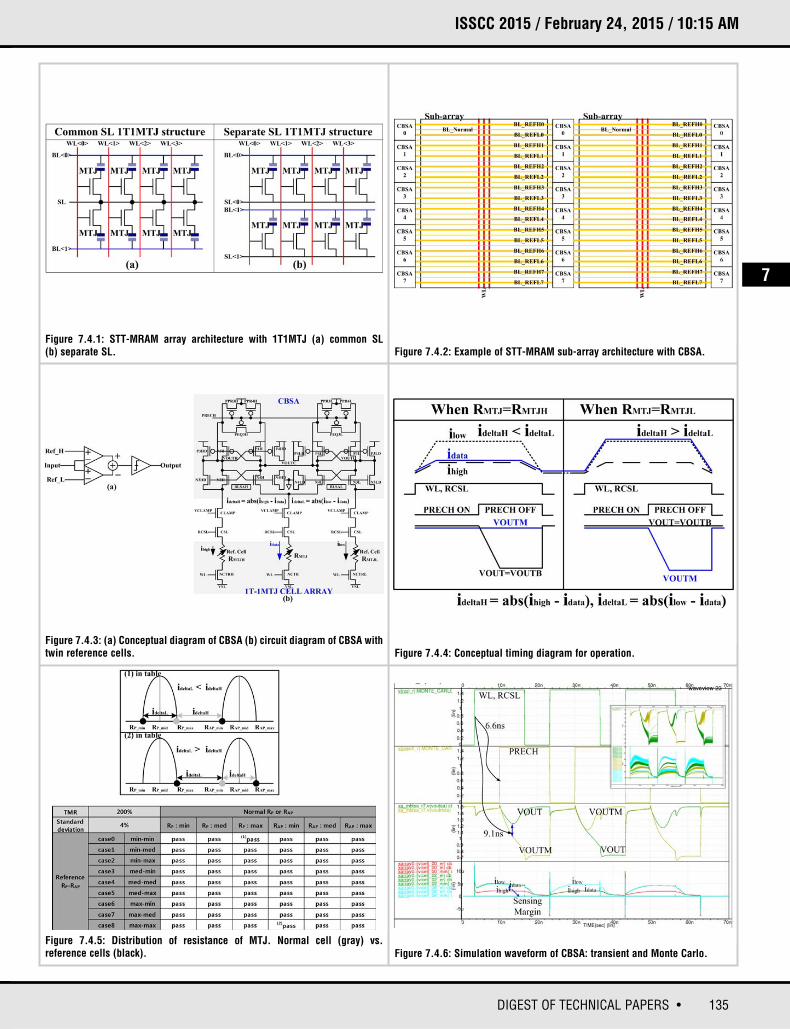
Figure 7.4.1 shows two kinds of STT-MRAM 1T1MTJ array architecture: common SL and separate SL. The unit cell is composed of one NMOS transistorand one MTJ in both cases. In the common SL 1T1MTJ array, every SL is tiedtogether at the top layer with proper bias voltage as shown in Fig. 7.4.1(a). In theseparate SL 1T1MTJ array, a BL and SL pair is needed. Common SL has a compact array architecture, making it more area-efficient than separate SL.Figure 7.4.2 shows an example STT-MRAM sub-array architecture with CBSA.The CBSA can be located at the edge of sub-array while multiple BLs can shareone CBSA together.
Figure 7.4.3(a) shows a conceptual generic diagram of CBSA. The input signalenters two identical side-by-side sense amplifiers (SAs) and the individualresults are merged again in a comparison operation. The upper part ofFig. 7.4.3(b) is the CBSA core, and the lower part of Fig. 7.4.3(b) shows a partof the 1T1MTJ STT-MRAM cell array structure. The CBSA is composed of two
identical cross-coupled latches, pre-charge transistors, and current flowingbranches from CBSA to cell array through two serially connected CLAMP, CSLswitches. PMOS P3H, P4H and NMOS N3H, N4H form one cross-coupled latch,BLSAH which is connected to one of reference cells, and PMOS P3L, P4L andNMOS N3L, N4L form another cross coupled latch, BLSAL which is connectedto another reference cell. Each cross-coupled latch has two current branchesindividually. One of current branches in each cross-coupled latch is directly connected to 1T1MTJ STT-MRAM reference cell, and the remaining currentbranches of both cross-coupled latches are tied together to the common datacell, leading to the name covalent bonded. When CBSA is operating, the currentsflow through three branches at the same time: one is data cell current, idata, theother two are high and low cell reference current, ihigh and ilow. The high and lowreference cell RMTJH/RMTJL need to be programmed before read operations.Because two cross-coupled latches share a current branch with each other,CBSA needs dummy transistors such as P3HD, P4HD, N3HD, N4HD and P3LD,P4LD, N3LD, N4LD for balancing current amount.
In the CBSA scheme, the start and end of sensing operations are controlled bythe PRECH signal as shown in Fig. 7.4.4. When PRECH is low, the output nodesof CBSA are pre-charged or initialized to the supply voltage. During pre-charge,WL and RCSL are turned on, then currents begin to flow through all threebranches of CBSA depending on RMTJ, RMTJH, and, RMTJL. Because the current levels of the three current branches are all different from each other, two identical cross-coupled latches will develop output nodes according to the current condition when PRECH asserts. If the resistance value of the data cell is high, the input current differences of the left cross-coupled latch,ideltaH = abs(ihigh - idata) is almost zero, but that of the right one, ideltaL = abs(ilow - idata) becomes big enough to make BLSAL dominant versusBLSAH. As a result, VOUTL=”0”, VOUTC=”1”, and therefore VOUTH=”0”. If theresistance value of the data cell is low, the complementary values occur. VOUTHhas the same polarity as VOUTL, and covalent-bonded node VOUTC is complementary to both VOUTH and VOUTL.
The RMTJ (RP or RAP) value has significant variation due to process instability andtemperature as shown in Fig. 7.4.5, where it is observed that sensing margin canbe degraded by the variation of normal or reference cells, especially when theTMR of MTJ is not enough. The CBSA is designed to amplify the differencesbetween abs(ilow - idata) and abs(ihigh - idata), rather than those between idata and iref,
(where iref is the mid-level of ilow and ihigh), leading to robustness against RMTJ
variations. In addition, variation of reference cells can track those of normal cellsbecause the CBSA architecture enables them to be located close to each other inthe same array, resulting in better performance and reliability.
Figure 7.4.6 shows simulated waveforms of the operation of the CBSA, includingthe effects of variation of normal and reference cells in both cases that their variations move in the same or opposite directions with different amounts. CBSAoperates correctly until TMR = 200%, σ(RMTJ) = ±4%, σ(RMTJH) = ±4%,σ(RMTJL) = ±4%, showing strong robustness against random variation. MonteCarlo simulations shown in Fig. 7.4.6 include random mismatch of the transistors in the cross-coupled latch and RCTR and RMTJ variation. The resultshows the well-known mismatch sensitivity of the cross-coupled latch, whichcan be managed to be as small as possible by deliberate sizing and laying out.Figure 7.4.7 shows die micrograph of a test-chip which is 3500×1800μm2. Thetest-chip is composed of an 8Mb MRAM cell array, row and column decoders,write drivers, and sensing amplifiers (CBSAs). Each individual sub-array has 512cells per WL and 1024 cells per BL. The density of each sub-array is 0.5Mb. Cellarrays of 1T1MTJ STT-MRAM cells have common SL architecture and one CBSAis shared by 128 BLs and one of which, and therefore its cell, is chosen to beconnected to the CBSA and sensed in a non-destructive way. The table in the figure summarizes the main features of the test-chip.
References:[1] Y. Chen et al., “A 130nm 1.2V/3.3V 16Kb Spin-Transfer Torque RandomAccess Memory With Nondestructive Self-Reference Sensing Scheme,” IEEE J.Solid-State Circuits, vol .47, no .2, pp. 560-573, Feb. 2012.[2] K. Tsuchida et al., “A 64Mb MRAM with Clamped-Reference and Adequate-Reference Schemes,” in IEEE ISSCC Dig. Tech. Papers, pp. 258-260, Feb. 2010.[3] H. Noguchi et al., “Highly Reliable and Low-Power Nonvolatile CacheMemory with Advanced Perpendicular STT-MRAM for High-Performance CPU,”IEEE Symp. VLSI Circuits Dig. Tech. Papers, June 2014.
978-1-4799-6224-2/15/$31.00 ©2015 IEEE
135DIGEST OF TECHNICAL PAPERS •
ISSCC 2015 / February 24, 2015 / 10:15 AM
Figure 7.4.1: STT-MRAM array architecture with 1T1MTJ (a) common SL (b) separate SL. Figure 7.4.2: Example of STT-MRAM sub-array architecture with CBSA.
Figure 7.4.3: (a) Conceptual diagram of CBSA (b) circuit diagram of CBSA withtwin reference cells.
Figure 7.4.5: Distribution of resistance of MTJ. Normal cell (gray) vs. reference cells (black). Figure 7.4.6: Simulation waveform of CBSA: transient and Monte Carlo.
Figure 7.4.4: Conceptual timing diagram for operation.
7

• 2015 IEEE International Solid-State Circuits Conference 978-1-4799-6224-2/15/$31.00 ©2015 IEEE
ISSCC 2015 PAPER CONTINUATIONS
Figure 7.4.7: Die micrograph of test-chip and feature.

136 • 2015 IEEE International Solid-State Circuits Conference
ISSCC 2015 / SESSION 7 / NON-VOLATILE MEMORY SOLUTIONS / 7.5
7.5 A 3.3ns-Access-Time 71.2μW/MHz 1Mb Embedded STT-MRAM Using Physically Eliminated Read-Disturb Scheme and Normally-Off Memory Architecture
Hiroki Noguchi, Kazutaka Ikegami, Keiichi Kushida, Keiko Abe, Shogo Itai, Satoshi Takaya, Naoharu Shimomura, Junichi Ito, Atsushi Kawasumi, Hiroyuki Hara, Shinobu Fujita
Toshiba, Kawasaki, Japan
Nonvolatile memory, spin-transfer torque magnetoresistive RAM (STT-MRAM)is being developed to realize nonvolatile working memory because it provideshigh-speed accesses, high endurance, and CMOS-logic compatibility.Furthermore, programming current has been reduced drastically by developingthe advanced perpendicular STT-MRAM [1]. Several-megabit STT-MRAM withsub-5ns operation is demonstrated in [2]. Advanced perpendicular STT-MRAMachieve ~3× power saving by reducing leakage current in memory cells compared with SRAM for last level cache (LLC) [3]. Such high-speed RAM applications, however, entail several issues: the probability of read disturbanceerror increases and the active power of STT-MRAM must be decreased for higher access speed. Moreover, the leakage power of peripheral circuits must bedecreased, because the high-speed RAM requires high-performance transistorshaving high leakage current in peripheral circuitry [4], limiting the energy efficiency of STT-MRAM. To resolve these issues, this paper presents STT-MRAM circuit designs: a short read-pulse generator with small overheadusing hierarchical bitline for eliminating read disturbance, a charge-optimizationscheme to avoid excessive active charging/discharging power, and ultra-fastpower gating and power-on adaptive to RAM status for reducing leakage power.
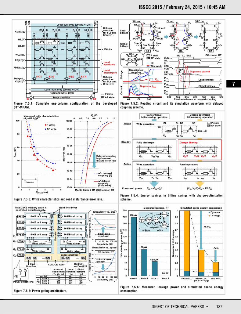
Magnetic tunnel junction (MTJ) has a precession period (1 to 2ns) during whichthe MTJ is immune to thermal influence. MTJ stability increases in inverse proportion to the reduction of the pulse width because of spin-transfer angularmomentum conservation. If the read operation can be terminated with a momentarily sharp cell current during the precession period, read disturbancecan be suppressed. Such a short read pulse generation, however, requires a fine-grain local driver that degrades cell efficiency. Therefore, we implementshort read pulse generation using hierarchal bitlines and delayed timing withoutlocal drivers. Figure 7.5.1 illustrates the memory architecture, which has a hierarchal memory array structure and each local sub-array includes 256 wordlines and four types of local bitlines and global bit/source lines, and 4:1multiplexers. To increase the read speed, differential amplification is used withtwo transistors and two MTJs (2T2MTJ cell) [3]. The 2 MTJs retain complementary states (high- and low-resistance states) that are amplified by avoltage sense amplifier without reference cells. The 2T2MTJ cell area is less thanhalf that of an SRAM cell. In Fig. 7.5.1, column selectors for bitline-left (BL) andbitline-right (BR) connected with delayed column lines (CL) are used for steepread pulse generation. The operation process is shown in Fig. 7.5.2. In thisprocess, two local bitlines R and L are charged, respectively, by the cell currentthrough parallel (P) state and anti-parallel (AP) state MTJs in the first step.Because the local bitline capacitance is small, the charging time is short, andthus the cell current is suppressed. In the next step, global bitlines are chargedby turning on S1 and S2 switches. The voltage difference between the two bitlines is amplified in the last step. For this reason, short read current pulse isgenerated a stable fashion. Figure 7.5.3 presents the simulated read-disturbanceerror rate, indicating that the error rate can be reduced by more than 10×.
Figure 7.5.4 displays energy savings of the charge optimization scheme. For aprior process, to avoid disturbance for half-selected cells when a wordline isactivated, every bitline must be discharged every time before the next cycle. Thisdischarge process consumes energy EBL = CBL∙VW
2, where CBL is the parasiticcapacitance of the bitline, which increases the active power greatly. In contrast,the charge optimization has a mechanism by which the bitline potential chargedto the write potential VW moves to the other bitline discharged to the referencepotential VSS (designated hereafter as charge sharing), so that the potential of thebitlines in the bitline pair is set to be at a floating potential, as shown in Fig. 7.5.4.The additional local equalizers and dischargers used for the charge-optimizationscheme are depicted in Fig. 7.5.1. After the write operation, the equalizer circuitis activated for this charge sharing between the bitline pair. Consequently, writepotential VW and reference potential VSS both become VW/2. Charge sharing
thereby reduces power consumption after the write operation. Because thischarge sharing can be done within a few hundred picoseconds, the latency over-head of the charge sharing is negligible. Furthermore, because the write potentialVW is almost twice as great as the read potential VR, charge sharing sets thepotential of the bitline pair to the read potential VR, which is beneficial for thenext read operation because additional charging to the read potential VR
becomes unnecessary. For the write operation, the potentials of the bitlines areset from the equalized potential to write potentials: VW and VSS. The consumedenergy results in (CBL∙VW/2)∙VW = 1/2∙EBL. Thus, the write energy required for setting the bitlines can be reduced to a half of that of the prior process.Additionally, every bitline pair that is inactive for a long time would be stabilizedat an ideally stable potential and reduced leakage power.
To decrease leakage power in the peripheral circuits, high-speed power gating(HS-PG) for the peripherals is necessary because the stand-by state of high-speed STT-MRAM is extremely short (<50ns). We adopt a fine-grain powerdomain for the STT-MRAM, as presented in Fig. 7.5.5. Power domains are divided into four blocks of 256kb local sub-arrays, decoders, drivers, and SAs.Furthermore, all power-supply lines are classified to local and global powerdomains. Power is supplied to the local memory sub-array power domain onlywhen the sub-array is accessed, which can be judged from the accessedaddress. The global power domain has no such address dependence of PG. Tominimize the area and delay overhead related to HS-PG, we analyze the relationbetween granularity and delay overhead. According to this analysis, the 32KBpower domain is best to achieve sub 4ns access time (Fig. 7.5.5). In thisscheme, during active states, fine-grained PG of the local power domain reducesstatic energy. For long stand-by states, PG of the global power domain canreduce the total stand-by energy more effectively. To detect the long-stand-bystates, we adopt timer-based state transition. As shown in Fig. 7.5.5, state 0 represents the read or write operation state, state 1 represents the non-operationstate where every local power domain is powered off, and state 2 representsglobal power gated state in which state every local power domain and globalpower domain is powered off. In state 1, the power-gated domain can be powered on quickly. In state 2, the power-on process requires several cycles.The on-off energy overhead is negligible, although state 2 can reduce stand-bypower more effectively than state 1.
Figure 7.5.6 presents the measurement results. A chip micrograph of 1Mb non-volatile memory in 65nm CMOS technology is displayed in Fig. 7.5.7. Themacro area including power switches was 0.82mm2 with 57.6% cell efficiency.The read access time is 3.3ns at 1.2V. The measured energy consumptions ofread and write operations are, respectively, 71.2μJ/MHz and 166.2μJ/MHz. Therespective stand-by power measurements obtained in state 1 and in state 2 are44.6μW and 80nW, while 178μW stand-by power is consumed without PG, asdepicted in Fig. 7.5.6. Furthermore, the measured on-off latency of state 2 is21ns. The energy performance of LLC was evaluated using a customized cycle-accurate CPU simulator [3]. In the prior STT-MRAM LLC, total cachepower is reduced by more than 59% compared to SRAM-based LLC because theSTT-MRAM cell consumes zero stand-by leakage without PG. With HS-PG, STT-MRAM-based LLC can reduce static energy including peripherals by a further 54% compared to the prior STT-MRAM based LLC.
Acknowledgments:The authors thank Professor Hiroshi Nakamura and his research group atUniversity of Tokyo for discussion related to CPU architectures. This work waspartly supported by NEDO in Japan.
References:[1] K. Ikegami et al., “Low power and high density STT-MRAM for embeddedcache memory using advanced perpendicular MTJ integrations and asymmetriccompensation techniques,” IEDM Tech. Dig., S28-1, Dec. 2014.[2] G. Jan et al., “Demonstration of fully functional 8Mb perpendicular STT-MRAM chips with sub-5ns writing for non-volatile embedded memories,” Symp.VLSI Technology Dig. Tech. Papers, pp. 42-43, June 2014. [3] H. Noguchi et al., “Highly reliable and low-power nonvolatile cache memorywith advanced perpendicular STT-MRAM for high-performance CPU,” Symp.VLSI Circuits Dig. Tech. Papers, pp. 97-98, June 2014.[4] E. Arima et al., “Fine-grain power-gating on STT-MRAM peripheral circuitswith locality-aware access control,” Memory Forum (in conjunction with ISCA),June 2014.
978-1-4799-6224-2/15/$31.00 ©2015 IEEE
137DIGEST OF TECHNICAL PAPERS •
ISSCC 2015 / February 24, 2015 / 10:45 AM
Figure 7.5.1: Complete one-column configuration of the developed STT-MRAM.
Figure 7.5.2: Reading circuit and its simulation waveform with delayed coupling scheme.
Figure 7.5.3: Write characteristics and read disturbance error rate.
Figure 7.5.5: Power gating architecture.Figure 7.5.6: Measured leakage power and simulated cache energy consumption.
Figure 7.5.4: Energy savings in bitline swings with charge-optimizationscheme.
7

• 2015 IEEE International Solid-State Circuits Conference 978-1-4799-6224-2/15/$31.00 ©2015 IEEE
ISSCC 2015 PAPER CONTINUATIONS
Figure 7.5.7: Chip micrograph and measured shmoo plots.

138 • 2015 IEEE International Solid-State Circuits Conference
ISSCC 2015 / SESSION 7 / NON-VOLATILE MEMORY SOLUTIONS / 7.6
7.6 1GB/s 2Tb NAND Flash Multi-Chip Packagewith Frequency-Boosting Interface Chip
Hyun-Jin Kim, Jeong-Don Lim, Jang-Woo Lee, Dae-Hoon Na, Joon-Ho Shin, Chae-Hoon Kim, Seung-Woo Yu, Ji-Yeon Shin, Seon-Kyoo Lee, Devraj Rajagopal, Sang-Tae Kim, Kyeong-Tae Kang, Jeong-Joon Park, Yong-Jin Kwon, Min-Jae Lee, Sung-Hoon Kim, Seung-Hoon Shin, Hyung-Gon Kim, Jin-Tae Kim, Ki-Sung Kim, Han-Sung Joo, Chan-Jin Park, Jae-Hwan Kim, Man-Joong Lee, Do-Kook Kim, Hyang-Ja Yang, Dae-Seok Byeon, Ki-Tae Park, Kye-hyun Kyung, Jeong-Hyuk Choi
Samsung Electronics, Hwaseong, Korea
NAND Flash-based solid-state drives (SSDs) have been adopted in enterprisestorage applications that require high capacity and high-throughput performance. In recent years, a SATA interface supporting only up to 600MB/sthroughput has hindered the accelerating performance growth of SSDs due tothe host bandwidth limit. A PCI Express (PCIe) has emerged to close the limitbecause it can deliver 1GB/s throughput per lane and can be scaled to multi-laneto improve bandwidth [1]. Accordingly, the SSD performance bottleneck hasmoved from the host interface to the NAND flash interface. In a memory system,a die-stacking technology in a NAND flash multi-chip package (MCP) effectivelyincreases capacity and throughput performance in terms of PCB complexitiesand power consumption compared to a method increasing the number of channels. However, the multi-drop bus topology on NAND interfaces severelyaffects I/O speed degradations due to channel reflections and inter-symbol interference (ISI) resulting from large capacitive loadings [2]. The undeniableparadox between larger storage capacity and higher I/O bandwidth has becomea key challenge to reach enterprise-class SSDs. To overcome this issue, thispaper presents a frequency-boosting interface chip (F-Chip) to boost I/O speedswhile meeting capacity requirements. A 2Tb NAND flash MCP with 1GB/s toggleDDR interface is accomplished by incorporating the F-Chip into the NAND MCPincluding a 16-die stacked 128Gb NAND flash [3].
Figure 7.6.1 illustrates a conceptual architecture of the F-Chip embedded in theNAND Flash MCP. The hardware architecture of SSDs is generally composed ofmemory controllers, NAND flash memories and DRAMs. The F-Chip realizes apoint-to-point topology on I/O buses between memory controllers and the F-Chip suffering from undesired reflections at stubs in channels. In addition, theF-Chip reduces by half the capacitive loadings on the F-Chip-to-NAND interfacesby implementing and evenly distributing two internal I/O buses between the F-Chip and NAND devices.
The F-Chip supports a retiming mode to transfer I/O signals from the memorycontrollers to the NAND devices. During the retiming mode, the F-Chip retimesdata using an internally generated clock to reduce skews and extend data validwindow. A time-to-digital-converter (TDC) based clock generator is implementedto generate the sampling clock. The key feature of the clock generator is a fastlock time, which is essential for the asynchronous toggle DDR interface thatdoes not support a free-running clock signal. Moreover, we can hide the locktime during the period of /RE-to-DQS delay (tDQSRE) defined in the toggle DDRspecification because the lock information can be ready before DQS and data aretransferred to the F-Chip from NAND devices.
The F-Chip also improves reduced timing margins due to inherent timing jitterthat occurs in NAND devices with an asynchronous interface. Thus, the F-Chipperforms data de-serialization and serialization to increase timing margins whilereceiving and aligning incoming data. Additionally, the F-Chip includes a dutycycle corrector (DCC) to improve jitter due to the duty-cycle distortion of incoming DQS from NAND devices. Figure 7.6.2 describes an open-loop DCCscheme with a sequential phase interpolator (SPI) and a two-stage Schmitt trigger. The SPI uses multiple inverter stages and each of them is turned on in asequential manner with the controllable delay to vary resistances and capacitances. The delays are optimized depending on the target frequency toprovide better phase blending for wider operating-frequency ranges. The two-stage Schmitt trigger is developed to prevent undesired toggle at the outputof the phase interpolator. Unlike the synchronous clock, the /RE can start andstop toggling at any times during read operations. Insufficient hysteresis afterthe /RE stops toggling would result in an extra toggle, causing critical functionalfailure. The two-stage Schmitt trigger provides sufficient high-to-low hysteresis
and low-to-high hysteresis by implementing MN4 and MN3, respectively, toblock the extra toggle.
Figure 7.6.3 presents a method of calibrating NAND driver strengths (DS) by utilizing ZQ calibration and on-die termination (ODT) implemented in the F-Chip.ZQ calibration has broadly used for better signal integrity over process, voltageand temperature (PVT) variations. On the other hand, external reference resistors for ZQ calibration on each NAND device cannot be easily equipped dueto constraints on PCB space and package balls. In order to eliminate the constraints, the F-Chip trims all the NAND DS using the calibrated F-Chip DS.The F-Chip detects the DS offsets of NAND devices by comparing the output levels of NAND devices with the VREF in the F-Chip while the ODT of the F-Chipis turned on and the VREF level is digitally controlled. The output codes of thecomparators are monitored at external I/O PADs, and are applied to compensatethe DS offsets of NAND devices. The ZQ calibration implemented in the F-Chipuses an internal active resistor to remove constraints on packages as well. Sincethe reference resistor for ZQ calibration needs to be precise, the process variations of the active resistor are trimmed at wafer-level, and its temperaturevariations are also compensated by calibrating the ZQ level using a temperaturesensor.
This paper also tackles testing methods because the F-Chip-to-NAND interfacescannot be monitored directly, and thus the NAND flash adopting F-Chip mighthave difficulties in analyzing internal I/O timing margins. Therefore, the F-Chipuses an alternative method that implements selective loop-back paths and feedsthe signals at each path back to external I/O PADs. Figure 7.6.4 depicts a conceptual diagram of I/O design for test (DFT) scheme. Besides the loop-backtest mode, the DFT block measures internal timing delays between DQS and dataon the F-Chip-to-NAND interfaces using TDC and the embedded data patterngenerator. The output codes of TDC are monitored while the delay codes for DQSare calibrated [4]. The codes are applied to optimize timing margins betweenDQS and data on the F-Chip-to-NAND interfaces.
The F-Chip is fabricated in a 35nm 1.8V CMOS process and occupies5.5807mm2. Figure 7.6.5 shows the measured eye diagrams of NAND flash MCPat 1Gb/s with and without F-Chip. Compared to the 1Tb NAND flash MCP with 8-die stacking, the 2Tb NAND flash MCP combining 16-die stacked NAND and F-Chip shows 22% improvement in eye-opening performance even at the largernumber of die-stacking. Moreover, the horizontal eye opening of the 1Tb NANDMCP with 8-die stacking is 380ps at 1Gb/s, which is not wide enough to meettiming requirement. In Figure 7.6.6, test results of horizontal eye opening arealso compared according to the I/O data rates, and simulation results for 16-diestacked NAND flash without F-Chip are additionally described. As a result, thetiming margins of NAND flash MCP with over 8-die stacking are drasticallyreduced as the I/O data rates increase, and thus the required NAND I/O timingbudget cannot be met in the memory system without F-Chip. In addition, the 2TbNAND MCP employing the F-Chip decreases I/O power consumption by 25%compared to the case without F-Chip because the F-Chip structurally lowers thepin capacitances and controls the interleaved operations of two internal I/Obuses to save power. Therefore, the F-Chip cost-effectively enables the 2TbNAND flash MCP with 1GB/s toggle DDR interface. The die micrograph of the F-Chip is provided in Figure 7.6.7.
References:[1] www.pcisig.com [2] W. Shin, G. Hong, H. Lee, J. Han, S. Kim, K. Park, D. Lim, J. Chun, D. Jeong,and S. Kim, “A 4.8Gb/s impedance-matched bidirectional multi-drop transceiverfor high-capacity memory interface,” ISSCC Dig. Tech. Papers, pp. 494-495,Feb. 2011. [3] Ki-Tae Park, et al., “Three-dimensional 128Gb MLC vertical NAND Flash-memory with 24-WL stacked layers and 50MB/s high speed programming,”ISSCC Dig. Tech. Papers, pp. 334-335, Feb. 2014. [4] D. Fick, N. Liu, Z. Foo, M. Fojtik, J. Seo, D. Sylvester, D. Blaauw, “In SituDelay-Slack Monitor for High-Performance Processors Using An All-Digital Self-Calibrating 5ps Resolution Time-to-Digital Converter,” ISSCC Dig. Tech. Papers,pp. 188-189, Feb. 2010.
978-1-4799-6224-2/15/$31.00 ©2015 IEEE

139DIGEST OF TECHNICAL PAPERS •
ISSCC 2015 / February 24, 2015 / 11:15 AM
Figure 7.6.1: Conceptual architecture of the F-Chip embedded in NAND flashMCP including 16-die stacked NAND Flash.
Figure 7.6.2: DCC scheme with sequential phase interpolator and two-stageSchmitt trigger.
Figure 7.6.3: Method of calibrating NAND driver strength by utilizing ODT andZQ calibration implemented on F-Chip.
Figure 7.6.5: Measured eye diagram of NAND flash MCP at 1Gb/s with andwithout F-Chip.
Figure 7.6.6: Test results of horizontal eye opening showing the effect of F-Chip.
Figure 7.6.4: Conceptual block diagram of I/O DFT.
7

• 2015 IEEE International Solid-State Circuits Conference 978-1-4799-6224-2/15/$31.00 ©2015 IEEE
ISSCC 2015 PAPER CONTINUATIONS
Figure 7.6.7: Die micrograph of F-Chip.

140 • 2015 IEEE International Solid-State Circuits Conference
ISSCC 2015 / SESSION 7 / NON-VOLATILE MEMORY SOLUTIONS / 7.7
7.7 Enterprise-Grade 6× Fast Read and 5× Highly Reliable SSD with TLC NAND-Flash Memory for Big-Data Storage
Tsukasa Tokutomi, Masafumi Doi, Shogo Hachiya, Atsuro Kobayashi, Shuhei Tanakamaru, Ken Takeuchi
Chuo University, Tokyo, Japan
An enterprise-grade SSD with TLC (3b/cell) NAND Flash is presented with threetechniques that achieve high speed and high reliability. Quick low-density parity-check (LDPC) reduces the read latency of 1Xnm TLC NAND Flash SSD by83%. Dynamic VTH optimization and auto data recovery reduce the NAND Flashbit-error rate (BER) by 80% and 18%, respectively. These techniques can beimplemented in the SSD controller without circuit overhead. No modification isrequired to the TLC NAND flash.
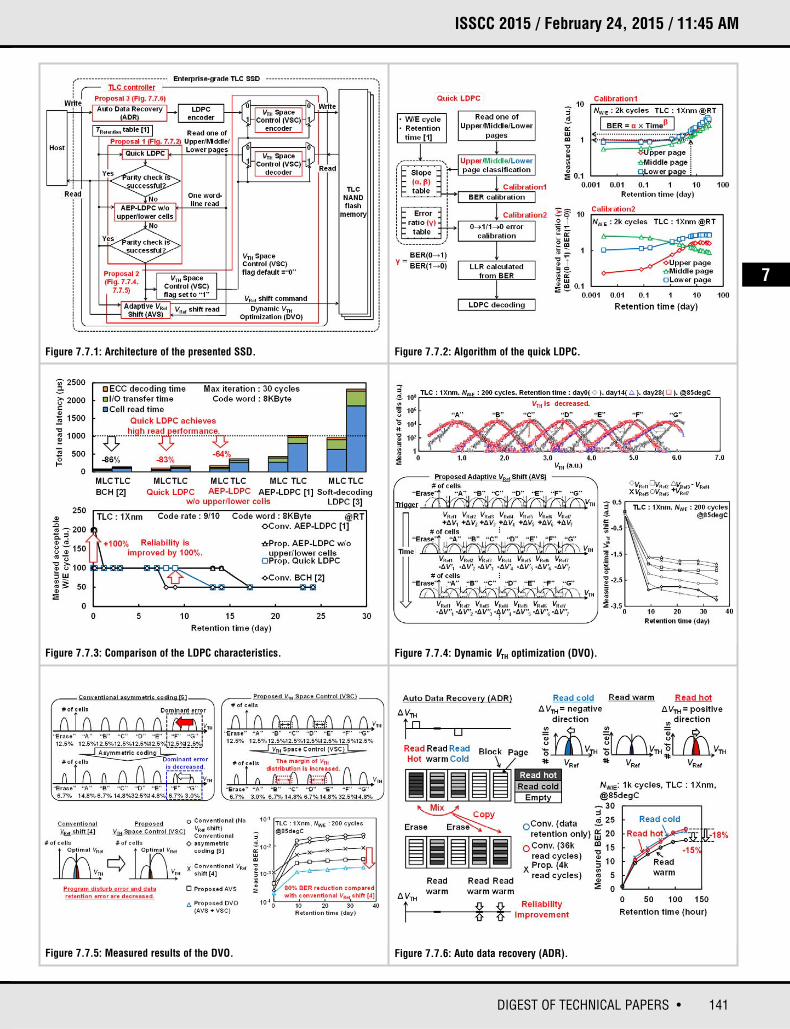
Enterprise storage demands fast speed and good reliability with high-density forbig data applications. Though TLC NAND Flash SSD has the bit cost advantageover MLC (2b/cell) NAND Flash SSD, the adoption in the enterprise market islimited due to its poor speed and reliability. Real-time online analytical processing (OLAP) applications require a quick response from SSD. In real-world workloads, temporal data locality causes read requests to concentrateon the same memory cells. The frequently read data (hot data) suffers from theread disturb while cold data fail due to the data retention. To overcome performance and reliability problems of TLC NAND flash SSD, this paperdescribes three techniques shown in Fig. 7.7.1.
To efficiently correct errors with a short latency, this paper presents quick LDPC.The read latency is 83% lower than advanced error-prediction LDPC (AEP-LDPC)error-correcting code (ECC) [1]. When memory cells wear-out and errors exceedthe ECC capability, dynamic VTH optimization adaptively selects the optimal readreference voltage (VRef) and increases the VTH read margin. As a result, measurederrors are reduced by 80%. Auto data recovery compensates the VTH decrease(the data retention error) with the VTH increase (the read disturb error).
First, the LDPC is shown in Fig. 7.7.2. Figure 7.7.3 shows the total read latencyand the measured reliability. In the enterprise MLC NAND Flash SSD, fast BCHECC [2] is used. The error-correction capability of BCH is not sufficient for theenterprise use of TLC NAND Flash because enterprise storage requires higherendurance than consumer storage. The soft-decoding LDPC [3] corrects moreerrors than BCH ECC. However, it needs analog VTH to calculate the log-likelihood ratio (LLR) and 49-time VRef sensing is necessary and the read latencyincreases to 2.3ms. VRef sensing is defined as sensing a memory cell with one ofthe reference level. The conventional AEP-LDPC estimates LLR by the hard-decision (digital) VTH, the write/erase (W/E) cycle, the retention time and inter-cell coupling information. Since the analog VTH is not used, the read latencydecreases to 1ms. Yet, AEP-LDPC is still 7× slower than BCH ECC. In AEP-LDPC,21-time VRef sensing are required to read neighboring cell data in both wordlineand bitline directions.
To accelerate the read while securing the high reliability, the quick LDPC readsonly one of upper/middle/lower pages, corresponding to 2 to 3VRef sensing. Thetotal read latency is 173μs, which is comparable with the latency of BCH ECC of146μs. The TLC controller estimates LLR by using the W/E cycle, retention timeand several tables. In Calibration 1, BER is estimated by referring to a slope tablethat indicates BER for the given W/E cycle and the retention time. At Calibration2, each BER of 0→1 and 1→0 error is calculated by referring to error-ratio tablethat stores the error ratio for each W/E cycle and retention time. The error ratiois defined as the ratio of 0→1 to 1→0 errors. If it is greater than 1, the originaldata is more likely to be 0 than 1. The TLC controller estimates LLR and thenexecutes the LDPC decoding. Quick LDPC increases the W/E cycle by 100% witha similar read latency as BCH ECC. Quick LDPC is 83% faster than AEP-LDPC.
For applications with very high endurance, when quick LDPC fails to correcterrors, AEP-LDPC without upper/lower cells is executed. A whole wordline dataare read by 7VRef sensing. Neighboring cell data in the bitline (column) directionis used to cancel the inter-cell capacitive coupling. Compared with quick LDPC,the W/E cycle extends by 100% and the read latency increases to 373μs. Notethat the cell data at the next wordline (row) is not used to avoid the excessiveread speed penalty.
Second, dynamic VTH optimization (DVO) is shown in Figs. 7.7.4 and 7.7.5. DVOis composed of adaptive VRef Shift (AVS) and VTH space control (VSC). AVS adaptively adjusts the read reference voltage (VRef) to minimize errors for eachretention time. During the data retention, VTH at the higher VTH state such as “G”decreases faster than that of the lower VTH state such as “A”. Conventionally,when ECC cannot correct errors, VRef is decreased by a fixed voltage [4] then theread operation is retried. However, the measured VTH shift of “A” to “G” statesstrongly depends on the data retention time. The transient VTH shift cannot becompensated by the conventional approach. To track the dynamic VTH shift, AVSadaptively selects the optimal VRef based on the retention time. The optimal VRef
is stored in the VRef table.
When the error recovery of AVS is not enough, VSC is applied as shown inFig. 7.7.5. VSC optimizes the space between “A” to “G” states without changingthe write sequence of NAND Flash. Since the VTH shift during the retention differsamong states “A” to “G”, the space should also be optimized. In [5], asymmetriccoding is proposed to improve the reliability of NAND Flash by decreasing thepopulation of the worst state “G” that causes the most data retention errors. IfVRef is adjusted by AVS, asymmetric coding is unnecessary. In Fig. 7.7.5, thepopulation of “C” and “E” are increased while those of “B” and “D” aredecreased. As the space from “B” to “C” and “D” to “E” are increased, the dataretention errors of “C” and “E” are decreased. If only AVS is applied, errorsdecrease by 61%. By combining AVS and VSC, errors decrease by 80%. VSC isused only in systems that require extremely high reliability because VSC has 6to 25% flag bit penalty.
Third, auto data recovery (ADR) is shown in Fig. 7.7.6. In enterprise servers, ahigh temporal locality exists among read data. Thus, the read requests concentrates on the same memory cells. The frequently read data is hot data andothers are cold data. The NAND Flash blocks storing hot data suffer from theread disturb, while the data retention error occurs in blocks with cold data. ADRmixes both hot and cold data in the same block to compensate errors. The readdisturb increases VTH of unselected cells in the same block and the data retentiondecreases VTH. By mixing hot and cold data, VTH increase and decrease are compensated. As a result, the read disturb error of hot data and the data reten-tion error of cold data decrease by 18% and 15%, respectively.
Figure 7.7.7 shows the photograph of the measured SSD [6]. Quick LDPCdecreases the read latency by 83% compared with AEP-LDPC. When the memory cell errors exceed the ECC capability, Dynamic VTH optimizationdecreases errors by 80%. Also, auto data recovery decreases errors by 18% byevenly distributing the hot and cold data in the NAND flash blocks. Because thetotal table size is only 403kB per 128Gb TLC NAND Flash chip, tables can bestored in the NAND flash without capacity penalty.
Acknowledgment:This work is partially supported by CREST/JST. The authors appreciate C. Sunand C. Matsui for their support.
References:[1] T. Tokutomi et al., “Advanced Error Prediction LDPC for High-Speed ReliableTLC NAND-based SSDs,” IMW, pp. 99-102, May 2014.[2] Y. Lee et al., “6.4Gb/s Multi-Threaded BCH Encoder and Decoder for Multi-Channel SSD Controllers,” ISSCC Dig. Tech. Papers, pp. 426-428, Feb. 2012.[3] C. Kim, et al., “A 21nm High Performance 64Gb MLC NAND Flash memorywith 400MB/s Asynchronous Toggle DDR Interface,” J. Solid-State Circuits,pp. 981-989, April 2012.[4] T. Parnell, “Flash Controller Design,” IMW, Tutorial, May 2014.[5] S. Tanakamaru et al., “95%-Lower-BER 43%-Lower-Power Intelligent Solid-State Drive (SSD) with Asymmetric Coding and Stripe Pattern EliminationAlgorithm,” ISSCC Dig. Tech. Papers, pp. 204-205, Feb. 2011.[6] S. Tanakamaru et al., “Hybrid Storage of ReRAM/TLC NAND Flash with RAID-5/6 for Cloud Data Centers,” ISSCC Dig. Tech. Papers, pp. 336-337, Feb. 2014.
978-1-4799-6224-2/15/$31.00 ©2015 IEEE
141DIGEST OF TECHNICAL PAPERS •
ISSCC 2015 / February 24, 2015 / 11:45 AM
Figure 7.7.1: Architecture of the presented SSD. Figure 7.7.2: Algorithm of the quick LDPC.
Figure 7.7.3: Comparison of the LDPC characteristics.
Figure 7.7.5: Measured results of the DVO. Figure 7.7.6: Auto data recovery (ADR).
Figure 7.7.4: Dynamic VTH optimization (DVO).
7

• 2015 IEEE International Solid-State Circuits Conference 978-1-4799-6224-2/15/$31.00 ©2015 IEEE
ISSCC 2015 PAPER CONTINUATIONS
Figure 7.7.7: Photograph of the measured SSD [6] and the summary of thiswork.