seu hardening techniques for retargetable ,...
TRANSCRIPT
SEU Hardening Techniques forRetargetable, Scalable, Sub-Micron
Digital Circuits and Libraries*
M. P. Baze, J. C. Killens, R. A. Paup, W. P. SnappBoeing Space and Communications
Seattle, WA
* Work supported by DTRA contract DTRA01-00-C-0046

5/1/2002 2
“Multi-Fab” IC Design Environment
Multi-Fab environments may be –
• Manufacturing design house possessing several processes
– usually with some process similarity
• “Fabless” design house with access to several processes via
-Single manufacturer with several processes
-Third party interface, i.e. MOSIS
-Independent agreements with several manufacturers

5/1/2002 3
“Multi-Fab” Issues
• Advantage of Multi-Fab Environment
Utilization of different fabrication processes as design options
Accomplished by“Retargeting” designs to different process technologies.
or“Scaling” designs to smaller rules in same technology.
• Retargetability – Ease of design transfer to different process.
Bulk, EPI, N-Well, P- Well, Twin Tub, SIMOX, SOS, SOI-MESA,Twin Tub, Single Poly, Dual Poly, # Metal Layers, Resistor Types,Capacitor Types, Device Models, etc.
• Scalability – Ease with which a design can be scaled down infeature size, without sacrificing the advantages of scaling.

5/1/2002 4
Retargeting and Scaling Designs
VHDLDesign A (8051)
VHDLDesign B (1773)
VHDLDesign C (BC30)
Library B
Library B/2
Synthesis
Library AProcess A
Process B
Process B/2
Standard DigitalCell Functions
Targeting / Scaling

5/1/2002 5
Retargeting and Scaling Designs
VHDL (H1, 2, 3)Design A (8051)
VHDL (H2, H3)Design B (1773)
VHDL(H1, H3)Design C (BC30)
B-1
B/2-3
Synthesis
A-1Process A
Process B
Process B/2
HARD 2
Targeting / Scaling
SEU Hardening cap.s, filters, redundant, Idrive, etc.
HARD 1 HARD 3
A-2
B-2
A-3
B/2-2

5/1/2002 6
Basic SEU Hardening Options
Three Categories of SEU Hardening Techniques
1. Charge Dissipation - Consumes power
2. Temporal Filtering - Reduces speed
3. Spatial Redundancy - Consumes area
• Charge Dissipation & Temporal Filtering - Increase LETT
• Spatial Redundancy – Reduce effective X-section

5/1/2002 7
Increase Transistor Current Drive VDD
VSS
IN0
IN1
OUT
“STANDARD”NAND2
HARDENEDNAND2
VDD
VSS
IN0
IN1
OUT•Scalability
Speed – no significant penalty
Area – in proportion to drive
Power – in proportion to drive
Charge Dissipation
transistor IDRIVE > QCOL / Register TSH
Sink QCOL to prevent “valid” pulse widths
where “valid” > register TSH
• Retargetability
Increases area ofstandard celllibrary
5/1/2002 8
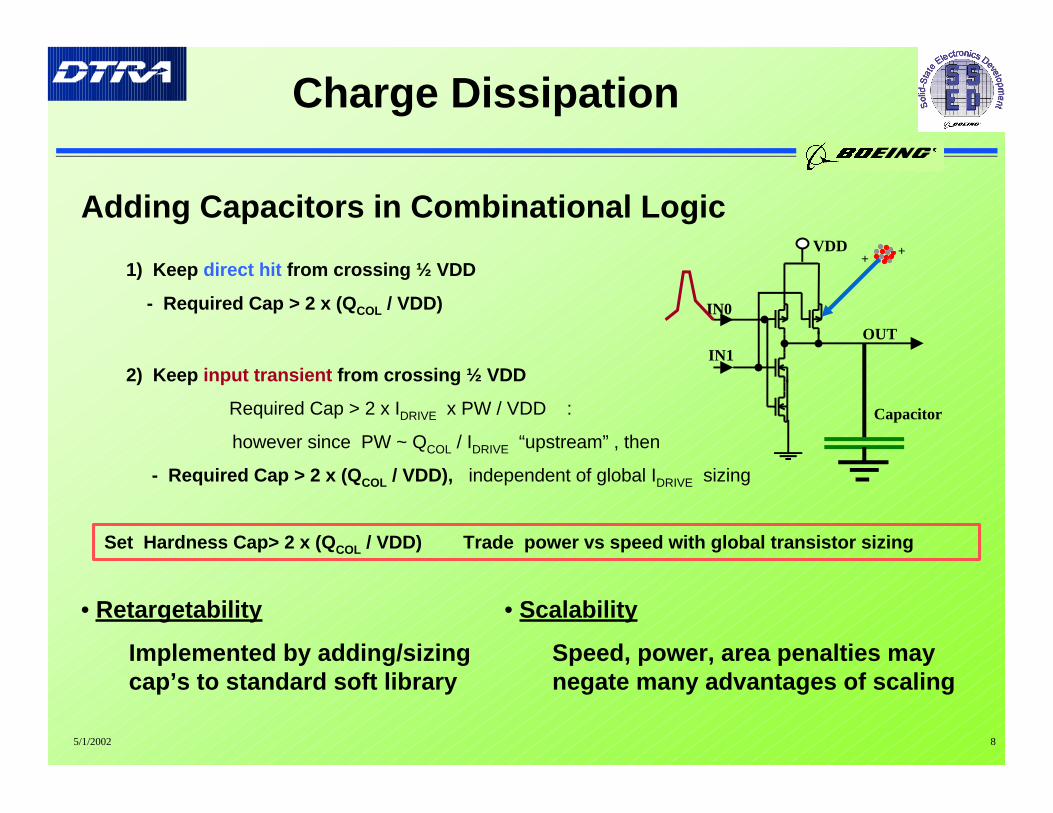
Charge Dissipation
• Retargetability
Implemented by adding/sizingcap’s to standard soft library
Adding Capacitors in Combinational Logic
IN0
IN1OUT
VDD
Capacitor
1) Keep direct hit from crossing ½ VDD
- Required Cap > 2 x (QCOL / VDD)
2) Keep input transient from crossing ½ VDD
Required Cap > 2 x IDRIVE x PW / VDD :
however since PW ~ QCOL / IDRIVE “upstream” , then
- Required Cap > 2 x (QCOL / VDD), independent of global IDRIVE sizing
++
• Scalability
Speed, power, area penalties maynegate many advantages of scaling
Set Hardness Cap> 2 x (QCOL / VDD) Trade power vs speed with global transistor sizing

5/1/2002 9
Adding Capacitors in sequential logic
Capacitor
• Retargetability
Implemented by adding/sizingcap’s to standard soft library
• Scalability
Speed, power penalties may negatemany advantages of scaling
2) Lengthen TSH - short input transients “invalid”
Register TSH > QCOL / transistor IDRIVE
++
1) Keep direct hit from crossing ½ VDD
- Required Cap > 2 x (QCOL / VDD)
Charge Dissipation / Temporal Filtering

5/1/2002 10
VotingCircuit
in Combinationallogic
Network
out
“Delay-and-Vote”
Temporal Filtering
Total Delay = 2 x Error Pulse Width ~ 2 x (QCOL / IDRIVE )
if IDRIVE = 0.25 mA and QCOL = 0.4 pC then 2 x (QCOL / IDRIVE ) = 3.2 ns
• Retargetability
Architecture implementation.Delay element redesign foreach process.
• Scalability
If QCOL does not scale down withIDRIVE, the required delay increases
delay
delay delay

5/1/2002 11
VotingCircuit
INPUTS
Logic Network
OUT
Spatial Redundancy - TMR
Triple Mode Redundancy (TMR)
Logic Network
Logic Network
Error on OUT requires simultaneouserrors in 2 or more logic networks
• Does not increase LET threshold
• Does reduce effective cross-section by
geometric probability of multiple node hit
X-sec EFF ~ 1 / (node separation)2 ~3X power and area penalty
• Retargetability
Architecture implementation.Modified structural netlists and/orcells
• Scalability
Adequate separation is critical

5/1/2002 12
Bad Layout Practice
- “Rail stacking” of voted F/F’s
Adjacent redundantelements
CLR
PRE
CLK
DQ
CLR
PRE
CLK
DQ
voter Q
1
3
2
TMR - Node Separation
Triple Redundant Flip/flops
Vdd
Vdd

5/1/2002 13
CLR
PRE
CLK
D QCLR
PRE
CLK
D QCLR
PRE
CLK
D Q
voterQ
1 2 3
• Acceptable Layout
- “Sequencing” of voted F/F’s
Places redundant elements at greater distance
TMR - Node Separation
Triple Redundant Flip/flopsVdd

5/1/2002 14
Internally Redundant Logic
OUT
Ndrive
N isolation
P isolationPshunt
Nshunt
IN
Pdrive
Places redundant nodes in very close proximity - Cell layout criticalVdd
Vdd
PBPA
PC
NC
NA
NB
Pout
Nout
Vdd
Vdd
PBPA
PC
NC
NA
NB
Pout
Nout
• Retargetability
Non-standard library cells.Transistors often need sizing tomaintain performance.
• Scalability
Adequate separation is critical
Isolated Well Transistors*
“Dual Data Stream”redundant logic**
*Baze, et, al. IEEE NSREC ’00, pg 2609 **Wiseman, IEEE Rad. Data Workshop, ’94, pg51
5/1/2002 15
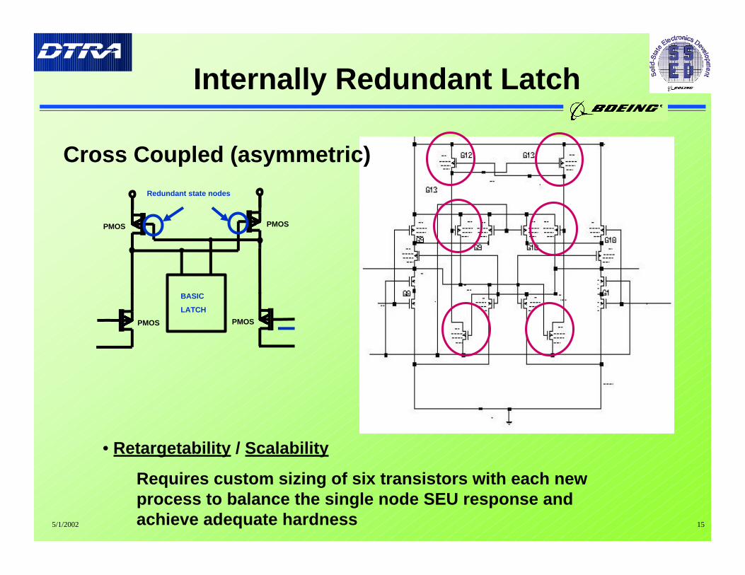
Cross Coupled (asymmetric)
• Retargetability / Scalability
Requires custom sizing of six transistors with each newprocess to balance the single node SEU response andachieve adequate hardness
BASIC
LATCH
Redundant state nodes
PMOS
PMOS PMOS
PMOS
Internally Redundant Latch

5/1/2002 16
clock
data
DICE* - Dual interlocked storage cell
Less sensitive to transistor sizing
*Calin, et al, IEEE NSREC ’96, pg2877 **Alexander, et al. GOMAC 2001 Digest of Papers, pg 257
**
Internally Redundant Latch
Table 2. Single Event Effects Test Results **

5/1/2002 17
CLK
CLKB1
CLK
CLKB2Q
CLR
PRE
D
Low Power DICE Latch with PRE / CLR
CLKB2CLK
CLKB1
CLK
CLKB2
CLK
CLKB1CLK
• Low Power – pass gates
• Clear
• Preset
• Output buffer

5/1/2002 18
CLK
CLKB1
CLK
CLKB2Q
CLR
PRE
D
DICE Latch Layout Restrictions
CLKB2CLK
CLKB1
CLK
CLKB2
CLK
CLKB1CLK
No two same colortransistor blocks maybe paced side by side

5/1/2002 19
DICE Flip/Flop
• Retargetability
Transistor sizing and pass gate/ logicimplementations may need to betraded to optimize speed vs. power
• Scalability
Single node hardnessinsensitive to transistor sizing.Node separation is critical
CLK
CLKB2
CLK
CLKB2CLK
CLKB1CLK
CLKB1
CLKB1
Q
CLR
PRE
D CLKB1
CLK
CLK
CLK
CLK
CLK
CLKB2
CLKB2
CLKB2
CLK
CLKB1

5/1/2002 20
Flip/Flop Comparisons
Std Low Power
Low Powertriplicate-and-vote
Increased IDRIVE
DICE
POWER
(CLK-Q)
SPEED
(TSH)
HARDNESS*
(e/b-d)AREA
(µµm2)
10-8
1 node
Rise – 0.7 µµW
Fall – 0.2 µµW
Rise – 1.0 µµW
Fall – 0.2 µµW
Rise – 1.72 µµW
Fall – 1.27 µµW
Rise – 1.4 µµW
Fall – 1.1 µµW
Rise – 0.21 ns
Fall – 0.27 ns
Rise – 0.16 ns
Fall – 0.15 ns
Rise – 0.21 ns
Fall – 0.27 ns
Rise – 0.96 ns
Fall – 0.97 ns
360
460
1200
520
2x10⁻⁹
1 node
10-11
2 node
1.6 x10⁻¹⁰
2 node
• Retargetable / Scalable Flip/Flops in a Single Process
*preliminary estimates for a proposed SOI process, GEO orbit

5/1/2002 21
Summary
A number of design options exist forimproving the SEU hardness of digital logic.
However, specific considerations andrestrictions must be observed for eachtechnique if these techniques are to be appliedover a range of process technologies andreduced feature size.