shedding too much light on a microcontroller’s firmware ... · shedding too much light on a...
TRANSCRIPT

Shedding too much Light on a Microcontroller’s Firmware Protection
Johannes ObermaierFraunhofer Institute AISEC
Stefan TatschnerFraunhofer Institute AISEC
Abstract
Almost every microcontroller with integrated flash fea-tures firmware readout protection. This is a form of con-tent protection which aims at securing intellectual prop-erty (IP) as well as cryptographic keys and algorithmsfrom an adversary. One series of microcontrollers arethe STM32 which have recently gained popularity andthus are increasingly under attack. However, no practicalexperience and information on the resilience of STM32microcontrollers is publicly available. The paper presentsthe first investigation of the STM32 security concept, es-pecially targeting the STM32F0 sub-series. Starting witha conceptual analysis, we discover three weaknesses anddevelop them to vulnerabilities by demonstrating corre-sponding Proofs-of-Concept. At first, we discover that acommon security configuration provides low protectionwhich can be exploited using our Cold-boot Stepping ap-proach to extract critical data or even readout-protectedfirmware. Secondly, we reveal a design weakness in thesecurity configuration storage which allows an attackerto downgrade the level of firmware protection, therebyenabling additional attacks. Thirdly, we discover and an-alyze a hardware flaw in the debug interface, attributedto a race condition, that allows us to directly extract read-protected firmware using an iterative approach. Eachattack requires only low-priced equipment, thereby in-creasing the impact of each weakness and resulting in asevere threat altogether.
1 Introduction
Commercial grade microcontrollers are deployed in count-less applications, ranging from industrial systems overautomotive control units up to end-user devices. As theircapabilities steadily increases, the complexity of theirtasks rises and thus their firmware gets more sophisti-cated.
While previous devices were deployed in stand-aloneapplications, current systems may be part of large sen-sor networks or may interact with the Internet-of-Things.Thus, these systems contain valuable Intellectual Prop-erty (IP), such as sophisticated measurement or controlalgorithms. The devices may be license-locked and con-tain cryptographic material. Altogether, these devices areaccompanied by large investments into software develop-ment.
At the same time, gaining access to these assets be-comes more worthwhile for adversaries. Product piracyhas emerged to a large threat, where competitors cloneproducts and cause financial damage to the affected com-pany [7]. As those attackers operate covertly withoutpublishing their exploits, vulnerabilities are often surviv-ing long. Nevertheless, professional researchers as wellas hobbyists have also broken several systems in the past,often due to the underlying insufficient hardware secu-rity [16, 17]. Especially, Skorobogatov et al. have shownthat the chosen security concepts of hardware manufac-turers often do not cover all corner cases [13], have weak-nesses [11], hidden functions, or even backdoors [12].
Many older microcontrollers were extensively testedfor security and often exploited in the last few years.Therefore, the industry shows growing interest in morerecent microcontrollers, including the ARM Cortex-Mbased STM32 series. The wide deployment of these de-vices finally raised interest into the provided security,mostly in terms of firmware protection.
There are no penetration testing results for STM32 pub-licly available. Thus, giving a statement regarding theprotection of IP is impossible, despite it is often requested.Therefore we undertake a thorough security analysis ofthe STM32 series in which we answer the crucial ques-tion: Does the STM32 series provide a sufficiently strongsecurity concept for firmware protection and, if not, howcomplex is the exploitation of weaknesses? We start witha high-level conceptual analysis of the security configu-ration and gradually dig deeper into the hardware imple-

mentation. Thereby we cover a large spectrum of attacksby combining software-based as well as hardware-basedapproaches.
Since the STM32 series is large and contains severalsub-series, we will limit our experiments primarily tothe STM32F0 family. This series features entry-levelmicrocontrollers at moderate cost for a wide range ofcommercial products. Where applicable, an estimation ofthe impact onto other STM32 series is given.
In this paper, we present the following novel contribu-tions:
• conceptual analysis of three STM32F0 security corecomponents
• detection of three weaknesses and presentation ofcorresponding ideas for their exploitation→ Cold-Boot Stepping: Enforcing single-steppingunder limited debugging capabilities in Readout Pro-tection (RDP) Level 1→ Security Downgrade: Leveraging the lock-leveldesign to downgrade the firmware protection setting→ Debug Interface Exploit: Discovery of a racecondition in the debug interface in RDP Level 1
• a Proof-of-Concept (PoC) for each weakness, whichdevelops them into three vulnerabilities
• discussion of the impact of each vulnerability onsystem security and possible countermeasures
In order to encourage discussion and to ensure repro-ducibility of our results, we publicly provide the sourcefiles and additional materials for the PoCs in Section 6.
We informed ST Microelectronics about our findings,using an adapted responsible disclosure approach.
2 STM32 Security Concept
The flash Readout Protection is the key component of thesecurity concept [15] and is incorporated in every device.It protects the system’s firmware, stored in flash memory,against unauthorized readout. Depending on the chip fam-ily, there are additional security mechanisms, e.g., a Mem-ory Protection Unit (MPU) and privileged/unprivilegedexecution modes [14]. Altogether, these technologies aimat enhancing system security.
The flash readout protection is the root of system secu-rity, since it protects the firmware as well as the system’ssecurity configuration. Therefore, breaking the readoutprotection mechanism will fully compromise security.
2.1 Flash Readout Protection LevelsThe flash readout protection [15] concept consists of threeselectable RDP Levels 0, 1 and 2. The protection in-creases with the level.
RDP Level 0 is the original configuration and imposesno restrictions. The debug interface is active and allowsfull access to the device. Usually, this level is only usedfor development.
RDP Level 1 keeps the debug interface active but re-stricts access to flash memory. As soon as a debugger isconnected, flash memory is locked. It can neither be readout directly nor indirectly via DMA nor is the CPU ableto execute code from it. Protection can be upgraded toRDP Level 2 but can also be downgraded to RDP Level 0at the cost of losing all flash memory contents.
RDP Level 2 is restricted the most and provides high-est security. Debug access is completely disabled byshutting down the debug interface permanently. The levelis irreversible and cannot be downgraded.
Despite RDP Level 2 offers the best protection, RDPLevel 1 is still in use. Experience shows, that companiesdislike the idea of locking down their devices completely,since it impedes fixing buggy and failed devices. Further-more, ST warns in their datasheet [15], that defective partanalysis cannot be done on devices set to RDP Level 2.Additionally, the STM32F1 series, for example, lacks sup-port for RDP Level 2. Altogether, this results in devicesset to RDP Level 1.
RDP Level 1 raises special interest, as it remains un-clear, whether this configuration can be considered secureor insecure—a question that is investigated in Section 3.1.
2.2 Readout Protection Design
The RDP level is part of the microcontroller’s systemconfiguration, stored in the dedicated option byte section.Therein, the available three RDP levels are encoded using16 bits of non-volatile memory.
This redundancy in security setting storage is crucialfor maintaining security under attack. Correctly imple-mented redundancy raises the bar significantly becauseseveral bits must be flipped during an attack. Other al-ready broken systems use only a single bit to distinguishbetween locked and unlocked configurations [16].
For the STM32, the 16 bits are implemented as two sub-sequent bytes, named RDP and nRDP. In every intendedconfiguration, nRDP represents the bitwise complementof RDP. Table 1 shows the mapping of each RDP andnRDP setting to the configured RDP level.
nRDP RDP Resulting protection0x55 0xAA RDP Level 0
Any other combination RDP Level 10x33 0xCC RDP Level 2
Table 1: Flash readout protection options of the STM32F0series according to the datasheet [15]

RDP Level 0 and RDP Level 2 are each represented byexactly one complementary pair of bytes. Any other con-figuration, including non-complementary pairs of bytes,defaults to RDP Level 1.
Although the 16 bit approach appears to be robust—atfirst, we discover a design issue and defeat the concept inSection 3.2.
2.3 Flash Protection LogicWhile RDP Level 0 and RDP Level 2 are straightforward,the technical implementation of RDP Level 1 is onlysparsely described.
According to the datasheet [15], the microcontrolleruses two modes of operation in RDP Level 1, called “Usermode” and “Debug [...] mode”. The microcontroller ini-tially runs in unrestricted user mode and switches over todebug mode when a debugger is attached. Once the sys-tem enters debug mode, access to flash memory is deniedfor the debugger and microcontroller. The datasheet [15]also claims that flash memory is then “totally inaccessi-ble” and “[...] even a simple read access generates a buserror and a Hard Fault interrupt.”. The datasheet does notcontain any information about the inner workings of theflash protection mechanism and under which conditionsdebug mode is entered. Altogether, this blurry image ofthe flash readout protection implementation encourages adeeper analysis and reverse-engineering—whose resultsare presented in Section 3.3.
3 Attacking the Security Concept
The key components of STM32 security require a detailedinvestigation. In Section 3.1, we present an analysis ofRDP Level 1 security, Section 3.2 deals with the strengthof the physical implementation of RDP Level 2, and Sec-tion 3.3 discovers limitations of the flash protection logic.
3.1 Cold-Boot SteppingThe datasheet [15] assures, that flash memory is read-protected in RDP Level 1 during debugger access. Onemay easily overlook, that this statement refers only toflash memory but not to SRAM and peripherals. Noinformation is given on the behavior of these componentsin RDP Level 1.
In order to investigate the missing details, a microcon-troller is programmed with a sample firmware and set toRDP Level 1. As soon as the debugger is attached, themicrocontroller is halted, since the core can no longerfetch any instructions from flash memory. The behavioris in accordance with the datasheet. Nevertheless, theSRAM is fully readable with all application data in place.Attaching the debugger does not trigger zeroization or any
comparable protection mechanism and the data remainsintact. Therefore the question arises to which extent theexposed data in SRAM poses a threat to system security.
3.1.1 Concept of SRAM Snapshot Generation
The readable SRAM can be considered a Cold-Boot sce-nario [6]. The system has ceased operation, but data stillresides in memory. There is the trivial case, in whichsecret data in SRAM becomes exposed directly. Thissituation requires no more investigation, as the threat isself-evident.
As a countermeasure against such attacks, commonimplementations of cryptographic algorithms keep keysin RAM only for a short time during usage, down to a fewmilliseconds or even less. Therefore, this data cannot beretrieved by manually attaching a debugger, as hitting theright moment in time is practically impossible. Further-more, the microcontroller has several kilobytes of SRAM,whose memory map is unknown and hard to reconstructfrom scratch. Stepping through the firmware is also im-possible in RDP Level 1, thus the internal control flow ishidden.
To overcome these issues, we present Cold-Boot Step-ping (CBS), a method to precisely take snapshots of thesystem’s SRAM at the moment of our choice. The ideais, that the system is effectively halted every few clockcycles, the SRAM is read out, and a snapshot is created.The general idea is partly derived from the very specificapproach [17], used on a PIC microcontroller.
The generalized approach is outlined as follows. Atfirst, CBS sets the system into a well-defined initial state,e.g., by applying a reset. Next, the system is allowed torun for a precisely controlled duration and is then stopped.Next, the SRAM is read out and the snapshot is created.Afterwards, the next iteration starts with an increment inthe execution duration T , representing a few clock cycles.
By observing the changes in SRAM from snapshot tosnapshot, one can reverse-engineer the basic control flow,find out the usage of specific addresses and may also dis-cover briefly visible secret data. This is similar to steppingthrough the firmware, since only a few instructions areexecuted between each SRAM snapshot.
This general CBS approach can be adapted to STM32microcontrollers by using several tricks to control codeexecution and SRAM data freezing.
1. Reset system: The system is brought into the initialstate at the beginning of each iteration.
(a) Power OFF: A full reset (Power-On Reset)can only be performed by a power cycle. Itwill allow the system to access and executefrom its flash memory again.

(b) Assert Reset: Reset must be asserted beforethe system is powered up. This allows to powerup the system without starting code execution.
(c) Power ON: The system is powered up underreset. The internal circuitry becomes ready tostart execution, but is inhibited by the resetsignal.
2. Run System for (n ·T ): The firmware is executedfor a timespan of exactly (n ·T ).
(a) Deassert Reset: Releasing the reset line startsthe execution of the firmware.
(b) Wait for (n ·T ): The firmware is executed fora timespan of (n ·T ). The code will advance tothe moment of interest.
(c) Assert Reset: As soon as the time is up, resetis applied again. This stops code execution andresets the CPU, but data in SRAM is persistentand becomes frozen.
3. Dump Memory: System memory, usually SRAM,is read out and written to a file.
(a) Start Debugger: The debugger attaches tothe microcontroller under reset. The debug-ger takes control and forces the system intopermanent halt mode.
(b) Deassert Reset: Reset is deasserted to allowaccess to the AHB system bus [1] and SRAM.The SRAM state is still preserved, because thesystem was halted by the debugger and doesneither start nor continue execution.
(c) Dump SRAM: The debugger reads the SRAMand writes its data into a file.
4. n = n + 1: After these steps have been completed,the system prepares for the next iteration. Thereforethe time span of (n ·T ) is increased by one step to(n+1) ·T .
5. Repeat: Each iteration is started with an increasedexecution duration. Iterations are performed untilthe whole time span of interest has been covered.
The schematic of the setup is shown in Figure 1. Thelaptop on the left orchestrates the attack. It is attached tothe debug interface of the device under attack using an ST-LINK debugger. The laptop has a UART connection tothe attack control board. A microcontroller on the attackcontrol board handles the reset line and power supplyof the device under attack. Switching power on and offcan be difficult, since the microcontroller in the deviceunder attack is usually part of a larger device, e.g., anAC powered system. Therefore we employ a relay that
12 V
Pow
er S
up
ply
Device under A�ack
Power
Reset
SWDIO
SWCLK
Debug IFST-LINK
STM32
µC
A�ack Control
1 kΩ BC
84
7
TX
RXUSB UART Adapter
Lap
top
PowerRelay
PowerControl
USB
USB
Figure 1: CBS setup schematic
enables the attack control microcontroller to switch highvoltages and currents.
CBS requires precise timing with microsecond accu-racy, which cannot be provided by a common computersystem. Even with an RT-patched Linux kernel, the hightiming jitter and reproducibility is unsatisfying. Conse-quently, the duration of execution cannot be controlled bythe debugger, as neither the computer system nor its USBinterface guarantees real-time operation.
Therefore, an attack control board, shown in Figure 1,is employed. Its microcontroller provides a low-jittertiming source as the system is primarily dedicated to du-ration control. Jitter-generating modules, e.g., interrupts,are disabled thereby enabling fully deterministic timingbehavior. At the beginning of each iteration, the computersystem sends the desired execution duration to the attackcontrol board. Next, it autonomously starts up the deviceunder attack, waits for the configured duration and stopsthe device again. Thus, timing-critical tasks are exclu-sively handled by the attack control board. This providessub-microsecond accuracy. By using the board, preciselystepping to a moment of choice becomes feasible.
3.1.2 PoC: CBS Firmware Extraction
As the attack remains theoretical up to this point, wepresent a PoC. We created a variant of the attack in whicha fully automatized setup indirectly extracts firmwarefrom a locked device. This anonymized example is basedon a real case, in which we exploited a commercial prod-uct set to RDP Level 1.
Common practice is, that a bootloader is placed on themicrocontroller which checks the application firmwareimage before execution. The integrity check is usuallybased on a checksum algorithm, such as CRC32. The al-gorithm iterates over each single byte and may, dependingon the implementation, store intermediate CRC results inSRAM.

Figure 2: PoC setup for CBS
If an attacker gets hold of subsequent intermediateresults of a CRC computation, the source data can bereconstructed. The burst-error detection capability [18]of the CRC32 guarantees, that the solution is unique andthat a skipped byte will not yield a solution. The CBSmethod steps through the computation of the CRC gainingaccess to the intermediate CRC results. They are used toreconstruct the source data of the CRC which reveals theflash memory contents.
The setup for this attack is shown in Figure 2, whichis the practical realization of Figure 1. The device underattack is an STM32F0 discovery board locked to RDPLevel 1 which contains a sample-firmware that computesthe CRC over itself. The surrounding devices execute theattack as described previously.
The attack runs autonomously. The laptop dynamicallyadjusts the step width depending on the success of the lastextraction iteration. As the attack requires several datatransfers between devices, the resulting readout speedis limited to approximately seven bytes per minute. Mi-crocontrollers come with comparably low flash storage,such as 64 KiB for the STM32F051R8T6. Therefore, theattack is practically executable in a few days. In our exam-ple, a small firmware image was completely and correctlyextracted in a few hours.
The PoC shows, that despite RDP Level 1 preventsdirect reading of flash memory, read-access to SRAMposes an invitation to many attacks. We suspect that theattack might work on any STM32 system set to RDPLevel 1. Thus the practical protection offered by RDPLevel 1 was shown to be futile under these conditions.
3.1.3 Countermeasures against CBS
To prevent the attack, the developer has to set the deviceinto the fully-locked RDP Level 2. This disables the
debug interface completely. Without access to the debuginterface and SRAM, the attack becomes infeasible. RDPLevel 2 is supported by most STM32 microcontrollers,except the STM32F1 series.
Please note, that the attack does not depend on the re-versibility of CRC. It might even work more efficiently onhash functions, which often store the result of each roundin SRAM. Data hashed with only one round of a hashfunction is usually reversible. Operating only on CPU reg-isters aggravates the attack, but cannot fully prevent it asthe attack can be adjusted to this situation. An advanceddebugger can stop the system using precisely timed debugcommands. Since the reset signal is not asserted, the CPUregisters remain intact and can be read out. However,there is no way around RDP Level 2, if the microcon-troller must be well-protected. Additionally, a randomdelay early in boot might further increase protection.
Experience made us aware of the additional semi-technical issue, that developers have large trust in theirtoolchain for device protection. The popular debuggingsoftware OpenOCD offers only a single command named“lock” to “Lock the entire flash device”. Despite somedevelopers assumed to have their devices fully-secured,the “lock” command does not support RDP Level 2 andonly activates RDP Level 1. Therefore we submitted apatch [10], which adds RDP Level 2 support to OpenOCDand clearly displays the configured RDP level.
3.2 Security Downgrade
The previous section demonstrates that the debug interfaceshould not be accessible, thus, it has to be disabled bysetting RDP Level 2. As the attack surface is therebyreduced, an attacker might now target the RDP Level withthe goal of downgrading security and enabling the debuginterface again. This cannot be achieved using officialmeans, since the datasheet [15] claims that “level 2 cannotbe removed at all” and is “irreversible”.
3.2.1 Concept of RDP Level Downgrade
The RDP Level protection mechanism is based on theRDP and nRDP bytes in the option byte memory region.At the power-on event, the option bytes are loaded fromflash memory and the corresponding RDP Level is set.
At a first glance, the physical RDP Level storage seemsto be robustly implemented as it employs 16 bits to storethree protection levels. In theory, this redundancy wouldstrengthen system security. However, a closer look revealsthat a non-optimal mapping between the RDP Level andthe option bytes was chosen.
Figure 3 shows the hexadecimal and binary representa-tion of each RDP Level configuration. RDP Level 0 and 2map to exactly one setting, where RDP Level 1 covers the

00
00....
33
33
33
55
55
55
FF
FF
........
00
01....
CB
CC
CD
A9
AA
AB
FE
FF
........
Level 2
Level 0
Level 1
RDPnRDP
Flash Readout
Protection
0000 0000 0000 0000
0000 0000 0000 0001
0011 0011 1100 1011
0011 0011 1100 1100
0011 0011 1100 1101
0101 0101 1010 1001
0101 0101 1010 1010
0101 0101 1010 1011
1111 1111 1111 1110
1111 1111 1111 1111
HEX BIN
RDPnRDP
....
....
....
....
....
....
....
....
....
....
....
....
Figure 3: A security downgrade from RDP Level 2 to 1becomes possible by flipping a single bit
remaining ones. In terms of security, a downgrade fromRDP Level 2 to 1 or 0 is of particular interest.
The most powerful attack would cause a transition fromRDP Level 2 to 0 as this removes any protection com-pletely. Since the hamming distance of the settings iseight, an attacker has to modify eight bits in total withouttouching any neighboring bits. More exactly, four specificbits have to be flipped from 0 to 1 and four bits must bechanged from 1 to 0 while the remaining eight bits mustremain unchanged. Such a modification to the optionbytes is difficult, most likely only realizable with highlyspecialized equipment, and therefore rather expensive.Altogether, this results in a high security margin.
A security downgrade from RDP Level 2 to 1 is an alter-native by which the attacker enables the debug interfaceagain. This transition is less difficult, as 65534 of 65536configurations map to RDP Level 1. Due to this design,the minimum hamming distance between RDP Level 2and 1 is one, thus there is little security margin as a singlebit flip causes a security downgrade. Furthermore, not aspecific bit needs to be targeted, flipping any bit suffices.Even accidentally flipping multiple bits will still down-grade security. Altogether this imposes a significant risk,because the design undermines RDP Level 2 security.
3.2.2 Proof-of-Concept: UV-C Security Downgrade
We show by experiment, that the risk in fact evolves toa practical threat. As downgrading security involves themanipulation of data, a technique to induce data faults [4]is required. One class of methods is optical fault injection[13]. It uses light to introduce energy at the desired loca-tion on the previously decapsulated chip. As the photonsinteract with the semiconductor, the targeted region onthe chip’s die starts to malfunction. Depending on theattack parameters, this causes a temporary or permanentdata fault.
Figure 4: Annotated die of the STM32F051R8T6(Die size approximately 2700µm×2700µm)
Before an optical fault injection can take place, thedevice has to be decapsulated. In this process, the pack-age above the chip is removed by chemical etching. Thisexposes the chip’s die for the next step, as shown in Fig-ure 4.
The targeted option bytes are implemented as flashmemory. In this technology, data storage is based on elec-trons, which are trapped on the floating gate [8]. WhenUV-C light of a wavelength of approximately 254nm il-luminates the floating gate, electrons are ejected, the cellbecomes discharged, and the stored bit permanently flipsfrom 0 to 1 [5]. Please note that the method is limited todischarging cells and can only flip bits from 0 (charged)to 1 (uncharged).
The first experiment targets the question, whether RDPLevel 2 is in fact irreversible. In difference to flash mem-ory, technologies like eFUSE [9] can implement real onetime programmable memory by physically blowing anelectrical connection. While manipulating a flash cellrequires only UV-C light, resetting an eFUSE needs moresophisticated equipment. So the experiment will show,whether an financially limited attacker is able to performthe security downgrade.
In this experiment, a decapsulated chip in RDP Level 2is exposed to UV-C light. At first, the debugger cannotattach to the microcontroller, since the debug interface isdisabled. Then illumination is performed in an EPROM-eraser using an UV-C mercury lamp with the relevantemission line at 254nm. After a few hours of UV-C illu-mination, the debugger successfully attaches to the systemas it is no longer fully locked. Reading the “read protec-tion level status” in the FLASH OBR register reveals, thatRDP Level 2 is no longer active and was downgraded toRDP Level 1. As expected, a single bit in the option byte
was flipped from 0 to 1. In this experiment, the configu-ration changed from 0x33CC to 0x33CD. The experimentproves, that no physically permanent locking mechanismexists and RDP Level 2 can in fact be downgraded byflipping a single bit.
Nevertheless, the CBS approach is not feasible after-wards. The attack does not only flip bits of the RDPsetting. Despite security becomes downgraded, such acoarse full-chip illumination causes too much damage tothe firmware.
In order to target the option bytes exclusively, their loca-tion must be determined by reverse engineering the flashmemory layout and orientation. Based on experience, theflash module is usually a regularly structured region onthe chip surrounded by control and read/write circuitry.This narrows down the search to the rectangular sectionin the lower center region, as marked in Figure 4. In thisregion, we employ a bisection approach. This techniqueuses the light-sensitive flash memory as an image sensor.At first, the chip is left unsecured and loaded with anall-zero firmware image. This makes each cell sensitiveto incoming UV-C light. At next, a simple plastic mask iscreated that covers a specific region, e.g., the upper halfof the flash module region. Then illumination starts.
The flash is read every few minutes and the resulting bitflips are analyzed. Only regions that are not covered bythe mask will exhibit data faults. In order to map the faultto a physical location, the flash layout must be guessedmanually. Flash memory is constructed from numerousvertical bitlines and horizontal wordlines, which create amatrix containing a flash cell on every intersection. Asthis is a digital system, the number of bitlines and word-lines is usually a multiple of two and their product mustyield the storage size. This precondition alone does notyield a unique solution, thus additional trial-and-erroris necessary. A correct guess will yield a bitflip-patternresembling the structure of the mask. This means, for ex-ample, that only bits in the lower half change their values,if the upper half is covered by a mask.
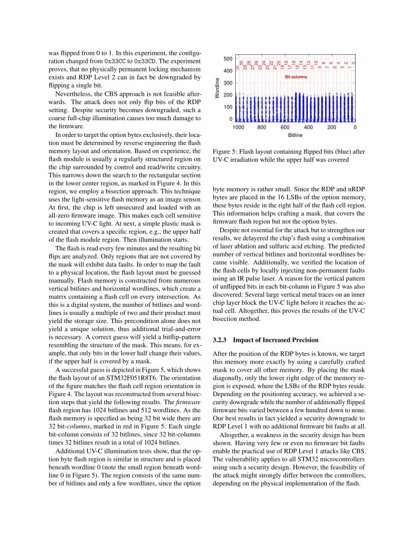
A successful guess is depicted in Figure 5, which showsthe flash layout of an STM32F051R8T6. The orientationof the figure matches the flash cell region orientation inFigure 4. The layout was reconstructed from several bisec-tion steps that yield the following results. The firmwareflash region has 1024 bitlines and 512 wordlines. As theflash memory is specified as being 32 bit wide there are32 bit-columns, marked in red in Figure 5. Each singlebit-column consists of 32 bitlines, since 32 bit-columnstimes 32 bitlines result in a total of 1024 bitlines.
Additional UV-C illumination tests show, that the op-tion byte flash region is similar in structure and is placedbeneath wordline 0 (note the small region beneath word-line 0 in Figure 5). The region consists of the same num-ber of bitlines and only a few wordlines, since the option
0
100
200
300
400
500
1000 800 600 400 200 0
Word
line
Bitline
313
02
92
82
72
62
52
42
32
22
12
01
91
81
71
61
51
41
31
21
11
0 9
8 7
6 5
4 3
2 1
0
Bit-columnsBit-columns
Figure 5: Flash layout containing flipped bits (blue) afterUV-C irradiation while the upper half was covered
byte memory is rather small. Since the RDP and nRDPbytes are placed in the 16 LSBs of the option memory,these bytes reside in the right half of the flash cell region.This information helps crafting a mask, that covers thefirmware flash region but not the option bytes.
Despite not essential for the attack but to strengthen ourresults, we delayered the chip’s flash using a combinationof laser ablation and sulfuric acid etching. The predictednumber of vertical bitlines and horizontal wordlines be-came visible. Additionally, we verified the location ofthe flash cells by locally injecting non-permanent faultsusing an IR pulse laser. A reason for the vertical patternof unflipped bits in each bit-column in Figure 5 was alsodiscovered: Several large vertical metal traces on an innerchip layer block the UV-C light before it reaches the ac-tual cell. Altogether, this proves the results of the UV-Cbisection method.
3.2.3 Impact of Increased Precision
After the position of the RDP bytes is known, we targetthis memory more exactly by using a carefully craftedmask to cover all other memory. By placing the maskdiagonally, only the lower right edge of the memory re-gion is exposed, where the LSBs of the RDP bytes reside.Depending on the positioning accuracy, we achieved a se-curity downgrade while the number of additionally flippedfirmware bits varied between a few hundred down to none.Our best results in fact yielded a security downgrade toRDP Level 1 with no additional firmware bit faults at all.
Altogether, a weakness in the security design has beenshown. Having very few or even no firmware bit faultsenable the practical use of RDP Level 1 attacks like CBS.The vulnerability applies to all STM32 microcontrollersusing such a security design. However, the feasibility ofthe attack might strongly differ between the controllers,depending on the physical implementation of the flash.

3.2.4 Countermeasure: RDP Downgrade Detection
There exists no countermeasure to prevent a securitydowngrade, since the issue persists in hardware. It isup to the manufacturer to enhance the concept, e.g., byusing RDP Level 2 instead of 1 as default/fallback setting.
Nevertheless, the effects of an attack can be mitigated.Upon startup, the firmware should immediately check,whether the expected level of protection is still active.This includes the “read protection level status” in theFLASH OBR register as well as the option bytes them-selves. In case of a mismatch between the setting and theexpectation, the RDP Level 2 setting should be rewrittento the option bytes, as this will restore missing charge inthe flash cells and re-enable security.
3.3 Debug Interface ExploitThe STM32F0 series microcontrollers do not have a JTAGinterface but use the Serial Wire Debug (SWD) interfacefor debugging and flash programming. When a debuggerbecomes attached to this interface in RDP Level 1, theflash protection logic cuts access to flash memory. Thissparsely documented mechanism raises interest and asksfor a thorough investigation.
3.3.1 Reverse Engineering
For the analysis, using the common off-the-shelf debug-ger ST-LINK fails. As soon as the debugger becomesconnected the flash is immediately locked down. Thisissue is caused by the debugger, which triggers the pro-tection mechanism by performing several SWD requestsautomatically upon connecting. As the immediate lockupprevents a precise analysis, this overly verbose debuggeris of no use for our experiment.
In order to gain control down to the physical layer ofSWD communication, we implement an own rudimentarybut versatile debugger. This is feasible, since the SWDinterface is well-documented [2]: SWD uses two signals,SWDIO and SWCLK, for synchronous communicationbetween the debugger and the microcontroller. SWDIOis a bidirectional data signal, SWCLK is the clock usedin the communication.
Figure 6 shows the wiring of our setup. The debug-ger (DBG) is controlled by the Laptop using a UART.The debugger is connected to the power, reset and SWDsignals of the microcontroller under analysis and attack.The associated firmware gives us full access to all SWDcommunication layers, thus, a detailed analysis becomespossible.
The first experiment tests, which SWD transactionstrigger the flash protection logic. Therefore, the systemis set to RDP Level 1, the firmware runs from flash andflashes an LED. The flashing LED shows, that the system
Device under A�ack
+3.3V
ResetSWDIOSWCLK
STM32µC
SWD FirmwareExtractor / DBG
TX
RXUSB UART AdapterLa
pto
p
USB
GNDPower
USB
Figure 6: Schematic of the SWD experiments and DebugInterface Exploitation
is running unperturbed. When flash access is blocked, theCPU fails to fetch any further instructions and the flashingof the LED stops.
The experiment shows, that the protection mechanismis not triggered by all SWD requests but only if a systembus (e.g., AHB-Lite [1]) is accessed. Accessing onlySWD interface-internal registers has no consequences andthe system remains running. But as soon as the debuggeruses the system bus to access any other module, such asperipherals, SRAM or flash, debug mode is entered andthe flash becomes locked down.
The debugger triggers a transfer on the system busby reading from or writing to the SWD AHB AccessPort (AHB-AP) Data Read/Write register. A closer analy-sis reveals, that the AHB transaction and therefore thelockdown is triggered by the last rising SWCLK edge ofthe corresponding SWD packet transmission.
3.3.2 Discovery and Analysis of the Vulnerability
In order to analyze the flash protection logic behavior,the amount of SWD communication is reduced to itsessentials. Most SWD requests are removed which leadsto a minimal configuration, where the SWD interfaceis fully initialized, but the flash protection has not beentriggered, yet. In the next step, a bus access is triggeredby a read request from a flash address. This is expectedto trigger the flash protection logic. This happens in fact—but in rare cases, some data ends up in the read buffer. Toour surprise, this is data from the actually read-protectedflash memory.
If at all, this deviation from the specification is observedonly on the first bus read access. Any subsequent readattempts always fail and return an SWD ERROR response.To repeat the experiment, the flash protection logic mustbe reset by a power-cycle.
The read access shows to be only randomly successful.As this is typical for a timing-based race condition, we tin-ker around with the bus load and timings to investigate thisissue further. Therefore we implement different firmwaresusing Assembly language, one containing mostly no-operations (NOPs) and another one featuring long se-

quences of store (STR) instructions. Altogether, the busload varies from roughly 50 % for the NOP firmware toup to 100 % for the STR firmware. The access succeedsin every case while running the NOP firmware, but theaccess always fails for the STR-sequences firmware. Thisshows that the issue is bus load related.
A look into the Cortex-M0 specification [3] supportsthe conjecture of a timing issue. CPU instruction and datafetches have priority over debug access during arbitration.Thus, the debugger has to wait for a free cycle on the busto place the request. If the debugger gains instant access tothe bus, the access takes place before the flash protectionlocking becomes triggered—thus, a typical race conditionoccurs. In the other case, when the debugger’s accessis delayed by an ongoing CPU access, the protectionlogic wins the race and the flash module will reject thedebugger’s later-arriving read attempt.
We investigate this further by linearly adding bus loadby increasing the number of wait states of the flash mod-ule. At zero wait states, a read access takes two cycles onthe AHB, one for the address phase and one for the dataphase [1]. Wait state cycles are inserted before the dataphase. Taking the NOP firmware as a basis, we observe,that adding one wait cycle will cause one out of three readaccesses to fail. By gradually increasing the wait states wup to the maximum of seven, we observed, that the readsuccess probability ps adheres to the following term:
ps = 1− w2+w
=2
2+w
The rearranged term at the right hand side of the equa-tion allows us to give an educated guess about the internaltiming issue. The denominator (2+w) represents the totalnumber of bus cycles for the AHB flash access. There-fore the numerator 2 is the number of vulnerable buscycles. Hence, we come to the conclusion, that the flashprotection logic is triggered two cycles too late.
By using the STR firmware we are able to show, thatthe flash module itself manages the access restrictions.The firmware rapidly toggles an LED using the bus, thusbus load will cause a measurable timing jitter. At a failedaccess to the flash, the bus is blocked for three clockcycles in total, which matches the duration of an errorresponse [1] on the AHB. Thus, the access is activelydenied by the flash module. Furthermore, this shows, thatthe protection logic makes the decision about the accessdirectly after the data phase as no wait states were everobserved during a failed access.
The reason for the protection delay of two clock cycleslies in the chip’s hardware design, but the exact locationremains unclear. One possible cause may be an incorrectimplementation of clock-domain crossing between thedebug clock domain [2] and the remaining logic.
Figure 7: Setup for PoCfirmware extraction out of a de-vice using RDP Level 1
Altogether, these experiments show, that there is a ma-jor hardware issue, that annuls the chip’s content protec-tion mechanism.
3.3.3 Proof-of-Concept: Code Extraction
This PoC demonstrates, that not only a single access canbe performed, but the whole firmware can be extractedfrom a microcontroller, using the aforementioned weak-ness. The setup is shown in Figure 7, which is the practi-cal realization of Figure 6. The Firmware Extractor readsout the firmware of the device under attack which is set toRDP Level 1. The PoC employs two STM32F0 Discoveryboards with STM32F051R8T6 microcontrollers.
In the PoC, the laptop controls the Firmware Extractorusing its UART interface. This interface configures pa-rameters, e.g., the read source address and the data lengthto be extracted. During readout, the data is sent to thelaptop using the UART interface.
The attack is implemented in a straightforward mannerwith one extension. As the read access works only oncebefore the system is locked up, the Firmware Extractorperforms a power cycle on the device under attack aftereach readout. Thus, the following steps are executed:
1. System Reset: Initially, a power cycle is applied toreset the system and flash protection logic.
2. Debugger interface initialization: The steps, de-scribed in the datasheets [15, 2], are followed. First,the SWD interface is reset by applying the resetpattern onto SWDIO and SWCLK. Secondly, thedebugger reads the IDCODE from the SWD De-bug Port (SWD-DP). Thirdly, the debugger sets theSystem power-up request (CSYSPWRUPREQ) andDebug power-up request (CDBGPWRUPREQ) inthe CTRL/STAT register of the SWD-DP to fullyinitialize the debug interface.

3. Set the access width to 32 bit: Although optional,switching into 32-bit mode is recommended, as afull word can be extracted in each step. Therefore,the size field in the AHB Access Port (AHB-AP)Control/Status Word Register has to be set to 0x02.
4. Set flash source address: The address to be read iswritten into the AHB-AP Transfer Address Register.
5. Trigger the flash read bus access: The debuggerperforms a read access from the AHB-AP DataRead/Write register. This triggers the AHB transac-tion that reads the flash memory.
6. Read the extracted data: The result of the previousaccess is read from the DP Read Buffer register. Onsuccess, if flash access was granted, an SWD OKresponse is returned. On failure, SWD ERROR isreturned. In the case of SWD OK, the word was cor-rectly extracted from flash and is sent to the Laptop.
7. Iterate: Upon success, this procedure is restartedwith (address+ 4), in order to read the next wordfrom flash. On failure, the address is not incrementedand the read access is retried.
The PoC was successfully tested on STM32F051R8T6and STM32F030R8T6. Due to the very similar chip func-tionality, we expect, that the whole STM32F0 series isaffected. Nevertheless, experiments on a few samplesindicate, that other series might not be vulnerable.
The PoC extracts firmware at 45 bytes per second onaverage. The largest STM32F0 microcontrollers with upto 256kByte of flash memory can be read out completelyin less than two hours, thus rendering the attack practicallyfeasible.
3.3.4 Consideration of Countermeasures
The attack can be aggravated by relinquishing the useof RDP Level 1 and setting the device to RDP Level 2,since this disables the debug interface. Nevertheless, thisdoes not fully resolve the issue, because the protectionlevel is non-permanent, as shown in Section 3.2. In com-parison to the CBS attack, the requirements put on thesecurity downgrade are significantly relaxed. While thefirmware must remain intact and executable for CBS, thedebug interface exploit works also on damaged firmware.Thus correctly placing the mask for the security down-grade is less demanding. Even if data errors occur, theyare usually limited to a small range of addresses, thusdestroying cryptographic material or other IP is ratherunlikely. Hence, there is no strong protection, especiallyif combined attacks are also considered.
4 Conclusion and Outlook
We presented three major security issues in the STM32F0series that leverage firmware content protection. Wewere able to develop all weaknesses to vulnerabilities bydemonstrating their practical exploitability. The demon-stration was conducted with the aid of three PoCs, one foreach vulnerability. They demonstrate the practical rele-vance of our work and present novel methods for attacksand reverse-engineering.
First, the readability of SRAM in RDP Level 1 emergesto a practical threat, as it often allows the reading of cryp-tographic material up to the whole firmware. Secondly,the stronger RDP Level 2 incorporates a design error,which significantly weakens the security concept and en-ables a security downgrade. Thirdly, the SWD hardwareimplementation contains a race-condition in RDP Level 1that completely annuls device security and exposes thefirmware to the attacker.
Altogether, these vulnerabilities completely break se-curity for RDP Level 1 and alarmingly weaken securityfor RDP Level 2. Since only low-cost lab equipment is re-quired, the impact increases. Especially the combinationof vulnerabilities, e.g., downgrading security from RDPLevel 2 and using the SWD exploit to read the firmwarepushes the complexity of attacks down to the hobbyist-level. Cold-Boot Stepping and the security downgrademight also work on other STM32 chip series, as they arebased on the same concept. Thus, the impact of this analy-sis is severe and might be expendable to more systems.
All in all, the presented results need to be taken intoconsideration when an STM32 microcontroller has to bedecently secured. We plan to extend our analysis to moresystems, to improve the attacks, and to dig deeper into theSTM32 internals.
5 Acknowledgments
The authors would like to thank Robert Specht and TolgaSel for preceding work concerning STM32 flash security.Special thanks to Michael Hani for supplying decommis-sioned but helpful lab equipment for our experiments.
6 Availability
We provide supplementary material under the MIT licenseat https://science.obermaier-johannes.de.
The material includes all required scripts, ELF, andsource code files for the Cold-Boot Stepping and DebugInterface Exploit PoCs, as well as sample firmware to beattacked.

References[1] ARM LIMITED. AMBA 3 AHB-Lite Protocol Specification v1.0,
2006.
[2] ARM LIMITED. CoreSight Components Technical ReferenceManual, 2009.
[3] ARM LIMITED. Cortex-M0 Technical Reference Manual, 2009.
[4] BAR-EL, H., CHOUKRI, H., NACCACHE, D., TUNSTALL, M.,AND WHELAN, C. The sorcerer’s apprentice guide to fault attacks.Proceedings of the IEEE 94, 2 (2006), 370–382.
[5] BEZ, R., CAMERLENGHI, E., MODELLI, A., AND VISCONTI,A. Introduction to flash memory. Proceedings of the IEEE 91, 4(2003), 489–502.
[6] HALDERMAN, J. A., SCHOEN, S. D., HENINGER, N., CLARK-SON, W., PAUL, W., CALANDRINO, J. A., FELDMAN, A. J.,APPELBAUM, J., AND FELTEN, E. W. Lest we remember: cold-boot attacks on encryption keys. Communications of the ACM 52,5 (2009), 91–98.
[7] IGNAT, V. Patent and product piracy. IOP Conference Series:Materials Science and Engineering 147, 1 (2016), 012105.
[8] KAHNG, D., AND SZE, S. M. A floating gate and its applicationto memory devices. The Bell System Technical Journal 46, 6 (July1967), 1288–1295.
[9] KOTHANDARAMAN, C., IYER, S. K., AND IYER, S. S. Elec-trically programmable fuse (efuse) using electromigration in sili-cides. IEEE Electron Device Letters 23, 9 (Sept 2002), 523–525.
[10] OBERMAIER, J. OpenOCD Patch: flash/nor/stm32f1x: AddedRDP Level 2 support. http://openocd.zylin.com/4111,2017. [Accessed 01-May-2017].
[11] SKOROBOGATOV, S. Flash memory ‘bumping’attacks. In Inter-national Workshop on Cryptographic Hardware and EmbeddedSystems (2010), Springer, pp. 158–172.
[12] SKOROBOGATOV, S., AND WOODS, C. Breakthrough SiliconScanning Discovers Backdoor in Military Chip. Springer BerlinHeidelberg, Berlin, Heidelberg, 2012, pp. 23–40.
[13] SKOROBOGATOV, S. P., AND ANDERSON, R. J. Optical faultinduction attacks. In International workshop on cryptographichardware and embedded systems (2002), Springer, pp. 2–12.
[14] STMICROELECTRONICS. Datasheet STM32F303xBSTM32F303xC, May 2016. Rev 13.
[15] STMICROELECTRONICS. RM0091 Reference manual,STM32F0x1/ STM32F0x2/ STM32F0x8 advanced ARM R©-based32-bit MCUs, January 2017. Rev. 9.
[16] STROBEL, D., DRIESSEN, B., KASPER, T., LEANDER, G., OS-WALD, D., SCHELLENBERG, F., AND PAAR, C. Fuming Acid andCryptanalysis: Handy Tools for Overcoming a Digital Lockingand Access Control System. Springer Berlin Heidelberg, Berlin,Heidelberg, 2013, pp. 147–164.
[17] VARIOUS AUTHORS. Mikrocontroller.net: Meteotime Crypt.https://www.mikrocontroller.net/topic/220947, 2011.[In German; accessed 01-May-2017].
[18] WARREN, H. S. Hacker’s delight. Pearson Education, 2013.