si5391 reference manual - silabs.com · this reference manual is to be used to describe all the...
TRANSCRIPT

Si5391 Reference Manual
Ultra Low Jitter, Any-Frequency, Any Output Clock Generator:Si5391 Reference ManualThe Si5391 Clock Generators combine MultiSynth™ technologies to enable any-fre-quency clock generation for applications that require the highest level of jitter perform-ance. These devices are programmable via a serial interface with in-circuit programma-ble nonvolatile memory (NVM) ensuring power up with a known frequency configura-tion.
RELATED DOCUMENTS
• Si5391 Data Sheet• Si5391 Device Errata• Si5391-EVB User Guide• Si5391-EVB Schematics, BOM & Layout• IBIS models
silabs.com | Building a more connected world. Rev. 0.2
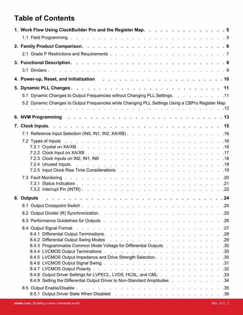
Table of Contents1. Work Flow Using ClockBuilder Pro and the Register Map. . . . . . . . . . . . . . . 5
1.1 Field Programming . . . . . . . . . . . . . . . . . . . . . . . . . . . . 5
2. Family Product Comparison. . . . . . . . . . . . . . . . . . . . . . . . . . 62.1 Grade P Restrictions and Requirements . . . . . . . . . . . . . . . . . . . . . 7
3. Functional Description. . . . . . . . . . . . . . . . . . . . . . . . . . . . 83.1 Dividers . . . . . . . . . . . . . . . . . . . . . . . . . . . . . . . . 9
4. Power-up, Reset, and Initialization . . . . . . . . . . . . . . . . . . . . . . 10
5. Dynamic PLL Changes . . . . . . . . . . . . . . . . . . . . . . . . . . . 115.1 Dynamic Changes to Output Frequencies without Changing PLL Settings. . . . . . . . . .11
5.2 Dynamic Changes to Output Frequencies while Changing PLL Settings Using a CBPro Register Map. . . . . . . . . . . . . . . . . . . . . . . . . . . . . . . . . . .12
6. NVM Programming . . . . . . . . . . . . . . . . . . . . . . . . . . . . 13
7. Clock Inputs. . . . . . . . . . . . . . . . . . . . . . . . . . . . . . . 157.1 Reference Input Selection (IN0, IN1, IN2, XA/XB) . . . . . . . . . . . . . . . . . .16
7.2 Types of Inputs . . . . . . . . . . . . . . . . . . . . . . . . . . . . .167.2.1 Crystal on XA/XB. . . . . . . . . . . . . . . . . . . . . . . . . . .167.2.2 Clock Input on XA/XB . . . . . . . . . . . . . . . . . . . . . . . . .177.2.3 Clock Inputs on IN2, IN1, IN0 . . . . . . . . . . . . . . . . . . . . . .187.2.4 Unused Inputs. . . . . . . . . . . . . . . . . . . . . . . . . . . .187.2.5 Input Clock Rise Time Considerations. . . . . . . . . . . . . . . . . . . .19
7.3 Fault Monitoring . . . . . . . . . . . . . . . . . . . . . . . . . . . . .207.3.1 Status Indicators . . . . . . . . . . . . . . . . . . . . . . . . . . .217.3.2 Interrupt Pin (INTR) . . . . . . . . . . . . . . . . . . . . . . . . . .22
8. Outputs . . . . . . . . . . . . . . . . . . . . . . . . . . . . . . . . 248.1 Output Crosspoint Switch . . . . . . . . . . . . . . . . . . . . . . . . . .24
8.2 Output Divider (R) Synchronization . . . . . . . . . . . . . . . . . . . . . . .25
8.3 Performance Guidelines for Outputs . . . . . . . . . . . . . . . . . . . . . .26
8.4 Output Signal Format . . . . . . . . . . . . . . . . . . . . . . . . . . .278.4.1 Differential Output Terminations. . . . . . . . . . . . . . . . . . . . . .288.4.2 Differential Output Swing Modes . . . . . . . . . . . . . . . . . . . . .298.4.3 Programmable Common Mode Voltage for Differential Outputs . . . . . . . . . . .308.4.4 LVCMOS Output Terminations . . . . . . . . . . . . . . . . . . . . . .308.4.5 LVCMOS Output Impedance and Drive Strength Selection. . . . . . . . . . . . .308.4.6 LVCMOS Output Signal Swing . . . . . . . . . . . . . . . . . . . . . .318.4.7 LVCMOS Output Polarity . . . . . . . . . . . . . . . . . . . . . . . .328.4.8 Output Driver Settings for LVPECL, LVDS, HCSL, and CML . . . . . . . . . . . .338.4.9 Setting the Differential Output Driver to Non-Standard Amplitudes . . . . . . . . . .34
8.5 Output Enable/Disable . . . . . . . . . . . . . . . . . . . . . . . . . . .358.5.1 Output Driver State When Disabled . . . . . . . . . . . . . . . . . . . .36
silabs.com | Building a more connected world. Rev. 0.2 | 2

8.5.2 Synchronous Output Enable/Disable Feature . . . . . . . . . . . . . . . . .37
8.6 Output Buffer Supply Voltage Selection . . . . . . . . . . . . . . . . . . . . .37
8.7 Output Delay Control (Δt0 – Δt4) . . . . . . . . . . . . . . . . . . . . . . . .38
9. Zero Delay Mode (All Si5391 Devices Except Si5391P) . . . . . . . . . . . . . . . 39
10. Digitally-Controlled Oscillator (DCO) Mode (All Si5391 Devices Except Si5391P) . . . .4110.1 Using the N Dividers for DCO Applications . . . . . . . . . . . . . . . . . . . .41
10.1.1 DCO with Frequency Increment/Decrement Pins/Bits . . . . . . . . . . . . . .4110.1.2 DCO with Direct Register Writes . . . . . . . . . . . . . . . . . . . . .41
10.2 Using the M Divider for DCO Applications . . . . . . . . . . . . . . . . . . . .41
11. Serial Interface . . . . . . . . . . . . . . . . . . . . . . . . . . . . . 42
11.1 I2C Interface . . . . . . . . . . . . . . . . . . . . . . . . . . . . . .44
11.2 SPI Interface . . . . . . . . . . . . . . . . . . . . . . . . . . . . . .46
12. XAXB External References . . . . . . . . . . . . . . . . . . . . . . . . . 5112.1 Performance of External References . . . . . . . . . . . . . . . . . . . . . .51
12.2 Recommend Crystals and Oscillators . . . . . . . . . . . . . . . . . . . . .52
12.3 Register Settings to Configure for External XTAL Reference . . . . . . . . . . . . . .5212.3.1 XAXB_EXTCLK_EN Reference Clock Selection Register . . . . . . . . . . . . .5212.3.2 PXAXB Pre-scale Divide Ratio for Reference Clock Register . . . . . . . . . . .52
13. Crystal and Device Circuit Layout Recommendations . . . . . . . . . . . . . .5313.1 64-Pin QFN Si5391 Layout Recommendations . . . . . . . . . . . . . . . . . .53
13.1.1 Si5391 with an External Reference (Not Relevant to the Si5391P) . . . . . . . . .5313.1.2 Si5391 Crystal Guidelines . . . . . . . . . . . . . . . . . . . . . . .5413.1.3 Si5391 Output Clocks . . . . . . . . . . . . . . . . . . . . . . . . .60
14. Power Management . . . . . . . . . . . . . . . . . . . . . . . . . . . 6214.1 Power Management Features . . . . . . . . . . . . . . . . . . . . . . . .62
14.2 Power Supply Recommendations . . . . . . . . . . . . . . . . . . . . . . .62
14.3 Power Supply Sequencing . . . . . . . . . . . . . . . . . . . . . . . . .63
14.4 Grounding Vias . . . . . . . . . . . . . . . . . . . . . . . . . . . . .63
15. Register Map . . . . . . . . . . . . . . . . . . . . . . . . . . . . . . 6415.1 Base vs. Factory Preprogrammed Devices. . . . . . . . . . . . . . . . . . . .64
15.2 “Base” Devices (a.k.a. “Blank” Devices) . . . . . . . . . . . . . . . . . . . . .64
15.3 “Factory Preprogrammed” (Custom OPN) Devices . . . . . . . . . . . . . . . . .64
15.4 Register Map Overview and Default Settings Values . . . . . . . . . . . . . . . .65
16. Si5391A/B Register Map . . . . . . . . . . . . . . . . . . . . . . . . . . 6616.1 Page 0 Registers Si5391. . . . . . . . . . . . . . . . . . . . . . . . . .66
16.2 Page 1 Registers Si5391. . . . . . . . . . . . . . . . . . . . . . . . . .75
16.3 Page 2 Registers Si5391. . . . . . . . . . . . . . . . . . . . . . . . . .79
silabs.com | Building a more connected world. Rev. 0.2 | 3

16.4 Page 3 Registers Si5391. . . . . . . . . . . . . . . . . . . . . . . . . .85
16.5 Page 9 Registers Si5391. . . . . . . . . . . . . . . . . . . . . . . . . .89
16.6 Page A Registers Si5391 . . . . . . . . . . . . . . . . . . . . . . . . .90
16.7 Page B Registers Si5391 . . . . . . . . . . . . . . . . . . . . . . . . .90
17. Revision History. . . . . . . . . . . . . . . . . . . . . . . . . . . . . 92
silabs.com | Building a more connected world. Rev. 0.2 | 4

1. Work Flow Using ClockBuilder Pro and the Register Map
This reference manual is to be used to describe all the functions and features of the parts in the product family with register map detailson how to implement them. It is important to understand that the intent is for customers to use the ClockBuilder Pro software to providethe initial configuration for the device. Although the register map is documented, all the details of the algorithms to implement a validfrequency plan are fairly complex and are beyond the scope of this document. Real-time changes to the frequency plan and other oper-ating settings are supported by the devices. However, describing all the possible changes is not a primary purpose of this document.Refer to the applications notes and Knowledge Base articles within the ClockBuilder Pro GUI for information on how to implement themost common, real-time frequency plan changes.
The primary purpose of the software is to enable use of the device without an in-depth understanding of its complexities. The softwareabstracts the details from the user to allow focus on the high level input and output configuration, making it intuitive to understand andconfigure for the end application. The software walks the user through each step, with explanations about each configuration step in theprocess to explain the different options available. The software will restrict the user from entering an invalid combination of selections.The final configuration settings can be saved, written to an EVB and a custom part number can be created for customers who prefer toorder a factory preprogrammed device. The final register maps can be exported to text files, and comparisons can be done by viewingthe settings in the register map described in this document.
1.1 Field Programming
To simplify design and software development of systems using the Si5391/Si5391P, a field programmer is available in addition to theevaluation board. The ClockBuilder Pro Field Programmer supports both “in-system” programming (for devices already mounted on aPCB), as well as “in-socket” programming of Si5391/Si5391P sample devices. Refer to www.silabs.com/CBProgrammer for informationabout this kit.
Si5391 Reference ManualWork Flow Using ClockBuilder Pro and the Register Map
silabs.com | Building a more connected world. Rev. 0.2 | 5

2. Family Product Comparison
The following table is a comparison of the different parts in the product family showing the differences in the inputs, MultiSynths, out-puts and package type.
Table 2.1. Family Feature Comparison
Part Number Number of Inputs Number of Fractional Dividers Number of Outputs Package Type
Si5391 4 5 12 64-pin QFN
VDD
VDD
A
3
SDA/ SDIOA1/SDO
SCLK
A0/CSb
I2C_SEL
SPI /I2C NVM
RSTb
Zero Delay Mode
FB_INFB_INb
OEb
Si5391Generator
Clock
÷R0
÷R2
÷R3
÷R4
÷R5
÷R6
÷R7
÷R8
÷R9
÷R1
OUT0b
VDDO0OUT0
OUT2b
VDDO2OUT2
OUT3b
VDDO3OUT3
OUT4b
VDDO4OUT4
OUT5b
VDDO5OUT5
OUT6b
VDDO6OUT6
OUT7b
VDDO7OUT7
OUT8b
VDDO8OUT8
OUT9b
VDDO9OUT9
OUT1b
VDDO1OUT1
÷Pfb
LPF
PD
÷Mn
Md
PLL
IN_SEL[1:0]
XA
XB
÷P2
÷P1
÷P0IN0
IN0b
IN1IN1b
IN2IN2b
FDEC
FIN
C
Frequency Control
÷ N0nN0d
t0
÷ N2nN2d
÷ N3nN3d
÷ N4nN4d
t2
t3
t4
÷ N1nN1d
t1
MultiSynth
SYNC
b
Dividers/Drivers
StatusMonitors
LOLb
INTR
b
OSC
÷ PXAXB
25-54 MHzXTAL
÷R9A OUT9AbOUT9A
÷R0A OUT0AbOUT0A
Si5391P: 48 MHz only
Figure 2.1. Block Diagram Si5391/Si5391P
Si5391 Reference ManualFamily Product Comparison
silabs.com | Building a more connected world. Rev. 0.2 | 6

2.1 Grade P Restrictions and Requirements
Some applications like 56G PAM4 SERDES require even higher performance than is already provided by standard clock generators.The Si5391P grade internally calibrates out linearity errors to deliver the world's best jitter performance for applications focused on156.25 MHz and 312.5 MHz frequencies. For the Si5391P, the allowed output frequencies are restricted to the following: 25 MHz, 50MHz, 100 MHz, 125 MHz, 156.25 MHz, or 312.5 MHz. Additionally, outputs that are assigned as either 156.25 MHz or 312.5 MHz canbe adjacent, but an "Unused" output must be assigned between any of 156.25 MHz or 312.5 MHz outputs and outputs using any of theother supported frequencies of 25/50/100/125 MHz. These rules are enforced by Clock Builder Pro.
In additon, grade 'P' part XTAL frequency is fixed at 48 MHz and variation must be within ±100 ppm across temperature and aging.
Si5391 Reference ManualFamily Product Comparison
silabs.com | Building a more connected world. Rev. 0.2 | 7

3. Functional Description
The Si5391 uses next generation MultiSynth™ technology to offer the industry’s most frequency-flexible, high performance clock gener-ator. The internal Phase-Locked Loop (PLL) locks to either an external crystal (XA/XB) or to an external input on XAXB, IN0, IN1 or IN2.The input frequency (crystal or external input) is multiplied by the PLL and divided by the MultiSynth™ stage (N divider) and R divider toany frequency in the range of 100 Hz to 712.5 MHz per output. The PLL is fully contained and does not require external loop filtercomponents to operate. Its function is to phase lock to the selected input and provide a common reference to all the output MultiSynthhighperformance fractional dividers (N dividers). The high-resolution fractional MultiSynth™ dividers enables true any-frequency inputto any-frequency output. A cross-point mux connects any of the MultiSynth divided frequencies to any of the output drivers. Additionalinteger output dividers (R) provide further frequency division if required. The frequency configuration of the device is programmed bysetting the input dividers (P), the PLL feedback fractional divider (M_NUM/M_DEN), the MultiSynth fractional dividers (N_NUM/N_DEN), and the output integer dividers (R). Silicon Labs’ Clockbuilder Pro configuration utility determines the optimum divider valuesfor any desired input and output frequency plan.
The output drivers offer flexible output formats which are independently configurable on each of the outputs. This clock generator is fullyconfigurable via its serial interface (I2C/SPI) and includes in-circuit programmable non-volatile memory. The block diagram for theSi5391 is shown in the figure below.
VDD
VDD
A
3
SDA/ SDIOA1/SDO
SCLK
A0/CSb
I2C_SEL
SPI /I2C NVM
RSTb
Zero Delay Mode
FB_INFB_INb
OEb
Si5391Generator
Clock
÷R0
÷R2
÷R3
÷R4
÷R5
÷R6
÷R7
÷R8
÷R9
÷R1
OUT0b
VDDO0OUT0
OUT2b
VDDO2OUT2
OUT3b
VDDO3OUT3
OUT4b
VDDO4OUT4
OUT5b
VDDO5OUT5
OUT6b
VDDO6OUT6
OUT7b
VDDO7OUT7
OUT8b
VDDO8OUT8
OUT9b
VDDO9OUT9
OUT1b
VDDO1OUT1
÷Pfb
LPF
PD
÷Mn
Md
PLL
IN_SEL[1:0]
XA
XB
÷P2
÷P1
÷P0IN0
IN0b
IN1IN1b
IN2IN2b
FDEC
FIN
C
Frequency Control
÷ N0nN0d
t0
÷ N2nN2d
÷ N3nN3d
÷ N4nN4d
t2
t3
t4
÷ N1nN1d
t1
MultiSynth
SYNC
b
Dividers/Drivers
StatusMonitors
LOLb
INTR
b
OSC
÷ PXAXB
25-54 MHzXTAL
÷R9A OUT9AbOUT9A
÷R0A OUT0AbOUT0A
Si5391P: 48 MHz only
Figure 3.1. Si5391 Block Diagram
Si5391 Reference ManualFunctional Description
silabs.com | Building a more connected world. Rev. 0.2 | 8

3.1 Dividers
There are five main divider classes within the Si5391/Si5391P shown above in the Figure 3.1 Si5391 Block Diagram on page 8.1. Wide range input dividers Pfb, P2, P1, P0
• Only integer divider values• Range is from 1 to 216 – 1• Since the input to the phase detector needs to be > 10 MHz, the practical range is limited to ~75 on the high side.• Each divider has an update bit that must be written to cause a newly written divider value to take effect.
2. Narrow range input divider Pxaxb• Only divides by 1, 2, 4, 8
3. Feedback M divider• Ultra low jitter in fractional and integer modes• MultiSynth divider• Integer or fractional divide values• 44 bit numerator, 32 bit denominator• Practical range limited by phase detector range of 10–120 MHz and VCO range of 13500–14256 MHz• This divider has an update bit that must be written to cause a newly written divider value to take effect.
4. Output N dividers• Ultra low jitter in fractional and integer modes• MultiSynth divider• Integer or fractional divide values• 44 bit numerator, 32 bit denominator• Min value is 10• Maximum value is 212 – 1• Each N divider has an update bit that must be written to cause a newly written divider value to take effect. In addition there is a
global update bit that when written updates all N dividers.5. Output R divider
• Only even integer divide values• Min value is 2• Maximum value is 225 – 2
Additionally, FSTEPW can be used to adjust the nominal output frequency in DCO mode. See Section 10. Digitally-Controlled Oscillator(DCO) Mode (All Si5391 Devices Except Si5391P) for more information and block diagrams on DCO mode.
Si5391 Reference ManualFunctional Description
silabs.com | Building a more connected world. Rev. 0.2 | 9
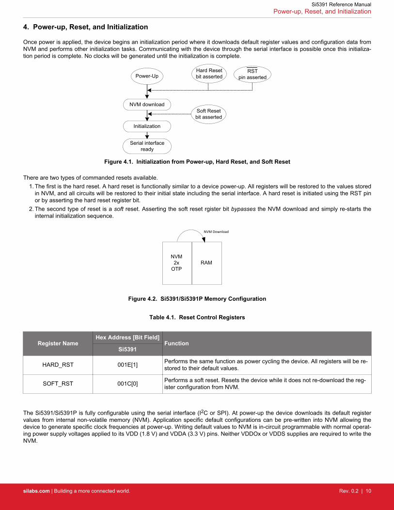
4. Power-up, Reset, and Initialization
Once power is applied, the device begins an initialization period where it downloads default register values and configuration data fromNVM and performs other initialization tasks. Communicating with the device through the serial interface is possible once this initializa-tion period is complete. No clocks will be generated until the initialization is complete.
Power-Up
Serial interface ready
RST pin asserted
Hard Reset bit asserted
Initialization
NVM downloadSoft Reset bit asserted
Figure 4.1. Initialization from Power-up, Hard Reset, and Soft Reset
There are two types of commanded resets available.1. The first is the hard reset. A hard reset is functionally similar to a device power-up. All registers will be restored to the values stored
in NVM, and all circuits will be restored to their initial state including the serial interface. A hard reset is initiated using the RST pinor by asserting the hard reset register bit.
2. The second type of reset is a soft reset. Asserting the soft reset rgister bit bypasses the NVM download and simply re-starts theinternal initialization sequence.
NVM2x
OTPRAM
NVM Download
Figure 4.2. Si5391/Si5391P Memory Configuration
Table 4.1. Reset Control Registers
Register NameHex Address [Bit Field]
FunctionSi5391
HARD_RST 001E[1] Performs the same function as power cycling the device. All registers will be re-stored to their default values.
SOFT_RST 001C[0] Performs a soft reset. Resets the device while it does not re-download the reg-ister configuration from NVM.
The Si5391/Si5391P is fully configurable using the serial interface (I2C or SPI). At power-up the device downloads its default registervalues from internal non-volatile memory (NVM). Application specific default configurations can be pre-written into NVM allowing thedevice to generate specific clock frequencies at power-up. Writing default values to NVM is in-circuit programmable with normal operat-ing power supply voltages applied to its VDD (1.8 V) and VDDA (3.3 V) pins. Neither VDDOx or VDDS supplies are required to write theNVM.
Si5391 Reference ManualPower-up, Reset, and Initialization
silabs.com | Building a more connected world. Rev. 0.2 | 10
5. Dynamic PLL Changes
It is possible for the PLL to become unresponsive (i.e., lose lock indefinitely) when it is dynamically reprogrammed or changed via theserial port. Any change that causes the VCO frequency to change by more than 250 ppm since Power-up, a NVM download, assertionof SOFT_RST, or changes to any of the following list of registers will require the special PLL re-initialization sequence below
Registers:
• XAXB_FREQ_OFFSET• PXAXB• MXAXB_NUM• MXAXB_DEN• M_NUM• M_DEN
PLL Re-Initialization Sequence:
1. First, the preamble:
Write 0x0B24 = 0xD8
Write 0x0B25 = 0x00
Write 0x0502 = 0x01
Write 0x0505 = 0x03
Write 0x0957 = 0x17
Write 0x0B4E = 0x1A2. Wait 300 ms.3. Then, perform the desired register modifications.4. Write SOFT_RST - 0x001C[0] = 15. Write the post-amble:
Write 0x0B24 = 0xDB
Write 0x0B25 = 0x02
Note: This programming sequence applies only to Rev D and later revisions. The preamble and postamble values for updating certainregisters during device operation are different for earlier revisions. Either the new or old values below may be written to revision D orlater devices without issue. No system software changes are necessary for legacy systems. When writing old values, note that readingback these registers will not give the written old values, but will reflect the new values. Silicon Labs recommends using the new valuesfor all revision D (described above) and later designs, since the write and read values will match. Please contact Silicon Labs if youneed information about an earlier revision. Please always ensure to use the correct sequence for the correct revision of the device. Alsocheck for the latest information online. This information is updated from time to time. The latest information is always posted online.
5.1 Dynamic Changes to Output Frequencies without Changing PLL Settings
This section applies to the following scenario:1. A CBPro generated register map "was" used to program either the volatile or the non-volatile memory of a Si5391. Changes to
output frequencies without changing the PLL settings are desired.2. The CBPro project file can be used to look for the VCO frequency (FVCO), Ry, Nx values for each OUTy in the design report
and/or the datasheet addendum.
OUTy = FVCO/(Nx * Ry)
Solve for Nx based on the desired OUTy. The Nx dividers can be digitally controlled to so that all outputs connected to the Nx dividerchange frequency in real time without any transition glitches. There are two ways to control the Nx divider to accomplish this task:
1. Use the Frequency Increment/Decrement Pins or register bits.2. Write directly to the numerator or denominator of the Nx divider.
The details of both methods are covered in 10.1 Using the N Dividers for DCO Applications.
Si5391 Reference ManualDynamic PLL Changes
silabs.com | Building a more connected world. Rev. 0.2 | 11
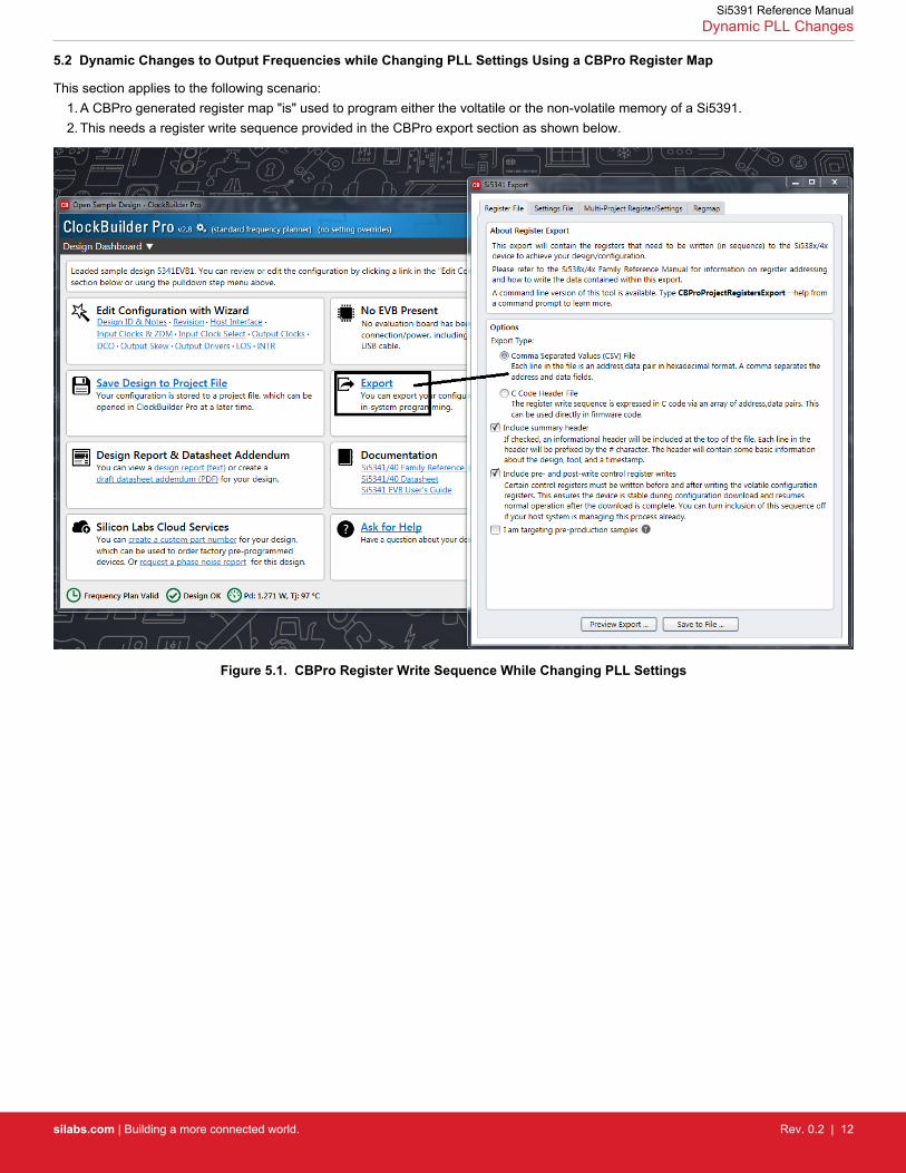
5.2 Dynamic Changes to Output Frequencies while Changing PLL Settings Using a CBPro Register Map
This section applies to the following scenario:1. A CBPro generated register map "is" used to program either the voltatile or the non-volatile memory of a Si5391.2. This needs a register write sequence provided in the CBPro export section as shown below.
Figure 5.1. CBPro Register Write Sequence While Changing PLL Settings
Si5391 Reference ManualDynamic PLL Changes
silabs.com | Building a more connected world. Rev. 0.2 | 12
6. NVM Programming
Devices have two categories of non-volatile memory: user NVM and Factory (Silabs) NVM. Each type is segmented into NVM banks.There are three NVM banks, one of which is used for factory programming (whether a base part or an Orderable Part Number). Twouser NVM banks remain; therefore, the device NVM can be re-burned in the field up to two times. Factory NVM cannot be modified, andcontains fixed configuration information for the device.
The ACTIVE_NVM_BANK device setting can be used to determine which user NVM bank is currently being used and therefore howmany banks, if any, are available to burn. The following table describes possible values:
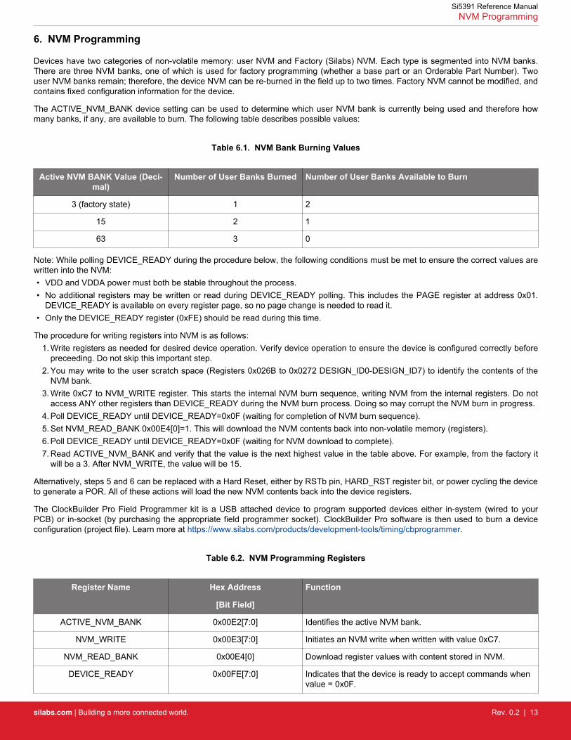
Table 6.1. NVM Bank Burning Values
Active NVM BANK Value (Deci-mal)
Number of User Banks Burned Number of User Banks Available to Burn
3 (factory state) 1 2
15 2 1
63 3 0
Note: While polling DEVICE_READY during the procedure below, the following conditions must be met to ensure the correct values arewritten into the NVM:• VDD and VDDA power must both be stable throughout the process.• No additional registers may be written or read during DEVICE_READY polling. This includes the PAGE register at address 0x01.
DEVICE_READY is available on every register page, so no page change is needed to read it.• Only the DEVICE_READY register (0xFE) should be read during this time.
The procedure for writing registers into NVM is as follows:1. Write registers as needed for desired device operation. Verify device operation to ensure the device is configured correctly before
preceeding. Do not skip this important step.2. You may write to the user scratch space (Registers 0x026B to 0x0272 DESIGN_ID0-DESIGN_ID7) to identify the contents of the
NVM bank.3. Write 0xC7 to NVM_WRITE register. This starts the internal NVM burn sequence, writing NVM from the internal registers. Do not
access ANY other registers than DEVICE_READY during the NVM burn process. Doing so may corrupt the NVM burn in progress.4. Poll DEVICE_READY until DEVICE_READY=0x0F (waiting for completion of NVM burn sequence).5. Set NVM_READ_BANK 0x00E4[0]=1. This will download the NVM contents back into non-volatile memory (registers).6. Poll DEVICE_READY until DEVICE_READY=0x0F (waiting for NVM download to complete).7. Read ACTIVE_NVM_BANK and verify that the value is the next highest value in the table above. For example, from the factory it
will be a 3. After NVM_WRITE, the value will be 15.
Alternatively, steps 5 and 6 can be replaced with a Hard Reset, either by RSTb pin, HARD_RST register bit, or power cycling the deviceto generate a POR. All of these actions will load the new NVM contents back into the device registers.
The ClockBuilder Pro Field Programmer kit is a USB attached device to program supported devices either in-system (wired to yourPCB) or in-socket (by purchasing the appropriate field programmer socket). ClockBuilder Pro software is then used to burn a deviceconfiguration (project file). Learn more at https://www.silabs.com/products/development-tools/timing/cbprogrammer.
Table 6.2. NVM Programming Registers
Register Name Hex Address
[Bit Field]
Function
ACTIVE_NVM_BANK 0x00E2[7:0] Identifies the active NVM bank.
NVM_WRITE 0x00E3[7:0] Initiates an NVM write when written with value 0xC7.
NVM_READ_BANK 0x00E4[0] Download register values with content stored in NVM.
DEVICE_READY 0x00FE[7:0] Indicates that the device is ready to accept commands whenvalue = 0x0F.
Si5391 Reference ManualNVM Programming
silabs.com | Building a more connected world. Rev. 0.2 | 13

Warning: Any attempt to read or write any register other than DEVICE_READY before DEVICE_READY reads as 0x0F may corruptthe NVM programming and may corrupt the register contents, as they are read from NVM. Note that this includes accesses to thePAGE register.
Si5391 Reference ManualNVM Programming
silabs.com | Building a more connected world. Rev. 0.2 | 14

7. Clock Inputs
Clock inputs can be used on all Si5391 grades except for Si5391P. The PLL in the Si5391 (not P grade) requires a clock input at theXAXB pins or IN2, 1, 0 input pins or a clock from a crystal connected across the XAXB pins. The PLL of the Si5391P requires a 48 MHzcrystal, not input clock, connected at the XAXB pins and does not use the IN0, 1, 2 inputs.
VDD
VDD
A
3
SDA/ SDIOA1/SDO
SCLK
A0/CSb
I2C_SEL
SPI /I2C NVM
RSTb
Zero Delay Mode
FB_INFB_INb
OEb
Si5391Generator
Clock
÷R0
÷R2
÷R3
÷R4
÷R5
÷R6
÷R7
÷R8
÷R9
÷R1
OUT0b
VDDO0OUT0
OUT2b
VDDO2OUT2
OUT3b
VDDO3OUT3
OUT4b
VDDO4OUT4
OUT5b
VDDO5OUT5
OUT6b
VDDO6OUT6
OUT7b
VDDO7OUT7
OUT8b
VDDO8OUT8
OUT9b
VDDO9OUT9
OUT1b
VDDO1OUT1
÷Pfb
LPF
PD
÷Mn
Md
PLL
IN_SEL[1:0]
XA
XB
÷P2
÷P1
÷P0IN0
IN0b
IN1IN1b
IN2IN2b
FDEC
FIN
C
Frequency Control
÷ N0nN0d
t0
÷ N2nN2d
÷ N3nN3d
÷ N4nN4d
t2
t3
t4
÷ N1nN1d
t1
MultiSynth
SYNC
b
Dividers/Drivers
StatusMonitors
LOLb
INTR
b
OSC
÷ PXAXB
25-54 MHzXTAL
÷R9A OUT9AbOUT9A
÷R0A OUT0AbOUT0A
Si5391P: 48 MHz only
Figure 7.1. Clock Inputs Example
Si5391 Reference ManualClock Inputs
silabs.com | Building a more connected world. Rev. 0.2 | 15

7.1 Reference Input Selection (IN0, IN1, IN2, XA/XB)
The active clock input is selected using the IN_SEL1,0 pins or by register control. The register bit IN_SEL_REGCTRL determines inputselection as pin or register selectable.
Note: If the selected input does not have a clock, all output clocks will be shut off (squelched) until a valid input clock is present.
Table 7.1. Manual Input Selection Using IN_SEL[1:0] Pins
IN_SEL[1:0] Selected Input
0 0 IN0
0 1 IN1
1 0 IN2
1 1 XA/XB
Table 7.2. Input Control Registers
Register NameHex Address [Bit Field]
FunctionSi5391
XAXB_FREQ_OFFSET1 0202[7:0]–0205[7:0]Note:
1. Do NOT use this register on any version of the Si5391.
XAXB_EXTCLK_EN 090E[0] Selects between the XTAL or external REFCLK on the XA/XBpins
IN_SEL_REGCTRL 0021[0] Determines pin or register clock input selection.
IN_SEL 0021[2:1] Selects the input when in register input selection mode.
IN_EN 0949[3:0] Allows enabling/disabling IN0, IN1, IN2 and FB_IN when not inuse.
7.2 Types of Inputs
7.2.1 Crystal on XA/XB
An external standard crystal (XTAL) is connected to XA/XB when this input is configured as a crystal oscillator. For all Si5391 devices,except the Si5391P, a crystal frequency of 25 MHz can be used, although crystals in the frequency range of 48 MHz to 54 MHz arehighly recommended for the best jitter performance. All Si5391 devices, except Si5391P, include a built-in XTAL load capacitance (CL)of 8 pF, but crystals with CL specifications as high as 18 pF can also be used. When using crystals with CL specs higher than 8 pf it isnot generally recommended to use external capacitors from XA/XB to ground to increase the crystal load capacitance. See Section13. Crystal and Device Circuit Layout Recommendations for the PCB layout guidelines.
For Si5391P devices, the crystal frequency MUST be 48 MHz and have a loading capacitance of 8 pf. No external loading capacitorsare needed since the device has a built-in loading capacitance of 8 pf.
Si5391 Reference ManualClock Inputs
silabs.com | Building a more connected world. Rev. 0.2 | 16

7.2.2 Clock Input on XA/XB
This section applies to all Si5391 devices except the Si5391P. The Si5391P must use a crystal on XAXB, not a clock.
An external clock can also be input on the XA/XB pins of all Si5391 devices except the Si5391P. Selection between the external crystalor clock is controlled by register configuration. The internal crystal load capacitors (CL) are disabled in external clock mode. Becausethe input buffer at XA/XB is a lower noise buffer than the buffers on IN2,1,0, a very clean input clock at XA/XB, such as a very highquality TCXO or XO, will, in some cases, produce lower output clock jitter than the same input at IN2,1,0. If the XAXB input is unusedand powered down then the XA and XB inputs can be left floating. Note that ClockBuilder Pro will power down the XAXB input if it isselected as “unused”. If XAXB is powered up but no input is applied then the XA input should be left floating and the XB input must beconnected directly to ground. Both a single-ended or a differential clock can be connected to the XA/XB pins as shown in the followingfigure:
50
Differential Connection
2xCL
2xCL
XB
XA
2xCL
2xCL
XB
XA
Single-ended XO Connection
Crystal Connection
OSC
XB
XA
XTAL
2xCL
2xCL
Si5391
Si5391 Si5391
Note: 2.0 Vpp_se max
XO with Clipped Sine Wave Output
2xCL
2xCL
XB
XAOSC
Si5391
Note: 2.0 Vpp_se maxCMOS/XO Output
R2
R1
XO VDD R1 R2
3.3 V 523 Ohms 2.5 V1.8 V
50
0.1 µf
0.1 µf
0.1 µf
0.1 µf
0.1 µf
0.1 µf0.1 µf
Single-ended Connection
Note: 2.5 Vpp diff max
X1
X2nc
nc
X1
X2ncnc
X1
X2nc
nc
X2
X1
OSCOSC
475 Ohms
158 Ohms
422 Ohms
649 Ohms 866 Ohms
Figure 7.2. Crystal Resonator and External Reference Clock Connection Options
Si5391 Reference ManualClock Inputs
silabs.com | Building a more connected world. Rev. 0.2 | 17

7.2.3 Clock Inputs on IN2, IN1, IN0
This section applies to all Si5391 devices except the Si5391P. The Si5391P cannot accept an input clock on IN0,1, 2.
A single ended or differential clock may be input to the IN2, 1, 0 inputs as shown below. All input signals must be ac-coupled. When INx(x = 0, 1, 2) is unused and powered down the plus and minus input can be left floating. ClockBuilder Pro will power down any INx inputthat is selected as “unused.” If any INx is powered up but does not have any input signal then the plus input should be left floating andthe minus input should be directly connected to ground. If the plus input is left floating and the minus input is connected to ground with a4.7 kΩ or smaller resistor, then the INx can be powered up or down when it does not have an input. The recommended input termina-tion schemes are shown in the figure below. Unused inputs can be disabled by register configuration.
AC Coupled LVCMOS or Single Ended
50
3.3 V, 2.5 V, 1.8 V LVCMOS or Single
Ended Signal
INx
INx
AC Coupled Differential
INx
INx
50
50
50Differential
Driver LVDS, LVPECL, CML
50
Clock IC
Clock IC
0.1 µf
0.1 uf
0.1 µf
0.1 µf
0.1 µf
Figure 7.3. Terminations for Differential and Single-Ended Inputs
7.2.4 Unused Inputs
Unused inputs can be disabled and left unconnected. Register 0x0949[3:0] defaults the input clocks to being enabled. Clearing the un-used input bits will disable them. Enabled inputs not actively being driven by a clock may benefit from pull up or pull down resistors toavoid them responding to system noise.
Si5391 Reference ManualClock Inputs
silabs.com | Building a more connected world. Rev. 0.2 | 18
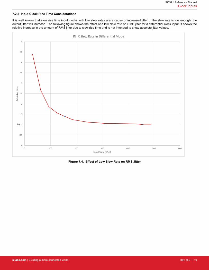
7.2.5 Input Clock Rise Time Considerations
It is well known that slow rise time input clocks with low slew rates are a cause of increased jitter. If the slew rate is low enough, theoutput jitter will increase. The following figure shows the effect of a low slew rate on RMS jitter for a differential clock input. It shows therelative increase in the amount of RMS jitter due to slow rise time and is not intended to show absolute jitter values.
0
0.5
1
1.5
2
2.5
3
3.5
4
4.5
5
0 100 200 300 400 500 600
Rela
teiv
e Jit
ter
Input Slew (V/us)
IN_X Slew Rate in Differential Mode
JTYP
Figure 7.4. Effect of Low Slew Rate on RMS Jitter
Si5391 Reference ManualClock Inputs
silabs.com | Building a more connected world. Rev. 0.2 | 19
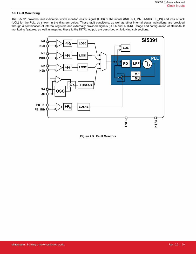
7.3 Fault Monitoring
The Si5391 provides fault indicators which monitor loss of signal (LOS) of the inputs (IN0, IN1, IN2, XA/XB, FB_IN) and loss of lock(LOL) for the PLL, as shown in the diagram below. These fault conditions, as well as other internal status indications, are providedthrough a combination of internal registers and externally provided signals (LOLb and INTRb). Usage and configuration of status/faultmonitoring features, as well as mapping these to the INTRb output, are described on following sub sections.
PLLLPFPD
Mn
IN0IN0b
LOS0÷P0
IN1IN1b
÷P1
FB_INFB _INb
IN2IN2b
÷P2
LOL
Si5391
XBXA OSC
÷Pfb
Md÷
LOSXAB
LOS1
LOS2
LOLb
INTR
b
LOSFB
Figure 7.5. Fault Monitors
Si5391 Reference ManualClock Inputs
silabs.com | Building a more connected world. Rev. 0.2 | 20

7.3.1 Status Indicators
The state of the status monitors are accessible by reading registers through the serial interface or with dedicated pin (LOLb). Each ofthe status indicator register bits has a corresponding sticky bit (_FLG) in a separate register location. Once a status bit is asserted itscorresponding _FLG bit will remain asserted until cleared. Writing a logic zero to a _FLG register bit clears its state.
Table 7.3. Status Monitor Bits
Setting Name Hex Address [Bit Field] Function
Status Register Bits
SYSINCAL 0x000C[0] Asserted when in calibration.
LOSXAXB 0x000C[1]Loss of Signal at the XA input.
The Xb input does not have an LOS detector.
LOSREF 0x000C[2] Loss of Signal for the input that has been selected.
LOL 0x000C[3] Loss of Lock for the PLL.
SMBUS_TIMEOUT 0x000C[5] The SMB bus has a timeout.
LOSIN[3:0] 0x000D[3:0] Loss of Signal for the FB_IN, IN2, IN1, IN0 inputs.
Sticky Status Register Bits
SYSINCAL_FLG 0x0011[0] Sticky bit for SYSINCAL
LOSXAXB_FLG 0x0011[1] Sticky bit for LOSXAXBB
LOSREF_FLG 0x0011[2] Sticky bit for LOSREF
LOL_FLG 0x0011[3] Sticky bit for LOL
SMBUS_TIMEOUT_FLG 0x0011[5] Sticky bit for SMBUS_TIMEOUT
LOSIN_FLG 0x0012[3:0] Sticky bit for FB_IN, IN2, IN1, IN0
Si5391 Reference ManualClock Inputs
silabs.com | Building a more connected world. Rev. 0.2 | 21
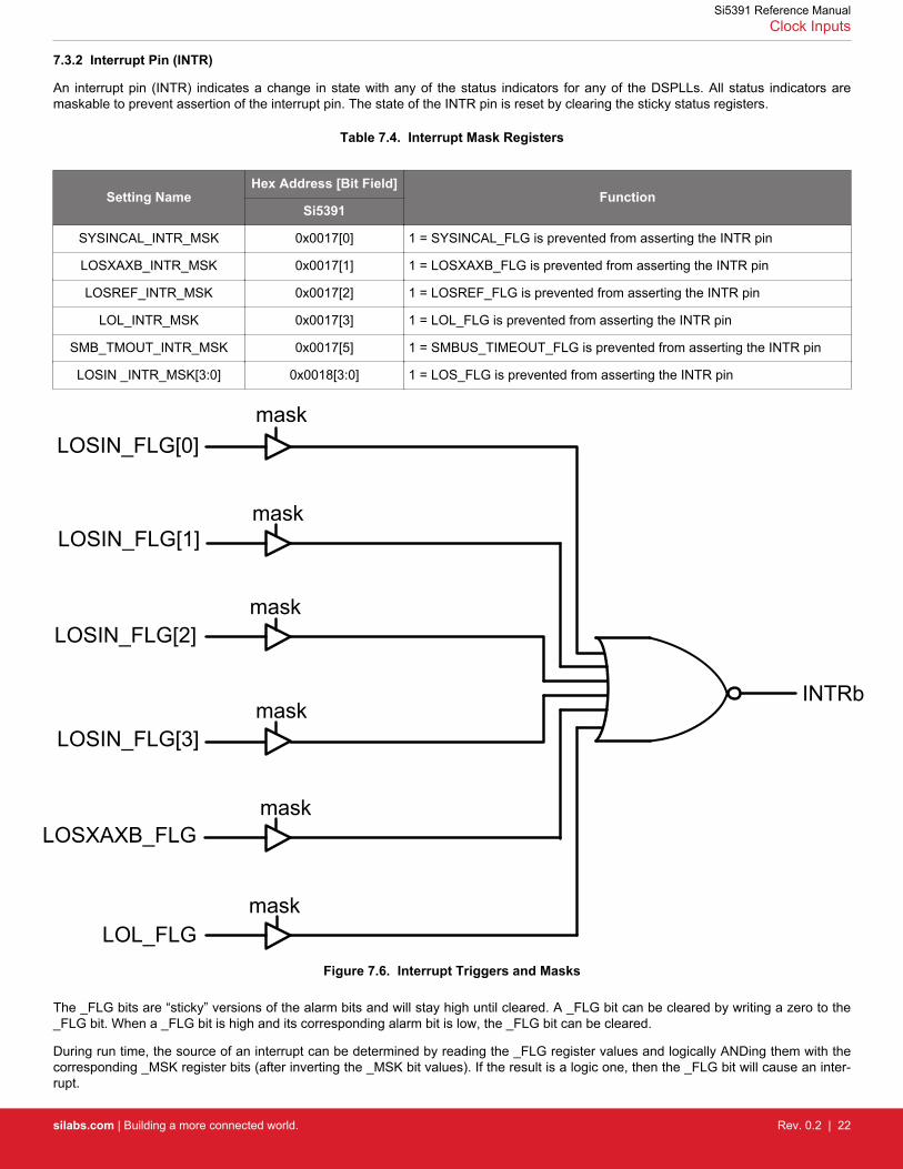
7.3.2 Interrupt Pin (INTR)
An interrupt pin (INTR) indicates a change in state with any of the status indicators for any of the DSPLLs. All status indicators aremaskable to prevent assertion of the interrupt pin. The state of the INTR pin is reset by clearing the sticky status registers.
Table 7.4. Interrupt Mask Registers
Setting NameHex Address [Bit Field]
FunctionSi5391
SYSINCAL_INTR_MSK 0x0017[0] 1 = SYSINCAL_FLG is prevented from asserting the INTR pin
LOSXAXB_INTR_MSK 0x0017[1] 1 = LOSXAXB_FLG is prevented from asserting the INTR pin
LOSREF_INTR_MSK 0x0017[2] 1 = LOSREF_FLG is prevented from asserting the INTR pin
LOL_INTR_MSK 0x0017[3] 1 = LOL_FLG is prevented from asserting the INTR pin
SMB_TMOUT_INTR_MSK 0x0017[5] 1 = SMBUS_TIMEOUT_FLG is prevented from asserting the INTR pin
LOSIN _INTR_MSK[3:0] 0x0018[3:0] 1 = LOS_FLG is prevented from asserting the INTR pin
mask
mask
mask
mask
mask
maskLOL_FLG
LOSXAXB_FLG
LOSIN_FLG[3]
LOSIN_FLG[2]
LOSIN_FLG[1]
LOSIN_FLG[0]
INTRb
Figure 7.6. Interrupt Triggers and Masks
The _FLG bits are “sticky” versions of the alarm bits and will stay high until cleared. A _FLG bit can be cleared by writing a zero to the_FLG bit. When a _FLG bit is high and its corresponding alarm bit is low, the _FLG bit can be cleared.
During run time, the source of an interrupt can be determined by reading the _FLG register values and logically ANDing them with thecorresponding _MSK register bits (after inverting the _MSK bit values). If the result is a logic one, then the _FLG bit will cause an inter-rupt.
Si5391 Reference ManualClock Inputs
silabs.com | Building a more connected world. Rev. 0.2 | 22

For example, if LOS_FLG[0] is high and LOS_INTR_MSK[0] is low, then the INTR pin will be active (low) and cause an interrupt. IfLOS[0] is zero and LOS_MSK[0] is one, writing a zero to LOS_MSK[0] will clear the interrupt (assuming that there are no other interruptsources). If LOS[0] is high, then LOS_FLG[0] and the interrupt cannot be cleared.
Si5391 Reference ManualClock Inputs
silabs.com | Building a more connected world. Rev. 0.2 | 23
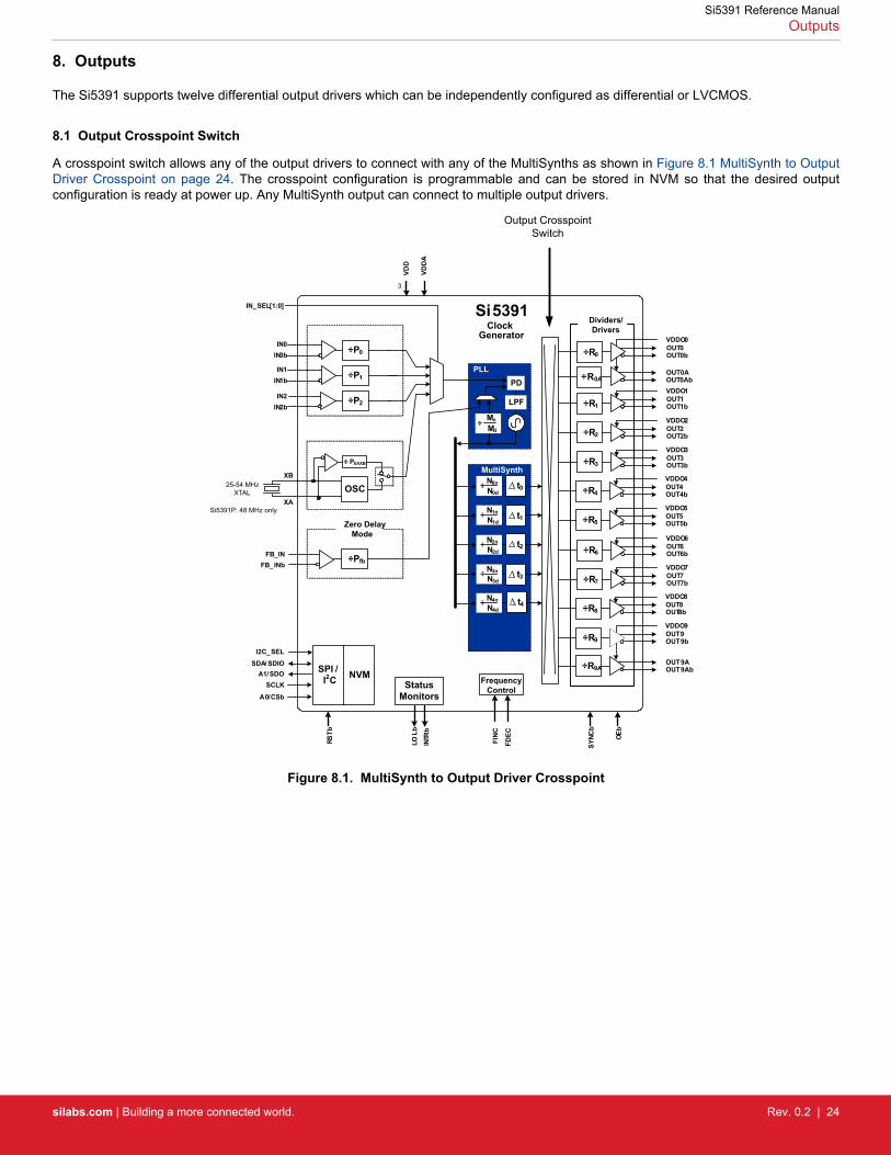
8. Outputs
The Si5391 supports twelve differential output drivers which can be independently configured as differential or LVCMOS.
8.1 Output Crosspoint Switch
A crosspoint switch allows any of the output drivers to connect with any of the MultiSynths as shown in Figure 8.1 MultiSynth to OutputDriver Crosspoint on page 24. The crosspoint configuration is programmable and can be stored in NVM so that the desired outputconfiguration is ready at power up. Any MultiSynth output can connect to multiple output drivers.
VDD
VDD
A
3
SDA/ SDIOA1/SDO
SCLK
A0/CSb
I2C_SEL
SPI /I2C NVM
RSTb
Zero Delay Mode
FB_INFB_INb
OEb
Si5391Generator
Clock
÷R0
÷R2
÷R3
÷R4
÷R5
÷R6
÷R7
÷R8
÷R9
÷R1
OUT0b
VDDO0OUT0
OUT2b
VDDO2OUT2
OUT3b
VDDO3OUT3
OUT4b
VDDO4OUT4
OUT5b
VDDO5OUT5
OUT6b
VDDO6OUT6
OUT7b
VDDO7OUT7
OUT8b
VDDO8OUT8
OUT9b
VDDO9OUT9
OUT1b
VDDO1OUT1
÷Pfb
LPF
PD
÷Mn
Md
PLL
IN_SEL[1:0]
XA
XB
÷P2
÷P1
÷P0IN0
IN0b
IN1IN1b
IN2IN2b
FDEC
FIN
C
Frequency Control
÷ N0nN0d
t0
÷ N2nN2d
÷ N3nN3d
÷ N4nN4d
t2
t3
t4
÷ N1nN1d
t1
MultiSynth
SYNC
b
Dividers/Drivers
StatusMonitors
LOLb
INTR
b
OSC
÷ PXAXB
25-54 MHzXTAL
÷R9A OUT9AbOUT9A
÷R0A OUT0AbOUT0A
Si5391P: 48 MHz only
Output Crosspoint Switch
Figure 8.1. MultiSynth to Output Driver Crosspoint
Si5391 Reference ManualOutputs
silabs.com | Building a more connected world. Rev. 0.2 | 24

Table 8.1. Output Driver Crosspoint Configuration Registers
Setting Name Hex Address[Bit Field]
Function
Si5391/Si5391P
OUT0A_MUX_SEL 0106[2:0] Connects the output drivers to one of the N dividers. Selections are N0, N1,N2, N3, and N4 for each output divider.
OUT0_MUX_SEL 010B[2:0]
OUT1_MUX_SEL 0110[2:0]
OUT2_MUX_SEL 0115[2:0]
OUT3_MUX_SEL 011A[2:0]
OUT4_MUX_SEL 011F[2:0]
OUT5_MUX_SEL 0124[2:0]
OUT6_MUX_SEL 0129[2:0]
OUT7_MUX_SEL 012E[2:0]
OUT8_MUX_SEL 0133[2:0]
OUT9_MUX_SEL 0138[2:0]
OUT9A_MUX_SEL 013D[2:0]
8.2 Output Divider (R) Synchronization
All the output R dividers are reset to the default NVM register state after a power-up or a hard reset. This ensures consistent and re-peatable phase alignment across all output drivers. Resetting the device using the RSTb pin or asserting the hard reset bit will have thesame result. The SYNCb pin provides another method of realigning the R dividers without resetting the device. This pin is positive edgetriggered. Asserting the sync register bit provides the same function. Note that using the SYNCb bit/pin guarantees that the outputs willalign to within 50 ns.
Si5391 Reference ManualOutputs
silabs.com | Building a more connected world. Rev. 0.2 | 25

8.3 Performance Guidelines for Outputs
Whenever a number of high frequency, fast rise time, large amplitude signals are all close to one another there will be some amount ofcrosstalk. The jitter generation of the Si5391/Si5391P is so low that crosstalk can become a significant portion of the final measuredoutput jitter. Some of the crosstalk will come from the Si5391/Si5391P, and some will be introduced by the PCB. It is difficult (and possi-bly irrelevant) to allocate the jitter portions between these two sources since the Si5391/Si5391P must be attached to a board in orderto measure jitter.
For extra fine tuning and optimization in addition to following the usual PCB layout guidelines, crosstalk can be minimized by modifyingthe arrangements of different output clocks. For example, consider the following lineup of output clocks in following table.
Table 8.2. Example of Output Clock Placement
Output Not Recommended(Frequency MHz)
Recommended(Frequency MHz)
0 155.52 155.52
1 156.25 155.52
2 155.52 622.08
3 156.25 Not used
4 200 156.25
5 100 156.25
6 622.08 625
7 625 Not used
8 Not used 200
9 Not used 100
Using this example, a few guidelines are illustrated:1. Avoid adjacent frequency values that are close. For example, a 155.52 MHz clock should not be placed next to a 156.25 MHz
clock. If the jitter integration bandwidth goes up to 20 MHz then keep adjacent frequencies at least 20 MHz apart.2. Adjacent frequency values that are integer multiples of one another are allowed, and these outputs should be grouped together
when possible. Noting that because 155.52 MHz x 4 = 622.08 MHz and 156.25 MHz x 4 = 625 MHz, it is okay to place each pair ofthese frequency values close to one another.
3. Unused outputs can be used to separate clock outputs that might otherwise interfere with one another. In this case, see OUT3 andOUT4.
If some outputs have tight jitter requirements while others are relatively loose, rearrange the clock outputs so that the critical outputs arethe least susceptible to crosstalk. These guidelines need to be followed by those applications that wish to achieve the highest possiblelevels of jitter performance. Because CMOS outputs have large pk-pk swings, are single ended, and do not present a balanced load tothe VDDO supplies, CMOS outputs generate much more crosstalk than differential outputs. For this reason, CMOS outputs should beavoided in jitter-sensitive applications. When CMOS clocks are unavoidable, even greater care must be taken with respect to the aboveguidelines. For more information on these issues, see application note, "AN862: Optimizing Si534x Jitter Performance in Next Genera-tion Internet Infrastructure Systems.”
The ClockBuilder Pro Clock Placement Wizard is an easy way to reduce crosstalk for a given frequency plan. This feature can be ac-cessed on the “Define Output Frequencies” page of ClockBuilder Pro in the lower left hand corner of the GUI. It is recommended to usethis tool after each project frequency plan change.
Si5391 Reference ManualOutputs
silabs.com | Building a more connected world. Rev. 0.2 | 26
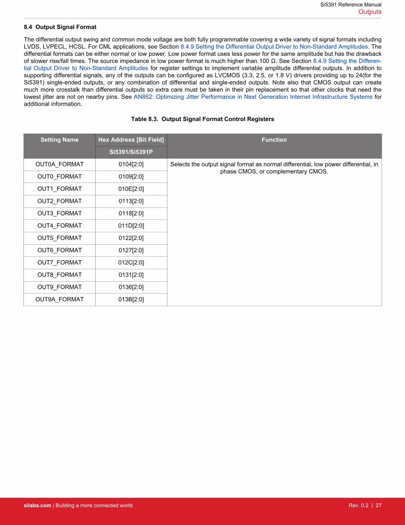
8.4 Output Signal Format
The differential output swing and common mode voltage are both fully programmable covering a wide variety of signal formats includingLVDS, LVPECL, HCSL. For CML applications, see Section 8.4.9 Setting the Differential Output Driver to Non-Standard Amplitudes. Thedifferential formats can be either normal or low power. Low power format uses less power for the same amplitude but has the drawbackof slower rise/fall times. The source impedance in low power format is much higher than 100 Ω. See Section 8.4.9 Setting the Differen-tial Output Driver to Non-Standard Amplitudes for register settings to implement variable amplitude differential outputs. In addition tosupporting differential signals, any of the outputs can be configured as LVCMOS (3.3, 2.5, or 1.8 V) drivers providing up to 24(for theSi5391) single-ended outputs, or any combination of differential and single-ended outputs. Note also that CMOS output can createmuch more crosstalk than differential outputs so extra care must be taken in their pin replacement so that other clocks that need thelowest jitter are not on nearby pins. See AN862: Optimizing Jitter Performance in Next Generation Internet Infrastructure Systems foradditional information.
Table 8.3. Output Signal Format Control Registers
Setting Name Hex Address [Bit Field] Function
Si5391/Si5391P
OUT0A_FORMAT 0104[2:0] Selects the output signal format as normal differential, low power differential, inphase CMOS, or complementary CMOS.
OUT0_FORMAT 0109[2:0]
OUT1_FORMAT 010E[2:0]
OUT2_FORMAT 0113[2:0]
OUT3_FORMAT 0118[2:0]
OUT4_FORMAT 011D[2:0]
OUT5_FORMAT 0122[2:0]
OUT6_FORMAT 0127[2:0]
OUT7_FORMAT 012C[2:0]
OUT8_FORMAT 0131[2:0]
OUT9_FORMAT 0136[2:0]
OUT9A_FORMAT 013B[2:0]
Si5391 Reference ManualOutputs
silabs.com | Building a more connected world. Rev. 0.2 | 27

8.4.1 Differential Output Terminations
The differential output drivers support both ac and dc-coupled terminations as shown in the following figure.
100
50
50
Internally self-biased
AC Coupled LVDS/LVPECL
50
50
AC Coupled LVPECL/CML
VDD – 1.3 V
5050
50
50
100
DC Coupled LVDS
OUTx
OUTx
OUTx
OUTxb
VDDO = 3.3 V, 2.5 V, 1.8 V
VDDO = 3.3 V, 2.5 V
VDDO = 3.3 V, 2.5 V
VDDO = 3.3 V, 2.5 V, 1.8 V
AC Coupled HCSL
R1
OUTx
50
50
R1
R2 R2
VDDRX
Standard HCSLReceiver
OUTxbOUTxb
OUTxb
Clock IC
Clock ICClock IC
Clock IC
VDD RX R1 R23.3 V
1.8 V2.5 V
442332
243
56.259
63.4
For VCM = 0.37 V
ΩΩΩ Ω
ΩΩ
Figure 8.2. Supported Differential Output Terminations
Si5391 Reference ManualOutputs
silabs.com | Building a more connected world. Rev. 0.2 | 28

8.4.2 Differential Output Swing Modes
There are two selectable differential output swing modes: Normal and High (also called low power mode). Each output can support aunique mode.
Differential Normal Swing Mode—This is the usual selection for differential outputs and should be used, unless there is a specific rea-son to do otherwise. When an output driver is configured in normal swing mode, its output swing is selectable as one of 7 settingsranging from 200 mVpp_se to 800 mVpp_se in increments of 100 mV. Differential Output Voltage Swing Control Registers lists theregisters that control the output voltage swing. The output impedance in the Normal Swing Mode is 100 Ω differential. Any of the termi-nations shown in Figure 8.2 Supported Differential Output Terminations on page 28 are supported in this mode.
Differential High Swing Mode—When an output driver is configured in high swing mode, its output swing is configurable as one of 7settings ranging from 400 mVpp_se to 1600 mVpp_se in increments of 200 mV. The output driver is in high impedance mode and sup-ports standard 50 Ω PCB traces. Any of the terminations shown in Figure 8.2 Supported Differential Output Terminations on page 28are supported. The use of High Swing mode will result in larger pk-pk output swings that draw less power. The trade off will be slowerrise and fall times.
Vpp_diff is 2 x Vpp_se as shown below.
OUTx
OUTxVpp_se
Vpp_seVpp_diff = 2*Vpp_se
Vcm
Vcm Vcm
Figure 8.3. Vpp_se and Vpp_diff
Table 8.4. Differential Output Voltage Swing Control Registers
Setting Name Hex Address [Bit Field] Function
Si5391/Si5391P
OUT0A_AMPL 0105[6:4] Sets the voltage swing (amplitude) for the differential output drivers when inNormal differential format and Low Power differential format (Table 8.10 Set-
tings for LVDS, LVPECL, and HCSL on page 33).OUT0_AMPL 010A[6:4]
OUT1_AMPL 010F[6:4]
OUT2_AMPL 0114[6:4]
OUT3_AMPL 0119[6:4]
OUT4_AMPL 011E[6:4]
OUT5_AMPL 0123[6:4]
OUT6_AMPL 0128[6:4]
OUT7_AMPL 012D[6:4]
OUT8_AMPL 0132[6:4]
OUT9_AMPL 0137[6:4]
OUT9A_AMPL 013C[6:4]
Si5391 Reference ManualOutputs
silabs.com | Building a more connected world. Rev. 0.2 | 29

8.4.3 Programmable Common Mode Voltage for Differential Outputs
The common mode voltage (VCM) for the differential Normal and High Swing modes is programmable in 100 mV increments from 0.7to 2.3 V depending on the voltage available at the output's VDDO pin. Setting the common mode voltage is useful when dc coupling theoutput drivers. High swing mode may also cause an increase in the rise/fall time.
Table 8.5. Differential Output Common Mode Voltage Control Registers
Setting Name Hex Address [BitField]
Function
Si5391/Si5391P
OUT0A_CM 0105[3:0] Sets the common mode voltage for the differential output driver.See Table 8.10 Settings for LVDS, LVPECL, and HCSL on page
33 for more information.OUT0_CM 010A[3:0]
OUT1_CM 010F[3:0]
OUT2_CM 0114[3:0]
OUT3_CM 0119[3:0]
OUT4_CM 011E[3:0]
OUT5_CM 0123[3:0]
OUT6_CM 0128[3:0]
OUT7_CM 012D[3:0]
OUT8_CM 0132[3:0]
OUT9_CM 0137[3:0]
OUT9A_CM 013C[3:0]
8.4.4 LVCMOS Output Terminations
LVCMOS outputs are dc-coupled as shown in Figure 8.4 LVCMOS Output Terminations on page 30.
3.3V, 2.5V, 1.8V LVCMOSVDDO = 3.3V, 2.5V, 1.8V
50Rs
50Rs
DC Coupled LVCMOS
OUTx
OUTx
Figure 8.4. LVCMOS Output Terminations
8.4.5 LVCMOS Output Impedance and Drive Strength Selection
Each LVCMOS driver has a configurable output impedance to accommodate different trace impedances and drive strengths. A sourcetermination resistor is recommended to help match the selected output impedance to the trace impedance. There are three programma-ble output impedance selections for each VDDO option as shown below. The value for the OUTx_CMOS_DRIVE bits are given.
Si5391 Reference ManualOutputs
silabs.com | Building a more connected world. Rev. 0.2 | 30
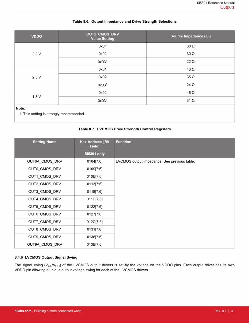
Table 8.6. Output Impedance and Drive Strength Selections
VDDO OUTx_CMOS_DRVValue Setting Source Impedance (ZS)
3.3 V
0x01 38 Ω
0x02 30 Ω
0x031 22 Ω
2.5 V
0x01 43 Ω
0x02 35 Ω
0x031 24 Ω
1.8 V0x02 46 Ω
0x031 31 Ω
Note:1. This setting is strongly recommended.
Table 8.7. LVCMOS Drive Strength Control Registers
Setting Name Hex Address [BitField]
Function
Si5391 only
OUT0A_CMOS_DRV 0104[7:6] LVCMOS output impedance. See previous table.
OUT0_CMOS_DRV 0109[7:6]
OUT1_CMOS_DRV 010E[7:6]
OUT2_CMOS_DRV 0113[7:6]
OUT3_CMOS_DRV 0118[7:6]
OUT4_CMOS_DRV 011D[7:6]
OUT5_CMOS_DRV 0122[7:6]
OUT6_CMOS_DRV 0127[7:6]
OUT7_CMOS_DRV 012C[7:6]
OUT8_CMOS_DRV 0131[7:6]
OUT9_CMOS_DRV 0136[7:6]
OUT9A_CMOS_DRV 013B[7:6]
8.4.6 LVCMOS Output Signal Swing
The signal swing (VOL/VOH) of the LVCMOS output drivers is set by the voltage on the VDDO pins. Each output driver has its ownVDDO pin allowing a unique output voltage swing for each of the LVCMOS drivers.
Si5391 Reference ManualOutputs
silabs.com | Building a more connected world. Rev. 0.2 | 31

8.4.7 LVCMOS Output Polarity
When a driver is configured as an LVCMOS output it generates a clock signal on both pins (OUTx and OUTxb). By default the clock onthe OUTx pin is generated with the same polarity (in phase) with the clock on the OUTxb pin. The polarity of these clocks is configura-ble enabling complimentary clock generation and/or inverted polarity with respect to other output drivers.
Table 8.8. LVCMOS Output Polarity Control Registers
Setting Name Hex Address [Bit Field] Function
Si5391 only
OUT0A_INV 0106[7:6] Controls output polarity of the OUTx and OUTxb pins when in LVCMOS mode.Selections are as below in the Output Polarity Registers.
OUT0_INV 010B[7:6]
OUT1_INV 0110[7:6]
OUT2_INV 0115[7:6]
OUT3_INV 011A[7:6]
OUT4_INV 011F[7:6]
OUT5_INV 0124[7:6]
OUT6_INV 0129[7:6]
OUT7_INV 012E[7:6]
OUT8_INV 0133[7:6]
OUT9_INV 0138[7:6]
OUT9A_INV 013D[7:6]
Table 8.9. Output Polarity of OUTx and OUTxb Pins in LVCMOS Mode
OUTx_INVRegister Settings OUTx OUTxb Comment
00 CLK CLK Both in phase (default)
01 CLK CLKb OUTxb inverted
10 CLKb CLKb OUTx and OUTxb inverted
11 CLKb CLK OUTx inverted
Si5391 Reference ManualOutputs
silabs.com | Building a more connected world. Rev. 0.2 | 32
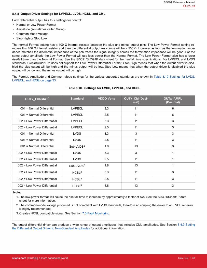
8.4.8 Output Driver Settings for LVPECL, LVDS, HCSL, and CML
Each differential output has four settings for control:• Normal or Low Power Format• Amplitude (sometimes called Swing)• Common Mode Voltage• Stop High or Stop Low
The normal Format setting has a 100 Ω internal resistor between the plus and minus output pins. The Low Power Format setting re-moves this 100 Ω internal resistor and then the differential output resistance will be > 500 Ω. However as long as the termination impe-dance matches the differential impedance of the pcb traces the signal integrity across the termination impedance will be good. For thesame output amplitude the Low Power Format will use less power than the Normal Format. The Low Power Format also has a lowerrise/fall time than the Normal Format. See the Si5391/Si5391P data sheet for the rise/fall time specifications. For LVPECL and LVDSstandards, ClockBuilder Pro does not support the Low Power Differential Format. Stop High means that when the output driver is disa-bled the plus output will be high and the minus output will be low. Stop Low means that when the output driver is disabled the plusoutput will be low and the minus output will be high.
The Format, Amplitude and Common Mode settings for the various supported standards are shown in Table 8.10 Settings for LVDS,LVPECL, and HCSL on page 33.
Table 8.10. Settings for LVDS, LVPECL, and HCSL
OUTx_FORMAT1 Standard VDDO Volts OUTx_CM (Deci-mal)
OUTx_AMPL(Decimal)
001 = Normal Differential LVPECL 3.3 11 6
001 = Normal Differential LVPECL 2.5 11 6
002 = Low Power Differential LVPECL 3.3 11 3
002 = Low Power Differential LVPECL 2.5 11 3
001 = Normal Differential LVDS 3.3 3 3
001 = Normal Differential LVDS 2.5 11 3
001 = Normal Differential Sub-LVDS2 1.8 13 3
002 = Low Power Differential LVDS 3.3 3 1
002 = Low Power Differential LVDS 2.5 11 1
002 = Low Power Differential Sub-LVDS2 1.8 13 1
002 = Low Power Differential HCSL3 3.3 11 3
002 = Low Power Differential HCSL3 2.5 11 3
002 = Low Power Differential HCSL3 1.8 13 3
Note:1. The low-power format will cause the rise/fall time to increase by approximately a factor of two. See the Si5391/Si5391P data
sheet for more information.2. The common-mode voltage produced is not compliant with LVDS standards; therefore ac coupling the driver to an LVDS receiver
is highly recommended.3. Creates HCSL compatible signal. See Section 7.3 Fault Monitoring.
The output differential driver can produce a wide range of output amplitudes that includes CML amplitudes. See Section 8.4.9 Settingthe Differential Output Driver to Non-Standard Amplitudes for additional information.
Si5391 Reference ManualOutputs
silabs.com | Building a more connected world. Rev. 0.2 | 33
8.4.9 Setting the Differential Output Driver to Non-Standard Amplitudes
In some applications, it may be desirable to have larger or smaller differential amplitudes than those produced by the standard LVPECLand LVDS settings, as selected by CBPro. In these cases, the following information describes how to implement these amplitudes bywriting to the OUTx_CM and OUTx_AMPL setting names. Contact Silicon Labs for assistance if you want your custom configured de-vice to be programmed for any of the settings described here.
The differential output driver has a variable output amplitude capability and two basic formats, normal and low-power format. The differ-ence between these two formats is that the normal format has an output impedance of ~100 Ω differential, and the low-power formathas an output impedance of > 500 Ω differential. Note that the rise/fall time is slower when using the Low Power Differential Format.See the Si5391/Si5391P data sheet for rise/fall time specifications.
If the standard LVDS or LVPECL compatible output amplitudes will not work for a particular application, the variable amplitude capabili-ty can be used to achieve higher or lower amplitudes. For example, a “CML” format is sometimes desired for an application. However,CML is not a defined standard, and hence the amplitude of a CML signal for one receiver may be different than that of another receiver.
When the output amplitude needs to be different than standard LVDS or LVPECL, the Common Mode Voltage settings must be set asshown in Table 8.11 Output Differential Common Mode Voltage Settings on page 34. No settings other than these are supported asthe signal integrity could be compromised. In addition, the output driver should be ac-coupled to the load so that the common-modevoltage of the driver is not affected by the load.
Table 8.11. Output Differential Common Mode Voltage Settings
VDDOx (Volts) Differential Format
OUTx_FORMAT Common Mode Voltage (Volts)
OUTx_CM
3.3 Normal 0x1 2.0 0xB
3.3 Low Power 0x2 1.6 0x7
2.5 Normal 0x1 1.3 0xC
2.5 Low Power 0x2 1.1 0xA
1.8 Normal 0x1 0.8 0xD
1.8 Low Power 0x2 0.8 0xD
The differential amplitude can be set as shown in the following table.
Table 8.12. Typical Differential Amplitudes1
OUTx_AMPL Normal Differential Format
(Vpp SE mV – Typical)
Low-Power Differential Format
(Vpp SE mV – Typical)
0 130 200
1 230 400
2 350 620
3 450 820
4 575 1010
5 700 1200
6 810 13502
7 920 16002
Note:1. These amplitudes are based upon a 100 Ω differential termination.2. In low-power mode and VDDOx = 1.8 V, OUTx_AMPL may not be set to 6 or 7.
Si5391 Reference ManualOutputs
silabs.com | Building a more connected world. Rev. 0.2 | 34

See the register map portion of this document for additional information about OUTx_FORMAT, OUTx_CM and OUTx_AMPL. ContactSilicon Labs for assistance if you require a factory-programmed device to be configured for any of the output driver settings listedabove.
8.5 Output Enable/Disable
Clock outputs are disabled by four signals within Si5391 and the OEB pin:• OUTALL_DISABLE_LOW• SYSINCAL• OUTx_OE• LOL• OEB pin
The following figure shows the logic of how these disable/enables occur.
Enable to IndividualOutput Drivers
LOL
SYSINCAL
OUTALL_DISABLE_LOW
OUTX_OE
OEB Pin
OUTX_OE are the individual Output Driver enables as shown in the table below
1 instance of this is used per output driver
Figure 8.5. Output Enable
Table 8.13. Output Enable/Disable Control Registers
Setting Name Hex Address[Bit Field]
Function
Si5391/Si5391P
OUTALL_DISABLE_LOW 0102[0] 0 = Disables all outputs.
1 = All outputs are not disabled by this signal but may be disabled by othersignals or the OEB pin. See figure above.
OUT0A_OE 0103[1] 0 = Specific output disabled.
1 = Specific output is not disabled. The OEB pin or other signals within thedevice may be causing an output disable. See figure above.
OUT0_OE 0108[1]
OUT1_OE 010D[1]
OUT2_OE 0112[1]
OUT3_OE 0117[1]
OUT4_OE 011C[1]
OUT5_OE 0121[1]
OUT6_OE 0126[1]
OUT7_OE 012B[1]
OUT8_OE 0130[1]
OUT9_OE 0135[1]
OUT9A_OE 013A[1]
Si5391 Reference ManualOutputs
silabs.com | Building a more connected world. Rev. 0.2 | 35

8.5.1 Output Driver State When Disabled
The disabled state of an output driver is configurable as disable low or disable high. When the output driver is disabled, the outputs willdrive either logic high or logic low, selectable by the user. The output common mode voltage is maintained while the driver is disabled,reducing enable/disable transients. By contrast, powering down the driver rather than disabling it increases output impedance and shutsoff the output common mode voltage. For all output drivers connected in the system, it is recommended to use Disable rather thanPowerdown to reduce enable/disable common mode transients. Unused outputs may be left unconnected, powered down to reducecurrent draw, and, with the corresponding VDDOx, left unconnected.
Table 8.14. Output Driver State Control Registers
Setting Name Hex Address[Bit Field]
Function
Si5391/Si5391P
OUT0A_DIS_STATE 0104[5:4] Determines the state of an output driver when disabled. Selectable as:• Disable logical low• Disable logical high
OUT0_DIS_STATE 0109[5:4]
OUT1_DIS_STATE 010E[5:4]
OUT2_DIS_STATE 0113[5:4]
OUT3_DIS_STATE 0118[5:4]
OUT4_DIS_STATE 011D[5:4]
OUT5_DIS_STATE 0122[5:4]
OUT6_DIS_STATE 0127[5:4]
OUT7_DIS_STATE 012C[5:4]
OUT8_DIS_STATE 0131[5:4]
OUT9_DIS_STATE 0136[5:4]
OUT9A_DIS_STATE 013B[5:4]
Si5391 Reference ManualOutputs
silabs.com | Building a more connected world. Rev. 0.2 | 36
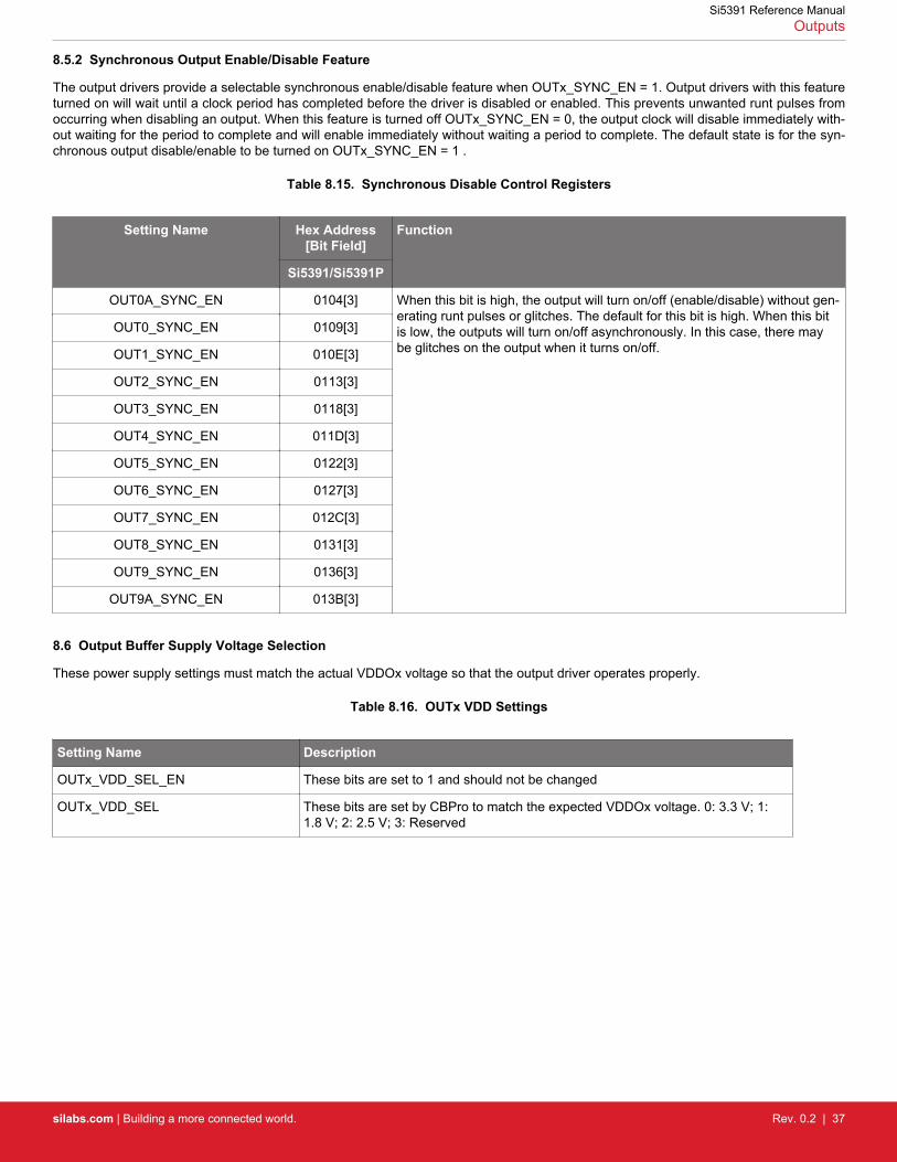
8.5.2 Synchronous Output Enable/Disable Feature
The output drivers provide a selectable synchronous enable/disable feature when OUTx_SYNC_EN = 1. Output drivers with this featureturned on will wait until a clock period has completed before the driver is disabled or enabled. This prevents unwanted runt pulses fromoccurring when disabling an output. When this feature is turned off OUTx_SYNC_EN = 0, the output clock will disable immediately with-out waiting for the period to complete and will enable immediately without waiting a period to complete. The default state is for the syn-chronous output disable/enable to be turned on OUTx_SYNC_EN = 1 .
Table 8.15. Synchronous Disable Control Registers
Setting Name Hex Address[Bit Field]
Function
Si5391/Si5391P
OUT0A_SYNC_EN 0104[3] When this bit is high, the output will turn on/off (enable/disable) without gen-erating runt pulses or glitches. The default for this bit is high. When this bitis low, the outputs will turn on/off asynchronously. In this case, there maybe glitches on the output when it turns on/off.
OUT0_SYNC_EN 0109[3]
OUT1_SYNC_EN 010E[3]
OUT2_SYNC_EN 0113[3]
OUT3_SYNC_EN 0118[3]
OUT4_SYNC_EN 011D[3]
OUT5_SYNC_EN 0122[3]
OUT6_SYNC_EN 0127[3]
OUT7_SYNC_EN 012C[3]
OUT8_SYNC_EN 0131[3]
OUT9_SYNC_EN 0136[3]
OUT9A_SYNC_EN 013B[3]
8.6 Output Buffer Supply Voltage Selection
These power supply settings must match the actual VDDOx voltage so that the output driver operates properly.
Table 8.16. OUTx VDD Settings
Setting Name Description
OUTx_VDD_SEL_EN These bits are set to 1 and should not be changed
OUTx_VDD_SEL These bits are set by CBPro to match the expected VDDOx voltage. 0: 3.3 V; 1:1.8 V; 2: 2.5 V; 3: Reserved
Si5391 Reference ManualOutputs
silabs.com | Building a more connected world. Rev. 0.2 | 37
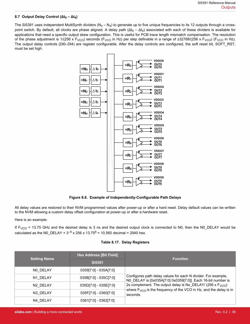
8.7 Output Delay Control (Δt0 – Δt4)
The Si5391 uses independent MultiSynth dividers (N0 – N4) to generate up to five unique frequencies to its 12 outputs through a cross-point switch. By default, all clocks are phase aligned. A delay path (Δt0 – Δt4) associated with each of these dividers is available forapplications that need a specific output skew configuration. This is useful for PCB trace length mismatch compensation. The resolutionof the phase adjustment is 1/(256 x FVCO) seconds (FVCO in Hz) per step definable in a range of ±32768/(256 x FVCO) (FVCO in Hz).The output delay controls (Dt0–Dt4) are register configurable. After the delay controls are configured, the soft reset bit, SOFT_RST,must be set high.
÷N0 t0
÷N1 t1
÷N2 t2
÷N3 t3
÷N4 t4
OUT2
VDDO2OUT2
VDDO3
÷R2
OUT3OUT3÷R3
OUT1
VDDO1OUT1÷R1
OUT5
VDDO5OUT5
VDDO6
÷R5
OUT6OUT6÷R6
OUT4
VDDO4OUT4÷R4
OUT7
VDDO7OUT7
VDDO8
÷R7
OUT8OUT8÷R8
OUT0
VDDO0OUT0÷R0
VDDO9
OUT9OUT9÷R9
Figure 8.6. Example of Independently-Configurable Path Delays
All delay values are restored to their NVM programmed values after power-up or after a hard reset. Delay default values can be writtento the NVM allowing a custom delay offset configuration at power-up or after a hardware reset.
Here is an example:
If FVCO = 13.75 GHz and the desired delay is 3 ns and the desired output clock is connected to N0, then the N0_DELAY would becalculated as the N0_DELAY = 3–9 x 256 x 13.759 = 10,560 decimal = 2940 hex.
Table 8.17. Delay Registers
Setting NameHex Address [Bit Field]
FunctionSi5391
N0_DELAY 0359[7:0] - 035A[7:0]Configures path delay values for each N divider. For example,N0_DELAY is [0x035A[7:0] 0x0359[7:0]]. Each 16-bit number is2s complement. The output delay is Nx_DELAY/ (256 x FVCO)where FVCO is the frequency of the VCO in Hz, and the delay is inseconds.
N1_DELAY 035B[7:0] - 035C[7:0]
N2_DELAY 035D[7:0] - 035E[7:0]
N3_DELAY 035F[7:0] - 0360[7:0]
N4_DELAY 0361[7:0] - 0362[7:0]
Si5391 Reference ManualOutputs
silabs.com | Building a more connected world. Rev. 0.2 | 38

9. Zero Delay Mode (All Si5391 Devices Except Si5391P)
A zero delay mode is available, in all Si5391 devices except for Si5391P, for applications that require fixed and consistent minimumdelay between the selected input and outputs. The zero delay mode is configured by opening the internal feedback loop through soft-ware configuration and closing the loop externally as shown in Figure 9.1 Si5391 Zero Delay Mode Setup on page 39. This helps tocancel out the internal delay introduced by the dividers, the crosspoint, the input, and the output drivers. Any one of the outputs can befed back to the FB_IN pins, although using the output driver that achieves the shortest trace length will help to minimize the input-to-output delay. The OUT11 and FB_IN pins are recommended for the external feedback connection in the Si5391. The FB_IN input pinsmust be terminated and ac-coupled when zero delay mode is used. A differential external feedback path connection is necessary forbest performance. For this reason, customers should avoid using CMOS outputs for driving the external feedback path. Zero DelayMode performance will degrade with low values of phase detector frequency (Fpfd). For this reason, ClockBuilder Pro will not enableZero Delay Mode with an Fpfd of less than 128 kHz.
Zero Delay Mode
IN_SEL[1:0]
IN0IN0b
IN1IN1b
IN2IN2b
÷P0
÷ P1
÷ P2
VDDO0
OUT1b
VDDO1OUT1
OUT2b
VDDO2OUT2
OUT9b
VDDO8OUT8
OUT 9b
VDDO 9OUT9
OUT 9AbOUT9A
MultiSynth& Dividers
IN3/FB_IN
IN3b/FB_INb
100
External Feedback Path
PD
LPF
÷ MnMd
÷ N9nN9d
÷R11
fFB = fIN
fIN
÷Pfb
PLL
OUT0AbOUT 0A
OUT0bOUT0
Figure 9.1. Si5391 Zero Delay Mode Setup
The following table lists the registers used for the Zero Delay mode.
Table 9.1. Zero Delay Mode Registers
Register Name Hex Address[Bit Field] Function
ZDM_EN 0x0487[0]0: Disable zero delay mode.
1: Enable zero delay mode.
ZDM_AUTOSW_EN 0x0487[4]0: Automatic switching disabled for zero-delay mode
1: Automatic input switching enabled and input clock selection governed by au-tomatic input switching engine
Si5391 Reference ManualZero Delay Mode (All Si5391 Devices Except Si5391P)
silabs.com | Building a more connected world. Rev. 0.2 | 39

Table 9.2. Input Clock Selection in Zero Delay Mode
ZDM_AUTO_SW_EN ZDM_EN IN_SEL_REGCTRL Input Clock Selection Governed by
0 0 0 IN_SEL[1:0] Pins
0 0 1 IN_SEL Register
0 1 0 IN_SEL[1:0] Pins
1 X X Input clock selection governed by automatic input switchingengine (see )
Si5391 Reference ManualZero Delay Mode (All Si5391 Devices Except Si5391P)
silabs.com | Building a more connected world. Rev. 0.2 | 40
10. Digitally-Controlled Oscillator (DCO) Mode (All Si5391 Devices Except Si5391P)
An output that is controlled as a DCO is useful for simple tasks such as frequency margining, CPU speed control, or just changing theoutput frequency. The output can also be used for more sophisticated tasks such as FIFO management by adjusting the frequency ofthe read or write clock to the FIFO or using the output as a variable Local Oscillator in a radio application.
10.1 Using the N Dividers for DCO Applications
The N dividers can be digitally controlled to so that all outputs connected to the N divider change frequency in real time without anytransition glitches. There are two ways to control the N divider to accomplish this task:• Use the Frequency Increment/Decrement Pins or register bits.• Write directly to the numerator or denominator of the N divider.
The output N divider can be changed from its minimum value of 10 to its maximum value of 4095 in very small fractional increments ora single very large increment. Each N divider has a value of Nx_NUM/Nx_DEN. Nx_NUM is a 44 bit word and Nx_DEN is a 32 bit word.Clockbuilder Pro left shifts these values as far as possible before writing them to the actual Nx_NUM and Nx_DEN registers. For exam-ple, an integer Nx divider of 30/1, when left shifted, becomes Nx_NUM = 6442509440 (decimal) and Nx_DEN = 2147483648 (decimal).By adjusting the size of the Nx_NUM and Nx_DEN but keeping the ratio the same, the resolution of the LSbit of numerator or denomi-nator can be controlled.
When changing the N divider(s) to fractional values, the setting name N_PIBYP[4:0] must be a 0 for the N divider that is being changed.This applies when using FINC/FDEC or when directly writing to the N divider.
10.1.1 DCO with Frequency Increment/Decrement Pins/Bits
The FSTEPW (Frequency STEP Word) is a 44 bit word that is used to change the value of the Nx_NUM word. Whenever an FINC orFDEC is asserted, the FSTEPW will automatically add or subtract from the Nx_NUM word so that the output frequency will increment(FINC) or decrement (FDEC) respectively.
Each of the N dividers can be independently stepped up or down in numerical predefined steps with a maximum resolution that variesfrom ~ 0.05 ppb to a ~0.004 ppb depending upon the frequency plan. One or more N dividers can be controlled by FINC/FDEC at thesame time by use of the N_FSTEP_MSK bits. Any N divider that is masked by its corresponding bit in the N_FSTEP_MSK field will notchange when FINC or FDEC is asserted. The magnitude of the frequency change caused by FINC or FDEC is determined by the valueof the FSTEPW word and the magnitude of the word in Nx_NUM. For a specific frequency step size it may be necessary to adjust theNx_NUM value while keeping the ratio of Nx_NUM/Nx_DEN the same. When the FINC or FDEC pin or register bit is asserted the se-lected N dividers will have their numerator changed by the addition or subtraction of the Nx_FSTEPW so that an FINC will increase theoutput frequency and an FDEC will decrease the output frequency. An FINC or FDEC can be followed by another FINC or FDEC in 1µs minimum.
Because the output frequency = FVCO * Nx_DEN/(Rx * Nx_NUM), subsequent changes to Nx_NUM by the FSTEPW will not produceexactly the same output frequency change. The amount of error in the frequency step is extremely small and in a vast number of appli-cations will not cause a problem. When consecutive frequency steps must be exactly the same, it is possible to set FINC and FDEC tochange the Nx_DEN instead of Nx_NUM and then consecutive FINCs or FDECs will be exactly the same frequency change. However,there are some special setups that are necessary to achieve this. For more information contact Silicon Labs.
10.1.2 DCO with Direct Register Writes
When a N divider numerator (Nx_NUM) and its corresponding update bit (Nx_UPDATE) is written, the new numerator value will takeeffect and the output frequency will change without any glitches. The N divider numerator and denominator terms (Nx_NUM andNx_DEN) can be left and right shifted so that the least significant bit of the numerator word represents the exact step resolution that isneeded for your application. Each N divider has an update bit (Nx_UPDATE) that must be written to cause the written values to takeeffect. All N dividers can be updated at the same time by writing the N_UPDATE_ALL bit. Note that writing this bit will not cause anyoutput glitching on an N divider that did not have its numerator or denominator changed.
When changing the N divider denominator (Nx_DEN) it is remotely possible that a small phase change of ~550 fs may occur at theexact time of the frequency change. However with the proper setup it is possible to change Nx_DEN and never have a phase change. Ifyour application requires changing an N divider denominator, contact Silicon Labs.
10.2 Using the M Divider for DCO Applications
The VCO can be treated as a DCO by changing the value of the M feedback divider. By changing the M divider, all the output frequen-cies will change by the same amount in ppm. Changing the M divider is only valid for small changes in the output frequencies. ContactSilicon Labs for assistance in the implementation of this capability.
Si5391 Reference ManualDigitally-Controlled Oscillator (DCO) Mode (All Si5391 Devices Except Si5391P)
silabs.com | Building a more connected world. Rev. 0.2 | 41

11. Serial Interface
Configuration and operation of the Si5391/Si5391P is controlled by reading and writing registers using the I2C or SPI serial interface.The I2C_SEL pin selects between I2C or SPI operation. The Si5391/Si5391P supports communication with either a 3.3 V or 1.8 V hostby setting the IO_VDD_SEL (0x0943[0]) configuration bit. The SPI mode supports 4-wire or 3-wire by setting the SPI_3WIRE configura-tion bit. See the figure below for supported modes of operation and settings. The I2C pins are open drain and are ESD clamped to 3.3V, regardless of the host supply level. The I2C pins are clamped to 3.3 V so that they may be externally pulled up to 3.3 V regardless ofIO_VDD_SEL (in register 0x0943).
The table below lists register settings of interest for the I2C/SPI.
VDDA VDD
1.8V3.3V
Host = 3.3V
Host = 1.8V
I2C
I2C_SEL pin = High
IO_VDD_SEL = 0 IO_VDD_SEL = 0
I2C_SEL pin = Low
SPI HOST
1.8V
SDISDOCSbCSb
SDOSDISCLKSCLK
Clock IC
I2C HOST
1.8V
VDDA
SCLK
SDA
1.8V
VDD
1.8V3.3V
SPI HOST
1.8V
SDIOSDIOCSbCSb
SCLKSCLK
SPI_3WIRE = 0
SPI 4-Wire SPI 3-Wire
I2C_SEL pin = LowSPI_3WIRE = 1
IO_VDD_SEL = 0
IO_VDD_SEL = 1 IO_VDD_SEL = 1 IO_VDD_SEL = 1
SCLK
SDA
(Default) (Default)
VDDA VDD
1.8V3.3V
(Default)
VDDA VDD
1.8V3.3V
SPI HOST
3.3V
SDISDOCSbCSb
SDOSDISCLKSCLK
I2C HOST
3.3V
VDDA
SCLK
SDA
3.3V
VDD
1.8V3.3V
SPI HOST
3.3V
SDIOSDIOCSbCSb
SCLKSCLKSCLK
SDA
VDDA VDD
1.8V3.3V
Clock IC Clock IC
Clock IC Clock IC Clock IC
Figure 11.1. I2C/SPI Device Connectivity Configurations
If neither serial interface is used, leave I2C_SEL unconnected. Pull pins SDA/SDIO, SCLK, A1/SDO, and A0/CS all low.
Note that the Si5391/Si5391P is not I2C fail-safe upon loss of power. Applications that require fail-safe operation should isolate the de-vice from a shared I2C bus.
Si5391 Reference ManualSerial Interface
silabs.com | Building a more connected world. Rev. 0.2 | 42

Table 11.1. I2C/SPI Register Settings
Setting Name Hex Address [Bit Field] Function
Si5391/Si5391P
IO_VDD_SEL 0x0943[0] The IO_VDD_SEL configuration bit optimizes the VIL, VIH, VOL,and VOH thresholds to match the VDDS voltage. By default theIO_VDD_SEL bit is set to the VDD option. The serial interfacepins are always 3.3 V tolerant even when the device's VDD pin issupplied from a 1.8 V source. When the I2C or SPI host is operat-ing at 3.3 V and the Si5391/Si5391P at VDD = 1.8 V, the hostmust write the IO_VDD_SEL configuration bit to the VDDA option.This will ensure that both the host and the serial interface are op-erating at the optimum voltage thresholds.
SPI_3WIRE 0x002B[3] The SPI_3WIRE configuration bit selects the option of 4-wire or 3-wire SPI communication. By default, this configuration bit is set tothe 4-wire option. In this mode the Si5391/Si5391P will acceptwrite commands from a 4-wire or 3- wire SPI host allowing config-uration of device registers. For full bidirectional communication in3-wire mode, the host must write the SPI_3WIRE configuration bitto “1”.
Si5391 Reference ManualSerial Interface
silabs.com | Building a more connected world. Rev. 0.2 | 43

11.1 I2C Interface
When in I2C mode, the serial interface operates in slave mode with 7-bit addressing and can operate in Standard-Mode (100 kbps) orFast-Mode (400 kbps) and supports burst data transfer with auto address increments. The I2C bus consists of a bidirectional serial dataline (SDA) and a serial clock input (SCL) as shown in the figure below. Both the SDA and SCL pins must be connected to a supply viaan external pull-up (4.7 kΩ) as recommended by the I2C specification as shown in the figure below. Two address select bits (A0, A1)are provided allowing up to four Si5391/Si5391P devices to communicate on the same bus. This also allows four choices in the I2Caddress for systems that may have other overlapping addresses for other I2C devices.
SDA
SCLK
Clock IC
I2C_SEL
VDDVDDI2C
To I2C Bus or Host
A0A1
LSBs of I2C Address
I2C
Figure 11.2. I2C Configuration
The 7-bit slave device address of the Si5391/Si5391P consists of a 5-bit fixed address plus 2 pins which are selectable for the last twobits, as shown in the following figure.
Slave Address 1 1 1 0 1 A0
0123456
A1
Figure 11.3. 7-bit I2C Slave Address Bit-Configuration
Data is transferred MSB first in 8-bit words as specified by the I2C specification. A write command consists of a 7-bit device (slave)address + a write bit, an 8-bit register address, and 8 bits of data as shown in Figure 11.6 SPI Interface Connections on page 46. Awrite burst operation is also shown where subsequent data words are written using to an auto-incremented address.
1 – Read0 – WriteA – Acknowledge (SDA LOW)N – Not Acknowledge (SDA HIGH)S – START conditionP – STOP condition
Write Operation – Single Byte
S 0 A Reg Addr [7:0]Slv Addr [6:0] A Data [7:0] PA
Write Operation - Burst (Auto Address Increment)
Reg Addr +1
S 0 A Reg Addr [7:0]Slv Addr [6:0] A Data [7:0] A Data [7:0] PA
Host
Clock ICHost
Clock IC
Figure 11.4. I2C Write Operation
A read operation is performed in two stages. A data write is used to set the register address, then a data read is performed to retrievethe data from the set address. A read burst operation is also supported. This is shown in the following figure.
Si5391 Reference ManualSerial Interface
silabs.com | Building a more connected world. Rev. 0.2 | 44

1 – Read0 – WriteA – Acknowledge (SDA LOW)N – Not Acknowledge (SDA HIGH)S – START conditionP – STOP condition
Read Operation – Single Byte
S 0 A Reg Addr [7:0]Slv Addr [6:0] A P
Read Operation - Burst (Auto Address Increment)
Reg Addr +1
S 1 ASlv Addr [6:0] Data [7:0] PN
S 0 A Reg Addr [7:0]Slv Addr [6:0] A P
S 1 ASlv Addr [6:0] Data [7:0] A PNData [7:0]
Host
Clock ICHost
Clock IC
Figure 11.5. I2C Read Operation
The SMBUS interface requires a timeout. The error flags are found in the registers listed below.
Table 11.2. SMBus Timeout Error Bit Indicators
Register Name Hex Address [BitField]
Function
SMBUS_TIMEOUT 0x000C[5] 1 if there is a SMBus timeout error.
SMBUS_TIME-OUT_FLG
0x0011[5] 1 if there is a SMBus timeout error.
Si5391 Reference ManualSerial Interface
silabs.com | Building a more connected world. Rev. 0.2 | 45
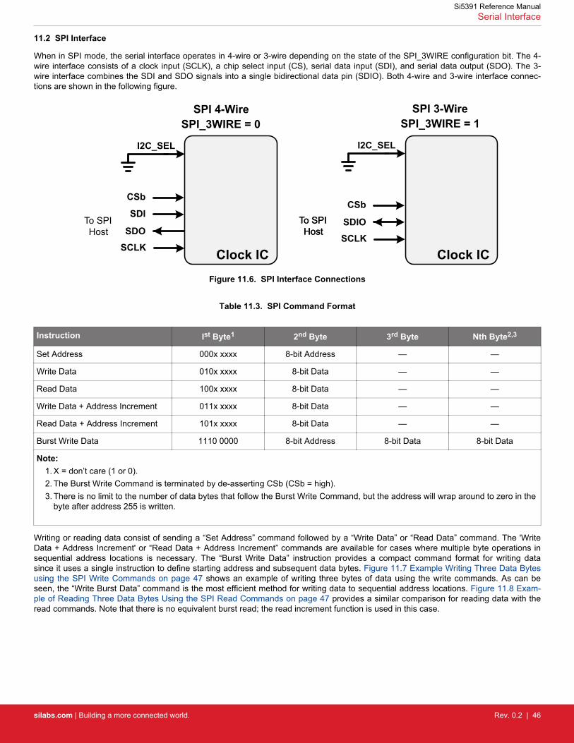
11.2 SPI Interface
When in SPI mode, the serial interface operates in 4-wire or 3-wire depending on the state of the SPI_3WIRE configuration bit. The 4-wire interface consists of a clock input (SCLK), a chip select input (CS), serial data input (SDI), and serial data output (SDO). The 3-wire interface combines the SDI and SDO signals into a single bidirectional data pin (SDIO). Both 4-wire and 3-wire interface connec-tions are shown in the following figure.
To SPI Host
SDI
SDO
Clock IC
I2C_SEL
SCLK
CSb
SPI_3WIRE = 0SPI 4-Wire
CSb
SDIO
I2C_SEL
SCLK
SPI_3WIRE = 1SPI 3-Wire
To SPI Host
To SPI Host
Clock ICFigure 11.6. SPI Interface Connections
Table 11.3. SPI Command Format
Instruction Ist Byte1 2nd Byte 3rd Byte Nth Byte2,3
Set Address 000x xxxx 8-bit Address — —
Write Data 010x xxxx 8-bit Data — —
Read Data 100x xxxx 8-bit Data — —
Write Data + Address Increment 011x xxxx 8-bit Data — —
Read Data + Address Increment 101x xxxx 8-bit Data — —
Burst Write Data 1110 0000 8-bit Address 8-bit Data 8-bit Data
Note:1. X = don’t care (1 or 0).2. The Burst Write Command is terminated by de-asserting CSb (CSb = high).3. There is no limit to the number of data bytes that follow the Burst Write Command, but the address will wrap around to zero in the
byte after address 255 is written.
Writing or reading data consist of sending a “Set Address” command followed by a “Write Data” or “Read Data” command. The 'WriteData + Address Increment' or “Read Data + Address Increment” commands are available for cases where multiple byte operations insequential address locations is necessary. The “Burst Write Data” instruction provides a compact command format for writing datasince it uses a single instruction to define starting address and subsequent data bytes. Figure 11.7 Example Writing Three Data Bytesusing the SPI Write Commands on page 47 shows an example of writing three bytes of data using the write commands. As can beseen, the “Write Burst Data” command is the most efficient method for writing data to sequential address locations. Figure 11.8 Exam-ple of Reading Three Data Bytes Using the SPI Read Commands on page 47 provides a similar comparison for reading data with theread commands. Note that there is no equivalent burst read; the read increment function is used in this case.
Si5391 Reference ManualSerial Interface
silabs.com | Building a more connected world. Rev. 0.2 | 46

‘Set Address’ and ‘Write Data + Address Increment’
‘Burst Write Data’
‘Set Address’ and ‘Write Data’
‘Set Addr’ Addr [7:0] ‘Write Data’ Data [7:0]
‘Set Addr’ Addr [7:0] ‘Write Data’ Data [7:0]
‘Set Addr’ Addr [7:0] ‘Write Data’ Data [7:0]
‘Write Data + Addr Inc’ Data [7:0]
‘Write Data + Addr Inc’ Data [7:0]
‘Set Addr’ Addr [7:0] ‘Write Data + Addr Inc’ Data [7:0]
‘Burst Write Data’ Addr [7:0] Data [7:0] Data [7:0] Data [7:0]
Clock ICHost Clock ICHost
Figure 11.7. Example Writing Three Data Bytes using the SPI Write Commands
‘Set Address’ and ‘Read Data + Address Increment’
‘Set Address’ and ‘Read Data’
‘Set Addr’ Addr [7:0] ‘Read Data’ Data [7:0]
‘Set Addr’ Addr [7:0] ‘Read Data’ Data [7:0]
‘Set Addr’ Addr [7:0] ‘Read Data’ Data [7:0]
‘Read Data + Addr Inc’ Data [7:0]
‘Read Data + Addr Inc’ Data [7:0]
‘Set Addr’ Addr [7:0] ‘Read Data + Addr Inc’ Data [7:0]
Clock ICHost Clock ICHost
Figure 11.8. Example of Reading Three Data Bytes Using the SPI Read Commands
The timing diagrams for the SPI commands are shown in Figures Figure 11.9 SPI “Set Address” Command Timing on page 48, Fig-ure 11.10 SPI “Write Data” and “Write Data+ Address Increment” Instruction Timing on page 49, Figure 11.11 SPI “Read Data” and
Si5391 Reference ManualSerial Interface
silabs.com | Building a more connected world. Rev. 0.2 | 47
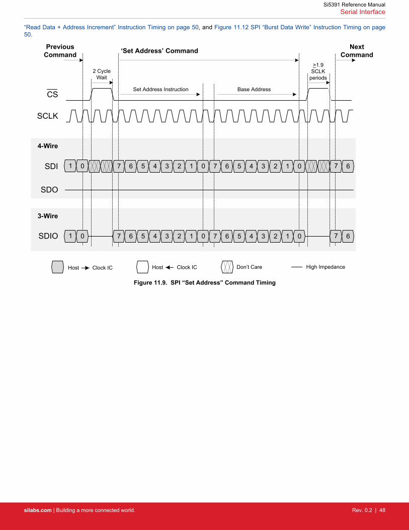
“Read Data + Address Increment” Instruction Timing on page 50, and Figure 11.12 SPI “Burst Data Write” Instruction Timing on page50.
Set Address Instruction Base AddressCS
SCLK
SDI
SDO
SDIO
4-Wire
3-Wire
‘Set Address’ Command
2 Cycle Wait
Previous Command
Next Command
>1.9 SCLK
periods
1 0 01234567 0123456 67
1 0 01234567 0123456 67
Clock ICHost Clock ICHost Don’t Care High Impedance
7
7
Figure 11.9. SPI “Set Address” Command Timing
Si5391 Reference ManualSerial Interface
silabs.com | Building a more connected world. Rev. 0.2 | 48

Write Data instruction
Data byte @ base addressor
Data byte @ base address + 1CS
SCLK
SDI
SDO
SDIO
4-Wire
3-Wire
‘Write Data’
2 Cycle Wait
Previous Command
Next Command
1 0 01234567 01234567 67
1 0 01234567 01234567 67
Clock ICHost Clock ICHost Don’t Care High Impedance
>1.9 SCLK
periods
Figure 11.10. SPI “Write Data” and “Write Data+ Address Increment” Instruction Timing
Si5391 Reference ManualSerial Interface
silabs.com | Building a more connected world. Rev. 0.2 | 49

CS
SCLK
SDI
SDO
SDIO
4-Wire
3-Wire
‘Read Data’
2 Cycle Wait
Previous Command
Next Command
1 0 01234567
1 0 6701234567
1 0 01234567 67
67
01234567
Clock ICHost Clock ICHost Don’t Care High Impedance
Read Data instruction
Read byte @ base addressor
Read byte @ base address + 1
>1.9 SCLK
periods
Figure 11.11. SPI “Read Data” and “Read Data + Address Increment” Instruction Timing
Burst Write Instruction Base addressCS
SCLK
SDO
SDIO
4-Wire
nth data byte @ base address +n
3-Wire
‘Burst Data Write’ Command
2 Cycle Wait
Previous Command
SDI 1 0 01234567 0123456 0123456 01234567
1 0 01234567 0123456 0123456 0123456
Clock ICHost Clock ICHost Don’t Care High Impedance
1st data byte @ base address
6
Next Command
67
7 77
7 7 7
>1.9 SCLK
periods
Figure 11.12. SPI “Burst Data Write” Instruction Timing
Si5391 Reference ManualSerial Interface
silabs.com | Building a more connected world. Rev. 0.2 | 50
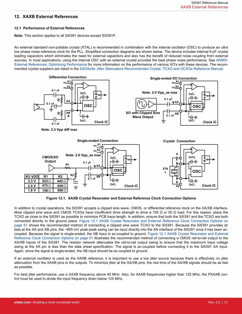
12. XAXB External References
12.1 Performance of External References
Note: This section applies to all Si5391 devices except Si5391P.
An external standard non-pullable crystal (XTAL) is recommended in combination with the internal oscillator (OSC) to produce an ultralow phase noise reference clock for the PLL. Simplified connection diagrams are shown below. The device includes internal 8 pF crystalloading capacitors which eliminates the need for external capacitors and also has the benefit of reduced noise coupling from externalsources. In most applications, using the internal OSC with an external crystal provides the best phase noise performance. See AN905:External References; Optimizing Performance for more information on the performance of various XO's with these devices. The recom-mended crystal suppliers are listed in the Si534x/8x Jitter Attenuators Recommended Crystal, TCXO and OCXOs Reference Manual.
Differential Connection
2xCL
2xCL
XB
XA
2xCL
2xCL
XB
XA
Single-ended XO Connection
Crystal Connection
OSC
XB
XA
XTAL
2xCL
2xCL
Clock IC
Clock IC Clock IC
Note: 2.0 Vpp_se max
XO with Clipped Sine Wave Output
2xCL
2xCL
XB
XAOSC
Clock IC
Note: 2.0 Vpp_se maxCMOS/XO Output
R2
R10.1 uf
0.1 uf
0.1 uf
0.1 uf
0.1 uf
0.1 uf0.1 uf
Single-ended Connection
Note: 2.5 Vpp diff max
X1
X2nc
nc
X1
X2ncnc
X1
X2nc
nc
X2
X1
OSCOSC0.1 uf
5050
XO VDD R1 R23.3 V
1.8 V2.5 V
523475158
442649866
Figure 12.1. XAXB Crystal Resonator and External Reference Clock Connection Options
In addition to crystal operations, the Si5391 accepts a clipped sine wave, CMOS, or differential reference clock on the XA/XB interface.Most clipped sine wave and CMOS TCXOs have insufficient drive strength to drive a 100 Ω or 50 Ω load. For this reason, place theTCXO as close to the Si5391 as possible to minimize PCB trace length. In addition, ensure that both the Si5391 and the TCXO are bothconnected directly to the ground plane. Figure 12.1 XAXB Crystal Resonator and External Reference Clock Connection Options onpage 51 shows the recommended method of connecting a clipped sine wave TCXO to the Si5391. Because the Si5391 provides dcbias at the XA and XB pins, the ~800 mV peak-peak swing can be input directly into the XA interface of the Si5391 once it has been ac-coupled. Because the signal is single-ended, the XB input is ac-coupled to ground. Figure 12.1 XAXB Crystal Resonator and ExternalReference Clock Connection Options on page 51 illustrates the recommended method of connecting a CMOS rail-to-rail output to theXA/XB inputs of the Si5391. The resistor network attenuates the rail-to-rail output swing to ensure that the maximum input voltageswing at the XA pin is less than the data sheet specification. The signal is ac-coupled before connecting it to the Si5391 XA input.Again, since the signal is single-ended, the XB input should be ac-coupled to ground.
If an external oscillator is used as the XAXB reference, it is important to use a low jitter source because there is effectively no jitterattenuation from the XAXB pins to the outputs. To minimize jitter at the XA/XB pins, the rise time of the XA/XB signals should be as fastas possible.
For best jitter performance, use a XAXB frequency above 40 MHz. Also, for XAXB frequencies higher than 125 MHz, the PXAXB con-trol must be used to divide the input frequency down below 125 MHz.
Si5391 Reference ManualXAXB External References
silabs.com | Building a more connected world. Rev. 0.2 | 51

12.2 Recommend Crystals and Oscillators
Refer to the Si534x/8x Jitter Attenuators Recommended Crystal, TCXO and OCXOs Reference Manual for more information.
12.3 Register Settings to Configure for External XTAL Reference
The following registers can be used to control and make adjustments for the external reference source used.
12.3.1 XAXB_EXTCLK_EN Reference Clock Selection Register
Table 12.1. XAXB External Clock Selection Register
Setting Name Hex Address [Bit Field] Function
Si5391/Si5391P
XAXB_EXTCLK_EN 090E[0] Selects between the XTAL or external reference clock on theXA/XB pins. Default is 0, XTAL. Set to 1 to use an external refer-ence oscillator. It must always be set to 0 (default) for Si5391P.
The internal crystal loading capacitors (CL) are disabled when an external clock source is selected.
12.3.2 PXAXB Pre-scale Divide Ratio for Reference Clock Register
Table 12.2. XAXB Pre-Scale Divide Ratio Register
Setting Name Hex Address [Bit Field] Function
Si5391/Si5391P
PXAXB 0x0206[1:0] Sets the XAXB input divider value according to the table below.
The following table lists the values, along with the corresponding divider ratio.
Table 12.3. XAXB Pre-Scale Divide Values
Value (Decimal) PXAXB Divider Value
0 1
1 2
2 4
3 8
Si5391 Reference ManualXAXB External References
silabs.com | Building a more connected world. Rev. 0.2 | 52
13. Crystal and Device Circuit Layout Recommendations
The main layout issues that should be carefully considered include the following:• Number and size of the ground vias for the Epad• Output clock trace routing• Input clock trace routing• Control and Status signals to input or output clock trace coupling• Xtal signal coupling• Xtal layout
If the application uses a crystal for the XAXB inputs a shield should be placed underneath the crystal connected to the X1 and X2 pinsto provide the best possible performance. The shield should not be connected to the ground plane(s), and the layers underneath shouldhave as little area under the shield as possible. It may be difficult to do this for all the layers, but it is important to do this for the layersthat are closest to the shield.
Go to the Silicon Labs Clock Development Tool webpage to obtain Si5391 evaluation board schematics, layouts, and component BOMfiles.
13.1 64-Pin QFN Si5391 Layout Recommendations
This section details the recommended guidelines for the crystal layout of the 64-pin Si5391 device using an example 8-layer PCB. Thefollowing are the descriptions of each of the eight layers.• Layer 1: device layer, with low speed CMOS control/status signals• Layer 2: crystal shield• Layer 3: ground plane• Layer 4: power distribution• Layer 5: power routing layer• Layer 6: input clocks• Layer 7: output clocks layer• Layer 8: ground layer
The 64 pin QFN crystal guidelines show the top layer layout of the Si5391 device mounted on the top PCB layer. This particular layoutwas designed to implement either a crystal or an external oscillator as the XAXB reference. The crystal/ oscillator area is outlined withthe white box around it. In this case, the top layer is flooded with ground. Note that this layout has a resistor in series with each pin ofthe crystal. In typical applications, these resistors should be removed.
13.1.1 Si5391 with an External Reference (Not Relevant to the Si5391P)
For devices that use an external reference like an XO, pins X1 and X2 should not be connected to "ground" and should be left as "no-connects". An external reference does not need a crystal shield or the voids underneath the shield. The XA/XB connection should betreated as a high speed critical path that is ac-coupled and terminated at the end of the etch run. The layout should minimize the straycapacitance from the XA pin to the XB pin. Jitter is very critical at the XA/XB pins and therefore split termination and differential signal-ing should be used whenever possible.
Si5391 Reference ManualCrystal and Device Circuit Layout Recommendations
silabs.com | Building a more connected world. Rev. 0.2 | 53

13.1.2 Si5391 Crystal Guidelines
The following are five recommended crystal guidelines:
1. Place the crystal as close as possible to the XA/XB pins.
2. DO NOT connect the crystal's GND pins to PCB gnd.
3. Connect the crystal's GND pins to the DUT's X1 and X2 pins via a local crystal GND shield placed around and under the crystal. SeeFigure 13.1 64-pin Si5391 Crystal Layout Recommendations Top Layer (Layer 1) on page 54 at the bottom left for an illustration ofhow to create a crystal GND shield by placing vias connecting the top layer traces to the shield layer underneath. Note that a zoomview of the crystal shield layer on the next layer down is shown in Figure 13.2 Zoom View Crystal Shield Layer, Below the Top Layer(Layer 2) on page 55.
4. Minimize traces adjacent to the crystal/oscillator area especially if they are clocks or frequently toggling digital signals.
5. In general do not route GND, power planes/traces, or locate components on the other side, below the crystal GND shield. As anexception if it is absolutely necessary to use the area on the other side of the board for layout or routing, then place the next referenceplane in the stack-up at least two layers away or at least 0.05 inches away. The Si5391 should have all layers underneath the groundshield removed if possible.
Figure 13.1. 64-pin Si5391 Crystal Layout Recommendations Top Layer (Layer 1)
Si5391 Reference ManualCrystal and Device Circuit Layout Recommendations
silabs.com | Building a more connected world. Rev. 0.2 | 54
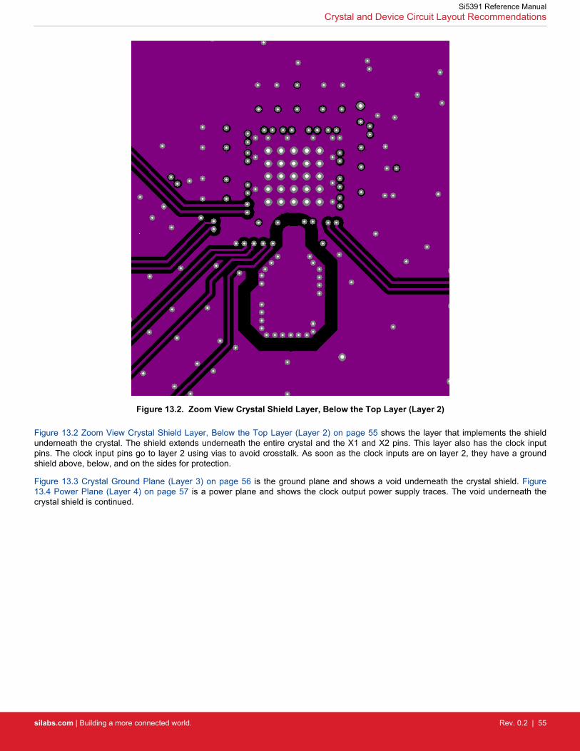
Figure 13.2. Zoom View Crystal Shield Layer, Below the Top Layer (Layer 2)
Figure 13.2 Zoom View Crystal Shield Layer, Below the Top Layer (Layer 2) on page 55 shows the layer that implements the shieldunderneath the crystal. The shield extends underneath the entire crystal and the X1 and X2 pins. This layer also has the clock inputpins. The clock input pins go to layer 2 using vias to avoid crosstalk. As soon as the clock inputs are on layer 2, they have a groundshield above, below, and on the sides for protection.
Figure 13.3 Crystal Ground Plane (Layer 3) on page 56 is the ground plane and shows a void underneath the crystal shield. Figure13.4 Power Plane (Layer 4) on page 57 is a power plane and shows the clock output power supply traces. The void underneath thecrystal shield is continued.
Si5391 Reference ManualCrystal and Device Circuit Layout Recommendations
silabs.com | Building a more connected world. Rev. 0.2 | 55

Figure 13.3. Crystal Ground Plane (Layer 3)
Si5391 Reference ManualCrystal and Device Circuit Layout Recommendations
silabs.com | Building a more connected world. Rev. 0.2 | 56
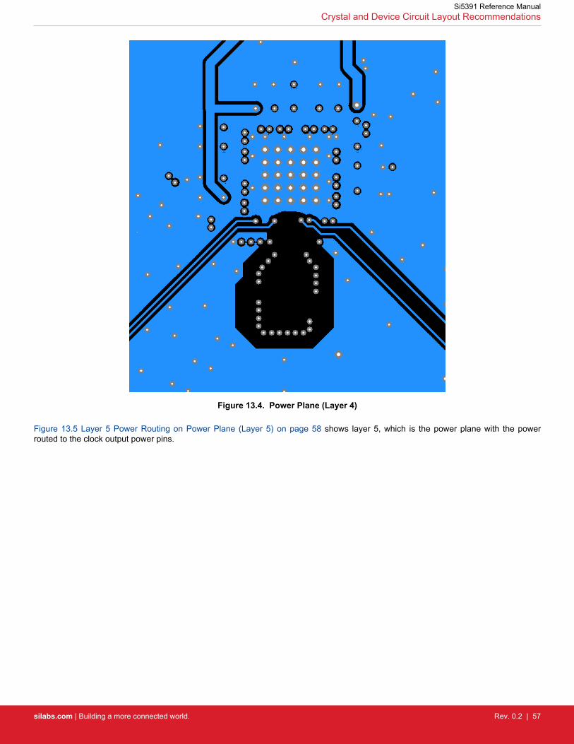
Figure 13.4. Power Plane (Layer 4)
Figure 13.5 Layer 5 Power Routing on Power Plane (Layer 5) on page 58 shows layer 5, which is the power plane with the powerrouted to the clock output power pins.
Si5391 Reference ManualCrystal and Device Circuit Layout Recommendations
silabs.com | Building a more connected world. Rev. 0.2 | 57
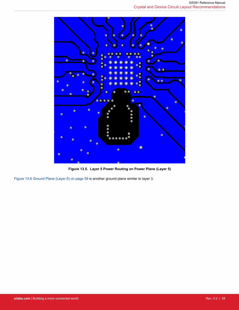
Figure 13.5. Layer 5 Power Routing on Power Plane (Layer 5)
Figure 13.6 Ground Plane (Layer 6) on page 59 is another ground plane similar to layer 3.
Si5391 Reference ManualCrystal and Device Circuit Layout Recommendations
silabs.com | Building a more connected world. Rev. 0.2 | 58

Figure 13.6. Ground Plane (Layer 6)
Si5391 Reference ManualCrystal and Device Circuit Layout Recommendations
silabs.com | Building a more connected world. Rev. 0.2 | 59

13.1.3 Si5391 Output Clocks
Figure 13.7 Output Clock Layer (Layer 7) on page 60 shows the output clocks. Similar to the input clocks the output clocks have viasthat immediately go to a buried layer with a ground plane above them and a ground flooded bottom layer. There is a ground floodingbetween the clock output pairs to avoid crosstalk. There should be a line of vias through the ground flood on either side of the outputclocks to ensure that the ground flood immediately next to the differential pairs has a low inductance path to the ground plane on layers3 and 6.
Figure 13.7. Output Clock Layer (Layer 7)
Si5391 Reference ManualCrystal and Device Circuit Layout Recommendations
silabs.com | Building a more connected world. Rev. 0.2 | 60

Figure 13.8. Bottom Layer Ground Flooded (Layer 8)
Si5391 Reference ManualCrystal and Device Circuit Layout Recommendations
silabs.com | Building a more connected world. Rev. 0.2 | 61

14. Power Management
14.1 Power Management Features
Several unused functions can be powered down to minimize power consumption. The registers listed below are used for poweringdown different features.
Table 14.1. Power-Down Registers
Register Name Hex Address [BitField]
Function
Si5391/Si5391P
PDN 0x001E[0] This bit allows powering down the device. The serial interface re-mains powered during power down mode.
OUT0A_PDN 0x0103[0] Powers down unused clock outputs.
OUT0_PDN 0x0108[0]
OUT1_PDN 0x010D[0]
OUT2_PDN 0x0112[0]
OUT3_PDN 0x0117[0]
OUT4_PDN 0x011C[0]
OUT5_PDN 0x0121[0]
OUT6_PDN 0x0126[0]
OUT7_PDN 0x012B[0]
OUT8_PDN 0x0130[0]
OUT9_PDN 0x0135[0]
OUT9A_PDN 0x013A[0]
OUT_PDN_ALL 0x0145[0] Power down all output drivers
XAXB_PDNB 0x090E[1] 0-Power down the oscillator and buffer circuitry at the XA/XB pins
1- No power down
14.2 Power Supply Recommendations
The power supply filtering generally is important for optimal timing performance. The Si5391/Si5391P devices have multiple stages ofon-chip regulation to minimize the impact of board level noise on clock jitter. Following conventional power supply filtering and layouttechniques will further minimize signal degradation from the power supply.
It is recommended to use a 1 μF 0402 ceramic capacitor on each VDD for optimal performance. It is also suggested to include an op-tional, single 0603 (resistor/ferrite) bead in series with each supply to enable additional filtering if needed.
Si5391 Reference ManualPower Management
silabs.com | Building a more connected world. Rev. 0.2 | 62

14.3 Power Supply Sequencing
Four classes of supply voltages exist on the Si5391/Si5391P:1. VDD = 1.8 V (Core digital supply)2. VDDA = 3.3 V (Analog supply)3. VDDOx = 1.8/2.5/3.3 V ± 5% (Clock output supply)4. VDDS = 1.8/3.3V ± 5% (Digital I/O supply)
There is no requirement for power supply sequencing unless the output clocks are required to be phase aligned with each other. In thiscase, the VDDO of each clock which needs to be aligned must be powered up before VDD and VDDA. VDDS has no effect on outputclock alignment.
If output-to-output alignment is required for applications where it is not possible to properly sequence the power supplies, then the out-put clocks can be aligned by asserting the SOFT_RST 0x001C[0] or Hard Reset 0x001E[1] register bits or driving the RSTB pin. Notethat using a hard reset will reload the register with the contents of the NVM and any unsaved changes will be lost.
One may observe that when powering up the VDD = 1.8 V rail first, that the VDDA = 3.3 V rail will initially follow the 1.8 V rail. Likewise,if the VDDA rail is powered down first then it will not drop far below VDD until VDD itself is powered down. This is due to the pad I/Ocircuits which have large MOSFET switches to select the local supply from either the VDD or VDDA rails. These devices are relativelylarge and yield a parasitic diode between VDD and VDDA. Please allow for both VDD and VDDA to power-up and power-down beforemeasuring their respective voltages.
14.4 Grounding Vias
The pad on the bottom of the device functions as both the sole electrical ground and primary heat transfer path. Hence it is important tominimize the inductance and maximize the heat transfer from this pad to the internal ground plane of the PCB. Use no fewer than 25vias from the center pad to a ground plane under the device. In general, more vias will perform better. Having the ground plane near thetop layer will also help to minimize the via inductance from the device to ground and maximize the heat transfer away from the device.
Si5391 Reference ManualPower Management
silabs.com | Building a more connected world. Rev. 0.2 | 63

15. Register Map
15.1 Base vs. Factory Preprogrammed Devices
The Si5391/Si5391P devices can be ordered as “base” or “factory-preprogrammed” (also known as “custom OPN”) versions.
15.2 “Base” Devices (a.k.a. “Blank” Devices)
Example “base” orderable part numbers (OPNs) are of the form “Si5391A-E-GM” or “Si5391B-E-GM”.
Base devices are available for applications where volatile reads and writes are used to program and configure the device for a particu-lar application.
Base devices do not power up in a usable state (all output clocks are disabled).
Base devices are, however, configured by default to use a 48 MHz crystal on the XA/XB reference and a 1.8 V compatible I/O voltagesetting for the host I2C/SPI interface.
Additional programming of a base device is mandatory to achieve a usable configuration.
See the on-line lookup utility at: www.silabs.com/products/clocksoscillators/clock-generator/Pages/clockbuilder-lookup.aspx to accessthe default configuration plan and register settings for any base OPN.
15.3 “Factory Preprogrammed” (Custom OPN) Devices
Factory preprogammed devices use a “custom OPN”, such as Si5391A-E-xxxxx-GM, where xxxxx is a sequence of characters as-signed by Silicon Labs for each customer-specific configuration. These characters are referred to as the “OPN ID”. Customers mustinitiate custom OPN creation using the ClockBuilder Pro software.
Many customers prefer to order devices which are factory preprogrammed for a particular application that includes specifying theXA/XB reference frequency/type, the clock input frequencies, the clock output frequencies, as well as the other options, such as auto-matic clock selection, loop BW, etc. The ClockBuilder software is required to select among all of these options and to produce a projectfile which Silicon Labs uses to preprogram all devices with custom orderable part number (“custom OPN”).
Custom OPN devices contain all of the initialization information in their non-volatile memory (NVM) so that it powers up fully configuredand ready to go.
Because preprogrammed device applications are inherently quite different from one another, the default power up values of the registersettings can be determined using the custom OPN utility at: www.silabs.com/products/clocksoscillators/clock-generator/Pages/clock-builder-lookup.aspx.
Custom OPN devices include a device top mark which includes the unique OPN ID. Refer to the device data sheet's Ordering Guideand Top Mark sections for more details.
Both “base” and “factory preprogrammed” devices can have their operating configurations changed at any time using volatile reads andwrites to the registers. Both types of devices can also have their current register configuration written to the NVM by executing an NVMbank burn sequence (see Section .)
Si5391 Reference ManualRegister Map
silabs.com | Building a more connected world. Rev. 0.2 | 64

15.4 Register Map Overview and Default Settings Values
The Si5391/Si5391P family parts have large register maps that are divided into separate “Pages” of register banks. This allows moreregister addresses than either the I2C or SPI serial interface standards 8-bit addressing provide. Each page has a maximum of 256addresses, however not all addresses are used on every page. Every register has a maximum data size of 8-bits, or 1 byte. Writing thepage number to the 8-bit serial interface address of 0x01 on any page (0x0001, 0x0101, 0x0201, etc.) updates the page selection forsubsequent register reads and writes. For example, to access the value in register 0x040E, it is first necessary to write the page value0x04 to serial interface register address 0x01. At this point, the value of serial interface address 0x0E (0x040E) may be read or written.Note that is it not necessary to write the page select register again when accessing other registers on the same page. Similarly, theread-only DEVICE_READY status is available from every page at serial interface address 0xFE (0x00FE, 0x01FE, 0x02FE, etc.).
It is recommended to use dynamic Read-Modify-Write methods when writing to registers which contain multiple settings, such as regis-ter 0x0011. To do this, first read the current contents of the register. Next, update only the select bit or bits that are being modified. Thismay involve using both logical AND and logical OR operations. Finally, write the updated contents back to the register. Writing to pa-ges, registers, or bits not documented below may cause undesired behavior in the device.
Details of the register and settings information are organized hierarchically below. To find the relevant information for your application,first choose the section corresponding to the base part number, Si5391 for your design. Then, choose the section under that for thepage containing the desired register(s).
Default register contents and settings differ for each device part number, or OPN. This information may be found by searching for theCustom OPN for your device using the link below. Both Base/Blank and Custom OPNs are available there. See the previous section on“Base vs. Factory Preprogrammed Devices" for more information on part numbers. The Private Addendum to the datasheet lists thedefault settings and frequency plan information. You must be logged into the Silicon Labs website to access this information. The Publicaddendum gives only the general frequency plan information (www.silabs.com/products/clocksoscillators/pages/clockbuilderlook-up.aspx).
Table 15.1. Register Map Paging Descriptions
Page Start Address (Hex) Start Address (Decimal) Contents
Page 0 0000h 0 Alarms, interrupts, reset, device ID, revision ID
Page 1 0100h 256 Clock output configuration
Page 2 0200h 512 P,R dividers, scratch area
Page 3 0300h 768 Output N dividers, N divider FINC/FDEC
Page 9 0900h 2304 Control IO configuration
R = Read Only
R/W = Read Write
S = Self Clearing
A self-clearing bit will be cleared by the device once the operation initiated by this bit is complete. Registers with “sticky” flag bits, suchas LOS0_FLG, are cleared by writing “0” to the bit that has been automatically set high by the device.
Si5391 Reference ManualRegister Map
silabs.com | Building a more connected world. Rev. 0.2 | 65

16. Si5391A/B Register Map
16.1 Page 0 Registers Si5391
Table 16.1. 0x0000 Die Rev
Reg Address Bit Field Type Setting Name Description
0x0000 3:0 R DIE_REV 4- bit Die Revision Number
0 = Silicon Revision A0
1 = Silicon Revision A1
Table 16.2. 0x0001 Page
Reg Address Bit Field Type Setting Name Description
0x0001 7:0 R/W PAGE Selects one of 256 possible pages.
There is the “Page Register” which is located at address 0x01 on every page. When read, it will indicate the current page. When writ-ten, it will change the page to the value entered. There is a page register at address 0x0001, 0x0101, 0x0201, 0x0301, … etc.
Table 16.3. 0x0002–0x0003 Base Part Number
Reg Address Bit Field Type Setting Name Description
0x0002 7:0 R PN_BASE Four-digit “base” part number, one nibble per digit
Example: Si5391A-A-GM. The base part number (OPN)is 5391, which is stored in this register
0x0003 15:8 R PN_BASE
Table 16.4. 0x0004 Device Speed/Synthesis Mode Grade
Reg Address Bit Field Type Setting Name Description
0x0004 7:0 R GRADE One ASCII character indicating the device speed grade:
0 = A
1 = B
2 = C
3 = D
Table 16.5. 0x0005 Device Revision
Reg Address Bit Field Type Setting Name Description
0x0005 7:0 R DEVICE_REV One ASCII character indicating the device revision lev-el:
0 = A; 1 = B
Example: in Si5391C-A12345-GM, the device revisionis “A” and is stored as 0.
Si5391 Reference ManualSi5391A/B Register Map
silabs.com | Building a more connected world. Rev. 0.2 | 66

Table 16.6. 0x0006–0x0008 Tool Version
Reg Address Bit Field Type Setting Name Description
0x0006 3:0 R TOOL_VERSION[3:0] Special
0x0006 7:4 R TOOL_VERSION[7:4] Revision
0x0007 7:0 R TOOL_VERSION[15:8] Minor[7:0]
0x0008 0 R TOOL_VERSION[15:8] Minor[8]
0x0008 4:1 R TOOL_VERSION[16] Major
0x0008 7:5 R TOOL_VERSION[13:17] Tool. 0 for Clockbuilder Pro.
Table 16.7. 0x0009 Temperature Grade
Reg Address Bit Field Type Setting Name Description
0x0009 7:0 R TEMP_GRADE Device temperature grading
0 = Industrial (–40 ° C to 85 ° C) ambient conditions
Table 16.8. 0x000A Package ID
Reg Address Bit Field Type Setting Name Description
0x000A 7:0 R PKG_ID Package ID
0 = 9x9 mm 64 QFN
1 = 7x7 mm 44 QFN
Part numbers are of the form:
Si<Part Num Base><Grade>-<Device Revision><OPN ID>-<Temp Grade><Package ID>
Examples:
Si5391C-A12345-GM
Applies to a “custom” OPN (Ordering Part Number) device. These devices are factory pre-programmed with the frequency plan and allother operating characteristics defined by the user’s ClockBuilder Pro project file.
Si5391C-A-GM
Applies to a “base” or “blank” OPN device. Base devices are factory pre-programmed to a specific base part type (e.g., Si5391 butexclude any user-defined frequency plan or other user-defined operating characteristics selected in ClockBuilder Pro.
Table 16.9. 0x000B I2C Address
Reg Address Bit Field Type Setting Name Description
0x000B 6:2 R/W I2C_ADDR The upper 5 bits of the 7-bit I2C address.
The lower 2 bits are controlled by the A1 and A0 pins.
Table 16.10. 0x000C Status Bits
Reg Address Bit Field Type Setting Name Description
0x000C 0 R SYSINCAL 1 if the device is calibrating.
Si5391 Reference ManualSi5391A/B Register Map
silabs.com | Building a more connected world. Rev. 0.2 | 67

Reg Address Bit Field Type Setting Name Description
0x000C 1 R LOSXAXB 1 if there is no signal at the XA pin as the LOS detectoris only connected to the XA pin.
0x000C 2 R LOSREF 1 if the Phase Frequency detector does not have a sig-nal from XAXB, IN2, IN1, or IN0.
0x000C 3 R LOL 1 if the DSPLL is out of lock.
0x000C 5 R SMBUS_TIMEOUT 1 if there is an SMBus timeout error.
Table 16.11. 0x000D INx Loss of Signal (LOS) Alarms
Reg Address Bit Field Type Setting Name Description
0x000D 3:0 R LOSIN 1 if no clock is present at [FB_IN, IN2, IN1, IN0]
Note that each bit corresponds to the input. The LOS bits are not sticky.• Input 0 (IN0) corresponds to LOS at 0x000D [0]• Input 1 (IN1) corresponds to LOS at 0x000D [1]• Input 2 (IN2) corresponds to LOS at 0x000D [2]• FB_IN corresponds to LOS at 0x000D[3]• See also LOSXAXB for LOS at the XAXB input
Table 16.12. 0x0011 Sticky Versions of Status Bits
Reg Address Bit Field Type Setting Name Description
0x0011 0 R SYSINCAL_FLG Sticky version of SYSINCAL. Write a 0 to clear theflag.
0x0011 1 R LOSXAXB_FLG Sticky version of LOSXAXB. Write a 0 to clear theflag.
0x0011 2 R LOSREF_FLG Sticky version of LOSREF. Write a 0 to clear theflag.
0x0011 3 R LOL_FLG Sticky version of LOL. Write a 0 to clear the flag.
0x0011 5 R SMBUS_TIMEOUT_FLG Sticky version of SMBUS_TIMEOUT. Write a 0 toclear the flag.
Table 16.13. 0x0012 INx LOS Flags
Reg Address Bit Field Type Setting Name Description
0x0012 3:0 R/W LOSIN_FLG Sticky version of LOS. Write a 0 to clear each individualflag.
Table 16.14. 0x0017 Status Flag Interrupt Masks
Reg Address Bit Field Type Setting Name Description
0x0017 0 R/W SYSINCAL_INTR_MSK 1 to mask SYSINCAL_FLG from causing an interrupt
0x0017 1 R/W LOSXAXB_INTR_MSK 1 to mask the LOSXAXB_FLG from causing an interrupt
0x0017 2 R/W LOSREF_INTR_MSK 1 to mask LOSREF_FLG from causing an interrupt
0x0017 3 R/W LOL_INTR_MSK 1 to mask LOL_FLG from causing an interrupt
Si5391 Reference ManualSi5391A/B Register Map
silabs.com | Building a more connected world. Rev. 0.2 | 68
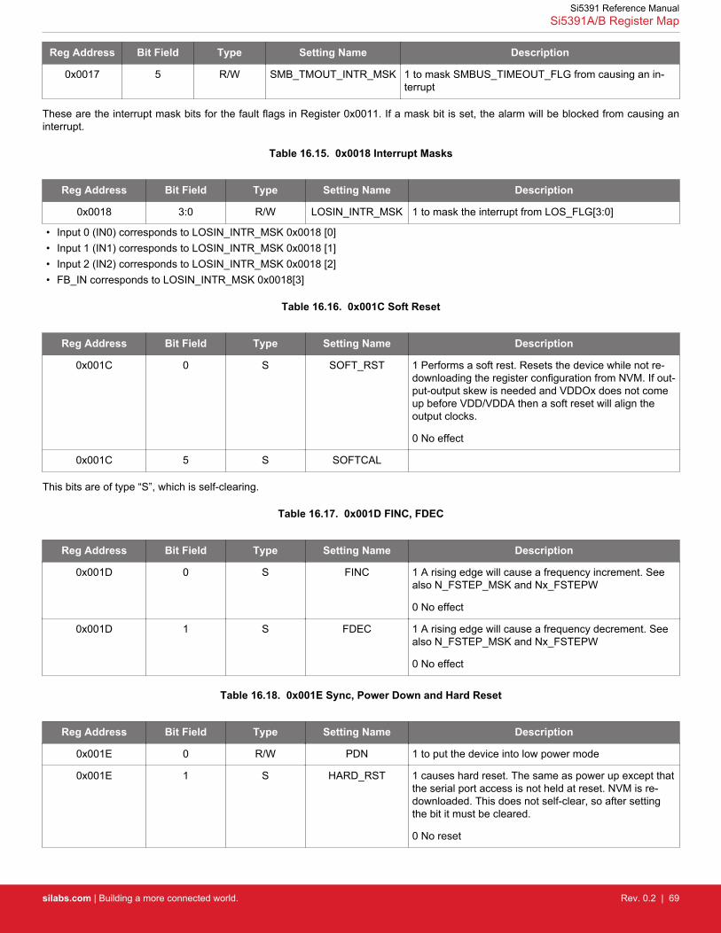
Reg Address Bit Field Type Setting Name Description
0x0017 5 R/W SMB_TMOUT_INTR_MSK 1 to mask SMBUS_TIMEOUT_FLG from causing an in-terrupt
These are the interrupt mask bits for the fault flags in Register 0x0011. If a mask bit is set, the alarm will be blocked from causing aninterrupt.
Table 16.15. 0x0018 Interrupt Masks
Reg Address Bit Field Type Setting Name Description
0x0018 3:0 R/W LOSIN_INTR_MSK 1 to mask the interrupt from LOS_FLG[3:0]
• Input 0 (IN0) corresponds to LOSIN_INTR_MSK 0x0018 [0]• Input 1 (IN1) corresponds to LOSIN_INTR_MSK 0x0018 [1]• Input 2 (IN2) corresponds to LOSIN_INTR_MSK 0x0018 [2]• FB_IN corresponds to LOSIN_INTR_MSK 0x0018[3]
Table 16.16. 0x001C Soft Reset
Reg Address Bit Field Type Setting Name Description
0x001C 0 S SOFT_RST 1 Performs a soft rest. Resets the device while not re-downloading the register configuration from NVM. If out-put-output skew is needed and VDDOx does not comeup before VDD/VDDA then a soft reset will align theoutput clocks.
0 No effect
0x001C 5 S SOFTCAL
This bits are of type “S”, which is self-clearing.
Table 16.17. 0x001D FINC, FDEC
Reg Address Bit Field Type Setting Name Description
0x001D 0 S FINC 1 A rising edge will cause a frequency increment. Seealso N_FSTEP_MSK and Nx_FSTEPW
0 No effect
0x001D 1 S FDEC 1 A rising edge will cause a frequency decrement. Seealso N_FSTEP_MSK and Nx_FSTEPW
0 No effect
Table 16.18. 0x001E Sync, Power Down and Hard Reset
Reg Address Bit Field Type Setting Name Description
0x001E 0 R/W PDN 1 to put the device into low power mode
0x001E 1 S HARD_RST 1 causes hard reset. The same as power up except thatthe serial port access is not held at reset. NVM is re-downloaded. This does not self-clear, so after settingthe bit it must be cleared.
0 No reset
Si5391 Reference ManualSi5391A/B Register Map
silabs.com | Building a more connected world. Rev. 0.2 | 69

Reg Address Bit Field Type Setting Name Description
0x001E 2 S SYNC Logically equivalent to asserting the SYNC pin. Resetsall R dividers so that synchronous output frequencieswill be aligned.
Table 16.19. 0x0021 Input Clock Selection
Reg Address Bit Field Type Setting Name Description
0x0021 0 R/W IN_SEL_REGCTRL Selects between register controlled reference clock se-lection and pin controlled clock selection using IN_SEL1and IN_SEL0 pins: 0 for pin controlled clock selection; 1for register clock selection via IN_SEL bits.
0x0021 2:1 R/W IN_SEL Selects the reference clock input to the PLL whenIN_SEL_REGCTRL=1.
0 IN0
1 IN1
2 IN2
3 XA/XB
Table 16.20. 0x002B SPI 3 vs. 4 Wire
Reg Address Bit Field Type Setting Name Description
0x002B 3 R/W SPI_3WIRE 0 for 4-wire SPI, 1 for 3-wire SPI
Table 16.21. 0x002C LOS Enable
Reg Address Bit Field Type Setting Name Description
0x002C 3:0 R/W LOS_EN 1 to enable LOS for the inputs other than XAXB;
0 for disable
0x002C 4 R/W LOSXAXB_DIS 1 to disable LOS for the XAXB input
• Input 0 (IN0): LOS_EN[0]• Input 1 (IN1): LOS_EN[1]• Input 2 (IN2): LOS_EN[2]• FB_IN: LOS_EN[3]
Table 16.22. 0x002D Loss of Signal Requalification Time
Reg Address Bit Field Type Setting Name Description
0x002D 1:0 R/W LOS0_VAL_TIME Clock Input 0
0 for 2 msec
1 for 100 msec
2 for 200 msec
3 for one second
0x002D 3:2 R/W LOS1_VAL_TIME Clock Input 1, same as above
0x002D 5:4 R/W LOS2_VAL_TIME Clock Input 2, same as above
Si5391 Reference ManualSi5391A/B Register Map
silabs.com | Building a more connected world. Rev. 0.2 | 70

Reg Address Bit Field Type Setting Name Description
0x002D 7:6 R/W LOS3_VAL_TIME Clock Input 3, same as above
When an input clock is gone (and therefore has an active LOS alarm), if the clock returns, there is a period of time that the clock mustbe within the acceptable range before the alarm is removed. This is the LOS_VAL_TIME.
Table 16.23. 0x002E–0x002F LOS0 Trigger Threshold
Reg Address Bit Field Type Setting Name Description
0x002E 7:0 R/W LOS0_TRG_THR 16-bit Threshold Value
0x002F 15:8 R/W LOS0_TRG_THR
ClockBuilder Pro calculates the correct LOS register threshold trigger value for Input 0, given a particular frequency plan.
Table 16.24. 0x0030–0x0031 LOS1 Trigger Threshold
Reg Address Bit Field Type Setting Name Description
0x0030 7:0 R/W LOS1_TRG_THR 16-bit Threshold Value
0x0031 15:8 R/W LOS1_TRG_THR
ClockBuilder Pro calculates the correct LOS register threshold trigger value for Input 1, given a particular frequency plan.
Table 16.25. 0x0032–0x0033 LOS2 Trigger Threshold
Reg Address Bit Field Type Setting Name Description
0x0032 7:0 R/W LOS2_TRG_THR 16-bit Threshold Value
0x0033 15:8 R/W LOS2_TRG_THR
ClockBuilder Pro calculates the correct LOS register threshold trigger value for Input 2, given a particular frequency plan.
Table 16.26. 0x0034–0x0035 LOS3 Trigger Threshold
Reg Address Bit Field Type Setting Name Description
0x0034 7:0 R/W LOS3_TRG_THR 16-bit Threshold Value
0x0035 15:8 R/W LOS3_TRG_THR
ClockBuilder Pro calculates the correct LOS register threshold trigger value for Input 3, given a particular frequency plan.
Table 16.27. 0x0036–0x0037 LOS0 Clear Threshold
Reg Address Bit Field Type Setting Name Description
0x0036 7:0 R/W LOS0_CLR_THR 16-bit Threshold Value
0x0037 15:8 R/W LOS0_CLR_THR
ClockBuilder Pro calculates the correct LOS register clear threshold value for Input 0, given a particular frequency plan.
Si5391 Reference ManualSi5391A/B Register Map
silabs.com | Building a more connected world. Rev. 0.2 | 71

Table 16.28. 0x0038–0x0039 LOS1 Clear Threshold
Reg Address Bit Field Type Setting Name Description
0x0038 7:0 R/W LOS1_CLR_THR 16-bit Threshold Value
0x0039 15:8 R/W LOS1_CLR_THR
ClockBuilder Pro calculates the correct LOS register clear threshold value for Input 1, given a particular frequency plan.
Table 16.29. 0x003A–0x003B LOS2 Clear Threshold
Reg Address Bit Field Type Setting Name Description
0x003A 7:0 R/W LOS2_CLR_THR 16-bit Threshold Value
0x003B 15:8 R/W LOS2_CLR_THR
ClockBuilder Pro calculates the correct LOS register clear threshold value for Input 2, given a particular frequency plan.
Table 16.30. 0x003C–0x003D LOS3 Clear Threshold
Reg Address Bit Field Type Setting Name Description
0x003C 7:0 R/W LOS3_CLR_THR 16-bit Threshold Value
0x003D 15:8 R/W LOS3_CLR_THR
ClockBuilder Pro calculates the correct LOS register clear threshold value for Input 3, given a particular frequency plan.
Table 16.31. 0x0041–0x0044 LOS Pre-Divider for IN0, IN1, IN3, FB_IN
Reg Address Bit Field Type Setting Name Description
0x0041 7:0 R/W LOS0_DIV_SEL A pre-divider that is configured by ClockBuilder Pro
0x0042 7:0 R/W LOS1_DIV_SEL A pre-divider that is configured by ClockBuilder Pro
0x0043 7:0 R/W LOS2_DIV_SEL A pre-divider that is configured by ClockBuilder Pro
0x0044 7:0 R/W LOS3_DIV_SEL A pre-divider that is configured by ClockBuilder Pro
The following are the pre-divider values for the above-listed registers values.
Si5391 Reference ManualSi5391A/B Register Map
silabs.com | Building a more connected world. Rev. 0.2 | 72
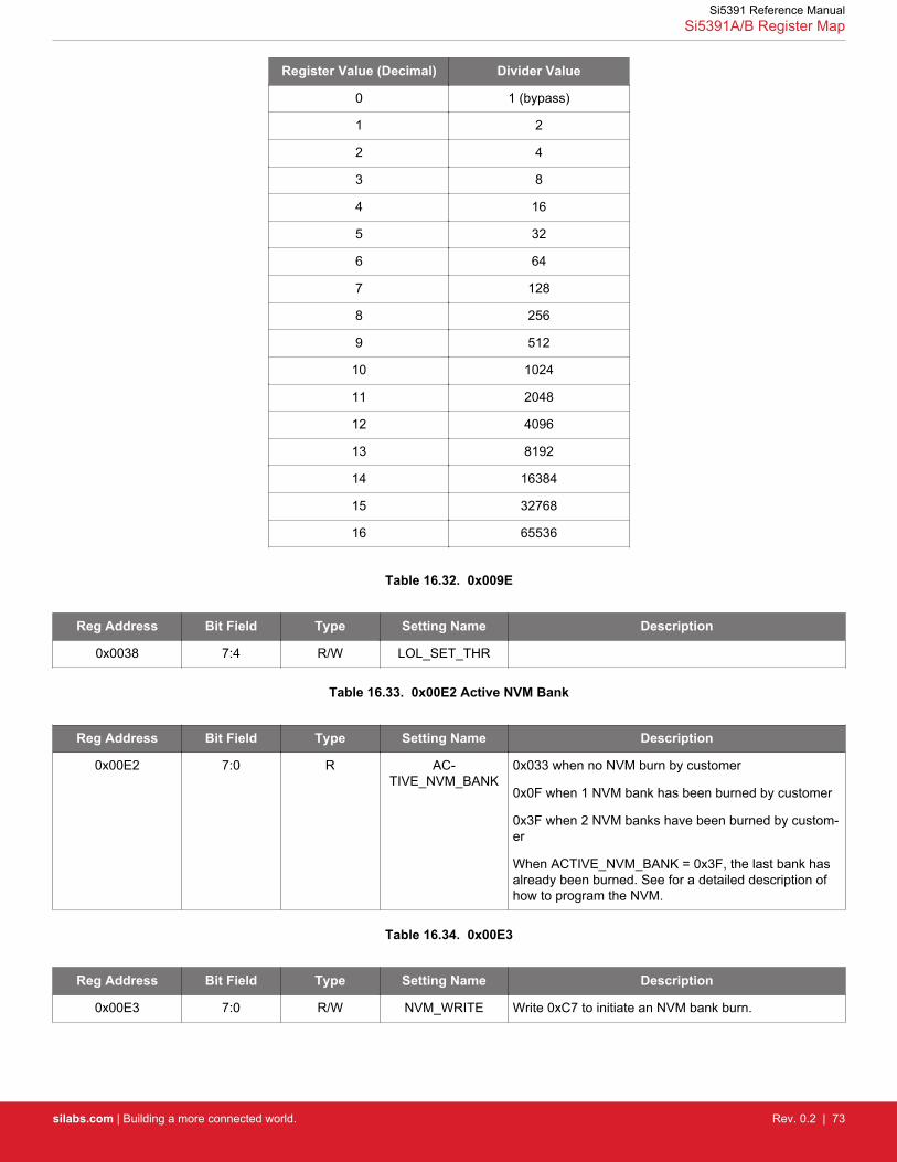
Register Value (Decimal) Divider Value
0 1 (bypass)
1 2
2 4
3 8
4 16
5 32
6 64
7 128
8 256
9 512
10 1024
11 2048
12 4096
13 8192
14 16384
15 32768
16 65536
Table 16.32. 0x009E
Reg Address Bit Field Type Setting Name Description
0x0038 7:4 R/W LOL_SET_THR
Table 16.33. 0x00E2 Active NVM Bank
Reg Address Bit Field Type Setting Name Description
0x00E2 7:0 R AC-TIVE_NVM_BANK
0x033 when no NVM burn by customer
0x0F when 1 NVM bank has been burned by customer
0x3F when 2 NVM banks have been burned by custom-er
When ACTIVE_NVM_BANK = 0x3F, the last bank hasalready been burned. See for a detailed description ofhow to program the NVM.
Table 16.34. 0x00E3
Reg Address Bit Field Type Setting Name Description
0x00E3 7:0 R/W NVM_WRITE Write 0xC7 to initiate an NVM bank burn.
Si5391 Reference ManualSi5391A/B Register Map
silabs.com | Building a more connected world. Rev. 0.2 | 73

Table 16.35. 0x00E4
Reg Address Bit Field Type Setting Name Description
0x00E4 0 S NVM_READ_BANK When set, this bit will read the NVM down into the vola-tile memory.
Table 16.36. 0x00F6
Reg Address Bit Field Type Setting Name Description
0x00F6 0 R/W REG_0XF7_INTR
0x00F6 1 R/W REG_0XF8_INTR
0x00F6 2 R/W REG_0XF9_INTR
Table 16.37. 0x00F7
Reg Address Bit Field Type Setting Name Description
0x00F7 0 R/W SYSINCAL_INTR
0x00F7 1 R/W LOSXAXB_INTR
0x00F7 2 R/W LOSREF_INTR
0x00F7 3 R/W LOL_INTR
0x00F7 4 R/W LOSVCO_INTR
0x00F7 5 R/W SMBUS_TIME_OUT_
INTR
Table 16.38. 0x00F8
Reg Address Bit Field Type Setting Name Description
0x00F8 3:0 R/W LOS_INTR
Table 16.39. 0x00F9
Reg Address Bit Field Type Setting Name Description
0x00F9 0 R/W LOL_INTR_PLLA
0x00F9 1 R/W LOL_INTR_PLLB
0x00F9 2 R/W LOL_INTR_PLLC
0x00F9 3 R/W LOL_INTR_PLLD
0x00F9 4 R/W HOLD_INTR_PLLA
0x00F9 5 R/W HOLD_INTR_PLLB
0x00F9 6 R/W HOLD_INTR_PLLC
0x00F9 7 R/W HOLD_INTR_PLLD
Si5391 Reference ManualSi5391A/B Register Map
silabs.com | Building a more connected world. Rev. 0.2 | 74

16.2 Page 1 Registers Si5391
Table 16.40. 0x0102 All Output Clock Driver Disable
Reg Address Bit Field Type Setting Name Description
0x0102 0 R/W OUTALL_DISA-BLE_LOW
0: Disables all output drivers.
1: No output drivers are disabled by this bit, but othersignals may disable the outputs.
Table 16.41. 0x0108 Clock Output 0 Configs and DIV2 Mode
Reg Address Bit Field Type Setting Name Description
0x0108 0 R/W OUT0_PDN Output driver 0: 0 to power up the driver, 1 to powerdown the driver. Clock outputs will be weakly pulled-low.
0x0108 1 R/W OUT0_OE Output driver 0: 0 to disable the output, 1 to enable theoutput
0x0108 2 R/W OUT0_RDIV_FORCE2
0 R0 divider value is set by R0_REG
1 R0 divider value is forced into divide by 2
Table 16.42. 0x0109 Clock Output 0 Format
Reg Address Bit Field Type Setting Name Description
0x0109 2:0 R/W OUT0_FORMAT 0: Reserved
1: normal differential
2: low power differential
3: reserved
4: LVCMOS
5–7: Reserved
0x0109 3 R/W OUT0_SYNC_EN 0 disable
1: Enable
Enable/disable synchronized (glitchless) operation.When enabled, the power down and output enables aresynchronized to the output clock.
0x0109 5:4 R/W OUT0_DIS_STATE Determines the state of an output driver when disabled,selectable as:
0: Disable in low state
1: Disable in high state
2: Reserved
3: Reserved
0x0109 7:6 R/W OUT0_CMOS_DRV LVCMOS output impedance. See 8.4.8 Output DriverSettings for LVPECL, LVDS, HCSL, and CML.
See 8.3 Performance Guidelines for Outputs.
Si5391 Reference ManualSi5391A/B Register Map
silabs.com | Building a more connected world. Rev. 0.2 | 75
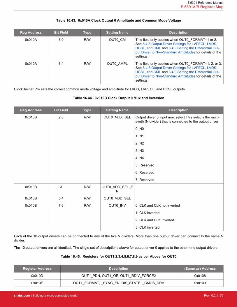
Table 16.43. 0x010A Clock Output 0 Amplitude and Common Mode Voltage
Reg Address Bit Field Type Setting Name Description
0x010A 3:0 R/W OUT0_CM This field only applies when OUT0_FORMAT=1 or 2.See 8.4.8 Output Driver Settings for LVPECL, LVDS,HCSL, and CML and 8.4.9 Setting the Differential Out-put Driver to Non-Standard Amplitudes for details of thesettings.
0x010A 6:4 R/W OUT0_AMPL This field only applies when OUT0_FORMAT=1, 2, or 3.See 8.4.8 Output Driver Settings for LVPECL, LVDS,HCSL, and CML and 8.4.9 Setting the Differential Out-put Driver to Non-Standard Amplitudes for details of thesettings.
ClockBuilder Pro sets the correct common mode voltage and amplitude for LVDS, LVPECL, and HCSL outputs.
Table 16.44. 0x010B Clock Output 0 Mux and Inversion
Reg Address Bit Field Type Setting Name Description
0x010B 2:0 R/W OUT0_MUX_SEL Output driver 0 input mux select.This selects the multi-synth (N divider) that is connected to the output driver.
0: N0
1: N1
2: N2
3: N3
4: N4
5: Reserved
6: Reserved
7: Reserved
0x010B 3 R/W OUT0_VDD_SEL_EN
0x010B 5:4 R/W OUT0_VDD_SEL
0x010B 7:6 R/W OUT0_INV 0: CLK and CLK not inverted
1: CLK inverted
2: CLK and CLK inverted
3: CLK inverted
Each of the 10 output drivers can be connected to any of the five N dividers. More than one output driver can connect to the same Ndivider.
The 10 output drivers are all identical. The single set of descriptions above for output driver 0 applies to the other nine output drivers.
Table 16.45. Registers for OUT1,2,3,4,5,6,7,8,9 as per Above for OUT0
Register Address Description (Same as) Address
0x010D OUT1_PDN, OUT1_OE, OUT1_RDIV_FORCE2 0x0108
0x010E OUT1_FORMAT, _SYNC_EN, DIS_STATE, _CMOS_DRV 0x0109
Si5391 Reference ManualSi5391A/B Register Map
silabs.com | Building a more connected world. Rev. 0.2 | 76

Register Address Description (Same as) Address
0x010F OUT1_CM, OUT1_AMPL 0x010A
0x0110 OUT1_MUX_SEL, OUT1_VDD_SEL_EN, OUT1_VDD_SEL, OUT1_INV 0x010B
0x0112 OUT2_PDN, OUT2_OE, OUT2_RDIV_FORCE2 0x0108
0x0113 OUT2_FORMAT, _SYNC_EN, DIS_STATE, _CMOS_DRV 0x0109
0x0114 OUT2_CM, OUT2_AMPL 0x010A
0x0115 OUT2_MUX_SEL, OUT2_VDD_SEL_EN, OUT2_VDD_SEL, OUT2_INV 0x010B
0x0117 OUT3_PDN, OUT3_OE, OUT3_RDIV_FORCE2 0x0108
0x0118 OUT3_FORMAT, _SYNC_EN, DIS_STATE, _CMOS_DRV 0x0109
0x0119 OUT3_CM, OUT3_AMPL 0x010A
0x011A OUT3_MUX_SEL, OUT3_VDD_SEL_EN, OUT3_VDD_SEL, OUT3_INV 0x010B
0x011C OUT4_PDN, OUT4_OE, OUT4_RDIV_FORCE2 0x0108
0x011D OUT4_FORMAT, _SYNC_EN, DIS_STATE, _CMOS_DRV 0x010A
0x011E OUT4_CM, OUT4_AMPL 0x0105
0x011F OUT4_MUX_SEL, OUT4_VDD_SEL_EN, OUT4_VDD_SEL, OUT4_INV 0x010B
0x0121 OUT5_PDN, OUT5_OE, OUT5_RDIV_FORCE2 0x0108
0x0122 OUT5_FORMAT, _SYNC_EN, DIS_STATE, _CMOS_DRV 0x0109
0x0123 OUT5_CM, OUT5_AMPL 0x010A
0x0124 OUT5_MUX_SEL, OUT5_VDD_SEL_EN, OUT5_VDD_SEL, OUT5_INV 0x010B
0x0126 OUT6_PDN, OUT6_OE, OUT6_RDIV_FORCE2 0x0108
0x0127 OUT6_FORMAT, _SYNC_EN, DIS_STATE, _CMOS_DRV 0x010A
0x0128 OUT6_CM, OUT6_AMPL 0x0109
0x0129 OUT6_MUX_SEL, OUT6_VDD_SEL_EN, OUT6_VDD_SEL, OUT6_INV 0x010B
0x012B OUT7_PDN, OUT7_OE, OUT7_RDIV_FORCE2 0x0108
0x012C OUT7_FORMAT, _SYNC_EN, DIS_STATE, _CMOS_DRV 0x0109
0x012D OUT7_CM, OUT7_AMPL 0x010A
0x012E OUT7_MUX_SEL, OUT7_VDD_SEL_EN, OUT7_VDD_SEL, OUT7_INV 0x010B
0x0130 OUT8_PDN, OUT8_OE, OUT8_RDIV_FORCE2 0x0108
0x0131 OUT8_FORMAT, _SYNC_EN, DIS_STATE, _CMOS_DRV 0x0109
0x0132 OUT8_CM, OUT8_AMPL 0x010A
0x0133 OUT8_MUX_SEL, OUT8_VDD_SEL_EN, OUT8_VDD_SEL, OUT8_INV 0x010B
0x013A OUT9_PDN, OUT9_OE, OUT9_RDIV_FORCE2 0x0108
0x013B OUT9_FORMAT, _SYNC_EN, DIS_STATE, _CMOS_DRV 0x0109
0x013C OUT9_CM, OUT9_AMPL 0x010A
0x013D OUT9_MUX_SEL, OUT9_VDD_SEL_EN, OUT9_VDD_SEL, OUT9_INV 0x010B
Si5391 Reference ManualSi5391A/B Register Map
silabs.com | Building a more connected world. Rev. 0.2 | 77
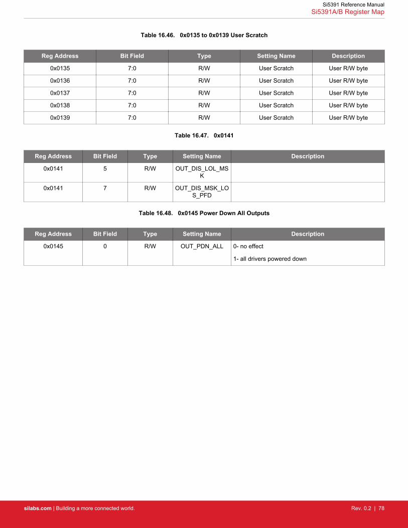
Table 16.46. 0x0135 to 0x0139 User Scratch
Reg Address Bit Field Type Setting Name Description
0x0135 7:0 R/W User Scratch User R/W byte
0x0136 7:0 R/W User Scratch User R/W byte
0x0137 7:0 R/W User Scratch User R/W byte
0x0138 7:0 R/W User Scratch User R/W byte
0x0139 7:0 R/W User Scratch User R/W byte
Table 16.47. 0x0141
Reg Address Bit Field Type Setting Name Description
0x0141 5 R/W OUT_DIS_LOL_MSK
0x0141 7 R/W OUT_DIS_MSK_LOS_PFD
Table 16.48. 0x0145 Power Down All Outputs
Reg Address Bit Field Type Setting Name Description
0x0145 0 R/W OUT_PDN_ALL 0- no effect
1- all drivers powered down
Si5391 Reference ManualSi5391A/B Register Map
silabs.com | Building a more connected world. Rev. 0.2 | 78
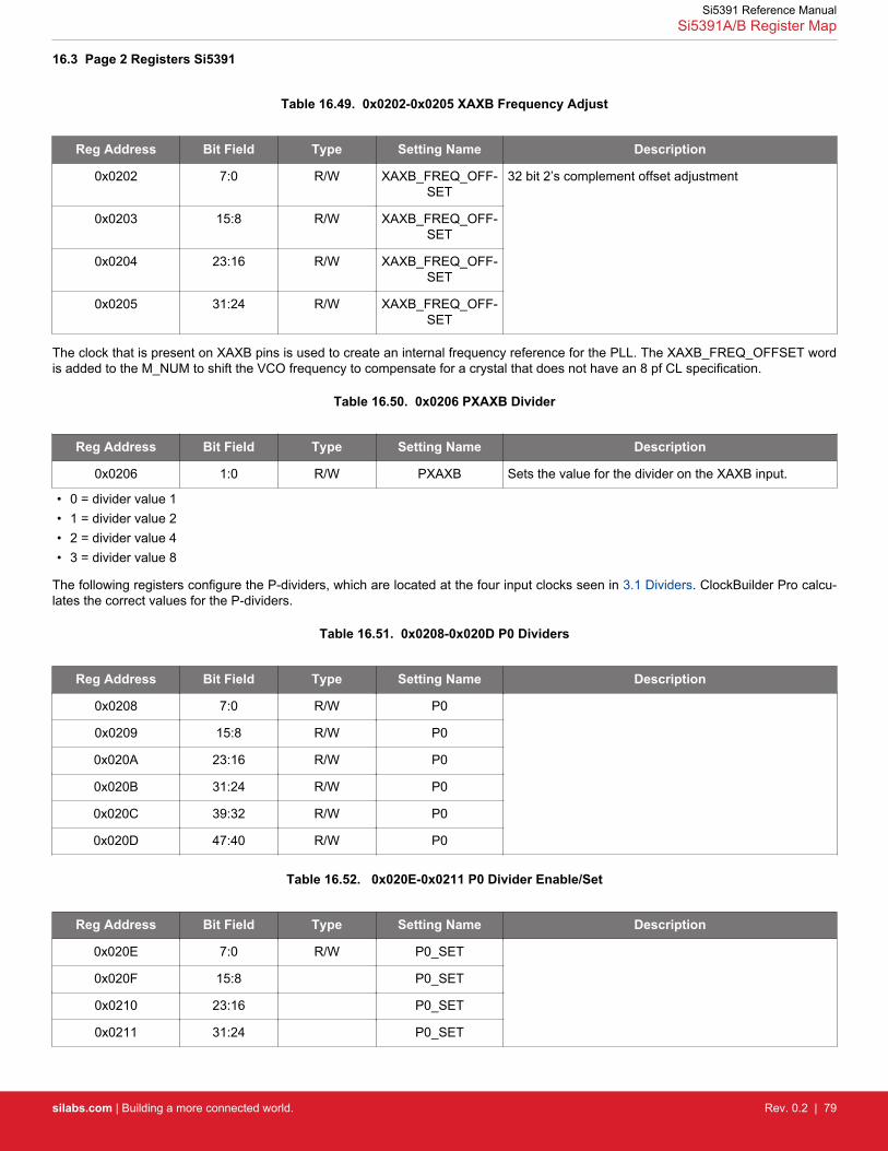
16.3 Page 2 Registers Si5391
Table 16.49. 0x0202-0x0205 XAXB Frequency Adjust
Reg Address Bit Field Type Setting Name Description
0x0202 7:0 R/W XAXB_FREQ_OFF-SET
32 bit 2’s complement offset adjustment
0x0203 15:8 R/W XAXB_FREQ_OFF-SET
0x0204 23:16 R/W XAXB_FREQ_OFF-SET
0x0205 31:24 R/W XAXB_FREQ_OFF-SET
The clock that is present on XAXB pins is used to create an internal frequency reference for the PLL. The XAXB_FREQ_OFFSET wordis added to the M_NUM to shift the VCO frequency to compensate for a crystal that does not have an 8 pf CL specification.
Table 16.50. 0x0206 PXAXB Divider
Reg Address Bit Field Type Setting Name Description
0x0206 1:0 R/W PXAXB Sets the value for the divider on the XAXB input.
• 0 = divider value 1• 1 = divider value 2• 2 = divider value 4• 3 = divider value 8
The following registers configure the P-dividers, which are located at the four input clocks seen in 3.1 Dividers. ClockBuilder Pro calcu-lates the correct values for the P-dividers.
Table 16.51. 0x0208-0x020D P0 Dividers
Reg Address Bit Field Type Setting Name Description
0x0208 7:0 R/W P0
0x0209 15:8 R/W P0
0x020A 23:16 R/W P0
0x020B 31:24 R/W P0
0x020C 39:32 R/W P0
0x020D 47:40 R/W P0
Table 16.52. 0x020E-0x0211 P0 Divider Enable/Set
Reg Address Bit Field Type Setting Name Description
0x020E 7:0 R/W P0_SET
0x020F 15:8 P0_SET
0x0210 23:16 P0_SET
0x0211 31:24 P0_SET
Si5391 Reference ManualSi5391A/B Register Map
silabs.com | Building a more connected world. Rev. 0.2 | 79

Table 16.53. 0x0212-0x0217 P1 Dividers
Reg Address Bit Field Type Setting Name Description
0x0212 7:0 R/W P1
0x0213 15:8 R/W P1
0x0214 23:16 R/W P1
0x0215 31:24 R/W P1
0x0216 39:32 R/W P1
0x0217 47:40 R/W P1
Table 16.54. 0x0218-0x021B P1 Divider Enable/Set
Reg Address Bit Field Type Setting Name Description
0x0218 7:0 R/W P1_SET
0x0219 15:8 P1_SET
0x021A 23:16 P1_SET
0x021B 31:24 P1_SET
Table 16.55. 0x021C-0x0221 P2 Dividers
Reg Address Bit Field Type Setting Name Description
0x021C 7:0 R/W P2
0x021D 15:8 R/W P2
0x021E 23:16 R/W P2
0x021F 31:24 R/W P2
0x0220 39:32 R/W P2
0x0221 47:40 R/W P2
Table 16.56. 0x0222-0x0225 P2 Divider Enable/Set
Reg Address Bit Field Type Setting Name Description
0x0222 7:0 R/W P2_SET
0x0223 15:8 P2_SET
0x0224 23:16 P2_SET
0x0225 31:24 P2_SET
Table 16.57. 0x0226-0x022B P3 Dividers
Reg Address Bit Field Type Setting Name Description
0x0226 7:0 R/W P3
0x0227 15:8 R/W P3
Si5391 Reference ManualSi5391A/B Register Map
silabs.com | Building a more connected world. Rev. 0.2 | 80

Reg Address Bit Field Type Setting Name Description
0x0228 23:16 R/W P3
0x0229 31:24 R/W P3
0x022A 39:32 R/W P3
0x022B 47:40 R/W P3
Table 16.58. 0x022C-0x022F P3 Divider Enable/Set
Reg Address Bit Field Type Setting Name Description
0x022C 7:0 R/W P3_SET
0x022D 15:8 P3_SET
0x022E 23:16 P3_SET
0x022F 31:24 P3_SET
Table 16.59. 0x0230 P Divider Update Bits
Reg Address Bit Field Type Setting Name Description
0x0230 0 S P0_UPDATE Must write a 1 to this bit to cause a change to the P0divider to take effect.
0x0230 1 S P1_UPDATE Must write a 1 to this bit to cause a change to the P1divider to take effect.
0x0230 2 S P2_UPDATE Must write a 1 to this bit to cause a change to the P2divider to take effect.
0x0230 3 S P3_UPDATE Must write a 1 to this bit to cause a change to the P3divider to take effect.
Bits 7:4 of this register have no function and can be written to any value
Table 16.60. 0x0235-0x023A M Divider Numerator
Reg Address Bit Field Type Setting Name Description
0x0235 7:0 R/W M_NUM
0x0236 15:8 R/W M_NUM
0x0237 23:16 R/W M_NUM
0x0238 31:24 R/W M_NUM
0x0239 39:32 R/W M_NUM
0x023A 43:40 R/W M_NUM
Si5391 Reference ManualSi5391A/B Register Map
silabs.com | Building a more connected world. Rev. 0.2 | 81
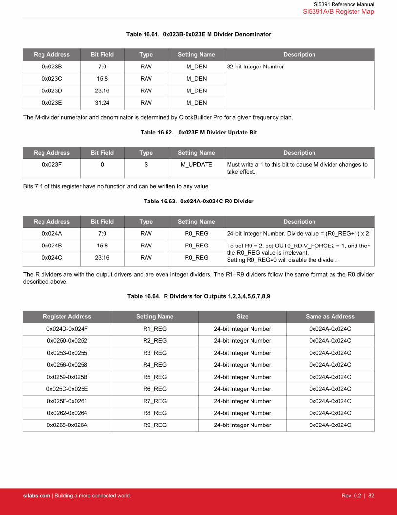
Table 16.61. 0x023B-0x023E M Divider Denominator
Reg Address Bit Field Type Setting Name Description
0x023B 7:0 R/W M_DEN 32-bit Integer Number
0x023C 15:8 R/W M_DEN
0x023D 23:16 R/W M_DEN
0x023E 31:24 R/W M_DEN
The M-divider numerator and denominator is determined by ClockBuilder Pro for a given frequency plan.
Table 16.62. 0x023F M Divider Update Bit
Reg Address Bit Field Type Setting Name Description
0x023F 0 S M_UPDATE Must write a 1 to this bit to cause M divider changes totake effect.
Bits 7:1 of this register have no function and can be written to any value.
Table 16.63. 0x024A-0x024C R0 Divider
Reg Address Bit Field Type Setting Name Description
0x024A 7:0 R/W R0_REG 24-bit Integer Number. Divide value = (R0_REG+1) x 2
To set R0 = 2, set OUT0_RDIV_FORCE2 = 1, and thenthe R0_REG value is irrelevant.Setting R0_REG=0 will disable the divider.
0x024B 15:8 R/W R0_REG
0x024C 23:16 R/W R0_REG
The R dividers are with the output drivers and are even integer dividers. The R1–R9 dividers follow the same format as the R0 dividerdescribed above.
Table 16.64. R Dividers for Outputs 1,2,3,4,5,6,7,8,9
Register Address Setting Name Size Same as Address
0x024D-0x024F R1_REG 24-bit Integer Number 0x024A-0x024C
0x0250-0x0252 R2_REG 24-bit Integer Number 0x024A-0x024C
0x0253-0x0255 R3_REG 24-bit Integer Number 0x024A-0x024C
0x0256-0x0258 R4_REG 24-bit Integer Number 0x024A-0x024C
0x0259-0x025B R5_REG 24-bit Integer Number 0x024A-0x024C
0x025C-0x025E R6_REG 24-bit Integer Number 0x024A-0x024C
0x025F-0x0261 R7_REG 24-bit Integer Number 0x024A-0x024C
0x0262-0x0264 R8_REG 24-bit Integer Number 0x024A-0x024C
0x0268-0x026A R9_REG 24-bit Integer Number 0x024A-0x024C
Si5391 Reference ManualSi5391A/B Register Map
silabs.com | Building a more connected world. Rev. 0.2 | 82
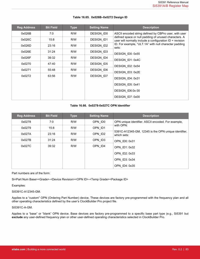
Table 16.65. 0x026B–0x0272 Design ID
Reg Address Bit Field Type Setting Name Description
0x026B 7:0 R/W DESIGN_ID0 ASCII encoded string defined by CBPro user, with userdefined space or null padding of unused characters. Auser will normally include a configuration ID + revisionID. For example, “ULT.1A” with null character paddingsets:
DESIGN_ID0: 0x55
DESIGN_ID1: 0x4C
DESIGN_ID2: 0x54
DESIGN_ID3: 0x2E
DESIGN_ID4: 0x31
DESIGN_ID5: 0x41
DESIGN_ID6:0x 00
DESIGN_ID7: 0x00
0x026C 15:8 R/W DESIGN_ID1
0x026D 23:16 R/W DESIGN_ID2
0x026E 31:24 R/W DESIGN_ID3
0x026F 39:32 R/W DESIGN_ID4
0x0270 47:40 R/W DESIGN_ID5
0x0271 55:48 R/W DESIGN_ID6
0x0272 63:56 R/W DESIGN_ID7
Table 16.66. 0x0278-0x027C OPN Identifier
Reg Address Bit Field Type Setting Name Description
0x0278 7:0 R/W OPN_ID0 OPN unique identifier. ASCII encoded. For example,with OPN:
5391C-A12345-GM, 12345 is the OPN unique identifier,which sets:
OPN_ID0: 0x31
OPN_ID1: 0x32
OPN_ID2: 0x33
OPN_ID3: 0x34
OPN_ID4: 0x35
0x0279 15:8 R/W OPN_ID1
0x027A 23:16 R/W OPN_ID2
0x027B 31:24 R/W OPN_ID3
0x027C 39:32 R/W OPN_ID4
Part numbers are of the form:
Si<Part Num Base><Grade>-<Device Revision><OPN ID>-<Temp Grade><Package ID>
Examples:
Si5391C-A12345-GM.
Applies to a “custom” OPN (Ordering Part Number) device. These devices are factory pre-programmed with the frequency plan and allother operating characteristics defined by the user’s ClockBuilder Pro project file.
Si5391C-A-GM.
Applies to a “base” or “blank” OPN device. Base devices are factory pre-programmed to a specific base part type (e.g., Si5391 butexclude any user-defined frequency plan or other user-defined operating characteristics selected in ClockBuilder Pro.
Si5391 Reference ManualSi5391A/B Register Map
silabs.com | Building a more connected world. Rev. 0.2 | 83
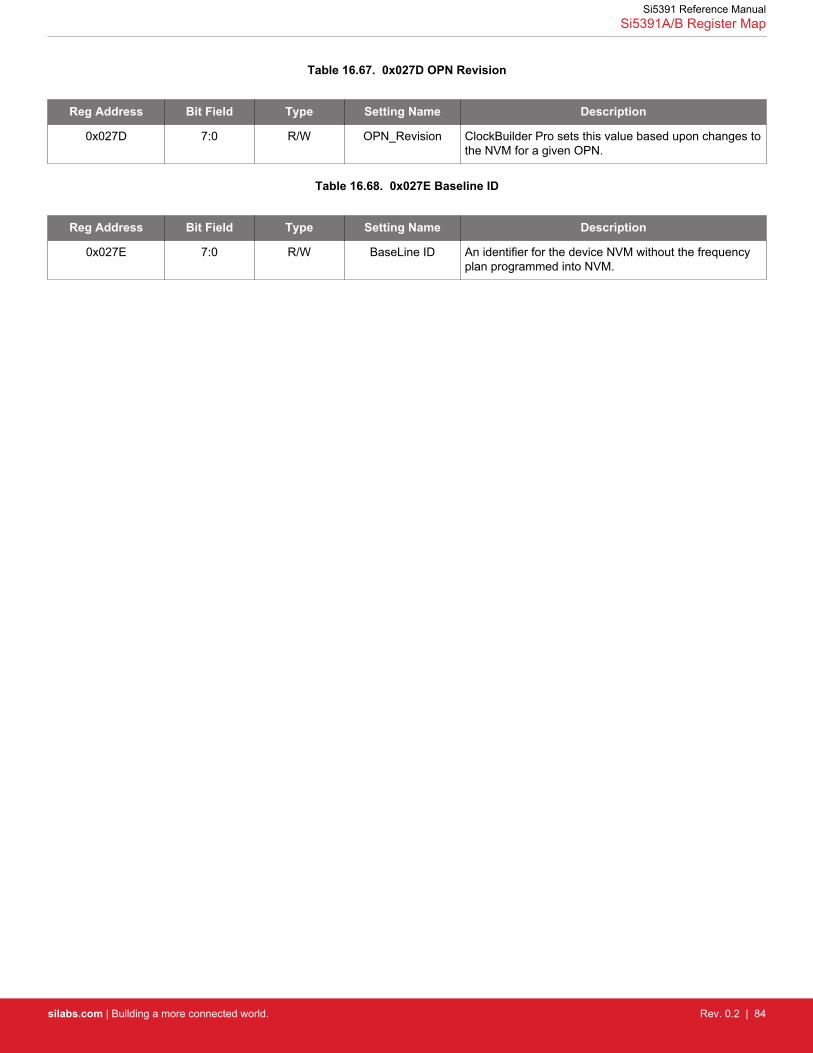
Table 16.67. 0x027D OPN Revision
Reg Address Bit Field Type Setting Name Description
0x027D 7:0 R/W OPN_Revision ClockBuilder Pro sets this value based upon changes tothe NVM for a given OPN.
Table 16.68. 0x027E Baseline ID
Reg Address Bit Field Type Setting Name Description
0x027E 7:0 R/W BaseLine ID An identifier for the device NVM without the frequencyplan programmed into NVM.
Si5391 Reference ManualSi5391A/B Register Map
silabs.com | Building a more connected world. Rev. 0.2 | 84

16.4 Page 3 Registers Si5391
Table 16.69. 0x0302–0x0307 N0 Numerator
Reg Address Bit Field Type Setting Name Description
0x0302 7:0 R/W N0_NUM 44-bit Integer Number
0x0303 15:8 R/W N0_NUM
0x0304 23:16 R/W N0_NUM
0x0305 31:24 R/W N0_NUM
0x0306 39:32 R/W N0_NUM
0x0307 43:40 R/W N0_NUM
The N dividers are interpolative dividers that are used as output dividers that feed into the R dividers. ClockBuilder Pro calculates thecorrect values for the N-dividers.
Table 16.70. 0x0308–0x030B N0 Denominator
Reg Address Bit Field Type Setting Name Description
0x0308 7:0 R/W N0_DEN 32-bit Integer Number
0x0309 15:8 R/W N0_DEN
0x030A 23:16 R/W N0_DEN
0x030B 31:24 R/W N0_DEN
Table 16.71. 0x030C N0 Divider Update Bit
Reg Address Bit Field Type Setting Name Description
0x030C 0 S N0_UPDATE Must write a 1 to this bit to cause N0 divider changes totake effect.
Table 16.72. N1, N2, N3 Numerator and Denominators
Register Address Setting Name Size Same as Address
0x030D-0x0312 N1_NUM 44-bit Integer Number 0x0302-0x0307
0x0313-0x0316 N1_DEN 32-bit Integer Number 0x0308-0x030B
0x0318-0x031D N2_NUM 44-bit Integer Number 0x0302-0x0307
0x031E-0x0321 N2_DEN 32-bit Integer Number 0x0308-0x030B
0x0323-0x0328 N3_NUM 44-bit Integer Number 0x0302-0x0307
0x0329-0x032C N3_DEN 32-bit Integer Number 0x0308-0x030B
0x032E-0x0333 N4_NUM 44-bit Integer Number 0x0302-0x0307
0x0334-0x0337 N4_DEN 32-bit Integer Number 0x0308-0x030B
Si5391 Reference ManualSi5391A/B Register Map
silabs.com | Building a more connected world. Rev. 0.2 | 85

Table 16.73. 0x0317 N1 Divider Update Bit
Reg Address Bit Field Type Setting Name Description
0x0317 0 S N1_UPDATE Must write a 1 to this bit to cause N1 divider changes totake effect.
Table 16.74. 0x0322 N2 Divider Update Bit
Reg Address Bit Field Type Setting Name Description
0x0322 0 S N2_UPDATE Must write a 1 to this bit to cause N2 divider changes totake effect.
Table 16.75. 0x032D N3 Divider Update Bit
Reg Address Bit Field Type Setting Name Description
0x032D 0 S N3_UPDATE Must write a 1 to this bit to cause N3 divider changes totake effect.
Table 16.76. 0x0338 N4 Divider Update Bit
Reg Address Bit Field Type Setting Name Description
0x0338 0 S N4_UPDATE Must write a 1 to this bit to cause N4 divider changes totake effect.
Table 16.77. 0x0338 All N Dividers Update Bit
Reg Address Bit Field Type Setting Name Description
0x0338 1 S N_UPDATE Writing a 1 to this bit will update all N dividers to the lat-est value written to them. A specific N divider that hasnot been changed will not be affected by writing a 1 tothis bit. When this bit is written to a 1, all other bits inthis byte should only be written to a 0.
Table 16.78. 0x0339 FINC/FDEC Masks
Reg Address Bit Field Type Setting Name Description
0x0339 4:0 R/W N_FSTEP_MSK 0 to enable FINC/FDEC updates
1 to disable FINC/FDEC updates
• Bit 0 corresponds to MultiSynth N0 N_FSTEP_MSK 0x0339[0]• Bit 1 corresponds to MultiSynth N1 N_FSTEP_MSK 0x0339[1]• Bit 2 corresponds to MultiSynth N2 N_FSTEP_MSK 0x0339[2]• Bit 3 corresponds to MultiSynth N3 N_FSTEP_MSK 0x0339[3]• Bit 4 corresponds to MultiSynth N4 N_FSTEP_MSK 0x0339[4]
There is one mask bit for each of the five N dividers.
Si5391 Reference ManualSi5391A/B Register Map
silabs.com | Building a more connected world. Rev. 0.2 | 86
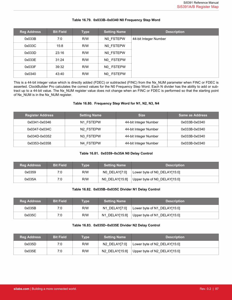
Table 16.79. 0x033B–0x0340 N0 Frequency Step Word
Reg Address Bit Field Type Setting Name Description
0x033B 7:0 R/W N0_FSTEPW 44-bit Integer Number
0x033C 15:8 R/W N0_FSTEPW
0x033D 23:16 R/W N0_FSTEPW
0x033E 31:24 R/W N0_ FSTEPW
0x033F 39:32 R/W N0_ FSTEPW
0x0340 43:40 R/W N0_ FSTEPW
This is a 44-bit integer value which is directly added (FDEC) or subtracted (FINC) from the Nx_NUM parameter when FINC or FDEC isasserted. ClockBuilder Pro calculates the correct values for the N0 Frequency Step Word. Each N divider has the ability to add or sub-tract up to a 44-bit value. The Nx_NUM register value does not change when an FINC or FDEC is performed so that the starting pointof Nx_NUM is in the Nx_NUM register.
Table 16.80. Frequency Step Word for N1, N2, N3, N4
Register Address Setting Name Size Same as Address
0x0341-0x0346 N1_FSTEPW 44-bit Integer Number 0x033B-0x0340
0x0347-0x034C N2_FSTEPW 44-bit Integer Number 0x033B-0x0340
0x034D-0x0352 N3_FSTEPW 44-bit Integer Number 0x033B-0x0340
0x0353-0x0358 N4_FSTEPW 44-bit Integer Number 0x033B-0x0340
Table 16.81. 0x0359–0x35A N0 Delay Control
Reg Address Bit Field Type Setting Name Description
0x0359 7:0 R/W N0_DELAY[7:0] Lower byte of N0_DELAY[15:0]
0x035A 7:0 R/W N0_DELAY[15:8] Upper byte of N0_DELAY[15:0]
Table 16.82. 0x035B–0x035C Divider N1 Delay Control
Reg Address Bit Field Type Setting Name Description
0x035B 7:0 R/W N1_DELAY[7:0] Lower byte of N1_DELAY[15:0]
0x035C 7:0 R/W N1_DELAY[15:8] Upper byte of N1_DELAY[15:0]
Table 16.83. 0x035D–0x035E Divider N2 Delay Control
Reg Address Bit Field Type Setting Name Description
0x035D 7:0 R/W N2_DELAY[7:0] Lower byte of N2_DELAY[15:0]
0x035E 7:0 R/W N2_DELAY[15:8] Upper byte of N2_DELAY[15:0]
Si5391 Reference ManualSi5391A/B Register Map
silabs.com | Building a more connected world. Rev. 0.2 | 87

Table 16.84. 0x035F–0x0360 Divider N3 Delay Control
Reg Address Bit Field Type Setting Name Description
0x035F 7:0 R/W N3_DELAY[7:0] Lower byte of N3_DELAY[15:0]
0x0360 7:0 R/W N3_DELAY[15:8] Upper byte of N3_DELAY[15:0]
Table 16.85. 0x0361–0x0362 Divider N4 Delay Control
Reg Address Bit Field Type Setting Name Description
0x0361 7:0 R/W N4_DELAY[7:0] Lower byte of N4_DELAY[15:0]
0x0362 15:8 R/W N4_DELAY[15:8] Upper byte of N4_DELAY[15:0]
The delay in seconds is Nx_DELAY/(256 x Fvco) where Fvco is the VCO frequency in Hz. The maximum positive and negative delay is±(215 – 1) / (256 x Fvco). Nx_DELAY values are only applied at power up or during a reset. ClockBuilder Pro calculates the correctvalue for this register. It is expected that only the upper byte of Nx_DELAY is necessary as the step sizes in the lower byte are so smallas to be essentially irrelevant. At power up or when the RSTb pin is asserted, the Nx_DELAY values are downloaded from NVM. IfNx_DELAY is written via the serial port, the SOFT_RST reset bit must be written to cause the delay to take effect.
Si5391 Reference ManualSi5391A/B Register Map
silabs.com | Building a more connected world. Rev. 0.2 | 88

16.5 Page 9 Registers Si5391
Table 16.86. 0x090E XAXB Configuration
Reg Address Bit Field Type Setting Name Description
0x090E 0 R/W XAXB_EXTCLK_EN 0 to use a crystal at the XAXB pins
1 to use an external clock source at the XAXB pins. Asingled ended clock must be applied at the XA input.
0x090E 1 R/W XAXB_PDNB 0-Power down the oscillator and buffer circuitry at theXA/XB pins
1- No power down
Table 16.87. 0x091C Enable Zero Delay Mode
Reg Address Bit Field Type Setting Name Description
0x091C 2:0 R/W ZDM_EN 3 = Zero delay mode.
4 = Normal mode.
All other values must not be written.
Table 16.88. 0x0943 Status and Control I/O Voltage Select
Reg Address Bit Field Type Setting Name Description
0x0943 0 R/W IO_VDD_SEL 0 for 1.8 V external connections
1 for 3.3 V external connections
The IO_VDD_SEL configuration bit selects the option of operating the serial interface voltage thresholds from the VDD or the VDDApin. By default the IO_VDD_SEL bit is set to the VDD option. The serial interface pins are always 3.3 V tolerant even when the device'sVDD pin is supplied from a 1.8 V source. When the I2C or SPI host is operating at 3.3 V and the Si5391 IO_VDD_SEL = 1.8 V, the hostshould write the IO_VDD_SEL configuration bit to the VDDA option. This will ensure that both the host and the serial interface areoperating at the optimum voltage thresholds. The IO_VDD_SEL bit also affects the status pin levels and control pin thresholds. WhenIO_VDD_SEL = 0, the status outputs will have a VOH of ~1.8 V. When IO_VDD_SEL = 1 the status outputs will have a VOH of ~3.3 V.When IO_VDD_SEL=0, the control input pins will have an input threshold based upon the VDD supply voltage of 1.8 V. WhenIO_VDD_SEL=1, the control input pins will have an input threshold based upon the VDDA supply voltage of 3.3 V. See Table 4 andTable 6 of the Si5391 data sheet for details.
Table 16.89. 0x0949 Clock Input Control
Reg Address Bit Field Type Setting Name Description
0x0949 3:0 R/W IN_EN Enables for the four inputs clocks, IN0 through FB_IN.
1 to enable, 0 to disable
• Input 0 corresponds to IN_EN 0x0949 [0].• Input 1 corresponds to IN_EN 0x0949 [1].• Input 2 corresponds to IN_EN 0x0949 [2].• FB_IN corresponds to IN_EN 0x0949 [3].
Si5391 Reference ManualSi5391A/B Register Map
silabs.com | Building a more connected world. Rev. 0.2 | 89

Table 16.90. 0x094A Input Clock Routing Enable
Reg Address Bit Field Type Setting Name Description
0x094A 6:4 R/W INx_TO_PFD_EN When = 1, enables the routing of the 3 input clocksIN0,1,2 to the Phase Detector. Each bit corresponds tothe inputs as follows [6:4] = [IN2 IN1 IN0]. IN_SEL isused to select the input clock that is applied to thephase detector.
Table 16.91. 0x095E
Reg Address Bit Field Type Setting Name Description
0x095E 0 R/W M_INTEGER
16.6 Page A Registers Si5391
Table 16.92. 0x0A03 N Divider Clocks
Reg Address Bit Field Type Setting Name Description
0x0A03 4:0 R/W N_CLK_TO_OUTX_EN
BIts in this field correspond to the N dividers as [N4 N3N2 N1 N0]. If an N divider is used, the corresponding bitmust be 1. See also registers 0x0A05 and 0x0B4A[4:0].
Table 16.93. 0x0A04 N Divider Phase Interpolator Bypass
Reg Address Bit Field Type Setting Name Description
0x0A04 4:0 R/W N_PIBYP Bypasses the Phase Interpolator of the N Multisynth di-vider. Set to a 1 when the value of N divider is integerand will not be used as a DCO. Set to a 0 when the val-ue of N is fractional (used as a DCO). Slightly lower out-put jitter may occur when the Phase Interpolator is by-passed (=1). Bits in this field correspond to the N divid-ers as [N4 N3 N2 N1 N0].
Table 16.94. 0x0A05 N Divider Power Down
Reg Address Bit Field Type Setting Name Description
0x0A05 4:0 R/W N_PDNB Powers down the N divider. If an N divider is not used,set the respective bit to 0 to power it down. Bits in thisfield correspond to the N dividers as [N4 N3 N2 N1 N0].See also registers 0x0A03 and 0x0B4A[4;0].
16.7 Page B Registers Si5391
Table 16.95. 0x0B44 Loss of Signal Clock Disable
Reg Address Bit Field Type Setting Name Description
0x0B44 3:0 R/W PDIV_ENB
Si5391 Reference ManualSi5391A/B Register Map
silabs.com | Building a more connected world. Rev. 0.2 | 90
Table 16.96. 0x0B4A Divider Clock Disables
Reg Address Bit Field Type Setting Name Description
0x0B4A 4:0 R/W N_CLK_DIS Controls the clock to the N divider. If an N divider isused the corresponding bit must be 0. [N3 N2 N1 N0].See also registers 0x0A03 and 0x0A05.
Table 16.97. 0x0B57
Reg Address Bit Field Type Name Description
0x0B57 7:0 R/W VCO_RESET_CAL-CODE
12-bit value
0x0B58 11:8 R/W VCO_RESET_CAL-CODE
Si5391 Reference ManualSi5391A/B Register Map
silabs.com | Building a more connected world. Rev. 0.2 | 91
17. Revision History
Revision 0.2
July 2018• Updated Section 2.1 Grade P Restrictions and Requirements
Revision 0.1
June 2018• Initial Release
Si5391 Reference ManualRevision History
silabs.com | Building a more connected world. Rev. 0.2 | 92

http://www.silabs.com
Silicon Laboratories Inc.400 West Cesar ChavezAustin, TX 78701USA
Smart. Connected. Energy-Friendly.
Productswww.silabs.com/products
Qualitywww.silabs.com/quality
Support and Communitycommunity.silabs.com
DisclaimerSilicon Labs intends to provide customers with the latest, accurate, and in-depth documentation of all peripherals and modules available for system and software implementers using or intending to use the Silicon Labs products. Characterization data, available modules and peripherals, memory sizes and memory addresses refer to each specific device, and "Typical" parameters provided can and do vary in different applications. Application examples described herein are for illustrative purposes only. Silicon Labs reserves the right to make changes without further notice and limitation to product information, specifications, and descriptions herein, and does not give warranties as to the accuracy or completeness of the included information. Silicon Labs shall have no liability for the consequences of use of the information supplied herein. This document does not imply or express copyright licenses granted hereunder to design or fabricate any integrated circuits. The products are not designed or authorized to be used within any Life Support System without the specific written consent of Silicon Labs. A "Life Support System" is any product or system intended to support or sustain life and/or health, which, if it fails, can be reasonably expected to result in significant personal injury or death. Silicon Labs products are not designed or authorized for military applications. Silicon Labs products shall under no circumstances be used in weapons of mass destruction including (but not limited to) nuclear, biological or chemical weapons, or missiles capable of delivering such weapons.
Trademark InformationSilicon Laboratories Inc.® , Silicon Laboratories®, Silicon Labs®, SiLabs® and the Silicon Labs logo®, Bluegiga®, Bluegiga Logo®, Clockbuilder®, CMEMS®, DSPLL®, EFM®, EFM32®, EFR, Ember®, Energy Micro, Energy Micro logo and combinations thereof, "the world’s most energy friendly microcontrollers", Ember®, EZLink®, EZRadio®, EZRadioPRO®, Gecko®, ISOmodem®, Micrium, Precision32®, ProSLIC®, Simplicity Studio®, SiPHY®, Telegesis, the Telegesis Logo®, USBXpress®, Zentri, Z-Wave and others are trademarks or registered trademarks of Silicon Labs. ARM, CORTEX, Cortex-M3 and THUMB are trademarks or registered trademarks of ARM Holdings. Keil is a registered trademark of ARM Limited. All other products or brand names mentioned herein are trademarks of their respective holders.