si5395/94/92 data sheet...si5395/94/92 data sheet 12-channel, any-frequency, any-output jitter...
TRANSCRIPT

Si5395/94/92 Data Sheet
12-Channel, Any-Frequency, Any-Output Jitter Attenuator/Clock Multiplier with Ultra-Low JitterThe Si5395/94/92 Jitter attenuators combine fourth-generation DSPLL™ and Multi-Synth™ technologies to deliver ultra-low jitter (69 fs) for high performance applica-tions like 56G SerDes. They are used in applications that demand the highest levelof integration and jitter performance. All PLL components are integrated on-chip,eliminating the risk of noise coupling associated with discrete solutions. Devicegrades J/K/L/M/E have an integrated reference to save board space, improve sys-tem reliability and reduces the effect of acoustic emissions noise caused by temper-ature ramps. Grades A/B/C/D/P use an external crystal (XTAL) or crystal oscillator(XO) reference.
The Si5395/94/92 support free-run, synchronous and holdover modes as well as en-hanced hitless switching, minimizing the phase transients associated when switchingbetween input clocks. These devices are programmable via a serial interface with in-circuit programmable non-volatile memory (NVM) so they always power up with aknown frequency configuration. Programming the Si5395/94/92 is easy with SiliconLabs’ ClockBuilderTM Pro software. Factory preprogrammed devices are also availa-ble.
For more information, visit the https://www.silabs.com/contact-sales page.
Applications:• 56G/112G PAM4 SerDes clocking• OTN muxponders and transponders• 10/40/100/200/400G networking line cards• 10/40/100/400 GbE Synchronous Ethernet (ITU-T G.8262)• Medical imaging• Test and measurement
KEY FEATURES
• Generates any combination of outputfrequencies from any input frequency
• Ultra low phase jitter:• 69 fs RMS (Grade P)• 71 fs RMS (Grade E)• 85 fs RMS (integer mode)• 100 fs RMS (fractional mode)
• Enhanced hitless switching minimizes outputphase transients (0.2 ns typ)
• Input frequency range• Differential: 8 kHz to 750 MHz• LVCMOS: 8 kHz to 250 MHz
• Output frequency range• Differential: 100 Hz to 1028 MHz• LVCMOS: 100 Hz to 250 MHz
• Meets G.8262, E.8262.1 EEC Standards• Status monitoring• Si5395: 4 input, 12 output• Si5394: 4 input, 4 output• Si5392: 4 input, 2 output• External reference: Grades A/B/C/D/P• Integrated reference: Grades J/K/L/M/E• Drop-in compatible with Si5345/44/42
Up to 12 Output Clocks
Si5394Si5395
Control NVM
Status Flags Status Monitor
Integrated Reference* MultiSynth
MultiSynth
MultiSynth
MultiSynth
MultiSynth
DSPLL
Si5392
4 InputClocks
IN0
IN1
IN2
IN3/FB_IN
OUT7
OUT6
OUT5
OUT1
OUT4
OUT3
OUT2
OUT0÷INT
÷INT
÷INT
÷INT
÷INT
÷INT
÷INT
÷INT
OUT9
OUT8
÷INT
÷INT
÷FRAC
÷FRAC
÷FRAC
÷FRAC
*Only for Si539x J/K/L/M/E grades. Si539x A/B/C/D/P grades have external reference (XTAL or XO)
I2C/SPI OUT9A÷INT
OUT0A÷INT
silabs.com | Building a more connected world. Rev. 1.1
1. Features List
The Si5395/94/92 features are listed below:• Generates any output frequency in any format from any input
frequency• External XTAL or XO reference (A/B/C/D/P)• Integrated reference (J/K/L/M/E)• Ultra-low phase jitter of 69 fs (P-Grade)• Dynamic phase adjust• Input frequency range
• Differential: 8 kHz–750 MHz• LVCMOS: 8 kHz–250 MHz
• Output frequency range• Differential: 100 Hz to 1028 MHz• LVCMOS: 100 Hz to 250 MHz
• Programmable jitter attenuation bandwidth: 0.1 Hz to 4 kHz• Meets requirements of:
• ITU-T G.8262 (SyncE) EEC Options 1 and 2• ITU-T G.8262.1 (Enhanced SyncE) eEEC
• Highly configurable outputs compatible with LVDS, LVPECL,LVCMOS, CML, and HCSL with programmable signal ampli-tude
• Status monitoring (LOS, OOF, LOL)• Enhanced hitless switching for 8 kHz, 19.44 MHz, 25 MHz in-
puts and other frequencies• Locks to gapped clock inputs• Free-run and holdover modes• Drop-in compatible with Si5345/44/42
• Optional zero delay mode• Fast-lock acquisition for low nominal bandwidths• Independent Frequency-on-the fly for each MultiSynth• DCO mode: as low as 0.001 ppb step size• Core voltage
• VDD: 1.8 V ±5%• VDDA: 3.3 V ±5%
• Independent output clock supply pins• 3.3 V, 2.5 V, or 1.8 V
• Serial interface: I2C or SPI• In-circuit programmable with non-volatile OTP memory• ClockBuilder Pro software simplifies device configuration• Si5395: 4 input, 12 output
• Grade A/B/C/D/P: 64-QFN 9×9 mm• Grade J/K/L/M/E: 64-LGA 9x9 mm
• Si5394: 4 input, 4 output• Grade A/B/C/D/P: 44-QFN 7×7 mm• Grade J/K/L/M/E: 44-LGA 7x7 mm
• Si5392: 4 input, 2 output• Grade A/B/C/D/P: 44-QFN 7×7 mm• Grade J/K/L/M/E: 44-LGA 7x7 mm
• Temperature range: –40 to +85 °C• Pb-free, RoHS-6 compliant
Si5395/94/92 Data SheetFeatures List
silabs.com | Building a more connected world. Rev. 1.1 | 2

2. Related Documents
Table 2.1. Related Documentation and Software
Document/Resource Description/URL
Si5395/94/92 Family Reference Manual Si5395-94-92 Family Reference Manual
Crystal Reference Manual (Grades A/B/C/D/P only) https://www.silabs.com/documents/public/reference-manuals/si534x-8x-9x-recommended-crystals-rm.pdf
UG387: Si5392 Evaluation Board User's Guide https://www.silabs.com/documents/public/user-guides/ug387-si5392-evb.pdf
UG334: Si5394 Evaluation Board User's Guide https://www.silabs.com/documents/public/user-guides/ug334-si5394evb.pdf
UG335: Si5395 Evaluation Board User's Guide https://www.silabs.com/documents/public/user-guides/ug335-si5395evb.pdf
AN1151: Using the Si539x in 56G SerDes Applications https://www.silabs.com/documents/public/application-notes/an1151-using-si539x.pdf
AN1155: Differences between Si5342-47 and Si5392-97 https://www.silabs.com/documents/public/application-notes/an1155-differences-between-si5342-47-and-si5392-97.pdf
AN1178: Frequency-On-the-Fly for Silicon Labs Jitter Attenuatorsand Clock Generators
https://www.silabs.com/documents/public/application-notes/an1178-frequency-otf-jitter-atten-clock-gen.pdf
Frequently Asked Questions http://www.silabs.com/Si5395-94-92-FAQ
Quality and Reliability http://www.silabs.com/quality
Development Kits https://www.silabs.com/products/development-tools/timing/clock#highperformance
ClockBuilder Pro (CBPro) Software https://www.silabs.com/products/development-tools/software/clockbuilder-pro-software
Si5395/94/92 Data SheetRelated Documents
silabs.com | Building a more connected world. Rev. 1.1 | 3

3. Ordering Guide
Table 3.1. Si5395/94/92 A/B/C/D/P Ordering Guide (External Reference)
Ordering PartNumber (OPN)
Number of Input/Output Clocks
Output ClockFrequency Range (MHz)
Supported FrequencySynthesis Modes Package Reference
Si5395
Si5395A-A-GM1, 2
4/12
0.0001 to 1028 MHzInteger and Fractional
64-QFN9×9 mm External
Si5395B-A-GM1, 2 0.0001 to 350 MHz
Si5395C-A-GM1, 2 0.0001 to 1028 MHzInteger Only
Si5395D-A-GM1, 2 0.0001 to 350 MHz
Si5395P-A-GM1, 2 Up to 3 domains(Section 4.9.2 Grades P and E) Precision Calibration
Si5394
Si5394A-A-GM1, 2
4/4
0.0001 to 1028 MHzInteger and Fractional
44-QFN7×7 mm External
Si5394B-A-GM1, 2 0.0001 to 350 MHz
Si5394C-A-GM1, 2 0.0001 to 1028 MHzInteger Only
Si5394D-A-GM1, 2 0.0001 to 350 MHz
Si5394P-A-GM1, 2 Up to 2 domains(Section 4.9.2 Grades P and E) Precision Calibration
Si5392
Si5392A-A-GM1, 2
4/2
0.0001 to 1028 MHzInteger and Fractional
44-QFN7×7 mm External
Si5392B-A-GM1, 2 0.0001 to 350 MHz
Si5392C-A-GM1, 2 0.0001 to 1028 MHzInteger Only
Si5392D-A-GM1, 2 0.0001to 350 MHz
Si5392P-A-GM1, 2 1 domain(Section 4.9.2 Grades P and E) Precision Calibration
Si5395/94/92 Evaluation Board
Si5395A-A-EVB 12-output Any-frequency, any Output — 64-QFNEVB —
Si5395P-A-EVB 12-output Low jitter clocks for 56G PAM4SerDes — 64-QFN
EVB —
Si5394A-A-EVB 4-output Any-frequency, any Output — 44-QFNEVB —
Si5394P-A-EVB 4-output Low jitter clocks for 56G PAM4SerDes — 44-QFN
EVB —
Notes:1. Add an R at the end of the OPN to denote tape and reel ordering options.2. Custom, factory preprogrammed devices are available. Ordering part numbers are assigned by Silicon Labs and the ClockBuilder
Pro software utility. Custom part number format is “Si5395A-Axxxxx-GM” where “xxxxx” is a unique numerical sequence repre-senting the preprogrammed configuration.
Si5395/94/92 Data SheetOrdering Guide
silabs.com | Building a more connected world. Rev. 1.1 | 4

Table 3.2. Si5395/4/2 J/K/L/M/E Ordering guide (Integrated Reference)
Ordering PartNumber (OPN)
Number of Input/Output Clocks
Output ClockFrequency Range (MHz)
Supported FrequencySynthesis Modes Package Reference
Si5395
Si5395J-A-GM1, 2
4/12
0.0001 to 1028 MHzInteger and Fractional
64-LGA9×9 mm Internal
Si5395K-A-GM1, 2 0.0001 to 350 MHz
Si5395L-A-GM1, 2 0.0001 to 1028 MHzInteger Only
Si5395M-A-GM1, 2 0.0001 to 350 MHz
Si5395E-A-GM1, 2 Up to 3 domains(Section 4.9.2 Grades P and E) Precision Calibration
Si5394
Si5394J-A-GM1, 2
4/4
0.0001 to 1028 MHzInteger and Fractional
44-LGA7×7 mm Internal
Si5394K-A-GM1, 2 0.0001 to 350 MHz
Si5394L-A-GM1, 2 0.0001 to 1028 MHzInteger Only
Si5394M-A-GM1, 2 0.0001 to 350 MHz
Si5394E-A-GM1, 2 Up to 2 domains(Section 4.9.2 Grades P and E) Precision Calibration
Si5392
Si5392J-A-GM1, 2
4/2
0.0001 to 1028 MHzInteger and Fractional
44-LGA7×7 mm Internal
Si5392K-A-GM1, 2 0.0001 to 350 MHz
Si5392L-A-GM1, 2 0.0001 to 1028 MHzInteger Only
Si5392M-A-GM1, 2 0.0001to 350 MHz
Si5392E-A-GM1, 2 1 domain(Section 4.9.2 Grades P and E) Precision Calibration
Si5395/94/92 Evaluation Board
Si5395J-A-EVB 12-output Any-frequency, any Output — 64-LGAEVB —
Si5395E-A-EVB 12-output Low jitter clocks for 56G PAM4SerDes — 64-LGA
EVB —
Si5394J-A-EVB 4-output Any-frequency, any Output — 44-LGAEVB —
Si5394E-A-EVB 4-output Low jitter clocks for 56G PAM4SerDes — 44-LGA
EVB —
Si5392J-A-EVB 2-output Any-frequency, any Output — 44-LGAEVB —
Si5392E-A-EVB 2-output Low jitter clocks for 56G PAM4SerDes — 44-LGA
EVB —
Si5395/94/92 Data SheetOrdering Guide
silabs.com | Building a more connected world. Rev. 1.1 | 5

Ordering PartNumber (OPN)
Number of Input/Output Clocks
Output ClockFrequency Range (MHz)
Supported FrequencySynthesis Modes Package Reference
Notes:1. Add an R at the end of the OPN to denote tape and reel ordering options.2. Custom, factory preprogrammed devices are available. Ordering part numbers are assigned by Silicon Labs and the ClockBuilder
Pro software utility. Custom part number format is “Si5395J-Axxxxx-GM” where “xxxxx” is a unique numerical sequence repre-senting the preprogrammed configuration.
Figure 3.1. Ordering Part Number Fields
Si5395/94/92 Data SheetOrdering Guide
silabs.com | Building a more connected world. Rev. 1.1 | 6
Table of Contents1. Features List . . . . . . . . . . . . . . . . . . . . . . . . . . . . . . . 2
2. Related Documents . . . . . . . . . . . . . . . . . . . . . . . . . . . . . 3
3. Ordering Guide . . . . . . . . . . . . . . . . . . . . . . . . . . . . . . 4
4. Functional Description. . . . . . . . . . . . . . . . . . . . . . . . . . . . 94.1 Frequency Configuration . . . . . . . . . . . . . . . . . . . . . . . . . . 9
4.2 DSPLL Loop Bandwidth . . . . . . . . . . . . . . . . . . . . . . . . . . . 9
4.3 Fastlock Feature . . . . . . . . . . . . . . . . . . . . . . . . . . . . . 9
4.4 Modes of Operation . . . . . . . . . . . . . . . . . . . . . . . . . . . . 94.4.1 Initialization and Reset . . . . . . . . . . . . . . . . . . . . . . . . . .104.4.2 Freerun Mode . . . . . . . . . . . . . . . . . . . . . . . . . . . . .104.4.3 Lock Acquisition Mode . . . . . . . . . . . . . . . . . . . . . . . . . .104.4.4 Locked Mode . . . . . . . . . . . . . . . . . . . . . . . . . . . . .104.4.5 Holdover Mode . . . . . . . . . . . . . . . . . . . . . . . . . . . .114.4.6 Frequency-on-the-Fly (FOTF) . . . . . . . . . . . . . . . . . . . . . . .11
4.5 Digitally Controlled Oscillator (DCO) Mode (Grade A/B/C/D and J/K/L/M ) . . . . . . . . . .11
4.6 External Reference (Grade A/B/C/D/P Only) . . . . . . . . . . . . . . . . . . . .12
4.7 Inputs (IN0, IN1, IN2, IN3) . . . . . . . . . . . . . . . . . . . . . . . . . .124.7.1 Manual Input Selection (IN0, IN1, IN2, IN3) . . . . . . . . . . . . . . . . . . .134.7.2 Automatic Input Selection (IN0, IN1, IN2, IN3) . . . . . . . . . . . . . . . . . .134.7.3 Hitless Input Switching . . . . . . . . . . . . . . . . . . . . . . . . . .144.7.4 Frequency Ramped Input Switching . . . . . . . . . . . . . . . . . . . . .154.7.5 Glitchless Input Switching . . . . . . . . . . . . . . . . . . . . . . . . .154.7.6 Synchronizing to Gapped Input Clocks (Grade A/B/C/D and J/K/L/M Only) . . . . . . . .16
4.8 Fault Monitoring . . . . . . . . . . . . . . . . . . . . . . . . . . . . .164.8.1 Input LOS Detection. . . . . . . . . . . . . . . . . . . . . . . . . . .174.8.2 XA/XB LOS Detection . . . . . . . . . . . . . . . . . . . . . . . . . .174.8.3 OOF Detection . . . . . . . . . . . . . . . . . . . . . . . . . . . .174.8.4 LOL Detection. . . . . . . . . . . . . . . . . . . . . . . . . . . . .184.8.5 Interrupt Pin (INTRb) . . . . . . . . . . . . . . . . . . . . . . . . . .19
4.9 Outputs . . . . . . . . . . . . . . . . . . . . . . . . . . . . . . . .194.9.1 Grade A/B/C/D and J/K/L/M . . . . . . . . . . . . . . . . . . . . . . . .194.9.2 Grades P and E . . . . . . . . . . . . . . . . . . . . . . . . . . . .204.9.3 Output Crosspoint . . . . . . . . . . . . . . . . . . . . . . . . . . .214.9.4 Output Signal Format . . . . . . . . . . . . . . . . . . . . . . . . . .214.9.5 Programmable Common Mode Voltage For Differential Outputs . . . . . . . . . . . .214.9.6 LVCMOS Output Impedance Selection . . . . . . . . . . . . . . . . . . . .214.9.7 LVCMOS Output Signal Swing . . . . . . . . . . . . . . . . . . . . . . .214.9.8 LVCMOS Output Polarity . . . . . . . . . . . . . . . . . . . . . . . . .214.9.9 Output Enable/Disable . . . . . . . . . . . . . . . . . . . . . . . . . .214.9.10 Output Driver State When Disabled . . . . . . . . . . . . . . . . . . . . .224.9.11 Synchronous Output Disable Feature . . . . . . . . . . . . . . . . . . . .224.9.12 Input/Output Skew Control . . . . . . . . . . . . . . . . . . . . . . . .22
silabs.com | Building a more connected world. Rev. 1.1 | 7

4.9.13 Zero Delay Mode . . . . . . . . . . . . . . . . . . . . . . . . . . .224.9.14 Output Divider (R) Synchronization . . . . . . . . . . . . . . . . . . . . .23
4.10 Power Management . . . . . . . . . . . . . . . . . . . . . . . . . . . .23
4.11 In-Circuit Programming. . . . . . . . . . . . . . . . . . . . . . . . . . .23
4.12 Serial Interface . . . . . . . . . . . . . . . . . . . . . . . . . . . . .23
4.13 Custom Factory Preprogrammed Parts . . . . . . . . . . . . . . . . . . . . .23
4.14 Register Map . . . . . . . . . . . . . . . . . . . . . . . . . . . . . .23
5. Electrical Specifications . . . . . . . . . . . . . . . . . . . . . . . . . . 24
6. Typical Application Schematic . . . . . . . . . . . . . . . . . . . . . . . . 42
7. Detailed Block Diagrams . . . . . . . . . . . . . . . . . . . . . . . . . . 43
8. Typical Operating Characteristics . . . . . . . . . . . . . . . . . . . . . .44
9. Pin Descriptions . . . . . . . . . . . . . . . . . . . . . . . . . . . . . 46
10. Package Outlines . . . . . . . . . . . . . . . . . . . . . . . . . . . . 5210.1 Si5395 A/B/C/D/P (External Reference) 9x9 mm 64-QFN Package Diagram . . . . . . . . .52
10.2 Si5395 J/K/L/M/E (Internal Reference) 9x9 mm 64-LGA Package Diagram . . . . . . . . .53
10.3 Si5394 and Si5392 A/B/C/D/P (External Reference) 7x7 mm 44-QFN Package Diagram . . . .54
10.4 Si5394 and Si5392 J/K/L/M/E (Internal Reference) 7x7 mm 44-LGA Package Diagram . . . . .55
11. PCB Land Pattern . . . . . . . . . . . . . . . . . . . . . . . . . . . . 56
12. Top Marking . . . . . . . . . . . . . . . . . . . . . . . . . . . . . . 58
13. Revision History. . . . . . . . . . . . . . . . . . . . . . . . . . . . . 59
silabs.com | Building a more connected world. Rev. 1.1 | 8

4. Functional Description
The Si5392-95’s internal DSPLL provides jitter attenuation and any-frequency multiplication of the selected input frequency. Fractionalinput dividers (P) allow the DSPLL to perform hitless switching between input clocks (INx) that are fractionally related. Input switching iscontrolled manually or automatically using an internal state machine. The oscillator circuit (OSC) provides a frequency reference whichdetermines output frequency stability and accuracy while the device is in free-run or holdover mode. The high-performance MultiSynthdividers (N) generate integer or fractionally related output frequencies for the output stage. A crosspoint switch connects any of theMultiSynth generated frequencies to any of the outputs. Additional integer division (R) determines the final output frequency.
4.1 Frequency Configuration
The frequency configuration of the DSPLL is programmable through the serial interface and can also be stored in non-volatile memory.The combination of fractional input dividers (Pn/Pd), fractional frequency multiplication (Mn/Md), fractional output MultiSynth division(Nn/Nd), and integer output division (Rn) allows the generation of virtually any output frequency on any of the outputs. All divider valuesfor a specific frequency plan are easily determined using the ClockBuilder Pro utility.
4.2 DSPLL Loop Bandwidth
The DSPLL loop bandwidth determines the amount of input clock jitter attenuation. Register configurable DSPLL loop bandwidth set-tings in the range of 0.1 Hz to 4 kHz are available for selection for Grade A/B/C/D. Since the loop bandwidth is controlled digitally, theDSPLL will always remain stable with less than 0.1 dB of peaking regardless of the loop bandwidth selection. For grade P and E devi-ces, the DSPLL bandwidth is fixed at 100 Hz.
4.3 Fastlock Feature
Selecting a low DSPLL loop bandwidth (e.g. 0.1 Hz) will generally lengthen the lock acquisition time. The fastlock feature allows settinga temporary Fastlock Loop Bandwidth that is used during the lock acquisition process. Higher fastlock loop bandwidth settings will ena-ble the DSPLLs to lock faster. Fastlock Loop Bandwidth settings of in the range of 100 Hz to 4 kHz are available for selection. TheDSPLL will revert to its normal loop bandwidth once lock acquisition has completed.
4.4 Modes of Operation
Once initialization is complete the DSPLL operates in one of four modes: Free-run Mode, Lock Acquisition Mode, Locked Mode, orHoldover Mode. A state diagram showing the modes of operation is shown in the figure below. The following sections describe each ofthese modes in greater detail.
No valid input clocks
selected
Lock Acquisition (Fast Lock)
Locked Mode
Holdover Mode
Phase lock on selected input
clock is achieved
An input is qualified and available for
selection
No valid input clocks available
for selection
Free-run
Valid input clock selected
Reset and Initialization
Power-Up
Selected input clock fails
Yes
No
Holdover History Valid?
Other Valid Clock Inputs Available?No
Yes
Input Clock Switch
Figure 4.1. Modes of Operation
Si5395/94/92 Data SheetFunctional Description
silabs.com | Building a more connected world. Rev. 1.1 | 9

4.4.1 Initialization and Reset
Once power is applied, the device begins an initialization period, downloads default register values and configuration data from NVM,and performs other initialization tasks. To communicate with the device through the serial interface, wait untl the initialization period iscomplete. No clocks will be generated until the initialization is complete.
Clocks that feature the integrated crystal may require a slightly longer settling time compared to the external crystal device. See theReference Manual for more details.
Two types of resets are available. A hard reset is functionally similar to a device power-up. All registers will be restored to the valuesstored in NVM and all circuits including the serial interface will be restored to their initial state. A hard reset is initiated using the RSTbpin or by asserting the hard reset register bit.
A soft reset bypasses the NVM download. It is used to initiate register configuration changes.
4.4.2 Freerun Mode
The DSPLL will automatically enter freerun mode once power is applied to the device and initialization is complete. The frequency ac-curacy of the generated output clocks in freerun mode is entirely dependent on the frequency accuracy of the external crystal or refer-ence clock on the XA/XB pins. For example, if the crystal frequency is ±100 ppm, then all the output clocks will be generated at theirconfigured frequency ±100 ppm in freerun mode. Any drift of the crystal frequency will be tracked at the output clock frequencies. ATCXO or OCXO is recommended for applications that need better frequency accuracy and stability while in freerun or holdover modes.
4.4.3 Lock Acquisition Mode
The device monitors all inputs for a valid clock. If at least one valid clock is available for synchronization, the DSPLL will automaticallystart the lock acquisition process. If the fast lock feature is enabled, the DSPLL will acquire lock using the Fastlock Loop Bandwidthsetting and then transition to the DSPLL Loop Bandwidth setting when lock acquisition is complete. During lock acquisition the outputswill generate a clock that follows the VCO frequency change as it pulls in to the input clock frequency.
4.4.4 Locked Mode
Once locked, the DSPLL will generate output clocks that are both frequency and phase locked to their selected input clocks. At thispoint, any XTAL frequency drift will not affect the output frequency. A loss of lock pin (LOL) and status bit indicate when lock is ach-ieved. See 4.8.4 LOL Detection for more details on the operation of the loss-of-lock circuit.
Si5395/94/92 Data SheetFunctional Description
silabs.com | Building a more connected world. Rev. 1.1 | 10

4.4.5 Holdover Mode
The DSPLL will automatically enter holdover mode when the selected input clock becomes invalid and no other valid input clocks areavailable for selection. The DSPLL uses an averaged input clock frequency as its final holdover frequency to minimize the disturbanceof the output clock phase and frequency when an input clock suddenly fails. The holdover circuit for the DSPLL stores up to 120 sec-onds of historical frequency data while locked to a valid clock input. The final averaged holdover frequency value is calculated from aprogrammable window within the stored historical frequency data. Both the window size and the delay are programmable as shown inthe figure below. The window size determines the amount of holdover frequency averaging. The delay value allows ignoring frequencydata that may be corrupt just before the input clock failure.
Programmable delay
Clock Failure and Entry into Holdover
time
0
Historical Frequency Data Collected
Programmable historical data window used to determine the final holdover value120 seconds
Figure 4.2. Programmable Holdover Window
When entering holdover, the DSPLL will pull its output clock frequency to the calculated averaged holdover frequency. While in hold-over, the output frequency drift is entirely dependent on the external crystal or external reference clock connected to the XA/XB pins. Ifthe clock input becomes valid, the DSPLL will automatically exit the holdover mode and re-acquire lock to the new input clock. Thisprocess involves pulling the output clock frequency to achieve frequency and phase lock with the input clock. This pull-in process isglitchless and its rate is controlled by the DSPLL or the Fastlock bandwidth.
The DSPLL output frequency when exiting holdover can be ramped (recommend). Just before the exit is initiated, the difference be-tween the current holdover frequency and the new desired frequency is measured. Using the calculated difference and a user-selecta-ble ramp rate, the output is linearly ramped to the new frequency. The ramp rate can be 0.2 ppm/s, 40,000 ppm/s, or any of about 40values in between. The DSPLL loop BW does not limit or affect ramp rate selections (and vice versa). CBPro defaults to ramped exitfrom holdover. The same ramp rate settings are used for both exit from holdover and ramped input switching. For more information onramped input switching, see 4.7.4 Frequency Ramped Input Switching.
Note: If ramped holdover exit is not selected, the holdover exit is governed either by (1) the DSPLL loop BW or (2) a user-selectableholdover exit BW.
4.4.6 Frequency-on-the-Fly (FOTF)
The Si5395/94/92 use register writes to support frequency-on-the-fly to allow frequency changes on one MultiSynth without affectingthe clocks generated from other MultiSynths. See the Si5395-94-92 Family Reference Manual and AN1178: Frequency-On-the-Fly forSilicon Labs Jitter Attenuators and Clock Generators for more details.
4.5 Digitally Controlled Oscillator (DCO) Mode (Grade A/B/C/D and J/K/L/M )
The output MultiSynths support a DCO mode where their output frequencies are adjustable in predefined steps defined by frequencystep words (FSW). The frequency adjustments are controlled through the serial interface or by pin control using frequency increment(FINC) or decrement (FDEC). A FINC will add the frequency step word to the DSPLL output frequency, while a FDEC will decrement it.Any number of MultiSynths can be updated at once or independently controlled. The DCO mode is available when the DSPLL is operat-ing in either free-run or locked mode.
Si5395/94/92 Data SheetFunctional Description
silabs.com | Building a more connected world. Rev. 1.1 | 11

4.6 External Reference (Grade A/B/C/D/P Only)
An external crystal (XTAL) or crystal oscillator (XO) is used in combination with the internal oscillator (OSC) to produce an ultra low jitterreference clock for the DSPLL and for providing a stable reference for the free-run and holdover modes. A simplified diagram is shownin the figure below. The device includes internal XTAL loading capacitors which eliminates the need for external capacitors and alsohas the benefit of reduced noise coupling from external sources. Refer to Table 5.12 External Crystal Specifications for GradesA/B/C/D/P on page 39 for crystal specifications. For the A/B/C/D grades, a crystal in the range of 48 MHz to 54 MHz is recommendedfor best jitter performance. The P grade devices must use a high quality 48 MHz crystal to achieve the ultra low jitter specification. Thefamily referernce manual provides additional information on PCB layout recommendations for the crystal to ensure optimum jitter per-formance.
To achieve optimal jitter performance and minimize BOM cost, a crystal is recommended on the XA/XB reference input. For SyncEpizza box applications (e.g. loop bandwidth set to 0.1 Hz), a TCXO is required on the XA/XB reference to minimize wander and to pro-vide a stable holdover reference. See the Si5395-94-92 Family Reference Manual for more information. Selection between the externalXTAL or REFCLK is controlled by register configuration. The internal crystal loading capacitors (CL) are disabled in the REFCLK mode.Refer to Table 5.3 Input Clock Specifications on page 26 for REFCLK requirements when using this mode. A PREF divider is availa-ble to accommodate external clock frequencies higher than 54 MHz. Frequencies in the range of 48 MHz to 54 MHz will achieve thebest output jitter performance.
Differential XO/ClockConnection
(Not Recommended)
2xCL 2xCL
XB XA
OSC
25-54 MHzXO/Clock
LVCMOS XO/ClockConnection
(Not Recommended)
2xCL 2xCL
XB XA
OSC
R2R1
C1
25-54 MHz XO/Clock LVCMOS
Crystal ResonatorConnection
(Recommended)
2xCL 2xCL
XB XA
OSC÷ PXAXB
25-54 MHzXTAL
X1X2 X1 X2
nc nc
X1 X2
nc nc
Note: See Pin Descriptions for
X1/X2 connections
C1 is recommended to increase the slew
rate at Xa
See the Reference Manual for the recommended R1, R2, C1 values
÷ PXAXB ÷ PXAXB
Note: XA and XB must not exceed the maximum input voltage listed in Table 5.3 Input Clock Specifications on page 24
Figure 4.3. Crystal Resonator and External Reference Clock Connection Options
Note that connecting an external reference to a device that already has an integrated reference (grades J/K/L/M/E) is not allowed. Do-ing so could lead to internal damage to the circuits.
4.7 Inputs (IN0, IN1, IN2, IN3)
There are four inputs that can be used to synchronize to the DSPLL. The inputs accept three formats of input clock: Standard Differen-tial/Single-Ended, Standard LVCMOS or Pulsed CMOS (See Family Reference Manual for more details). Input selection can be manual(pin or register controlled) or automatic with user definable priorities.
Si5395/94/92 Data SheetFunctional Description
silabs.com | Building a more connected world. Rev. 1.1 | 12

4.7.1 Manual Input Selection (IN0, IN1, IN2, IN3)
Input clock selection can be made manually using the IN_SEL[1:0] pins or through a register. A register bit determines input selectionas pin selectable (default) or register selectable. If there is no clock signal on the selected input, the device will automatically enter free-run or holdover mode. When the zero delay mode is enabled, IN3 becomes the feedback input (FB_IN) and is not available forselection as a clock input.
Table 4.1. Manual Input Selection Using IN_SEL[1:0] Pins
IN_SEL[1:0]Selected Input
Zero Delay Mode Disabled Zero Delay Mode Enabled
0 0 IN0 IN0
0 1 IN1 IN1
1 0 IN2 IN2
1 1 IN3 Reserved
4.7.2 Automatic Input Selection (IN0, IN1, IN2, IN3)
An automatic input selection state machine is available in addition to the manual switching option. In automatic mode, the selectioncriteria is based on input clock qualification, input priority, and the revertive option. Only input clocks that are valid can be selected bythe automatic clock selection state machine. If there are no valid input clocks available the DSPLL will enter the holdover mode. Withrevertive switching enabled, the highest priority input with a valid input clock is always selected. If an input with a higher priority be-comes valid then an automatic switchover to that input will be initiated. With non-revertive switching, the active input will always remainselected while it is valid. If it becomes invalid an automatic switchover to a valid input with the highest priority will be initiated.
Si5395/94/92 Data SheetFunctional Description
silabs.com | Building a more connected world. Rev. 1.1 | 13

4.7.3 Hitless Input Switching
Hitless switching is a feature that prevents a phase offset from propagating to the output when switching between two clock inputs thathave a fixed phase relationship. A hitless switch can only occur when the two input frequencies are frequency locked meaning that theyhave to be exactly at the same frequency, or at an integer frequency relationship to each other. When hitless switching is enabled, theDSPLL simply absorbs the phase difference between the two input clocks during a input switch. When disabled, the phase differencebetween the two inputs is propagated to the output at a rate determined by the DSPLL Loop Bandwidth. The hitless switching featuresupports clock frequencies down to the minimum input frequency of 8 kHz; however, for optimum hitless switching performance, higherinput frequencies are recommended.
Figure 4.4. Output Phase Transient—Hitless Switching between Two 25 MHz Inputs (0 ppm, 180 Degree Phase Shift)
Si5395/94/92 Data SheetFunctional Description
silabs.com | Building a more connected world. Rev. 1.1 | 14
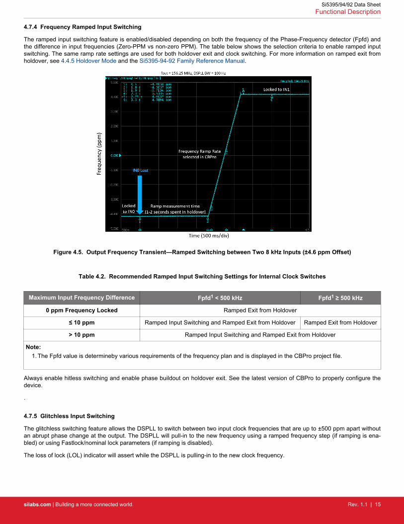
4.7.4 Frequency Ramped Input Switching
The ramped input switching feature is enabled/disabled depending on both the frequency of the Phase-Frequency detector (Fpfd) andthe difference in input frequencies (Zero-PPM vs non-zero PPM). The table below shows the selection criteria to enable ramped inputswitching. The same ramp rate settings are used for both holdover exit and clock switching. For more information on ramped exit fromholdover, see 4.4.5 Holdover Mode and the Si5395-94-92 Family Reference Manual.
Figure 4.5. Output Frequency Transient—Ramped Switching between Two 8 kHz Inputs (±4.6 ppm Offset)
Table 4.2. Recommended Ramped Input Switching Settings for Internal Clock Switches
Maximum Input Frequency Difference Fpfd1 < 500 kHz Fpfd1 ≥ 500 kHz
0 ppm Frequency Locked Ramped Exit from Holdover
≤ 10 ppm Ramped Input Switching and Ramped Exit from Holdover Ramped Exit from Holdover
> 10 ppm Ramped Input Switching and Ramped Exit from Holdover
Note:1. The Fpfd value is determineby various requirements of the frequency plan and is displayed in the CBPro project file.
Always enable hitless switching and enable phase buildout on holdover exit. See the latest version of CBPro to properly configure thedevice.
.
4.7.5 Glitchless Input Switching
The glitchless switching feature allows the DSPLL to switch between two input clock frequencies that are up to ±500 ppm apart withoutan abrupt phase change at the output. The DSPLL will pull-in to the new frequency using a ramped frequency step (if ramping is ena-bled) or using Fastlock/nominal lock parameters (if ramping is disabled).
The loss of lock (LOL) indicator will assert while the DSPLL is pulling-in to the new clock frequency.
Si5395/94/92 Data SheetFunctional Description
silabs.com | Building a more connected world. Rev. 1.1 | 15

4.7.6 Synchronizing to Gapped Input Clocks (Grade A/B/C/D and J/K/L/M Only)
The DSPLL supports locking to an input clock that has missing periods. This is also referred to as a gapped clock. The purpose ofgapped clocking is to modulate the frequency of a periodic clock by selectively removing some of its cycles. Gapping a clock severelyincreases its jitter so a phase-locked loop with high jitter tolerance and low loop bandwidth is required to produce a low-jitter periodicclock. The resulting output will be a periodic non-gapped clock with an average frequency of the input with its missing cycles. For exam-ple, an input clock of 100 MHz with one cycle removed every 10 cycles will result in a 90 MHz periodic non-gapped output clock. This isshown in the following figure. For more information on gapped clocks, see “AN561: Introduction to Gapped Clocks and PLLs”.
DSPLL
100 ns 100 ns
1 2 3 4 5 6 7 8 9 10 1 2 3 4 5 6 7 8 9
100 MHz clock1 missing period every 10
90 MHz non-gapped clock
10 ns 11.11111... ns
Gapped Input Clock Periodic Output Clock
Period Removed
Figure 4.6. Generating an Averaged Clock Output Frequency from a Gapped Clock Input
A valid gapped clock input must have a minimum frequency of 10 MHz with a maximum of two missing cycles out of every eight. Lock-ing to a gapped clock will not trigger the LOS, OOF, and LOL fault monitors. Clock switching between gapped clocks may violate thehitless switching specification in Table 5.8 Performance Characteristics on page 34 when the switch occurs during a gap in eitherinput clock.
4.8 Fault Monitoring
All four input clocks (IN0, IN1, IN2, IN3/FB_IN) are monitored for loss of signal (LOS) and out-of-frequency (OOF) as shown in the fig-ure below. The reference at the XA/XB pins is also monitored for LOS since it provides a critical reference clock for the DSPLL. There isalso a Loss Of Lock (LOL) indicator, which is asserted when the DSPLL loses synchronization.
DSPLL
LPFPD
÷M
IN0IN0b
PrecisionFastOOFLOS÷P0
IN1IN1b
PrecisionFastOOFLOS÷P1
IN3/FB_ININ3/FB_INb
PrecisionFastOOFLOS÷P3
IN2IN2b
PrecisionFastOOFLOS÷P2
LOL
XBXA
OSC
LOS
Si5395/94/92
Figure 4.7. Si5395/94/92 Fault Monitors
Si5395/94/92 Data SheetFunctional Description
silabs.com | Building a more connected world. Rev. 1.1 | 16

4.8.1 Input LOS Detection
The loss of signal monitor measures the period of each input clock cycle to detect phase irregularities or missing clock edges. Each ofthe input LOS circuits has its own programmable sensitivity which allows ignoring missing edges or intermittent errors. Loss of signalsensitivity is configurable using the ClockBuilder Pro utility. The LOS status for each of the monitors is accessible by reading a statusregister. The live LOS register always displays the current LOS state and a sticky register always stays asserted until cleared. An optionto disable any of the LOS monitors is also available.
LOSen
Monitor
LOSLOS
Sticky
Live
Figure 4.8. LOS Status Indicators
4.8.2 XA/XB LOS Detection
A LOS monitor is available to ensure that the external crystal or reference clock is valid. By default the output clocks are disabled whenXAXB_LOS is detected. This feature can be disabled such that the device will continue to produce output clocks when XAXB_LOS isdetected.
4.8.3 OOF Detection
Each input clock is monitored for frequency accuracy with respect to a OOF reference which it considers as its “0_ppm” reference. ThisOOF reference can be selected as either:• XA/XB pins• Any input clock (IN0, IN1, IN2, IN3)
The final OOF status is determined by the combination of both a precise OOF monitor and a fast OOF monitor as shown in the figurebelow. An option to disable either monitor is also available. The live OOF register always displays the current OOF state, and its stickyregister bit stays asserted until cleared.
en
en
Precision
FastOOF
Monitor
LOSOOF
Sticky
Live
Figure 4.9. OOF Status Indicator
Si5395/94/92 Data SheetFunctional Description
silabs.com | Building a more connected world. Rev. 1.1 | 17

4.8.3.1 Precision OOF Monitor
The precision OOF monitor circuit measures the frequency of all input clocks to within ±1/16 ppm accuracy with respect to the selectedOOF frequency reference. A valid input clock frequency is one that remains within the OOF frequency range which is register configura-ble up to ±512 ppm in steps of 1/16 ppm. A configurable amount of hysteresis is also available to prevent the OOF status from togglingat the failure boundary. An example is shown in the figure below. In this case, the OOF monitor is configured with a valid frequencyrange of ±6 ppm and with 2 ppm of hysteresis. An option to use one of the input pins (IN0–IN3) as the 0 ppm OOF reference instead ofthe XA/XB pins is available. This option is register configurable.
OOF Reference
Hysteresis HysteresisOOF Declared
OOF Cleared-6 ppm(Set)
-4 ppm(Clear)
0 ppm +4 ppm(Clear)
+6 ppm(Set)
fIN
Figure 4.10. Example of Precise OOF Monitor Assertion and Deassertion Triggers
4.8.3.2 Fast OOF Monitor
Because the precision OOF monitor needs to provide 1/16 ppm of frequency measurement accuracy, it must measure the monitoredinput clock frequencies over a relatively long period of time. This may be too slow to detect an input clock that is quickly ramping infrequency. An additional level of OOF monitoring called the Fast OOF monitor runs in parallel with the precision OOF monitors to quick-ly detect a ramping input frequency. The Fast OOF monitor asserts OOF on an input clock frequency that has changed by greater than±4000 ppm.
4.8.4 LOL Detection
The Loss Of Lock (LOL) monitor asserts a LOL register bit when the DSPLL has lost synchronization with its selected input clock. Thereis also a dedicated loss of lock pin that reflects the loss of lock condition. The LOL monitor functions by measuring the frequency differ-ence between the input and feedback clocks at the phase detector. There are two LOL frequency monitors, one that sets the LOL indi-cator (LOL Set) and another that clears the indicator (LOL Clear). An optional timer is available to delay clearing of the LOL indicator toallow additional time for the DSPLL to completely lock to the input clock. The timer is also useful to prevent the LOL indicator fromtoggling or chattering as the DSPLL completes lock acquisition. A block diagram of the LOL monitor is shown in the figure below. Thelive LOL register always displays the current LOL state and a sticky register always stays asserted until cleared. The LOL pin reflectsthe current state of the LOL monitor.
DSPLL
LPFPD
÷MSi5395/94/92
LOL Clear
LOL Set
Timer
LOLb
LOSLOL
Sticky
Live
LOL Monitor
fIN
Feedback Clock
Figure 4.11. LOL Status Indicators
The LOL frequency monitors have an adjustable sensitivity which is register configurable from 0.1 ppm to 10,000 ppm. Having two sep-arate frequency monitors allows for hysteresis to help prevent chattering of LOL status.
Si5395/94/92 Data SheetFunctional Description
silabs.com | Building a more connected world. Rev. 1.1 | 18

An example configuration where LOCK is indicated when there is less than 0.1 ppm frequency difference at the inputs of the phasedetector and LOL is indicated when there’s more than 1 ppm frequency difference is shown in the following figure.
Phase Detector Frequency Difference (ppm)
HysteresisLOL
LOCKED
Clear LOLThreshold
Set LOLThreshold
Lock Acquisition
0
Lost Lock
10,0000.1 1
Figure 4.12. LOL Set and Clear Thresholds
An optional timer is available to delay clearing of the LOL indicator to allow additional time for the DSPLL to completely lock to the inputclock. The timer is also useful to prevent the LOL indicator from toggling or chattering as the DSPLL completes lock acquisition. Theconfigurable delay value depends on frequency configuration and loop bandwidth of the DSPLL and is automatically calculated usingthe ClockBuilder Pro utility.
4.8.5 Interrupt Pin (INTRb)
An interrupt pin (INTRb) indicates a change in state of the status indicators (LOS, OOF, LOL, HOLD). Any of the status indicators aremaskable to prevent assertion of the interrupt pin. The state of the INTRb pin is reset by clearing the status register that caused theinterrupt.
4.9 Outputs
Each driver has a configurable voltage swing and common mode voltage covering a wide variety of differential signal formats. In addi-tion to supporting differential signals, any of the outputs can be configured as single-ended LVCMOS (3.3 V, 2.5 V, or 1.8 V) providingup to 20 single-ended outputs, or any combination of differential and single-ended outputs.
4.9.1 Grade A/B/C/D and J/K/L/M
The Si539x "standard" grades A/B/C/D (external reference) and J/K/L/M (integrated reference) can generate any output frequency inany format with best-in-class jitter. These devices are available as a preprogrammed option or can be written to the device via I2C. Theinput/output frequency plan determines whether the output divider operates in integer or fractional mode. In the fractional mode, thedevice can generate any output frequency or any format from any input frequency with best-in-class jitter. Some frequency plans allowthe user to use an integer mode that delivers even lower jitter. See the Si5395-94-92 Family Reference Manual for more details.
PHYs156.25 MHz
PHYsPHYs
Si5395A Jitter
Attenuator
Backplane Clock
19.44 MHz
PHYsPHYsPHYsPHYs
PHYs155.52 MHz
PHYsPHYsPHYsPHYsPHYsPHYs
Figure 4.13. Si5395 A/B/C/D/J/K/L/M Jitter Attenuator
Si5395/94/92 Data SheetFunctional Description
silabs.com | Building a more connected world. Rev. 1.1 | 19
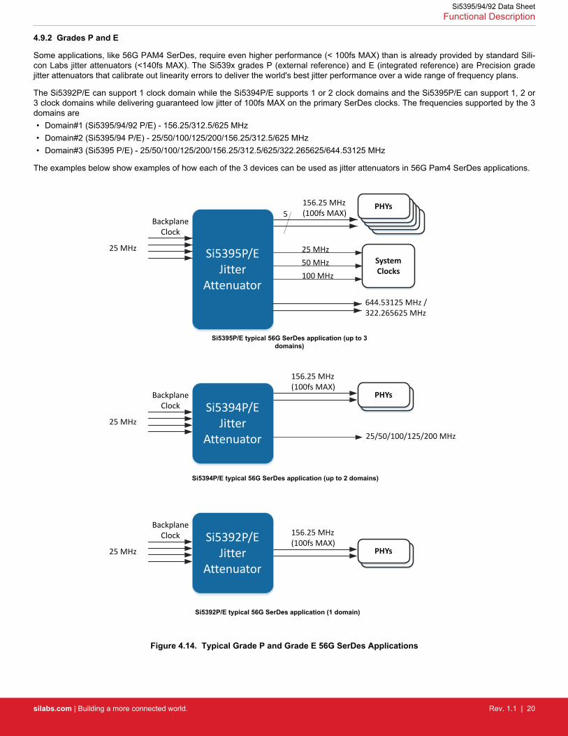
4.9.2 Grades P and E
Some applications, like 56G PAM4 SerDes, require even higher performance (< 100fs MAX) than is already provided by standard Sili-con Labs jitter attenuators (<140fs MAX). The Si539x grades P (external reference) and E (integrated reference) are Precision gradejitter attenuators that calibrate out linearity errors to deliver the world's best jitter performance over a wide range of frequency plans.
The Si5392P/E can support 1 clock domain while the Si5394P/E supports 1 or 2 clock domains and the Si5395P/E can support 1, 2 or3 clock domains while delivering guaranteed low jitter of 100fs MAX on the primary SerDes clocks. The frequencies supported by the 3domains are• Domain#1 (Si5395/94/92 P/E) - 156.25/312.5/625 MHz• Domain#2 (Si5395/94 P/E) - 25/50/100/125/200/156.25/312.5/625 MHz• Domain#3 (Si5395 P/E) - 25/50/100/125/200/156.25/312.5/625/322.265625/644.53125 MHz
The examples below show examples of how each of the 3 devices can be used as jitter attenuators in 56G Pam4 SerDes applications.
PHYs
156.25 MHz(100fs MAX)
Si5395P/E Jitter
Attenuator
Backplane Clock
25 MHz
PHYsPHYsPHYsPHYs
25 MHz
644.53125 MHz / 322.265625 MHz
5
SystemClocks
50 MHz100 MHz
156.25 MHz(100fs MAX)
Si5394P/E Jitter
Attenuator
Backplane Clock
25 MHz
PHYsPHYs
25/50/100/125/200 MHz
156.25 MHz(100fs MAX)Si5392P/E
Jitter Attenuator
Backplane Clock
25 MHz PHYsPHYs
Si5395P/E typical 56G SerDes application (up to 3 domains)
Si5394P/E typical 56G SerDes application (up to 2 domains)
Si5392P/E typical 56G SerDes application (1 domain)
Figure 4.14. Typical Grade P and Grade E 56G SerDes Applications
Si5395/94/92 Data SheetFunctional Description
silabs.com | Building a more connected world. Rev. 1.1 | 20

The external reference used on the XA/XB pins of the P grade is restricted to a 48 MHz crystal. No other values of crystal or otherreference sources like XO or VCXO are allowed. If the design requires other crystal frequencies, then the standard Si539xA/B/C/Dshould be used instead of the Si539xP.
To deliver guaranteed jitter performance 100fs MAX on the 56 G Pam4 SerDes clocks, the additional system clocks must follow somespecific design rules. Additionally, the device input clocks should be traceable back to a Stratum 3 primary reference clock. See theSi5395/94/92 Family Reference manual for more details on these design rules.
4.9.3 Output Crosspoint
A crosspoint allows any of the output drivers to connect with any of the MultiSynths. The crosspoint configuration is programmable andcan be stored in NVM so that the desired output configuration is ready at power up.
4.9.4 Output Signal Format
The differential output swing and common mode voltage are both fully programmable covering a wide variety of signal formats includingLVDS and LVPECL. In addition to supporting differential signals, any of the outputs can be configured as LVCMOS (3.3 V, 2.5 V, or 1.8V) drivers providing up to 20 single-ended outputs, or any combination of differential and single-ended outputs.
4.9.5 Programmable Common Mode Voltage For Differential Outputs
The common mode voltage (VCM) for the differential modes are programmable so that LVDS specifications can be met and for the bestsignal integrity with different supply voltages. When DC coupling the output driver, it is essential that the receiver have a relatively highcommon mode impedance so that the common mode current from the output driver is very small.
4.9.6 LVCMOS Output Impedance Selection
Each LVCMOS driver has a configurable output impedance to accommodate different trace impedances. A source termination resistoris recommended to help match the selected output impedance to the trace impedance, where Rs = Transmission line impedance – ZO.There are three programmable output impedance selections (CMOS1, CMOS2, CMOS3) for each VDDO option as shown in the follow-ing table.
Table 4.3. Typical Output Impedance (ZS)
VDDO CMOS Drive Selections
OUTx_CMOS_DRV = 1 OUTx_CMOS_DRV = 2 OUTx_CMOS_DRV = 3
3.3 V 38 Ω 30 Ω 22 Ω
2.5 V 43 Ω 35 Ω 24 Ω
1.8 V — 46 Ω 31 Ω
4.9.7 LVCMOS Output Signal Swing
The signal swing (VOL/VOH) of the LVCMOS output drivers is set by the voltage on the VDDO pins. Each output driver has its ownVDDO pin allowing a unique output voltage swing for each of the LVCMOS drivers.
4.9.8 LVCMOS Output Polarity
When a driver is configured as an LVCMOS output, it generates a clock signal on both pins (OUTx and OUTxb). By default, the clockon the OUTx pin is generated with the same polarity (in phase) as the clock on the OUTxb pin. The polarity of these clocks is configura-ble, enabling complementary clock generation and/or inverted polarity with respect to other output drivers.
4.9.9 Output Enable/Disable
The OEb pin provides a convenient method of disabling or enabling the output drivers. When the OEb pin is held high, all outputs aredisabled. When held low, the outputs are enabled. Outputs in the enabled state can be individually disabled through register control.
Si5395/94/92 Data SheetFunctional Description
silabs.com | Building a more connected world. Rev. 1.1 | 21

4.9.10 Output Driver State When Disabled
The disabled state of an output driver is configurable as disable low or disable high.
4.9.11 Synchronous Output Disable Feature
The output drivers provide a selectable synchronous disable feature. Output drivers with this feature turned on will wait until a clockperiod has completed before the driver is disabled. This prevents unwanted runt pulses from occurring when disabling an output. Whenthis feature is turned off, the output clock will disable immediately without waiting for the period to complete.
4.9.12 Input/Output Skew Control
The input-output skew can be adjusted in dynamic mode. The dynamic phase adjust will allow the device to dynamically and glitchlesslychange the output phase using register writes with the device still powered up. The skew value may change after each reset or powercycle. See the family reference manual for more details.
4.9.13 Zero Delay Mode
A zero delay mode is available for applications that require fixed and consistent minimum delay between the selected input and outputs.The zero delay mode is configured by opening the internal feedback loop through software configuration and closing the loop externallyas shown in the figure below. (Zero delay mode is only available for clock inputs that are higher than 128 kHz.)
This helps to cancel out the internal delay introduced by the dividers, the crosspoint, the input, and the output drivers. Any one of theoutputs can be fed back to the FB_IN pins, although using the output driver that achieves the shortest trace length will help to minimizethe input-to-output delay. The OUT9 and FB_IN pins are recommended for the external feedback connection. The FB_IN input pinsmust be terminated and ac-coupled when zero delay mode is used. A differential external feedback path connection is necessary forbest performance. Note that the hitless switching feature is not available when zero delay mode is enabled.
VDDO7
OUT7bOUT7÷R7
OUT0bOUT0÷R0
IN0IN0b
IN1IN1b
IN2IN2b
÷P1
÷P0
÷P2
DSPLL
LPFPD
÷MIN3/FB_IN
÷P3
100
IN3/FB_INb
÷N0 t0
÷N1 t1
÷N2 t2
÷N3 t3
÷N4 t4
OUT2b
VDDO2OUT2÷R2
External Feedback Path
OUT1b
VDDO1OUT1÷R1
OUT8b
VDDO8OUT8÷R8
OUT9bOUT9
÷R9
OUT0Ab
VDDO0
OUT0A÷R0A
OUT9AbOUT9A
÷R9A
VDDO9
÷5
Figure 4.15. Si5395 Zero Delay Mode Setup
Si5395/94/92 Data SheetFunctional Description
silabs.com | Building a more connected world. Rev. 1.1 | 22

4.9.14 Output Divider (R) Synchronization
All the output R dividers are reset to a known state during the power-up initialization period. This ensures consistent and repeatablephase alignment across all output drivers that are connected to the same N divider.
4.10 Power Management
Unused inputs and output drivers can be powered down when unused. Consult the Si5395-94-92 Family Reference Manual and Clock-Builder Pro configuration utility for details.
4.11 In-Circuit Programming
The Si5395/94/92 is fully configurable using the serial interface (I2C or SPI). At power-up the device downloads its default register val-ues from internal non-volatile memory (NVM). Application specific default configurations can be written into NVM allowing the device togenerate specific clock frequencies at power-up. Writing default values to NVM is in-circuit programmable with normal operating powersupply voltages applied to its VDD and VDDA pins. The NVM is two time writable. Once a new configuration has been written to NVM,the old configuration is no longer accessible. Refer to the Si5395-94-92 Family Reference Manual for a detailed procedure for writingregisters to NVM.
4.12 Serial Interface
Configuration and operation of the Si5395/94/92 is controlled by reading and writing registers using the I2C or SPI interface. TheI2C_SEL pin selects I2C or SPI operation. Communication with both 3.3 V and 1.8 V host is supported. The SPI mode operates ineither 4-wire or 3-wire. See the Si5395-94-92 Family Reference Manual for details.
4.13 Custom Factory Preprogrammed Parts
For applications where a serial interface is not available for programming the device, custom pre-programmed parts can be orderedwith a specific configuration written into NVM. A factory preprogrammed part will generate clocks at power-up. Custom, factory-preprog-rammed devices are available. The ClockBuilder Pro custom part number wizard can be used to quickly and easily generate a custompart number for your configuration.
In less than three minutes, you will be able to generate a custom part number with a detailed data sheet addendum matching yourdesign’s configuration. Once you receive the confirmation email with the data sheet addendum, simply place an order with your localSilicon Labs sales representative. Samples of your preprogrammed device will typically ship in about two weeks.
4.14 Register Map
The register map is divided into multiple pages where each page has 256 addressable registers. Page 0 contains frequently accessibleregisters, such as alarm status, resets, device identification, etc. Other pages contain registers that need less frequent access such asfrequency configuration, and general device settings. Refer to the Si5395-94-92 Family Reference Manual for a complete list of registerdescriptions and settings. It is strongly recommended that ClockBuilder Pro be used to create and manage register settings.
Si5395/94/92 Data SheetFunctional Description
silabs.com | Building a more connected world. Rev. 1.1 | 23

5. Electrical Specifications
Table 5.1. Recommended Operating Conditions1
Parameter Symbol Min Typ Max Unit
Ambient Temperature TA –40 25 85 °C
Junction Temperature TJMAX — — 125 °C
Core Supply VoltageVDD 1.71 1.80 1.89 V
VDDA 3.14 3.30 3.47 V
Clock Output Driver Supply Voltage VDDO
3.14 3.30 3.47 V
2.37 2.50 2.62 V
1.71 1.80 1.89 V
Status Pin Supply Voltage VDDS3.14 3.30 3.47 V
1.71 1.80 1.89 V
Note:1. All minimum and maximum specifications are guaranteed and apply across the recommended operating conditions. Typical val-
ues apply at nominal supply voltages and an operating temperature of 25 °C unless otherwise noted.
Si5395/94/92 Data SheetElectrical Specifications
silabs.com | Building a more connected world. Rev. 1.1 | 24
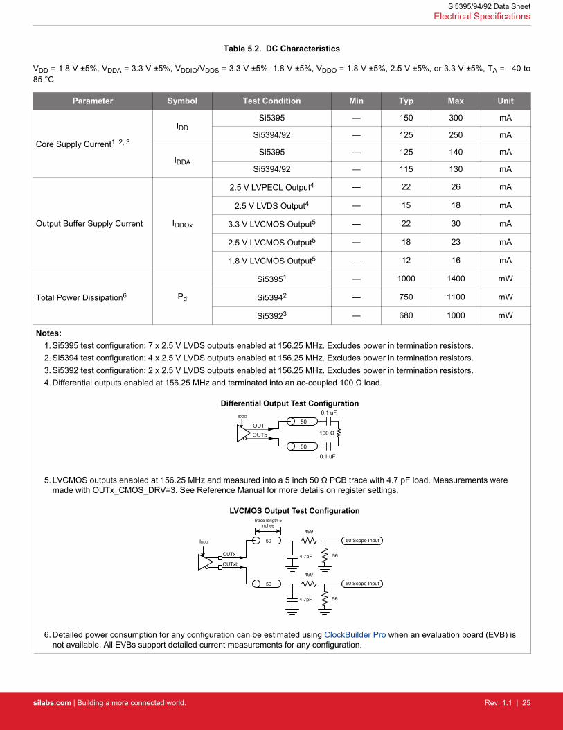
Table 5.2. DC Characteristics
VDD = 1.8 V ±5%, VDDA = 3.3 V ±5%, VDDIO/VDDS = 3.3 V ±5%, 1.8 V ±5%, VDDO = 1.8 V ±5%, 2.5 V ±5%, or 3.3 V ±5%, TA = –40 to85 °C
Parameter Symbol Test Condition Min Typ Max Unit
Core Supply Current1, 2, 3
IDDSi5395 — 150 300 mA
Si5394/92 — 125 250 mA
IDDASi5395 — 125 140 mA
Si5394/92 — 115 130 mA
Output Buffer Supply Current IDDOx
2.5 V LVPECL Output4 — 22 26 mA
2.5 V LVDS Output4 — 15 18 mA
3.3 V LVCMOS Output5 — 22 30 mA
2.5 V LVCMOS Output5 — 18 23 mA
1.8 V LVCMOS Output5 — 12 16 mA
Total Power Dissipation6 Pd
Si53951 — 1000 1400 mW
Si53942 — 750 1100 mW
Si53923 — 680 1000 mW
Notes:1. Si5395 test configuration: 7 x 2.5 V LVDS outputs enabled at 156.25 MHz. Excludes power in termination resistors.2. Si5394 test configuration: 4 x 2.5 V LVDS outputs enabled at 156.25 MHz. Excludes power in termination resistors.3. Si5392 test configuration: 2 x 2.5 V LVDS outputs enabled at 156.25 MHz. Excludes power in termination resistors.4. Differential outputs enabled at 156.25 MHz and terminated into an ac-coupled 100 Ω load.
50
50
100 Ω OUT
OUTb
IDDO 0.1 uF
0.1 uF
Differential Output Test Configuration
5. LVCMOS outputs enabled at 156.25 MHz and measured into a 5 inch 50 Ω PCB trace with 4.7 pF load. Measurements weremade with OUTx_CMOS_DRV=3. See Reference Manual for more details on register settings.
OUTx
OUTxb
IDDO
499
564.7pF
50 Scope Input50
499
564.7pF
50 Scope Input50
Trace length 5inches
LVCMOS Output Test Configuration
6. Detailed power consumption for any configuration can be estimated using ClockBuilder Pro when an evaluation board (EVB) isnot available. All EVBs support detailed current measurements for any configuration.
Si5395/94/92 Data SheetElectrical Specifications
silabs.com | Building a more connected world. Rev. 1.1 | 25
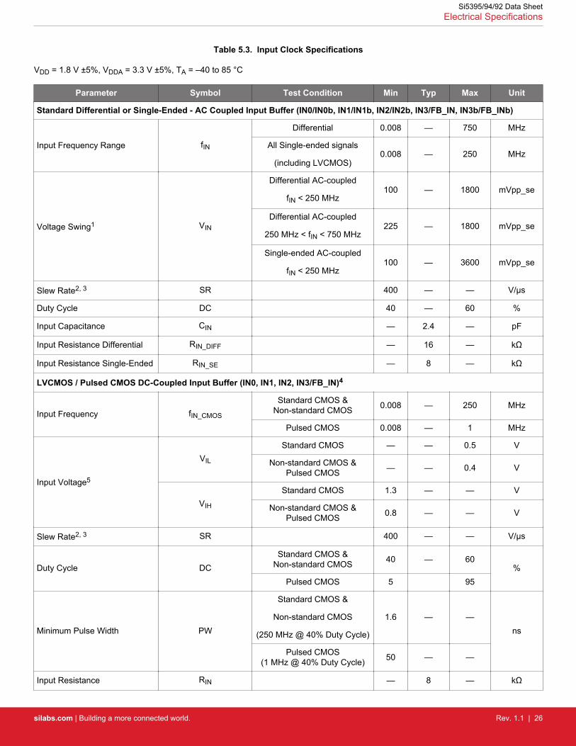
Table 5.3. Input Clock Specifications
VDD = 1.8 V ±5%, VDDA = 3.3 V ±5%, TA = –40 to 85 °C
Parameter Symbol Test Condition Min Typ Max Unit
Standard Differential or Single-Ended - AC Coupled Input Buffer (IN0/IN0b, IN1/IN1b, IN2/IN2b, IN3/FB_IN, IN3b/FB_INb)
Input Frequency Range fIN
Differential 0.008 — 750 MHz
All Single-ended signals
(including LVCMOS)0.008 — 250 MHz
Voltage Swing1 VIN
Differential AC-coupled
fIN < 250 MHz100 — 1800 mVpp_se
Differential AC-coupled
250 MHz < fIN < 750 MHz225 — 1800 mVpp_se
Single-ended AC-coupled
fIN < 250 MHz100 — 3600 mVpp_se
Slew Rate2, 3 SR 400 — — V/µs
Duty Cycle DC 40 — 60 %
Input Capacitance CIN — 2.4 — pF
Input Resistance Differential RIN_DIFF — 16 — kΩ
Input Resistance Single-Ended RIN_SE — 8 — kΩ
LVCMOS / Pulsed CMOS DC-Coupled Input Buffer (IN0, IN1, IN2, IN3/FB_IN)4
Input Frequency fIN_CMOS
Standard CMOS &Non-standard CMOS 0.008 — 250 MHz
Pulsed CMOS 0.008 — 1 MHz
Input Voltage5
VIL
Standard CMOS — — 0.5 V
Non-standard CMOS &Pulsed CMOS — — 0.4 V
VIH
Standard CMOS 1.3 — — V
Non-standard CMOS &Pulsed CMOS 0.8 — — V
Slew Rate2, 3 SR 400 — — V/µs
Duty Cycle DCStandard CMOS &
Non-standard CMOS 40 — 60%
Pulsed CMOS 5 95
Minimum Pulse Width PW
Standard CMOS &
Non-standard CMOS
(250 MHz @ 40% Duty Cycle)
1.6 — —ns
Pulsed CMOS(1 MHz @ 40% Duty Cycle) 50 — —
Input Resistance RIN — 8 — kΩ
Si5395/94/92 Data SheetElectrical Specifications
silabs.com | Building a more connected world. Rev. 1.1 | 26
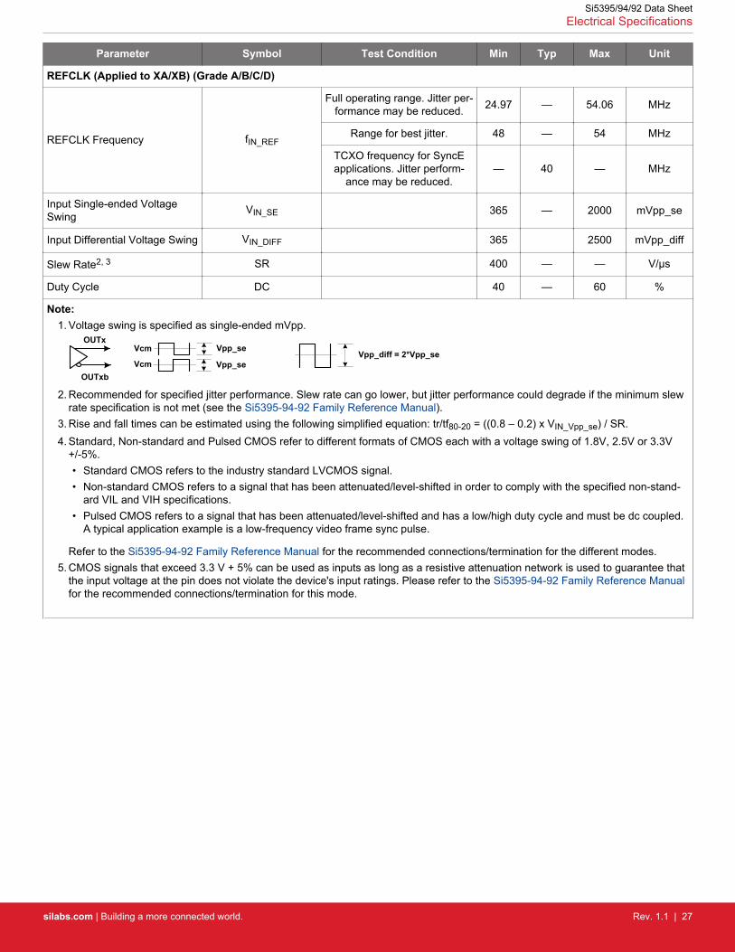
Parameter Symbol Test Condition Min Typ Max Unit
REFCLK (Applied to XA/XB) (Grade A/B/C/D)
REFCLK Frequency fIN_REF
Full operating range. Jitter per-formance may be reduced. 24.97 — 54.06 MHz
Range for best jitter. 48 — 54 MHz
TCXO frequency for SyncEapplications. Jitter perform-
ance may be reduced.— 40 — MHz
Input Single-ended VoltageSwing
VIN_SE 365 — 2000 mVpp_se
Input Differential Voltage Swing VIN_DIFF 365 2500 mVpp_diff
Slew Rate2, 3 SR 400 — — V/µs
Duty Cycle DC 40 — 60 %
Note:1. Voltage swing is specified as single-ended mVpp.
OUTxb
OUTxVpp_se
Vpp_seVpp_diff = 2*Vpp_se
Vcm
Vcm
2. Recommended for specified jitter performance. Slew rate can go lower, but jitter performance could degrade if the minimum slewrate specification is not met (see the Si5395-94-92 Family Reference Manual).
3. Rise and fall times can be estimated using the following simplified equation: tr/tf80-20 = ((0.8 – 0.2) x VIN_Vpp_se) / SR.4. Standard, Non-standard and Pulsed CMOS refer to different formats of CMOS each with a voltage swing of 1.8V, 2.5V or 3.3V
+/-5%.• Standard CMOS refers to the industry standard LVCMOS signal.• Non-standard CMOS refers to a signal that has been attenuated/level-shifted in order to comply with the specified non-stand-
ard VIL and VIH specifications.• Pulsed CMOS refers to a signal that has been attenuated/level-shifted and has a low/high duty cycle and must be dc coupled.
A typical application example is a low-frequency video frame sync pulse.
Refer to the Si5395-94-92 Family Reference Manual for the recommended connections/termination for the different modes.5. CMOS signals that exceed 3.3 V + 5% can be used as inputs as long as a resistive attenuation network is used to guarantee that
the input voltage at the pin does not violate the device's input ratings. Please refer to the Si5395-94-92 Family Reference Manualfor the recommended connections/termination for this mode.
Si5395/94/92 Data SheetElectrical Specifications
silabs.com | Building a more connected world. Rev. 1.1 | 27
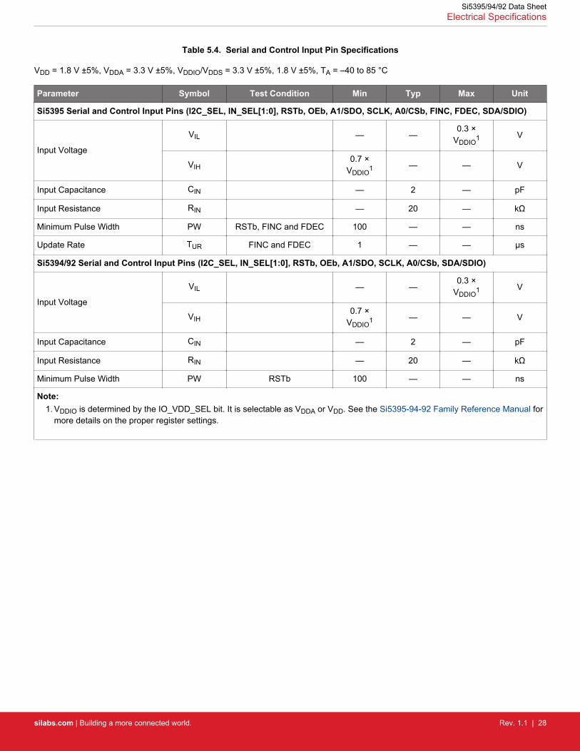
Table 5.4. Serial and Control Input Pin Specifications
VDD = 1.8 V ±5%, VDDA = 3.3 V ±5%, VDDIO/VDDS = 3.3 V ±5%, 1.8 V ±5%, TA = –40 to 85 °C
Parameter Symbol Test Condition Min Typ Max Unit
Si5395 Serial and Control Input Pins (I2C_SEL, IN_SEL[1:0], RSTb, OEb, A1/SDO, SCLK, A0/CSb, FINC, FDEC, SDA/SDIO)
Input Voltage
VIL — —0.3 ×
VDDIO1 V
VIH0.7 ×
VDDIO1 — — V
Input Capacitance CIN — 2 — pF
Input Resistance RIN — 20 — kΩ
Minimum Pulse Width PW RSTb, FINC and FDEC 100 — — ns
Update Rate TUR FINC and FDEC 1 — — µs
Si5394/92 Serial and Control Input Pins (I2C_SEL, IN_SEL[1:0], RSTb, OEb, A1/SDO, SCLK, A0/CSb, SDA/SDIO)
Input Voltage
VIL — —0.3 ×
VDDIO1 V
VIH0.7 ×
VDDIO1 — — V
Input Capacitance CIN — 2 — pF
Input Resistance RIN — 20 — kΩ
Minimum Pulse Width PW RSTb 100 — — ns
Note:1. VDDIO is determined by the IO_VDD_SEL bit. It is selectable as VDDA or VDD. See the Si5395-94-92 Family Reference Manual for
more details on the proper register settings.
Si5395/94/92 Data SheetElectrical Specifications
silabs.com | Building a more connected world. Rev. 1.1 | 28

Table 5.5. Differential Clock Output Specifications
VDD = 1.8 V ±5%, VDDA = 3.3 V ±5%, VDDO = 1.8 V ±5%, 2.5 V ±5%, or 3.3 V ±5%, TA = –40 to 85 °C
Parameter Symbol Test Condition Min Typ Max Unit
Si5395/94/92
Output Frequency fOUTMultiSynth not used
0.0001 — 720 MHz
733.33 — 800.00 MHz
825 — 1028 MHz
MultiSynth used 0.0001 — 720 MHz
Duty Cycle1 DC
MultiSynth used:
fOUT < 400 MHz48 — 52 %
MultiSynth used:
400 MHz < fOUT <= 720MHz
45 — 55 %
MultiSynth not used:
fOUT < 1028 MHz
25 — 75 %
Output Voltage Swing2 VOUT
VDDO = 3.3 V,2.5 V, 1.8 V LVDS 350 450 530 mVpp_se
VDDO = 3.3 V,2.5 V
LVPECL 630 780 950 mVpp_se
Common Mode Voltage2, 3
(100 Ω load line-to-line)VCM
VDDO = 3.3 VLVDS 1.1 1.2 1.3 V
LVPECL 1.9 2.0 2.1 V
VDDO = 2.5 VLVPECL
LVDS1.1 1.2 1.3 V
VDDO = 1.8 V sub-LVDS 0.8 0.9 1.0 V
Output-to-Output Skew(Same MultiSynth)
TSKSfOUT = 712.5 MHz
(LVDS)— 0 75 ps
Out-Outb Skew on one output TSK_OUT Measured from positive tonegative output pins (LVDS) — 0 50 ps
Rise and Fall Times2 tr/tffOUT > 100 MHz (20% to
80%)— 100 200 ps
Differential Output Impedance ZO — 100 — Ω
Power Supply Noise Rejec-tion3 PSRR
10 kHz sinusoidal noise — –101 — dBc
100 kHz sinusoidal noise — –96 — dBc
500 kHz sinusoidal noise — –99 — dBc
1 MHz sinusoidal noise — –97 — dBc
Output-to-Output Crosstalk4 XTALKSi5395 — –72 — dBc
Si5394/92 — –88 — dBc
Si5395/94/92 Data SheetElectrical Specifications
silabs.com | Building a more connected world. Rev. 1.1 | 29

Parameter Symbol Test Condition Min Typ Max Unit
Notes:1. Duty cycle can vary depending on frequency plan (output frequency and divide ratios).2. Output amplitude and common-mode settings are programmable through register settings and can be stored in NVM. Each out-
put driver can be programmed independently. Note that the maximum LVDS single-ended amplitude can be up to 110 mV higherthan the TIA/EIA-644 maximum. Refer to the Si5395-94-92 Family Reference Manual for more suggested output settings. Not allcombinations of voltage amplitude and common mode voltages settings are possible.
OUTxb
OUTxVpp_se
Vpp_seVpp_diff = 2*Vpp_se
Vcm
Vcm
50
50
100 Ω OUT
OUTb
IDDO 0.1 uF
0.1 uF
Differential Output Test Configuration
3. Measured for 156.25 MHz carrier frequency. 100 mVpp sinewave noise added to VDDO = 3.3 V and noise spur amplitude meas-ured.
4. Measured across two adjacent outputs, both in LVDS mode, with the victim running at 155.52 MHz and the aggressor at 156.25MHz. Refer to “AN862: Optimizing Si534x Jitter Performance in Next Generation Internet Infrastructure Systems” for guidance oncrosstalk optimization. Note that all active outputs must be terminated when measuring crosstalk.
Si5395/94/92 Data SheetElectrical Specifications
silabs.com | Building a more connected world. Rev. 1.1 | 30

Table 5.6. LVCMOS Clock Output Specifications
VDD = 1.8 V ±5%, VDDA = 3.3 V ±5%, VDDO = 1.8 V ±5%, 2.5 V ±5%, or 3.3 V ±5%, TA = –40 to 85 °C
Parameter Symbol Test Condition Min Typ Max Unit
Output Frequency fOUT 0.0001 — 250 MHz
Duty Cycle DCfOUT <100 MHz 48 — 52 %
100 MHz < fOUT < 250 MHz 44 — 56 %
Output Voltage High1, 2, 3 VOH
VDDO = 3.3 V
OUTx_CMOS_DRV = 1 IOH = –10 mA VDDO x 0.85 — — V
OUTx_CMOS_DRV = 2 IOH = –12 mA VDDO x 0.85 — — V
OUTx_CMOS_DRV = 3 IOH = –17 mA VDDO x 0.85 — — V
VDDO = 2.5 V
OUTx_CMOS_DRV = 1 IOH = –6 mA VDDO x 0.85 — — V
OUTx_CMOS_DRV = 2 IOH = –8 mA VDDO x 0.85 — — V
OUTx_CMOS_DRV = 3 IOH = –11 mA VDDO x 0.85 — — V
VDDO = 1.8 V
OUTx_CMOS_DRV = 2 IOH = –4 mA VDDO x 0.85 — — V
OUTx_CMOS_DRV = 3 IOH = –5 mA VDDO x 0.85 — — V
Output Voltage Low1, 2, 3 VOL
VDDO = 3.3 V
OUTx_CMOS_DRV = 1 IOL = 10 mA — — VDDO x 0.15 V
OUTx_CMOS_DRV = 2 IOL = 12 mA — — VDDO x 0.15 V
OUTx_CMOS_DRV = 3 IOL = 17 mA — — VDDO x 0.15 V
VDDO = 2.5 V
OUTx_CMOS_DRV = 1 IOL = 6 mA — — VDDO x 0.15 V
OUTx_CMOS_DRV = 2 IOL = 8 mA — — VDDO x 0.15 V
OUTx_CMOS_DRV = 3 IOL = 11 mA — — VDDO x 0.15 V
VDDO = 1.8 V
OUTx_CMOS_DRV = 2 IOL = 4 mA — — VDDO x 0.15 V
OUTx_CMOS_DRV = 3 IOL = 5 mA — — VDDO x 0.15 V
Rise and Fall Times3 tr/tf (20% to 80%)
VDDO = 3.3V — 400 600 ps
VDDO = 2.5 V — 450 600 ps
VDDO = 1.8 V — 550 750 ps
Si5395/94/92 Data SheetElectrical Specifications
silabs.com | Building a more connected world. Rev. 1.1 | 31

Parameter Symbol Test Condition Min Typ Max Unit
Note:1. Driver strength is a register programmable setting and stored in NVM. Options are OUTx_CMOS_DRV = 1, 2, 3. Refer to the
Si5395-94-92 Family Reference Manual for more details on register settings.2. IOL/IOH is measured at VOL/VOH as shown in the DC test configuration.
Zs
IOL/IOH
VOL/VOH
IDDO
DC Test Configuration
3. A series termination resistor (Rs) is recommended to help match the source impedance to a 50 Ω PCB trace. A 4.7 pF capacitiveload is assumed. The LVCMOS outputs were set to OUTx_CMOS_DRV = 3, at 156.25 MHz.
OUTx
OUTxb
IDDO
499
564.7pF
50 Scope Input50
499
564.7pF
50 Scope Input50
Trace length 5inches
LVCMOS Output Test Configuration
Si5395/94/92 Data SheetElectrical Specifications
silabs.com | Building a more connected world. Rev. 1.1 | 32

Table 5.7. Output Status Pin Specifications
VDD = 1.8 V ±5%, VDDA = 3.3 V ±5%, VDDIO/VDDS = 3.3 V ±5%, 1.8 V ±5%, TA = –40 to 85 °C
Parameter Symbol Test Condition Min Typ Max Unit
Si5395 Status Output Pins (LOLb, INTRb, SDA/SDIO1, SDO)
Output Voltage
VOH IOH = –2 mA VDDIO2 x
0.85— — V
VOL IOL = 2 mA — — VDDIO2 x
0.15V
Si5394/92 Status Output Pins (INTRb, SDA/SDIO11, SDO)
Output Voltage
VOH IOH = –2 mA VDDIO2 x
0.85— — V
VOL IOL = 2 mA — — VDDIO2 x
0.15V
Si5394 Status Output Pins (LOLb, LOS_XAXBb)
Si5392 Status Output Pins (LOLb, LOS_XAXBb, LOS0b, LOS1b, LOS2b, LOS3b)
Output VoltageVOH IOH = –2 mA VDDS x 0.85 — — V
VOL IOL = 2 mA — — VDDS x 0.15 V
Notes:1. The VOH specification does not apply to the open-drain SDA/SDIO output when the serial interface is in I2C mode or is unused
with I2C_SEL pulled high. VOL remains valid in all cases.2. VDDIO is determined by the IO_VDD_SEL bit. It is selectable as VDDA or VDD. See the Si5395-94-92 Family Reference Manual for
more details on the proper register settings.
Si5395/94/92 Data SheetElectrical Specifications
silabs.com | Building a more connected world. Rev. 1.1 | 33
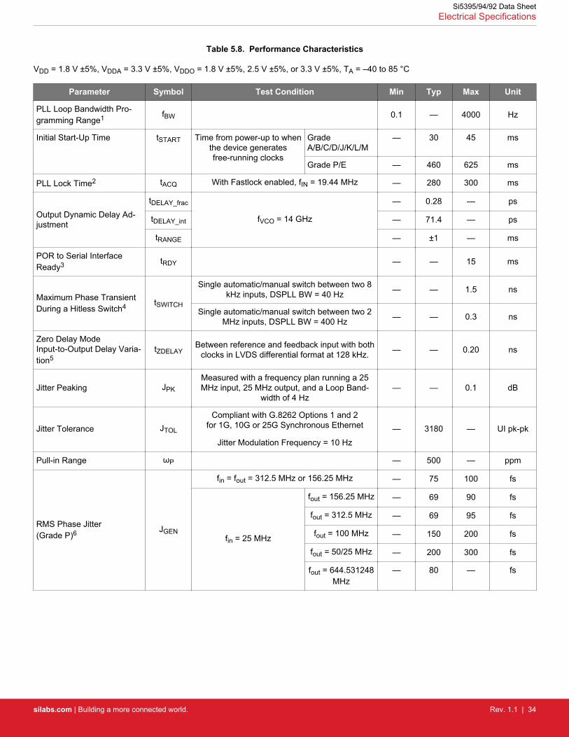
Table 5.8. Performance Characteristics
VDD = 1.8 V ±5%, VDDA = 3.3 V ±5%, VDDO = 1.8 V ±5%, 2.5 V ±5%, or 3.3 V ±5%, TA = –40 to 85 °C
Parameter Symbol Test Condition Min Typ Max Unit
PLL Loop Bandwidth Pro-gramming Range1 fBW 0.1 — 4000 Hz
Initial Start-Up Time tSTART Time from power-up to whenthe device generatesfree-running clocks
GradeA/B/C/D/J/K/L/M
— 30 45 ms
Grade P/E — 460 625 ms
PLL Lock Time2 tACQ With Fastlock enabled, fIN = 19.44 MHz — 280 300 ms
Output Dynamic Delay Ad-justment
tDELAY_frac
fVCO = 14 GHz
— 0.28 — ps
tDELAY_int — 71.4 — ps
tRANGE — ±1 — ms
POR to Serial InterfaceReady3 tRDY — — 15 ms
Maximum Phase TransientDuring a Hitless Switch4 tSWITCH
Single automatic/manual switch between two 8kHz inputs, DSPLL BW = 40 Hz — — 1.5 ns
Single automatic/manual switch between two 2MHz inputs, DSPLL BW = 400 Hz — — 0.3 ns
Zero Delay ModeInput-to-Output Delay Varia-tion5
tZDELAYBetween reference and feedback input with both
clocks in LVDS differential format at 128 kHz. — — 0.20 ns
Jitter Peaking JPK
Measured with a frequency plan running a 25MHz input, 25 MHz output, and a Loop Band-
width of 4 Hz— — 0.1 dB
Jitter Tolerance JTOL
Compliant with G.8262 Options 1 and 2for 1G, 10G or 25G Synchronous Ethernet
Jitter Modulation Frequency = 10 Hz— 3180 — UI pk-pk
Pull-in Range ωP — 500 — ppm
RMS Phase Jitter(Grade P)6
JGEN
fin = fout = 312.5 MHz or 156.25 MHz — 75 100 fs
fin = 25 MHz
fout = 156.25 MHz — 69 90 fs
fout = 312.5 MHz — 69 95 fs
fout = 100 MHz — 150 200 fs
fout = 50/25 MHz — 200 300 fs
fout = 644.531248MHz
— 80 — fs
Si5395/94/92 Data SheetElectrical Specifications
silabs.com | Building a more connected world. Rev. 1.1 | 34

Parameter Symbol Test Condition Min Typ Max Unit
RMS Phase Jitter(Grade E)6
JGEN
fin = fout = 312.5 MHz or 156.25 MHz — 82 110 fs
fin = 25 MHz
fout = 156.25 MHz — 71 100 fs
fout = 312.5 MHz — 75 105 fs
fout = 100 MHz — 150 200 fs
fout = 50/25 MHz — 200 300 fs
fout = 644.531248MHz
— 85 — fs
RMS Phase Jitter(Grade A/B/C/D andJ/K/L/M)7
JGEN
Output divider Integer Mode — 85 120 fs
Output divider Fractional Mode/DCO Mode — 115 170 fs
Note:1. Actual loop bandwidth might be lower; please refer to CBPro for actual value for your frequency plan.2. Lock Time can vary significantly depending on several parameters, such as bandwidths, LOL thresholds, etc. For this case, lock
time was measured with nominal bandwidth set to 100 Hz, fastlock bandwidth set to 1 kHz, LOL set/clear thresholds of 6/0.6 ppmrespectively, using IN0 as clock reference by removing the reference and enabling it again, then measuring the delta time be-tween the first rising edge of the clock reference and the LOL indicator deassertion.
3. Measured as time from valid VDD/VDDA rails (90% of their value) to when the serial interface is ready to respond to commands.4. Higher input frequencies will typically result in higher Fpfd frequencies, which, in turn, will result in better hitless switching per-
formance. It is recommended to use higher input frequencies for the best hitless switching performance.5. Zero-Delay-Mode is dependent on frequency configuration. Using Fpfd < 128 kHz will result in higher delay values. Ref clock rise
time must be <200 ps. Initial Start-Up time can be much higher in Zero Delay mode.6. Grade P and E are calibrated for optimum performance in 56G/112G SerDes applications at frequencies of 312.5 MHz or 156.25
MHz. Specific layout rules must be followed to achieve optimum performance. For more details, refer to 4.9.2 Grades P and Eand the reference manual.
7. Grades A/B/C/D and J/K/L/M are targeted for applications that require more flexibility and set the output divider to Integer or Frac-tional modes. Integer mode test conditions: fin = 19.44 MHz; fout = 155.52 MHz. Fractional mode test conditions: fin = 19.44 MHz;fout = 125 MHz. All outputs are assumed to be LVPECL. For more details, refer to 4.9.1 Grade A/B/C/D and J/K/L/M.
Table 5.9. I2C Timing Specifications (SCL, SDA)
VDD= 1.8 V ±5%, VDDA= 3.3 V ±5%, VDDS/VDDIO= 3.3 V ±5%, 1.8 V ±5%, TA= –40 to 85 °C
Parameter Symbol Test ConditionStandard Mode
100 kbpsFast Mode400 kbps Unit
Min Max Min Max
SCL Clock Frequency fSCL — 100 — 400 kHz
SMBus Timeout — 25 35 25 35 ms
Hold time (Repeated)START condition
tHD:STA 4.0 — 0.6 — µs
Low Period of the SCL Clock tLOW 4.7 — 1.3 — µs
HIGH Period of the SCLClock
tHIGH 4.0 — 0.6 — µs
Setup Time for a RepeatedSTART Condition
tSU:STA 4.7 — 0.6 — µs
Data Hold Time tHD:DAT 100 — 100 — ns
Data Setup Time tSU:DAT 250 — 100 — ns
Si5395/94/92 Data SheetElectrical Specifications
silabs.com | Building a more connected world. Rev. 1.1 | 35

Parameter Symbol Test ConditionStandard Mode
100 kbpsFast Mode400 kbps Unit
Min Max Min Max
Rise Time of both SDA andSCL Signals
tr — 1000 20 300 ns
Fall Time of both SDA andSCL Signals
tf — 300 — 300 ns
Setup Time for STOP Condi-tion
tSU:STO 4.0 — 0.6 — µs
Bus Free Time between aSTOP and START Condition
tBUF 4.7 — 1.3 — µs
Data Valid Time tVD:DAT — 3.45 — 0.9 µs
Data Valid AcknowledgeTime
tVD:ACK — 3.45 — 0.9 µs
Figure 5.1. I2C Serial Port Timing Standard and Fast Modes
Si5395/94/92 Data SheetElectrical Specifications
silabs.com | Building a more connected world. Rev. 1.1 | 36
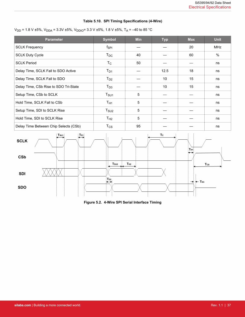
Table 5.10. SPI Timing Specifications (4-Wire)
VDD = 1.8 V ±5%, VDDA = 3.3V ±5%, VDDIO= 3.3 V ±5%, 1.8 V ±5%, TA = –40 to 85 °C
Parameter Symbol Min Typ Max Unit
SCLK Frequency fSPI — — 20 MHz
SCLK Duty Cycle TDC 40 — 60 %
SCLK Period TC 50 — — ns
Delay Time, SCLK Fall to SDO Active TD1 — 12.5 18 ns
Delay Time, SCLK Fall to SDO TD2 — 10 15 ns
Delay Time, CSb Rise to SDO Tri-State TD3 — 10 15 ns
Setup Time, CSb to SCLK TSU1 5 — — ns
Hold Time, SCLK Fall to CSb TH1 5 — — ns
Setup Time, SDI to SCLK Rise TSU2 5 — — ns
Hold Time, SDI to SCLK Rise TH2 5 — — ns
Delay Time Between Chip Selects (CSb) TCS 95 — — ns
SCLK
CSb
SDI
SDO
TSU1 TD1
TSU2
TD2
TC
TCS
TD3
TH2
TH1
Figure 5.2. 4-Wire SPI Serial Interface Timing
Si5395/94/92 Data SheetElectrical Specifications
silabs.com | Building a more connected world. Rev. 1.1 | 37

Table 5.11. SPI Timing Specifications (3-Wire)
VDD = 1.8 V ±5%, VDDA = 3.3V ±5%, VDDIO= 3.3 V ±5%, 1.8 V ±5%, TA = –40 to 85 °C
Parameter Symbol Min Typ Max Unit
SCLK Frequency fSPI — — 20 MHz
SCLK Duty Cycle TDC 40 — 60 %
SCLK Period TC 50 — — ns
Delay Time, SCLK Fall to SDIO Turn-on TD1 — 12.5 18 ns
Delay Time, SCLK Fall to SDIO Next-bit TD2 — 10 15 ns
Delay Time, CSb Rise to SDIO Tri-State TD3 — 10 15 ns
Setup Time, CSb to SCLK TSU1 5 — — ns
Hold Time, CSb to SCLK Fall TH1 5 — — ns
Setup Time, SDI to SCLK Rise TSU2 5 — — ns
Hold Time, SDI to SCLK Rise TH2 5 — — ns
Delay Time Between Chip Selects (CSb) TCS 95 — — ns
SCLK
CSb
SDIO
TSU1
TD1
TSU2
TD2
TC
TCS
TD3
TH2
TH1
Figure 5.3. 3-Wire SPI Serial Interface Timing
Si5395/94/92 Data SheetElectrical Specifications
silabs.com | Building a more connected world. Rev. 1.1 | 38

Table 5.12. External Crystal Specifications for Grades A/B/C/D/P
Parameter Symbol Test Condition Min Typ Max Unit
Crystal Frequency Range
fXTAL(A/B/C/D)
Full operating range. Jit-ter performance may be
reduced.24.97 — 54.06 MHz
Range for best jitter. 48 — 54 MHz
fXTAL (P) ±100 ppm crystal 48 — 48 MHz
Load Capacitance CL — 8 — pF
Crystal Drive Level dL — — 200 µW
Equivalent Series Resistance
Shunt Capacitance
rESR
CO
Refer to the Si5395-94-92 Family Reference Manual to determine ESR and shuntcapacitance values.
Note:1. Refer to the Si534x/8x/9x Jitter Attenuators Recommended Crystal, TCXO and OCXOs Reference Manual for recommended 48
to 54 MHz crystals.
Table 5.13. Internal Reference Specifications for Grade J/K/L/M/E1, 2
Parameter Symbol Test Condition Min Typ Max Unit
Initial Accuracy — –8 — +8 ppm
Frequency Characteristics acrossTemperature —
Inclusive of temperature rangeof –40 to 125 °C, aging at 115
°C and reflow–88 — +88 ppm
Activity Dip — Frequency Perturbations –2 — +2 ppm
Overall Accuracy —
Inclusive of Initial Accuracy,Frequency Characteristics
Across Temperature and Activi-ty Dips (all items listed above)
–98 — +98 ppm
Note:1. These devices with integrated reference have been tuned with an internal 48 MHz reference to deliver optimum performance. It is
important to note that connecting an external reference to a device that already has an integrated reference is not allowed. Doingso could lead to internal damage to the circuits.
2. Clocks that feature the integrated crystal may require a slightly longer settling time compared to the external crystal device. Seethe Reference Manual for more details.
Table 5.14. Thermal Characteristics 44-QFN and 44-LGA (Si5392 and Si5394)
Parameter Symbol Test Condition 44-QFN 44-LGA Unit
Thermal Resistance
Junction to AmbientθJA
Still Air1, 2 22.3 25.49 °C/W
Air Flow 1 m/s1, 2 19.4 22.14 °C/W
Air Flow 2 m/s1, 2 18.4 21.13 °C/W
Thermal Resistance
Junction to CaseθJC 10.9 9.87 °C/W
Si5395/94/92 Data SheetElectrical Specifications
silabs.com | Building a more connected world. Rev. 1.1 | 39

Parameter Symbol Test Condition 44-QFN 44-LGA Unit
Thermal Resistance
Junction to Board
θJB 9.3 9.52 °C/W
ΨJB 9.2 9.58 °C/W
Thermal Resistance
Junction to Top CenterΨJT 0.23 0.81 °C/W
Note:1. 44-QFN: Based on PCB Dimension: 3" x 4.5" PCB Thickness: 1.6 mm, PCB Land/Via: 36, Number of Cu Layers: 4.2. 44-LGA: Based on 4 layer PCB with dimension 4" x 4.5", PCB Thickness of 1.6 mm, per JEDEC. PCB Center Land with 16 Via to
top internal plane of PCB.
Table 5.15. Thermal Characteristics 64-QFN and 64-LGA (Si5395)
Parameter Symbol Test Condition 64-QFN 64-LGA Unit
Thermal Resistance
Junction to AmbientθJA
Still Air1, 2 22 22.3 °C/W
Air Flow 1 m/s1, 2 19.4 19.4 °C/W
Air Flow 2 m/s1, 2 18.3 18.4 °C/W
Thermal Resistance
Junction to CaseθJC 9.5 10.9 °C/W
Thermal Resistance
Junction to Board
θJB 9.4 9.3 °C/W
ΨJB 9.3 9.2 °C/W
Thermal Resistance
Junction to Top CenterΨJT 0.2 0.23 °C/W
Note:1. 64-QFN: Based on PCB Dimension: 3" x 4.5" PCB Thickness: 1.6 mm, PCB Land/Via: 36, Number of Cu Layers: 4.2. 64-LGA: Based on 4 layer PCB with dimension 4" x 4.5", PCB Thickness of 1.6 mm, per JEDEC. PCB Center Land with 16 Via to
top internal plane of PCB.
Si5395/94/92 Data SheetElectrical Specifications
silabs.com | Building a more connected world. Rev. 1.1 | 40

Table 5.16. Absolute Maximum Ratings 1, 2, 3
Parameter Symbol Test Condition Value Unit
DC Supply Voltage
VDD –0.5 to 3.8 V
VDDA –0.5 to 3.8 V
VDDO –0.5 to 3.8 V
VDDS –0.5 to 3.8 V
Input Voltage Range
VI1 4 IN0–IN3/FB_IN –1.0 to 3.8 V
VI2
IN_SEL1, IN_SEL0, RSTb,OEb, I2C_SEL, FINC, FDEC,
SDI, SCLK, A0/CSb, A1,SDA/SDIO
–0.5 to 3.8 V
VI3 XA/XB –0.5 to 2.7 V
Latch-up Tolerance LU JESD78 Compliant
ESD Tolerance HBM 100 pF, 1.5 kΩ 2.0 kV
Storage Temperature Range TSTG –55 to 150 °C
Maximum Junction Temperature in Operation TJCT 125 °C
Soldering Temperature
(Pb-free profile)5TPEAK 260 °C
Soldering Temperature Time at TPEAK
(Pb-free profile)5TP 20–40 s
Note:1. Permanent device damage may occur if the absolute maximum ratings are exceeded. Functional operation should be restricted to
the conditions as specified in the operational sections of this data sheet. Exposure to absolute maximum rating conditions for ex-tended periods may affect device reliability.
2. 64-QFN/LGA and 44-QFN/LGA packages are RoHS compliant.3. For detailed packaging information, go to the Silicon Labs RoHS information page.4. The minimum voltage at these pins can be as low as –1.0 V when an ac input signal of 8 kHz or greater is applied. See Table
5.3 Input Clock Specifications on page 26 for single-ended ac-coupled fIN < 250 MHz.5. The device is compliant with JEDEC J-STD-020.
Si5395/94/92 Data SheetElectrical Specifications
silabs.com | Building a more connected world. Rev. 1.1 | 41

6. Typical Application Schematic
PHYsPHYs
Switch SoC
312.5 MHz
4
25/50/100 MHz
156.25 MHz
4~6 PHYsPHYs
Si5395 Jitter Attenuator
Backplane Clock
Figure 6.1. Typical 56G SerDes Application
10GbEPHY
LAN / WANSyncE Line Card
Line Recovered
Clocks
155.52 MHz156.25 MHz161.1328125 MHz
Tx Timing Path
Rx Timing Path
8 kHz19.44 MHz
25 MHz
Jitter FilteringHitless Switching
Frequency Translation25/50GbE
PHY
25/50GbEPHY
Si5395
10GbEPHY
Telecom or Ethernet
BackplaneWander FilteringHitless Switching
Holdover
8 kHz19.44 MHz
25 MHz
A
BBITS A
Line Recovered Tim
ing BITS B
LAN / WANSyncE Line Card
Line Recovered
Clocks
155.52 MHz156.25 MHz161.1328125 MHz
Tx Timing Path
Rx Timing Path
8 kHz19.44 MHz
25 MHz
Jitter FilteringHitless Switching
Frequency Translation
A
B
RedundantTiming Cards
A
B
TCXO/OCXO
25/50GbEPHY
25/50GbEPHY
Si5395
Si5348
Figure 6.2. SyncE Line Card
Si5395/94/92 Data SheetTypical Application Schematic
silabs.com | Building a more connected world. Rev. 1.1 | 42

7. Detailed Block Diagrams
Si5395/94/92
IN_SEL[1:0]
DSPLLLPFPD
Optional External
Feedback
VDD
VDD
A
3
OUT2
VDDO2OUT2
VDDO3
OUT0OUT0
÷R2
OUT3OUT3÷R3
OUT1
VDDO1OUT1÷R1
OUT5
VDDO5OUT5
VDDO6
÷R5
OUT6OUT6÷R6
OUT4
VDDO4OUT4÷R4
OUT7
VDDO7OUT7
VDDO8
÷R7
OUT8OUT8÷R8
÷R0
INTRb
Multi Synth ÷N0n
N0d
Multi Synth
Multi Synth
Multi Synth
÷N2nN2d
÷N3nN3d
÷N4nN4d
Multi Synth ÷N1n
N1d
IN0IN0b
IN1IN1b
÷P0nP0d
÷P1nP1d
IN2IN2b
IN3/FB_ININ3/FB_INb ÷P3n
P3d
÷P2nP2d
OUT9OUT9÷R9
SDA/SDIOA1/SDO
SCLKA0/CSb
I2C_SEL
NVM
LOLb
OSC
XBXA
÷PXAXB
Si5392 Si5394
Si5395
÷Mn
Md÷5
RST
b
OEb
FDEC
FIN
C
÷R0A OUT0AOUT0AVDDO0
÷R9A OUT9AOUT9A
VDDO9
SPI/I2C
StatusMonitors
Integrated Reference(J/K/L/M/E)
Figure 7.1. Si5392/94/95 Block Diagram
Si5395/94/92 Data SheetDetailed Block Diagrams
silabs.com | Building a more connected world. Rev. 1.1 | 43

8. Typical Operating Characteristics
The phase noise plots below were taken under the following conditions: VDD = 1.8 V; VDDA = 3.3 V; VDDS = 3.3 V, 1.8 V; TA = 25 °C.
Figure 8.1. Input = 25 MHz; Output = 156.25 MHz, 2.5 V LVDS (Si539x P-Grade)
Figure 8.2. Input = 25 MHz; Output = 156.25 MHz, 2.5 V LVDS (Si539x E-Grade)
Si5395/94/92 Data SheetTypical Operating Characteristics
silabs.com | Building a more connected world. Rev. 1.1 | 44

Figure 8.3. Input = 25 MHz; Output = 312.5 MHz, 2.5 V LVDS (Integer Mode)
Figure 8.4. Input = 25 MHz; Output = 155.52 MHz, 2.5 V LVDS (Fractional Mode)
Si5395/94/92 Data SheetTypical Operating Characteristics
silabs.com | Building a more connected world. Rev. 1.1 | 45

9. Pin Descriptions
GNDPad
IN1IN1b
IN_SEL0IN_SEL1
RSVDRSTb
X1/NCXA/NCXB/NCX2/NC
OEbINTRbVDDA
IN2IN2bSCLK
FINCLOLbVDDOUT6OUT6bVDDO6OUT5OUT5bVDDO5I2C_SELOUT4OUT4bVDDO4OUT3OUT3bVDDO3
VDDO
7O
UT7
bO
UT7
VDDO
8O
UT8
bO
UT8
OU
T9Ab
OU
T9A
VDDO
9
VDD
IN3/
FB_I
NIN
3b/F
B_IN
bIN
0IN
0b
Si5395 (64-QFN and 64-LGA)Top View
1
2
3
4
5
6
7
8
9
10
11
12
13
14
15
16
48
47
46
45
44
43
42
41
40
39
38
37
36
35
34
33
17 18 19 20 21 22 23 24 25 26 27 28 29 30 31 32
64 63 62 61 60 59 58 57 56 55 54 53 52 51 50 49
A0/C
SbSD
A/SD
IO
VDD
OU
T0Ab
OU
T0A
VDDO
0O
UT0
bO
UT0
VDDO
1O
UT1
bO
UT1
FDEC
VDDO
2O
UT2
bO
UT2
A1/S
DO
OU
T9O
UT9
b
GND Pad
IN1IN1b
IN_SEL0
INTRb
X1/NCXA/NCXB/NCX2/NC
OEb
RSTb
VDDA
VDDAIN2
A0/C
Sb
SDA/
SDIO
A1/S
DO
OU
T0b
OU
T0
VDDO
0I2
C_SE
L
OUT1
OUT1bVDDO1
VDDO
3O
UT3
bO
UT3
IN3/
FB_I
NIN
3b/F
B_IN
bIN
0IN
0b
Si5394 (44-QFN and 44-LGA)Top View
1
2
3
4
5
6
7
8
9
10
33
32
31
30
29
28
27
26
25
24
12 13 14 15 16 17 18 19 20 21
44 43 42 41 40 39 38 37 36 35VD
D
OUT2
OUT2bVDDO2
VDDSLOLbLOS_XAXBb
VDD
IN_S
EL1
IN2b 11 23
NC
22
VDD
VDD
34
SCLK
GND Pad
IN1IN1b
IN_SEL0
INTRb
X1/NCXA/NCXB/NCX2/NC
OEb
RSTb
VDDA
VDDAIN2
A0/C
Sb
SDA/
SDIO
A1/S
DO
OU
T0b
OU
T0
VDDO
0I2
C_SE
L
OUT1
OUT1bVDDO1
VDDS
LOS2
bLO
S3b
IN3/
FB_I
NIN
3b/F
B_IN
bIN
0IN
0bSi5392 (44-QFN and 44-LGA)
Top View
1
2
3
4
5
6
7
8
9
10
33
32
31
30
29
28
27
26
25
24
12 13 14 15 16 17 18 19 20 21
44 43 42 41 40 39 38 37 36 35VD
D
LOS1b
LOS0bVDDS
VDDSLOLbLOS_XAXBb
VDD
IN_S
EL1
IN2b 11 23
NC
22VDD
VDD
34
SCLK
Note: Grades A/B/C/D require external references so these pins can be connected to those references (XTAL, XO, VCXO, and so on).Note that connecting an external reference to a device that already has an internal reference is not recommended and could lead tointernal damage to the circuits.
Si5395/94/92 Data SheetPin Descriptions
silabs.com | Building a more connected world. Rev. 1.1 | 46

Table 9.1. Si5395/94/92 Pin Descriptions
Pin NamePin Number
Pin Type1 FunctionSi5395 Si5394 Si5392
Inputs
XA/NC 8 5 5 I Crystal Input for Grade A/B/C/D/P. Input pins for external crys-tal (XTAL). Alternatively these pins can be driven with an externalreference clock (REFCLK). An internal register bit selects XTALor REFCLK mode. Default is XTAL mode.
NC (No-Connect) for Grades J/K/L/M/E. These devices have anintegrated reference and these pins cannot be connected to anexternal reference. They should be left floating to avoid damageor interference to the internal reference.
XB/NC 9 6 6 I
X1/NC 7 4 4 I XTAL Shield for Grade A/B/C/D/P. Connect these pins directlyto the XTAL ground pins. X1, X2 and the XTAL ground pinsshould be separated from the PCB ground plane. Refer to theSi5395-94-92 Family Reference Manual for layout guidelines.
NC (No-Connect) for Grades J/K/L/M/E or external referenceclocks. These pins should be left disconnected for GradesJ/K/L/M/E with integrated reference or when connecting XA/XBpins to an external reference clock (REFCLK)
X2/NC 10 7 7 I
IN0 63 43 43 I
Clock Inputs. These pins accept an input clock for synchronizingthe device. They support both differential and single-ended clocksignals. Refer to for input termination options. These pins arehigh-impedance and must be terminated externally. The negativeside of the differential input must be grounded through a capaci-tor when accepting a single-ended clock.
IN0b 64 44 44 I
IN1 1 1 1 I
IN1b 2 2 2 I
IN2 14 10 10 I
IN2b 15 11 11 I
IN3/FB_IN 61 41 41 I Clock Input 3/External Feedback Input. By default these pinsare used as the fourth clock input (IN3/IN3b). They can also beused as the external feedback input (FB_IN/FB_INb) for the op-tional zero delay mode. See 4.9.13 Zero Delay Mode for detailson the optional zero delay mode.
IN3b/FB_INb 62 42 42 I
Si5395/94/92 Data SheetPin Descriptions
silabs.com | Building a more connected world. Rev. 1.1 | 47

Table 9.2. Si5395/94/92 Pin Descriptions
Pin NamePin Number
Pin Type1 FunctionSi5395 Si5394 Si5392
Outputs
OUT0Ab 20 — — O
Output Clocks. These output clocks support a programmablesignal swing and common mode voltage. Desired output signalformat is configurable using register control. Termination recom-mendations are provided in the Si5395-94-92 Family ReferenceManual. Unused outputs should be left unconnected.
OUT0A 21 — — O
OUT0 24 20 20 O
OUT0b 23 19 19 O
OUT1 28 25 25 O
OUT1b 27 24 24 O
OUT2 31 31 — O
OUT2b 30 30 — O
OUT3 35 36 — O
OUT3b 34 35 — O
OUT4 38 — — O
OUT4b 37 — — O
OUT5 42 — — O
OUT5b 41 — — O
OUT6 45 — — O
OUT6b 44 — — O
OUT7 51 — — O
OUT7b 50 — — O
OUT8 54 — — O
OUT8b 53 — — O
OUT9 56 — — O
OUT9b 55 — — O
OUT9A 59 — — O
OUT9Ab 58 — — O
Serial Interface
I2C_SEL 39 38 38 I
I2C Select2. This pin selects the serial interface mode as I2C(I2C_SEL = 1) or SPI (I2C_SEL = 0). This pin is internally pulledup by a ~ 20 kΩ resistor to the voltage selected by theIO_VDD_SEL register bit.
SDA/SDIO 18 13 13 I/O
Serial Data Interface2
This is the bidirectional data pin (SDA) for the I2C mode, or thebidirectional data pin (SDIO) in the 3-wire SPI mode, or the inputdata pin (SDI) in 4-wire SPI mode. When in I2C mode, this pin isan open-drain output and must be pulled up using an external re-sistor of at least 1 kΩ. No pull-up resistor is needed when in SPImode as the output is a push-pull driver. Tie low when unused.
Si5395/94/92 Data SheetPin Descriptions
silabs.com | Building a more connected world. Rev. 1.1 | 48

Pin NamePin Number
Pin Type1 FunctionSi5395 Si5394 Si5392
A1/SDO 17 15 15 I/O
Address Select 1/Serial Data Output2
In I2C mode, this pin is open-drain and functions as the A1 ad-dress input pin. It does not have an internal pull-up or pull-downresistor. In 4-wire SPI mode this output is a push-pull driver andfunctions as the serial data output (SDO) pin. It drives high to thevoltage selected by the IO_VDD_SEL bit. Leave disconnectedwhen unused.
SCLK 16 14 14 I
Serial Clock Input2
This pin functions as the serial clock input for both I2C and SPImodes. When in I2C mode, this pin must be pulled-up using anexternal resistor of at least 1 kΩ. No pull-up resistor is neededwhen in SPI mode. Tie high or low when unused.
A0/CSb 19 16 16 I
Address Select 0/Chip Select2
This pin functions as the hardware controlled address A0 in I2Cmode. In SPI mode, this pin functions as the chip select input (ac-tive low). This pin is internally pulled-up by a ~20 kΩ resistor andcan be left unconnected when not in use.
Control/Status
INTRb 12 33 33 OInterrupt2
This pin is asserted low when a change in device status has oc-curred. It should be left unconnected when not in use.
RSTb 6 17 17 I
Device Reset2
Active low input that performs power-on reset (POR) of the de-vice. Resets all internal logic to a known state and forces the de-vice registers to their default values. Clock outputs are disabledduring reset. This pin is internally pulled-up and can be left un-connected when not in use.
OEb 11 12 12 IOutput Enable2
This pin disables all outputs when held high. This pin is internallypulled low and can be left unconnected when not in use.
LOLb
47 — — OLoss of Lock (Si5395)2
This output pin indicates when the DSPLL is locked (high) or out-of-lock (low). It can be left unconnected when not in use.
— 27 27 OLoss of Lock (Si5394/92)3
This output pin indicates when the DSPLL is locked (high) or out-of-lock (low). It can be left unconnected when not in use.
LOS0b — — 30 OLoss of Signal for IN03
This pin indicate a loss of clock at the IN0 pin when low.
LOS1b — — 31 OLoss of Signal for IN13
This pin indicate a loss of clock at the IN1 pin when low.
LOS2b — — 35 OLoss of Signal for IN23
This pin indicate a loss of clock at the IN2 pin when low.
Si5395/94/92 Data SheetPin Descriptions
silabs.com | Building a more connected world. Rev. 1.1 | 49

Pin NamePin Number
Pin Type1 FunctionSi5395 Si5394 Si5392
LOS3b — — 36 OLoss of Signal for IN33
This pin indicate a loss of clock at the IN3 pin when low.
LOS_XAXBb — 28 28 OLoss of Signal on XA/XB Pins3
This pin indicates a loss of signal at the XA/XB pins when low.
FINC 48 — — I
Frequency Increment Pin2
This pin is used to step-up the output frequency of a selected out-put. The affected output and its frequency change step size isregister configurable. This pin is internally pulled low and can beleft unconnected when not in use.
FDEC 25 — — I
Frequency Decrement Pin2
This pin is used to step-down the output frequency of a selectedoutput. The affected output driver and its frequency change stepsize is register configurable. This pin is internally pulled low andcan be left unconnected when not in use.
IN_SEL0 3 3 3 I Input Reference Select2
The IN_SEL[1:0] pins are used in manual pin controlled mode toselect the active clock input as shown in Table 4.1 Manual InputSelection Using IN_SEL[1:0] Pins on page 13. These pins are in-ternally pulled low.
IN_SEL1 4 37 37 I
RSVD 5 — — —Reserved
These pins are connected to the die. Leave disconnected.
NC — 22 22No Connect
These pins are not connected to the die. Leave disconnected.
Power
VDD
32 21 21 P Core Supply Voltage
The device operates from a 1.8 V supply. A 1.0 µF bypass capac-itor should be placed very close to this pin. See the Si5395-94-92Family Reference Manual for power supply filtering recommenda-tions.
46 32 32 P
60 39 39 P
— 40 40 P
VDDA
13 8 8 P Core Supply Voltage 3.3 V
This core supply pin requires a 3.3 V power source. A 1 µF by-pass capacitor should be placed very close to this pin. See theSi5395-94-92 Family Reference Manual for power supply filteringrecommendations.
— 9 9 P
VDDS
— 26 26 P Status Output Voltage
The voltage on this pin determines VOL/VOH on the Si5392/94LOLb and LOL_XAXBb. It also determines the levels on theLOS0b, LOS1b, LOS2b, and LOS3b outputs of the Si5392. Con-nect to either 3.3 V or 1.8 V. A 1.0 µF bypass capacitor should beplaced very close to this pin. This voltage must match the IO op-erating voltage selected for the frequency plan in CBPro.
— — 29 P
— — 34 P
Si5395/94/92 Data SheetPin Descriptions
silabs.com | Building a more connected world. Rev. 1.1 | 50

Pin NamePin Number
Pin Type1 FunctionSi5395 Si5394 Si5392
VDDO0 22 18 18 P
Output Clock Supply Voltage
Supply voltage (3.3 V, 2.5 V, 1.8 V) for OUTn, OUTn outputs. Forunused outputs, leave VDDO pins unconnected. An alternativeoption is to connect the VDDO pin to a power supply and disablethe output driver to minimize current consumption.
VDDO1 26 23 23 P
VDDO2 29 29 — P
VDDO3 33 34 — P
VDDO4 36 — — P
VDDO5 40 — — P
VDDO6 43 — — P
VDDO7 49 — — P
VDDO8 52 — — P
VDDO9 57 — — P
GND PAD — — — P
Ground Pad
This pad provides connection to ground and must be connectedfor proper operation. Use as many vias as practical, and keep thevia length to an internal ground plane as short as possible.
Note:1. I = Input, O = Output, P = Power.2. The IO_VDD_SEL control bit (0x0943 bit 0) selects 3.3 V or 1.8 V operation.3. The voltage on the VDDS pin(s) determines 3.3 V or 1.8 V operation.4. Refer to the Si5395-94-92 Family Reference Manual for more information on register setting names.5. All status pins except I2C and SPI are push-pull.
Si5395/94/92 Data SheetPin Descriptions
silabs.com | Building a more connected world. Rev. 1.1 | 51
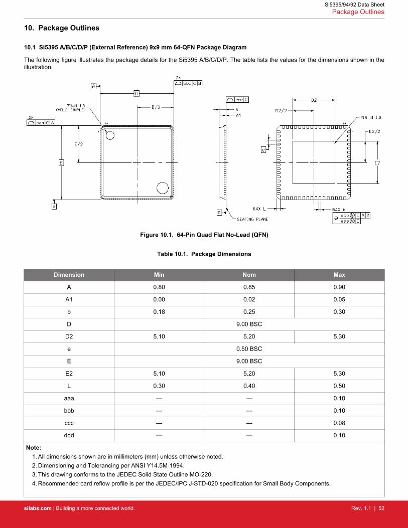
10. Package Outlines
10.1 Si5395 A/B/C/D/P (External Reference) 9x9 mm 64-QFN Package Diagram
The following figure illustrates the package details for the Si5395 A/B/C/D/P. The table lists the values for the dimensions shown in theillustration.
Figure 10.1. 64-Pin Quad Flat No-Lead (QFN)
Table 10.1. Package Dimensions
Dimension Min Nom Max
A 0.80 0.85 0.90
A1 0.00 0.02 0.05
b 0.18 0.25 0.30
D 9.00 BSC
D2 5.10 5.20 5.30
e 0.50 BSC
E 9.00 BSC
E2 5.10 5.20 5.30
L 0.30 0.40 0.50
aaa — — 0.10
bbb — — 0.10
ccc — — 0.08
ddd — — 0.10
Note:1. All dimensions shown are in millimeters (mm) unless otherwise noted.2. Dimensioning and Tolerancing per ANSI Y14.5M-1994.3. This drawing conforms to the JEDEC Solid State Outline MO-220.4. Recommended card reflow profile is per the JEDEC/IPC J-STD-020 specification for Small Body Components.
Si5395/94/92 Data SheetPackage Outlines
silabs.com | Building a more connected world. Rev. 1.1 | 52

10.2 Si5395 J/K/L/M/E (Internal Reference) 9x9 mm 64-LGA Package Diagram
The following figure illustrates the package details for the Si5395 J/K/L/M/E. The table lists the values for the dimensions shown in theillustration.
Figure 10.2. 64-Pin LGA
Table 10.2. Package Dimensions
Dimension Min Nom Max
A 0.9 1 1.1
A1 0.26 REF
A2 0.70 REF
b 0.2 0.25 0.3
b1 0.8 0.85 0.9
D 9 BSC
E 9 BSC
e 0.5 BSC
e1 1.0 BSC
L 0.315 0.365 0.415
L1 0.080 REF
aaa 0.1
bbb 0.2
ccc 0.1
ddd 0.08
Note:1. All dimensions shown are in millimeters (mm) unless otherwise noted.2. Dimensioning and Tolerancing per ANSI Y14.5M-1994.3. This drawing conforms to the JEDEC Solid State Outline MO-220.4. Recommended card reflow profile is per the JEDEC/IPC J-STD-020 specification for Small Body Components.
Si5395/94/92 Data SheetPackage Outlines
silabs.com | Building a more connected world. Rev. 1.1 | 53

10.3 Si5394 and Si5392 A/B/C/D/P (External Reference) 7x7 mm 44-QFN Package Diagram
The following figure illustrates the package details for the Si5394 and Si5392. The table lists the values for the dimensions shown in theillustration.
Figure 10.3. 44-Pin Quad Flat No-Lead (QFN)
Table 10.3. Package Dimensions
Dimension Min Nom Max
A 0.80 0.85 0.90
A1 0.00 0.02 0.05
b 0.18 0.25 0.30
D 7.00 BSC
D2 5.10 5.20 5.30
e 0.50 BSC
E 7.00 BSC
E2 5.10 5.20 5.30
L 0.30 0.40 0.50
aaa — — 0.10
bbb — — 0.10
ccc — — 0.08
ddd — — 0.10
Note:1. All dimensions shown are in millimeters (mm) unless otherwise noted.2. Dimensioning and Tolerancing per ANSI Y14.5M-1994.3. This drawing conforms to the JEDEC Solid State Outline MO-220.4. Recommended card reflow profile is per the JEDEC/IPC J-STD-020 specification for Small Body Components.
Si5395/94/92 Data SheetPackage Outlines
silabs.com | Building a more connected world. Rev. 1.1 | 54

10.4 Si5394 and Si5392 J/K/L/M/E (Internal Reference) 7x7 mm 44-LGA Package Diagram
The following figure illustrates the package details for the Si5394J and Si5392J. The table lists the values for the dimensions shown inthe illustration.
Figure 10.4. 44-Pin LGA
Table 10.4. Package Dimensions
Dimension Min Nom Max
A — — 1.10
A1 0.26 REF
A2 0.7 REF
b 0.20 0.25 0.30
D 7.00 BSC
D2 5.10 5.20 5.30
e 0.50 BSC
E 7.00 BSC
E2 5.10 5.20 5.30
L 0.35 0.40 0.45
aaa — — 0.10
bbb — — 0.20
ccc — — —
ddd — — 0.08
eee — — —
Note:1. All dimensions shown are in millimeters (mm) unless otherwise noted.2. Dimensioning and Tolerancing per ANSI Y14.5M-1994.3. This drawing conforms to the JEDEC Solid State Outline MO-220.4. Recommended card reflow profile is per the JEDEC/IPC J-STD-020 specification for Small Body Components.
Si5395/94/92 Data SheetPackage Outlines
silabs.com | Building a more connected world. Rev. 1.1 | 55

11. PCB Land Pattern
The following figure illustrates the PCB land pattern details for the devices. The table lists the values for the dimensions shown in theillustration.
Si5395 Si5394 and Si5392
Figure 11.1. PCB Land Pattern
Si5395/94/92 Data SheetPCB Land Pattern
silabs.com | Building a more connected world. Rev. 1.1 | 56
Table 11.1. PCB Land Pattern Dimensions
Dimension Si5395 (Max) Si5394/92 (Max)
C1 8.90 6.90
C2 8.90 6.90
E 0.50 0.50
X1 0.30 0.30
Y1 0.85 0.85
X2 5.30 5.30
Y2 5.30 5.30
Notes:
General1. All dimensions shown are in millimeters (mm) unless otherwise noted.2. This Land Pattern Design is based on the IPC-7351 guidelines.3. All dimensions shown are at Maximum Material Condition (MMC). Least Material Condition is calculated based on a fabrication
Allowance of 0.05 mm.
Solder Mask Design1. All metal pads are to be non-solder mask defined (NSMD). Clearance between the solder mask and the metal pad is to be 60 µm
minimum, all the way around the pad.
Stencil Design1. A stainless steel, laser-cut and electropolished stencil with trapezoidal walls should be used to assure good solder paste release.2. The stencil thickness should be 0.125 mm (5 mils).3. The ratio of stencil aperture to land pad size should be 1:1 for all perimeter pads.4. While the same land pattern design can be used for both QFN and LGA package types, the stencil design will need to match the
respective ground pads as shown in the Package outline.
Card Assembly1. A No-Clean, Type-3 solder paste is recommended.2. The recommended card reflow profile is per the JEDEC/IPC J-STD-020 specification for Small Body Components.
Si5395/94/92 Data SheetPCB Land Pattern
silabs.com | Building a more connected world. Rev. 1.1 | 57

12. Top Marking
Figure 12.1. Top Marking
Table 12.1. Top Marking Explanation
Line Characters Description
1 Si539fg-
Base part number and Device Grade for Any-frequency, Any-output, JitterCleaning Clock (single PLL):
f = 5: 12-output Si5395: 64-QFN
f = 4: 4-output Si5394: 44-QFN
f = 2: 2-output Si5392: 44-QFN
g = Device Grade (A/B/C/D/P/J/K/L/M/E). See 3. Ordering Guide for more infor-mation.
– = Dash character.
2 Rxxxxx-GM
R = Product revision. (Refer to 3. Ordering Guide for latest revision).
xxxxx = Customer specific NVM sequence number. Optional NVM code as-signed for custom, factory pre-programmed devices.
Characters are not included for standard, factory default configured devices.See 3. Ordering Guide for more information.
-GM = Package (QFN) and temperature range (–40 to +85 °C)
3 YYWWTTTTTTYYWW = Characters correspond to the year (YY) and work week (WW) ofpackage assembly.
TTTTTT = Manufacturing trace code.
4Circle w/ 1.6 mm (64-QFN) or 1.4
mm (44-QFN) diameter Pin 1 indicator; left-justified
CC CC = TW = Taiwan; Country of Origin (ISO Abbreviation)
Si5395/94/92 Data SheetTop Marking
silabs.com | Building a more connected world. Rev. 1.1 | 58

13. Revision History
Revision 1.1
June, 2019• Added Integrated reference options J/K/L/M/E.
Revision 1.0
April, 2019• Updated Figure 4.3. Crystal Resonator and External Reference Clock Connection Options• Updated section 4.9.2 Grade P section to support up to 3 time domains for Si5395, 2 domains for Si5394 and 1 domain for Si5392
(previous version only specified 2 domains for Si5395)• Table 5.2 DC Characteristics
• Core supply current IDD/IDDA limits clarified for each device• Output Buffer supply conditions clarified• Total power dissipation numbers updated• Updated test configuration diagrams
• Table 5.3 Input clock specifications• Updated Input voltage section of "LVCMOS / Pulsed CMOS DC-Coupled Input Buffer" to include standard CMOS
• Table 5.5 Differential Clock Output Specifications• Clarified duty cycle specs for when MultiSynth is used/not used• Increased max Rise and Fall times from 150ps to 200ps based on final characterization
• Table 5.6. LVCMOS Clock Output Specifications• Updated Min and Max limits for duty cycle• Updated test configuration diagrams
• Table 5.8. Performance Characteristics• Updated Initial startup time for P-grade devices• Updated P-grade jitter numbers to include more domains and finalize test conditions
• Updated Table 5.10. SPI Timing Specifications (4-Wire) table and timing diagram• Updated Table 5.11. SPI Timing Specifications (3-Wire)• Changed NC/XA, NC/XB, NC/X1, NC/X2 to XA, XB, X1, X2 respectively since integrated crystal devices are getting their own data
sheet
Revision 0.96
June, 2018• Preliminary data sheet.
Si5395/94/92 Data SheetRevision History
silabs.com | Building a more connected world. Rev. 1.1 | 59
ClockBuilder ProOne-click access to Timing tools, documentation, software, source code libraries & more. Available for Windows and iOS (CBGo only).
www.silabs.com/CBPro
Timing Portfoliowww.silabs.com/timing
SW/HWwww.silabs.com/CBPro
Qualitywww.silabs.com/quality
Support and Communitycommunity.silabs.com
http://www.silabs.com
Silicon Laboratories Inc.400 West Cesar ChavezAustin, TX 78701USA
DisclaimerSilicon Labs intends to provide customers with the latest, accurate, and in-depth documentation of all peripherals and modules available for system and software implementers using or intending to use the Silicon Labs products. Characterization data, available modules and peripherals, memory sizes and memory addresses refer to each specific device, and "Typical" parameters provided can and do vary in different applications. Application examples described herein are for illustrative purposes only. Silicon Labs reserves the right to make changes without further notice to the product information, specifications, and descriptions herein, and does not give warranties as to the accuracy or completeness of the included information. Without prior notification, Silicon Labs may update product firmware during the manufacturing process for security or reliability reasons. Such changes will not alter the specifications or the performance of the product. Silicon Labs shall have no liability for the consequences of use of the information supplied in this document. This document does not imply or expressly grant any license to design or fabricate any integrated circuits. The products are not designed or authorized to be used within any FDA Class III devices, applications for which FDA premarket approval is required or Life Support Systems without the specific written consent of Silicon Labs. A "Life Support System" is any product or system intended to support or sustain life and/or health, which, if it fails, can be reasonably expected to result in significant personal injury or death. Silicon Labs products are not designed or authorized for military applications. Silicon Labs products shall under no circumstances be used in weapons of mass destruction including (but not limited to) nuclear, biological or chemical weapons, or missiles capable of delivering such weapons. Silicon Labs disclaims all express and implied warranties and shall not be responsible or liable for any injuries or damages related to use of a Silicon Labs product in such unauthorized applications.
Trademark InformationSilicon Laboratories Inc.® , Silicon Laboratories®, Silicon Labs®, SiLabs® and the Silicon Labs logo®, Bluegiga®, Bluegiga Logo®, Clockbuilder®, CMEMS®, DSPLL®, EFM®, EFM32®, EFR, Ember®, Energy Micro, Energy Micro logo and combinations thereof, "the world’s most energy friendly microcontrollers", Ember®, EZLink®, EZRadio®, EZRadioPRO®, Gecko®, Gecko OS, Gecko OS Studio, ISOmodem®, Precision32®, ProSLIC®, Simplicity Studio®, SiPHY®, Telegesis, the Telegesis Logo®, USBXpress® , Zentri, the Zentri logo and Zentri DMS, Z-Wave®, and others are trademarks or registered trademarks of Silicon Labs. ARM, CORTEX, Cortex-M3 and THUMB are trademarks or registered trademarks of ARM Holdings. Keil is a registered trademark of ARM Limited. Wi-Fi is a registered trademark of the Wi-Fi Alliance. All other products or brand names mentioned herein are trademarks of their respective holders.