siddharth institute of engineering & technology (autonomous)
TRANSCRIPT
ELECTRONIC DEVICES LAB
Department of ECE 1
SIDDHARTH INSTITUTE OF ENGINEERING & TECHNOLOGY
(AUTONOMOUS) (Approved by AICTE, New Delhi & Affiliated to JNTUA, Ananthapuramu)
(Accredited by NBA & Accredited by NAAC with ‘A’ Grade) Siddharth Nagar, Narayanavanam Road, PUTTUR-517 583
Department of Electronics and Communication Engineering
18EC0404 - ELECTRONIC DEVICES LABORATORY MANUAL
PREPARED BY VERIFIED BY
1. M.AFSAR ALI Dr.P.RATNA KAMALA, Ph.D
Professor Professor & HOD
2. S.B.RANJANI
Assistant Professor

ELECTRONIC DEVICES LAB
Department of ECE 2
Department of Electronics and Communication Engineering
Vision
To emerge as a premier department in Electronics and Communication
Engineering Education, producing creative technocrats who can address the
challenges of the new century for the benefit of society.
Mission
To impart professional education with human values to transform students to
be competent and committed electronics and communication engineers,
researchers and academicians capable of providing solutions to the global
challenges.
Preface
This laboratory manual is prepared by the department of Electronics and Communication
Engineering for Electronic Devices (18EC0404) Lab. This lab manual can be used as instructional
book for students, staff and instructors to assist in performing and understanding the experiments.

ELECTRONIC DEVICES LAB
Department of ECE 3
Course objective:
The objectives of this course is to
• Make the student understand the working of various Semiconductor devices and plot their
characteristics.
• Obtain the frequency response characteristics of BJT and FET amplifiers.
Course Outcomes:
Upon completion of this course, the student will be able to:
• Know various semiconductor devices and their use in Real time applications.
• Find the Frequency response characteristics of BJT and FET amplifiers and determine
bandwidth.

ELECTRONIC DEVICES LAB
Department of ECE 4
SYLLABUS
List of Experiments (Minimum of TEN experiments to be completed)
CYCLE-I
1. Forward and Reverse bias characteristics of P-N Junction diode
2. Zener diode characteristics
3. Diode clippers
4. Diode clampers
5. Half Wave Rectifier with and without filter
6. Full Wave Rectifier with and without filter
CYCLE –II
7. Input and Output characteristics of Transistor in CB Configuration
8. Input and Output characteristics of Transistor in CE Configuration
9. Drain and Transfer Characteristics of n-channel JFET
10. Frequency response of CE Amplifier
11. Frequency response of CC Amplifier
12. Frequency response of Common Source FET Amplifier
ELECTRONIC DEVICES LAB
Department of ECE 5
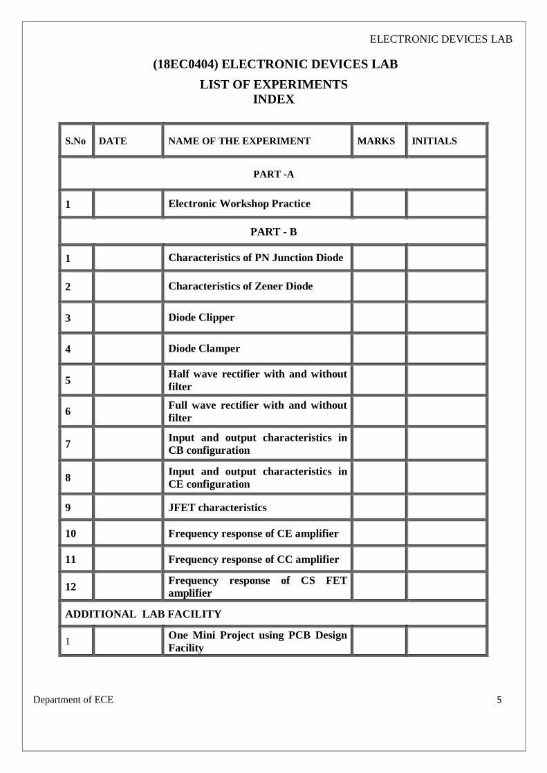
(18EC0404) ELECTRONIC DEVICES LAB
LIST OF EXPERIMENTS
INDEX
S.No DATE NAME OF THE EXPERIMENT MARKS INITIALS
PART -A
1 Electronic Workshop Practice
PART - B
1 Characteristics of PN Junction Diode
2 Characteristics of Zener Diode
3 Diode Clipper
4 Diode Clamper
5 Half wave rectifier with and without
filter
6 Full wave rectifier with and without
filter
7 Input and output characteristics in
CB configuration
8 Input and output characteristics in
CE configuration
9 JFET characteristics
10 Frequency response of CE amplifier
11 Frequency response of CC amplifier
12 Frequency response of CS FET
amplifier
ADDITIONAL LAB FACILITY
1 One Mini Project using PCB Design
Facility

ELECTRONIC DEVICES LAB
Department of ECE 6
PART A: Electronic Workshop Practice
1. Identification, Specifications and Testing of passive & active components
2. Study the working of the electronic equipment used in the lab.
Aim:
To study the identification and specification of R, L, and C components, Potentiometers, Coils, Gang
Condensers, Relays, Bread Boards and also to understand the working of the electronic equipments
like Cathode Ray oscilloscope(CRO), Function Generator and Regulated Power Supply (RPS).
Apparatus Required:
S.NO COMPONENTS QUANTITY
1 Resistor 1
2 Capacitor 1
3 Inductor 1
4 Potentiometer 1
5 Coils 1
6 Gang Condenser 1
7 Relay 1
8 Bread board 1
9 CRO 1
10 Function Generator 1
11 Regulated Power Supply 1
Theory:
1. RESISTOR:
Resistor is an electronic component whose function is to limit the flow of current in an electric
circuit. It is measured in units called ohms. The symbol for ohm is (omega).
Without resistors voltage would be too great for individual components to handle and would result in
overloading or destruction.
Identification:
“Color coding” is used in electronics to identify between different components. Electronic
components like resistors are very small in size and it is difficult to print its value directly on to the
component surface. Hence a standard was formed in 1920 by then Radio Manufacturers Association (now
part of EIA – Electronic Industries Alliance) to identify values and ratings of electronic components by
printing color codes on them.
Specification:
In the case of resistors, a specific resistance value is represented using ohms, For example a 100
ohms resistor or a 1 kilo ohms resistor with 5% tolerance. The resistors are represented by using its symbol
in the circuit.
a. Fixed resistor
b. Potentiometer
c. Typical resistor wattage sizes are 1/8, 1/4, 1/2, 1, 2, 5, 10 and 20 (w) units, depending on thickness of
leads Wattage
d. variable Resistor

ELECTRONIC DEVICES LAB
Department of ECE 7
e. Potentiometer
Typical resistor wattage sizes are 1/8, 1/4, 1/2, 1, 2, 5, 10 and 20 (w) units, depending on thickness of
leads Wattage of resistors can be decided. The various types of resistors are carbon resistor, thin film
resistor, wire wound resistor and rheostat.
Testing:
1. Connect the measuring probes into the socket of the Digital Multimeter.
2. Switch on the Multimeter and set the knob to ohms position.
3. Now measure the resistance by placing the testing probes on either side of the resistor.
4. The value of the resistance in ohms is noted and verified using color coding
5. If no value is displayed, see the resistor for any burnt shades or damages.

ELECTRONIC DEVICES LAB
Department of ECE 8
2. CAPACITOR
The Capacitor, sometimes referred to as a Condenser, is a simple passive device that is used to
store electricity. The capacitor is a component which has the ability or capacity to store energy in the
form of an electrical charge producing a potential difference (Static Voltage) across its plates, much like
a small rechargeable battery.
Identification:
Capacitors are identified using the value written on the body. There are some capacitors which are
identified using color codes. A capacitor is said to be “Fully Charged” when the voltage across its plates
equals the supply voltage. The symbol for electrical charge is Q and its unit is the Coulomb.
Specification:
Electrolytic capacitors are polarized. They have a +ve and a -ve terminal. Capacitance is measured in
Farads, which is a very large unit so micro-Farad (uF), Nano-Farad (nF) and Pico-Farad (pF) are
generally used. Capacitive reactance is the opposition to current flow in AC circuits. In AC capacitive
circuits the voltage “lags” the current by 90o.
To specify the value of the ceramic capacitor we use the code table shown below
Picofarad
(pF)
Nanofarad
(nF)
Microfarad
(uF) Code
Picofarad
(pF)
Nanofarad
(nF)
Microfarad
(uF) Code
10 0.01 0.00001 100 4700 4.7 0.0047 472
15 0.015 0.000015 150 5000 5.0 0.005 502
22 0.022 0.000022 220 5600 5.6 0.0056 562
33 0.033 0.000033 330 6800 6.8 0.0068 682
47 0.047 0.000047 470 10000 10 0.01 103
100 0.1 0.0001 101 15000 15 0.015 153
120 0.12 0.00012 121 22000 22 0.022 223
130 0.13 0.00013 131 33000 33 0.033 333
150 0.15 0.00015 151 47000 47 0.047 473
180 0.18 0.00018 181 68000 68 0.068 683

ELECTRONIC DEVICES LAB
Department of ECE 9
220 0.22 0.00022 221 100000 100 0.1 104
330 0.33 0.00033 331 150000 150 0.15 154
470 0.47 0.00047 471 200000 200 0.2 254
560 0.56 0.00056 561 220000 220 0.22 224
680 0.68 0.00068 681 330000 330 0.33 334
750 0.75 0.00075 751 470000 470 0.47 474
820 0.82 0.00082 821 680000 680 0.68 684
1000 1.0 0.001 102 1000000 1000 1.0 105
1500 1.5 0.0015 152 1500000 1500 1.5 155
2000 2.0 0.002 202 2000000 2000 2.0 205
2200 2.2 0.0022 222 2200000 2200 2.2 225
3300 3.3 0.0033 332 3300000 3300 3.3 335
Testing:
1. Checking this capacitor with a capacitance meter is straight forward. On these capacitors, the positive
lead is marked. Attach the positive (red) lead from the meter to that and the negative (black) to the
opposite. This capacitor shows 1038μF, clearly within its tolerance.
2. In this example, the capacitor will be charged with a 9V DC battery for a few seconds. After the
charge is finished, disconnect the battery from the capacitor. Use the multi-meter and read the voltage
on the capacitor leads. The voltage should read near 9 volts. The voltage will discharge rapidly to 0V
because the capacitor is discharging through the multi-meter. If the capacitor will not retain that
voltage, it is defective and should be replaced
3. INDUCTOR
A current through a conductor produces a magnetic field surround it. The strength of this field
depends upon the value of current passing through the conductor. The direction of the magnetic field is
found using the right hand grip rule, which shown. The flux pattern for this magnetic field would be number
of concentric circle perpendicular to the detection of current. Now if we wound the conductor in form of a
coil or solenoid, it can be assumed that there will be concentric circular flux lines for each individual turn of
the coil as shown.
But it is not possible practically, as if concentric circular flux lines for each individual turn exist,
they will intersect each other. However, since lines of flux cannot intersect, the flux lines for individual turn
will distort to form complete flux loops around the whole coil as shown. This flux pattern of a current
carrying coil is similar to a flux pattern of a bar magnet as shown.
Now if the current through the coil is changed, the magnetic flux produced by it will also be changed
at same rate. As the flux is already surrounds the coil, this changing flux obviously links the coil. Now

ELECTRONIC DEVICES LAB
Department of ECE 10
according to Faraday‟s law of electromagnetic induction, if changing flux links with a coil, there would be
an induced emf in it. Again as per Lenz‟s law this induced emf opposes every cause of producing it. Hence,
the induced emf is in opposite of the applied voltage across the coil.
Unit of Inductance
Which we derived at equation, Where, L is known is the self-induction of the circuit. In the above equation
of inductance, if e = 1 Volt and (di / dt) is one ampere per second, then L = 1 and its unit is Henry. That
means, if a circuit, produces emf of 1 Volt, due to the rate of change of current through it, one ampere per
second then the circuit is said to have one henry self-inductance. This Henry is unit of inductance
Potentiometers:
A potentiometer, informally a pot, is a three-terminal resistor with a sliding or rotating contact that
forms an adjustable voltage divider.[1]
If only two terminals are used, one end and the wiper, it acts as a
variable resistor or rheostat.
The measuring instrument called a potentiometer is essentially a voltage divider used for measuring
electric potential (voltage); the component is an implementation of the same principle, hence its name.
Potentiometers are commonly used to control electrical devices such as volume controls on audio
equipment. Potentiometers operated by a mechanism can be used as position transducers, for example, in a
joystick. Potentiometers are rarely used to directly control significant power (more than a watt), since the
power dissipated in the potentiometer would be comparable to the power in the controlled load.
Coils:
An electromagnetic coil is an electrical conductor such as a wire in the shape of a coil, spiral or
helix. Electromagnetic coils are used in electrical engineering, in applications where electric currents
interact with magnetic fields, in devices such as inductors, electromagnets, transformers, and sensor coils.
Either an electric current is passed through the wire of the coil to generate a magnetic field, or conversely an
external time-varying magnetic field through the interior of the coil generates an EMF (voltage) in the
conductor.
Coils can be classified by the frequency of the current they are designed to operate with:
Direct current or DC coils or electromagnets operate with a steady direct current in their
windings
Audio-frequency or AF coils, inductors or transformers operate with alternating currents in
the audio frequency range, less than 20 kHz
Radio-frequency or RF coils, inductors or transformers operate with alternating currents in
the radio frequency range, above 20 kHz

ELECTRONIC DEVICES LAB
Department of ECE 11
Gang Condenser:
A gang condenser is a a variable capacitor. A variable capacitor is constructed in such manner that its
value of capacitance can be varied. A typical variable capacitor (adjustable capacitor) is the rotor-stator type.
It consists of two sets of metal plates arranged so that the rotor plates move between the stator plates. Air is
the dielectric. As the position of the rotor is changed, the capacitance value is likewise changed. This type of
capacitor is used for tuning most radio receivers.
Relays:
A relay is an electrically operated switch. Many relays use an electromagnet to mechanically operate
a switch, but other operating principles are also used, such as solid-state relays. Relays are used where it is
necessary to control a circuit by a low-power signal (with complete electrical isolation between control and
controlled circuits), or where several circuits must be controlled by one signal. The first relays were used in
long distance telegraph circuits as amplifiers: they repeated the signal coming in from one circuit and re-
transmitted it on another circuit. Relays were used extensively in telephone exchanges and early computers
to perform logical operations.
Bread Board:
A breadboard is a construction base for prototyping of electronics. Originally it was literally a bread
board, a polished piece of wood used for slicing bread. In the 1970s the solder less breadboard (AKA plug
board, a terminal array board) became available and nowadays the term "breadboard" is commonly used to
refer to these. "Breadboard" is also a synonym for "prototype". Because the solder less breadboard does not
require soldering, it is reusable. This makes it easy to use for creating temporary prototypes and

ELECTRONIC DEVICES LAB
Department of ECE 12
experimenting with circuit design. For this reason, solder less breadboards are also extremely popular with
students and in technological education. Older breadboard types did not have this property. A strip board
(Vero board) and similar prototyping printed circuit boards, which are used to build semi-permanent
soldered prototypes or one-offs, cannot easily be reused.
CATHODE RAY OSCILLOSCOPE (CRO):
Display and general external appearance
An oscilloscope is an electronic measuring device which provides a two- dimensional visual representation
of a signal. Because the oscilloscope allows the user to see the signal(s), their characteristics can be easily
measured and observed. The oscilloscope displays a graph of voltage (on the vertical axis) versus time (on
the horizontal axis). Most electrical circuits can be easily connected to the oscilloscope typically with
probes. CRO (for cathode-ray oscilloscope), or DSO (for the more modern digital storage oscilloscope), is a
type of electronic test instrument that allows observation of constantly varying signal voltages, usually as a
two-dimensional graph of one or more electrical potential differences using the vertical or 'Y' axis, plotted
as a function of time (horizontal or 'x'axis).
Measuring voltage and time period:
The trace on an oscilloscope screen is a graph of voltage against time. The shape of this graph is determined
by the nature of the input signal. In addition to the properties labeled on the graph, there is frequency which
is the number of cycles per second. The diagram shows a sine wave but these properties apply to any signal
with a constant shape
Properties of trace
Amplitude is the maximum voltage reached by the signal. It is measured in volts.
Peak voltage is another name for amplitude.
ELECTRONIC DEVICES LAB
Department of ECE 13
Peak-peak voltage is twice the peak voltage (amplitude). When reading an oscilloscope trace
it is usual to measure peak-peak voltage.
Time period is the time taken for the signal to complete one cycle.
It is measured in seconds (s), but time periods tend to be short so milliseconds (ms) and microseconds (µs) are often used. 1ms = 0.001s and 1µs = 0.000001s.
Frequency is the number of cycles per second. It is measured in hertz (Hz), but frequencies
tend to be high so kilohertz (kHz) and megahertz (MHz) are often used. 1kHz = 1000Hz and
1MHz =1000000Hz
Time period= 1 / frequency
A) Voltage: Voltage is shown on the vertical y-axis and the scale is determined by the Y
AMPLIFIER (VOLTS/CM) control. Usually peak-peak voltage is measured because it can be
read correctly even if the position of 0V is not known. The amplitude is half the peak-peak
voltage.
Voltage = distance in cm × volts/cm
B) Time period: Time is shown on the horizontal x-axis and the scale is determined by the
TIMEBASE (TIME/CM) control. The time period (often just called period) is the time for one
cycle of the signal. The frequency is the number of cycles per second, frequency = 1/time period.
Time = distance in cm × time/cm
Applications of CRO:
General-purpose instruments are used for maintenance of electronic equipment and laboratory work.
Special-purpose oscilloscopes may be used for such purposes as analyzing an automotive ignition system, or to display the waveform of the heartbeat as an electrocardiogram.
Some computer sound software allows the sound being listened to be displayed on the
screen as by an oscilloscope.
FUNCTION GENERATOR:
A function generator is usually a piece of electronic test equipment or software used to generate
different types of electrical waveforms over a wide range of frequencies. Some of the most
common waveforms produced by the function generator are the sine, square, triangular and
sawtooth shapes. These waveforms can be either repetitive or single-shot (which requires an
internal or external trigger source). Integrated circuits used to generate waveforms may also be
described as function generator ICs. The function generator is used to generate a wide range of
alternating-current (AC) signals. A typical function generator can provide frequencies up to 20
MHz. RF generators for higher frequencies are not function generators in the strict sense since they
typically produce pure or modulated sine signals only.
Typical specifications for a general-purpose function generator are Produces sine, square, triangular, sawtooth (ramp), and pulse output. Arbitrary waveform generators can produce waves of any shape. It
can generate a wide range of frequencies.
Frequency Selection:
These controls are used to select the operating frequency of the function generator. This group
consists of the frequency control knob and the eight frequency multiplier selection buttons.

ELECTRONIC DEVICES LAB
Department of ECE 14
For example,
To set the function generator to an operating frequency of 2000 Hz (2 kHz):
• Rotate the frequency control knob to2.
• Select the 1 kHz frequency multiplier button.
With the result that: 2.0 * 1 kHz = 2.0 kHz.
To set the function generator to an operating frequency of 5.5 kHz:
• Rotate the frequency control knob to0.55.
• Select the 10 kHz frequency multiplier button.
With the result that: 0.55 * 10 kHz = 5.5 kHz.
Generate a waveform of 5.5 KHz.
To set the function generator to an operating frequency of 2000 Hz (2 kHz):
• Rotate the frequency control knob to2.
• Select the 1 kHz frequency multiplier button. With the result that: 2.0 * 1 kHz = 2.0kHz.
To set the function generator to an operating frequency of 5.5 kHz:
• Rotate the frequency control knob to0.55.
• Select the 10 kHz frequency multiplier button.
With the result that: 0.55 * 10 kHz = 5.5 kHz.
REGULATED POWER SUPPLY (RPS):
There are many types of power supply. Most are designed to convert high voltage AC mains
electricity to a suitable low voltage supply for electronic circuits and other devices. A power supply can by
broken down into a series of blocks, each of which performs a particular function. For example, a 5V
regulated supply:
Figure1: Block Diagram of Regulated Power Supply
Each of the blocks is described in more detail below:
Transformer: Steps down high voltage AC mains to low voltage AC.
Rectifier: Converts AC to DC, but the DC output is varying.
Smoothing: Smooths the DC from varying greatly to a small ripple.
Regulator: Eliminates ripple by setting DC output to a fixed voltage.
Dual Supplies:
Some electronic circuits require a power supply with positive and negative outputs as well as zero volts
(0V). This is called a 'dual supply' because it is like two ordinary supplies connected together as shown in the
diagram.
Dual supplies have three outputs, for example a ±9V supply has +9V, 0V and -9V outputs.

ELECTRONIC DEVICES LAB
Department of ECE 15
Result:
Thus, the various Apparatus used in electronics lab were studied and practiced.
ELECTRONIC DEVICES LAB
Department of ECE 16
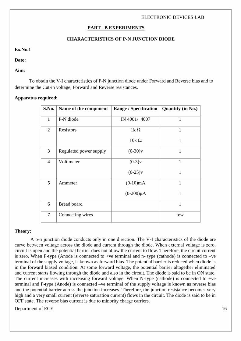
PART –B EXPERIMENTS
CHARACTERISTICS OF P-N JUNCTION DIODE
Ex.No.1
Date:
Aim:
To obtain the V-I characteristics of P-N junction diode under Forward and Reverse bias and to
determine the Cut-in voltage, Forward and Reverse resistances.
Apparatus required:
S.No. Name of the component Range / Specification Quantity (in No.)
1 P-N diode IN 4001/ 4007 1
2 Resistors 1k Ω
10k Ω
1
1
3 Regulated power supply (0-30)v 1
4 Volt meter (0-3)v
(0-25)v
1
1
5 Ammeter (0-10)mA
(0-200)μA
1
1
6 Bread board 1
7 Connecting wires few
Theory:
A p-n junction diode conducts only in one direction. The V-I characteristics of the diode are
curve between voltage across the diode and current through the diode. When external voltage is zero,
circuit is open and the potential barrier does not allow the current to flow. Therefore, the circuit current
is zero. When P-type (Anode is connected to +ve terminal and n- type (cathode) is connected to –ve
terminal of the supply voltage, is known as forward bias. The potential barrier is reduced when diode is
in the forward biased condition. At some forward voltage, the potential barrier altogether eliminated
and current starts flowing through the diode and also in the circuit. The diode is said to be in ON state.
The current increases with increasing forward voltage. When N-type (cathode) is connected to +ve
terminal and P-type (Anode) is connected –ve terminal of the supply voltage is known as reverse bias
and the potential barrier across the junction increases. Therefore, the junction resistance becomes very
high and a very small current (reverse saturation current) flows in the circuit. The diode is said to be in
OFF state. The reverse bias current is due to minority charge carriers.

ELECTRONIC DEVICES LAB
Department of ECE 17
Fig.1

ELECTRONIC DEVICES LAB
Department of ECE 18
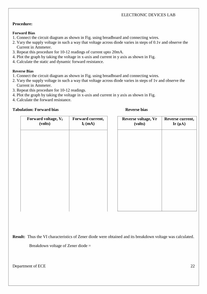
Tabulation: (Forward bias)
Forward voltage, Vf
(volts)
Forward current, If
(mA)
Tabulation: (Reverse bias)
Reverse voltage, Vr
(volts)
Reverse current, Ir
(μA)

ELECTRONIC DEVICES LAB
Department of ECE 19
Procedure:
Forward Bias
1. Connect the circuit diagram as shown in Fig.1(a) using breadboard and connecting wires.
2. Vary the supply voltage in such a way that voltage across diode varies in steps of 0.1v and observe the
Current in Ammeter.
3. Repeat this procedure for 10-12 readings of current upto 20mA.
4. Plot the graph by taking the voltage in x-axis and current in y axis as shown in Fig.1(c).
4. Calculate the static and dynamic forward resistance.
Reverse Bias
1. Connect the circuit diagram as shown in Fig.1(b) using breadboard and connecting wires.
2. Vary the supply voltage in such a way that voltage across diode varies in steps of 1v and observe the
Current in Ammeter.
3. Repeat this procedure for 10-12 readings.
4. Plot the graph by taking the voltage in x-axis and current in y axis as shown in Fig.1(c).
4. Calculate the forward resistance.
Calculations:
Cut-in Voltage, Vᵧ =
Forward Static resistance = Vf/If=
Forward Dynamic resistance = ΔVf/ΔIf =
Reverse resistance = Vr/Ir =
Result:
Thus the V-I characteristics of P-N junction diode were obtained and the forward and reverse
resistance were calculated.
Cut-in Voltage, Vᵧ =
Forward Static resistance =
Forward Dynamic resistance =
Reverse resistance =

ELECTRONIC DEVICES LAB
Department of ECE 20
CHARACTERISTICS OF ZENER DIODE
Ex.No.2
Date:
Aim: To plot the V-I characteristics of Zener diode under forward and reverse bias and to find the
Breakdown voltage of it.
Apparatus required:
S.No. Name of the
component
Range /
Specification
Quantity (in No.)
1 Zener diode FZ 5.1v 1
2 Resistors 1k Ω
10k Ω
1
1
3 Regulated power supply (0-30)V 1
4 Voltmeter (0-3)V
(0-25)V
1
1
5 Ammeter (0-10)mA
(0-100)mA
1
1
6 Bread board 1
7 Connecting wires few
Theory:
A Zener diode is a type of diode that permits current not only in the forward direction like a
normal diode, but also in the reverse direction if the voltage is larger than the breakdown voltage
known as "Zener knee voltage" or "Zener voltage". The device was named after Clarence Zener, who
discovered this electrical property. A conventional solid-state diode will not allow significant current if
it is reverse-biased below its reverse breakdown voltage. When the reverse bias breakdown voltage is
exceeded, a conventional diode is subject to high current due to avalanche breakdown. Unless this
current is limited by circuitry, the diode will be permanently damaged due to overheating. In case of
large forward bias (current in the direction of the arrow), the diode exhibits a voltage drop due to its
junction built-in voltage and internal resistance. The amount of the voltage drop depends on the
semiconductor material and the doping concentrations.
A Zener diode exhibits almost the same properties, except the device is specially designed so as
to have a greatly reduced breakdown voltage, the so-called Zener voltage. The Zener diode‟s
breakdown characteristics are determined by the doping process. Low voltage Zeners (>5V), operate in
the Zener breakdown range. Those designed to operate <5 V operate mostly in avalanche breakdown
range. Zener diodes are available with voltage breakdowns of 1.8 V to 200 V.

ELECTRONIC DEVICES LAB
Department of ECE 21
ELECTRONIC DEVICES LAB
Department of ECE 22
Procedure:
Forward Bias
1. Connect the circuit diagram as shown in Fig. using breadboard and connecting wires.
2. Vary the supply voltage in such a way that voltage across diode varies in steps of 0.1v and observe the
Current in Ammeter.
3. Repeat this procedure for 10-12 readings of current upto 20mA.
4. Plot the graph by taking the voltage in x-axis and current in y axis as shown in Fig.
4. Calculate the static and dynamic forward resistance.
Reverse Bias
1. Connect the circuit diagram as shown in Fig. using breadboard and connecting wires.
2. Vary the supply voltage in such a way that voltage across diode varies in steps of 1v and observe the
Current in Ammeter.
3. Repeat this procedure for 10-12 readings.
4. Plot the graph by taking the voltage in x-axis and current in y axis as shown in Fig.
4. Calculate the forward resistance.
Tabulation: Forward bias Reverse bias
Result: Thus the VI characteristics of Zener diode were obtained and its breakdown voltage was calculated.
Breakdown voltage of Zener diode =
Forward voltage, Vf
(volts)
Forward current,
If (mA)
Reverse voltage, Vr
(volts)
Reverse current,
Ir (μA)

ELECTRONIC DEVICES LAB
Department of ECE 23
DIODE CLIPPERS
Ex.No.3
Date:
Aim: To study the clipping circuits for different reference voltages and to verify the responses.
Apparatus required:
S.No. Name of the
component
Range /
Specification
Quantity (in No.)
1 PN Junction Diode 1N4001 1
2 Resistors 1k Ω 1
3 Regulated power supply (0-30)V 1
4 CRO 1
5 Function Generator 1
6 Bread board 1
7 Connecting wires few
Circuit diagram: 1. Shunt diode positive clipper
Figure :1 Shunt diode positive clipper
i) Input signal ii) Output signal

ELECTRONIC DEVICES LAB
Department of ECE 24
2. Shunt diode negative clipper
Figure : 2 Shunt diode negative clipper
i) Input signal ii) Output signal
3. Series diode positive clipper
Figure :3
i)Input signal ii) Output signal
4. Series diode negative clipper
Figure :4

ELECTRONIC DEVICES LAB
Department of ECE 25
i) Input signal ii) Output signal
5. Two level clipper
Figure:5 i)Input signal ii) Output signal
Theory:
When sinusoidal or non-sinusoidal waveforms are applied to non linear networks consisting one nonlinear device such as diode or transistor the resultant output waveform may be different from the i/p waveform. Hence the nonlinear circuit said to shape the i/p voltage waveform. This is called non linear wave shaping. The clipping circuit may be defined as a circuit that limits the amplitude of a voltage by removing the signal above or below the reference voltage. Either +ve side or–ve side or both sides of the waveform may be clipped. Clipping circuits are also known as voltage or current limiters. The diode clipper circuits are classified according to the placement of the diode in the circuit as a series diode clipper or shunt diode clipper.
Procedure: 1. Connect the circuit as shown in the figure .
2. Connect the function generator at the input terminals and CRO at the output
terminals of the circuit.
3. Apply a sine wave signal of frequency 1KHz, Amplitude greater than the reference voltage
at the Input and observe the output waveforms of the circuits.
4. Repeat the procedure for remaining figures. Result: Thus the response of clipping circuits for different reference voltages were verified.
ELECTRONIC DEVICES LAB
Department of ECE 26
CLAMPERS
Ex.No.3
Date:
Aim: To study the clamping circuits for different reference voltages and to verify the responses. Apparatus required:
S.No. Name of the
component
Range /
Specification
Quantity (in No.)
1 PN Junction Diode 1N4001 1
2 Resistors 1k Ω 1
3 Capacitor 0.1 F 1
3 Regulated power supply (0-30)V 1
4 CRO 1
5 Function Generator 1
6 Bread board 1
7 Connecting wires few
Circuit Diagram:
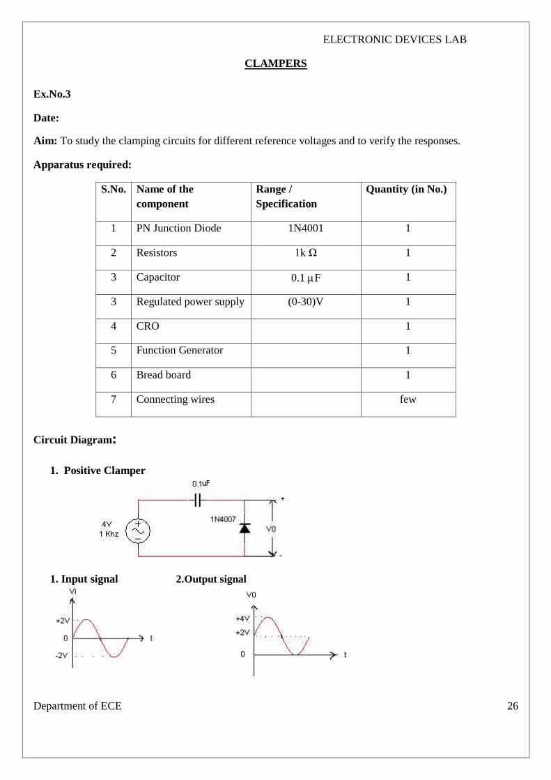
1. Positive Clamper
1. Input signal 2.Output signal

ELECTRONIC DEVICES LAB
Department of ECE 27
2. Negative Clamper
1. Input signal 2.Output signal
3. Positive Peak Clamping To VR=2V
4. Negative Peak Clamping To VR=-2V

ELECTRONIC DEVICES LAB
Department of ECE 28
5. Positive Peak Clamping To VR=0V
6. Negative Peak Clamping To VR= 0V
Theory:
Clamping circuits are circuits, which are used to clamp or fix the extremity of a periodic wave form
to some constant reference level. Clamping circuits may be one way clamps or two way clamps. The clamping circuits only changes the dc level of the input signal .It does not affect its shape. Clamping circuits may be positive voltage clamping circuits or negative voltage clamping circuits. In positive clamping, the negative extremity of the wave form is at the reference level and the entire wave form appears above the reference level. i.e. the output wave form is positively clamped with reference to the reference level.
In negative clamping the positive extremity of the wave form is fixed at the reference level and the entire wave form appears below the reference voltage. i.e. the output wave form is negatively clamped with reference to the reference level. The capacitors are essential in the clamping circuits. The difference between the clipping and clamping circuits is that while the clipper clips off an unwanted portion of the input wave form, the clipper simply clamps the maximum positive or negative peak of the wave form to a desired level.
Procedure:
1. Connections are made as per the circuit diagram.
2. I/P signal is applied to the circuit with the amplitude of 4v p-p and 1 KHz frequency.
3. The AC / DC push button switch of CRO is to be kept in DC mode.
4. Note down the o/p amplitude for each and every circuit.
5. The O/P waveforms are to be drawn on the graph sheet.
Result: Thus the responses of clamping circuits for different reference voltages were verified.

ELECTRONIC DEVICES LAB
Department of ECE 29
HALF WAVE RECTIFIER WITH AND WITHOUT FILTER
Ex.No.5
Date:
Aim: To verify the operation of half wave rectifier with and without capacitor filter and find Ripple factor.
Apparatus Required:
S.No. Name of the component Range / Specification Quantity
(in No.) 1 Diode IN4001 1
2 Resistance(or) DRB 470 1
3 CRO 1
4 Transformer 9-0-9 V 1
5 Capacitor 1000µF 1
6 Bread board and connecting wires
Circuit Diagram:

ELECTRONIC DEVICES LAB
Department of ECE 30
Model Graph:
Theory:
A rectifier is an electronic device that converts AC voltage into DC voltage. In other words, it
converts alternating current to direct current. A rectifier is used in almost all the electronic devices. Mostly it
is used to convert the main voltage into DC voltage in the power supply section. By using DC voltage
supply electronic devices work. According to the period of conduction, rectifiers are classified into two
categories: Half Wave Rectifier and Full Wave Rectifier. A Half wave rectifier contains only one PN
junction Diode. During the positive half cycle the diode is under forward bias condition and it conducts
current to RL (Load resistance). A voltage is developed across the load, which is same as the input AC
signal of the positive half cycle. Alternatively, during the negative half cycle the diode is under reverse bias
condition and there is no current flow through the diode. Only the AC input voltage appears across the load
and it is the net result which is possible during the positive half cycle. The output voltage pulsates the DC
voltage.
Procedure:
1. Connections are given as per the circuit diagram.
2. Apply AC main voltage to the primary of the transformer. Feed the rectified Output voltage to the
CRO and observe the Waveform.
3. Now connect the capacitor in parallel with load resistor and note down the amplitude and time period
of the waveform.
4. Plot the input, output waveforms on a graph sheet.
5. Calculate the ripple factor.

ELECTRONIC DEVICES LAB
Department of ECE 31
Tabular column:
S.No RL Vac
Time
Period of
input
signal
Vdc
Time
Period of
output
signal
Ripple Factor
Vac/Vdc
(with filter)
Ripple Factor
Vac/Vdc
(without filter)
1.
2.
3.
4.
Calculation:
Result: Thus the Input and Output Wave forms of Half wave rectifier with and without filter was observed and
its ripple factor was calculated.

ELECTRONIC DEVICES LAB
Department of ECE 32
FULL WAVE RECTIFIER WITH AND WITHOUT FILTER
Ex.No.6
Date:
Aim: To verify the operation of Full wave rectifier with and without capacitor filter and find Ripple factor.
Apparatus Required:
S.No. Name of the component Range / Specification Quantity
(in No.) 1 Diode IN4001 1
2 Resistance(or) DRB 470 1
3 CRO 1
4 Transformer 9-0-9 V 1
5 Capacitor 1000µF 1
6 Bread board and connecting wires
Circuit Diagram:

ELECTRONIC DEVICES LAB
Department of ECE 33
Model Graph:
Theory:
A rectifier is an electronic device that converts AC voltage into DC voltage. In other words, it
converts alternating current to direct current. A rectifier is used in almost all the electronic devices. Mostly it
is used to convert the main voltage into DC voltage in the power supply section. By using DC voltage
supply electronic devices work. According to the period of conduction, rectifiers are classified into two
categories: Half Wave Rectifier and Full Wave Rectifier. A Full Wave Rectifier is a circuit, which converts
an ac voltage into a pulsating dc voltage using both half cycles of the applied ac voltage. It uses two diodes
of which one conducts during one half cycle while the other conducts during the other half cycle of the
applied ac voltage. During the positive half cycle of the input voltage, diode D1 becomes forward biased and
D2 becomes reverse biased. Hence D1 conducts and D2 remains OFF. The load current flows through D1
and the voltage drop across RL will be equal to the input voltage. During the negative half cycle of the input
voltage, diode D1 becomes reverse biased and D2 becomes forward biased. Hence D1 remains OFF and D2
conducts. The load current flows through D2 and the voltage drop across RL will be equal to the input
voltage.
Procedure:
1. Connections are given as per the circuit diagram.
2. Apply AC main voltage to the primary of the transformer. Feed the rectified Output voltage to the
CRO and observe the Waveform.
3. Now connect the capacitor in parallel with load resistor and note down the amplitude and time period
of the waveform.
4. Plot the input, output waveforms on a graph sheet.
5. Calculate the ripple factor.
ELECTRONIC DEVICES LAB
Department of ECE 34
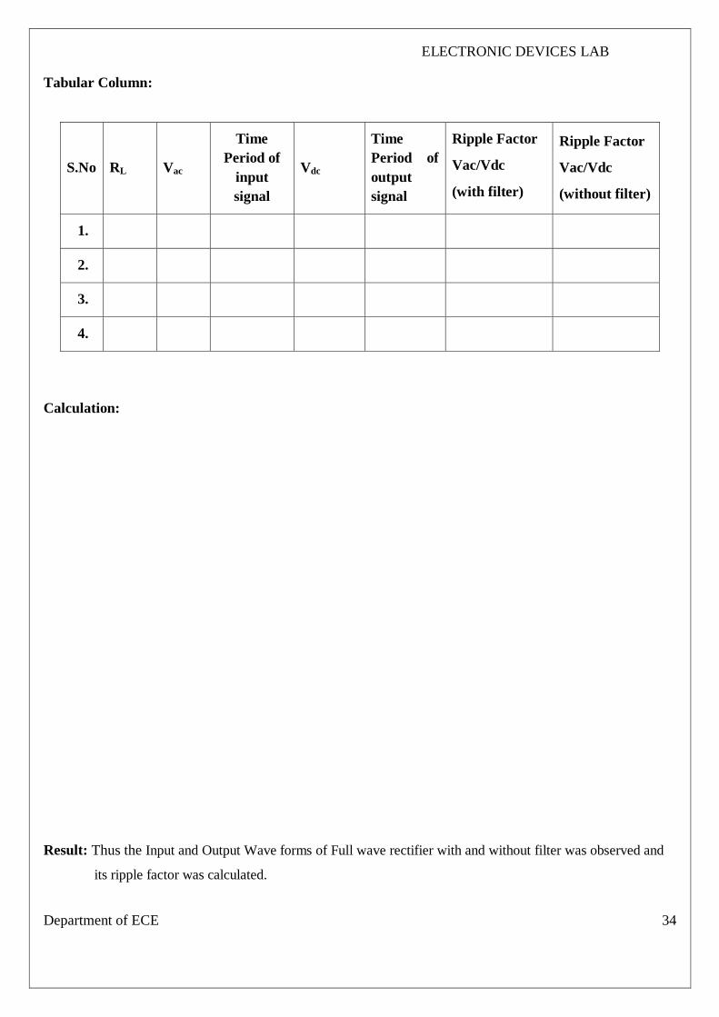
Tabular Column:
S.No RL Vac
Time
Period of
input
signal
Vdc
Time
Period of
output
signal
Ripple Factor
Vac/Vdc
(with filter)
Ripple Factor
Vac/Vdc
(without filter)
1.
2.
3.
4.
Calculation:
Result: Thus the Input and Output Wave forms of Full wave rectifier with and without filter was observed and
its ripple factor was calculated.

ELECTRONIC DEVICES LAB
Department of ECE 35
INPUT AND OUTPUT CHARACTERISTICS OF TRANSISTOR IN CB CONFIGURATION
Ex.No.7
Date:
Aim: To draw the input and output characteristics and to determine the hybrid parameters of a given
transistor in Common Base configuration.
Apparatus Required:
S.No. Name of the component Range / Specification Quantity
(in No.) 1. Transistor BC107 1
2. Resistance 1K 1
3. Regulated Power Supply (0-30)V 1
4. Ammeter (0-100)mA 2
5. Voltmeter (0-10)V 2
6. Bread board and connecting wires
Theory:
A transistor is a three terminal active device. T he terminals are emitter, base, collector. In CB
configuration, the base is common to both input (emitter) and output (collector). For normal operation,
the E-B junction is forward biased and C-B junction is reverse biased. With an increasing the reverse
collector voltage, the space-charge width at the output junction increases and the effective base width
„W‟ decreases. This phenomenon is known as “Early effect”. Then, there will be less chance for
recombination within the base region. With increase of charge gradient within the base region, the
current of minority carriers injected across the emitter junction increases. The current amplification
factor of CB configuration is given by, α= ΔIC/ ΔIE
Circuit Diagram:
ELECTRONIC DEVICES LAB
Department of ECE 36
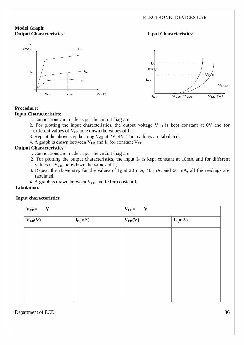
Model Graph:
Output Characteristics: Input Characteristics:
Procedure:
Input Characteristics:
1. Connections are made as per the circuit diagram.
2. For plotting the input characteristics, the output voltage VCB is kept constant at 0V and for
different values of VEB note down the values of IE.
3. Repeat the above step keeping VCB at 2V, 4V. The readings are tabulated.
4. A graph is drawn between VEB and IE for constant VCB.
Output Characteristics:
1. Connections are made as per the circuit diagram.
2. For plotting the output characteristics, the input IE is kept constant at 10mA and for different
values of VCB, note down the values of IC.
3. Repeat the above step for the values of IE at 20 mA, 40 mA, and 60 mA, all the readings are
tabulated.
4. A graph is drawn between VCB and Ic for constant IE.
Tabulation:
Input characteristics
VCB= V VCB= V
VEB(V) IE(mA) VEB(V) IE(mA)

ELECTRONIC DEVICES LAB
Department of ECE 37
Output characteristics
IE= (mA) IE= (mA)
VCB (V) Ic(mA) VCB (V) Ic(mA)
Calculation for h-parameters:
Result: Thus the Input and Output characteristics of BJT under common base configuration were
obtained and the hybrid parameters were calculated.
The h – parameters are:
hib = ______________, hfb = ________________, hrb = _________________, hob = ______________

ELECTRONIC DEVICES LAB
Department of ECE 38
INPUT AND OUTPUT CHARACTERISTICS OF TRANSISTOR IN CE CONFIGURATION
Ex.No.8
Date:
Aim:
To plot the input and output characteristics of a bipolar junction transistor in Common Emitter
configuration and to find its hybrid parameters.
Apparatus Required:
S.No. Name of the component Range / Specification Quantity
(in No.) 1. Transistor BC107 1
2. Resistance 1K 1
3. Regulated Power Supply (0-30)V 1
4. Ammeter (0-30)mA,(0-50)A 1
5. Voltmeter (0-30)V 2
6. Bread board 1
7. Connecting wires few
Circuit Diagram:
Input Characteristics: Output Characteristics:

ELECTRONIC DEVICES LAB
Department of ECE 39
Procedure:
Input Characteristics:
1. Connect the transistor in CE configuration as per circuit diagram
2. Keep output voltage VCE at constant voltage by varying VCC.
3. Varying VBE gradually, note down both base current IB and VBE.
4. Repeat above procedure (step 3) for various values of VCE.
5. Plot the input characteristics by taking VBE on Y-axis and IB on X-axis at Constant VCE.
Output Characteristics:
1. Make the connections as per circuit diagram.
2. By varying VBE keep the base current IB constant.
3. Varying VCC gradually, note down the readings of collector-current (IC) and collector-
emitter voltage (VCE).
4. Repeat above procedure (step 3) for different values of Ib
5. Plot the output characteristics by taking VCE on x-axis and IC on y-axis by taking IB as a
constant parameter.
Tabular Column:
Input Characteristics:
VCE = 0V VCE = 5V
VBE (Volts) IB (µA) VBE (Volts) IB (µA)

ELECTRONIC DEVICES LAB
Department of ECE 40
Output Characteristics:
IB = 0 µA IB = 20 µA IB = 40 µA
VCE (Volts) IC (mA) VCE (Volts) IC (mA) VCE (Volts) IC (mA)
Calculation for h-parameters:
Result: Thus the Input and output characteristics of BJT under common emitter configuration was
obtained and its hybrid parameters were calculated.
The h – parameters are
hie = ______________, hfe = __________________, hre = _________________, hoe = __________________
ELECTRONIC DEVICES LAB
Department of ECE 41
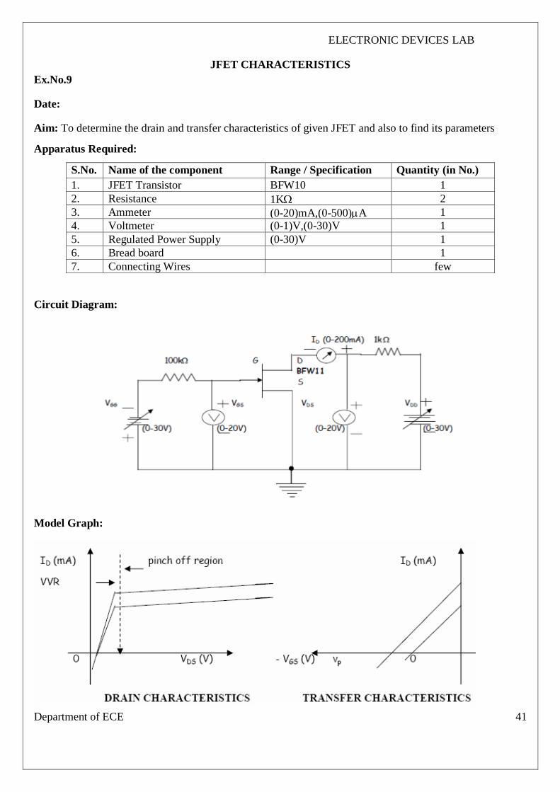
JFET CHARACTERISTICS
Ex.No.9
Date:
Aim: To determine the drain and transfer characteristics of given JFET and also to find its parameters
Apparatus Required:
S.No. Name of the component Range / Specification Quantity (in No.)
1. JFET Transistor BFW10 1
2. Resistance 1K 2
3. Ammeter (0-20)mA,(0-500)A 1
4. Voltmeter (0-1)V,(0-30)V 1
5. Regulated Power Supply (0-30)V 1
6. Bread board 1
7. Connecting Wires few
Circuit Diagram:
Model Graph:
ELECTRONIC DEVICES LAB
Department of ECE 42
Tabular Column:
Drain Characteristics:
Vgs= Vgs= Vgs=
VDS (V) ID (mA) VDS (V) ID (mA) VDS (V) ID (mA)
Transfer Characteristics:
VDS = VDS =
VGS (V) ID (mA) Vgs (V) ID (mA)

ELECTRONIC DEVICES LAB
Department of ECE 43
Theory:
The junction FET has a channel consisting of N-type semiconductor or P-type semiconductor
material and the gate is made of the opposite semiconductor type. The N-channel is doped with donor
impurities where the flow of current through the channel is negative in the form of electrons. The P-
channel is doped with acceptor impurities on where the flow of current is positive in the form of holes.
Since electrons have a higher mobility through a conductor compared to holes, N-channel JFETs have
a greater channel conductivity compared to their equivalent P-channel type.
The input impedance is extremely high since the gate junction is reverse biased and because
there is no minority carrier contribution to the flow through the device. The depletion of charge
carriers from the N-channel serves as the control element for the JFET. The majority carriers from a
larger depletion zone around the gate are depleted when the gate is made more negative. For a given
value of source-to-drain voltage, this reduces the current flow.
Procedure:
Drain Characteristics:
1. Connections are made as per the circuit diagram.
2. Set gate voltage VGS as constant, vary the drain voltage VDS insteps of 1V & note down the
corresponding drain current ID.
3. Repeat the above procedure for VGS=0V, 2V.
4. Plot the graph for a constant VDS Vs ID.
5. Find the drain resistance (rd) = ∆VDS/∆ID.
Transfer Characteristics:
1. Connections are made as per the circuit diagram.
2. Set gate voltage VDS as constant, vary the gate voltage VGS in step of 1V & note down the
corresponding drain current ID.
3. Repeat the above procedure for VDS=5V, 10V.
4. Plot the graph for VGS Vs ID.
5. Find the Trans conductance (gm) gm = ∆ID/∆VGS.
Calculation:
Trans conductance (gm) =ΔID/ ΔVGS =
Drain resistance (rd) = ΔVDS/ ΔID=
Amplification Factor (µ) = gm x rd =
Result: Thus the drain and transfer characteristics of JFET was drawn and the parameters were determined.
1. Drain resistance (rd)=............
2. Trans conductance (gm)=............
3. Amplification factor (μ)=............
ELECTRONIC DEVICES LAB
Department of ECE 44
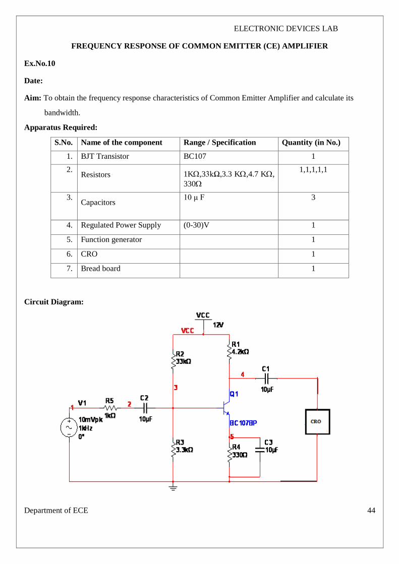
FREQUENCY RESPONSE OF COMMON EMITTER (CE) AMPLIFIER
Ex.No.10
Date:
Aim: To obtain the frequency response characteristics of Common Emitter Amplifier and calculate its
bandwidth.
Apparatus Required:
S.No. Name of the component Range / Specification Quantity (in No.)
1. BJT Transistor BC107 1
2. Resistors 1K,33kΩ,3.3 K,4.7 K,
330
1,1,1,1,1
3. Capacitors
10 μ F
3
4. Regulated Power Supply (0-30)V 1
5. Function generator 1
6. CRO 1
7. Bread board
1
Circuit Diagram:

ELECTRONIC DEVICES LAB
Department of ECE 45
Tabular Column:
Keep the input voltage constant, Vin =
S.No Frequency
(in Hz)
Output
Voltage
(in volts)
Gain
Av = Vo/Vi
Gain in dB =
20 log(Vo/Vin)
(in dB)
Calculation of Bandwidth:
-3dB Bandwidth = fH - fL

ELECTRONIC DEVICES LAB
Department of ECE 46
Theory:
The CE amplifier provides high gain & wide frequency response. The emitter lead is common to
both input and output circuits and is grounded. The emitter base circuit is forward biased. The collector
current is controlled by the base current rather than emitter current. The input signal is applied to base
terminal of the transistor and amplifier output is taken across collector terminal. A very small change in base
current produces a much larger change in collector current. Frequency response of an amplifier is defined as
the variation of gain with respective frequency.
The gain of the amplifier increases as the frequency increases from zero till it becomes maximum at
lower cutoff frequency and remains constant till higher cutoff frequency and then it falls again as the
frequency increases. At low frequencies the reactance of coupling capacitor Cc is quite high and hence very
small part of signal will pass through from one stage to the next stage. At high frequencies the reactance of
inter electrode capacitance is very small and behaves as a short circuit.
This increases the loading effect on next stage and service to reduce the voltage gain due to these
reasons the voltage gain drops at high frequencies. At mid frequencies the effect of coupling capacitors is
negligible and acts like short circuit, where as inter electrode capacitors acts like open circuit. So, the circuit
becomes resistive at mid frequencies and the voltage gain remains constant during this range.
Procedure:
1. Connections are given as per the circuit diagram.
2. Set the Input Voltage Vin as Constant in Function Generator.
3. Vary the Frequency Values in Function Generator and note down the Output amplitude for
different values of input frequency using CRO or Multimeter.
4. Calculate the Gain in dB by using the formula 20log (Vo/Vin) and tabulate the values.
5. Plot the frequency response graph in Semilog graph sheet and determine its -3dB bandwidth.
Result: Thus the frequency response of Single Stage Common Emitter (CE) Amplifier was obtained
and its bandwidth was calculated as _______________.

ELECTRONIC DEVICES LAB
Department of ECE 47
FREQUENCY RESPONSE OF COMMON COLLECTOR (CC) AMPLIFIER
Ex.No.11
Date:
Aim:
To obtain the frequency response of Common Collector Amplifier and calculate its band width.
Apparatus Required:
S.No. Name of the component Range / Specification Quantity (in No.)
1. BJT Transistor BC107 1
2. Resistors 1K,3.3 K,4.7 K, 470
1,3,1,1,1
3. Capacitors 10 μ F
2
4. Regulated Power Supply (0-30)V 1
5. Function generator 1
6. CRO
1
7. Bread board
1
Circuit Diagram:

ELECTRONIC DEVICES LAB
Department of ECE 48
Theory:
In common-collector amplifier the input is given at the base and the output is taken at the emitter. In
this amplifier, there is no phase inversion between input and output. The input impedance of the CC
amplifier is very high and output impedance is low. The voltage gain is less than unity. Here the collector is
at ac ground and the capacitors used must have a negligible reactance at the frequency of operation. This
amplifier is used for impedance matching and as a buffer amplifier. This circuit is also known as emitter
follower. The most common use of the emitter follower is as a circuit, which performs the function of
impedance transformation over a wide range of frequencies.
Procedure:
1. Connect the circuit as shown in circuit diagram
2. Apply the input of 20mV peak-to-peak and 1 KHz frequency using Function Generator
3. Measure the Output Voltage Vo (p-p) Tabulate the readings in the tabular form.
4. For plotting the frequency response the input voltage is kept Constant at 20mV peak-to-peak and the
frequency is varied from 100Hz to 1MHz Using function generator
5. All the readings are tabulated and voltage gain in dB is calculated by Using The expression Av=20
log10 (V0/Vi)
6. A graph is drawn by taking frequency on x-axis and gain in dB on y-axis On Semi-log graph.
7. The Bandwidth of the amplifier is calculated from the graph using the Expression,
Model graph:

ELECTRONIC DEVICES LAB
Department of ECE 49
Tabular Column:
Keep the input voltage constant, Vin =
S.No Frequency
(in Hz)
Output
Voltage
(in volts)
Gain
Av = Vo/Vi
Gain in dB =
20 log(Vo/Vin)
(in dB)
Calculation of Bandwidth:
-3dB Bandwidth = fH - fL
Result: Thus the frequency response of Single Stage Common Collector (CC) Amplifier was obtained
and its bandwidth was calculated as _______________.

ELECTRONIC DEVICES LAB
Department of ECE 50
FREQUENCY RESPONSE OF COMMON SOURCE FET AMPLIFIER
Ex.No.12
Date:
Aim: To obtain the frequency response of Common Source FET Amplifier and to calculate its band width.
Apparatus Required:
S.No. Name of the component Range / Specification Quantity (in No.)
1. FET Transistor BFW10/11 1
2. Resistors 1.5K,1M,6.8k
10 K,4.7 K
1,1,1
3. Capacitors 0.1μ F,47µF 1,1
4. Regulated Power Supply (0-30)V 1
5. Function generator 1
6. CRO 1
7. Bread board 1
8. Connecting Wires few
Circuit Diagram:

ELECTRONIC DEVICES LAB
Department of ECE 51
Theory:
The FET is a type of transistor commonly used for weak signal amplification. The device can
amplify analog or digital signals. It can also switch DC or function as an oscillator. In the FET current flows
along a semiconductor path called the channel. At one end of the channel, there is an electrode called source.
At the other end of the channel there is an electrode called the drain. Frequency response of an
amplifier is defined as the variation of gain with respective frequency. The gain of the amplifier increases as
the frequency increases from zero till it becomes maximum at lower cut-off frequency and remains constant
till higher cut-off frequency and then it falls again as the frequency increases.
At mid frequencies the effect of coupling capacitors is negligible and acts like short circuit, whereas
inter electrode capacitors acts like open circuit. So, the circuit becomes resistive at mid frequencies and the
voltage gain remains constant during this range
Procedure:
1. Connections are made as per the circuit diagram.
2. Set Vdd 10v and adjust the Vds to 5v.
3. A signal of 2 KHz frequency and 20mV peak-to-peak is applied at the input of amplifier.
4. Output is taken at drain and gain is calculated by using the expression, Av=V0/Vi
5. Voltage gain in dB is calculated by using the expression, Av=20log 10(V0/Vi)
6. Plot Av vs. Frequency, The Bandwidth of the amplifier is calculated.
Model graph:

ELECTRONIC DEVICES LAB
Department of ECE 52
Tabular Column:
Keep the input voltage constant, Vin =
S.No Frequency
(in Hz)
Output
Voltage
(in volts)
Gain
Av = Vo/Vi
Gain in dB =
20 log(Vo/Vin)
(in dB)
Calculation of Bandwidth:
-3dB Bandwidth = fH - fL
Result: Thus the frequency response of Common Source (CS) Amplifier was obtained and its bandwidth
was calculated as _______________.