signal integrity modeling and simulation for ic/package co … · 2004-11-23 · 10 signal...
TRANSCRIPT

Signal Integrity Modeling and Simulationfor
IC/Package Co-Design
Ching-Chao HuangOptimal Corp.
October 24, 2004

2
Why IC and package co-design?
The same IC in different packages may not workPackage is the biggest discontinuity in entire channel
Package is to be selected before IC is conceivedMany design parameters affect package decision
No. and assignment of I/O and P/G pads
Wire-bondor flip-chip
Maximumfrequency and power
Ri, Ci, atInput receiver
IR drop andground bounce
Stackup,width and spacing
Cost vs.performance
RLGCparasitics
Thermal andmechanical
IC Package

Signal Integrity Issuesfor
IC/Package Co-Design

4
Issue 1: Want to optimize receiver inputs at silicon pads
High impedance of bond wires can compensate ESD and receiver’s input capacitance and help open up eyes?
Optimize receiver inputs here.
IC
Package
PCB
Bond-Wire vs. Flip-Chip Package

5
Issue 2: Want to optimize driver outputs at package pins, not silicon pads
Need accurate package models!
Do not optimize driver outputs here.
PCB
IC
Package
Instead, optimize driver’s voltage swing, rise/fall time, and duty cycle here.

6
Issue 3: Hard to correlate measurement with simulation at silicon pads
Rely on modeling and simulation to infer the actual received waveforms on-chip
PCB
IC
Package
In actual system operation, we can only probe here.
What are the actual received waveforms here?
7
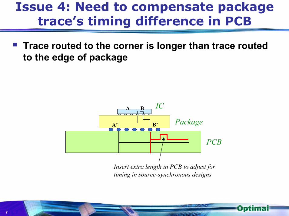
Issue 4: Need to compensate package trace’s timing difference in PCB
Trace routed to the corner is longer than trace routed to the edge of package
PCB
IC
Package
A B
A’ B’
Insert extra length in PCB to adjust fortiming in source-synchronous designs
8
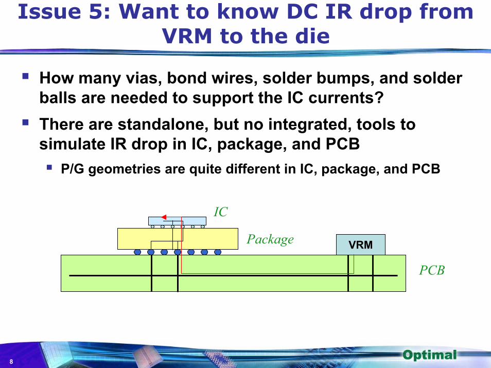
Issue 5: Want to know DC IR drop from VRM to the die
How many vias, bond wires, solder bumps, and solder balls are needed to support the IC currents?There are standalone, but no integrated, tools to simulate IR drop in IC, package, and PCB
P/G geometries are quite different in IC, package, and PCB
PCB
IC
Package VRM
Methodologies and EDA Softwarefor
Signal and Power Integrity Simulation

10
Signal Integrity(Multi-Giga-Hertz Transmission)
Create S-parameter models for time-domain simulations
Accurate over a wide bandwidthGood for both design and verification
Insertion and return losses are key design specs.
FlexibleCan perform many what-if analyses by combining or varying other component models in the channelMultiple vendor tools to choose from
FrequencyDomain
TimeDomain
CAD Data.mcm, .brd, Gerber, …
Optimal O-WaveAnsoft HFSS
S, Y, Z Parameters
Agilent ADSAWR Microwave Office
Apache NspiceSynopsys Hspice
Cadence Spectre RF
Time-Domain WaveformsEye Diagrams, …

11
IC and package co-design for timing closure (TSMC reference flow 5.0)
Delay difference in package needs to be compensated on the board.
PackageRLGC ExtractionOptimal PakSi-E
SDF
StaticTiming Analysis
SPICE Netlists
CircuitSimulation
Package Layout Cadence Allegro
Package DesignDatabase
I/O ModelRDL Parasitics
Trace LengthCompensation
RulesDelay Time Table
12
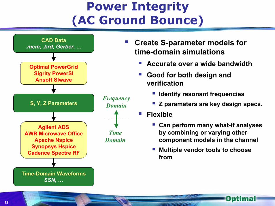
Power Integrity(AC Ground Bounce)
Create S-parameter models for time-domain simulations
Accurate over a wide bandwidthGood for both design and verification
Identify resonant frequenciesZ parameters are key design specs.
FlexibleCan perform many what-if analyses by combining or varying other component models in the channelMultiple vendor tools to choose from
CAD Data.mcm, .brd, Gerber, …
Optimal PowerGridSigrity PowerSIAnsoft SIwave
S, Y, Z Parameters
Agilent ADSAWR Microwave Office
Apache NspiceSynopsys Hspice
Cadence Spectre RF
FrequencyDomain
TimeDomain
Time-Domain WaveformsSSN, …

13
Meeting the Z11 design spec.
Need to compute Z11 under various source excitations (e.g., group all solder bumps vs. excite one solder bump at a time)The package resonance is critical if the board is considered equi-potential.
Z11 Z11
Complex 8-layer BGA package
0
10
20
30
40
50
60
0 2 4 6 8 10
Freq (GHz)
| Z11
| (o
hm)
Tie all solder bumps togetherOpen all but one solder bump
Assume same potential at the board.

14
Quantifying extraction accuracy
Geometry is to be modeled closely in its entirety
Resonance depends on the shape and size of structureUse triangular, not rectangular, meshes
Have good agreements with other field solvers
Match 2D quasi-static solver in long narrow tracesMatch 3D full-wave solver in simple 3D structures
Have good correlation with measurements
Hard to probe the package directly with the right probes and correct open/short conditions
-60
-40
-20
0
0 4 8 12 16 20Freq (GHz)
S11
(dB
)
PowerGrid (Fringe RLGC) Fringe CNo Fringe QSolve (2D Solver)
5 mils1
3 ε = 4; tan δ = 0.02ε = 1
200
Unit in mils
S12 of a Square Plate
-20-16-12
-8-40
0 5 10 15 20Freq (GHz)
S12
(dB
)
PowerGrid (Fringe RLGC) Fringe CNo Fringe O-Wave (3D Full-Wave)
200
200
100
100
Port A
Port B
4 milε = 4.4tan δ = 0.02
1
+
+

15
Power Integrity(DC IR Drop)
Package’s DC IR drop is crucial for power integrity
Need voltage, current, current density distributions, and equivalent resistive networksStructure is to be modeled closely by triangular, not rectangular, meshes
CAD Data.mcm, .brd, Gerber, …
Optimal PowerGrid
VoltageCurrent
Current DensityResistive Network
Voltage Contour Current Density

16
IC and package co-design for DC power closure (TSMC reference flow 5.0)
IC and package extraction software provide chip and package loading for each other.
Package Layout Cadence Allegro
In-PackageIR Drop Analysis
Optimal PowerGrid
SPICE Netlists
On-ChipIR Drop Analysis
Cadence VoltageStorm
Package DesignDatabase
Current Loads at Bumps or Bondwires
In-PackageCurrent Density
Plot
On-ChipCurrent Density
Plot
17
More EDA tools
Integrated layout, extraction and simulationCadence Allgero Package Designer 620 and Allegro Package SI 620
Direct time-domain simulationCST Microwave StudioSigrity Speed2000
Simulation frameworkAWR Microwave Office with EM socket interface
LinksSynopsys Encore + Ansoft TPA

18
Cadence Allegro Package Designer 620 and Allegro Package SI 620
Simultaneous physical and electrical designsLEF/DEF interfaceBuilt-in 3D field solver and simulation
19
Summary
Why IC/package co-design?Same IC in different packages may not work
Signal integrity issues that affect IC/package co-designWant to optimize receiver inputs at silicon pads and driver outputs at package pinsWant to compensate package trace’s timing difference in PCB
Methodologies and EDA software for signal and power integrity simulation
Using S parameters for time-domain simulation allows multiple vendor tools to choose fromNeed to model geometries closely for accurate IR drop and groundbounce analyses
More EDA toolsCadence Allegro Package SI 620 has built-in 3D solver and allows simultaneous physical and electrical designs