sikder, md ashif accepted thesis 7-20-16 su16
TRANSCRIPT

Emerging Technologies in On-Chip and Off-Chip Interconnection Network
A thesis presented to
the faculty of
the Russ College of Engineering and Technology of Ohio University
In partial fulfillment
of the requirements for the degree
Master of Science
Md Ashif Iqbal Sikder
August 2016
© 2016 Md Ashif Iqbal Sikder. All Rights Reserved.
2
This thesis titled
Emerging Technologies in On-Chip and Off-Chip Interconnection Network
by
MD ASHIF IQBAL SIKDER
has been approved for
the School of Electrical Engineering and Computer Science
and the Russ College of Engineering and Technology by
Avinash Karanth Kodi
Associate Professor of Electrical Engineering and Computer Science
Dennis Irwin
Dean, Russ College of Engineering and Technology
3
Abstract
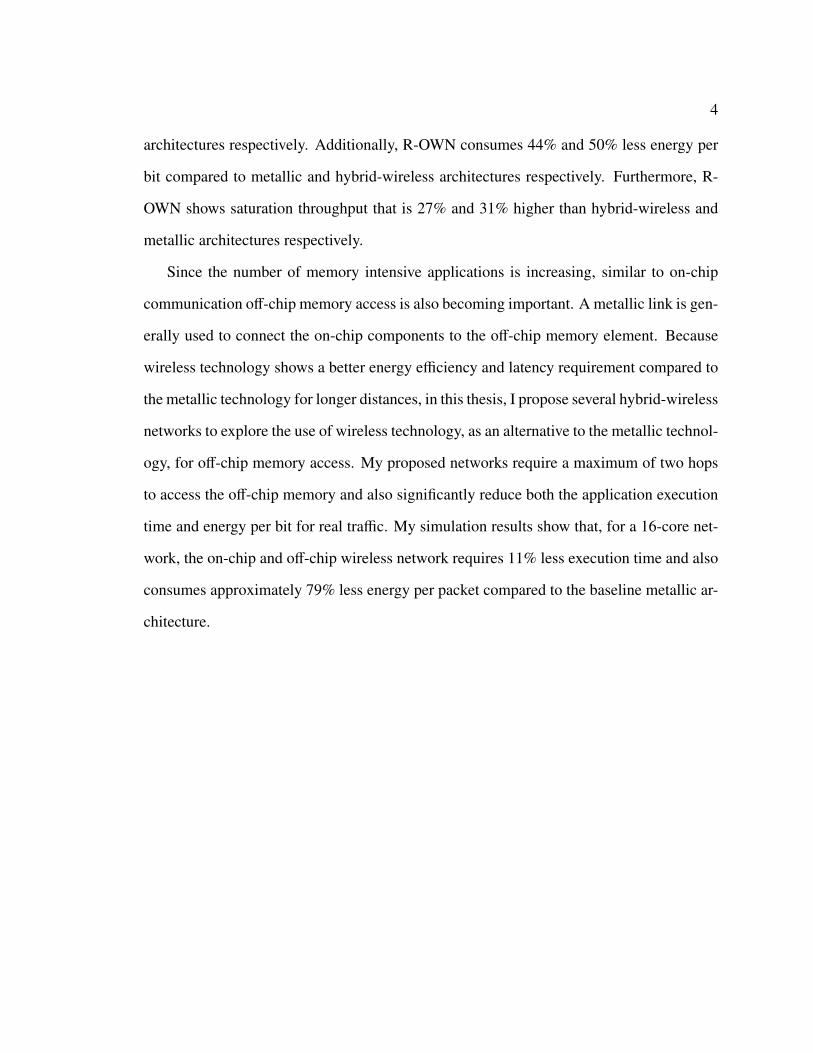
SIKDER, MD ASHIF IQBAL, M.S., August 2016, Electrical Engineering
Emerging Technologies in On-Chip and Off-Chip Interconnection Network (80 pp.)
Director of Thesis: Avinash Karanth Kodi
The number of processing cores on a chip is increasing with the scaling down of
transistors to meet the computation demand. This increase requires a scalable and an energy
and latency efficient network to provide a reliable communication between the cores.
Traditionally, metallic interconnection networks are used to connect the cores. However,
according to the International Technology Roadmap for Semiconductor (ITRS), metallic
interconnection networks would not be able to meet the future on-chip communication
demands due to the energy and latency constraints. Thus, this thesis focuses on the novel
on-chip network designs employing the emerging technologies, such as wireless and optics,
to provide a scalable and an energy and latency efficient network. In this thesis, I propose
an on-chip network architecture called Optical and Wireless Network-on-Chip (OWN)
and extend OWN to construct Reconfigurable Optical and Wireless Network-on-Chip (R-
OWN) architecture. OWN and R-OWN both leverage the advantages of optics and wireless
technologies while circumventing the limitations of these technologies. The end result is
that OWN and R-OWN both can provide a maximum of three hops communication between
any two cores for a 256 to 1024 core networks. My simulation results with synthetic
traffic demonstrate that, for 1024-core architectures, OWN requires 34% more area than
hybrid-wireless architectures and 35% less area than hybrid-photonic architectures [1].
In addition, OWN consumes 30% less energy per bit than hybrid-wireless architectures
and 14% more energy per bit than hybrid-photonic architectures [1]. Moreover, OWN
shows 8% and 28% improvement in saturation throughput compared to hybrid-wireless
and metallic architectures respectively [1]. On the other hand, for 256-core architectures,
R-OWN requires 3.9% and 12% less area compared to metallic and hybrid-wireless
4
architectures respectively. Additionally, R-OWN consumes 44% and 50% less energy per
bit compared to metallic and hybrid-wireless architectures respectively. Furthermore, R-
OWN shows saturation throughput that is 27% and 31% higher than hybrid-wireless and
metallic architectures respectively.
Since the number of memory intensive applications is increasing, similar to on-chip
communication off-chip memory access is also becoming important. A metallic link is gen-
erally used to connect the on-chip components to the off-chip memory element. Because
wireless technology shows a better energy efficiency and latency requirement compared to
the metallic technology for longer distances, in this thesis, I propose several hybrid-wireless
networks to explore the use of wireless technology, as an alternative to the metallic technol-
ogy, for off-chip memory access. My proposed networks require a maximum of two hops
to access the off-chip memory and also significantly reduce both the application execution
time and energy per bit for real traffic. My simulation results show that, for a 16-core net-
work, the on-chip and off-chip wireless network requires 11% less execution time and also
consumes approximately 79% less energy per packet compared to the baseline metallic ar-
chitecture.

5
Acknowledgements
First, I would like to thank my parents for always supporting me. Second, I would like
to thank my supervisor Dr. Avinash Kodi, for relentlessly pushing me. Third, I would like
to thank my committee members- Dr. Savas Kaya, Dr. Jeffrey Dill, and Dr. David Ingram
for their valuable time. Lastly, I would like to thank NSF as this thesis work was partially
supported by NSF grants CCF-1054339 (CAREER), CCF-1420718, CCF-1318981, ECCS-
1342657, and CCF-1513606.
6
Table of Contents
Page
Abstract . . . . . . . . . . . . . . . . . . . . . . . . . . . . . . . . . . . . . . . . . 3
Acknowledgements . . . . . . . . . . . . . . . . . . . . . . . . . . . . . . . . . . . 5
List of Tables . . . . . . . . . . . . . . . . . . . . . . . . . . . . . . . . . . . . . . 8
List of Figures . . . . . . . . . . . . . . . . . . . . . . . . . . . . . . . . . . . . . . 9
List of Acronyms . . . . . . . . . . . . . . . . . . . . . . . . . . . . . . . . . . . . 10
1 Introduction . . . . . . . . . . . . . . . . . . . . . . . . . . . . . . . . . . . . . 111.1 Network-on-Chip (NoC) . . . . . . . . . . . . . . . . . . . . . . . . . . . 121.2 Issues in NoC . . . . . . . . . . . . . . . . . . . . . . . . . . . . . . . . . 15
1.2.1 Energy . . . . . . . . . . . . . . . . . . . . . . . . . . . . . . . . 151.2.2 Latency . . . . . . . . . . . . . . . . . . . . . . . . . . . . . . . . 161.2.3 Metallic Interconnects . . . . . . . . . . . . . . . . . . . . . . . . 16
1.3 Emerging Technologies in Interconnection Network: Wireless and Photonics 171.3.1 Wireless Interconnection Network . . . . . . . . . . . . . . . . . . 171.3.2 Photonic Interconnection Network . . . . . . . . . . . . . . . . . . 20
1.4 Proposed Research and Major Contributions . . . . . . . . . . . . . . . . . 221.4.1 Heterogeneity in Interconnection Network . . . . . . . . . . . . . . 231.4.2 Off-Chip Interconnection Network . . . . . . . . . . . . . . . . . . 241.4.3 Key Contributions and Thesis Organization . . . . . . . . . . . . . 25
2 Heterogeneous Network-on-Chip . . . . . . . . . . . . . . . . . . . . . . . . . . 262.1 OWN Architecture . . . . . . . . . . . . . . . . . . . . . . . . . . . . . . 27
2.1.1 64-Core OWN Architecture: Cluster . . . . . . . . . . . . . . . . . 282.1.2 1024-Core OWN Architecture: Cluster and Group . . . . . . . . . 292.1.3 Intra-Group and Inter-Group Communication . . . . . . . . . . . . 322.1.4 Deadlock Free Routing . . . . . . . . . . . . . . . . . . . . . . . . 33
2.2 Technology for OWN: Wireless and Optical . . . . . . . . . . . . . . . . . 352.2.1 Wireless Technology . . . . . . . . . . . . . . . . . . . . . . . . . 352.2.2 Photonics Technology . . . . . . . . . . . . . . . . . . . . . . . . 37
2.3 Reconfigurable-OWN (R-OWN) . . . . . . . . . . . . . . . . . . . . . . . 382.3.1 256-Core OWN Architecture . . . . . . . . . . . . . . . . . . . . . 382.3.2 256-Core R-OWN Architecture . . . . . . . . . . . . . . . . . . . 402.3.3 Routing Mechanism of 256-Core R-OWN . . . . . . . . . . . . . . 422.3.4 Deadlock Free Routing . . . . . . . . . . . . . . . . . . . . . . . . 44
7
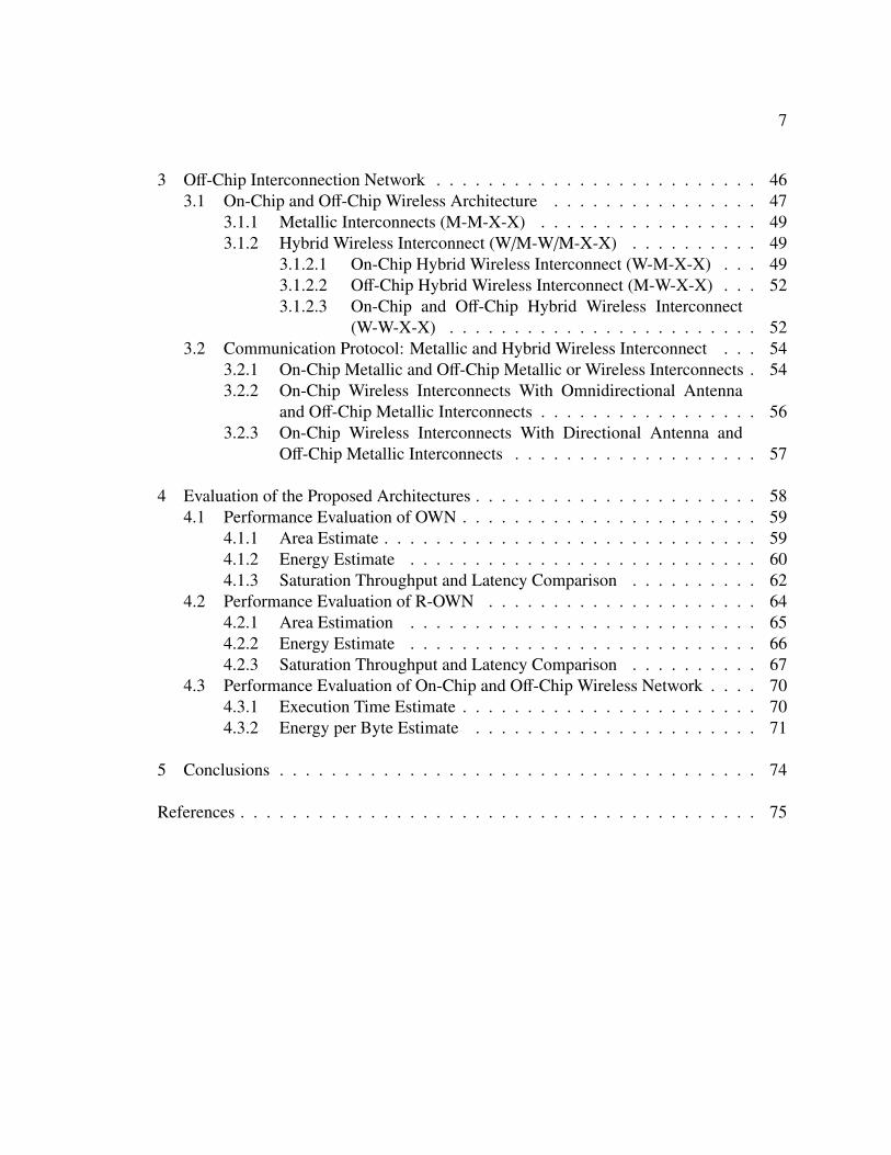
3 Off-Chip Interconnection Network . . . . . . . . . . . . . . . . . . . . . . . . . 463.1 On-Chip and Off-Chip Wireless Architecture . . . . . . . . . . . . . . . . 47
3.1.1 Metallic Interconnects (M-M-X-X) . . . . . . . . . . . . . . . . . 493.1.2 Hybrid Wireless Interconnect (W/M-W/M-X-X) . . . . . . . . . . 49
3.1.2.1 On-Chip Hybrid Wireless Interconnect (W-M-X-X) . . . 493.1.2.2 Off-Chip Hybrid Wireless Interconnect (M-W-X-X) . . . 523.1.2.3 On-Chip and Off-Chip Hybrid Wireless Interconnect
(W-W-X-X) . . . . . . . . . . . . . . . . . . . . . . . . 523.2 Communication Protocol: Metallic and Hybrid Wireless Interconnect . . . 54
3.2.1 On-Chip Metallic and Off-Chip Metallic or Wireless Interconnects . 543.2.2 On-Chip Wireless Interconnects With Omnidirectional Antenna
and Off-Chip Metallic Interconnects . . . . . . . . . . . . . . . . . 563.2.3 On-Chip Wireless Interconnects With Directional Antenna and
Off-Chip Metallic Interconnects . . . . . . . . . . . . . . . . . . . 57
4 Evaluation of the Proposed Architectures . . . . . . . . . . . . . . . . . . . . . . 584.1 Performance Evaluation of OWN . . . . . . . . . . . . . . . . . . . . . . . 59
4.1.1 Area Estimate . . . . . . . . . . . . . . . . . . . . . . . . . . . . . 594.1.2 Energy Estimate . . . . . . . . . . . . . . . . . . . . . . . . . . . 604.1.3 Saturation Throughput and Latency Comparison . . . . . . . . . . 62
4.2 Performance Evaluation of R-OWN . . . . . . . . . . . . . . . . . . . . . 644.2.1 Area Estimation . . . . . . . . . . . . . . . . . . . . . . . . . . . 654.2.2 Energy Estimate . . . . . . . . . . . . . . . . . . . . . . . . . . . 664.2.3 Saturation Throughput and Latency Comparison . . . . . . . . . . 67
4.3 Performance Evaluation of On-Chip and Off-Chip Wireless Network . . . . 704.3.1 Execution Time Estimate . . . . . . . . . . . . . . . . . . . . . . . 704.3.2 Energy per Byte Estimate . . . . . . . . . . . . . . . . . . . . . . 71
5 Conclusions . . . . . . . . . . . . . . . . . . . . . . . . . . . . . . . . . . . . . 74
References . . . . . . . . . . . . . . . . . . . . . . . . . . . . . . . . . . . . . . . . 75
8
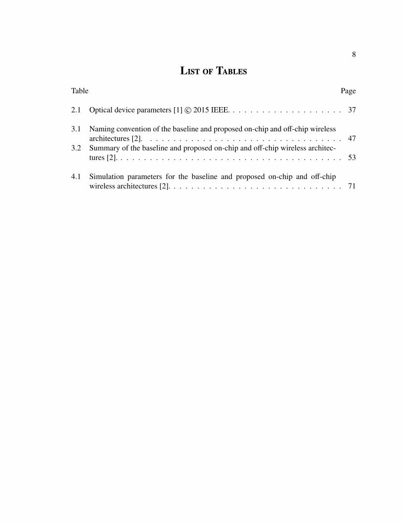
List of Tables
Table Page
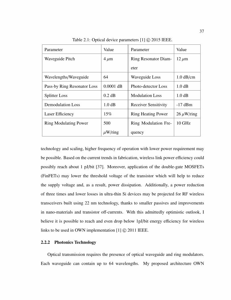
2.1 Optical device parameters [1]© 2015 IEEE. . . . . . . . . . . . . . . . . . . . 37
3.1 Naming convention of the baseline and proposed on-chip and off-chip wirelessarchitectures [2]. . . . . . . . . . . . . . . . . . . . . . . . . . . . . . . . . . 47
3.2 Summary of the baseline and proposed on-chip and off-chip wireless architec-tures [2]. . . . . . . . . . . . . . . . . . . . . . . . . . . . . . . . . . . . . . . 53
4.1 Simulation parameters for the baseline and proposed on-chip and off-chipwireless architectures [2]. . . . . . . . . . . . . . . . . . . . . . . . . . . . . . 71
9
List of Figures
Figure Page
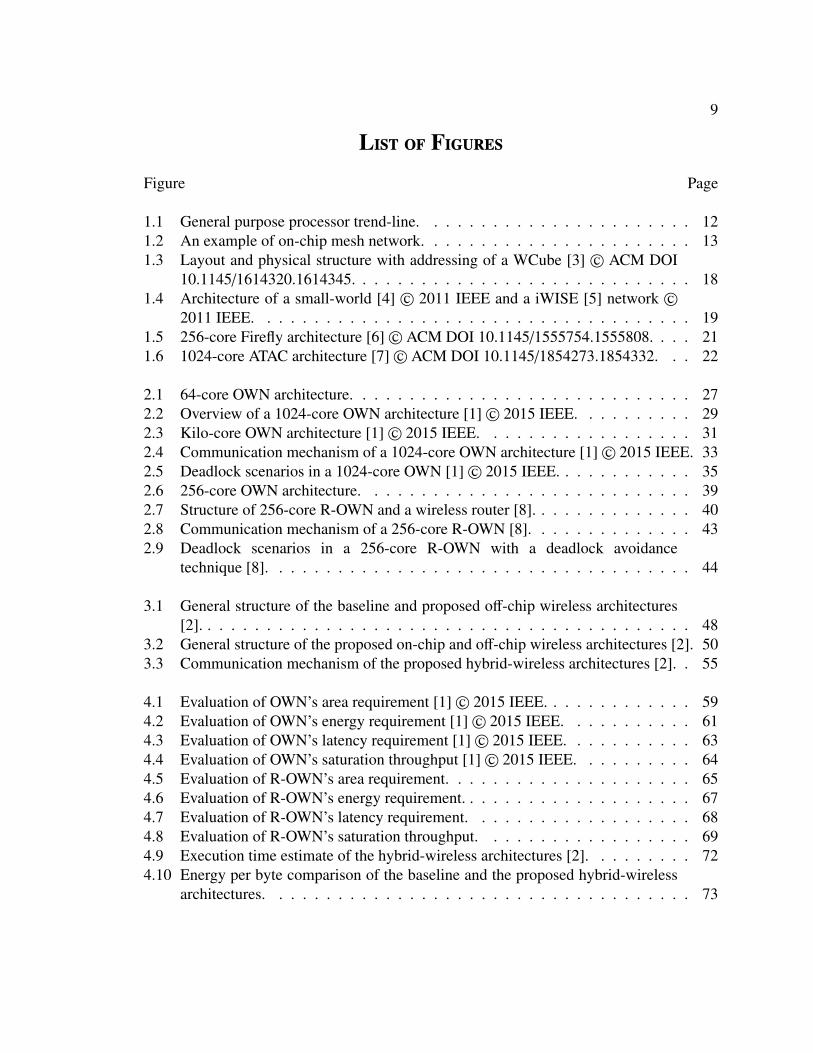
1.1 General purpose processor trend-line. . . . . . . . . . . . . . . . . . . . . . . 121.2 An example of on-chip mesh network. . . . . . . . . . . . . . . . . . . . . . . 131.3 Layout and physical structure with addressing of a WCube [3] © ACM DOI
10.1145/1614320.1614345. . . . . . . . . . . . . . . . . . . . . . . . . . . . . 181.4 Architecture of a small-world [4] © 2011 IEEE and a iWISE [5] network ©
2011 IEEE. . . . . . . . . . . . . . . . . . . . . . . . . . . . . . . . . . . . . 191.5 256-core Firefly architecture [6]© ACM DOI 10.1145/1555754.1555808. . . . 211.6 1024-core ATAC architecture [7]© ACM DOI 10.1145/1854273.1854332. . . 22
2.1 64-core OWN architecture. . . . . . . . . . . . . . . . . . . . . . . . . . . . . 272.2 Overview of a 1024-core OWN architecture [1]© 2015 IEEE. . . . . . . . . . 292.3 Kilo-core OWN architecture [1]© 2015 IEEE. . . . . . . . . . . . . . . . . . 312.4 Communication mechanism of a 1024-core OWN architecture [1]© 2015 IEEE. 332.5 Deadlock scenarios in a 1024-core OWN [1]© 2015 IEEE. . . . . . . . . . . . 352.6 256-core OWN architecture. . . . . . . . . . . . . . . . . . . . . . . . . . . . 392.7 Structure of 256-core R-OWN and a wireless router [8]. . . . . . . . . . . . . . 402.8 Communication mechanism of a 256-core R-OWN [8]. . . . . . . . . . . . . . 432.9 Deadlock scenarios in a 256-core R-OWN with a deadlock avoidance
technique [8]. . . . . . . . . . . . . . . . . . . . . . . . . . . . . . . . . . . . 44
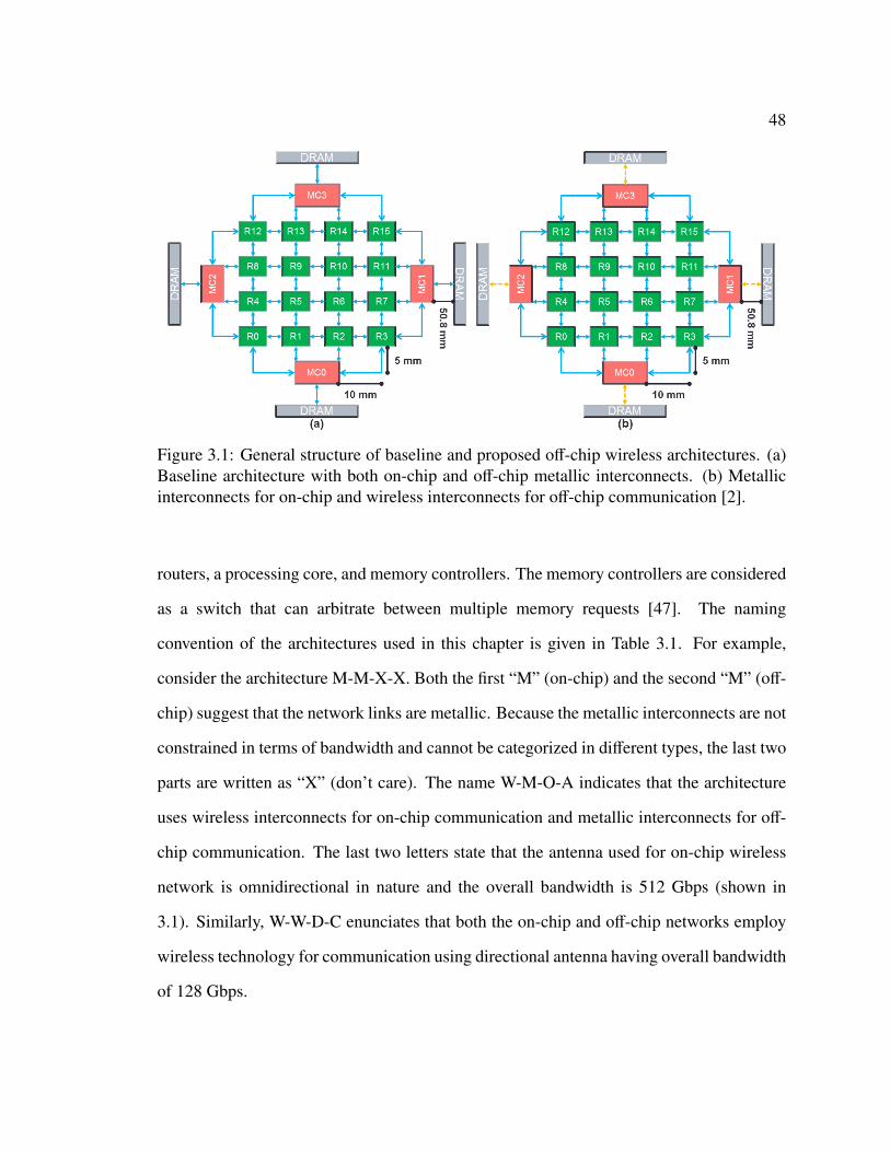
3.1 General structure of the baseline and proposed off-chip wireless architectures[2]. . . . . . . . . . . . . . . . . . . . . . . . . . . . . . . . . . . . . . . . . . 48
3.2 General structure of the proposed on-chip and off-chip wireless architectures [2]. 503.3 Communication mechanism of the proposed hybrid-wireless architectures [2]. . 55
4.1 Evaluation of OWN’s area requirement [1]© 2015 IEEE. . . . . . . . . . . . . 594.2 Evaluation of OWN’s energy requirement [1]© 2015 IEEE. . . . . . . . . . . 614.3 Evaluation of OWN’s latency requirement [1]© 2015 IEEE. . . . . . . . . . . 634.4 Evaluation of OWN’s saturation throughput [1]© 2015 IEEE. . . . . . . . . . 644.5 Evaluation of R-OWN’s area requirement. . . . . . . . . . . . . . . . . . . . . 654.6 Evaluation of R-OWN’s energy requirement. . . . . . . . . . . . . . . . . . . . 674.7 Evaluation of R-OWN’s latency requirement. . . . . . . . . . . . . . . . . . . 684.8 Evaluation of R-OWN’s saturation throughput. . . . . . . . . . . . . . . . . . 694.9 Execution time estimate of the hybrid-wireless architectures [2]. . . . . . . . . 724.10 Energy per byte comparison of the baseline and the proposed hybrid-wireless
architectures. . . . . . . . . . . . . . . . . . . . . . . . . . . . . . . . . . . . 73

10
List of AcronymsChip Multiprocessor CMPNetwork-on-Chip NoCOn-Chip Network OCNInstruction Level Parallelism ILPInstructions Per Cycle IPCDynamic Random Access Memory DRAMComplementary Metal Oxide Semiconductor CMOSMetal Oxide Field Effect Transistor MOSFETFin Field Effect Transistor FinFETTime Division Multiplexing TDMFrequency Division Multiplexing FDMCode Division Multiplexing CDMSpace Division Multiplexing SDMWavelength Division Multiplexing WDMDense Wavelength Division Multiplexing DWDMInternational Technology Roadmap for Semiconductors ITRSWireless Network-on-Chip WiNoCDimension Order Routing DORSingle-chip Cloud Computer SCCMulti-Purpose Processor Array MPPADynamic Voltage and Frequency Scaling DVFSSingle Write Multiple Read SWMRMultiple Write Single Read MWSRVirtual Channel VCGiga bit per second GbpsRadio Frequency RFMiss Status Hold Register MSHRMicro Ring Resonator MRRMicro Wireless Router MWRCarbon Nanotube CNTNetwork Interface Controller NICDouble Data Rate DDRLow Voltage Technology LVTUniform Normal UNBit Reversal BRPerfect Shuffle PSNeighbor NBRComplementary COMPMatrix Transpose MTButterfly BFLYPrinceton Application Repository for Shared-Memory Computers PARSEC
11
1 Introduction
In the last decade of the twentieth century, the performance of microprocessors,
following Moores law, continued to increase by using instruction level parallelism (ILP),
using faster clock frequency, and incrementing the number of transistors [9]. However, near
the beginning of the twenty-first century, as the processors issued multiple instructions
per cycle (IPC), marginal performance gains were achieved from ILP. Moreover, since
the dynamic power is directly proportional to frequency, the microprocessor clock
frequency could not be increased indefinitely. Thus, with the scaling down of transistors,
computer architects continued to add more transistors to achieve higher performance
gains. Nevertheless, the transistor power requirement was reduced with each process
generation, but accommodating a myriad number of transistors on a single chip increased
the total power consumption to a level where the chip and thermal management became
complex and insurmountable [10]. Therefore, the industry shifted from uniprocessor to
multiprocessor design, namely Chip Multiprocessor (CMP). As the name suggests, a CMP
is a collection of simple uniprocessors (processing core or simply core) integrated into
a single chip so that they can share the workload. As a result, a single, large complex
processor is replaced by several small simple processors to boost the performance [10].
The cores of a CMP may frequently need to communicate with each other to execute an
application or multiple applications. The simplest communication network in CMP is the
shared single bus that consists of a set of parallel wires to which various components are
connected. As the connected components share the bus, only one of them can transmit at a
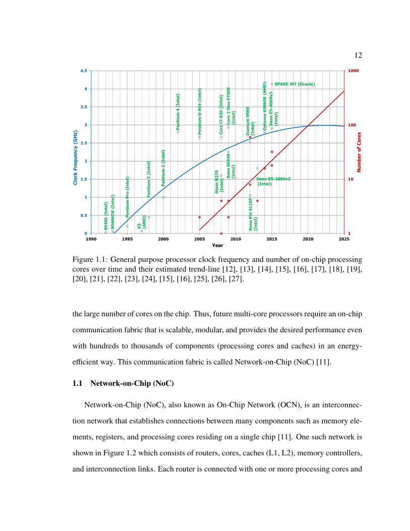
time which limits the performance and increases communication delay. In addition, Figure
1.1 shows that as the number of cores are exponentially increasing to satisfy application
requirements, a bus-based communication system is clearly not scalable to accommodate
0 Some material of this thesis was used verbatim from my publication [1] with permission© 2015 IEEEand two publications- [8] and [2] accepted but not published at the time of this thesis submission.
12
Figure 1.1: General purpose processor clock frequency and number of on-chip processingcores over time and their estimated trend-line [12], [13], [14], [15], [16], [17], [18], [19],[20], [21], [22], [23], [24], [15], [16], [25], [26], [27].
the large number of cores on the chip. Thus, future multi-core processors require an on-chip
communication fabric that is scalable, modular, and provides the desired performance even
with hundreds to thousands of components (processing cores and caches) in an energy-
efficient way. This communication fabric is called Network-on-Chip (NoC) [11].
1.1 Network-on-Chip (NoC)
Network-on-Chip (NoC), also known as On-Chip Network (OCN), is an interconnec-
tion network that establishes connections between many components such as memory ele-
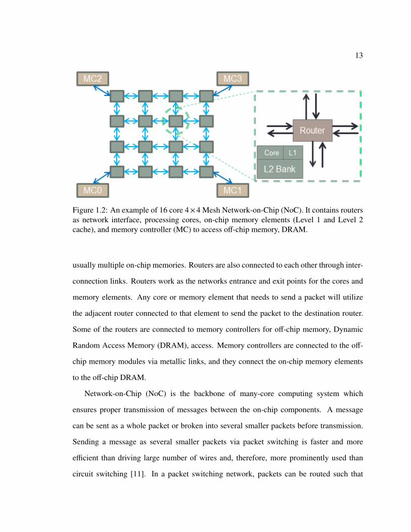
ments, registers, and processing cores residing on a single chip [11]. One such network is
shown in Figure 1.2 which consists of routers, cores, caches (L1, L2), memory controllers,
and interconnection links. Each router is connected with one or more processing cores and
13
Figure 1.2: An example of 16 core 4×4 Mesh Network-on-Chip (NoC). It contains routersas network interface, processing cores, on-chip memory elements (Level 1 and Level 2cache), and memory controller (MC) to access off-chip memory, DRAM.
usually multiple on-chip memories. Routers are also connected to each other through inter-
connection links. Routers work as the networks entrance and exit points for the cores and
memory elements. Any core or memory element that needs to send a packet will utilize
the adjacent router connected to that element to send the packet to the destination router.
Some of the routers are connected to memory controllers for off-chip memory, Dynamic
Random Access Memory (DRAM), access. Memory controllers are connected to the off-
chip memory modules via metallic links, and they connect the on-chip memory elements
to the off-chip DRAM.
Network-on-Chip (NoC) is the backbone of many-core computing system which
ensures proper transmission of messages between the on-chip components. A message
can be sent as a whole packet or broken into several smaller packets before transmission.
Sending a message as several smaller packets via packet switching is faster and more
efficient than driving large number of wires and, therefore, more prominently used than
circuit switching [11]. In a packet switching network, packets can be routed such that
14
the path requires least number of hops (minimal path) or is least congested (non-minimal
path) or a combination of both [11]. One popular routing method for the mesh network,
commonly used for NoCs and shown in Figure 1.2, is dimension order routing (DOR) [11].
Packets following DOR protocol may go in the X direction first, and then the Y direction
or vice versa to ensure a deadlock free routing. Since the mesh topology is easy to fabricate
and the DOR routing mechanism is easy to follow, DOR based mesh network is very
common. Some other common topologies include- torus, flatten butterfly, and concentrated
mesh [28]. Some of these topologies are shown below with several commercial processor
examples.
There are some commercial prototypes available that have implemented NoC as the
communication paradigm for many-core processors. For example, Intel Single-chip Cloud
Computer (SCC) has integrated 48 cores into a silicon chip and is intended to increase the
core counts to 100 and beyond. Intel SCC is divided into tiles where each tile contains
two cores, and the tiles are connected as a 2D mesh network [29]. Continuing the tile-
based approach, Intel Teraflops was presented which is the first programmable chip that
can compute one trillion mathematical calculations per second consuming only 62W. Intel
Teraflops contains 80 simple cores that are connected as a 2D mesh network [30]. Another
processor manufacturing company, EZchip, announced the first 100-core 64-bit processor
called Tile-Mx100. This processor uses ARMv8 core and a 2D mesh network to connect the
cores [31]. However, there are some drawbacks of a 2D mesh network such as congestion
at the center routers due to XY routing and large delay when the number of cores increases
due to additional hops. As a result, Kalray designed a MPPA (Multi-Purpose Processor
Array) with a 2D wrapped around torus NoC architecture, and the MPPA roadmap features
64 to 1024 cores on a single chip [32].
15
1.2 Issues in NoC
Traditional NoC designs are predominantly metallic 2D mesh or torus. With the
increasing number of cores, multi-hop communication and routing complexity increases
which significantly impacts the overall performance of the NoC due to high latency and
energy consumption [5]. In the following sub-sections the primary issues of NoC such as
energy, latency, and limitations of metallic interconnects are discussed.
1.2.1 Energy
The increase in the number of processing cores on a single chip has boosted the
network traffic which, in turn, has increased the energy consumption. Since higher
clock frequency increases energy dissipation, network clock frequency can be reduced
to lower the energy consumption. However, this would slow-down the communication
process and hurt performance. Instead of reducing the clock frequency, power-gating
can be used to reduce energy consumption by turning off the on-chip components not
being used. Nevertheless, power gating would incur additional delay due to the wake-
up latency of the turned-off on-chip components [33] [34]. Another technique for reducing
power consumption is Dynamic Voltage and Frequency Scaling (DVFS). DVFS adjusts
the interconnection bandwidth by varying the voltage and power levels, and thus, can
reduce the interconnection network energy dissipation [35]. Nonetheless, DVFS increases
the network cost due to the predictor and control circuits, the network complexity, and
incurs additional latency due to misprediction and switching. On the other hand, a routing
algorithm can play a role to constrain the energy consumption of a network. For example,
taking the minimal path would require less energy than the non-minimal path choices but
might congest some links. Therefore, proper selection of a routing algorithm is necessary
to mitigate the energy dissipation problem.
16
1.2.2 Latency
The increase of number of processing cores and memory intensive applications are
driving the network capacity to its limits and incrementing network congestion. Since
congestion can potentially stall the whole network, it is important to reduce network
congestion. One way to reduce network congestion is to increase network resources such as
channel width and number of buffers. Increasing these network resources would decrease
network congestion but increase the cost of the system. Hence, sharing of channels, buffers,
and links can be introduced to overcome the limited network resources and support the
network traffic demand. However, such sharing increases latency due to the delay in
shared network resource allocation. Another technique to speed up packet transmission,
and thus reduce latency, is flow control. Flow control techniques such as buffer allocation
and switch arbitration can be modified to improve latency, but this can increase network
and routing complexity. On the other hand, since network diameter is determined by the
routing algorithm used, the routing algorithm can play a vital role to reduce the network
latency. Nevertheless, both the minimal and non-minimal path routing can increase network
latency, depending on the network load pattern. Therefore, intelligent allocation of network
resources are necessary to keep the network latency a minimum.
1.2.3 Metallic Interconnects
Traditionally, metallic interconnection technology was used to connect the on-chip
components such as processing cores and memory controllers. Metallic interconnection
technology has the advantages of lower energy requirement, high bandwidth, and lower
area requirements. However, with the scaling down of the technology, wire resistance
and inter-wire capacitance are increasing which is increasing the energy consumption and
link latency. Additionally, increasing the number of cores requires multi-hop complex
routing that increases network latency. In order to facilitate lower latency communication,
17
one or more longer bus like links can be introduced, but this would contribute to the
increase of energy consumption and the number of repeaters. Moreover, according to
International Technology Roadmap for Semiconductor (ITRS), the development of metallic
interconnection technology would not be sufficient to satisfy the requirement of future
Chip Multiprocessors (CMPs). Therefore, as a potential solution to the problems faced
by metallic interconnection technology, researchers start to experiment with emerging
technologies such as wireless and photonics for interconnection networks.
1.3 Emerging Technologies in Interconnection Network: Wireless and Photonics
Emerging technologies such as wireless and photonics indicate promising outcomes
and have the potential to be the alternative of the traditional metallic interconnects. In light
of recent scholarly work on wireless and photonic interconnection networks, I will discuss
the advantages and disadvantages of these two technologies along with the architectures in
the following subsections.
1.3.1 Wireless Interconnection Network
Wireless technology offers several advantages such as one-hop communication, mul-
ticasting and broadcasting, reconfiguration of the network, absence of hardwired physical
channels, and Complementary Metal Oxide Semiconductor (CMOS) compatibility. How-
ever, Wireless technology is not energy efficient for short distance communication [36] [37]
and has a limited bandwidth at a 60 GHz center frequency. Additionally, the area footprint
of the wireless transceiver is higher compared to other interconnection technologies.
There are two types of Wireless Network-on-Chip (WiNoC): wireless-only and hybrid-
wireless. A wireless-only system utilizes wireless technology alone to connect the on-chip
components. Because of the limited bandwidth and high transceiver area, wireless-only
network is less common. In contrast, the hybrid-wireless system combines the short-range
metallic and wireless interconnects to communicate between the on-chip components. This
18
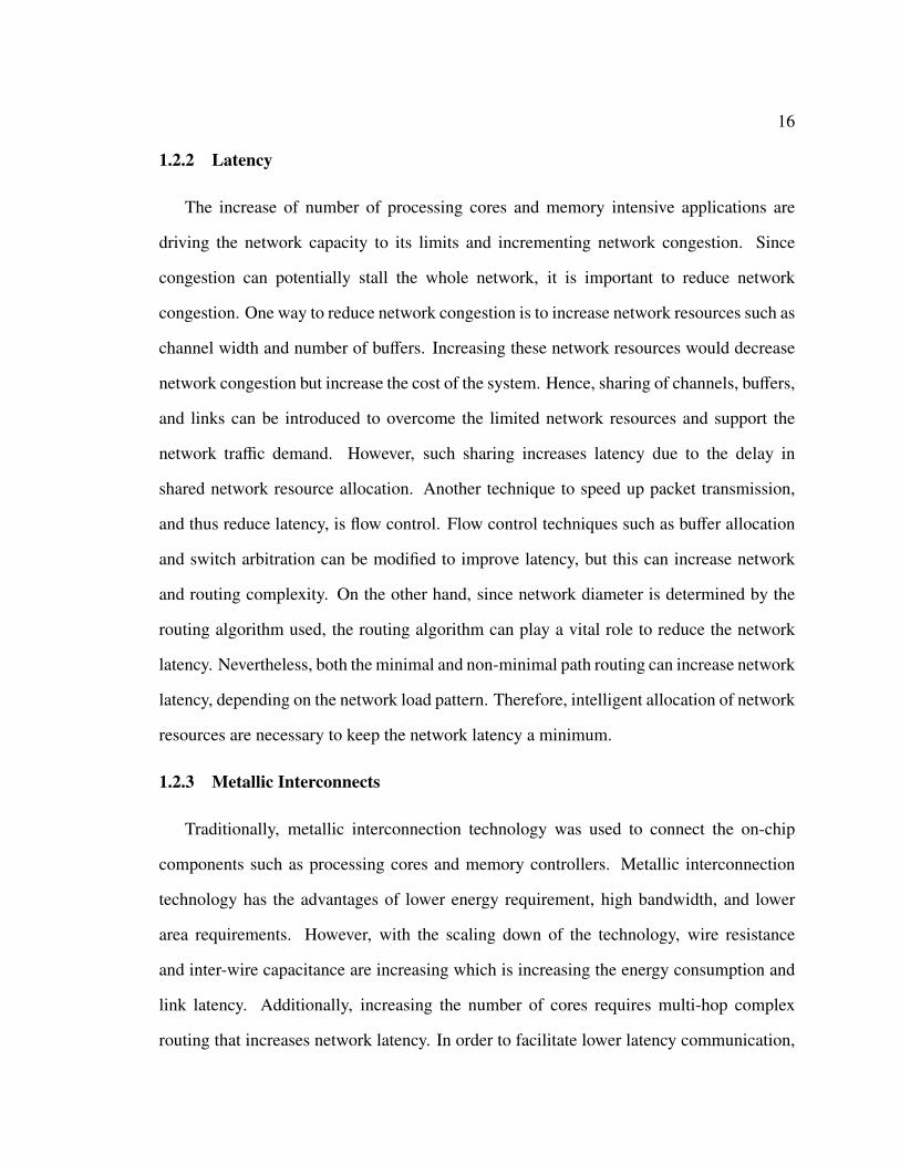
Figure 1.3: Layout of a WCube0 on the left and physical structure with addressing ofWCube on the right [3]© ACM DOI 10.1145/1614320.1614345.
system optimizes the usage of local metallic and wireless technology to reduce latency
and energy consumption of the network, and thus, is more common. The bandwidth
limitation of on-chip wireless technology can be circumvented by employing time division
multiplexing (TDM), frequency division multiplexing (FDM), space division multiplexing
(SDM), and code division multiplexing (CDM) techniques. Therefore, most of the hybrid-
wireless networks use a combination of these techniques. One such network is WCube
[3], shown in Figure 1.3. WCube is built on top of CMesh [28] by inserting a micro
wireless router (MWR) for every 64-core cluster. MWR is used to transmit a packet if
the number of wired hops required is higher than the number of wireless hops required.
This network scales logarithmically with the number of cores and provides a lower-latency
and energy-efficient network by optimizing metallic and wireless technologies. However,
WCube is a multi-hop wireless network which does not utilize the advantage of one-hop
wireless transmission, and the wireless hops required increases proportionally with the
level of WCube. Moreover, source WCube overhears its own message due to the nature
of transmission which increases energy consumption. In addition, the number of receivers
required increases multiplicatively with the level of WCube, and the frequency spectrum is
19
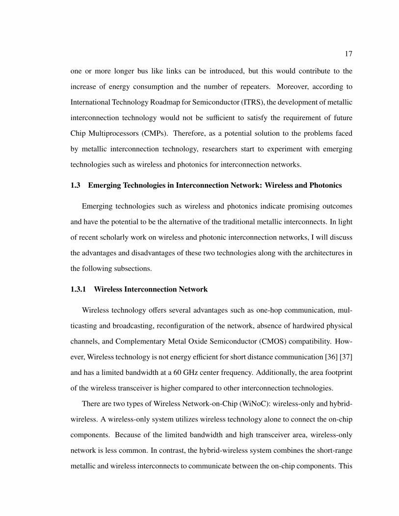
Figure 1.4: (a) Subnet architecture and network topology of hubs connected by asmall-world graph [4]. © 2011 IEEE (b) iWISE-256 architecture showing the wirelesscommunication between sets [5]© 2011 IEEE.
not reusable. WiNoC [4] proposes a two-tier hybrid wireless architecture where cores are
divided into subnets and subnets are connected using wired and wireless links, shown in
Figure 1.4 (a). All the cores of a subnet are connected to a hub, and hubs use wired links
to communicate with the neighboring hubs and wireless links for distant hubs. However,
the primary disadvantage of WiNoC is that the CNT antenna used is difficult to fabricate
and a long wire is required to connect the hub with the cores. Moreover, the architecture is
not scalable because increasing the subnet size decreases throughput and increases energy
dissipation per packet as well as area of the network.
iWISE [5] distributes the wireless hubs throughout the network as shown in Figure
1.4 (b). It provides one hop communication between any two cores either using a
wired or wireless link for a 64-core network. It uses a combination of TDM and
FDM to scale to a higher number of cores. It reduces energy consumption and area
requirement with improved performance when compared to other state-of-the-art metallic
and wireless architectures. Nevertheless, the main disadvantage of iWISE is that scalability
becomes expensive and complex. HCWiNoC, another hybrid wireless architecture with
20
distributed hubs, can scale up to kilo-core and double the throughput with a reduced energy
requirement when compared to other state-of-the-art WiNoC architecture [38]. However,
the area cost of this network is high.
1.3.2 Photonic Interconnection Network
Photonic technology includes the advantages of high bandwidth, lower power
requirement, low latency, convenient reconfiguration of the network, multicasting and
broadcasting, and CMOS compatibility. However, Photonic technology requires a physical
waveguide(s) that defines the network connection and optical-only crossbars are not
scalable to kilo-core networks [1]. In addition, this technology involves inefficient off-chip
laser source coupling, static laser power loss, electrical to optical and optical to electrical
conversion loss, and high broadcasting power [6].
Similar to wireless network, photonic network can be of two types: (1) photonic-
only network uses only photonics to facilitate on-chip communication whereas (2) hybrid-
photonic network uses wired link in addition to photonic link for transmission of packets.
Early photonic networks generally use global photonic crossbar with wavelength division
multiplexing (WDM). One such network is Corona presented in [39]. Corona proposes
a photonic crossbar for a 256-core network with core concentration of 4 which provides
one-hop communication between any two cores. Each waveguide contains 64 wavelengths
with an off-chip laser source. Each router is connected to a memory controller through
a photonic link and to an arbitration waveguide to maintain signal integrity. Corona uses
single-write-multiple-read (SWMR) arbitration technique where a router sends messages
to its assigned wavelengths. This message can be read by all other routers of the network.
However, Corona requires laser power proportional to the number of detectors and is not
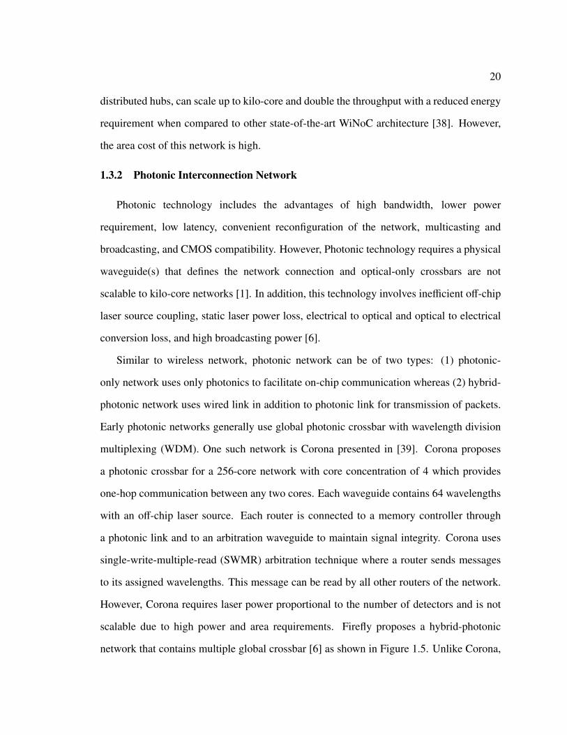
scalable due to high power and area requirements. Firefly proposes a hybrid-photonic
network that contains multiple global crossbar [6] as shown in Figure 1.5. Unlike Corona,
21
Figure 1.5: Shared waveguide inter-cluster communication is shown on the left andwaveguide for a 256-core architecture is shown on the right [6] © ACM DOI10.1145/1555754.1555808.
in order to reduce broadcasting power, Firefly uses reservation-assisted SWMR (R-SWMR)
where electrical links are used to turn on the destination detector only. It also divides
the network into several smaller clusters. Intra-cluster communication employs electrical
link whereas inter-cluster communication uses multiple photonic crossbars with dense
wavelength division multiplexing (DWDM). The use of multiple smaller crossbars reduces
the hardware complexity and excludes the need of global arbitration. However, the R-
SWMR introduces area and energy overhead, and multiple global link traversals increases
conversion loss and transmission power.
A photonic Clos based network is proposed in [40] that shows improved performance
compared to a global photonic crossbar. It consumes lower energy and area due to
small diameter crossbar network and provides uniform throughput and latency. It is
an optimization of low-radix, high-diameter mesh and high-radix low-diameter crossbar
topology. It requires shorter waveguides with lesser number of rings and provides
22
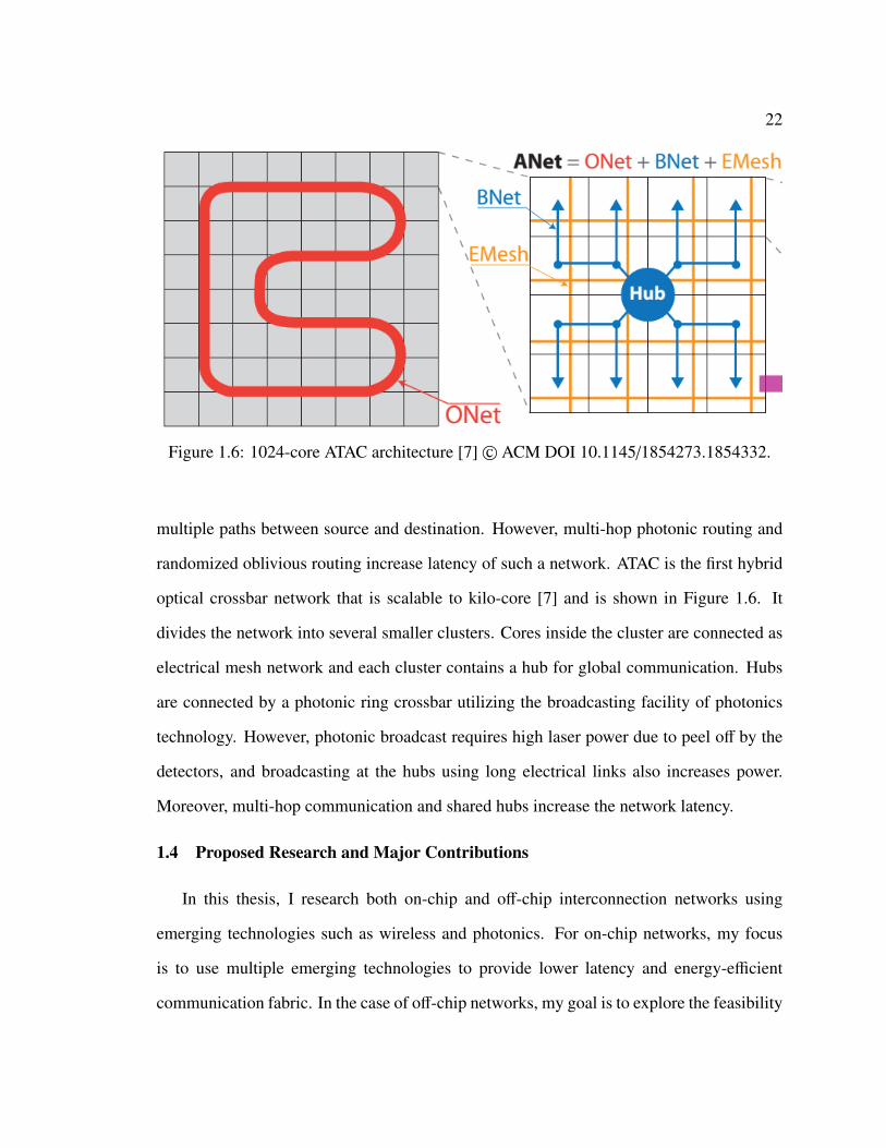
Figure 1.6: 1024-core ATAC architecture [7]© ACM DOI 10.1145/1854273.1854332.
multiple paths between source and destination. However, multi-hop photonic routing and
randomized oblivious routing increase latency of such a network. ATAC is the first hybrid
optical crossbar network that is scalable to kilo-core [7] and is shown in Figure 1.6. It
divides the network into several smaller clusters. Cores inside the cluster are connected as
electrical mesh network and each cluster contains a hub for global communication. Hubs
are connected by a photonic ring crossbar utilizing the broadcasting facility of photonics
technology. However, photonic broadcast requires high laser power due to peel off by the
detectors, and broadcasting at the hubs using long electrical links also increases power.
Moreover, multi-hop communication and shared hubs increase the network latency.
1.4 Proposed Research and Major Contributions
In this thesis, I research both on-chip and off-chip interconnection networks using
emerging technologies such as wireless and photonics. For on-chip networks, my focus
is to use multiple emerging technologies to provide lower latency and energy-efficient
communication fabric. In the case of off-chip networks, my goal is to explore the feasibility

23
of using emerging technologies as an alternative to the current metallic technology. In the
following subsections, I will discuss these research objectives in detail.
1.4.1 Heterogeneity in Interconnection Network
Emerging technologies are expected to be the future alternative of the traditional
metallic interconnection technology, but as discussed, emerging technologies have
drawbacks similar to metallic interconnection technology. As a result, hybrid networks
are introduced where traditional metallic technology and emerging technologies coexisted
on the same architecture. However, the demands of faster computing machines will exceed
the capacity of the hybrid architectures in the near future. Thus, one emerging technology is
not sufficient, and it is necessary to exploit the benefits of multiple emerging technologies
to provide the desired performance. This integration of multiple emerging technologies
into an interconnection network is called heterogeneity in interconnection network.
In this thesis, I propose to integrate two emerging technologies, photonics and wireless,
on the same chip. Wireless and photonic technologies have the potential to complement
each other in order to boost energy savings and performance gains that cannot be achieved
with a single technology. First, wireless technology is constrained in bandwidth; whereas,
photonics has ample bandwidth. Second, where photonic link requires the presence of
physical waveguide, wireless does not require any hard-wired channel. Third, while
photonic power consumption increases with the increase of waveguide length, wireless
technology is more efficient for distant communication. Fourth, wireless transceiver
footprint is higher compared to other technologies, and smaller photonic crossbar is
area efficient. Therefore, the combination of photonic and wireless technology in an
interconnection network could be promising. My simulation results show that the
proposed heterogeneous architecture consumes 30% less energy/bit than wireless and 14%
more energy/bit than photonic architecture while providing higher saturation throughput
24
when compared to wired, wireless, and photonic networks. In addition, the proposed
heterogeneous architecture occupies 34% more and 35% less area than hybrid-wireless
and photonic-only architectures respectively.
1.4.2 Off-Chip Interconnection Network
Even though the importance of the on-chip communication paradigm cannot be denied,
the off-chip memory access latency also cannot be ignored anymore due to the increase
in off-chip memory accesses. As a result, the industry, currently, is focusing not only on
on-chip latency and energy cost reduction, but also on ways to reduce the off-chip memory
access latency and energy cost. Therefore, emerging technology such as wireless is being
considered to reduce off-chip memory access latency and energy.
The energy cost of the metallic technology increases proportionally with distance.
Since the distance between a memory controller and a DRAM is large (around 50mm
[41]) compared to the on-chip distances (around 5mm), wireless technology can be a better
alternative. Moreover, wireless technology can provide flexible interconnection between
several distant memory modules which becomes complex if metallic technology is used.
For example, memory controllers may need to communicate with each other. This can
be achieved in wireless technology by allocating a unique or shared frequency channel.
In contrast, long wires are required if metallic technology is used. In addition, off-chip
link traversal time for wireless technology is lower compared to the metallic technology.
This is because the metallic technology requires repeaters which introduce RC delay.
My simulation results show that the proposed hybrid-wireless architectures consume on
average 79% less energy per byte with 11% lower execution time when compared to the
baseline wired architectures.
25
1.4.3 Key Contributions and Thesis Organization
In the preceding sub-sections of this section, I described the research focus of this thesis
and presented my main ideas. The major contributions of this thesis are the following:
• Exploration of heterogeneity in interconnection network: The idea of combining
wireless and photonic technologies on the same chip has some technological
limitations. In this thesis, I not only analyze the use of these two technologies on the
same chip in terms of performance but also elaborate on the technological feasibility
of combining them.
• Introduction of reconfigurable links in a heterogeneous network: In addition to the
introduction of the heterogeneous network, I optimized the wireless link usage by
reconfiguring the wireless links at run-time. My simulation results indicate that
the reconfigurable heterogeneous architecture improves the performance (throughput
and latency) by 15% when compared to the baseline heterogeneous architecture.
However, the energy consumption of the reconfigurable heterogeneous architecture
is 7% higher than the baseline heterogeneous architecture for a 256-core network.
• Emerging technologies for off-chip network: Emerging technologies might be the
future alternative to metallic links for off-chip memory access. I explore the use of
wireless technology for the first time to access off-chip memory, DRAM.
The rest of the thesis is organized as follows: chapter two describes the proposed
heterogeneous and reconfigurable heterogeneous architectures with technological aspects,
chapter three delineates the use of wireless technology for off-chip memory access, chapter
four presents the simulation results of the networks proposed in chapter two and three, and
chapter five concludes the thesis.
26
2 Heterogeneous Network-on-Chip
In this chapter, I discuss the two proposed architectures: Optical and Wireless Network-
on-Chip (OWN) architecture for 1024-core CMPs and Reconfigurable Optical and Wireless
Network-on-Chip (R-OWN) architecture for 256-core CMPs. Both architectures combine
the optical and wireless technologies to provide a scalable, low latency, and energy efficient
network-on-chip. I propose to share an optical crossbar by 64 cores (called a cluster) using
wavelength division multiplexing (WDM) technique because this decomposition of optical
crossbars allows to (1) maximize the efficiency of lasers since the lasers are always on, (2)
reduce latency by reducing the wait time for tokens, and (3) reduce insertion losses due to
shorter waveguides. I also propose to use wireless technology to interconnect the clusters
in order to provide one-hop cluster-to-cluster communications [1].
Instead of using wireless interconnects, a second level of metallic or optical
interconnects could be used to connect the clusters, but there would be several
complications. Two complications that can occur with metallic interconnects are: (1) a
metallic interconnect would not scale for a higher number of cores (say, 1024-cores) and
(2) reconfiguring a metallic interconnect-for example, using power gating-would increase
network complexity. Three complications may occur for optical interconnects: (1) multiple
optical layers would cause heat dissipation problem that could deteriorate the network
performance because optics is sensitive to heat, (2) optical networks would require constant
laser power and turning off certain wavelengths would require off-chip transmission which
would incur additional delay, and (3) a higher number of modulators and demodulators
would be required for reconfiguration which would increase power loss. In contrast,
wireless interconnects are ideal for reallocating bandwidth due to the lack of wires and
wide frequency spectrum, and since the antennas are on the chip, they can be turned off if
necessary. As a result, I can build an architecture up to 1024-cores that requires a maximum
of three hops for any-to-any core communication.
27
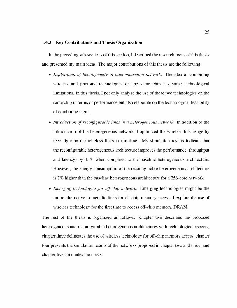
Figure 2.1: 64-core OWN architecture consisting of a 16 × 16 optical crossbar, datawaveguide(s), and an arbitration waveguide. The structure of a tile and the proposed opticalrouter is shown on the right.
This chapter is organized in three sections. First, I describe in detail the architecture
of OWN with the routing mechanism and deadlock avoidance technique. Second, I
evaluate the technological feasibility of implementing OWN. Third, I build R-OWN on
top of OWN by making the wireless links reconfigurable at runtime to incorporate diverse
communication patterns and describe a deadlock free routing mechanism which is different
from OWN.
2.1 OWN Architecture
In this section, first, I describe the design of a 64-core OWN architecture using optical
technology. Second, I use the 64-core OWN as the basic building block to design a 1024-
core OWN employing wireless technology. Third, I explain the routing mechanism with
examples. Fourth, since the switching of technology (optical to wireless and wireless to
28
optical) may create deadlocks, I propose a technique to ensure deadlock freedom [1] ©
2011 IEEE.
2.1.1 64-Core OWN Architecture: Cluster
The OWN architecture is a tile-based architecture with each tile consisting of four
processing cores and their private L1 instruction and data caches, a shared L2 cache, and
a network interface controller (NIC) or router. The inner components of a tile are shown
in Figure 2.1 for the four cores connected to router 15 (upper right-most tile). Each tile is
located within a cluster, which consists of 16 such tiles (64 cores). The tiles inside a cluster
are represented by two coordinates (r, c) where r is the number of the tile or the router and
c identifies one of the four cores in that tile. These tiles are connected by a 16 × 16 optical
crossbar which is the snake-like optical waveguide and takes one hop for core-to-core
communication, as shown in Figure 2.1. I propose a multiple-write-single-read (MWSR)
scheme with arbitration wherein each tile is assigned dedicated wavelength(s) to receive
messages from the remaining 15 tiles. In contrast, a single-write-multiple-read (SWMR)
scheme requires high laser power because one router writes to its assigned channel and
all the remaining routers can read by peeling off a portion of the wavelengths[6]. I
chose MWSR over SWMR to reduce the laser power consumption; however, the power
consumption can be reduced even in SWMR by tuning only the intended receiver [6].
The tradeoff in using MWSR is increased latency since each router must wait to grab the
token before writing to a specific channel. As there are 16 routers inside the cluster and
communication between the routers requires only one hop, I argue that this latency will not
dramatically affect the performance. Hence, any one of the 15 tiles of the 64-core OWN
architecture can write to the other tiles such that all 16 tiles can read at the same time in
their assigned wavelength(s). Thus, each cluster requires two waveguides. For example,
core (1, 3) wants to send a packet to core (5, 2). Router 1 will wait for the token to modulate
29
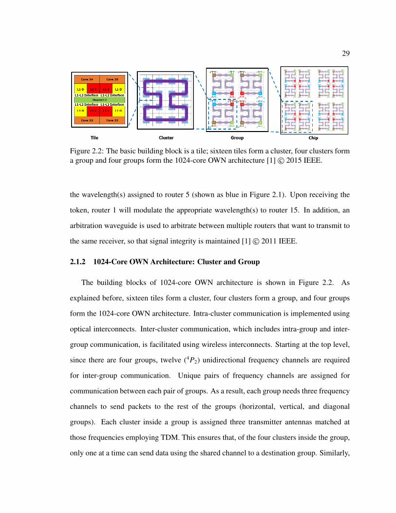
Figure 2.2: The basic building block is a tile; sixteen tiles form a cluster, four clusters forma group and four groups form the 1024-core OWN architecture [1]© 2015 IEEE.
the wavelength(s) assigned to router 5 (shown as blue in Figure 2.1). Upon receiving the
token, router 1 will modulate the appropriate wavelength(s) to router 15. In addition, an
arbitration waveguide is used to arbitrate between multiple routers that want to transmit to
the same receiver, so that signal integrity is maintained [1]© 2011 IEEE.
2.1.2 1024-Core OWN Architecture: Cluster and Group
The building blocks of 1024-core OWN architecture is shown in Figure 2.2. As
explained before, sixteen tiles form a cluster, four clusters form a group, and four groups
form the 1024-core OWN architecture. Intra-cluster communication is implemented using
optical interconnects. Inter-cluster communication, which includes intra-group and inter-
group communication, is facilitated using wireless interconnects. Starting at the top level,
since there are four groups, twelve (4P2) unidirectional frequency channels are required
for inter-group communication. Unique pairs of frequency channels are assigned for
communication between each pair of groups. As a result, each group needs three frequency
channels to send packets to the rest of the groups (horizontal, vertical, and diagonal
groups). Each cluster inside a group is assigned three transmitter antennas matched at
those frequencies employing TDM. This ensures that, of the four clusters inside the group,
only one at a time can send data using the shared channel to a destination group. Similarly,
30
each cluster has three receiver antennas tuned at the frequencies of other groups. Since I
use multicast to overcome wireless bandwidth limitation, receivers of all four clusters can
receive messages or packets at the same time. However, each cluster decides whether to
keep or discard the packet(s). Inside a group, the four clusters are connected using a 32
Gbps frequency channel. This frequency channel is shared by the four clusters of a group
where only one of them can write but all of them can receive simultaneously. Therefore,
each cluster of a group will have four transceivers: one for intra-group communication and
three for inter-group communication [1]© 2011 IEEE.
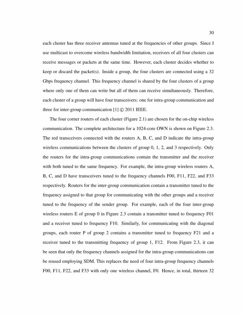
The four corner routers of each cluster (Figure 2.1) are chosen for the on-chip wireless
communication. The complete architecture for a 1024-core OWN is shown on Figure 2.3.
The red transceivers connected with the routers A, B, C, and D indicate the intra-group
wireless communications between the clusters of group 0, 1, 2, and 3 respectively. Only
the routers for the intra-group communications contain the transmitter and the receiver
with both tuned to the same frequency. For example, the intra-group wireless routers A,
B, C, and D have transceivers tuned to the frequency channels F00, F11, F22, and F33
respectively. Routers for the inter-group communication contain a transmitter tuned to the
frequency assigned to that group for communicating with the other groups and a receiver
tuned to the frequency of the sender group. For example, each of the four inter-group
wireless routers E of group 0 in Figure 2.3 contain a transmitter tuned to frequency F01
and a receiver tuned to frequency F10. Similarly, for communicating with the diagonal
groups, each router P of group 2 contains a transmitter tuned to frequency F21 and a
receiver tuned to the transmitting frequency of group 1, F12. From Figure 2.3, it can
be seen that only the frequency channels assigned for the intra-group communications can
be reused employing SDM. This replaces the need of four intra-group frequency channels
F00, F11, F22, and F33 with only one wireless channel, F0. Hence, in total, thirteen 32
31
Figure 2.3: Kilo-core OWN architecture. Routers with the same letter share a frequencychannel and Fxy represent a wireless channel to send packets from group x to group y. Forexample, Routers A, B, C, and D share the intra-group wireless channel F00, F11, F22, andF33 respectively. Routers E, F, G, and H require four inter-group wireless channels F01,F10, F23, and F32 respectively to communicate with the horizontal group. Routers I, J,K, and L require four inter-group wireless channels F02, F20, F13, and F31 respectivelyto communicate with the vertical group. Routers M, N, O, and P require four inter-groupwireless channels F03, F30, F12, and F21 respectively to communicate with the diagonalgroup [1]© 2015 IEEE.
32
Gbps frequency channels are required for the proposed OWN architecture. More on this
wireless technology is explained in the technology section [1]© 2011 IEEE.
2.1.3 Intra-Group and Inter-Group Communication
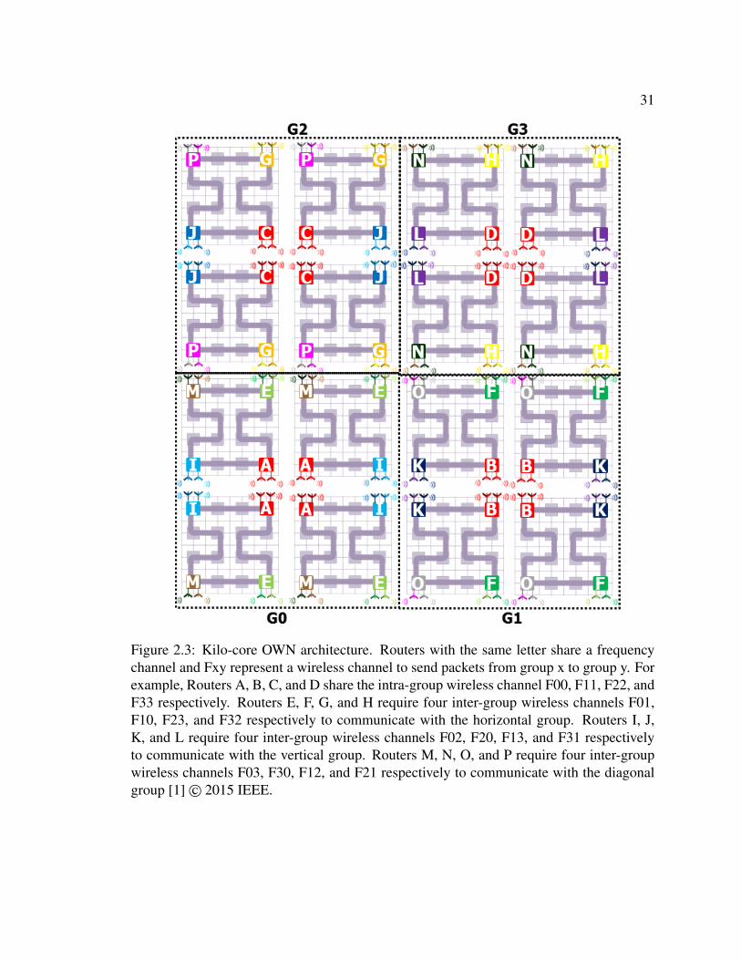
Consider Figure 2.4 for the detailed communication pattern. Each core in 1024-core
OWN is identified by a 4-digit coordinate with group, cluster, router, and core number. It
is represented as (g, cs, r, c) where g is group, cs is cluster, r is router, and c is core number.
Thus, the total number of cores in OWN is g × cs × r × c, where 0 ≤ g ≤ 3, 0 ≤ cs ≤ 3,
0 ≤ r ≤ 15, and 0 ≤ c ≤ 3. For example, core (2, 2, 0, 1) is in group 2, cluster 2 (top-left
position inside a group), and at the first tile (router 0). If this core wants to send a packet
to core (2, 1, 13, 3), then it is an intra-group communication. The packet from the source
router will be sent to the right-most corner router (2, 2, 3) using optical link when it has
the token to write. Once the packet arrives at the router (2, 2, 3), the router will wait for
the intra-group frequency channel, F0. Once router (2, 2, 3) has the right to transmit, it will
broadcast the packet to the other three routers that are assigned the intra-group wireless
frequency. Only the router (2, 1, 12) at the destination cluster will accept the packet, and
the remaining two routers will discard the packet. When router (2, 1, 12) has the token to
write to the wavelengths assigned to router (2, 1, 13), router (2, 1, 12) will send the packet
to the destination router (2, 1, 13) over the optical link. This will require three hops in the
following sequence: one optical, one wireless, and one optical [1]© 2011 IEEE.
Let me consider inter-group wireless communication between horizontal groups with
source core (2, 3, 14, 3) and destination core (3, 2, 11, 1). The source core (2, 3, 14, 3) will
insert the packet to the router (2, 3, 14). After receiving the token, this router will send the
packet to router (2, 3, 15) using optical link. Router (2, 3, 15) will contend for the wireless
channel F23 with the three other routers (shown as G in Figure 2.4) in that group. Once
it has permission to use the channel F23, the packet will be broadcasted to all four routers
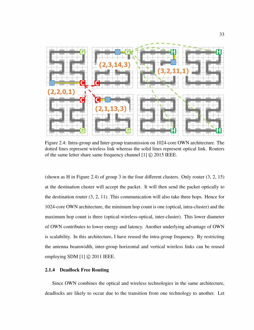
33
Figure 2.4: Intra-group and Inter-group transmission on 1024-core OWN architecture. Thedotted lines represent wireless link whereas the solid lines represent optical link. Routersof the same letter share same frequency channel [1]© 2015 IEEE.
(shown as H in Figure 2.4) of group 3 in the four different clusters. Only router (3, 2, 15)
at the destination cluster will accept the packet. It will then send the packet optically to
the destination router (3, 2, 11). This communication will also take three hops. Hence for
1024-core OWN architecture, the minimum hop count is one (optical, intra-cluster) and the
maximum hop count is three (optical-wireless-optical, inter-cluster). This lower diameter
of OWN contributes to lower energy and latency. Another underlying advantage of OWN
is scalability. In this architecture, I have reused the intra-group frequency. By restricting
the antenna beamwidth, inter-group horizontal and vertical wireless links can be reused
employing SDM [1]© 2011 IEEE.
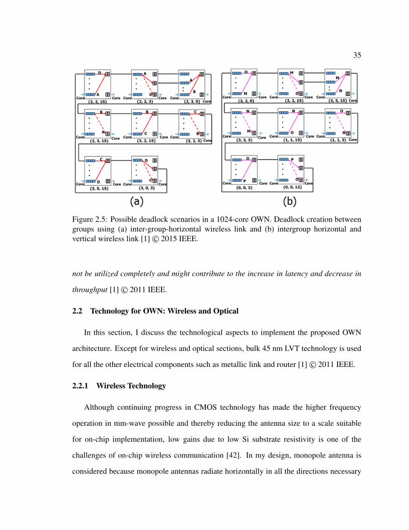
2.1.4 Deadlock Free Routing
Since OWN combines the optical and wireless technologies in the same architecture,
deadlocks are likely to occur due to the transition from one technology to another. Let
34
us consider Figure 2.5 (a). It shows four packets A, B, C, and D where A and C are
intra-group and B and D are inter-group packets. Packet A originates at router (2, 2, 15),
takes the optical link to router (2, 2, 3), reaches intra-group wireless-network-router (2, 3,
0), and then arrives at the destination router (2, 3, 15) via optical link where it exits the
network. Similarly, the travel path of packet C is: router (3, 2, 15)-optical link-router (3,
2, 3)-intra-group wireless link-router (3, 0, 15)-optical link-router (3, 0, 3). Inter-group
packet B originates at router (2, 3, 0), via optical link reaches router (2, 3, 15), takes inter-
group-horizontal wireless link to router (3, 2, 15), and then arrives at the destination router
(3, 2, 3) via optical link where it exits the network. Similarly, the travel path of the other
inter-group packet D is: router (3, 0, 15)-optical link-router (3, 0, 3)-inter-group horizontal
wireless link-router (2, 2, 15)-optical link-router (2, 2, 3). All the packets require three
hops to reach their respective destination router from the source router. Either A, C or
B, D alone do not create any deadlock, but simultaneous transmission of A, B, C, and D
creates circular dependency. Another case of deadlock that includes inter-group vertical
and horizontal wireless communication with intra-group wireless communication is shown
on Figure 2.5 (b) [1]© 2011 IEEE.
There are different types of deadlock avoidance techniques such as distance class or
dateline class [11]. To avoid deadlocks in OWN architecture, I have followed a form of
dateline class. Each router of OWN has 4 virtual channels (VCs) associated with each
input port. I restrict the VC allocation for each type of communication. Both intra-cluster
and intra-group transmissions use VC0 only. The rest of the VCs-VC1, VC2, and VC3 are
assigned to the flits requiring inter-group horizontal, vertical, and diagonal transmissions
respectively. These VC assignments are followed throughout the lifetime of the packet in
the network. This proposed deadlock avoidance technique ensures that all packets reach
their intended destinations. However, due to this restricted VC allocation, input buffers will
35
Figure 2.5: Possible deadlock scenarios in a 1024-core OWN. Deadlock creation betweengroups using (a) inter-group-horizontal wireless link and (b) intergroup horizontal andvertical wireless link [1]© 2015 IEEE.
not be utilized completely and might contribute to the increase in latency and decrease in
throughput [1]© 2011 IEEE.
2.2 Technology for OWN: Wireless and Optical
In this section, I discuss the technological aspects to implement the proposed OWN
architecture. Except for wireless and optical sections, bulk 45 nm LVT technology is used
for all the other electrical components such as metallic link and router [1]© 2011 IEEE.
2.2.1 Wireless Technology
Although continuing progress in CMOS technology has made the higher frequency
operation in mm-wave possible and thereby reducing the antenna size to a scale suitable
for on-chip implementation, low gains due to low Si substrate resistivity is one of the
challenges of on-chip wireless communication [42]. In my design, monopole antenna is
considered because monopole antennas radiate horizontally in all the directions necessary
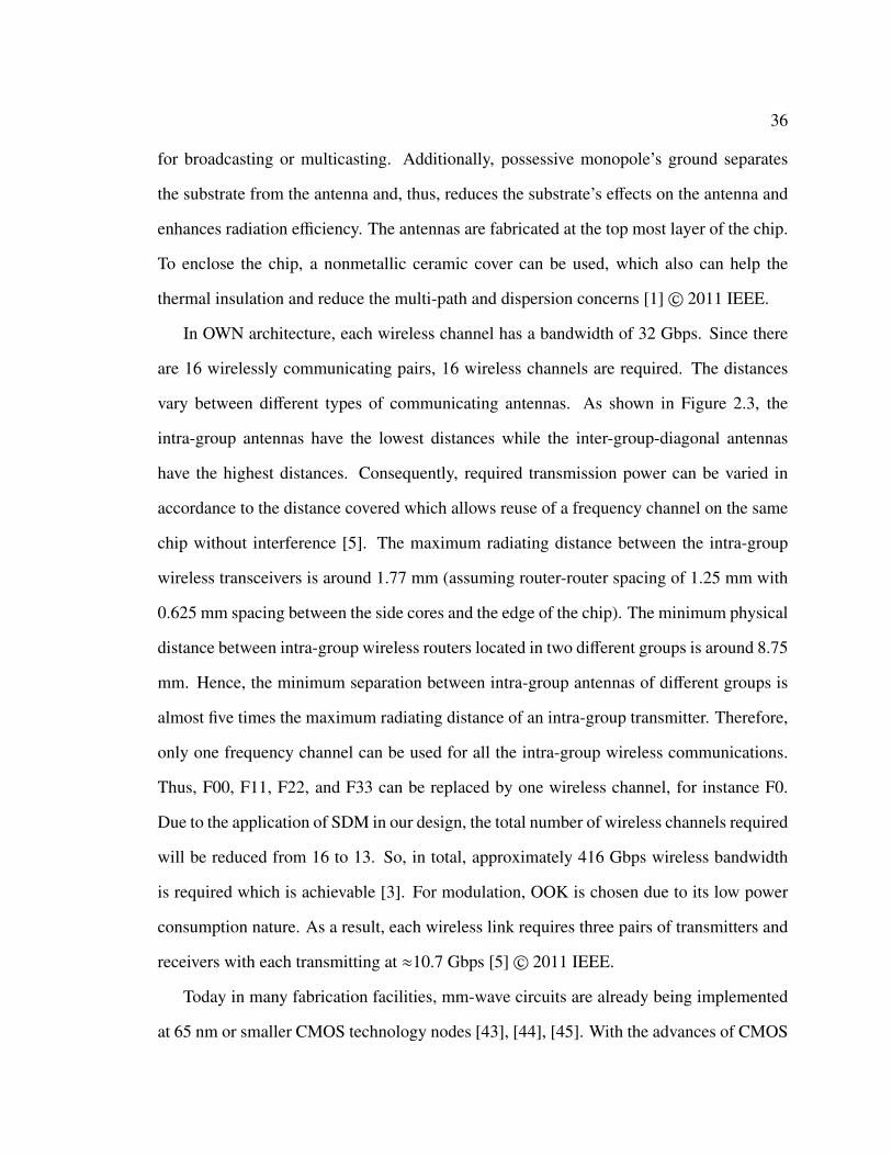
36
for broadcasting or multicasting. Additionally, possessive monopole’s ground separates
the substrate from the antenna and, thus, reduces the substrate’s effects on the antenna and
enhances radiation efficiency. The antennas are fabricated at the top most layer of the chip.
To enclose the chip, a nonmetallic ceramic cover can be used, which also can help the
thermal insulation and reduce the multi-path and dispersion concerns [1]© 2011 IEEE.
In OWN architecture, each wireless channel has a bandwidth of 32 Gbps. Since there
are 16 wirelessly communicating pairs, 16 wireless channels are required. The distances
vary between different types of communicating antennas. As shown in Figure 2.3, the
intra-group antennas have the lowest distances while the inter-group-diagonal antennas
have the highest distances. Consequently, required transmission power can be varied in
accordance to the distance covered which allows reuse of a frequency channel on the same
chip without interference [5]. The maximum radiating distance between the intra-group
wireless transceivers is around 1.77 mm (assuming router-router spacing of 1.25 mm with
0.625 mm spacing between the side cores and the edge of the chip). The minimum physical
distance between intra-group wireless routers located in two different groups is around 8.75
mm. Hence, the minimum separation between intra-group antennas of different groups is
almost five times the maximum radiating distance of an intra-group transmitter. Therefore,
only one frequency channel can be used for all the intra-group wireless communications.
Thus, F00, F11, F22, and F33 can be replaced by one wireless channel, for instance F0.
Due to the application of SDM in our design, the total number of wireless channels required
will be reduced from 16 to 13. So, in total, approximately 416 Gbps wireless bandwidth
is required which is achievable [3]. For modulation, OOK is chosen due to its low power
consumption nature. As a result, each wireless link requires three pairs of transmitters and
receivers with each transmitting at ≈10.7 Gbps [5]© 2011 IEEE.
Today in many fabrication facilities, mm-wave circuits are already being implemented
at 65 nm or smaller CMOS technology nodes [43], [44], [45]. With the advances of CMOS
37
Table 2.1: Optical device parameters [1]© 2015 IEEE.
Parameter Value Parameter Value
Waveguide Pitch 4 µm Ring Resonator Diam-
eter
12 µm
Wavelengths/Waveguide 64 Waveguide Loss 1.0 dB/cm
Pass-by Ring Resonator Loss 0.0001 dB Photo-detector Loss 1.0 dB
Splitter Loss 0.2 dB Modulation Loss 1.0 dB
Demodulation Loss 1.0 dB Receiver Sensitivity -17 dBm
Laser Efficiency 15% Ring Heating Power 26 µW/ring
Ring Modulating Power 500
µW/ring
Ring Modulation Fre-
quency
10 GHz
technology and scaling, higher frequency of operation with lower power requirement may
be possible. Based on the current trends in fabrication, wireless link power efficiency could
possibly reach about 1 pJ/bit [37]. Moreover, application of the double-gate MOSFETs
(FinFETs) may lower the threshold voltage of the transistor which will help to reduce
the supply voltage and, as a result, power dissipation. Additionally, a power reduction
of three times and lower losses in ultra-thin Si devices may be projected for RF wireless
transceivers built using 22 nm technology, thanks to smaller passives and improvements
in nano-materials and transistor off-currents. With this admittedly optimistic outlook, I
believe it is possible to reach and even drop below 1pJ/bit energy efficiency for wireless
links to be used in OWN implementation [1]© 2011 IEEE.
2.2.2 Photonics Technology
Optical transmission requires the presence of optical waveguide and ring modulators.
Each waveguide can contain up to 64 wavelengths. My proposed architecture OWN
38
applies WDM to communicate via the optical waveguide. The modulators can modulate
the wavelengths at 10 Gbps using electro-modulation [46]. Since except for the optical
waveguide all the on-chip components are electrical in nature, I need electrical-to-optical
and optical-to-electrical converters at both sides of the optical transmission line. To
convert the electrical signal to optical signal, photodiodes can be used and to convert the
optical signal to electrical signal, photodetectors and cascaded amplifiers can be used. The
technological parameters used in this thesis for optical links are shown in Table 2.1 [1] ©
2011 IEEE.
2.3 Reconfigurable-OWN (R-OWN)
In this section, first, I briefly explain the 256-core OWN architecture. Second, I describe
the design of R-OWN for 256 cores and describe the wireless channel reconfiguration.
Third, I explain the routing mechanisms of 256-core R-OWN with examples. Fourth, I
analyze deadlock situations especially when packets flow from multiple domains (optics to
wireless and wireless to optical) and describe a deadlock-free routing methodology.
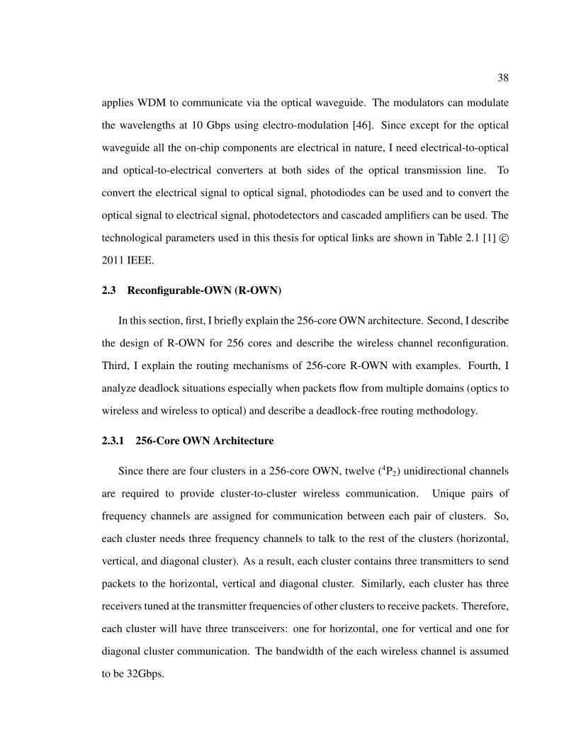
2.3.1 256-Core OWN Architecture
Since there are four clusters in a 256-core OWN, twelve (4P2) unidirectional channels
are required to provide cluster-to-cluster wireless communication. Unique pairs of
frequency channels are assigned for communication between each pair of clusters. So,
each cluster needs three frequency channels to talk to the rest of the clusters (horizontal,
vertical, and diagonal cluster). As a result, each cluster contains three transmitters to send
packets to the horizontal, vertical and diagonal cluster. Similarly, each cluster has three
receivers tuned at the transmitter frequencies of other clusters to receive packets. Therefore,
each cluster will have three transceivers: one for horizontal, one for vertical and one for
diagonal cluster communication. The bandwidth of the each wireless channel is assumed
to be 32Gbps.
39
Figure 2.6: 256-core OWN architecture. Routers with the same color communicate witheach other and Fxy represents a wireless channel to send packets from cluster x to cluster y.For example, Routers H0 and H1 communicate with each other over frequency channel F01and F10 respectively while routers V1 and V3 communicate with each other over frequencychannel F13 and F31 respectively.
Three of the four corner routers of each cluster (Figure 2.1) are chosen for the
on-chip wireless communication. The corner routers are chosen to provide maximum
separation between transceivers operating at different frequencies to minimize inter-
channel interference. The innermost corner routers (marked with red box in Figure 2.6)
of 256-core OWN are not used for the convenience of scaling to 1024-core OWN (Figure
2.3) which has been discussed in the previous section.
40
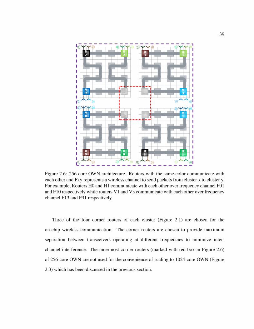
Figure 2.7: Left: Structure of 256-core R-OWN architecture. Right: Structure of a wirelessrouter in R-OWN with transmitters, receivers, counters, and local arbiter [8].
2.3.2 256-Core R-OWN Architecture
OWN 256-core architecture is extended to R-OWN architecture by incorporating
reconfigurability into the network. Each cluster of R-OWN is assigned an adaptive wireless
channel in addition to the fixed wireless channels present in the OWN 256-core network.
So, each wireless router of a cluster contains a transmitter tuned to the adaptive wireless
channel frequency assigned to that cluster and a receiver tuned to the adaptive wireless
channel frequency assigned to other clusters. However, only one of the wireless routers can
operate for a period of time to maintain signal integrity which is determined by an arbiter
(called a local arbiter) located inside the cluster. Therefore, a cluster contains three wireless
routers, three fixed transceiver antennas to communicate with the horizontal, vertical, and
diagonal clusters, three adaptive transceiver antennas, and an arbiter to control the adaptive
transceiver antennas. Since we require 16 channels with a total wireless bandwidth of
512 Gbps, the bandwidth of a wireless channel is 32 Gbps. The architecture of 256-core
R-OWN is shown in Figure 2.7
41
The adaptive wireless channel of each cluster is reconfigured after a reconfiguration
window (set to 100 cycles in our simulation) depending on the number of packets sent to
the other clusters. After every 100 cycles, the local arbiter requests for the wireless link
usages from the wireless routers. Upon receiving the request signal, each wireless router
of a cluster sends their corresponding wireless link utilizations to the local arbiter of this
cluster. The local arbiter determines the destination cluster of the adaptive wireless link for
the next 100 cycles based on the maximum link utilization, resets its counter to zero, sends
a decision signal to each of the wireless router of this cluster, and waits for 100 cycles to
send again a request signal. Upon receiving the decision signal, a wireless router resets
its counter and turns on/off its adaptive antennas. Hence, each wireless router requires
a counter to keep track of the wireless link traversals; each cluster requires an arbiter to
configure adaptive wireless link; and each arbiter requires a counter to count the number of
cycles.
Reconfigurable-Wireless Algorithm
Step 1 Wait for the reconfiguration window, RW
Step 2 Local arbiter, LAi requests the wireless routers (Hi, Vi, Di) for wireless link usage
(WLHi, WLVi, WLDi) where i is the cluster number
Step 3 Hi, Vi, and Di sends WLHi, WLVi, WLDi respectively to LAi
Step 4 LAi finds the maximum of [WLHi, WLVi, WLDi], resets its counter, and sends a
control packet to Hi, Vi, and Di
Step 5 Hi, Vi, and Di respectively resets WLHi, WLVi, WLDi to zero and turn on/off adaptive
antennas
Step 6 Goto Step1
As shown in Figure 2.7, a local arbiter is connected to the wireless routers via metallic
links. In this thesis, I assumed a flit size of 64 bits with four flits in a packet. Hence, a

42
packet takes 8 cycles to transmit through the wireless link. Therefore, each wireless router
requires a 4-bit counter, and each arbiter requires a 7-bit counter. Since the size of the
counters and the width of the metallic links are small, the overhead is insignificant; and
thus, ignored in the performance evaluation (chapter 4).
2.3.3 Routing Mechanism of 256-Core R-OWN
There are four clusters in a 256-core R-OWN where each cluster contains 16 routers
and each router connects 4 cores. A core is represented by a 3-digit coordinate with cluster,
router, and core number as follows: (cs, r, c) where cs is cluster, r is router, and c is core
number. Thus, the total number of cores in R-OWN is cs × r × c, where 0 ≤ cs ≤ 3,
0 ≤ r ≤ 15, and 0 ≤ c ≤ 3. Since cores communicate through routers, I drop the core index
when identifying a router.
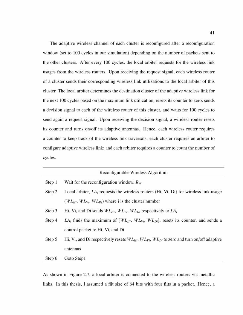
Consider the R-OWN communication shown in Figure 2.8. For example, core (0, 0,
0) and core (0, 7, 2) both want to send a packet to core (1, 7, 3), and router (0, 3) (H0)
possess the adaptive wireless link of cluster 0. In other words, the adaptive wireless link
F0 is connected to cluster 1 at this point of time. Both the cores will need to send a packet
to the router H0 for inter-cluster wireless transmission. By modulating the wavelengths
associated with router H0, one of the cores will send a packet first, and then the next core
will send a packet. Assume both the packets are now sitting at the input buffers of router
H0. Since two wireless links (one fixed, F01 and one adaptive, F0) are now connected to the
wireless router H1 of cluster 1, these two packets will be sent concurrently using frequency
channel F01 and F0. At the same reconfiguration time frame, for example, two cores
of cluster 0 want to send packets to cluster 2 which requires the use of vertical wireless
link (F02). Since only one wireless link is connected to cluster 2 from cluster 0, both
the packets will contend for F02 at router V0 and packets will be transmitted serially. In
contrast, say the adaptive wireless link of cluster 1 (F1) is pointing to cluster 3 as shown
43
Figure 2.8: Communication mechanism of 256-core R-OWN. The large dotted linerepresents fixed wireless link, small dotted line represents adaptive wireless link and thesolid line represents optical link. Routers of the same color talk to each other [8].
in Figure 2.8. Hence, core (1, 13, 2) and core (1, 11, 1) both will be able to send packets
at the same time–using fixed wireless channel, F13 and adaptive wireless channel, F1–to
their destination cluster 3 once the packets reach the wireless router V1. This is possible,
because each cluster has its own adaptive wireless link which is configured based on the
outgoing traffic from this cluster only. Now, consider core (1, 13, 2) send the packet first
to destination core (3, 7, 1) using wireless link F13. Then if core (1, 11, 1) wants to talk to
core (3, 0, 3), router V1 will use the wireless channel F1 instead of F13 as F13 was used
last time. I chose to send packets using the adaptive and fixed wireless links alternatively to
minimize contention. However, when a wireless router does not have access to the adaptive
wireless link, I use the dedicated wireless link to communicate with the other clusters.
44
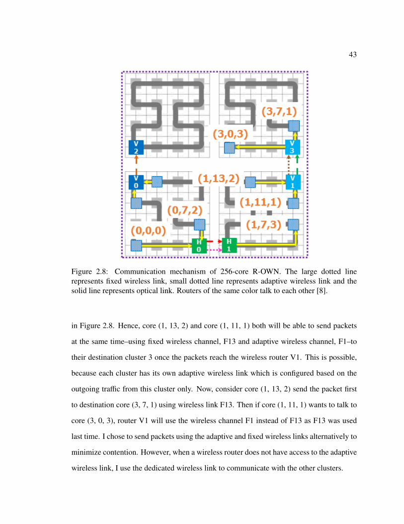
Figure 2.9: (a) Possible deadlock scenario in a 256-core R-OWN for simultaneoustransmission of inter-cluster packets A, B, and C. (b) Proposed network with inclusionof new optical links to avoid deadlocks. A packet is marked with the color of the channelit is using [8].
2.3.4 Deadlock Free Routing
Since R-OWN requires optical to wireless to optical domain transitions, cyclic
dependency exists between the channels which may create deadlock. This is shown in
Figure 2.9 (a) for three packets A, B, and C. Travel paths of packet A, B, and C are D0-
H0-H1-V1, H1-V1-V3-D3, and V3-D3-D0-H0 respectively. Because packet A and C, or
B and A, or C and B use the same optical link, deadlock may occur. There are different
techniques to avoid deadlocks. For R-OWN, I have provided additional channels with
usage restrictions to avoid deadlocks and improve buffer utilization compared to OWN.
I assign new optical links for inter-cluster packets from the source router to the wireless
router. However, on the destination cluster, packets use the optical links that were present
before. As a result, for example, packet A and C take different optical links to travel from

45
router D0 to router H0 which breaks the cyclic dependency. As shown in Figure 2.9 (b),
the proposed network is deadlock-free which ensures all packet delivery. Since an optical
waveguide can contain maximum 64 wavelengths and I can insert these additional optical
links to the existing data waveguide, the tradeoff is increased optical power consumption.
46
3 Off-Chip Interconnection Network
In this chapter, I propose to use wireless technology for both on-chip and off-chip
communications by doing a design space exploration combining wireless and metallic
technology for both on-chip and off-chip communications. Due to the pin bandwidth
limitation, the number of memory controllers used to access the off-chip memory (DRAM)
is not proportionally increasing with the number of cores [47]. In a traditional mesh-based
NoC architecture, the memory controllers are connected at the corner routers only due
to this pin restrictions. Therefore, as core count increases, packets would require more
hops to access off-chip memory which would contribute to an increase in latency and
energy consumption. For example, with private L1 and shared L2 caches, the on-chip
communication delay which comprised of the request packet delay from L1 to L2 and L2
to memory and the response packet delay from memory to L2 and L2 to L1 is significant
[48]. Moreover, the off-chip metallic link connecting the memory controller to the DRAM
cannot be traversed in a single cycle [49]. This would incur additional delay for off-chip
memory accesses.
The problem of longer off-chip memory access latency can be addressed in two
potential ways: (1) by reducing the processing core to the memory controller (request
message) latency and the memory controller to the processing core (response message)
latency, and/or (2) reducing the link traversal latency that connects the memory controller to
the DRAM. Since connecting all the cores directly to the memory controllers using metallic
interconnects is not convenient, positioning the memory controllers carefully on the chip
would dramatically improve the delay scenario [47]. However, this would only partially
solve the problem because the processing cores further away from the memory controller
will still see significant latency. Moreover, on-chip memory controller placement will not
reduce off-chip link traversal latency. Therefore, I propose to use wireless technology
for on-chip as well as off-chip communication to improve both the latency and energy-
47
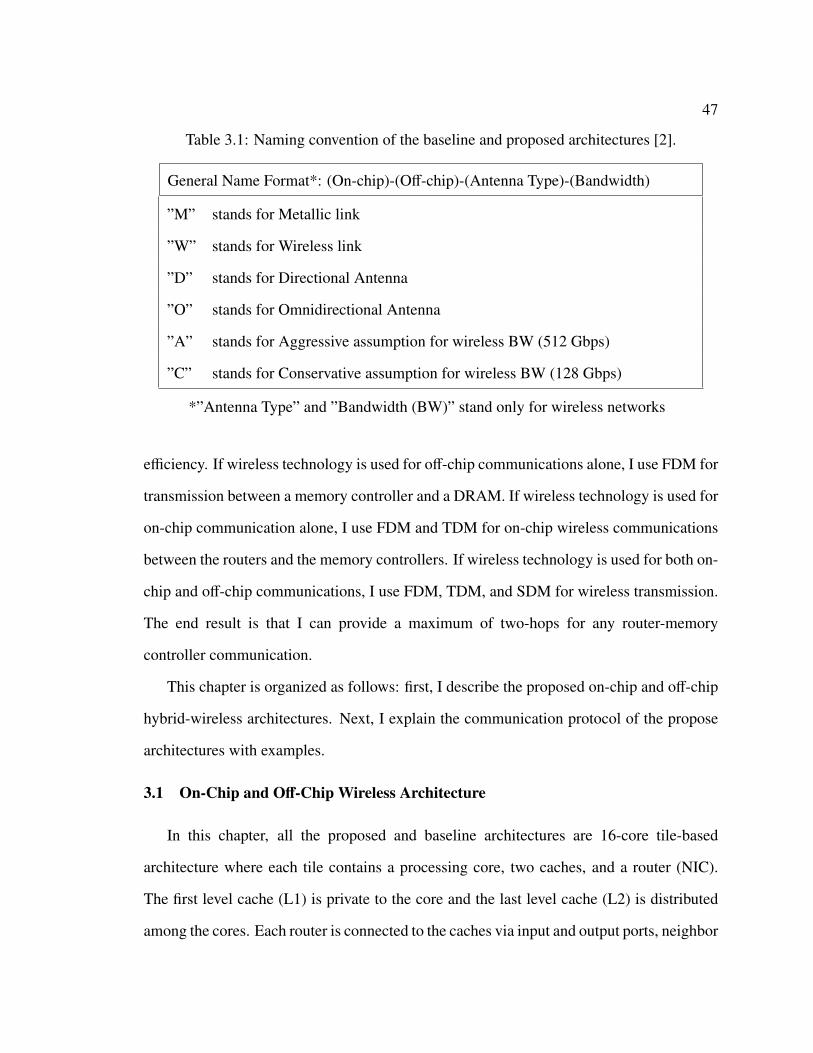
Table 3.1: Naming convention of the baseline and proposed architectures [2].
General Name Format*: (On-chip)-(Off-chip)-(Antenna Type)-(Bandwidth)
”M” stands for Metallic link
”W” stands for Wireless link
”D” stands for Directional Antenna
”O” stands for Omnidirectional Antenna
”A” stands for Aggressive assumption for wireless BW (512 Gbps)
”C” stands for Conservative assumption for wireless BW (128 Gbps)
*”Antenna Type” and ”Bandwidth (BW)” stand only for wireless networks
efficiency. If wireless technology is used for off-chip communications alone, I use FDM for
transmission between a memory controller and a DRAM. If wireless technology is used for
on-chip communication alone, I use FDM and TDM for on-chip wireless communications
between the routers and the memory controllers. If wireless technology is used for both on-
chip and off-chip communications, I use FDM, TDM, and SDM for wireless transmission.
The end result is that I can provide a maximum of two-hops for any router-memory
controller communication.
This chapter is organized as follows: first, I describe the proposed on-chip and off-chip
hybrid-wireless architectures. Next, I explain the communication protocol of the propose
architectures with examples.
3.1 On-Chip and Off-Chip Wireless Architecture
In this chapter, all the proposed and baseline architectures are 16-core tile-based
architecture where each tile contains a processing core, two caches, and a router (NIC).
The first level cache (L1) is private to the core and the last level cache (L2) is distributed
among the cores. Each router is connected to the caches via input and output ports, neighbor
48
Figure 3.1: General structure of baseline and proposed off-chip wireless architectures. (a)Baseline architecture with both on-chip and off-chip metallic interconnects. (b) Metallicinterconnects for on-chip and wireless interconnects for off-chip communication [2].
routers, a processing core, and memory controllers. The memory controllers are considered
as a switch that can arbitrate between multiple memory requests [47]. The naming
convention of the architectures used in this chapter is given in Table 3.1. For example,
consider the architecture M-M-X-X. Both the first “M” (on-chip) and the second “M” (off-
chip) suggest that the network links are metallic. Because the metallic interconnects are not
constrained in terms of bandwidth and cannot be categorized in different types, the last two
parts are written as “X” (don’t care). The name W-M-O-A indicates that the architecture
uses wireless interconnects for on-chip communication and metallic interconnects for off-
chip communication. The last two letters state that the antenna used for on-chip wireless
network is omnidirectional in nature and the overall bandwidth is 512 Gbps (shown in
3.1). Similarly, W-W-D-C enunciates that both the on-chip and off-chip networks employ
wireless technology for communication using directional antenna having overall bandwidth
of 128 Gbps.
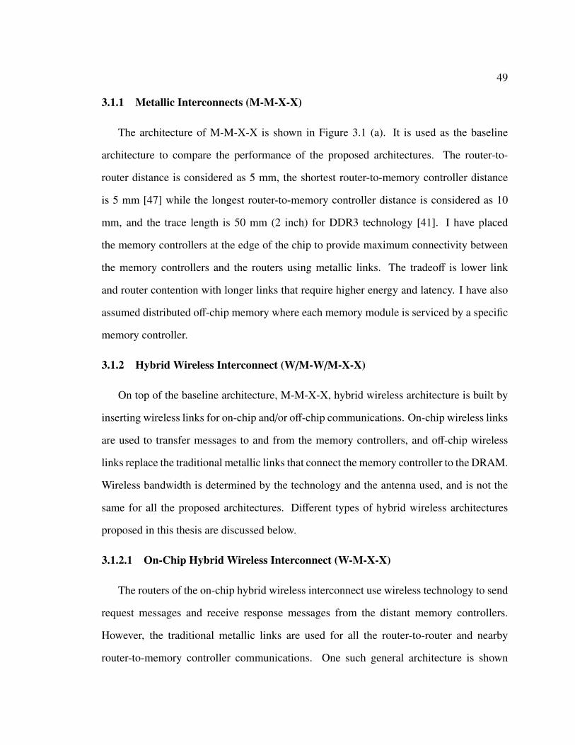
49
3.1.1 Metallic Interconnects (M-M-X-X)
The architecture of M-M-X-X is shown in Figure 3.1 (a). It is used as the baseline
architecture to compare the performance of the proposed architectures. The router-to-
router distance is considered as 5 mm, the shortest router-to-memory controller distance
is 5 mm [47] while the longest router-to-memory controller distance is considered as 10
mm, and the trace length is 50 mm (2 inch) for DDR3 technology [41]. I have placed
the memory controllers at the edge of the chip to provide maximum connectivity between
the memory controllers and the routers using metallic links. The tradeoff is lower link
and router contention with longer links that require higher energy and latency. I have also
assumed distributed off-chip memory where each memory module is serviced by a specific
memory controller.
3.1.2 Hybrid Wireless Interconnect (W/M-W/M-X-X)
On top of the baseline architecture, M-M-X-X, hybrid wireless architecture is built by
inserting wireless links for on-chip and/or off-chip communications. On-chip wireless links
are used to transfer messages to and from the memory controllers, and off-chip wireless
links replace the traditional metallic links that connect the memory controller to the DRAM.
Wireless bandwidth is determined by the technology and the antenna used, and is not the
same for all the proposed architectures. Different types of hybrid wireless architectures
proposed in this thesis are discussed below.
3.1.2.1 On-Chip Hybrid Wireless Interconnect (W-M-X-X)
The routers of the on-chip hybrid wireless interconnect use wireless technology to send
request messages and receive response messages from the distant memory controllers.
However, the traditional metallic links are used for all the router-to-router and nearby
router-to-memory controller communications. One such general architecture is shown
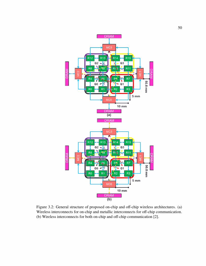
50
Figure 3.2: General structure of proposed on-chip and off-chip wireless architectures. (a)Wireless interconnects for on-chip and metallic interconnects for off-chip communication.(b) Wireless interconnects for both on-chip and off-chip communication [2].
51
in Figure 3.2 (a). The on-chip routers are divided into four groups where each group
contains four routers. Each group is assigned a unique frequency channel to transmit
messages to the distant memory controllers while metallic links are used for nearby
memory controllers. Similarly, each memory controller is assigned a unique frequency
channel to transmit data to the distant router-groups while it uses metallic links for nearby
router-groups. I have considered two types of antennas- omnidirectional and directional
and two wireless bandwidth assumptions- conservative and aggressive. This provides four
different architecture designs. Nevertheless, I have not considered W-M-O-C because
wireless bandwidth of 512 Gbps (aggressive assumption) for omnidirectional type antenna
is well established [1, 3]. Other architectures considered are described below:
• W-M-O-A: As shown in Figure 3.2 (a), the routers of a group share the frequency
channel assigned to the group for sending messages to the memory controllers. For
example, group G0 is assigned a frequency channel to send a message to the memory
controllers MC1 and MC3. The routers (R0, R1, R4, and R5) of G0 share the
frequency channel using a token to maintain signal integrity. Since omnidirectional
antenna is used for wireless communication, both MC1 and MC3 can receive the data
at the same time and then discard if that message is not destined for it. Similarly,
memory controller MC1 uses a frequency channel to send data to the groups G0
and G2 (R8, R9, R12, and R13). Therefore, each router of a group contains one
transmitter to send data to the distant memory controllers and two receivers to receive
data from the distant memory controllers. Each memory controller also contains a
transmitter to send data to the distant router groups and two receivers to receive data
from the distant router groups.
• W-M-D-A: The basic architecture of W-M-D-A is similar to the W-M-O-A
architecture. However, two antennas are required to send data because the antenna
used for wireless communication is a directional type. For example, router R0 of
52
group G0 contains two transmitters: one for sending data to memory controller MC1
and the other to MC3. When router R0 has the token to transmit, it uses one of the two
transmitters depending on the destination memory controller. Similarly, the memory
controller, for example MC1, uses two transmitters to send data to the routers of
groups G0 and G2. Both these transmitters of a router or a memory controller are
tuned at the same frequency. Although the number of transmitters required in W-M-
D-A is double compared to W-M-O-A, in both the number of receivers is the same.
• W-M-D-C: The structure of W-M-D-C is the same as W-M-D-A architecture. The
only difference is the wireless bandwidth used. The wireless link bandwidth of W-
M-D-C is one fourth of the wireless link bandwidth of W-M-D-A. Hence, the latency
for W-M-D-C would be higher than for W-M-D-A.
3.1.2.2 Off-Chip Hybrid Wireless Interconnect (M-W-X-X)
M-W-X-X has the same on-chip architecture as M-M-X-X architecture. However, M-
W-X-X employs wireless links to communicate with the off-chip memory as shown in
Figure 3.1 (b). For this purpose, each memory controller contains a transmitter and a
receiver that is tuned at the frequency of the corresponding DRAMs transmitter. Hence, the
DRAM needs to facilitate a transmitter and to have a receiver that is tuned at the frequency
of the corresponding memory controllers transmitter.
3.1.2.3 On-Chip and Off-Chip Hybrid Wireless Interconnect (W-W-X-X)
This architecture combines the on-chip architecture W-M-X-X and off-chip architecture
M-W-X-X. Since both the on-chip and off-chip networks use wireless technology, I use
SDM technique to overcome the frequency bandwidth limitation. One such architecture is
shown in Figure 3.2 (b). A summary of all the architectures described previously are shown
in Table 3.2.
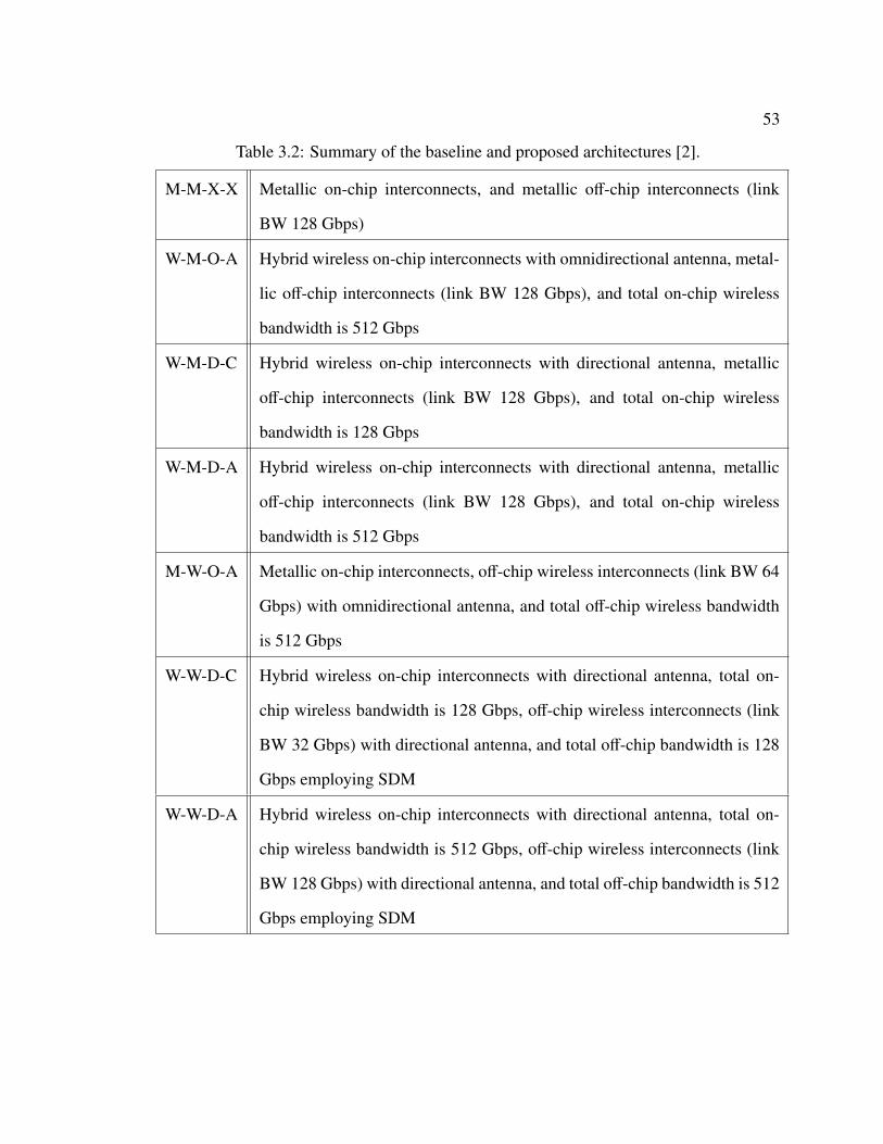
53
Table 3.2: Summary of the baseline and proposed architectures [2].
M-M-X-X Metallic on-chip interconnects, and metallic off-chip interconnects (link
BW 128 Gbps)
W-M-O-A Hybrid wireless on-chip interconnects with omnidirectional antenna, metal-
lic off-chip interconnects (link BW 128 Gbps), and total on-chip wireless
bandwidth is 512 Gbps
W-M-D-C Hybrid wireless on-chip interconnects with directional antenna, metallic
off-chip interconnects (link BW 128 Gbps), and total on-chip wireless
bandwidth is 128 Gbps
W-M-D-A Hybrid wireless on-chip interconnects with directional antenna, metallic
off-chip interconnects (link BW 128 Gbps), and total on-chip wireless
bandwidth is 512 Gbps
M-W-O-A Metallic on-chip interconnects, off-chip wireless interconnects (link BW 64
Gbps) with omnidirectional antenna, and total off-chip wireless bandwidth
is 512 Gbps
W-W-D-C Hybrid wireless on-chip interconnects with directional antenna, total on-
chip wireless bandwidth is 128 Gbps, off-chip wireless interconnects (link
BW 32 Gbps) with directional antenna, and total off-chip bandwidth is 128
Gbps employing SDM
W-W-D-A Hybrid wireless on-chip interconnects with directional antenna, total on-
chip wireless bandwidth is 512 Gbps, off-chip wireless interconnects (link
BW 128 Gbps) with directional antenna, and total off-chip bandwidth is 512
Gbps employing SDM
54
3.2 Communication Protocol: Metallic and Hybrid Wireless Interconnect
In this thesis, I assume that each processing core requests necessary data from its private
L1 cache. If there is an L1 miss, then a request message is sent through the router to
the L2 cache containing the necessary data. On an L2 miss, a request message is sent
to the memory controller that is servicing the memory module containing the latest data.
After performing the read operation, a DRAM sends the data to the memory controller
that requested the data. Since memories are inclusive, a response message carrying the
data is sent to the requesting routers L2 cache, and then this router sends the data to
the source routers L1 cache. This is the basic communication protocol followed in this
chapter. Following are the architecture specific communication mechanisms. Since an off-
chip wireless or metallic link transmission is identical in terms of communication protocol,
I only focus on on-chip communication in this section.
3.2.1 On-Chip Metallic and Off-Chip Metallic or Wireless Interconnects
Figure 3.3 (a) shows the communication mechanism for an on-chip metallic link based
architecture where the off-chip messages are sent via wireless or metallic links. For
example, if there is a miss at the L1 cache connected to router R0 and this address space is
serviced by the L2 cache connected to router R9, then the L1 cache needs to send a request
message through R0 to the L2 cache via R9. The request message follows the DOR protocol
to reach R9 from R0. If the L2 cache has the updated data, a response message is sent to
R0. However, if there is an L2 miss, then router R9 sends a new request message to the
memory controller servicing that address space. Consider that the memory controller MC3
is servicing the address space of the L2 cache connected to router R9. Hence, R9 sends
a message requesting updated data to MC3, and the message utilizes the DOR protocol
to reach MC3. MC3 sends the necessary signal to the memory module to perform the
read operation either using the metallic link or the wireless link. Upon receiving the data
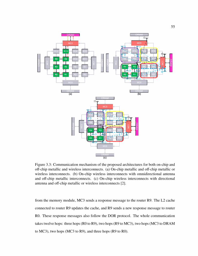
55
Figure 3.3: Communication mechanism of the proposed architectures for both on-chip andoff-chip metallic and wireless interconnects. (a) On-chip metallic and off-chip metallic orwireless interconnects. (b) On-chip wireless interconnects with omnidirectional antennaand off-chip metallic interconnects. (c) On-chip wireless interconnects with directionalantenna and off-chip metallic or wireless interconnects [2].
from the memory module, MC3 sends a response message to the router R9. The L2 cache
connected to router R9 updates the cache, and R9 sends a new response message to router
R0. These response messages also follow the DOR protocol. The whole communication
takes twelve hops: three hops (R0 to R9), two hops (R9 to MC3), two hops (MC3 to DRAM
to MC3), two hops (MC3 to R9), and three hops (R9 to R0).
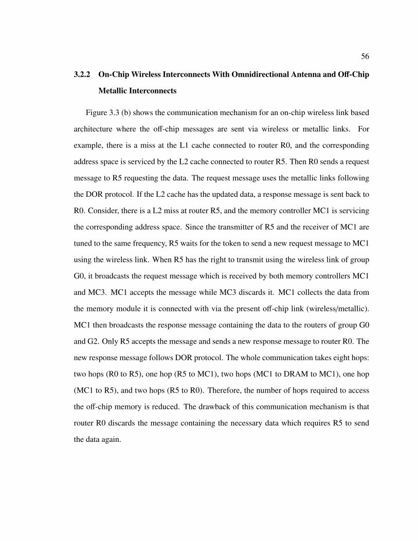
56
3.2.2 On-Chip Wireless Interconnects With Omnidirectional Antenna and Off-Chip
Metallic Interconnects
Figure 3.3 (b) shows the communication mechanism for an on-chip wireless link based
architecture where the off-chip messages are sent via wireless or metallic links. For
example, there is a miss at the L1 cache connected to router R0, and the corresponding
address space is serviced by the L2 cache connected to router R5. Then R0 sends a request
message to R5 requesting the data. The request message uses the metallic links following
the DOR protocol. If the L2 cache has the updated data, a response message is sent back to
R0. Consider, there is a L2 miss at router R5, and the memory controller MC1 is servicing
the corresponding address space. Since the transmitter of R5 and the receiver of MC1 are
tuned to the same frequency, R5 waits for the token to send a new request message to MC1
using the wireless link. When R5 has the right to transmit using the wireless link of group
G0, it broadcasts the request message which is received by both memory controllers MC1
and MC3. MC1 accepts the message while MC3 discards it. MC1 collects the data from
the memory module it is connected with via the present off-chip link (wireless/metallic).
MC1 then broadcasts the response message containing the data to the routers of group G0
and G2. Only R5 accepts the message and sends a new response message to router R0. The
new response message follows DOR protocol. The whole communication takes eight hops:
two hops (R0 to R5), one hop (R5 to MC1), two hops (MC1 to DRAM to MC1), one hop
(MC1 to R5), and two hops (R5 to R0). Therefore, the number of hops required to access
the off-chip memory is reduced. The drawback of this communication mechanism is that
router R0 discards the message containing the necessary data which requires R5 to send
the data again.
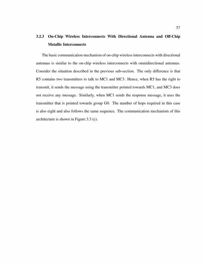
57
3.2.3 On-Chip Wireless Interconnects With Directional Antenna and Off-Chip
Metallic Interconnects
The basic communication mechanism of on-chip wireless interconnects with directional
antennas is similar to the on-chip wireless interconnects with omnidirectional antennas.
Consider the situation described in the previous sub-section. The only difference is that
R5 contains two transmitters to talk to MC1 and MC3. Hence, when R5 has the right to
transmit, it sends the message using the transmitter pointed towards MC1, and MC3 does
not receive any message. Similarly, when MC1 sends the response message, it uses the
transmitter that is pointed towards group G0. The number of hops required in this case
is also eight and also follows the same sequence. The communication mechanism of this
architecture is shown in Figure 3.3 (c).
58
4 Evaluation of the Proposed Architectures
In this chapter, I analyze the performance of the proposed architectures- OWN, R-
OWN, and On-Chip and Off-Chip Wireless Network by comparing against the state-of-the-
art wired, wireless, or photonic architectures. I restrict my focus to only the area, energy
per bit, latency, and saturation throughput comparison because these are the most critical
parameters of an interconnection network.
The area of an architecture is calculated as a sum of the link (wired, wireless, and
optical) area, router area, wireless transceiver area (wireless networks), and waveguide
area (photonic networks) [1]. I have used Dsent v. 0.91 [49] to calculate the area and
the energy of the wired links and routers for a bulk 45nm LVT technology [1]. For a
wireless link, I have assumed the transmitter area as 0.42 mm2 and the receiver area as
0.20 mm2 [38]. Photonic link area consists of the power, data, and arbitration waveguide
area. To calculate the wired/wireless link energy consumption, I have multiplied the
number of wired/wireless link traversals, collected from the cycle accurate simulation, to
the corresponding wired/wireless link energy [1]. For all the architectures, wireless link
energy-efficiency is assumed to be 1 pJ/bit for on-chip communication and considering a
linear increase, is estimated for off-chip communication [37]. I have assumed a fixed 1
pJ per bit energy consumption for all the on-chip wireless architectures [1]. To calculate
the optical link energy consumption, I have considered the worst case scenario and used
the values of the parameters shown in Table 2.1 [1]. When calculating the router energy
consumption, because Dsent gives the total buffer and crossbar power, I have divided the
buffer energy with the number of buffers and divided the crossbar energy with the radix of
the router [1]. In order for a fair comparison between different topologies, I have kept the
bisection bandwidth and the clock period of the network the same for all the architectures
during simulation. For fairness, I have kept the same number of VC and buffer for all the
architectures [1].
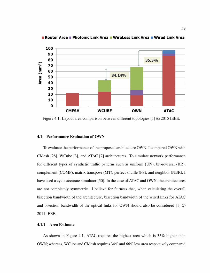
59
Figure 4.1: Layout area comparison between different topologies [1]© 2015 IEEE.
4.1 Performance Evaluation of OWN
To evaluate the performance of the proposed architecture OWN, I compared OWN with
CMesh [28], WCube [3], and ATAC [7] architectures. To simulate network performance
for different types of synthetic traffic patterns such as uniform (UN), bit-reversal (BR),
complement (COMP), matrix transpose (MT), perfect shuffle (PS), and neighbor (NBR), I
have used a cycle accurate simulator [50]. In the case of ATAC and OWN, the architectures
are not completely symmetric. I believe for fairness that, when calculating the overall
bisection bandwidth of the architecture, bisection bandwidth of the wired links for ATAC
and bisection bandwidth of the optical links for OWN should also be considered [1] ©
2011 IEEE.
4.1.1 Area Estimate
As shown in Figure 4.1, ATAC requires the highest area which is 35% higher than
OWN; whereas, WCube and CMesh requires 34% and 66% less area respectively compared
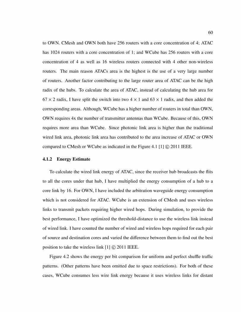
60
to OWN. CMesh and OWN both have 256 routers with a core concentration of 4; ATAC
has 1024 routers with a core concentration of 1; and WCube has 256 routers with a core
concentration of 4 as well as 16 wireless routers connected with 4 other non-wireless
routers. The main reason ATACs area is the highest is the use of a very large number
of routers. Another factor contributing to the large router area of ATAC can be the high
radix of the hubs. To calculate the area of ATAC, instead of calculating the hub area for
67 × 2 radix, I have split the switch into two 4 × 1 and 63 × 1 radix, and then added the
corresponding areas. Although, WCube has a higher number of routers in total than OWN,
OWN requires 4x the number of transmitter antennas than WCube. Because of this, OWN
requires more area than WCube. Since photonic link area is higher than the traditional
wired link area, photonic link area has contributed to the area increase of ATAC or OWN
compared to CMesh or WCube as indicated in the Figure 4.1 [1]© 2011 IEEE.
4.1.2 Energy Estimate
To calculate the wired link energy of ATAC, since the receiver hub broadcasts the flits
to all the cores under that hub, I have multiplied the energy consumption of a hub to a
core link by 16. For OWN, I have included the arbitration waveguide energy consumption
which is not considered for ATAC. WCube is an extension of CMesh and uses wireless
links to transmit packets requiring higher wired hops. During simulation, to provide the
best performance, I have optimized the threshold-distance to use the wireless link instead
of wired link. I have counted the number of wired and wireless hops required for each pair
of source and destination cores and varied the difference between them to find out the best
position to take the wireless link [1]© 2011 IEEE.
Figure 4.2 shows the energy per bit comparison for uniform and perfect shuffle traffic
patterns. (Other patterns have been omitted due to space restrictions). For both of these
cases, WCube consumes less wire link energy because it uses wireless links for distant
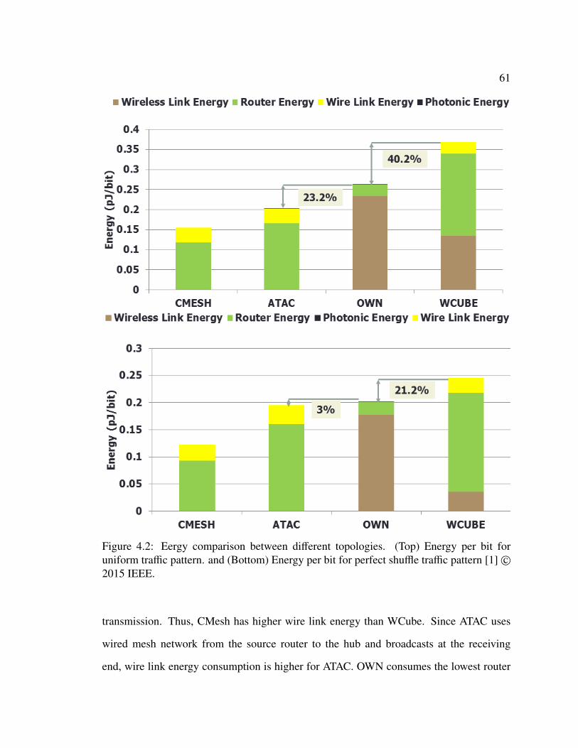
61
Figure 4.2: Eergy comparison between different topologies. (Top) Energy per bit foruniform traffic pattern. and (Bottom) Energy per bit for perfect shuffle traffic pattern [1]©2015 IEEE.
transmission. Thus, CMesh has higher wire link energy than WCube. Since ATAC uses
wired mesh network from the source router to the hub and broadcasts at the receiving
end, wire link energy consumption is higher for ATAC. OWN consumes the lowest router
62
energy. This is due to the lower radix of the split router and also that OWN requires
only three hops. Furthermore, because increasing the router radix decreases the energy
consumption compared to multiple router traversals [51], the energy per bit requirement
of OWN is reduced. WCube not only has a higher number of routers but also the radix
of some routers is higher compared to CMesh. ATAC has the highest number of routers
among the four, but ATAC still consumes less router energy than WCube. This is because
WCube shares a single router with 64-cores whereas ATAC shares the router with only
16-cores. WCube has a lower wireless link energy requirement than OWN since WCube
employs wireless links only for distant packets. In contrast, OWN uses wireless links for all
the inter-cluster transmission whether the clusters are neighbors or not. Figure 4.2 shows
that for uniform traffic, OWN consumes 23% higher energy/bit than ATAC and 40% less
energy/bit than WCube; and for perfect shuffle traffic, OWN consumes only 3% higher
energy/bit than ATAC and 21% lower energy/bit than WCube. The energy overhead of
OWN is mostly caused by wireless link energy as can be seen in Figure 4.2. The reduction
of energy per bit of WCube from uniform to perfect shuffle traffic is due to the lower use
of wireless links which is also true for OWN. However, the wireless link energy per bit
requirement is technology dependent. As advances in technology continue, in terms of
energy consumption, OWN will greatly benefit due to the reduction of wireless link energy
per bit compared to the other architectures [1]© 2011 IEEE.
4.1.3 Saturation Throughput and Latency Comparison
In this sub-section, I briefly discuss the latency and saturation throughput of OWN
compared to CMesh, WCube, and ATAC. To imitate ATAC as closely as possible, I have
subtracted the buffer and crossbar delay for the flits travelling from the destination hub to
the cores to represent the broadcast scheme. Figure 4.3 shows the latency for the traffic
types UN, BR, MT, and NBR as a measure of the number of cycles in response to a varied
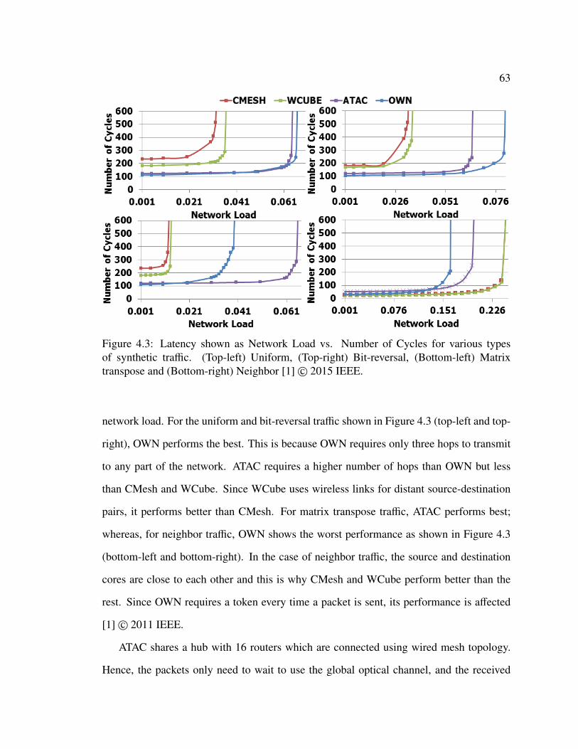
63
Figure 4.3: Latency shown as Network Load vs. Number of Cycles for various typesof synthetic traffic. (Top-left) Uniform, (Top-right) Bit-reversal, (Bottom-left) Matrixtranspose and (Bottom-right) Neighbor [1]© 2015 IEEE.
network load. For the uniform and bit-reversal traffic shown in Figure 4.3 (top-left and top-
right), OWN performs the best. This is because OWN requires only three hops to transmit
to any part of the network. ATAC requires a higher number of hops than OWN but less
than CMesh and WCube. Since WCube uses wireless links for distant source-destination
pairs, it performs better than CMesh. For matrix transpose traffic, ATAC performs best;
whereas, for neighbor traffic, OWN shows the worst performance as shown in Figure 4.3
(bottom-left and bottom-right). In the case of neighbor traffic, the source and destination
cores are close to each other and this is why CMesh and WCube perform better than the
rest. Since OWN requires a token every time a packet is sent, its performance is affected
[1]© 2011 IEEE.
ATAC shares a hub with 16 routers which are connected using wired mesh topology.
Hence, the packets only need to wait to use the global optical channel, and the received
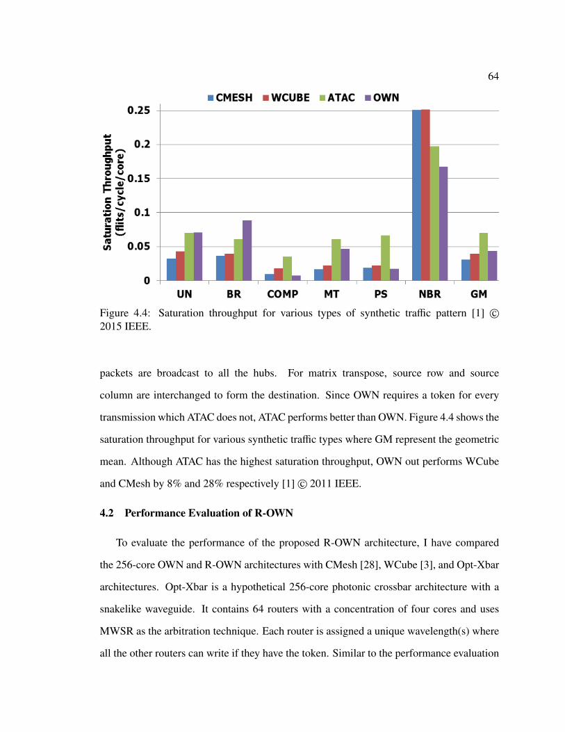
64
Figure 4.4: Saturation throughput for various types of synthetic traffic pattern [1] ©2015 IEEE.
packets are broadcast to all the hubs. For matrix transpose, source row and source
column are interchanged to form the destination. Since OWN requires a token for every
transmission which ATAC does not, ATAC performs better than OWN. Figure 4.4 shows the
saturation throughput for various synthetic traffic types where GM represent the geometric
mean. Although ATAC has the highest saturation throughput, OWN out performs WCube
and CMesh by 8% and 28% respectively [1]© 2011 IEEE.
4.2 Performance Evaluation of R-OWN
To evaluate the performance of the proposed R-OWN architecture, I have compared
the 256-core OWN and R-OWN architectures with CMesh [28], WCube [3], and Opt-Xbar
architectures. Opt-Xbar is a hypothetical 256-core photonic crossbar architecture with a
snakelike waveguide. It contains 64 routers with a concentration of four cores and uses
MWSR as the arbitration technique. Each router is assigned a unique wavelength(s) where
all the other routers can write if they have the token. Similar to the performance evaluation
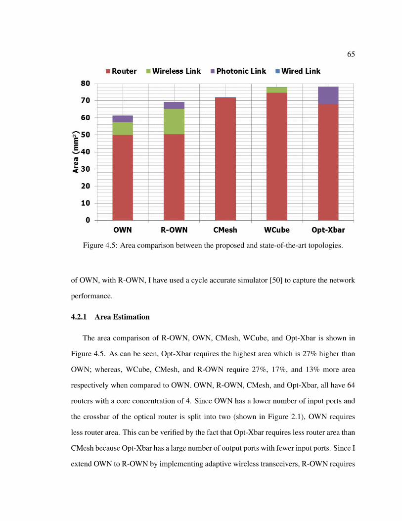
65
Figure 4.5: Area comparison between the proposed and state-of-the-art topologies.
of OWN, with R-OWN, I have used a cycle accurate simulator [50] to capture the network
performance.
4.2.1 Area Estimation
The area comparison of R-OWN, OWN, CMesh, WCube, and Opt-Xbar is shown in
Figure 4.5. As can be seen, Opt-Xbar requires the highest area which is 27% higher than
OWN; whereas, WCube, CMesh, and R-OWN require 27%, 17%, and 13% more area
respectively when compared to OWN. OWN, R-OWN, CMesh, and Opt-Xbar, all have 64
routers with a core concentration of 4. Since OWN has a lower number of input ports and
the crossbar of the optical router is split into two (shown in Figure 2.1), OWN requires
less router area. This can be verified by the fact that Opt-Xbar requires less router area than
CMesh because Opt-Xbar has a large number of output ports with fewer input ports. Since I
extend OWN to R-OWN by implementing adaptive wireless transceivers, R-OWN requires
66
a higher number of wireless transceivers than OWN. As a result, R-OWN requires a higher
wireless link area compared to OWN. R-OWN also requires a slightly higher router area
than OWN due to the increase in the radix of the wireless router (the optical router remains
the same). In this analysis, I have ignored the counter and local arbiter area as they are very
small. Since OWN and thus R-OWN contain several smaller crossbars, OWN and R-OWN
require less photonic link area than Opt-Xbar due to the fact that Opt-Xbar contains one
large crossbar.
4.2.2 Energy Estimate
Figure 4.6 shows the energy per bit comparison for UN, BR, MT, and PS traffic patterns
with the geometric mean. WCube has lesser wireless channels than OWN and R-OWN.
Hence, the number of wireless link traversals and, thus, wireless link energy consumption
for WCube is less compared to OWN and R-OWN. Because R-OWN uses more wireless
channels, it consumes more wireless link energy than OWN. The difference is visible
for MT and PS traffic as for these two traffic patterns, adaptive wireless links are well
utilized which is also reflected in their saturation throughput (Figure 4.7). Since photonic
link energy consumption is much lower than the other technologies, it does not affect the
overall energy consumption significantly. Nevertheless, OWN and R-OWN both consume
an order of magnitude lower energy than Opt-Xbar due to a smaller crossbar size. Opt-
Xbar consumes the lowest router energy because it has a lower number of input and a
higher number of output ports. The first factor contributes to the lower buffer energy while
the second factor contributes to the lower crossbar energy per flit. OWN and R-OWN
both consume lower router energy than CMesh and WCube. This is due to the lower
hop requirement, a lower number of input ports with a higher number of output ports,
and splitting of the crossbar. However, R-OWN requires higher router energy compared
to OWN due to the increase of wireless router radix. Compared to OWN and R-OWN,
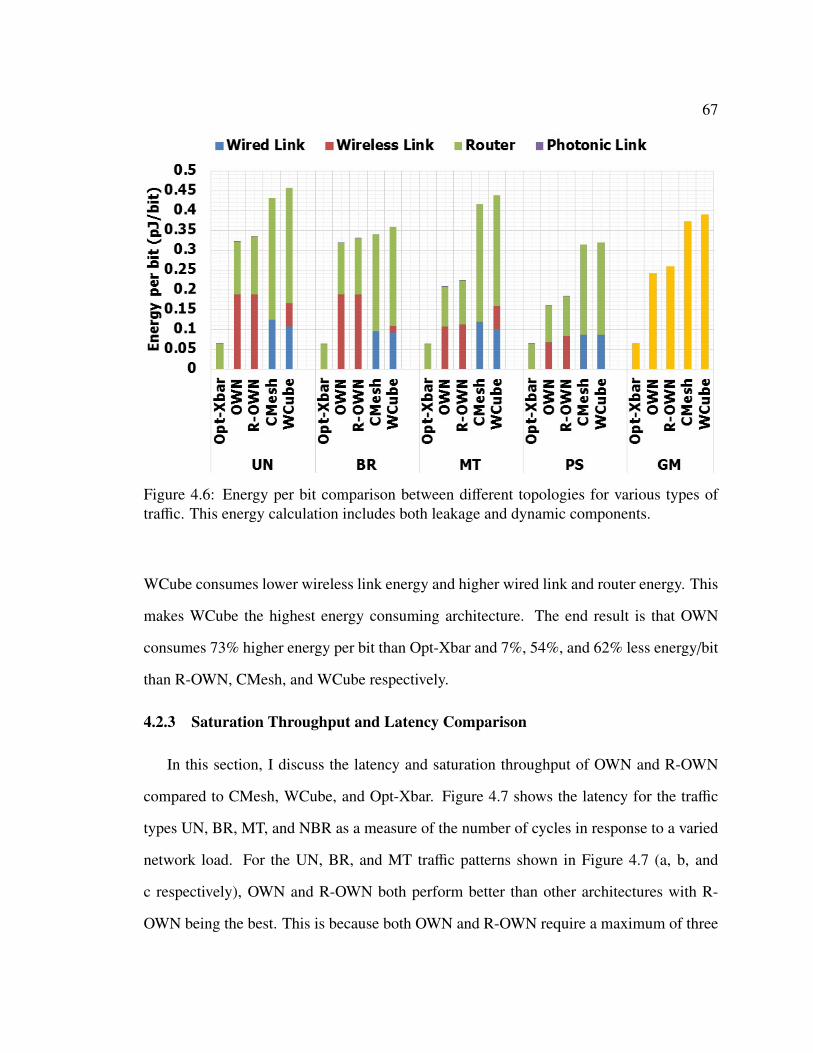
67
Figure 4.6: Energy per bit comparison between different topologies for various types oftraffic. This energy calculation includes both leakage and dynamic components.
WCube consumes lower wireless link energy and higher wired link and router energy. This
makes WCube the highest energy consuming architecture. The end result is that OWN
consumes 73% higher energy per bit than Opt-Xbar and 7%, 54%, and 62% less energy/bit
than R-OWN, CMesh, and WCube respectively.
4.2.3 Saturation Throughput and Latency Comparison
In this section, I discuss the latency and saturation throughput of OWN and R-OWN
compared to CMesh, WCube, and Opt-Xbar. Figure 4.7 shows the latency for the traffic
types UN, BR, MT, and NBR as a measure of the number of cycles in response to a varied
network load. For the UN, BR, and MT traffic patterns shown in Figure 4.7 (a, b, and
c respectively), OWN and R-OWN both perform better than other architectures with R-
OWN being the best. This is because both OWN and R-OWN require a maximum of three
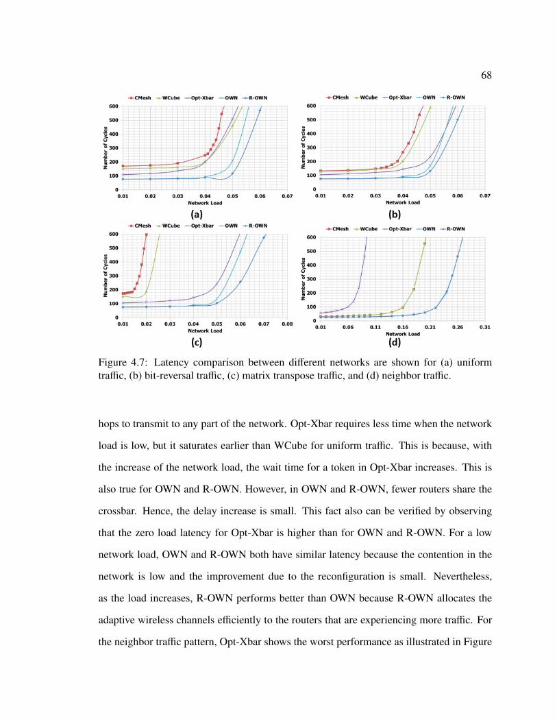
68
Figure 4.7: Latency comparison between different networks are shown for (a) uniformtraffic, (b) bit-reversal traffic, (c) matrix transpose traffic, and (d) neighbor traffic.
hops to transmit to any part of the network. Opt-Xbar requires less time when the network
load is low, but it saturates earlier than WCube for uniform traffic. This is because, with
the increase of the network load, the wait time for a token in Opt-Xbar increases. This is
also true for OWN and R-OWN. However, in OWN and R-OWN, fewer routers share the
crossbar. Hence, the delay increase is small. This fact also can be verified by observing
that the zero load latency for Opt-Xbar is higher than for OWN and R-OWN. For a low
network load, OWN and R-OWN both have similar latency because the contention in the
network is low and the improvement due to the reconfiguration is small. Nevertheless,
as the load increases, R-OWN performs better than OWN because R-OWN allocates the
adaptive wireless channels efficiently to the routers that are experiencing more traffic. For
the neighbor traffic pattern, Opt-Xbar shows the worst performance as illustrated in Figure
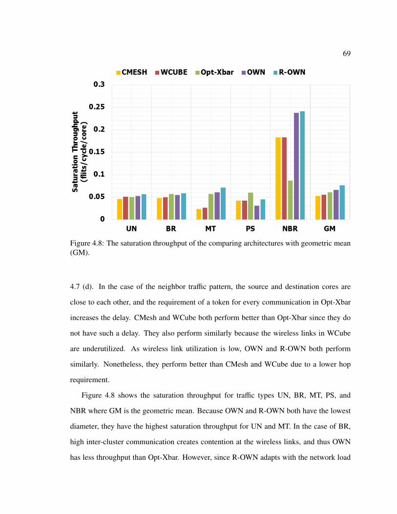
69
Figure 4.8: The saturation throughput of the comparing architectures with geometric mean(GM).
4.7 (d). In the case of the neighbor traffic pattern, the source and destination cores are
close to each other, and the requirement of a token for every communication in Opt-Xbar
increases the delay. CMesh and WCube both perform better than Opt-Xbar since they do
not have such a delay. They also perform similarly because the wireless links in WCube
are underutilized. As wireless link utilization is low, OWN and R-OWN both perform
similarly. Nonetheless, they perform better than CMesh and WCube due to a lower hop
requirement.
Figure 4.8 shows the saturation throughput for traffic types UN, BR, MT, PS, and
NBR where GM is the geometric mean. Because OWN and R-OWN both have the lowest
diameter, they have the highest saturation throughput for UN and MT. In the case of BR,
high inter-cluster communication creates contention at the wireless links, and thus OWN
has less throughput than Opt-Xbar. However, since R-OWN adapts with the network load
70
pattern, R-OWN has the highest throughput. For PS, the utilization of wireless links is
diverse. This causes the saturation throughput of OWN to fall since certain wireless links
are over utilized while the others are underutilized. Hence, for PS, the improvement of R-
OWN with respect to OWN is the highest. As a result, R-OWN has 15% higher saturation
throughput than OWN and OWN has 8%, 16%, and 21% higher saturation throughput than
Opt-Xbar, WCube, and CMesh respectively.
4.3 Performance Evaluation of On-Chip and Off-Chip Wireless Network
The proposed on-chip and off-chip wireless architectures are compared against the
baseline architecture (Table 3.2) to evaluate the performance. I have used a cycle
accurate simulator Multi2Sim [52] to simulate the network performance of the proposed
architectures for PARSEC 2.1 benchmark [53]. The simulation parameters used are shown
in Table 4.1.
4.3.1 Execution Time Estimate
Figure 4.9 shows the execution times of blackscholes benchmark for all the architec-
tures. It can be seen that the proposed architectures, except M-W-O-A and W-W-D-C,
require lower execution times than the baseline architecture M-M-X -X. This is due to the
fact that, for off-chip memory accesses, the proposed architectures require a lower num-
ber of hops than the baseline architecture. Therefore, the hybrid-wireless architectures
that have the highest bandwidth perform the best. Because the off-chip link bandwidth of
W-W-D-C is orders of magnitude lower than the baseline, the improvement achieved by
the hop-count reduction is nullified, and W-W-D-C performs the worst. In the case of M-
W-O-A, there is no reduction in the hop-count for off-chip memory accesses. Moreover,
the off-chip wireless link bandwidth in M-W-O-A is half of the metallic link bandwidth
in M-M-X-X but is higher than the off-chip wireless link bandwidth in W-W-D-C. Hence,
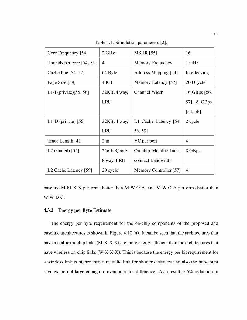
71
Table 4.1: Simulation parameters [2].
Core Frequency [54] 2 GHz MSHR [55] 16
Threads per core [54, 55] 4 Memory Frequency 1 GHz
Cache line [54–57] 64 Byte Address Mapping [54] Interleaving
Page Size [58] 4 KB Memory Latency [52] 200 Cycle
L1-I (private)[55, 56] 32KB, 4 way,
LRU
Channel Width 16 GBps [56,
57], 8 GBps
[54, 56]
L1-D (private) [56] 32KB, 4 way,
LRU
L1 Cache Latency [54,
56, 59]
2 cycle
Trace Length [41] 2 in VC per port 4
L2 (shared) [55] 256 KB/core,
8 way, LRU
On-chip Metallic Inter-
connect Bandwidth
8 GBps
L2 Cache Latency [59] 20 cycle Memory Controller [57] 4
baseline M-M-X-X performs better than M-W-O-A, and M-W-O-A performs better than
W-W-D-C.
4.3.2 Energy per Byte Estimate
The energy per byte requirement for the on-chip components of the proposed and
baseline architectures is shown in Figure 4.10 (a). It can be seen that the architectures that
have metallic on-chip links (M-X-X-X) are more energy efficient than the architectures that
have wireless on-chip links (W-X-X-X). This is because the energy per bit requirement for
a wireless link is higher than a metallic link for shorter distances and also the hop-count
savings are not large enough to overcome this difference. As a result, 5.6% reduction in
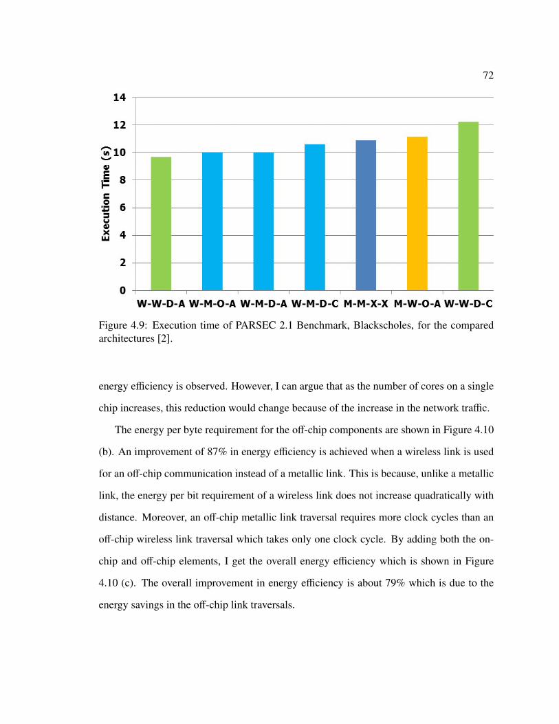
72
Figure 4.9: Execution time of PARSEC 2.1 Benchmark, Blackscholes, for the comparedarchitectures [2].
energy efficiency is observed. However, I can argue that as the number of cores on a single
chip increases, this reduction would change because of the increase in the network traffic.
The energy per byte requirement for the off-chip components are shown in Figure 4.10
(b). An improvement of 87% in energy efficiency is achieved when a wireless link is used
for an off-chip communication instead of a metallic link. This is because, unlike a metallic
link, the energy per bit requirement of a wireless link does not increase quadratically with
distance. Moreover, an off-chip metallic link traversal requires more clock cycles than an
off-chip wireless link traversal which takes only one clock cycle. By adding both the on-
chip and off-chip elements, I get the overall energy efficiency which is shown in Figure
4.10 (c). The overall improvement in energy efficiency is about 79% which is due to the
energy savings in the off-chip link traversals.
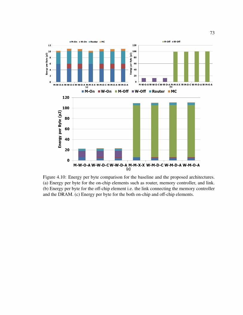
73
Figure 4.10: Energy per byte comparison for the baseline and the proposed architectures.(a) Energy per byte for the on-chip elements such as router, memory controller, and link.(b) Energy per byte for the off-chip element i.e. the link connecting the memory controllerand the DRAM. (c) Energy per byte for the both on-chip and off-chip elements.
74
5 Conclusions
In this thesis, I proposed two on-chip networks: Optical and Wireless Network-on-
Chip (OWN) and Reconfigurable Optical and Wireless Network-on-Chip (R-OWN). Both
the networks employ both optics and wireless technology to facilitate on-chip core-to-core
communication. My simulation results show that OWN requires 34% more area than
hybrid-wireless architecture WCube and 35% less area than hybrid-optical architecture
ATAC [1]. OWN also consumes 30% less energy per bit than WCube and 14% more energy
per bit than ATAC [1]. Moreover, OWN shows 8% and 28% improvement in saturation
throughput compared to WCube and CMesh architecture respectively [1]. Although OWN
shows improved results compared to other state-of-the-art NoC architectures, I extend
OWN to R-OWN by making the wireless channels reconfigurable. The end result is that
R-OWN consumes 44% and 50% less energy per bit compared to CMesh and WCube
respectively. R-OWN also has saturation throughput that is 27% and 31% higher than
WCube and CMesh resprectively. In addition, R-OWN requires 3.9% and 12% less area
compared to CMesh and WCube respectively.
I also proposed the use of wireless technology for off-chip memory access in this thesis.
My proposed on-chip and off-chip wireless network (W-W-D-A) shows significant energy
and latency improvement. W-W-D-A requires 11% less execution time compared to the
wired baseline architecture. W-W-D-A also consumes approximately 79% less energy per
packet compared to the baseline architecture. However, the proposed network may incur
an area overhead.
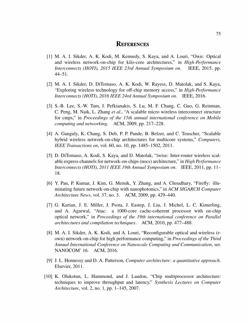
75
References
[1] M. A. I. Sikder, A. K. Kodi, M. Kennedy, S. Kaya, and A. Louri, “Own: Opticaland wireless network-on-chip for kilo-core architectures,” in High-PerformanceInterconnects (HOTI), 2015 IEEE 23rd Annual Symposium on. IEEE, 2015, pp.44–51.
[2] M. A. I. Sikder, D. DiTomaso, A. K. Kodi, W. Rayess, D. Matolak, and S. Kaya,“Exploring wireless technology for off-chip memory access,” in High-PerformanceInterconnects (HOTI), 2016 IEEE 24rd Annual Symposium on. IEEE, 2016.
[3] S.-B. Lee, S.-W. Tam, I. Pefkianakis, S. Lu, M. F. Chang, C. Guo, G. Reinman,C. Peng, M. Naik, L. Zhang et al., “A scalable micro wireless interconnect structurefor cmps,” in Proceedings of the 15th annual international conference on Mobilecomputing and networking. ACM, 2009, pp. 217–228.
[4] A. Ganguly, K. Chang, S. Deb, P. P. Pande, B. Belzer, and C. Teuscher, “Scalablehybrid wireless network-on-chip architectures for multicore systems,” Computers,IEEE Transactions on, vol. 60, no. 10, pp. 1485–1502, 2011.
[5] D. DiTomaso, A. Kodi, S. Kaya, and D. Matolak, “iwise: Inter-router wireless scal-able express channels for network-on-chips (nocs) architecture,” in High PerformanceInterconnects (HOTI), 2011 IEEE 19th Annual Symposium on. IEEE, 2011, pp. 11–18.
[6] Y. Pan, P. Kumar, J. Kim, G. Memik, Y. Zhang, and A. Choudhary, “Firefly: illu-minating future network-on-chip with nanophotonics,” in ACM SIGARCH ComputerArchitecture News, vol. 37, no. 3. ACM, 2009, pp. 429–440.
[7] G. Kurian, J. E. Miller, J. Psota, J. Eastep, J. Liu, J. Michel, L. C. Kimerling,and A. Agarwal, “Atac: a 1000-core cache-coherent processor with on-chipoptical network,” in Proceedings of the 19th international conference on Parallelarchitectures and compilation techniques. ACM, 2010, pp. 477–488.
[8] M. A. I. Sikder, A. K. Kodi, and A. Louri, “Reconfigurable optical and wireless (r-own) network-on-chip for high performance computing,” in Proceedings of the ThirdAnnual International Conference on Nanoscale Computing and Communication, ser.NANOCOM’ 16. ACM, 2016.
[9] J. L. Hennessy and D. A. Patterson, Computer architecture: a quantitative approach.Elsevier, 2011.
[10] K. Olukotun, L. Hammond, and J. Laudon, “Chip multiprocessor architecture:techniques to improve throughput and latency,” Synthesis Lectures on ComputerArchitecture, vol. 2, no. 1, pp. 1–145, 2007.
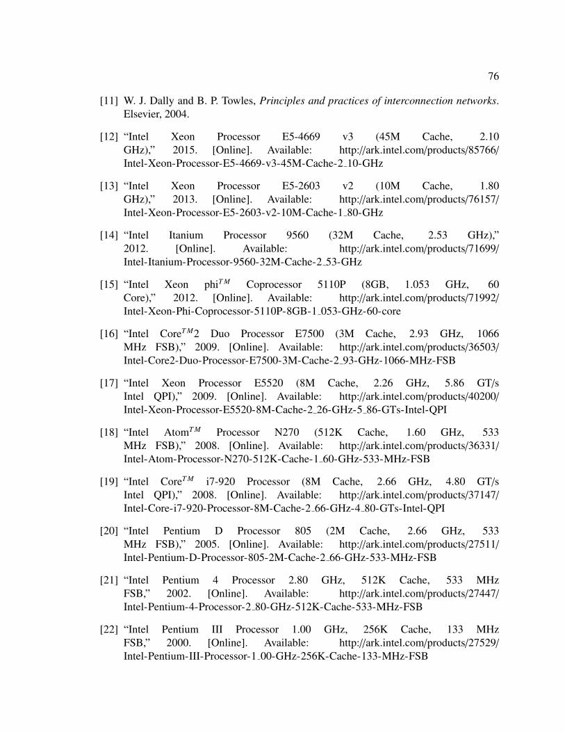
76
[11] W. J. Dally and B. P. Towles, Principles and practices of interconnection networks.Elsevier, 2004.
[12] “Intel Xeon Processor E5-4669 v3 (45M Cache, 2.10GHz),” 2015. [Online]. Available: http://ark.intel.com/products/85766/
Intel-Xeon-Processor-E5-4669-v3-45M-Cache-2 10-GHz
[13] “Intel Xeon Processor E5-2603 v2 (10M Cache, 1.80GHz),” 2013. [Online]. Available: http://ark.intel.com/products/76157/
Intel-Xeon-Processor-E5-2603-v2-10M-Cache-1 80-GHz
[14] “Intel Itanium Processor 9560 (32M Cache, 2.53 GHz),”2012. [Online]. Available: http://ark.intel.com/products/71699/
Intel-Itanium-Processor-9560-32M-Cache-2 53-GHz
[15] “Intel Xeon phiT M Coprocessor 5110P (8GB, 1.053 GHz, 60Core),” 2012. [Online]. Available: http://ark.intel.com/products/71992/
Intel-Xeon-Phi-Coprocessor-5110P-8GB-1 053-GHz-60-core
[16] “Intel CoreT M2 Duo Processor E7500 (3M Cache, 2.93 GHz, 1066MHz FSB),” 2009. [Online]. Available: http://ark.intel.com/products/36503/
Intel-Core2-Duo-Processor-E7500-3M-Cache-2 93-GHz-1066-MHz-FSB
[17] “Intel Xeon Processor E5520 (8M Cache, 2.26 GHz, 5.86 GT/sIntel QPI),” 2009. [Online]. Available: http://ark.intel.com/products/40200/
Intel-Xeon-Processor-E5520-8M-Cache-2 26-GHz-5 86-GTs-Intel-QPI
[18] “Intel AtomT M Processor N270 (512K Cache, 1.60 GHz, 533MHz FSB),” 2008. [Online]. Available: http://ark.intel.com/products/36331/
Intel-Atom-Processor-N270-512K-Cache-1 60-GHz-533-MHz-FSB
[19] “Intel CoreT M i7-920 Processor (8M Cache, 2.66 GHz, 4.80 GT/sIntel QPI),” 2008. [Online]. Available: http://ark.intel.com/products/37147/
Intel-Core-i7-920-Processor-8M-Cache-2 66-GHz-4 80-GTs-Intel-QPI
[20] “Intel Pentium D Processor 805 (2M Cache, 2.66 GHz, 533MHz FSB),” 2005. [Online]. Available: http://ark.intel.com/products/27511/
Intel-Pentium-D-Processor-805-2M-Cache-2 66-GHz-533-MHz-FSB
[21] “Intel Pentium 4 Processor 2.80 GHz, 512K Cache, 533 MHzFSB,” 2002. [Online]. Available: http://ark.intel.com/products/27447/
Intel-Pentium-4-Processor-2 80-GHz-512K-Cache-533-MHz-FSB
[22] “Intel Pentium III Processor 1.00 GHz, 256K Cache, 133 MHzFSB,” 2000. [Online]. Available: http://ark.intel.com/products/27529/
Intel-Pentium-III-Processor-1 00-GHz-256K-Cache-133-MHz-FSB
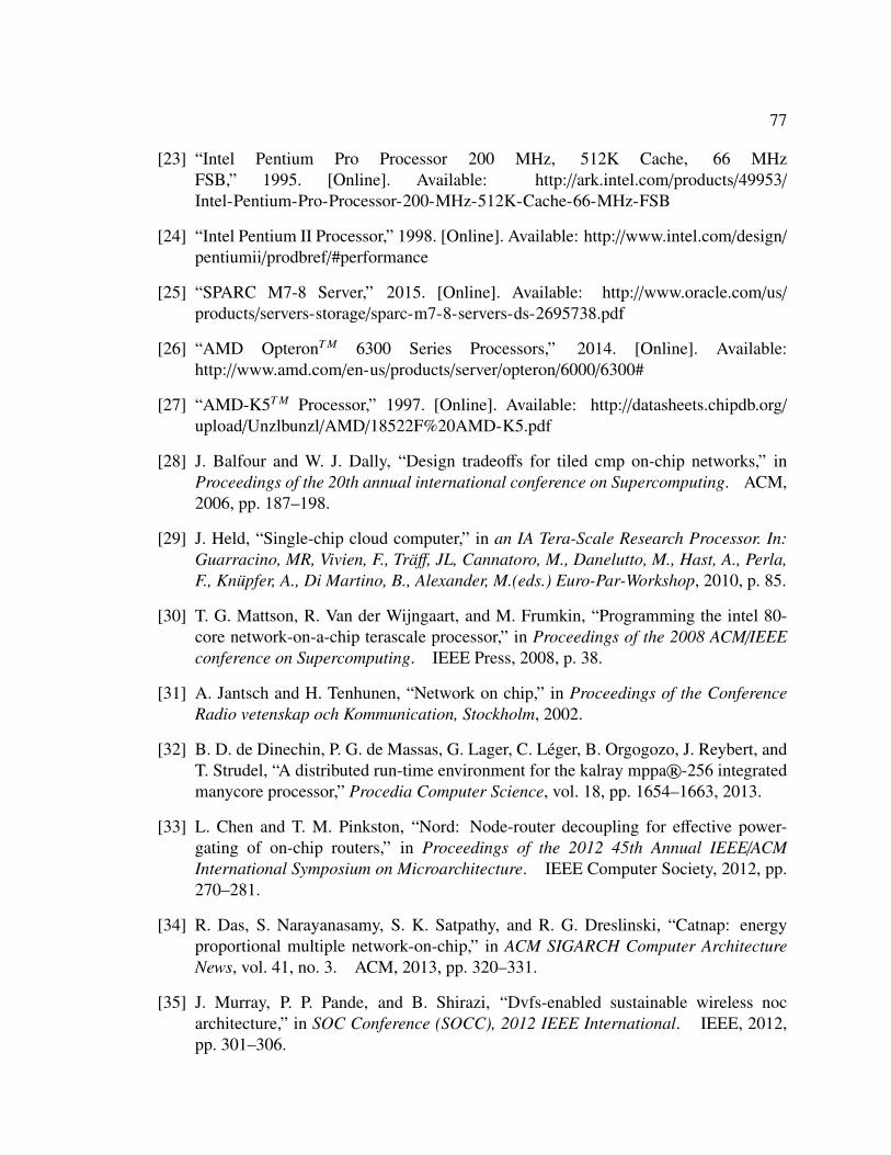
77
[23] “Intel Pentium Pro Processor 200 MHz, 512K Cache, 66 MHzFSB,” 1995. [Online]. Available: http://ark.intel.com/products/49953/
Intel-Pentium-Pro-Processor-200-MHz-512K-Cache-66-MHz-FSB
[24] “Intel Pentium II Processor,” 1998. [Online]. Available: http://www.intel.com/design/
pentiumii/prodbref/#performance
[25] “SPARC M7-8 Server,” 2015. [Online]. Available: http://www.oracle.com/us/products/servers-storage/sparc-m7-8-servers-ds-2695738.pdf
[26] “AMD OpteronT M 6300 Series Processors,” 2014. [Online]. Available:http://www.amd.com/en-us/products/server/opteron/6000/6300#
[27] “AMD-K5T M Processor,” 1997. [Online]. Available: http://datasheets.chipdb.org/
upload/Unzlbunzl/AMD/18522F%20AMD-K5.pdf
[28] J. Balfour and W. J. Dally, “Design tradeoffs for tiled cmp on-chip networks,” inProceedings of the 20th annual international conference on Supercomputing. ACM,2006, pp. 187–198.
[29] J. Held, “Single-chip cloud computer,” in an IA Tera-Scale Research Processor. In:Guarracino, MR, Vivien, F., Traff, JL, Cannatoro, M., Danelutto, M., Hast, A., Perla,F., Knupfer, A., Di Martino, B., Alexander, M.(eds.) Euro-Par-Workshop, 2010, p. 85.
[30] T. G. Mattson, R. Van der Wijngaart, and M. Frumkin, “Programming the intel 80-core network-on-a-chip terascale processor,” in Proceedings of the 2008 ACM/IEEEconference on Supercomputing. IEEE Press, 2008, p. 38.
[31] A. Jantsch and H. Tenhunen, “Network on chip,” in Proceedings of the ConferenceRadio vetenskap och Kommunication, Stockholm, 2002.
[32] B. D. de Dinechin, P. G. de Massas, G. Lager, C. Leger, B. Orgogozo, J. Reybert, andT. Strudel, “A distributed run-time environment for the kalray mppa®-256 integratedmanycore processor,” Procedia Computer Science, vol. 18, pp. 1654–1663, 2013.
[33] L. Chen and T. M. Pinkston, “Nord: Node-router decoupling for effective power-gating of on-chip routers,” in Proceedings of the 2012 45th Annual IEEE/ACMInternational Symposium on Microarchitecture. IEEE Computer Society, 2012, pp.270–281.
[34] R. Das, S. Narayanasamy, S. K. Satpathy, and R. G. Dreslinski, “Catnap: energyproportional multiple network-on-chip,” in ACM SIGARCH Computer ArchitectureNews, vol. 41, no. 3. ACM, 2013, pp. 320–331.
[35] J. Murray, P. P. Pande, and B. Shirazi, “Dvfs-enabled sustainable wireless nocarchitecture,” in SOC Conference (SOCC), 2012 IEEE International. IEEE, 2012,pp. 301–306.
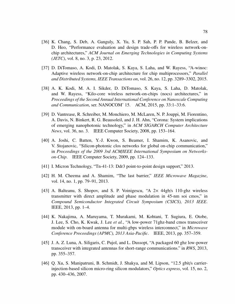
78
[36] K. Chang, S. Deb, A. Ganguly, X. Yu, S. P. Sah, P. P. Pande, B. Belzer, andD. Heo, “Performance evaluation and design trade-offs for wireless network-on-chip architectures,” ACM Journal on Emerging Technologies in Computing Systems(JETC), vol. 8, no. 3, p. 23, 2012.
[37] D. DiTomaso, A. Kodi, D. Matolak, S. Kaya, S. Laha, and W. Rayess, “A-winoc:Adaptive wireless network-on-chip architecture for chip multiprocessors,” Paralleland Distributed Systems, IEEE Transactions on, vol. 26, no. 12, pp. 3289–3302, 2015.
[38] A. K. Kodi, M. A. I. Sikder, D. DiTomaso, S. Kaya, S. Laha, D. Matolak,and W. Rayess, “Kilo-core wireless network-on-chips (nocs) architectures,” inProceedings of the Second Annual International Conference on Nanoscale Computingand Communication, ser. NANOCOM’ 15. ACM, 2015, pp. 33:1–33:6.
[39] D. Vantrease, R. Schreiber, M. Monchiero, M. McLaren, N. P. Jouppi, M. Fiorentino,A. Davis, N. Binkert, R. G. Beausoleil, and J. H. Ahn, “Corona: System implicationsof emerging nanophotonic technology,” in ACM SIGARCH Computer ArchitectureNews, vol. 36, no. 3. IEEE Computer Society, 2008, pp. 153–164.
[40] A. Joshi, C. Batten, Y.-J. Kwon, S. Beamer, I. Shamim, K. Asanovic, andV. Stojanovic, “Silicon-photonic clos networks for global on-chip communication,”in Proceedings of the 2009 3rd ACM/IEEE International Symposium on Networks-on-Chip. IEEE Computer Society, 2009, pp. 124–133.
[41] I. Micron Technology, “Tn-41-13: Ddr3 point-to-point design support,” 2013.
[42] H. M. Cheema and A. Shamim, “The last barrier,” IEEE Microwave Magazine,vol. 14, no. 1, pp. 79–91, 2013.
[43] A. Balteanu, S. Shopov, and S. P. Voinigescu, “A 2× 44gb/s 110-ghz wirelesstransmitter with direct amplitude and phase modulation in 45-nm soi cmos,” inCompound Semiconductor Integrated Circuit Symposium (CSICS), 2013 IEEE.IEEE, 2013, pp. 1–4.
[44] K. Nakajima, A. Maruyama, T. Murakami, M. Kohtani, T. Sugiura, E. Otobe,J. Lee, S. Cho, K. Kwak, J. Lee et al., “A low-power 71ghz-band cmos transceivermodule with on-board antenna for multi-gbps wireless interconnect,” in MicrowaveConference Proceedings (APMC), 2013 Asia-Pacific. IEEE, 2013, pp. 357–359.
[45] J. A. Z. Luna, A. Siligaris, C. Pujol, and L. Dussopt, “A packaged 60 ghz low-powertransceiver with integrated antennas for short-range communications.” in RWS, 2013,pp. 355–357.
[46] Q. Xu, S. Manipatruni, B. Schmidt, J. Shakya, and M. Lipson, “12.5 gbit/s carrier-injection-based silicon micro-ring silicon modulators,” Optics express, vol. 15, no. 2,pp. 430–436, 2007.
79
[47] D. Abts, N. D. Enright Jerger, J. Kim, D. Gibson, and M. H. Lipasti, “Achievingpredictable performance through better memory controller placement in many-corecmps,” in ACM SIGARCH Computer Architecture News, vol. 37, no. 3. ACM, 2009,pp. 451–461.
[48] A. Sharifi, E. Kultursay, M. Kandemir, and C. Das, “Addressing end-to-end memoryaccess latency in noc-based multicores,” in Microarchitecture (MICRO), 2012 45thAnnual IEEE/ACM International Symposium on, Dec 2012, pp. 294–304.
[49] C. Sun, C.-H. Chen, G. Kurian, L. Wei, J. Miller, A. Agarwal, L.-S. Peh, andV. Stojanovic, “Dsent-a tool connecting emerging photonics with electronics for opto-electronic networks-on-chip modeling,” in Networks on Chip (NoCS), 2012 SixthIEEE/ACM International Symposium on. IEEE, 2012, pp. 201–210.
[50] A. Kodi and A. Louri, “A system simulation methodology of optical interconnects forhigh-performance computing systems,” J. Opt. Netw, vol. 6, no. 12, pp. 1282–1300,2007.
[51] J. Kim, W. J. Dally, B. Towles, and A. K. Gupta, “Microarchitecture of a high-radixrouter,” in ACM SIGARCH Computer Architecture News, vol. 33, no. 2. IEEEComputer Society, 2005, pp. 420–431.
[52] R. Ubal, J. Sahuquillo, S. Petit, P. Lopez, Z. Chen, and D. R. Kaeli, “The multi2simsimulation framework: A cpu-gpu model for heterogeneous computing,” 2011.
[53] C. Bienia, S. Kumar, J. P. Singh, and K. Li, “The parsec benchmark suite: Char-acterization and architectural implications,” in Proceedings of the 17th internationalconference on Parallel architectures and compilation techniques. ACM, 2008, pp.72–81.
[54] I. Bhati, Z. Chishti, S.-L. Lu, and B. Jacob, “Flexible auto-refresh: Enabling scalableand energy-efficient dram refresh reductions,” in Computer Architecture (ISCA), 2015ACM/IEEE 42nd Annual International Symposium on, June 2015, pp. 235–246.
[55] J. Ahn, S. Yoo, O. Mutlu, and K. Choi, “Pim-enabled instructions: A low-overhead,locality-aware processing-in-memory architecture,” in Computer Architecture (ISCA),2015 ACM/IEEE 42nd Annual International Symposium on, June 2015, pp. 336–348.
[56] Y. Lee, J. Kim, H. Jang, H. Yang, J. Kim, J. Jeong, and J. Lee, “A fully associative,tagless dram cache,” in Computer Architecture (ISCA), 2015 ACM/IEEE 42nd AnnualInternational Symposium on, June 2015, pp. 211–222.
[57] O. Seongil, Y. H. Son, N. S. Kim, and J. H. Ahn, “Row-buffer decoupling: Acase for low-latency dram microarchitecture,” in Computer Architecture (ISCA), 2014ACM/IEEE 41st International Symposium on, June 2014, pp. 337–348.
80
[58] A. Ros and S. Kaxiras, “Callback: Efficient synchronization without invalidation witha directory just for spin-waiting,” in Computer Architecture (ISCA), 2015 ACM/IEEE42nd Annual International Symposium on, June 2015, pp. 427–438.
[59] L. Peled, S. Mannor, U. Weiser, and Y. Etsion, “Semantic locality and context-basedprefetching using reinforcement learning,” in Computer Architecture (ISCA), 2015ACM/IEEE 42nd Annual International Symposium on, June 2015, pp. 285–297.

!!!!!!!!!!!!!!!!!!!!!!!!!!!!!!!!!!!!!!!
!!
Thesis and Dissertation Services