silicon photomultiplier characterization - uva · peter lyle rossiter 28/9/2015 master thesis...
TRANSCRIPT

Silicon Photomultiplier
Characterization
Peter Lyle Rossiter
28/9/2015
Master Thesis
Supervisor: David Berge
Examiners: David Berge and Niels van Bakel

Abstract
The Cherenkov Telescope Array (CTA) is a next generation ImagingAir Cherenkov Telescope (IACT) and is being built to examine cosmicgamma-rays from below ∼100 GeV to above ∼100 TeV. Within thisarray a Small Size Telescope (SST) is being developed to lookspeci�cally at gamma-rays in the range of ∼10 TeV to ∼100 TeV (VHEgamma-rays). In order to record gamma-ray events the SST will collectCherenkov light from the relativistic secondary particles generated bythe extended air shower seen when VHE gamma-rays interact in ouratmosphere. This will require a camera sensitive to blue and ultra violetlight characteristic of Cherenkov radiation; a role which will be �lled bythe Compact High Energy Camera (CHEC).One of the targets of the CHEC collaboration is to develop a prototypecamera with a photosensitive layer comprised of Silicon Photomultipliers(SiPMs); a relatively new technology developed to replace the role ofPMTs in the current generation of IACTs. SiPMs are an attractiveoption as they have an improved photo-sensitivity and time resolutioncompared to PMTs, and deliver this at a cheaper cost in a more robustunit. The size of SiPMs in particular will a�ord CTA never before seenresolution leading to potentially ∼1000 TeV sources being pinpointed onthe night sky. In order to facilitate this, the experimental setup atNIKHEF will be developed to characterize SiPMs. This development willallow devices to be assessed and compared for suitability within CHEC.The goal of this thesis was to develop the existing experimental setup forSiPM characterization at NIKHEF. By ensuring the apparatus was lighttight, and that sensor temperature could be controlled, the setup oughtto become appropriate for assessing dark count rate (DCR), dynamicrange (DR), photon detection e�ciency (PDE), single photo-equivalentpulse (1 PE) level and crosstalk probability. With this setup in hand,two potential SiPM arrays, the Philips Digital Photon Counting kit(PDPC) and the Excelitas C30742-66 Series SiPM, were tested andcompared for suitability in CHEC.The results of this analysis showed that after developing the apparatus,it went from not being light tight, to light tight with a con�dence of α =0.01, and temperature controlled to within2.22×10−4 ◦K
s±1.11×10⁻⁴ ◦K
s. This allowed for the determination of
several SiPM characteristics for comparison. The results also showedthat the DCR and crosstalk probability for both devices under test werecomparable. However, the Excelitas sample crucially outperforms thePDPC with respect to its dynamic range. While the PDPC dynamicrange peaks at a cell breakdown rate of ∼44 MHz/cm2, the Excelitassample showed no sign of saturation at the same light level. Thismeasure rules out the PDPC for use in CHEC as the expectedbackground cell breakdown rate from the current HESS data is ∼100MHz/cm2.
I

Contents
1 Introduction 1
2 Very High Energy Gamma-Ray Astronomy 12.1 Very High Energy Gamma-Ray Astronomy . . . . . . . . . . . . 22.2 Gamma-Ray Production . . . . . . . . . . . . . . . . . . . . . . . 22.3 Imaging Atmospheric Cherenkov Telescopes . . . . . . . . . . . . 62.4 The Cherenkov Telescope Array . . . . . . . . . . . . . . . . . . . 72.5 The Compact High Energy Camera . . . . . . . . . . . . . . . . . 8
3 The Silicon Photomultiplier 93.1 Photon Detection . . . . . . . . . . . . . . . . . . . . . . . . . . . 103.2 The Silicon Photomultiplier . . . . . . . . . . . . . . . . . . . . . 123.3 Over Voltage . . . . . . . . . . . . . . . . . . . . . . . . . . . . . 123.4 Noise . . . . . . . . . . . . . . . . . . . . . . . . . . . . . . . . . . 12
3.4.1 Thermal Noise . . . . . . . . . . . . . . . . . . . . . . . . 133.4.2 Optical Crosstalk . . . . . . . . . . . . . . . . . . . . . . . 133.4.3 After Pulses . . . . . . . . . . . . . . . . . . . . . . . . . . 14
3.5 Gain . . . . . . . . . . . . . . . . . . . . . . . . . . . . . . . . . . 143.6 Dynamic Range . . . . . . . . . . . . . . . . . . . . . . . . . . . . 143.7 Quantum E�ciency . . . . . . . . . . . . . . . . . . . . . . . . . 143.8 Photon Detection E�ciency . . . . . . . . . . . . . . . . . . . . . 143.9 Pulse Shape . . . . . . . . . . . . . . . . . . . . . . . . . . . . . . 153.10 CHEC Requirements . . . . . . . . . . . . . . . . . . . . . . . . . 15
4 Preliminary Setup Analysis 164.1 The Kolmogorov Smirnov Test . . . . . . . . . . . . . . . . . . . 164.2 Apparatus . . . . . . . . . . . . . . . . . . . . . . . . . . . . . . . 17
4.2.1 The Philips Digital Photon Counter . . . . . . . . . . . . 184.3 Procedure . . . . . . . . . . . . . . . . . . . . . . . . . . . . . . . 19
4.3.1 Light tightness and temperature control . . . . . . . . . . 194.3.2 Dynamic Range Test . . . . . . . . . . . . . . . . . . . . . 20
4.4 Discussion . . . . . . . . . . . . . . . . . . . . . . . . . . . . . . . 214.5 Conclusion and Recommendations . . . . . . . . . . . . . . . . . 25
5 Setup Development 265.1 Temperature Control . . . . . . . . . . . . . . . . . . . . . . . . . 26
5.1.1 Apparatus . . . . . . . . . . . . . . . . . . . . . . . . . . . 26Peltier Element . . . . . . . . . . . . . . . . . . . . . . . 27
5.1.2 Procedure . . . . . . . . . . . . . . . . . . . . . . . . . . . 275.1.3 Discussion . . . . . . . . . . . . . . . . . . . . . . . . . . . 275.1.4 Conclusion . . . . . . . . . . . . . . . . . . . . . . . . . . 28
5.2 Light Tightness . . . . . . . . . . . . . . . . . . . . . . . . . . . . 295.2.1 Procedure . . . . . . . . . . . . . . . . . . . . . . . . . . . 295.2.2 Discussion . . . . . . . . . . . . . . . . . . . . . . . . . . . 30
II

5.2.3 Conclusion . . . . . . . . . . . . . . . . . . . . . . . . . . 305.3 LED Attenuation . . . . . . . . . . . . . . . . . . . . . . . . . . . 305.4 Updated Apparatus . . . . . . . . . . . . . . . . . . . . . . . . . 31
5.4.1 Excelitas C30742-66 Series . . . . . . . . . . . . . . . . . . 32
6 Silicon Photomultiplier Characterization 326.1 Dark Count Map . . . . . . . . . . . . . . . . . . . . . . . . . . . 32
6.1.1 Procedure . . . . . . . . . . . . . . . . . . . . . . . . . . . 336.1.2 Discussion . . . . . . . . . . . . . . . . . . . . . . . . . . . 336.1.3 Conclusion . . . . . . . . . . . . . . . . . . . . . . . . . . 34
6.2 Temperature vs. Dark Count Rate . . . . . . . . . . . . . . . . . 346.2.1 Procedure . . . . . . . . . . . . . . . . . . . . . . . . . . . 366.2.2 Discussion . . . . . . . . . . . . . . . . . . . . . . . . . . . 366.2.3 Conclusion . . . . . . . . . . . . . . . . . . . . . . . . . . 38
6.3 Dynamic Range . . . . . . . . . . . . . . . . . . . . . . . . . . . . 386.3.1 Apparatus . . . . . . . . . . . . . . . . . . . . . . . . . . . 396.3.2 Procedure . . . . . . . . . . . . . . . . . . . . . . . . . . . 406.3.3 Discussion . . . . . . . . . . . . . . . . . . . . . . . . . . . 416.3.4 Conclusion . . . . . . . . . . . . . . . . . . . . . . . . . . 44
6.4 Wavelength vs. Photon Detection E�ciency . . . . . . . . . . . . 456.4.1 Procedure . . . . . . . . . . . . . . . . . . . . . . . . . . . 466.4.2 Discussion . . . . . . . . . . . . . . . . . . . . . . . . . . . 496.4.3 Conclusion . . . . . . . . . . . . . . . . . . . . . . . . . . 51
6.5 Multi Photo-Equivalent Peak Spectrum . . . . . . . . . . . . . . 516.5.1 Apparatus . . . . . . . . . . . . . . . . . . . . . . . . . . . 526.5.2 Procedure . . . . . . . . . . . . . . . . . . . . . . . . . . . 536.5.3 Discussion . . . . . . . . . . . . . . . . . . . . . . . . . . . 536.5.4 Conclusion . . . . . . . . . . . . . . . . . . . . . . . . . . 54
7 Conclusion 557.1 Silicon Photomultiplier Comparison . . . . . . . . . . . . . . . . 557.2 Setup Development and Recommendations . . . . . . . . . . . . . 56
8 Acknowledgements 59
III

1 Introduction
This thesis will explore silicon photomultiplier characterization and the devel-opment of the experimental setup to perform said characterization. This studyis being done in conjunction with the Cherenkov Telescope Array (CTA) collab-oration; a next generation Imagine Air Cherenkov Telescope (IACT). As partof this telescope array will be Small Sized Telescopes (SSTs) used to sensitivelymeasure cosmic gamma-ray �uxes above ∼10 TeV. An essential component tothe SST is the Compact High Energy Camera (CHEC) which will be used todetect photons. It is the goal of the CHEC project to develop a camera whichutilises the new technology of Silicon Photomultipliers (SiPMs). It is hopedthese devices will improved collection rates. [1] [3].What is of particular focus for this thesis is the development of the experimentalsetup at NIKHEF to characterize SiPMs. Several characteristics are of speci�cattention to this study, these are; dark count rate, dynamic range, photon de-tection e�ciency, the single photo-equivalent peak and crosstalk probability. Todo this it will �rst be necessary to ensure that the apparatus has su�cient tem-perature control, is light tight and that the optical power of light emitting diodeused to test the devices is operating in a range appropriate to the devices undertest. All three of these variables can a�ect cell break down rates, making themconfounding variables when determining true photon count rates.With this improved experimental apparatus, characterization of two devices wasconducted. Speci�cally the devices examined were the Philips Digital PhotonCounting Kit [16], and the Excelitas C30742-66 Series SiPM [27]. In the endthese two devices were compared for their suitability for use within the CHECcamera.Chapter 2 of this thesis will begin by discussing very high energy astronomyChapter 3 will go on to discuss silicon photomultipliers. Chapter 4 will examinethe existing setup at NIKHEF and motivate any developments which need tobe made. Chapter 5 will explain setup developments which needed to occur.Chapter 6 will detail the SiPM characterization which was performed. To con-clude characteristics of both SiPMs under test will be examined and compared,followed by a recommendation for which of the two will be the better option forthe CHEC camera.
2 Very High Energy Gamma-Ray Astronomy
In this section I will introduce Very High Energy (VHE) Gamma-Ray Astron-omy, Imaging Atmospheric Cherenkov Telescopes (IACTs), the Cherenkov Tele-scope Array (CTA) and the Compact High Energy Camera (CHEC). This sec-tion will conclude by focusing on the photo-sensors of the CHEC. Unless other-wise speci�ed, all material is based on [1], [2] and [3].
1

2.1 Very High Energy Gamma-Ray Astronomy
A relatively recent development in the �eld of astronomy is the study of veryhigh energy gamma-rays. By observing VHE gamma-rays (i.e. with energy >10 GeV) we are given a window into the most extreme astrophysical processesin the Universe. A more exciting notion comes from the fact there is no knownway for thermal radiation to have the actual energy observed in VHE gamma-rays. These gamma-rays are thought to be the result acceleration of relativisticcharged particles, for example by a magnetic �eld or a plasma shock. Thus thepowerful processes behind their origins could provide a window to examine the-ories beyond the standard model. The list of possible candidates for sources ofVHE gamma-rays is wide open but includes collapsed stars and super massiveblack holes.Furthermore VHE gamma-ray astronomy will continue to �nd itself at the fore-front of physics for some time as it is theorized that gamma-rays could be by-products of new physical processes, such as neutralino annihilation. Thus detec-tion of gamma-rays by specialised instruments such as the upcoming CherenkovTelescope Array has the potential to con�rm the existence of such processes.
2.2 Gamma-Ray Production
Stars are able to emit light because they have very high temperatures; thistype of light is known as thermal radiation. Thermal radiation has a signaturespectrum whereby the temperature of an object entirely determines its thermalradiation output. But regardless of an objects temperature it will never pro-duce a large number of gamma-rays. The abundance of gamma-rays detectedin our Universe can only be accounted for by non-thermal processes such assynchrotron radiation, bremsstrahlung radiation, inverse Compton scattering,neutral pion decay, matter/anti-matter annihilation, and nuclear transforma-tions.These e�ects are thought to occur at sources such as supernovae remnants(SNR), fast rotational objects such as neutron stars and pulsars, active galacticnuclei (AGN), and matter accreting black holes.
Synchrotron Radiation
When a charged particle changes direction in a magnetic �eld an accelerationoccurs resulting in a radiated electromagnetic (EM) wave. This EM wave isknown as Synchrotron radiation (�gure 1).Synchrotron photons have a continuous energy spectrum. Electrons with en-ergy E in a magnetic �eld of strength B radiate a power P. This relationship isre�ected in equation 1.
P ∼ E2B2 (1)
2

Figure 1: Production of synchrotron radiation due to a de�ected charged particlein a magnetic �eld.
Bremsstrahlung RadiationSimilar to synchrotron radiation, when charged particles are de�ected in aCoulomb �eld of another charge (be it an atomic nucleus or an electron) theresult is the emission of bremsstrahlung photons (�gure 2). The probability ofbremsstrahlung (φ) depends in both the square of the projectile charge (z) andthe square of the target charge (Z). φ is proportional to the particle energy,and inversely proportional to square mass of the de�ected particle. This can beseen in equation 2.
φ ∼ z2Z2E
m2(2)
Since electrons have a tiny mass compared to even the smallest atomic nuclei,they are the predominant source of bremsstrahlung photons. The bremsstrahlungphoton energy spectrum is continuous and decreases by 1/Eγ to high energies.
Figure 2: A de�ected charged particle in the Coulomb �eld of a nucleus leadingbremsstrahlung production.
Inverse Compton ScatteringCompton scattering occurs in a collision between a free electron and an energeticphoton, and is de�ned by the photon losing a percentage of its energy to theelectron. The reverse is also possible and is a signi�cant e�ect in astrophysics(�gure 3). Energetic electrons have the opportunity to collide with many pho-tons from blackbody radiation (Eγ ' 250 µeV, photon density Nγ ' 400/cm3)or starlight photons (Eγ ' 1 eV, Nγ ' 1/cm3) transferring it's energy to the
3

photon.
Figure 3: Collision of an energetic electron and a low energy photon. Theelectron transfers energy to the photon and subsequently slows down. Thephoton on the other hand gains energy and becomes blue-shifted.
Neutral Pion DecayAccelerated protons can produce charged and neutral pions in proton-protonor proton-nucleus interactions (�gure 4). A possible process for this is given inequation 3.
p+ nucleus → p'+ nucleus'+ π+ + π− + π0 (3)
The charged pions quickly decay (τ = 26 ns) into muons and neutrinos whilethe neutral pion decays (τ = 8.4× 10⁻¹⁷ s) into two photons.The division of energy between these two photons depends on the pion's motion.If it is at rest, the photons are produced back-to-back with each receiving halfthe rest mass of the pion. (∼135 MeV). In other cases it will depend on thedirection of photon emission with respect to pion direction.
Figure 4: Neutral pion production via proton interactions, followed by piondecay into photons.
4

Photons from matter / anti-matter annihilationCharged particles can annihilate with their antiparticles into energy. This pri-marily occurs via electron-positron and proton-antiproton annihilations (�gure5). A minimum of two photons must be created in this process in order to con-serve momentum. In the rest frame of e+e− annihilation each photon receives511 keV; equivalent to the rest mass of the electron and positron respectively.This process can also occur between a proton and anti-proton to produce aneutral pion. This process can be seen in equation 4, where the neutral pionsubsequently decays into two photons.
p+ + p− → π+ + π− + π0 (4)
Figure 5: e+e− annihilation into two photons.
Photons from Nuclear TransformationsSupernova explosions result in the production of heavy elements, leading toboth stable elements and radioactive isotopes. As a result of beta decay theseisotopes emit photons in the MeV range. An example of this can be seen inequation 5.
⇒60 Co →60 Ni∗∗ + e− + νe
⇒60 Ni∗∗ →60 Ni∗ + γ (1.17 MeV)
⇒60 Ni∗ →60 Ni+ γ (1.33 MeV)
(5)
Neutralino AnnihilationNeutralinos are an exotic particle from beyond the standard model. They existas the super-symmetric partner to neutrinos. In certain situations it is theorizedthat the annihilation of neutralinos could result in the production of photons.This annihilation can be seen in equation 6.
χ+ χ = γ + γ (6)
5

2.3 Imaging Atmospheric Cherenkov Telescopes
With the exceptions of radio waves and visible light, electromagnetic (EM) ra-diation arriving at Earth will not be able to pass through our atmosphere toground level (see Figure 6). In order to observe radiation of other wavelengthit has traditionally been required to take measurements at high altitudes withthe aid of balloons and other aircraft. More recently, mounting instrumentson satellites has been possible. But such techniques present another problemfor VHE gamma-ray astronomy as there are typically very low �uxes (∼ a fewphotons per m2 per year) coming from objects of astro-physical interest. Thusany sensor mounted on a satellite, hampered with a low collection area, cannotbe expected to provide much data.
Figure 6: Earth's atmosphere stops most EM radiation from reaching the sur-face. This illustration shows the atmospheric penetration depth of di�erentparts of the EM spectrum before absorption. [4]
However when VHE gamma-rays interact with nuclei in the atmosphere theycreate particle cascades (a.k.a. extensive air showers), and in this we �nd asolution to our detection problem. Detection becomes possible because the rel-ativistic secondary particles in air showers move faster than the local speed oflight, resulting in the emission of Cherenkov light. This light can be thought ofas the counterpart to the shock wave created by objects moving at supersonicspeeds. This Cherenkov radiation appears as blue or UV light, emanating ina narrow cone around the path of the original gamma-rays. This allows theCherenkov light to be used to "reconstruct" the direction and energy of theoriginal gamma-ray (�gure 7).In Imaging Atmospheric Cherenkov Telescopes (IACTs), collected Cherenkovlight is focused into a camera consisting of an array of light sensitive photomul-
6

tipliers, facilitating the generation of an image of the air shower (see Figure 7).Because the "light pool" of these showers is large at ground level, the energy ofshower is spread out over a wider area. Thus the detection surface must also belarge (of order 105 m2).
Figure 7: An extended air shower where a primary gamma-ray produces manysecondary particles. Illustration also includes the associated Cherenkov lightwhen the charged relativistic secondary particles are travelling faster than thelocal speed of light, speci�cally showing how this Cherenkov light cone fallsaround a given detection area. Finally the illustration shows how a given photondetection from a Cherenkov cone is recorded on the pixels of a telescope camera.
2.4 The Cherenkov Telescope Array
The soon to be built Cherenkov Telescope Array (CTA) is an example of anext generation IACT. The CTA is designed to observe VHE gamma-rays fromastrophysical sources. It is envisaged as an open observatory made up of twoarrays of IACTs, one in each hemisphere, for full sky coverage. The northernsite will be in located in La Palma (consisting of ∼19 dishes) and will focuson low energy extra galactic objects only. The southern site will be located inParanal Chile (∼99 dishes), and will focus on galactic and extra-galactic objectsacross the full energy range. Both sites will be jointly constructed and operatedby one international consortium.While Modern IACTs (HESS, MAGIC and VERITAS) have taken great stridesin ground based gamma-ray astronomy above ∼10 GeV and the investigation ofcosmic non-thermal processes, CTA will be building on this work in ways notpreviously possible. The current accessible energy range by modern IACTs is∼50 GeV to ∼50 TeV. Not only will CTA extend this accessible energy range(from below ∼50 GeV to above ∼100 TeV), it will also increasing the sensitivityin the energy range of ∼100 GeV to ∼ 10 TeV by an expected factor of 5-10.Furthermore, current IACTs typically use no more than 5 telescopes; resulting
7

in most showers only being viewed by 2 or 3 telescopes. This limits the abilityto distinguish between showers that have a gamma-ray origin from those witha cosmic-ray origin 1. CTA will improve on this dramatically by increasing theobserved area. This will also provide the added bene�t of improved angularresolution due to the larger number of views of each cascade.The improved angular resolution of CTA will for the �rst time allow us toresolve between structures of Galactic emission regions on parsec scales. It isexpected that CTA will pin-point more than 1000 TeV, galactic, and extra-galactic gamma-ray sources. This would increase previous levels of detection bya factor of > 10.
2.5 The Compact High Energy Camera
CTA is envisaged as employing three types of telescopes; Large-Sized Telescopes(LSTs), Medium-Sized Telescopes (MSTs) and Small-Sized Telescopes (SSTs).The SSTs are intended to be sparsely arrayed with large �elds of view. Theirpurpose is to detect the highest energy gamma-rays, which are typically bright,and spread over a large area but are relatively rare events. The Compact HighEnergy Camera (CHEC) project has been speci�cally set up to meet these de-mands.
Figure 8: The CHEC. This version is equipped with MAPMs instead of SiPMs.Di�erent pre-ampli�ers are used with each sensor type to allow the use of thesubsequent electronics chain.
CHEC is to be the camera used by the SST. Two CHEC prototypes, basedon di�erent photo-sensors, are underway. CHEC-M, the �rst prototype will be
1Cherenkov showers from a cosmic-ray origin are the primary background events for VHEgamma-ray astronomy.
8

based on multi-anode photomultipliers and CHEC-S, on silicon photomultipli-ers. CHEC will be built to provide a reliable, inexpensive, quality assured solu-tion to the SST. It is to have a curved focal plane to meet the SST optical needs,and will be �tted with 32 × 64 pixel photo-sensor modules (�gure 8). Photo-sensor signals will be fed to a low noise shaping pre-ampli�er and then, to a 1GS/s (i.e. 1 ns time-bin) digitising application-speci�c integrated circuit (calledTARGET). Camera level trigger decisions will be made on a black-plane printedcircuit board (PCB) with programmable trigger algorithms implemented on a�eld programmable gate array. CHEC will give full waveforms for each camerapixel in every event.The photo-sensors to be used in this device are the focus of this thesis, speci�-cally the testing of silicon photomultipliers for the CHEC-S. In the next sectionI will describe the silicon photomultiplier, and explain what qualities make it isa good �t for the CHEC camera.
(a) SiPM array and PMT side on view. (b) SiPM array and PMT front onview.
Figure 9: The PMT is a decommissioned Hamamatsu R580 formerly from theZEUS experiment, it is 13 cm long and has a diameter of 4 cm. The SiPM arrayis the Philips DPC-6400-22 consisting of over ∼400,000 individual SiPM cells.The SiPM array has an outer dimension of 3.26 cm× 3.26 cm, with individualcells being 59.4 µm × 32 µm.
3 The Silicon Photomultiplier
Section 2 explained the need for a light sensitive device in CHEC, this chapterwill look at a device that is capable of doing that; the Silicon Photomultiplier(SiPM). SiPMs represent the next step in avalanche photodiode (APD) tech-nology [5�10]. At low temperatures SiPMs typically have an improved gain andresponse to PMTs. SiPMs also have the advantage in their compact size (�g-ure 9) and ruggedness [11]. It is these characteristics which have led to theirpotential use not only by VHE gamma-ray astronomy [3] but also medium en-
9

ergy physics, high energy physics and medical applications [12,13].Similar to a PMT, an SiPM provides high gain and a fast response when de-tecting radiation. What is particularly interesting about both these devices istheir ability to detect low levels of light, even single photons. What's more,both devices achieve this low level light detection, with high photo-sensitivityand time resolution. However SiPMs typically deliver a higher photon sensitiv-ity at a lower cost and in a more robust unit. The SiPM has a lower voltageoperation, a lower power consumption requirement, and also o�ers insensitivityto magnetic �elds. It is mechanically robust and gives highly uniform responsesto homogeneous light sources. For these reasons the SiPM is quickly becomingthe detection tool of choice in high energy physics.In this section I will discuss how an SiPM detects photons, possible sourcesof noise and important characteristics. I will �nish by discussing what theseparameters need to be for the CHEC camera.
3.1 Photon Detection
As a photon travels through silicon there is a certain probability of it transfer-ring energy to a valence electron, thus pushing it into the conduction band. Thisprocess is also known as creating an electron-hole pair. As shown in �gure 10,a photons absorption depth in silicon is dependent on its energy/ wavelength.This tells us that silicon is an excellent material for photon detection in therange from 350 nm up to 1000 nm. Below 350 nm the absorption length is soshort that silicon is too thin and above 1000 nm it is too bulky.
This e�ect can be used to detect incident light. The force which would usuallypull electrons and holes back together can be suppressed by applying a reversebias across the diode in the depleted region of a p-n junction. Such an arrange-ment will lead to a �ow of electrons to the n-type side and holes to the p-typeside of the device when the respective charge carriers are created by a photon.To understand how a depleted region in a p-n junction leads to the detectionof photons consider the case of an energetic photon passing through the regionwhich has been reversed biased. Assuming this photons energy is greater thanthe band gap energy of the material it is passing through (1.1 eV for silicon),there is a certain probability of the creation of an electron-hole (e-h) pair. Inthis case the �eld will cause the electron to move towards the n side and thehole towards the p side. In the circuit around the photodiode this will leadto the �ow of a photo-electron. These two newly created charge carriers areaccelerated until they have enough kinetic energy to create secondary pairs ofelectrons and holes. This occurs via a process known as impact ionization.Here, one photo-electron can start an ionization cascade that spreads throughthe whole silicon where ever the �eld is applied. At this point we see the siliconbreak down and become conductive, which ampli�es the original photo-electroninto a much larger current. This is called a Geiger discharge, and is illustratedin �gure 11 (a).
The gain of photodiodes in Geiger mode can be improved with the use of this
10

Figure 10: The e�ect of wavelength on photon absorption depth in silicon [14]. Anotable feature omitted from this plot is a cut-o� at ∼1115 nm as the wavelengthdrops below the band gap energy. This occurs because the photon is no longerenergetic enough to create an electron-hole-pair.
(a) A Geiger discharge in an APD. It causesan ionisation cascade in which a single pho-ton begins an chain of impact ionizationsspreading through the whole depleted region
(b) Cycle of cell breakdown, avalanche,quenching and bias reset.
Figure 11: Illustrations from [14]
11

breakdown. The p-n junction region is designed so that it is able to maintain areverse voltage bias beyond its nominal breakdown voltage, creating the large�eld gradients across the junction. Once a current is �owing then it needs tobe stopped (a.k.a. quenched). This can be done by using what is called passivequenching, (i.e. without using active circuitry). Here a series resistor (RQ)restricts the current taken by the diode as it breaks down. Subsequently, thereis a reduction in the reverse voltage seen by the diode to a value below itsbreakdown voltage. From here the APD recharges and is ready to breakdownagain upon photo-excitation in its depleted region. This cycle of breakdown,avalanche, quench and bias reset to a value above the breakdown voltage isillustrated in �gure 11 (b).
3.2 The Silicon Photomultiplier
Silicon Photomultipliers (SiPMs) integrate a dense array of small, photodiodesin Geiger mode which have been electrically isolated. The photodiodes in the ar-ray, (aka microcells) typically have a dedicated quenching resistor. The outputof the SiPM is the summation of all of these diodes, as shown in �gure 12 (a).All microcells detect photons in identical but independent ways. The dischargecurrent from each detector is summed to give the devices output, providing in-formation on the magnitude of an incident photon �ux.
3.3 Over Voltage
When adjusting the voltage to generate the electric �eld over the depleted region,a point is reached where Geiger discharges will occur. This point is calledthe breakdown voltage (Vbr). This point is clearly seen on an I-V plot by asudden jump in the current (as shown in �gure 12 (b)). This tipping point isan important characteristic of SiPMs and typically goes hand in hand with twoothers; bias voltage and over voltage. Over voltage is ideally set to the optimalvoltage above the breakdown voltage for which the SiPM operates. Bias voltageis the sum of the other two:
Vbias = Vover + Vbreakdown (7)
Of these three variables, only two are critical performance parameters ofSiPMs as the third is easily resolved from the others.
3.4 Noise
A �red cell is not invariably referable to an incoming photon. There are severalnoise e�ects which mimic the response of an absorbed photon. Because thesee�ects enlarge the measured number of cell breakdowns, it is inevitable to take
12

(a) SiPM circuit diagram. Each diode resis-tor pair represents a single microcell.
(b) Dark current as a function of voltage for1mm SensL SiPMs of various microcell sizes(20 µm, 35 µm, 50 µm, 100 µm)
Figure 12: Illustrations from [14]
them into account. The combined rate of these types of signals is called thedark count rate (DCR).
3.4.1 Thermal Noise
Thermal excitation can generate an e-h pair which is able to induce an avalanche.A typical noise rate of an SiPM cell is in the order of magnitude of 10 kHz atroom temperature, with an increase of 7.5◦C leading to this rate doubling [16].Since the noise rate is proportional to the number of cells, the rate of a wholeSiPM can easily exceed a few MHz. The probability of a cell breakdown due tothermal excitations is described by the well known equation [19]:
Pr(T ) = CT 3/2exp(Eg
2kBT) (8)
Where T is the absolute temperature, Eg is the bandgap energy, kB is theBoltzmann constant and C is a proportionality constant dependent on the ma-terial and the technological parameters.
3.4.2 Optical Crosstalk
If an e-h pair created during an avalanche recombines, a photon will be emittedwhich in turn is able to start a new avalanche in a neighbouring cell. Alterna-tively the photon can transmit directly into another cell or can �rst be re�ectedon the coating. This will see the photon enter the n-substrate of another cellcreating a new e-h pair. These charge carriers can subsequently drift into theavalanche region causing a breakdown. The precise crosstalk probability canvary widely between devices, but are typically accepted to be between 5% to35% [17].
13

3.4.3 After Pulses
Charge carriers from an avalanche can be trapped by impurities of the silicon.After a few tens of nanoseconds, their release can induce a cell breakdown. Heretoo the probability can vary, for instance the Hamamatsu S10361 series SiPMcan vary from 5% to almost 50% [17].
3.5 Gain
Every microcell in an SiPM consists of a Geiger-mode photodiode in series witha quenching resistor. Every time microcells undergo Geiger breakdown theyproduce a quantized, uniform charge. A microcell gain, hence the detector gain(G), is given by ratio of the output charge (CVover) to the electron charge (e).The output charge can be found by the product of the over-voltage and themicrocell capacitance:
G =CVover
e(9)
If the quantized pulses from several Geiger discharges (as seen in �gure 13 (b))are integrated over, a charge spectrum can be formed. In this charge spectrumpeaks due to successive numbers of detections stand out and are clearly seen.The constant spacing between the peaks can be used to �nd the gain via theequation above.
3.6 Dynamic Range
Although individual cells of an SiPM array are sensitive to individual photons,the entire array typically has a trigger setting requiring more than one photonto begin recording an event. This value typically de�nes the lower limit of theSiPM sensitivity. There is also a point at which the device "saturates" andcannot process any more photons. Between this minimum threshold and thesaturation point exists a region in which the SiPM response can be mapped tothe incoming photon �ux. This region is known as the dynamic range and isthe optimal region for device operation.
3.7 Quantum E�ciency
Quantum e�ciency (QE) is a key measure of the e�ectiveness of an APD todetect light. It is de�ned as the number of e-h pairs generated per incidentphoton and is dependent on wavelength. For a perfect detector the QE = 1,but losses from photons being absorbed by silicon outside of the depleted regionand photonic re�ections will lower this value.
3.8 Photon Detection E�ciency
PDE in SiPMs is not simply the QE due to the device being built out of micro-cells. PDE typically refers to the probability of an incoming photon generating
14

a detectable Geiger pulse in one of its microcells. The PDE is a function ofwavelength and bias:
PDE(λ, V ) = QE(λ)ε(V )F (10)
Here, QE(λ) is the quantum e�ciency of silicon, ε(V ) is the avalanche initiationprobability and F is the �ll factor of the device. Not every photoelectron willresult in an avalanche, this is taken into account by the avalanche initiationprobability. Because there are gaps between microcells for electronic or to limitoptical cross talk, the entire surface area of the SiPM does not record photonhits. This is taken into consideration by the �ll factor. The currently achievable�ll factor is 40% to 60%.The detector responsivity (R), de�ned as the mean photocurrent per opticalpower unit (Amps / Watt), is usually needed to �nd the PDE. The detectorresponsivity can be calculated as:
R =IPPOP
(11)
IP = photocurrent measured, POP = detected incident optical power forphotons of a speci�ed wavelength. Once SiPM responsivity is found the PDEcan be found with the relation:
PDE =R
G
hc
λe(12)
G = SiPM microcell gain, h = Planck constant, c = speed of light, λ =wavelength of incident photons, e = electron charge. For this relation to beaccurate it is crucial that the SiPM is being operated in its linear region. Itmust also be kept in mind this relation will over estimate the actual PDE as itdoes not account for optical cross talk or after pulsing.
3.9 Pulse Shape
The signal produced by an SiPM when exposed to a photon is characteristicto that sensor. There are three parameters which de�ne the pulse; the risetime, the maximum, and the recovery time. For any number photo-equivalent(PE) pulses the rise time will always be the same, as too will the recovery time.However, the peak maximum will be a multiple of the 1 PE peak, thus a 2 PEpeak will be double, and a 3 PE peak triple and so on. This feature is illustratedin �gure 13 (a).
3.10 CHEC Requirements
In order to successfully record Cherenkov �ashes the SiPMs used in the CHECcamera will need to have maximum PDE sensitivity in the 300 nm to 550 nmrange. They will also need to produce minimal DCR and have a dynamic rangewhich can handle an expected night sky background rate of 100 MHz /cm2,whilst still triggering on low level Cherenkov �ashes which may be as low as
15

(a) Several PE pulses overlayed upon one an-other to demonstrate the common rise and re-covery times, and relationship between peakmaxima.
(b) Photoelectron spectrum of the SensLSiPM, achieved using brief low level lightpulses.
Figure 13: Illustrations from [14]
a few photons [15]. The determination of these requirements will be the focusof this thesis. This will begin in the next section with an assessment of thepreliminary experimental apparatus to determine these parameters.
4 Preliminary Setup Analysis
Before beginning this experiment an apparatus already existed for SiPM char-acterization. However it had never been used before and it needed to be testedfor light tightness, if temperature could indeed be controlled as expected and tosee if a dynamic range could be found. The outer chamber was thought to belight tight from its design, but it had not been thoroughly examined. Further-more, there was no mechanism in place to control the sensors temperature. Thiswas not considered an issue as varying ambient temperature ought to providetemperature �uctuations that could be compared. Finally no dynamic rangemeasurements had been taken yet, but there was a concern that the most incre-mental increase in light intensity would quickly lead to SiPM saturation. Thisis an issue when wanting to precisely know the relationship between these twoquantities. In short, a number of questions hung over the basic apparatus, andneeded to be answered before an informed approach to SiPM characterizationcould begin.Aim: Check if the chamber is light tight, check if temperature can be controlledfor, and check the dynamic range of the apparatus.
4.1 The Kolmogorov Smirnov Test
The Kolmogorov Smirnov (KS) test was used to compare two sets of cell break-down data recorded by the PDPC in the dark chamber under varying lightingconditions. This was essential for the light tightness test. The KS test is a
16

nonparametric statistical tool used to judge the equality of two continuous onedimensional probability distributions. While it can be used by taking a sam-ple probability distribution and comparing it to a reference distribution (a.k.a.one sample test), for our purposes it was used to compare two samples to oneanother. In this two sample case the KS statistic calculates a distance betweenthe empirical distribution functions (EDF) of the two samples. What makes theKS test such a powerful tool is its sensitivity to both the location and shape ofthe empirical cumulative distribution functions of the two samples [20].When testing if two one dimensional probability distributions come from thesame sample, the KS statistic is [20]:
Dn,n′ = sup(|F1,n(x)− F2,n′(x)|) (13)
Where F1,n(x) and F 2,n′(x) are the EDFs of the sample distributions, and supis the supremum function. The supremum function is de�ned as the smallestnumber which is still greater than the given functions maximum. Here n rep-resents one distribution, n the other and x is the data being compared acrossdistributions. The two distributions are considered di�erent at con�dence levelα if [2]:
Dn,n′ > c(α)
√n+ n′
nn′ (14)
Where the value of c(α) is given in table 1:
α 0.10 0.05 0.025 0.01 0.005 0.001c(α) 1.22 1.36 1.48 1.63 1.73 1.95
Table 1: Con�dence levels and corresponding C(α) constants for the KS test [21].
4.2 Apparatus
The existing experimental setup consisted of a dark chamber, housing the PhilipsDigital Photon Counting Kit (PDPC). The PDPC was powered by a TTi PL115Voltage supply set to an output of 5V. It was readout by a dedicated PC with�rmware provided by Philips [16]. The LED used to illuminate the PDPCwas Bridgelux ES Star Array Series BXRA-30G0540-A-00, which has a recom-mended input voltage of 18.8 V and a variable input current of 0 mA to 500mA. It was powered by TTI TSP3222 fully remote controlled power supply [24].
What is described here is simply the apparatus applicable to this sectionof the analysis. It excludes much including the Excelitas sample, the peltierelement and various cooling fans to name a few. More will be said about theseother components as they become applicable.The chamber under test is a 330 cm long, 230 cm wide and 160 cm deep ironbox with removable lid. It seals with 6 spaced bolts and a rubber seal. Severalholes exist where items have been installed in the box, which are sealed aftercomponent installation. It was expected to keep out all ambient light. Any light
17

Figure 14: The existing experimental setup under test.
generated in the box via thermal excitations of the box itself will be in the deepIR range and undetectable by the SiPMs under test.
4.2.1 The Philips Digital Photon Counter
The PDPC is sensitive to a steady light source, was able to count individualphotons. This device utilised an active quenching circuit which suppressed afterpulsing e�ects. The kit itself came as a complete unit, which acted like a blackbox preventing the inner workings from being probed. But what it was capableof was counting the number of photons it detected for a given time frame.The PDPC also came with an internal temperature sensor, and would readout temperature measurements with each photon count. This device has arecommended operating temperature of 0◦C to 45◦C; however it should alsobe kept away from the local dew point to avoid condensation on the detector.Operation outside of this range can lead to unexpected behaviour, and perhapspermanent damage [16].For the PDPC two types of data acquisition were built into its �rmware; a framecount and a dark count map. The frame count would quite literally count thenumber of photons detected for a given number of frames (where 1 frame ∼.33ms). Within this mode 4 di�erent trigger thresholds were pre-programmed intothe devices �rmware [16]. The second data acquisition for collecting dark countmaps (DCM) turns on cells individually, slowly working its way through theentire device. This mode had poorer temperature control, but eliminated crosstalk from the data measurement. For this portion of the analysis only the �rstdata acquisition type was used, but in several later sections this second methodwas preferable.
18

4.3 Procedure
4.3.1 Light tightness and temperature control
When determining the physical environment which would lead to light tightness,three conditions for light tight chamber were initially considered2:
• Condition D: Box was closed, room lights were on and daylight �lled theroom. A small hole behind the detector was left open. This was done toensure data existed in a condition known to not be light tight, so it couldbe compared to the other data as a test of our statistical certainty.
• Condition B: Same as condition D, but the box was covered with a woollenblanket, also blocking the small hole behind the sensor. This conditionwas thought to be light tight prior to this analysis.
• Condition N: Same as condition B, but lights were out, blinds were downand was done at night to ensure a lower ambient light level.
Prior to this analysis condition B was assumed to prove light tight. Later whenit was not, the woollen blanket was replaced by a thick black plastic coveringwhich was taped over the light tight chamber. This arrangement became knownas condition U, which also blocked the small hole behind the chamber.Data was collected by taking the total number of photons detected per event.Events were triggered on the die level when one pixel had its con�gured triggerscheme satis�ed. This was followed by a 45 ns integration window in whichall four pixels in the given die were active. Events were expected to follow aPoisson distribution when grouped together by common temperature. Thesesets of data were compared across conditions, with temperature held constant.On these data sets, a KS Test was run. This was done by taking the conditionN data to represent the parent population, and the data to be tested (D, B orU) as the sample data.Prior to the analysis itself it was found that the KS test could give trivial so-lutions if the number of event counts in either group was too low. Naively onemay assume this is easily dealt with by setting the required level of data abovea �xed threshold. However there is a co-dependence on the sample population'sin�uence on this threshold; as one population increases the necessary thresholdin the other decreases. For instance, assume we have a population distributionP and a sample distribution S. If this sample does not represent a sample fromthe parent population, but from another set of data, (i.e. true sample mean[µS ] 6= true population mean [µP ]) we would expect a KS test to show this.But as |µS − µP | = 0 the size of each population required to show that thesedistributions are di�erent will increase. This observation motivated the needfor two statistical validity checks on the data about to be analysed.The �rst involved taking the mean and count of the two groups of data aboutto be compared, using a toy Monte Carlo to generate new data randomly sam-pled from a Poisson distribution with the same mean and count number. Since
2For this portion of the analysis the LED was left o�.
19

Condition D and Condition N were known to have di�erent means (on accountof the small hole in the box), if the KS test could not tell that the generatedcondition D data did not come from the generated condition N data 1000 times,the N data was disregarded.The second validity check was to see if conditions B or U had a high enoughcount when they were being tested. Here the mean of the corresponding D datawas taken with the count of the test data (B or U) to generate data for validitytesting. Again, if the generated distributions could not be told apart they weredisregarded as having too low a count.If the data passed these two validity checks, they were run through a KS Testproviding an α = 0.01.
4.3.2 Dynamic Range Test
No temperature control or additional light tightness conditions were used inthis section of the analysis. All that was done was to incrementally increase theinput current to the LED (with input voltage of 18.8 V as recommended by themanufacturer) from 0 mA to 4 mA. At this point the light source was visible,and thought to put the PDPC into saturation. For each LED input current10,000 frames were captured.
20

4.4 Discussion
In �gure 15, we see that the D datasets are consistently the highest, N thelowest and the B data somewhere in between. The KS test also shows that theB condition is not light tight to a con�dence of α = 0.01 given the consistentfailure of the data points to pass the KS test (�gure 17). This is not to assumethat condition N is light tight, it merely shows that the comparison of twodi�erent ambient light levels has an in�uence on the light levels within thechamber.
Figure 15: Temperature vs. detections for 17 di�erent temperature bins. Thisplot should be considered a condensation of 17 di�erent sets of distributions tobe compared, where the data points represent the means of the distributions forthe 3 conditions. One of the individual sets of distributions is shown at 26.38◦C.
21

Figure 16: Temperature vs. detections for 23 di�erent temperature bins. Thisplot should be considered a condensation of 23 di�erent sets of distributions tobe compared, where the data points represent the means of the distributions forthe 3 conditions. One of the individual sets of distributions is shown at 26.81◦C.
In �gure 16 we see the same plot as �gure 15, but with condition U insteadof condition B being represented. Here we see that the data points for conditionU appear nearly indistinguishable from condition N. However, some continue tofail the KS test (�gure 18). Given the KS test can only show two distributionsdo not match to a certain con�dence, or that there is not enough evidence toshow they do not match to a certain con�dence, this means this condition too isnot light tight. However we have cause to think that we are on the right trackto sealing the chamber, given the noticeable closeness of conditions N and Uwith respect to N and B.A great source of uncertainty in this analysis comes from the variation in temper-ature across the measurement. The methodology here employed no temperature
22

Figure 17: The B condition KS test result (from �gure 15). If the KS statisticis greater than the critical statistic for any particular temperature bin, then thedistributions do not match with a con�dence of α = 0.01.
control. Without it there is a simple reliance on operating the device at variousambient temperatures with the hope that the PDPC will eventually plateau,with di�erent plateaus occurring at di�erent ambient temperature. The �rstnoticeable problem with this approach is that aside from condition N, none ofthe other data series actually plateau. Each of them seems to have a "wob-ble" which must be better controlled for. The second noticeable problem is thesharp rise in temperature at the beginning of the run. The issue here is therewill be a bigger variation in the temperature between the SiPM layer and thetemperature sensor, leading to the sensor behaving in a manner that would notbe expected by its given temperature.While it is possible in principle to deal with this sharp rise by only consideringthe plateau of the data series, such an approach is problematic for two reasons.First, it still relies on hoping that two plateaus will overlap. Several runs werecompleted and such a coincidence was never found. It is reasonable to expectthat continuing in this fashion will lengthen data runs to unwieldy lengths laterin SiPM characterization. Secondly this still does not account for the "wobble"in the plateau, which motivates the need to quantify the uncertainty for eachtemperature measurement. These two e�ects will combine to give a greater sys-tematic uncertainty in converting cell breakdowns to photon detections. Giventhe lack of access to the PDPC's internal �rmware, speci�cally how it deter-mines photon counts from cell breakdowns, it is hard to say what e�ect this is
23

Figure 18: The U condition KS test result (from �gure 16). If the KS statisticis greater than the critical statistic for any particular temperature bin, then thedistributions do not match with a con�dence of α = 0.01.
having.Additionally in conducting this analysis without temperature control it becameclear that the data selected for comparison via a KS test, could very easily havemisrepresented temperature information. This is due to the lack of temperaturecoincidences for entire data series and the steep gradients in both the fast riseand wobbly plateau sections. Because the temperature sensor in the PDPC isseparated from the photosensitive layer by a plastic circuit board, there willbe a temperature gradient across between the SiPM cells and the temperaturesensor. This gradient will only become worse as the cells warm up during dataacquisition. What is required is not only to collect data with a temperaturecoincidence and to exclude the fast rise portion of the data, but to also use atemperature probe in better thermal contact with the SiPM cells. Ideally thiswould be done with an IR temperature sensor (using photons with a wavelengthoutside of the SiPM sensitive region), and the protective glass layer removed.Finally, the dynamic range shown in �gure 20 indicates that the PDPC satu-rates far too quickly. The issue here is that the power source can only increaseits input current by increments of 1 mA. Thus with a saturation point of 6 mAthere are only six data points before saturation. This is far too few to allow fora successful determination of the PDPC dynamic range. The curve beyond thesaturation point is also quite interesting. Typically we would expect any entriesbeyond the saturation point to remain at the level of saturation; however we see
24

Figure 19: Temperature vs. time for all four data taking runs; conditions D(red), N (blue), B (green), and U (black).
it drop well below this point. This is due to the way the data is saved to disk.Before it is read to the PC it enters a bu�er which requires a minimum amountof time to process the data before leaving the bu�er. When new data is readto an already full bu�er, the old data is lost if it has not already been saved todisk. It seems likely that at high enough illumination levels data is reaching thebu�er faster than it is being saved to disk. This creates a bottle neck in whichno data actually makes it beyond the bu�er.There are two possibilities to reduce the light level emitted by the LED. Onewould be to attach a resistor in series with the LED, reducing the voltage dropacross the LED. However without a calibrated light sensor inside the chamber,this will prevent us from estimating the produced light level.A second and immediately more promising possibility in the absence of a cal-ibrated sensor is to use neutral density �lters to attenuate the LED. With aknown spectral response curve for the �lters the light levels can be reduced in apredictable way. While this will not provide a de�nitive answer as to whetherthe SiPM under test can handle the expected night sky background, it will allowfor the determination of the dynamic range.
4.5 Conclusion and Recommendations
This result shows the chamber under test is not light tight and also requiresimproved temperature control in order to determine the level of light tightness.Furthermore, it shows that not using any kind of temperature control will leadto greater systematic uncertainty in linking cell breakdown rate to photon detec-tion. Finally, it shows that the current setup is not appropriate for determiningthe dynamic range of the PDPC.The conclusions from this analysis motivate several developments to the current
25

Figure 20: LED input current vs. total photon count for the PDPC. No tem-perature control was used leading to a temperature range of 24.4◦C to 25.8◦Con the data.
experimental setup. First is for better temperature control over the sensor. Sec-ondly, for a level of light tightness which ensures light levels within the chamberare not in�uenced by ambient light levels. Third, it demands that the lightlevels from the LED are attenuated, and if possible a calibrated light sensorbe installed in the chamber. Only once this has been established can SiPMcharacterization hope to be done.
5 Setup Development
5.1 Temperature Control
As explained in section 4 temperature control will need to be established inorder to determine chamber light tightness and perform characterization of thePDPC. Later when doing further SiPM characterization a tested temperaturecontrol methodology will be required. Thus it is an essential �rst step in thisanalysis and will be useful for some time to come.Aim: To establish temperature control over the PDPC to within 1◦C per ∼900second collection window.
5.1.1 Apparatus
The apparatus is unchanged from section 4 with the exception of a Peltier el-ement fastened to a back plate on the rear of the chamber. The element is inthermal contact with the PDPC sensor. The heated side of the element hadits heat dissipated by a cooling fan. It was powered by a Tii MX100TP fully
26

remote controlled power supply.
Peltier Element The Peltier element uses the thermoelectric e�ect to inducea heat �ux between of two di�erent types of materials. It acts as a thermoelectricheat pump, consuming electrical energy to move heat from one side of the deviceto the other. The direction of heat movement depends on the direction of current�ow [22]. In principle this device can be used for heating or cooling, howeverin order to keep the PDPC within its recommended operating temperature,heating was not used.
Figure 21: Image of Peltier element mounted on rear of chamber. It is in thermalcontact with the PDPC via a metal backboard.
5.1.2 Procedure
Using a Peltier element in thermal contact with the rear of the sensor via a metalback plate, some control over the sensor temperature could be maintained byaltering the current in the Peltier. The recommended operating range for thePeltier was 0 A to 2.5 A. Unfortunately there was a steep temperature gradientin the PDPC between the temperature sensor and the photosensitive cells, anda greater gradient between these cells and the Peltier element. This meant thatbefore data could be acquired a∼3500 second thermal equilibrium period neededto take place in which the cooling e�ect of the Peltier and the warming e�ectof the sensors could stabilize. To acquire data a ∼1735 second data acquisitioncycle was run, immediately thrown away then another ∼1735 second cycle wasdone for which the data was saved.
5.1.3 Discussion
Figure 22 show how temperature varies with time for several temperature con-trolled data series. Each series has two distinct sections, a fast rise and a plateau.Although this fast rise is cut o� in �gure 22, it can be clearly seen in 19. Here in�gure 22, 5 di�erent Peltier input currents were chosen to show the relationshipbetween the current and the plateau temperature. Some of these currents are
27

shown twice (hence the 9 di�erent data series), with di�erent lines indicatingdi�erent ambient temperatures. Table 2 shows the temperature range for eachdata series in its plateau region, the mean and uncertainty of these collectivevalues.
Figure 22: Variation of temperature with time for 9 di�erent runs. Each runwas done with temperature control at a di�erent level ranging from 0 A to 2 A.
As can be seen in �gure 22, increasing the current on the Peltier elementa�ects the temperature in the PDPC. However it is also clear this is not the onlyfactor in�uencing the sensor temperature with repeated measurements with thesame peltier input current yielding di�erent plateau temperatures. With am-bient temperature the next most likely candidate to be in�uencing the plateautemperature, it seems to be the determining factor here.Nevertheless temperature control is possible by only considering the last ∼900seconds of data. For the data series in �gure 22 this led to a stable temperaturein the plateau region without the unpredictable "wobble" seen in section 4. Thistemperature control is essential in minimising and keeping constant the temper-ature gradient between the SiPM cells and the temperature sensor internal tothe PDPC. This stabilization time of ∼3500 seconds was longer than expectedfrom the results in �gure 19, and the setup as a whole would bene�t from animproved temperature control system. However in the context of this study itrepresents a great improvement and will serve our purposes.
5.1.4 Conclusion
By employing a temperature stabilization period of ∼3500 seconds, and a dataacquisition period of ∼900 seconds a temperature stability of 0.2◦C ±0.1◦Ccan be achieved. Due to the continued in�uence of ambient temperature thisprocedure does not provide precise control over where the stable plateau will lay.However this can be dealt with by taking successive measurements, increasingor decreasing the Peltier current according to what temperature is read out.
28

Temperature ◦CCurrent(A)
Mean Max. Min.
0.0 33.7 33.7 33.60.0 30.6 30.8 30.50.5 25.1 25.2 25.01.0 20.9 21.0 20.91.0 19.4 19.6 19.41.5 17.7 17.8 17.61.5 18.6 18.6 18.52.0 18.7 18.9 18.62.0 18.3 18.4 18.3
0.2 max.-min. (mean)0.1 Stat. Uncert.
Table 2: Mean, maximum and minimum for the plateau region of each dataseries in �gure 22. Also includes the expected temperature range with uncer-tainties for this method of temperature control.
This will of course lead to longer than ideal data acquisition times, but willsatisfy the needs of this study so long as the chamber is light tight to the pointwhere ambient light levels do not measurably in�uence the light levels withinthe chamber.
5.2 Light Tightness
In order to ensure light levels in the box are not in�uenced by ambient lightlevels, the entire chamber must be made light tight.Aim: To establish light tightness within the chamber.
5.2.1 Procedure
In order to test the light tightness of the chamber, temperature controlled mea-surements were taken for di�erent ambient light levels. One measurement wouldbe taken during the day with a lamp focused on the box, another at night withall precautions taken to minimise ambient light. Data was collected by thePDPC with a frame counting data acquisition cycle. This recorded the totalnumber of cell breakdowns per trigger event. Events were triggered on the dielevel when one pixel had its con�gured trigger scheme satis�ed. This was fol-lowed by a 45 ns integration window in which all four pixels in the given diewere active.Given the limits on temperature control it was necessary to take several measure-ments for each light condition (i.e. day and night) under various temperatureconditions. Temperature was controlled in the same manner as in section 5.1,with data taken at various Peltier current levels. For each ambient light condi-tion 21 light distributions were taken, each corresponding to a di�erent Peltier
29

input current. The Peltier input currents used ranges from 0 A to 2.5 A with0.125 A increments. For the data collected, a quality cut was imposed based onthe variation in the temperatures. For any ∼900 second collection window, ifthe temperature �uctuated by more than 0.5◦C, the data was discarded.Unlike the previous test of light tightness, several chamber conditions were nottested here. This time the only condition used was to take the black plasticsheet, cover the chamber with it, and tape down the sides. This condition issimilar to condition U from section 4; however a thicker sheet was used. Ventila-tion for the various fans was provided with bent tubing with a 90◦ twist appliedto it.The reason for no condition D data being collected is due to the plateau regionof the temperature trend curve being �atter. This allows for more data to beacquired per data series, and eliminates the concern of there not being enoughdata to distinguish between two sets of data collected at the same temperature.The old condition N was also omitted in favour of testing the same conditionat day and at night then comparing the two. When a temperature coincidenceexisted between data points of di�erent light levels, a KS test was run betweenthem.
5.2.2 Discussion
All data which could be temperature controlled passes the KS test with a con�-dence of α = 0.01. However of the 20 distributions taken for day and night therewere only 5 temperature coincidences. Although only 1 was actually needed,this represents 40 hours of collection time and highlights the awkwardness of thecurrent temperature control system when it comes to comparing data. For fu-ture analyses requiring the comparison of temperature controlled data this resultstresses the importance of determining the ambient temperature and properlycharacterising its a�ect on the sensor. Additionally as stressed in section 4,better thermal contact needs to be established between the temperature sensorand the SiPM cells.Nevertheless the datasets compared represent a random selection of the operat-ing temperature range. Given each of them passes the KS test, this is enoughto say that the setup is light tight for our purposes.
5.2.3 Conclusion
The chamber is light tight when covered in black plastic and sealed with tapeto a con�dence of α = 0.01.
5.3 LED Attenuation
As motivated in section 4 the light source used to determine the dynamic rangeof the PDPC has too large incremental steps in its output power. Thus the lightwill have to be attenuated with the use of neutral density (ND) �lters. However,�rst the ND �lters needed to be selected and tested with a trusted device which
30

Figure 23: Day vs. night cell breakdown distributions. All distributions aretemperature controlled.
is not itself under test. The analysis for determining the best attenuation forthe LED depended quite heavily on the detected dynamic range of the devicesbeing used. If the light was �ltered too much the full range wouldnt be seen, ifnot enough the peak would be cut o�. For this reason the bulk of the analysiswas done in conjunction with the dynamic range analysis. For full details onthe LED attenuation read section 6.3.
5.4 Updated Apparatus
Modi�cation to the setup made as a result of the analysis conducted in thissection can be seen in �gure 25. This �gure also re�ects that a second SiPMwas installed beside the PDPC; the Excelitas C30742-66 Series SiPM.
31

Figure 24: KS test results for the data in �gure 23. If the KS statistic isgreater than the critical statistic for any particular temperature bin, then thedistributions do not match with an α = 0.01.
5.4.1 Excelitas C30742-66 Series
The Excelitas C30742-66 Series Silicon Photomultiplier (henceforth Excelitassample) is designed for photon detection in the 350 nm to 850 nm range. It isan APD designed for low timing resolution (400 ps FWHM), low dark count,low cross talk and high PDE. It is a 6 mm ×6 mm array made up of 14,400microcells. Each microcell is 50 µm × 50 µm. The device has a 95 V breakdownvoltage with a recommended over voltage of 5 V to 10 V [27].Two Excelitas samples were used, one on a DC coupled PCB to be sensitiveto continuous light, and one on an AC coupled PCB to be sensitive to �ashinglight. The sample on the DC coupled board will be used in determining dynamicrange, and the sample on the AC coupled board to determine the 1 PE peakand crosstalk probability.
6 Silicon Photomultiplier Characterization
6.1 Dark Count Map
In order to understand the non uniform nature of a typical SiPM array a darkcount map was produced. Given access to individual cells is easily accessible onthe PDPC, this device was chosen to perform the analysis on. This informationwas not accessible to the Excelitas sample, subsequently it has been omitted
32
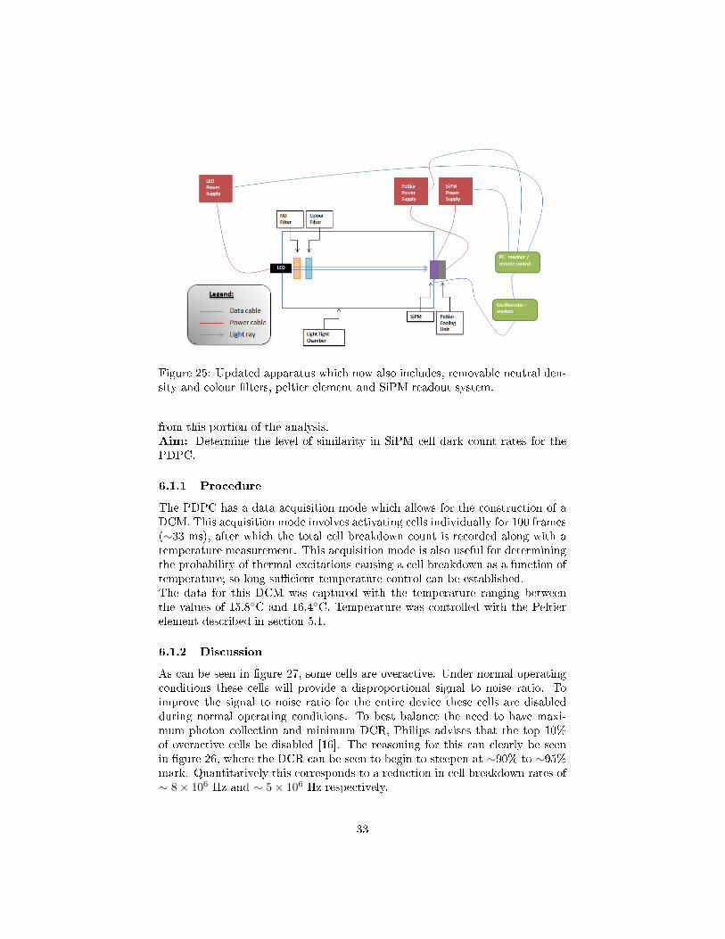
Figure 25: Updated apparatus which now also includes, removable neutral den-sity and colour �lters, peltier element and SiPM readout system.
from this portion of the analysis.Aim: Determine the level of similarity in SiPM cell dark count rates for thePDPC.
6.1.1 Procedure
The PDPC has a data acquisition mode which allows for the construction of aDCM. This acquisition mode involves activating cells individually for 100 frames(∼33 ms), after which the total cell breakdown count is recorded along with atemperature measurement. This acquisition mode is also useful for determiningthe probability of thermal excitations causing a cell breakdown as a function oftemperature; so long su�cient temperature control can be established.The data for this DCM was captured with the temperature ranging betweenthe values of 15.8◦C and 16.4◦C. Temperature was controlled with the Peltierelement described in section 5.1.
6.1.2 Discussion
As can be seen in �gure 27, some cells are overactive. Under normal operatingconditions these cells will provide a disproportional signal to noise ratio. Toimprove the signal to noise ratio for the entire device these cells are disabledduring normal operating conditions. To best balance the need to have maxi-mum photon collection and minimum DCR, Philips advises that the top 10%of overactive cells be disabled [16]. The reasoning for this can clearly be seenin �gure 26, where the DCR can be seen to begin to steepen at ∼90% to ∼95%mark. Quantitatively this corresponds to a reduction in cell breakdown rates of∼ 8× 10⁶ Hz and ∼ 5× 10⁶ Hz respectively.
33
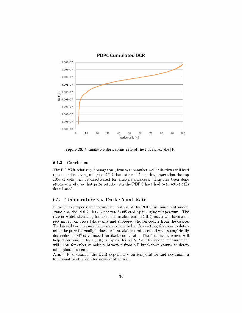
Figure 26: Cumulative dark count rate of the full sensor die [16]
6.1.3 Conclusion
The PDPC it relatively homogenous, however manufactural limitations will leadto some cells having a higher DCR than others. For optimal operation the top10% of cells will be deactivated for analysis purposes. This has been doneretrospectively, so that prior results with the PDPC have had over active cellsdeactivated.
6.2 Temperature vs. Dark Count Rate
In order to properly understand the output of the PDPC we must �rst under-stand how the PDPC dark count rate is a�ected by changing temperature. Therate at which thermally induced cell breakdowns (TCBR) occur will have a di-rect impact on cross talk events and supposed photon counts from the device.To this end two measurements were conducted in this section; �rst was to deter-mine the pure thermally induced cell breakdown rate, second was to empiricallydetermine an e�ective model for dark count rate. The �rst measurement willhelp determine if the TCBR is typical for an SiPM, the second measurementwill allow for e�ective noise subtraction from cell breakdown counts to deter-mine photon counts.Aim: To determine the DCR dependence on temperature and determine afunctional relationship for noise subtraction.
34

Figure 27: Dark count map for full DPC-6400 sensor. Each die has its owncolour map scheme re�ecting the variability between dies. Red cells have thegreatest dark count activity.
35

6.2.1 Procedure
To determine the pure TCBR, data was collected with the DCM data acquisi-tion method with the LED turned o� within the light tight chamber. This wasdone to ensure cross talk was not contributing to the dark count, which onlyleaves thermal excitations as a source of noise. Temperature was controlledby altering the current on the peltier element from 0 A to 2.5 A by .25 A in-crements. Before each data collection a thermal equilibrium period existed toallow the temperature sensor and light sensitive panel time to stabilize. Therelationship between peltier input current and temperature is not well de�ned,with ambient temperature still playing a major role in determining the speci�ctemperature reached.From the collected data the top 10% of overactive cells were removed from fur-ther analysis, the rationale for this is detailed in [16]. The remaining data wasused to generate six versions of the model de�ned by equation 2, each with adi�erent temperature o�set. Included in the model versions was one without atemperature o�set, one with a minimised Chi Square temperature o�set, andvarious o�sets at regular intervals in between these two. The only parameterthat needed to be determined experimentally (apart from the o�set for the �nalmodel version) was the proportionality constant C. This was done with a ChiSquare minimisation algorithm. To determine the e�ective DCR the same pro-cedure was followed as above. However instead of using DCM data acquisition,the frame counting data acquisition cycle was used.Uncertainty Analysis: The internal PDPC temperature sensor has a system-atic uncertainty attributed to the sharp rise in temperature experienced in theshort 100 frame (∼33 ms) capture time per cell. Although a temperature stabi-lization cycle is run, the process of activating cells individually does not allowproper thermal equilibrium. This is represented by the horizontal uncertaintybars used in �gure 28. The statistical and systematic uncertainty in each TCBRbin is of order ∼ 106 which is low enough to not visible with respect to the datapoints themselves. Each model in �gure 28 has an associated residual analysisin �gure 29.
6.2.2 Discussion
The DCM data acquisition cycle turns on individual cells for a period of 100frames (∼33 ms). Given this short time there exists a greater thermal gradientbetween temperature sensor and SiPM cell than would be expected for a framecounting cycle. To account for this a temperature o�set needs to be included inthe model described by equation 2. Various o�sets for our model were includedin �gure 28, however the model which best described the data was for an o�setof 5.33◦C±0.01◦C. This value comes from a reduced Chi Square analysis andis slightly higher than expected by Philips, which only quotes a maximal tem-perature o�set of 4◦C [16]. However there is a clear systematic e�ect for modelversions at o�sets less than 4◦C, as illustrated in �gure 29. This systematice�ect appears to weaken and eventually disappear as the o�set is raised from
36

Figure 28: Temperature vs. Thermal Cell Breakdown Rate including severalmodels with various temperature o�sets to improve curve shape. Each modelhas the form of equation 2, with respective di�erences in C and TOFFSET .
0◦C to 5.33◦C. However this discrepancy between Philips expectations and theresults will be best resolved by further experimentation. Speci�cally, it is rec-ommended a calibrated temperature probe be attached to the PDPC in betterthermal contact with the light sensitive panel. Another option is to use an IRthermometer utilising photons outside of the SiPM cells photo-sensitive range.The temperature o�set used in DCM data acquisition will be di�erent to theframe counter data acquisition. The o�set is in�uenced by the amount of currentrunning through the cell while it is activated to collect data; this amount andthe frequency of current activations are di�erent leading to a di�erent e�ectivetemperature.While a full model construction for noise (thermal + cross talk) would be in-teresting in providing a full description of the device, all which is required is afunctional relationship to describe the noise within a speci�c operating temper-ature. This will be needed for analysis where noise must be subtracted, thusmaking the TCBR model inadequate. The functional relationship is looselybased on the TCBR model, as this was expected to closely mimic the shape.However an extra parameter was included and physical restrictions on the o�-set constant were removed to improve the �t. It should be noted that thisfunctional relationship makes no prediction about o�set temperature, and can-not be expected to be extrapolated upon. Nevertheless temperatures containedwithin the range if this dataset (∼290◦K to ∼306◦K) can be reliably predicted.The residual analysis in �gure 31 does not show any clear sign of a systematic
37

Figure 29: Residual analysis of models in �gure 28.
in�uence.
6.2.3 Conclusion
With the inclusion of a temperature o�set, the PDPC follows the typical SiPMrelationship between TCBR and temperature. This o�set is due to the position-ing of the internal temperature sensor with respect to the light sensitive panelwithin the PDPC device itself. As it is, the two sections which ought to bein thermal contact are separated by a PCB board. Whether the recommendedoperating temperatures were determined with this sensor or an external sensoris of utmost importance. Thus it is highly recommended that further testingwith calibrated sensor in better thermal contact with light sensitive panel.Furthermore the functional relationship established in this chapter will allowfor reliable predictions to be made for the total noise (cross talk and thermal)between ∼290◦K and ∼306◦K.
6.3 Dynamic Range
A basic characteristic of SiPMs is their dynamic range. The bigger the dynamicrange of a device the more useful it will be in general, but knowing the satura-tion point of a device is essential in determining its limitations. Thus �ndingthe dynamic range of an SiPM is essential before its implementation.However, as motivated in section 4 the light source used to determine the dy-namic range of the PDPC has too large incremental steps in its output power.Thus the light will �rst have to be attenuated with the use of neutral density
38

Figure 30: Functional relationship of the dependence of dark count rate ontemperature.
(ND) �lters. This will begin with selection and testing of ND �lters with atrusted device which is not itself under test.Aim: To determine the uncertainty of an independent low level light sensor,then use it to determine the transmittance of ND �lters. Once done, these ND�lters will be used to attenuate the magnitude of the LED output so that anaccurate dynamic range can be determined. Once an appropriate level of lightattenuation is selected, it will be used to determine the dynamic range of thePDPC and Excelitas sample devices in terms of the LED input current.
6.3.1 Apparatus
Two ND �lters (�lter A and �lter B) were used from an unknown manufacturerwith an unquoted transmittance spectrum. These �lters were to be placed inthe chamber between the LED and the PDPC. Filter A was expected to have atransmittance of ∼0.05%, and �lter B a transmittance of ∼5.1%, both with a �atspectrum. Each �lter was tested with the Illumia Lite AQ-80010-005, a handheldspectrometer using charge-coupled devices (CCDs) was used to measure spectral�ux in the range of 380 nm to 820 nm 3.
3Only data between 400 nm and 800 nm was considered as this was the full emission rangeof the LED
39

Figure 31: Residual analysis for functional relationship in �gure 30.
6.3.2 Procedure
To determine the systematic uncertainty on the Illumia Lite AQ-80010-005 thetransmittance curve of a calibrated ND �lter (Thorlabs OD 1.0) was comparedto the known transmittance curve. This calibrated ND �lter was not used forLED attenuation due to its small surface area (radius ∼1 cm).Once the uncertainty of the spectrometer was understood, the device was usedto determine the transmittance per wavelength bin of each �lter (�lter A and�lter B).This was done by measuring the irradiance4 of a light source, thenmeasuring it again with the �lter in place. Dividing the �ltered irradiance bythe other gave the transmittance. Percentage uncertainty was determined byadding the two uncertainties in quadrature.Once the ND �lters transmittance had been veri�ed they were installed in theapparatus between the LED and the PDPC. Then the LED was cycled between0 A to 500 mA in 1 mA increments. The PDPC data recorded in the samefashion as section 5b. However instead of collecting each data point for ∼30minutes, the collection time was reduced to ∼3 seconds. This not only reducedthe collection time of the measurement, but also the time taken to analyse thedata. Three dynamic range measurements were taken; one with �lter A in place,one with �lter B in place, and one with both �lters in place.To capture the Excelitas dynamic range the sample mounted on the DC coupledPCB was used. From there the same procedure as the PDPC was used.
4Irradiance is de�ned as the rate at which energy falls on a surface area. It is measured inunits of W/cm2.
40

Wavelength [nm] 380.0 450.0 555.0 654.5 820.0Spectral Flux Uncert. 6.49% 4.80% 3.96% 3.60% 3.18%
Table 3: Reference Spectral Flux Uncertainty measurements from Illumia [23].
Uncertainty Analysis: The uncertainty in the �gure illustrating the detectedand expected transmittances of the calibrated Thorlabs �lter (�gure 32) comesfrom the manufacturers of the spectrometer itself. The spectrometer came withquoted wavelength dependent systematic uncertainties for its irradiance mea-surements [23]:
Interpolating these values gave a systematic uncertainty for each wavelengthbin. Given that the transmittance (T) is a ratio of the �ltered and un�lteredirradiance (equation 9), the data given in �gures 33 and 34 comes from thiscalculation.
T =IFILTEREDIUNFILTER
(15)
Resultantly, the uncertainty was propagated according to Gaussian Uncer-tainty Propagation:
∆T
T=
√(∆IFILTEREDIFILTERED
)2 + (∆IUNFILTERIUNFILTER
)2 (16)
The value taken for the data points in �gures 35 and 36 is the mean countrate per die. The uncertainty was taken as the standard deviation between therates of the 16 dies.
6.3.3 Discussion
The �gure illustrating the detected and expected transmittances of the cali-brated Thorlabs �lter (�gure 32) clearly shows that these two curves are notin agreement. Should the shape be consistent a calibration of the spectrometerwould be in order. However, there is no more reason to trust this than thereis the systematic uncertainty quoted by Illumia. Thus all we would be doing isexchanging one assumption for another without any particularly good empiricalor theoretical justi�cation.The approach considered more appropriate was to enlarge the systematic uncer-tainty of the measured transmittance to include the expected curve. Arrivingat the new uncertainty of the irradiance from this point is a simple matter offollowing equation 10, with the understanding that ∆IFILTERED
IFILTERED= ∆IUNFILTER
IUNFILTER.
The �gures displaying the �lter transmittances (�gures 33 and 34) both showrelatively �at transmittance spectrums between 400 nm and 800 nm. It is no-table that below 500 nm additional systematic in�uences appear to be a�ectingthe spectrums. The irregular shape here cannot be attributed to the statisticsof small numbers as the data represents an average of ∼20 independent mea-surements. This e�ect is discussed in more detail in section 6.4 where it may be
41
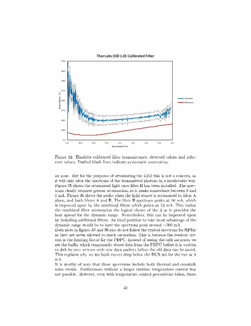
Figure 32: Thorlabs calibrated �lter transmittance, detected values and refer-ence values. Dashed black lines indicate systematic uncertainty.
an issue. But for the purposes of attenuating the LED this is not a concern, asit will only alter the spectrum of the transmitted photons in a predictable way.Figure 35 shows the attenuated light once �lter B has been installed. The spec-trum clearly requires greater attenuation, as it peaks somewhere between 0 and1 mA. Figure 36 shows the peaks when the light source is attenuated by �lter Aalone, and both �lters A and B. The �lter B spectrum peaks at 10 mA, whichis improved upon by the combined �lters which peaks at 73 mA. This makesthe combined �lter attenuation the logical choice of the 3 as it provides thebest spread for the dynamic range. Nevertheless, this can be improved uponby installing additional �lters. An ideal position to take most advantage of thedynamic range would be to have the spectrum peak around ∼500 mA.Both plots in �gures 35 and 36 also do not follow the typical spectrum for SiPMsas they are never allowed to reach saturation. This is because the readout sys-tem is the limiting factor for the PDPC. Instead of seeing the cells saturate, wesee the bu�er which temporarily stores data from the PDPC before it is writtento disk be over written with new data packets before the old data can be saved.This explains why we see both curves drop below the DCR set for the run at 0mA.It is worthy of note that these spectrums include both thermal and crosstalknoise events. Furthermore without a longer runtime temperature control wasnot possible. However, even with temperature control precautions taken, there
42

Figure 33: ND Filter A Transmittance. Dashed black lines indicate systematicuncertainty. Mean transmittance = ∼0.1%.
will still be temperature variations between data points. Given this, for thedynamic range seen we can expect variation depending on ambient temperatureconditions. Finding the relationship between the maximum input current andthe saturation point will only be possible with better information about ambienttemperature.Another drawback of this apparatus for this analysis is the lack of informationabout LED input current and incident photon �ux. To resolve this, a calibratedphoto-detector will have to be installed to analyse the LED output.Figure 37 shows the dynamic range for the Excelitas sample between 0 mA and500 mA for the LED input current. It includes four curves, one for each ND�lter combination. The raw SiPM output voltage was divided by the maximumoutput voltage (i.e. the voltage output for the no �lter case with the LED at500 mA).An unusual feature of this plot is the changing saturation point between thecurves. Although we expect the shape of the curve to change as it does, thesaturation point is expected to remain the same within certain a certain tem-perature dependence �uctuation. Independent analysis on the output voltage�uctuation dependence on temperature saw no more than a ±1 mV variationwithin a normal operating temperature range. The overwhelming dependenceon the saturation point seems to be on the actual ND �lter being used; astransmittance increases the saturation point also seems to increase. There is no
43

Figure 34: ND Filter B Transmittance. Dashed black lines indicate systematicuncertainty. Mean transmittance = ∼7%.
known reason for this to occur and remains an open question of the setup.Despite this inability to precisely determine the saturation point, the resultsdo clearly show a vastly improved dynamic range with respect to the PDPC.For the same level of light attenuation (combined �lter condition) the PDPCdynamic range reaches a maximum at 73 mV, whereas the Excelitas sampledoes not reach saturation. This places a lower limit on the saturation point at500 mV, which represents a × ∼6.6 improvement to the dynamic range beforeaccounting for compression e�ects arising from LED input current to photon�ux conversion.
6.3.4 Conclusion
From �gure 32 we see that the systematic uncertainty on the ND �lters is higherthan referenced. New uncertainty measurements need to be used which accountfor the discrepancy between the detected and referenced transmittance curves.Nevertheless with both ND �lters installed, source light is attenuated enoughto ensure a workable dynamic range is reached. Additionally, the dynamicrange spectrum is not typical of an SiPM. Instead we see the normally expectedspectrum cut o� by the limitations of the PDPC readout system.The Excelitas sample dynamic range on the other hand is quite typical for
44

Figure 35: PDPC Dynamic Range with ND �lter B in place. Dashed linesrepresent systematic uncertainty.
an SiPM (see �gure 37). It displays a sharp rise, followed by a plateau as itapproaches saturation. Attenuating the light only stretches out the sharp riseregion and extends the dynamic range of the device. Although none of theattenuated curves seem to reach saturation, the combination of both �lters stillseems to be a workable option for this apparatus.It is recommended for further analysis that an ambient temperature sensorbe installed so a relationship between the ambient temperature and maximumLED input current can be examined. Also a calibrated photo-detector shouldbe installed to examine the relationship between the LED input current and theincident photon �ux.
6.4 Wavelength vs. Photon Detection E�ciency
Lacking a light source with a tuneable wavelength output it was not possible toverify the PDE varies wavelength directly for the PDPC. However the quotedPDE could be tested with the use of several colour �lters. Ideally this proce-dure would have also been replicated on the Excelitas sample, however withouta calibrated photo-detector in the chamber there was no certain way to convertthe devices voltage output into an irradiance. This paired with a suspectednon linear relationship between voltage output and detected photon �ux in theExcelitas sample would lead to compressions that change the value of any cal-
45

Figure 36: PDPC Dynamic Range with ND �lter A and combined �lters inplace. Dashed lines represent systematic uncertainty.
culated transmittance ratio.Aim: Test the quoted PDPC PDE curve by comparing total irradiance mea-surements with colour �lters in place and removed.
6.4.1 Procedure
Using 3 Kodak gelatine �lters (blue, yellow and red) three independent lightsettings were used. For each case the expected number of photons was calculated(EB , EY and ER) along with the expected number of photons in the absence ofa �lter (EW ). Each value was calculated by �rst determining the emittance ofthe LED (LED), the transmittance of the ND (ND) and colour �lters (CF) andthen combining these with the expected PDPC PDE (PDE) for the resultantwavelength band:
En = LED ×ND × PDE(×CFn) (17)
In this calculation only one colour �lter was used at a time. From this theexpected transmittance of each �lter (TE) was calculated:
TEB =
∫EBdλ∫EW dλ
, TEY =
∫EY dλ∫EW dλ
, TER =
∫ERdλ∫EW dλ
(18)
46

Figure 37: Excelitas Dynamic Range with no ND �lters, �lter A, �lter B andcombined �lters in place. Dashed lines represent systematic uncertainty.
These three ratios were then compared to their corresponding measured trans-mittances (TM ) taken from the PDPC:
TMB =MB
MW, TMY =
MY
MW, TMR =
MR
MW(19)
These measured values (Mn) were found by collecting 11 sets of temperaturecontrolled data for each �lter condition, and looking for coincidences betweenthe �ltered and un�ltered cases. These measured values then had the expectedcrosstalk and thermal noise subtracted from the measurements. Crosstalk isquoted at 25%±1% [16], and thermal noise as a function of temperature wasfound in section 6.2.
When calculating the PDE, three models were used. The �rst was the modelquoted by Philips (PDPC 6400). However this had a shape uncharacteristic ofan SiPM so the second model used was for its sister device (PDPC 3200) whichhad a more typical SiPM response curve, but had an unusual cut o�. The �nalmodel used was a combination of the two, one which retained the fundamentalshape of the PDPC 6400 model, but also included the tail and overall amplitudeof the PDPC 3200 model (PDPC 6400 Adjusted).Uncertainty Analysis: The emittance and transmittance values used in theexpectation calculation were done with the Illumia Lite AQ-80010-005 [23]. Thisdevice is a handheld spectrometer using CCDs to measure the spectral �ux inthe range of 380 nm to 820 nm. The systematic uncertainty on the device (∆CCD) was found by taking the transmittance curve of a calibrated ND �lter(Thorlabs OD 1.0), then comparing it to the known transmittance curve. Thus
47

Figure 38: Normalized LED Emittance. Dashed lines represent systematic un-certainty. The curve was normalized to an integral of 1.
the uncertainty was given by:
∆CCD[%] = 1− Known Transmittance
Detected Transmittance(20)
Where detected transmittance is given by:
Detected Transmittance =Mean IrradianceFILTEREDMean IrradianceUNFILTER
(21)
Because the LED emittance was found by directly measuring of the lightsource, this meant that the uncertainty on this measurement was simply ∆CCD.Two neutral density �lters were used (A and B), with each ones transmittance(TA and TB) being a ratio of two independent irradiance measurements. Theuncertainty on each measurement was found by adding the two uncertainties inquadrature:
∆Tn[%] =√∆CCD[%]2 +∆CCD[%]2 (22)
This same method was used for the uncertainties of the colour �lter transmit-tances (TB , TY and TR).Combining all these uncertainties to get the uncertainty for each En was alsodone by adding in quadrature. Finally each TE ratio had its uncertainty deter-mined by adding the two in quadrature again.
48

6.4.2 Discussion
Figure 39: PDE spectrum quoted in manual the relative systematic uncertaintyon this plot is ±4.3%.
The standout result in this section is the comparison between the measuredand expected transmittances in �gure 42. Comparing the measured value tothe adjusted PDPC shows that the blue �lter is short by between 2.3σ to 3.0σ,over the expected yellow transmittance by between 1.6σ to 2.6σ and within −σand σ of the expected red transmittance depending on which model it is beingcompared. Due to the low statistical uncertainty in �gure 42, the variationfrom the mean must be due to systematic e�ects. However if this variationwere purely systematic we might expect a trend in how the observed data variesfrom the expected data. As it is for lower wavelengths (blue) the transmittanceis less, in the middle (yellow) it is higher, and for longer wavelengths (red) itis equal. However, as stated by Schulze [16], the uncharacteristic oscillationseen in the PDPC PDE model 39, is due to di�ractive e�ects on the SiPMarray grid. Thus a slight variation to the angle of the PDPC to the incidentlight �ux could lead to a di�erent di�raction grating and give a di�erent PDEresponse curve. This could lead to an increased amplitude to the oscillationsproviding a systematic uncertainty which looks distinctly statistical. Althoughsoundly based as a hypothesis this is no conclusion, and is best left as an openquestion for the next phase of setup development where a tuneable light sourcewill be installed. This new setup will also be able to answer the open questionsurrounding the steep cut o� which appears at 730 nm for the 6400 model in
49

Figure 40: Combine ND Filter Transmittance. Dashed lines represent system-atic uncertainty. Mean Transmittance =∼0.007%.
�gure 39, which seems to be caused by a limitation in the device used by Philipsto produce this curve.This small statistical uncertainty (∼10% of the systematic uncertainty) is aresult of the high collection rate of the PDPC and the long collection time. Eventhough only events which were taken in thermal coincidence could be considered,the rates of these coincidences was large, with each set of irradiance data varyingfrom ∼ 2.5 × 10⁵ to ∼ 2.5 × 10⁶. It is clear from the disagreement betweenmeasurement and expectation that there is an undescribed systematic in�uencewithin the experimental design. A possible source is the spectrometer used togenerate the LED, ND and CF curves. However given this had an uncertaintyde�ned by a calibrated ND �lter, it is just as likely that the systematic in�uencecomes from the PDPC curve not being appropriately de�ned.When comparing �gure 38 and the quoted LED emittance curve from Bridgelux[24] a discrepancy appears in the shape of the measured curve and the quotedcurve. What stands out in particular is the shoulder at∼550 nm. This particulardiscrepancy stands as a reminder to experimentalists to always independentlyverify ones own data and not rely on manufactural speci�cations alone.The combined ND �lter transmittance shown in �gure 40 has an interestingshape between ∼400 nm and ∼500 nm. This �uctuation seems to be the resultof an undescribed systematic uncertainty. However, it should be noted thissystematic e�ect seems to be no larger than ∼ 103, which will be outweighedby the systematic uncertainty which has been accounted for. Considering the
50

Figure 41: Kodak �lter transmittance curves with systematic uncertainty rep-resented by the dashed lines.
scale of this plot compared to CF (�gure 41) and the LED (�gure 40), this ise�ectively a �at spectrum (all transmittances are of order 10−4% to 10−5% asopposed to 100% to 101% for the Kodak and ND �lters).
6.4.3 Conclusion
The results of this analysis do not invalidate the PDE curve supplied by Philips(�gure 42). However a question still remain about the nature of the discrepancybetween the quoted 6400 curve and the 3200 curve, which are only magni�edby the fact that the best �t for our data was a curve which was formed asa modi�cation of the two curves combined. It is recommended in the nextiteration of this setup with a tuneable light source the PDPC PDE is directlymeasured to get to the bottom of this.
6.5 Multi Photo-Equivalent Peak Spectrum
As motivated in section 3 a fundamental description of any SiPM includes thecharacteristic peak of the device to a single photon. This was not possible to�nd for the PDPC; as the internal logic of the kit's readout electronics was notaccessible. However it was possible to examine for the Excelitas sample. Thusfor this setup to be capable of future SiPM characterisations it is essential that
51

Figure 42: Expected and measured �lter transmittances, with three expectedmodels represented.
is found.Aim: Find the single PE peak maximum for the Excelitas SiPM.
6.5.1 Apparatus
The setup here is similar to previous setup arrangements; however the PDPCwas replaced with the Excelitas sample mounted on the AC coupled PCB. Nosignal light was used; instead the signal from individual photons was mimickedby thermal breakdowns. Temperature was not controllable given the lack ofback-plate to mount the SiPM on the Peltier element, and lack of thermalsensor to ensure stability. The SiPM was fed through an ampli�er before itssignal reached the oscilloscope.The Oscilloscope used was a LeCroy HDO4000 [25]. It has a bandwidth of 200MHz to 1 GHz, 2.5 GS/s sample rate, a minimum detectable pulse width of 2ns, and a Maximum Input Frequency of 250 MHz.The SiPM ampli�er was a Digikey LMH6629 high speed, low noise device with×10 gain [28].
52

Figure 43: Multi PE peak spectrum with PE peaks given a Gaussian �t andwith means labelled.
6.5.2 Procedure
Data was collected from the Excelitas sample by feeding its signal through adigital oscilloscope. From this data a random sample of signals was collectedwhilst the oscilloscope was set to a random trigger. These signals were collectedas waveforms, each waveform lasted for 100 ns with a digitisation of 400 ps. Intotal 100,000 waveforms were collected for analysis.This raw data was analysed by a pre-existing tool which is fully described inchapter 7.1 of [26]. The result of this analysis was the multi PE peak spec-trum seen in �gure 43. From there a Gaussian curve was �tted to each peak,from which the mean was taken. These four means were combined to give acalculation of the 1 PE pulse height, and give a statistical uncertainty.
6.5.3 Discussion
Figure 43 shows the multi PE peak spectrum for the Excelitas sample on the ACcoupled PCB. The sharp peak at 2 mV comes about from a minimum cut withinthe analysis tool. It would seem unlikely that the 1 PE peak occurs below this
53

Measurement for 1 PElevel from multi PE peaksPeak 1 PE level1 PE 6.18 mV2 PE 5.95 mV3 PE 5.73 mV4 PE 5.85 mV
Mean:5.93 mV
STD:0.19 mV
Table 4: 1 PE level with statistical uncertainty from �gure 43
value as a clear 1 PE peak appears at ∼6.2 mV, with regular peaks appearingat multiples near this value up to 4 PE. Even though there is no light sourcefor the SiPM to detect, thermal excitations will generate the same signal in theSiPM. This will create a 1 PE peak identical to a �ashing light source, andwith crosstalk 2 PE, 3 PE and 4 PE peaks will also become pronounced. Theshoulders of each peak are not symmetric due to after pulses not always beingdetected. The 1 PE peak is easily the most pronounced of the four peaks, witheach resulting peak becoming less de�ned. The main reason for this is becausethe Excelitas sample is made up of an array of 14,400 cells, each with individualdi�erences due to manufactural inconsistencies. Each PE peak is a multiple ofthe 1 PE peak in theory. Thus each one gives an independent measurement ofthe 1 PE peak. This is given in table 4 along with the combined result. Fromthis table the measured 1 PE level is within 1.3 σ, the 2 PE within 0.2 σ, the3 PE within 3.1 σ and 4 PE within 1.7 σ. This is within good agreement andprovides con�dence in the result.Crosstalk probability can also be calculated from this spectrum by dividing thenumber of events above 1 PE by the number of all events. In �gure 1 the 1 PEpeak ends around 10 mV, which gives a crosstalk probability of 23%±1%.
6.5.4 Conclusion
In conclusion the 1 PE peak for the Excelitas sample occurs at 5.93 mV for thegiven setup. This means the setup is capable of determining the 1 PE peak ofSiPMs, albeit with an external ampli�er if need be. This result also shows acrosstalk probability of 23%±1%.Upon the next iteration of the apparatus triggering can be improved by a �asher,and a calibrated light source to map LED input current to incident photon �ux.
54

7 Conclusion
7.1 Silicon Photomultiplier Comparison
Looking at the Excelitas sample and PDPC side-by-side allows for a determi-nation to be made about which would be better suited for use in CHEC.The DCR for each device at 25◦C are essentially equal with the Excelitas sampleDCR at 1.5 × 10⁷ ± 3.0 × 10⁶ Hz/cm2 [27] and the PDPC at 1.7 × 10⁷ ± 3.0× 10⁴ Hz/cm2 [Chapter 6.2]. The crosstalk probability is also comparable withthe PDPC crosstalk probability being 25%±1% [16], and the Excelitas being23%±1% [Chapter 6.5].
Figure 44: PDE of PDPC and Excelitas side-by-side. PDPC PDE from [16],Excelitas from [27]. The uncertainty for the PDPC is represented by dashedlines, and comes about from the uncertainty in the described model explainedin section 6.2.
The one characteristic in which the Excelitas sample clearly outperforms thePDPC is in its dynamic range. In �gures 36 and 37 we clearly see the PDPCdynamic range peaks at an LED input current of 73 mA. This corresponds tocell breakdown rate of 44 MHz/cm2, less than the 100 MHz/cm2 expected back-ground cell breakdown rate from the current HESS data [15].This short coming of the PDPC represents the biggest issue surrounding thePDPC, the readout electronics and �rmware around its SiPMs. Not only doesit limit the dynamic range of the device, but the slow activation time (∼10seconds) will prevent fast triggering making the kit useless to CHEC. ShouldPhilips provide access to the raw SiPMs, they may indeed be competitive with
55

the Excelitas samples. However in the absence of this the logical choice betweenthese two devices is the Excelitas sample.
7.2 Setup Development and Recommendations
As the setup currently stands it is light tight (α=0.01) and temperature con-trolled (within 2.22×10⁻⁴ ◦K
s ±1.11×10⁻⁴ ◦Ks ). This makes it well placed to
determine SiPM dynamic range, dark count rate, photon detection e�ciency,1 PE level and crosstalk probability. Based on the analysis conducted in thisthesis several recommendations stand-out for future setup development.
• Installation of a calibrated photo-detector. This will allow for a mappingof LED input current to emitted photon �ux, which will remove any possi-ble horizontal compression in the Excelitas dynamic range measurements.This will also allow for a PDE measurement similar to that conducted onthe PDPC in section 6.4 to be conducted.
• Installation of a tuneable light source, capable of emitting light in narrowwavelength bins. This will allow for direct measurement of SiPM PDE.
• Installation of a temperature sensor for the SiPM. This will allow a DCRanalysis similar to section 6.2 to be completed.
• Establish precise control over ambient temperature. This will improvetemperature control over the sensor and reduce collection time in mostanalyses.
56

References
[1] Bergstrom, L. & Goobar, A. (2006). Cosmology and Particle Astrophysics,Chichester, UK, Springer, 227 - 236.
[2] Grupen, C. (2005). Astroparticle Physics, Chichester, UK, Springer, 108 -123.
[3] Dumas, D. (2015). SST-2M Technical Design Report. MAN-PO/090614.
[4] Smale, A. (2013, March). The Electromagnetic Spectrum. Retrieved fromhttp://imagine.gsfc.nasa.gov/science/toolbox/emspectrum1.html
[5] Buzhan, P. et al, (2003). Silicon photomultiplier and its possible applications.Nucl. Instr. and Meth(A504), 48-52.
[6] Andreev, V. et al, (2005). A high-granularity scintillator calorimeter readoutwith silicon photomultipliers. Nucl. Instr. and Meth(A540), 368-380.
[7] Coelho, L.C.C. et al, (2007). Xenon GPSC high-pressure operation withlarge-area avalanche photodiode readout. Nucl. Instr. and Meth(A575),444-448.
[8] Ludhova, L. et al, (2005). Planar LAAPDs: temperature dependence, per-formance, and application in low-energy X-ray spectroscopy. Nucl. Instr.and Meth(A540), 169-179.
[9] Moszynski, M. et al, (2003). Avalanche photodiodes in scintillation detection.Nucl. Instr. and Meth(A497), 226-233.
[10] Ni, K. et al, (2005). Performance of a large area avalanche photodiodein a liquid xenon ionization and scintillation chamber. Nucl. Instr. andMeth(A551), 356-363.
[11] Bondarenko, G. et al, (2000). Limited Geiger-mode microcell silicon pho-todiode: new results. Nucl. Instr. and Meth(A442), 187-192.
[12] Aprile, E. et al, (2006). Detection of liquid xenon scintillation light with asilicon photomultiplier. Nucl. Instr. and Meth(A556), 215-218.
[13] Lorenz, E. et al, (2004). Status of the 17 m MAGIC telescope. New Astron.Rev.(48), 339-344.
[14] SensL, (2011). An Introduction to the Silicon Photomultiplier. Rev. 3.1.
[15] Aharonian, F. et al, (2004). Calibration of camera of the HESS detector,arxiv.org/abs/astro-ph/0406658.
[16] Schulze, R. et al, (2013). PDPC-TEK User Manual. Koninklijke PhilipsElectronics.
[17] Datasheet of Hamamatsu SiPM series S10361.
57

[18] Renker, D. et al, (2009). Advances in solid state photon detectors.JINST (4), P04004.
[19] Ramilli, M. et al, (2008). Characterization of SiPM: Temperature depen-dencies. Nuclear Science Symposium Conference Record SS 08. Dresden,Germany, 10.1109/NSSMIC (4774854), 24672470.
[20] Arnold, T. & Emerson, J. (2011) Nonparametric Goodness-of-Fit Tests forDiscrete Null Distributions, The R Journal,(3-2) 34 - 39.
[21] Barlow, R. (1999) Statistics: A Guide to the Use of Statistical Methods inthe Physical Sciences, University of Manchester: Wiley,155 - 165.
[22] Taylor, R.A. et al, (2004). Comprehensive system-level optimization of ther-moelectric devices for electronic cooling applications, IEEE,(Vol:31, Issue:1).
[23] McKee, G. et al, (2012). Illumia Lite Technical Manual, Labsphere Inc..
[24] Bridgelux, Inc. et al, (2011). Bridgelux ES Star Array Series Product DataSheet, Labsphere Inc..
[25] Graef, D. et al, (2013). Operator's Manual HDO4000 High De�nition Os-cilloscope, Teledyne Lecroy. www.teledynelecroy.com.
[26] Stephan, M. (2014). Measurement of the Light Flux of Starsand the Night-Sky with Silicon Photomultipliers, Aachen University.web.physik.rwth-aachen.de/∼hebbeker/theses/stephan_phd.pdf.
[27] Excelitas Technologies. (2013). C30742-66 Series Silicon PhotomultiplierDatasheet with 6x6 mm2 active area. excelitas.com.
[28] Texas Instruments. (2015). LMH6629 Ultra-Low Noise, High-Speed Oper-ational Ampli�er with Shutdown Datasheet. digikey.nl.
58

8 Acknowledgements
This research was supported by CTA, API and NIKHEF. I thank my colleaguesfrom these institutions who provided insight and expertise that greatly assistedthe research. In particular I would like to thank my supervisor David Berge anddaily supervisors Arnim Balzar and Maurice Stephan for assistance and supportduring my research. Also for their comments which greatly improved the �naldraft of this thesis.I would also like to show my gratitude to Niels van Bakel and the NIKHEF R&Dgroup for sharing their research and experience with me over the course of thisproject. I am also immensely grateful to Oskar van Petten, Guido Visser andTaco Walstra for providing hardware support, helping me make my apparatusa reality.
59